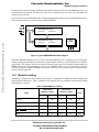
1
Freescale Semiconductor, Inc. AN1722/D Rev. 1.1, 6/2003 Freescale Semiconductor, Inc... SDRAM System Design Using the MPC106 by Gary Milliorn RISC Applications This document discusses the implementation of an SDRAM-based memory system using the MPC106. The MPC106 PCI Bridge/Memory Controller provides a bridge between the Peripheral Component Interconnect (PCI) bus and Freescale's MPC603e, MPC740, MPC750, MPC745, MPC755, MPC7400 and MPC7410 PowerPC™ host processors. To locate any published errata or updates for this document, refer to the website at http://www.freescale.com/SPS/PowerPC/. 1.1 Overview There are numerous possibilities available in designing systems, although most will probably fall into the typical category shown in Figure 1. This document refers to components in Figure 1 when describing the issues involved in creating a PowerPC-based system. Note that many other configurations are also possible. conductor, Inc., 2004. All rights reserved. For More Information On This Product, Go to: www.freescale.com Freescale Semiconductor, Inc. System Analysis MPC106 Grackle TS AACK Freescale Semiconductor, Inc... BCTL[1–0] SDCAS CKE, WE MA[0–12] DQM[7–0] CS[7–0] SDRAS PowerPC Processor Data Bus Buffers Clock SDRAM Memory Discrete or JEDEC DIMM Module Figure 1. Typical SDRAM System Block Diagram Note: High-speed design systems operate at 100 MHz or less. To achieve such a high speed, it necessary to consider each source of possible problems and aggressively pursue solutions. An accurate simulation of the board, taking into account the trace lengths and trace separations, is essential. For designers who are considering lower-speed memory systems, it is possible to ignore some of these considerations. 1.2 System Analysis Important factors to consider when designing an SDRAM-based system follows: • • • • MPC106 AC timing MPC106 output impedance settings SDRAM setup/hold time Time-of-Flight (TOF) The MPC106 timing parameters are generally a function of the operating speed and are fixed; however, other attributes such as output impedance are configurable, and timing relationships between the MPC106 and memories can be achieved by careful adjustments to the clock. The SDRAM components are also generally constant in setup/hold times across many vendors. The contribution of capacitive loading from a typical DIMM socket is negligible, so this document refers to SDRAM modules when referring to the memory. Note that embedded applications using discrete SDRAM memories are equally viable. The last factor is the Time-of-Flight (TOF), which refers to the amount of time it takes for a signal to propagate from one point to another. Unlike the other factors, TOF contains several subordinate factors that have to be considered, and is also affected by the electrical characteristics of the MPC106 and the SDRAM. Figure 2 shows an idealized signal connection between the MPC106 and an SDRAM component. The term “ZO”, for example, is commonly used for both board impedance and output impedance, but it is used in this document exclusively for trace impedance. SDRAM System Design Using the MPC106 For More Information On This Product, Go to: www.freescale.com Freescale Semiconductor, Inc. MPC106 Memory Controller MPC106 SDRAM RS ZO CO LO l ZD RT CL Freescale Semiconductor, Inc... TOF ZD MPC106 Output Impedance CO Trace Capacitance RS Series Termination LO Trace Inductance RT Parallel Termination (Thevenin) CL SDRAM Input Capacitance ZO Trace Impedance I Trace Length TOF Time-of-Flight Figure 2. SDRAM Interconnect Factors With the exception of the bidirectional data bus, which will be discussed later, the SDRAM devices are controlled exclusively with MPC106 outputs driving SDRAM inputs. Thus, the majority of the design can be completed using the model shown in Figure 2. 1.3 MPC106 Memory Controller The MPC106 implements the entirety of the SDRAM controller with the exception of connecting the SDRAM data bus to the processor data bus (discussed in subsequent sections). It is important to have the latest revision of the MPC106 hardware specifications and the latest errata. Only revision 4.0 of the MPC106 supports the timings needed for high-speed designs, as well as the programmable driver options. For more information refer to Appendix A, “Bibliography.” 1.3.1 Output Impedance To support a wide variety of options, the MPC106 has an internal register (PICR1) which can be used to set the output impedance of various parts of the interface (memory control, data bus, PCI). This document only takes into account the memory control bits, although the other capabilities should be kept in mind when designing the rest of the system. Table 1 shows the three valid impedance settings for the memory control I/O drivers. SDRAM System Design Using the MPC106 For More Information On This Product, Go to: www.freescale.com Freescale Semiconductor, Inc. MPC106 Memory Controller Table 1. MPC106 Memory Control Output Impedance Freescale Semiconductor, Inc... MPC106 Output Drive Alias Software Control 20 Ω Medium, Normal OD CR bit#4 = 0 ODCR bit#0 = 1 13 Ω Herculean ODCR bit#4 = 1 ODCR bit#0 = 0 8Ω Zeus ODCR bit#4 = 1 ODCR bit#0 = 1 To minimize power dissipation, ringing, EMI, etc., use the highest impedance. Since none of these impedances match the general range of PCB impedances available (40–80 ohms), either termination will be required or the traces will have to be extremely short. Since this register is controlled via software, it must be initialized soon after reset occurs and before the memory system is initialized or used. This is a fairly standard practice with MPC106-based systems, since the PCI drive level often needs to be specified as well. 1.3.2 DC Timing Parameters The DC parameters are shown in; refer to the latest hardware specifications for updates to this information. These numbers will be used primarily to determine whether or not series or parallel termination resistors would cause excessive current demand in the I/O driver. Table 2. MPC106 DC Electrical Characteristics Symbol Characteristic MPC106 Output Drive Min Typical Max Units Voh Output high voltage (Ioh = -18 mA) all 2.4 3.3 — V Vol Output low voltage (Iol = 14 mA) all — 0.0 0.5 V Ioh Output high current (Voh = 2.4 V) 20 Ω -18 -36 mA 13 Ω -24 -48 mA 8Ω -28 -56 mA 20 Ω 14 28 mA 13 Ω 19 38 mA 8Ω 22 44 mA Iol Output low current (Vol = 0.5 V) Notes: 1. The Ioh and Iol values are dependent upon the strength of the driver selected. 2. Shaded items are derived and are not tested or guaranteed. SDRAM System Design Using the MPC106 For More Information On This Product, Go to: www.freescale.com Freescale Semiconductor, Inc. MPC106 Memory Controller 1.3.3 AC Timing Parameters The AC timing information, shown in Figure 3 and Table 3, may also be obtained from the MPC106 hardware specifications. CLK tctq toh MPC106 OUTPUT Freescale Semiconductor, Inc... 90% 10% tr tf Figure 3. MPC106 Timing Parameters Table 3. MPC106 Memory Timing Parameters Timing, Maximum Signal Description Units 66 MHz 75 MHz 83 MHz 90 MHz 100 MHz tctq Clock to output (SDRAM) 8.0 7.5 7.0 6.5 6.0 ns tih Input hold 0.0 0.0 0.0 0.0 0.0 ns toh Output hold 1.0 1.0 1.0 1.0 1.0 ns tr Rise time 1.0 1.0 1.0 1.0 1.0 ns tf Fall time 1.0 1.0 1.0 1.0 1.0 ns These values are specified at a load of 50pF. If the load is different than this reference point, then the output timing values will have to be derated using the following formula: t actual = t table – ( t factor ⋅ ( 50 – C load ) ) The actual timing may be derived from the value in the timing tables of the MPC106 hardware specifications (as shown in Table 3) along with the capacitive load of the design and the timing derating factor (shown in Table 4). Table 4. MPC106 Timing Derating Factors Drive Strength Output Valid Factor Output Hold Factor Units Normal/Medium 0.056 0.012 ns/pF Herculean 0.043 0.011 ns/pF Zeus 0.030 0.010 ns/pF SDRAM System Design Using the MPC106 For More Information On This Product, Go to: www.freescale.com Freescale Semiconductor, Inc. SDRAM Component Selection With this information, the normal-mode output valid time at 83 MHz for a signal with a 150pF load could be calculated at 12.6ns. The chart in Figure 4 shows the relationships: 16.0 Output Freescale Semiconductor, Inc... Valid (ns) 14.0 12.0 10.0 Zeus 8.0 Herculean Normal 6.0 4.0 2.0 0.0 0 50 100 150 200 Capacitive Load (pF) Figure 4. MPC106 83 MHz Output Valid Derating 1.3.4 Errata Compensation The MPC106 does not meet the hold times required for PCI; refer to the errata for more information. While this is not ordinarily relevant to an SDRAM design, the solution to the PCI hold time problem requires adding delay to the MPC106 clock. Adding this delay to the MPC106 alone would rob the SDRAM section of margin, so the delay has to be added to all system bus components (that is, CPU, cache, SDRAM, and memory buffers). As shown throughout this document, adding deliberate delay time to signals is common to timing problems. It is important to mention here that this timing correction described in the errata is applied independently of any timing adjustments performed. Section 1.12, “Example System,” details this “global” change as well as the individual changes to be made. 1.4 SDRAM Component Selection In order to properly connect to the SDRAM, allowances must be made for the capacitive loading of the signals for each SDRAM device or module present. Each manufacturer of SDRAM memory devices has slight variations of I/O drivers, which causes a somewhat wide range of capacitances the design will have to compensate for. Most desktop designs use the standardization and flexibility afforded by the JEDEC 168-pin DIMM SDRAM memory module, or the small-outline DIMM modules which is very similar. Embedded designs typically do not need the flexibility and cost associated with sockets and so tend to connect SDRAM memory devices on the PCB. SDRAM System Design Using the MPC106 For More Information On This Product, Go to: www.freescale.com Freescale Semiconductor, Inc. SDRAM Component Selection For the purposes of this document, both have been considered since the effects of the DIMM socket are very minimal and can be ignored. Therefore, the issues to be examined relate only to the type and number of memory devices present. Figure 5 shows a typical SDRAM module; a similar arrangement would be used for embedded applications, except perhaps for the serial presence detect (SPD) EEPROM. Freescale Semiconductor, Inc... SDCAS CKE, WE MA[0–12] DQM[7–0] CS[7–0] SDRAS SDRAM Memory Bank 2 64/72 bits 4-18 Devices SPD I2C ROM SDRAM Memory Bank 1 64/72 bits 4-18 Devices D[0–63] SPD[0–2] Figure 5. Typical SDRAM Module Block Diagram Generally, SDRAM modules are 64- or 72-bits wide and comprised of 4 to 18 separate devices. For greater memory expansion, the module can include two separate banks of memory, which doubles the size (and the signal loads). The designer will have to examine the total loads present to determine the total number of DIMMs that can be accommodated. If every type of DIMM module were to be supported, it might be necessary to limit the number of DIMM sockets used; conversely, if only certain types were allowed, more sockets could be supported. 1.4.1 Module Loading Appendix B, “Organization and Loading Factors shows a compilation of SDRAM module loading (unit loads and total capacitance). Table 5 summarizes the appendix into the minimum and maximum loading which might be expected. Table 5. SDRAM Module Loading Typical-Case Modules Loading Worst-Case Modules Loading Min Max Min Max MA[0–n] 21 98 21 98 pF CKE0 21 69 21 69 pF CKE1 — 69 — 69 pF RAS, CAS, WE 21 98 21 98 pF CLK0 21 41 21 41 pF Signal SDRAM System Design Using the MPC106 For More Information On This Product, Go to: www.freescale.com Units Freescale Semiconductor, Inc. SDRAM Component Selection Table 5. SDRAM Module Loading (continued) Typical-Case Modules Loading Worst-Case Modules Loading Min Max Min Max CLK1 — 41 — 41 pF CLK2, CLK3 — 40 — 40 pF DQMB[0–7] 8 25 8 25 pF CS0, CS2 13 46 13 46 pF CS1 — 41 — 41 pF CS3 — 34 — 34 pF DQ[0–n] 9 20 9 20 pF Freescale Semiconductor, Inc... Signal Units As seen in Table 5, the number of capacitive loads can be very high, almost 100 pF in certain cases. Appendix B shows that the high loads are typically caused by the use of 4-bit SDRAM memories; at a minimum of 16/18 per bank, the capacitance of the address and control signals (which must be wired to each SDRAM in parallel) adds up quickly. The embedded board designer can correct for this problem simply by using wider devices. Sixteen-bit–wide memories are generally preferred as the capacitance drops fourfold. Desktop board designers, however, are faced with the dilemma of choosing between designing for the worst possible case (possibly increasing the cost) or restricting operation to a particular set of SDRAM modules (limiting flexibility). Software can enforce restrictions on the quantity and type of SDRAM modules installed by examining the SPD EEPROM for details. Too many loads and the system could (deliberately) refuse to run; alternately, sufficiently clever software could “degrade” the software-programmable timing registers of the MPC106 to allow for slower operation. The remainder of this document concentrates on the worst-case values to show the magnitude of the effort involved, since reducing the loads will only improve the margins and reliability. 1.4.2 Module Timing Table 6 shows an extraction of the AC timing parameters from several manufacturer’s data sheets. To date, all of the SDRAM modules and discrete components will work provided these timing values are allowed for. Some manufacturers do much better on these, such as requiring less setup time. Although, it will be easier to design for those parts, the board will be restricted to only those parts. This is easier to allow for in an embedded design as opposed to a desktop motherboard design where the manufacturer of the module may not be known. SDRAM System Design Using the MPC106 For More Information On This Product, Go to: www.freescale.com Freescale Semiconductor, Inc. Board Technology Table 6. SDRAM Timing Parameters Maximum Time (ns) Freescale Semiconductor, Inc... Name Description 66 MHz 83 MHz 100 MHz 125 MHz tiss Input setup time, SDRAM 3.0 3.0 3.0 3.0 tihs Input hold time, SDRAM 1.0 1.0 1.0 1.0 tohs Output hold, SDRAM 1.0 1.0 1.0 1.0 trs Rise time, SDRAM 1.0 1.0 1.0 1.0 tfs Fall time, SDRAM 1.0 1.0 1.0 1.0 1.5 Board Technology The printed circuit board holding the components also contributes to the delay between the MPC106 and the SDRAM. There are numerous factors which all vary widely, so each will have to be considered abstractly. Some of the factors to consider are: • Trace width • Trace height over ground planes • Trace thickness (copper thickness) • Material used for board • Stackup organization Figure 6 shows a typical 6-layer stack-up for a PCB, perhaps one of the most common types of high-speed boards. (Note: Four layer boards are electrically close but typically have severe routing limitations that make high speed board layout difficult to impossible.) TW TT LAYER 1 - SIGNAL TH LAYER 2 - GROUND TH LAYER 3 - SIGNAL PREPREG Z= TW = TH = TT = LAYER 4 - SIGNAL LAYER 5 - POWER LAYER 6 - SIGNAL Figure 6. Typical PCB Stackup Diagram SDRAM System Design Using the MPC106 For More Information On This Product, Go to: www.freescale.com 50Ω 0.008” 0.005” 0.0137” (1 oz. copper) Freescale Semiconductor, Inc. Board Technology Equations required to calculate propagation delay are shown in subsequent sections. Table 9 provides the typical propagation delay vs. trace width for the board stack shown in Figure 6 and similar types. Recalculation may be necessary for different board stacks. The following characteristics of the traces will also be discussed: • • • • Electrical permittivity Characteristic impedance Capacitance (per inch) Propagation delay (per inch) Freescale Semiconductor, Inc... 1.5.1 Microstripline Calculations The typical PCB stackup shown in Figure 6 produces traces that are routed over a single power or ground trace, producing a microstripline (as opposed to striplines which are surrounded by planes above and below). The following formulas can be used to determine the propagation delay through the board. First, calculate the electric permittivity of the stripline on the circuit board. Permittivity is a measure of the ability to propagate an electric charge through a particular medium, in this case a rectangular slab of copper overlying a large ground plane or power plane. For thin traces, where the width (TW) is greater than or equal to the height above the ground plane (TH), the permittivity of the trace is defined by the following equation: ε THIN εr + 1 εr – 1 = --------------- + -------------- ⋅ 2 2 12 ⋅ TH – 0.5 TW 2 1 + -----------------+ 0.04 ⋅ 1 – --------TW TH Note that if the trace width is equal to the height above the ground plane, the final term disappears. Additionally, at these small dimensions the permittivity of the surrounding air must also be considered, so the effective permittivity of the trace becomes: TT ( ε r – 1 ) ⋅ -------TH ε EFF = ε THIN – --------------------------------TW 4.6 ⋅ --------TH Once the permittivity of the trace is known, the propagation delay can be computed: ∆ TRACE = 84.72 × 10 – 12 ⋅ ε EFF The effective trace width is needed to calculate the other measurements: 1.25 ⋅ TT 2 ⋅ TH TW EFF = TW + ---------------------- ⋅ 1 + ln --------------- TT π This in turn allows calculation of the characteristic impedance of the trace. The formula for this is: 120 ⋅ π Z WIDE = -------------------------------------------------------------------------------------------------------------------------------------------TW EFF TW EFF ------------------ + 1.393 + 0.667 ⋅ ln ----------------- + 1.444 ⋅ ε EFF TH TH The impedance is important to know later, when signal termination is discussed. When PCBs are purchased, the impedance shown above will be the ideal goal for the manufacturers to attain. SDRAM System Design Using the MPC106 For More Information On This Product, Go to: www.freescale.com Freescale Semiconductor, Inc. Board Technology Finally, compute the capacitance of the trace, which is simply: ∆ TRACE C TRACE = ------------------Z WIDE 1.5.2 Example PCB Measurements Using the formulas provided, plug-in the correct parameters for the PCB. Table 7 shows the typical parameters for a high-speed board. Table 7. Selected PCB Electrical Parameters Freescale Semiconductor, Inc... Parameter Description Value Units Notes TH Trace Height (above ground plane) 0.005 in 5 mil TW Trace Width 0.005 in 5 mil TT Trace Thickness 0.00137 in 1 oz. Copper εr Relative Electric Permeability 4.5 — FR4 Material Reduce the equations to get the propagation delay: ε THIN 12 ⋅ 0.005 = 2.75 + 1.75 ⋅ 1 + -----------------------0.005 ε THIN = 3.24 ε THIN 4.5 + 1 4.5 – 1 = ---------------- + ---------------- ⋅ 2 2 ε EFF 0.00137 〈 4.5 – 1〉 ⋅ ------------------0.005 = 3.24 – ---------------------------------------------0.005 4.6 ⋅ ------------0.005 ε EFF = 3.03 – 0.5 12 ⋅ 0.005 1 + -----------------------0.005 – 0.5 + 0.04 ⋅ [ 1 – 1 ] 2 Continuing: Once the permittivity of the trace is known, the propagation delay can be computed: ∆ TRACE = 84.72 × 10 – 12 ⋅ 3.03 ∆ TRACE = 147.47ps/in Thus, for each inch of trace on the board, allow for 147 ps of delay, best case. Remember that only the blank PCB material is being considered. Once loaded, the propagation delay will only increase. Continuing on with the effective trace width: 1.25 ⋅ 0.00137 2 ⋅ 0.005 TW EFF = 0.005 + ---------------------------------- ⋅ 1 + ln --------------------- 0.00137 π TW EFF = 0.007 SDRAM System Design Using the MPC106 For More Information On This Product, Go to: www.freescale.com Freescale Semiconductor, Inc. Time-of-Flight and characteristic impedance: 120 ⋅ π Z WIDE = ---------------------------------------------------------------------------------------------------------------------------0.007 0.007 ------------- + 1.393 + 0.667 ⋅ ln ------------- + 1.444 ⋅ 3.03 0.005 0.005 Z WIDE = 63.83Ω The impedance is important to know later, when signal termination is discussed. When PCBs are purchased, the impedance above will be the ideal goal for the manufacturers to attain. Finally, compute the capacitance of the trace, which is simply: 147.47 C TRACE = ---------------63.83 Freescale Semiconductor, Inc... C TRACE = 2.31pF/in These calculations are used to calculate the timing losses. Remember that all of these are ideal values from which others may be derived. In particular, there are no loads attached and SDRAM loads can be quite severe. 1.5.3 Reference Values Table 8 allows ideal propagation delay and other important calculations to be read from the trace width and height, assuming FR4 material and 1 oz. copper traces. Table 8. Ideal PCB Electrical Parameters Trace Trace Height Width Impedance Inductance Capacitance Propagation Delay 0.005 0.005 63.83 Ω 9.97 nH/in 2.27 pF/in 147.40 ps/in 0.006 0.010 50.40 Ω 11.39 nH/in 1.95 pF/in 152.17 ps/in 0.006 0.008 56.50 Ω 8.50 nH/in 2.67 pF/in 150.43 ps/in 0.010 0.010 65.90 Ω 9.87 nH/in 3.02 pF/in 152.17 ps/in The typical boards are all reasonably close in propagation delay, impedance and capacitance values. If the board routing choices are not known in advance, use any of the above and the final calculations will not change by much. 1.6 Time-of-Flight This section will determine the Time-of-Flight (TOF), which is a measure of the amount of time it takes for an electrical signal to propagate through a PCB trace. The effects of capacitive loading will be discussed. To determine TOF, the following information is required: • PCB characteristic inductance/in • PCB characteristic capacitance/in • SDRAM module capacitive loading SDRAM System Design Using the MPC106 For More Information On This Product, Go to: www.freescale.com Freescale Semiconductor, Inc. Time-of-Flight • Number of SDRAM modules (in parallel) • Longest-routed trace The first three parameters have been covered in the preceding sections. The SDRAM loading must be the worst-case loading on any particular control signal; it does not matter what the lesser-loaded signals do, since the MPC106 presents each with identical timing, if the worst-case Time-Of-Flight works, the best-case will also. Freescale Semiconductor, Inc... The trace length presents somewhat of a problem, as the PCB may not have been routed yet, so trace lengths of 4 and 6 inches is assumed and the results are presented for each. Later, if there is a problem, reduce the trace length or loads and recalculate these equations. To calculate the TOF, a good model of the capacitance of the trace is needed. To this factor, incorporate the capacitance of the pins of the SDRAM modules Cl. Additionally, the modules are not lumped together at one location, but are connected in series. If the modules are assumed to be evenly spaced, as is typical with a memory design, we have the following model of our SDRAM signals, shown in Figure 7. Co CL CL CL No Figure 7. Distributed Capacitance Using this model, use the following equation to calculate the total capacitance seen per unit time: NO ⋅ CL C O ′ = C O + -----------------length This equation says that the total capacitance is that of the trace (Co) plus that of a quantity (No) of pin capacitive loads (CL) distributed along the PCB trace length. In turn, the delay of the trace can be computed by the usual electromagnetic wave equation, but scaled into picoseconds/inch units: ∆′ = 1 × 10 12 ⋅ L O ⋅ C O ′ ( ps/in ) Table 9 shows representative Co' values for three different loading factors—Heavy, Moderate, and Light—best summarized as the total amount of capacitive loading presented. For each of the two trace SDRAM System Design Using the MPC106 For More Information On This Product, Go to: www.freescale.com Freescale Semiconductor, Inc. Time-of-Flight lengths considered, the capacitance varies fourfold. Table 9. Effective Capacitance for Various Design Factors Co' per Trace Length Number of DIMMs CL Per DIMM CL Total Heavy 2 98 pF Moderate 3 Light 1 Units 4" 6" 196 pF 51.27 34.93 pF 45 pF 135 pF 36.02 24.77 pF 60 pF 60 pF 17.27 12.27 pF Using these values and the board inductance calculation (Lo) it is possible to calculate the propagation delay. Then obtain the TOF by scaling by the trace length. Figure 8 shows the propagation delay for the previous set of loading categories and trace length. 4 3.5 3 Propagation Delay (ns) Freescale Semiconductor, Inc... Loading Category 2.5 Heavy 2 Moderate Light 1.5 1 0.5 0 0" 1" 2" 3" 4" 5" 6" Trace Length (in) Figure 8. Time-of-Flight 1.6.1 Point-to-Point Timing If the system consists of only one SDRAM module or memory, then the TOF is complete as-is; however, if there are multiple SDRAM modules connected serially, then the TOF will differ for each device, with devices closest to the MPC106 getting data earlier and those at the end last. SDRAM System Design Using the MPC106 For More Information On This Product, Go to: www.freescale.com Freescale Semiconductor, Inc. Termination Table 10. Propagation Delay and TOF Freescale Semiconductor, Inc... Device Distance Delay TOF’ Units MPC106 0 0 0 ns SDRAM #1 3" 3" * ∆' 2.5 ns SDRAM #2 4" 4" * ∆' 2.8 ns SDRAM #3 5" 5" * ∆' 3.1 ns ... ... ... ... For most systems it will be sufficient to insure that the final device in the chain receives data with the specified timing budget. 1.7 Termination It is virtually impossible to design a high-speed digital system without paying attention to signal termination, and an MPC106-based SDRAM system is certainly no different. At the speeds discussed in this document, pay careful attention to terminating all of the control signals; otherwise, the signals may be corrupted at the destination (the SDRAM), leading to erratic operation or causing a loss of performance (because compensating delay cycles must be added to the controller initialization). It is strongly encouraged that boards be simulated with real data as much as possible. Data should include the following: • • • • IBIS/Spice models for the MPC106 and SDRAM memories Spice models (including trace lengths) for the JEDEC memory modules Estimated or actual trace lengths Estimated or actual crosstalk due to adjacent traces 1.7.1 No Termination It is possible to ignore termination only if the traces are very short; this relationship is described and derived in the book “High-Speed Digital Design: A Handbook of Black Magic” (refer to Appendix A, “Bibliography,” for more information). The maximum trace length is constrained by the relationship: tr Line Delay ≤ --6 so that for the MPC106, where tr, is 1.12 ns, unterminated traces should have no more than 0.166 ns of delay (compare this to the calculation of propagation delay discussed previously), or approximately 1 inch. This is extremely difficult to accomplish without using MCMs, 3D chip-stacks, or other exotic packaging, so most systems will need to use some sort of termination to compensate for the mismatch between the circuit board impedance (40–80 ohms) and the output impedance of the MPC106 (8–20 ohms) Fortunately, this deliberate mismatch can be easily compensated for with termination resistors, and, in addition, will help clean up the signals. The most common means of terminating high-speed digital circuits are parallel, series, and AC termination. SDRAM System Design Using the MPC106 For More Information On This Product, Go to: www.freescale.com Freescale Semiconductor, Inc. Termination 1.7.2 Parallel Termination Parallel termination, also called “Thevenin” or “split” termination, is an ideal means of terminating high-speed signals. Although the total power dissipation is higher than other methods, it is not as severe as may be believed. With the reduction of voltage levels from 5 to 3.3 volts, power dissipation has also fallen in an inverse square proportion. Additionally, the shorter rise time and ability to daisy-chain signals with minimal reflections will be attractive to reach 100 MHz operation. +V Zt Zo R1 Zd Freescale Semiconductor, Inc... R2 Figure 9. Parallel Termination Calculating the parameters for a parallel termination are slightly more involved, because several constraints must be met: • • R1 || R2 should equal Zo Ioh must not be exceeded • Iol must not be exceeded The first calculation is easy; the latter ones are expressed by examining the voltage drop across R1 or R2 when the output driver is at the active low or high state, respectively. Complicating matters is that the output level is not guaranteed to be VCC (+3.3V) or ground, but instead could be at Voh and Vol. The equations to verify then are: VCC – V oh V oh ---------------------------- – --------- > I oh R2 R1 and ( VCC – V ol ) V ol -------------------------------- – -------- > I ol R2 R1 These are simultaneous equations, and so there are potentially numerous solutions, any that meet the requirements would work as well. For example, Table 11 shows some selected resistor pairs and the resulting conditions. Table 11. Parallel Termination Characteristics Case Number R1 R2 Zt Iol Ioh Vmid PDr1 PDr2 1 120 Ω 150 Ω 66 Ω -8 mA +20 mA 1.8 V 65 mW 38 mW 2 86 Ω 250 Ω 64 Ω -0.8 mA +30 mA 2.4 V 91 mW 23 mW 3 150 Ω 120 Ω 66 Ω -14 mA +14 mA 1.4 V 52 mW 48 mW Case 3 provides more balance in the dissipation of power, while case 2 maintains a steady-state level above SDRAM System Design Using the MPC106 For More Information On This Product, Go to: www.freescale.com Freescale Semiconductor, Inc. Termination the active-high threshold. Case 1 is a compromise between the other two. Table 11 also shows the power dissipation required for each case. This power is always dissipated, since there will be a current between any voltage on the net and one (or both) of the resistors. The value received in exchange for this power dissipation is that the rise times of signals on parallel terminated nets is fast; there is little to no reflection to affect the waveform. Additionally, since the waveform has full amplitude all along the net, loads may be placed anywhere along the net with no distortion of the signal, making it ideal for routing memory busses which tend to be very parallel and perfect for the sort of point-to-point (daisy-chain) wiring that allows. 1.7.3 Series Termination Freescale Semiconductor, Inc... Series terminated systems place a series resistor in series with a signal near the driver pin, as shown in Figure 10. Zs Zd Zo Figure 10. Series Termination The design of a series termination is fairly simple—the value chosen for Zs is such that it, plus the output impedance (Zd), equals the board impedance (Zo). As an example, if the MPC106 is configured for 8 Ω outputs, and the PCB is designed with 50 Ω traces, then the series termination resistor should ideally be 42 Ω. Series terminated signals will typically dissipate much less power than a parallel terminated equivalent. For such circuits, power is dissipated only during the interval when the signal propagates from the source to the destination and back (at which time the signal is critically dampened). Once the net quiesces, no additional power is drawn because both the source and the destination are at equivalent voltage levels. Series terminations are therefore ideal for low-power applications such as notebook computers and certain classes of embedded controllers. To calculate the power dissipations, assume that the net has been charged to +3.3V or ground +0V, and that the MPC106 will drive the net to the opposite state (not Vol or Voh, which are minimums). Calculate the currents needed and insure that they do not violate the specification of the MPC106, and that the power dissipation of the resistor is not exceeded. Using the previous example, the respective Iol or Ioh values would be ±78 mA, and the 255 mW. These numbers exceed both the MPC106 specification on current sink/source, and the maximum power dissipation in a typical resistor network or discrete component (usually around 100 mW). These are, however, peak currents, and as noted previously, current flows only during the propagation of the signal on the net. Therefore, the current and the average power dissipation are both scaled by the proportion of the bidirectional reflection of the signal to the clock period: I MAX ⋅ 2 ⋅ TOF I AVG = ------------------------------------T CLK P MAX ⋅ 2 ⋅ TOF P AVG = -------------------------------------T CLK Assume a 75 MHz system bus and a TOF of 2.5 ns, as discussed previously, to get an average current draw of power dissipation of 30 mA and 98 mW, acceptably within the limits. Thus, while the peak current needs are the same as a parallel circuit, the average current needs are smaller. SDRAM System Design Using the MPC106 For More Information On This Product, Go to: www.freescale.com Freescale Semiconductor, Inc. Termination Because series terminated circuits are stable until the reflected wave has completed, wiring signals in a point-to-point manner creates problems. The preferred wiring for series terminated circuits is to connect only one load to the network. If the signal must be shared, connect the loads using equal-length traces from a short common point near the destination. This is discussed in Section 1.11, “Physical Layout.” Series terminated circuits are the easiest to design and they are attractive in terms of power dissipation and cost. Their drawbacks include an increased rise time (two times that of parallel/AC methods), and the inability to route signals point-to-point. 1.7.4 AC Termination Freescale Semiconductor, Inc... If the signal can be assured of DC balance, in which the net assumes that the logic high and logic low state are roughly equally, the AC termination may be used as shown in Figure 11. Zo Zd Zo Ct Figure 11. AC Termination AC termination is generally only suitable in an MPC106-based system for the SDRAM clocks, all other signals exhibit significant amounts of time in either the high or low state. The attractiveness of AC termination arises from the ability of the periodic transitions of the signal to charge the capacitor to an average voltage level of VCC/2. This in turn cuts the power dissipation to: 2 P AVG VCC ------------- 2 = --------------------ZO In the example of 65 Ω board traces, the power dissipation is 41 mW, less than half that of the parallel terminator. AC terminators are fairly simple to design—the impedance of the termination resistor (Zo) equals that of the board impedance. The capacitor (Ct) is chosen such that the RC time constant of the two allows the voltage to decay during the clock interval. For a 10 ns clock, a suitable Ct would be around 150 pF. AC terminations share the benefits of parallel terminators (to which they are closely related), such as point-to-point routing, while eliminating the undesirable power wasted. 1.7.5 Summary Table 12 summarizes the salient features of each type of termination. The actual values for rise time and power dissipation vary depending upon the components chosen. SDRAM System Design Using the MPC106 For More Information On This Product, Go to: www.freescale.com Freescale Semiconductor, Inc. Clocks Table 12. Termination Characteristics Termination Type Signal Rise Time Point-to-Point Wiring Typical Power Dissipation Recommended For Parallel 1.1ZoCo' Yes 120 mW ≥ 83 MHz; Desktop Systems Series 2.2ZoCo' No 98 mW ≤ 83 MHz; Low-power Systems AC 1.1ZoCo' Yes 41 mW Clock Signals Freescale Semiconductor, Inc... The best termination for a specific application depends heavily upon the physical environment, PCB size, and various other factors. 1.8 Clocks A critically important issue in the design of an SDRAM system is the clocking. To get the high speeds, every important part of the SDRAM array is clocked at the maximum transfer rate, which is as high as 100 MHz. Clearly, these speeds require careful attention to loading and routing in order to assure that each part of the memory system is in sync. An important consideration to keep in mind when designing a clocking scheme is that the MPC106 is a fully synchronous design, and synchronizes all CPU bus activity (which includes memory accesses) by multiplying its PCI clock input with a PLL to match the CPU bus. This means that the MPC106’s clock must be skew-controlled with respect to the CPU bus clocks, even though they are not usually the same frequency group. Most of the clock controllers on the market do not follow this specification; in fact, most typically allow the PCI clocks (that is, the MPC106 clock input) to lag the CPU clocks by 1–4 ns. MPC106-based systems must select clock chips which can generate a bus frequency (66/83/100 MHz) synchronized within 250 ps of the PCI frequency (25–33 MHz). Thus, the basic clock architecture builds on the basic diagram shown in Figure 12. SDRAM System Design Using the MPC106 For More Information On This Product, Go to: www.freescale.com Freescale Semiconductor, Inc. Clocks 50–100 MHz 250 ps skew Freescale Semiconductor, Inc... ÷1 PowerPC CPU L3 Cache Memory (SDRAM) CPU Clocks 50–100 MHz ÷2/÷2.5/÷3/... MPC106 PCI Devices PCI Clocks 25–33 MHz Figure 12. Basic Clock Generation Each SDRAM memory component requires a clock, with clock skew controlled to within the tolerances for setup and hold. JEDEC DIMM modules have from 4- to 18-SDRAM memories on them, controlled by 1 to 4 clock pins. The clock system for SDRAMs attached to the system board can be controlled by the clock system by balancing the loads and distributing them equally. DIMM modules, however, introduce an additional complication because it is unknown what sort of module will be installed, so a clock system that controls any possible module must be designed. Further complicating matters is that different module manufacturers have different approaches as to how clock lines are connected on the module. Table 13 shows all known clocking schemes. SDRAM System Design Using the MPC106 For More Information On This Product, Go to: www.freescale.com Freescale Semiconductor, Inc. Clocks Table 13. Common SDRAM Clock Architectures Module CLK1 Size 8 Mbytes (4) 1Mx16 10 Freescale Semiconductor, Inc... 10 16 Mbytes 64 Mbytes 64 Mbytes (8) 2Mx8 (8) 8Mx8 (8) 4Mx16 10 32 Mbytes 128 Mbytes (16) 2Mx8 (16) 8Mx8 10 10 10 16 Mbytes 64 Mbytes (9) 2Mx8 (9) 8Mx8 10 10 32 Mbytes 128 Mbytes (18) 2Mx8 (18) 8Mx8 10 10 32 Mbytes (18) 2Mx8 10 10 32 Mbytes 32 Mbytes CLK2 CLK3 CLK4 10 10 10 10 10 (No) Type (18) 4Mx8 (18) 2Mx8 10 10 1 2 3 4 1 2 3 4 10 1 2 3 4 10 1 2 3 4 5 10 1 2 3 4 5 10 1 2 3 4 10 1 2 3 4 10 10 10 10 10 10 10 1 2 3 4 1 2 3 4 10 10 1 2 3 4 1 2 3 4 10 1 2 3 4 5 10 1 2 3 4 5 10 1 2 3 4 5 10 10 10 10 10 10 1 2 3 4 10 1 2 3 4 10 1 2 3 4 5 10 1 2 3 4 10 10 10 10 1 2 3 4 1 2 3 4 1 2 3 4 5 The ideal clocking system is shown in Figure 13, where there is one clock driver for each SDRAM clock pin in the system, as well as ones for the MPC106, CPU, memory data bus transceivers, L2/L3 cache, etc. SDRAM System Design Using the MPC106 For More Information On This Product, Go to: www.freescale.com Freescale Semiconductor, Inc. Clocks Zs Zo CLK1 CLK2 SDRAM CLK3 CLK4 Low-Skew Clock Driver Zs CLK1 CLK2 SDRAM Freescale Semiconductor, Inc... CLK3 CLK4 ... ... ... Figure 13. Ideal Clock Architecture Not shown in Figure 13 are the clocks for the CPU, cache, MPC106, PCI slots and devices, etc. This architecture usually becomes prohibitively expensive when there are many SDRAM modules/memories because there may not be enough clock signals to control the remainder of the system. An alternate possibility is a distributed clock generation system as shown in Figure 14. Here a single system clock driver signal drives a remote PLL-based clock driver. These secondary clock chips synchronize themselves to the input source, allowing the outputs to maintain 0-ns skew with relation to the master clock. These chips are often referred to as “robo-clocks”, because they do no synthesis, but only replicate the input to multiple outputs. This architecture can benefit boards with routing density problems (typically densest is the CPU/MPC106 area) by requiring only one clock line to be routed over to the SDRAM array. This also frees up many other clock outputs to be used elsewhere. The disadvantage, of course, is the additional cost of the robo-clock. SDRAM System Design Using the MPC106 For More Information On This Product, Go to: www.freescale.com Freescale Semiconductor, Inc. Clocks Zs CLK1 Zo CLK2 SDRAM CLK3 CLK4 No-Skew Robo-Clock Driver Low-Skew Clock Driver CLK1 Freescale Semiconductor, Inc... Delay Compensation Feedback CLK2 SDRAM CLK3 CLK4 ... ... Figure 14. Distributed Clock Architecture If the above examples are not possible, usually due to an insufficient number of clock outputs and/or cost problems, then compromises in the clock generation and attempts to compensate for them must be explored. In each of the remaining cases, the capacitive loading increases and so the propagation delay does also. This means that the timing must be carefully analyzed in light of the new side effects. One possibility is to share clock lines for the SDRAM modules. Table 13 shows several combinations. One good possibility is to combine CLK1 with CLK3, and CLK2 with CLK4. This works well with the 72-bit wide modules, distributing the clock lines with 5 loads so that no clock line must drive more than one such load. It also works well with the smaller modules which have no loading on CLK3 or CLK4 at all. This technique works regardless of whether or not DIMMs are used; if not, just connect the clocks as shown in Figure 15. SDRAM System Design Using the MPC106 For More Information On This Product, Go to: www.freescale.com Freescale Semiconductor, Inc. Clocks CLK1 Zs Zo CLK2 SDRAM CLK3 CLK4 Low-Skew Clock Driver CLK1 Zs Zo CLK2 SDRAM Freescale Semiconductor, Inc... CLK3 CLK4 ... ... ... Figure 15. Shared Clock Architecture Note that this example shows series termination for the clock lines. To handle the reflections for this type of termination we would attempt to equalize the “Y” branch at the destination, keeping each split of the trace as short as possible but also equal to the other branch. While some reflection is inevitable, this will minimize the effects during the settling of the reflected waveform. In a manner similar to this one, we can also share the outputs of the clock driver, as shown in Figure 16. By splitting clock trace near the clock driver, and routing two equal-length traces, we can drive one SDRAM module with one clock pin. This method requires a clock driver with a sufficiently low output impedance, and special changes to the series termination. CLK1 Zs' Zo CLK2 SDRAM CLK3 Low-ZD Low-Skew Clock Driver CLK4 CLK1 Zs' Zo CLK2 SDRAM CLK3 CLK4 ... ... ... Figure 16. Multiply Shared Clock Architecture SDRAM System Design Using the MPC106 For More Information On This Product, Go to: www.freescale.com Freescale Semiconductor, Inc. Clocks The board impedance can be calculated using the formulas discussed in Section 1.5, “Board Technology.” As an example, the Freescale MPC972 clock generator meets the general requirements of a PowerPC clock source, and additionally has a 7Ω output impedance. The relationship is determined by the following equation: Z D Ω + Z S' Ω || Z S' Ω = Z O Ω || Z O Ω So plugging in what we know: 7Ω + Z S' Ω || Z S' Ω = 50Ω || 50Ω Or, simplifying: Freescale Semiconductor, Inc... Z S' Ω = 2 ⋅ ( 25Ω – 7Ω ) = 36Ω 1.8.1 Clock Offset At this point the clocks are wired to the SDRAM, but there is one other factor to consider—the capacitive loading on the clock signals and its’ effect on the clock. Worst-case loading will be around 40pF per clock signal, refer to Section 1.4, “SDRAM Component Selection,” for more information. When we previously calculated TOF values, we used the worst-case loading factors for signals such as SDCAS. Clocks tend to be loaded somewhat less, since there are more of them, so recalculating the TOF factors for the clock (TOFCLK) gives a faster propagation delay. Thus, the clock arrives significantly before the signal, robbing the SDRAM of the hold time that is normally present. These differences in the Time-of-Flight will need correction, so the routing of the clock signals will need adjusting relative to the more-heavily loaded control and data signals, refer to Figure 17. In fact, a deliberate offset to the clock signals (usually via additional trace length) may be needed to achieve high-speed operation. Uncompensated Clocks: TOFCLK = 1.6ns Clock Cl = 45pF MPC106 Cl = 98pF CLK SDRAM SDCAS TOF = 2.3ns Compensated Clocks: TOFCLK = 2.3ns Clock Cl = 45pF MPC106 Cl = 98pF TOF = 2.3ns Figure 17. Clock Trace Compensation SDRAM System Design Using the MPC106 For More Information On This Product, Go to: www.freescale.com CLK SDCAS SDRAM Freescale Semiconductor, Inc. Clocks 1.8.2 Clock Errors One final consideration with regard to the accuracy of the clock signals is that clock drivers are not perfect and have their own sources of errors—cycle-to-cycle jitter and pin-to-pin skew. The jitter specification must be tightly controlled or some cycles may be shortened, causing data loss. Therefore, tight jitter control is needed. Pin-to-pin skew means that some clock pins will change state at a slightly different time from the rest of the pins; this also has the effect of possibly shortening an SDRAM access time. Both of these errors must be allowed for when calculating the timing accuracy of the system. Freescale Semiconductor, Inc... 1.8.3 Clock Drivers Table 14 lists compatible clock drivers for SDRAM-based systems. Note that since the processor, MPC106, memory buffers and SDRAM are all +3.3V, only LVTTL clock generators may be used. SDRAM System Design Using the MPC106 For More Information On This Product, Go to: www.freescale.com Freescale Semiconductor, Inc. Timing Analysis Table 14. Compatible Clock Drivers Freescale Semiconductor, Inc... Component Max System Clock Clock Counts System Clock Skew (Max) PCI System to System System to PCI Max Jitter 3:2 Mode Support Freescale MPC972 200 MHz 8 4 350 ps 500 ps ±100 ps Yes Freescale MPC950 180 MHz 4 6 375 ps 500 ps ±100 ps No Freescale MPC980 66 MHz 6 4 350 ps 350 ps ±150 ps No ICWorks W42B972 200 MHz 8 4 350 ps 500 ps ±100 ps Yes MicroLinear ML6500 80 MHz 4 4 300 ps 300 ps ±150 ps Yes TI CDC586/CDC2586 100 MHz 6 6 500 ps 500 ps ±200 ps No AMCC SC3506 80 MHz 10 10 500 ps 500 ps ±0 No 1.9 Timing Analysis Figure 18 shows how the previously selected timing factors will be used together. CLK TCTQG TOHG MPC106 OUTPUT TOF TSUS SDRAM INPUT TOHS TCTQS SDRAM OUTPUT THI MARGIN* Note: The timing gap ‘Margin’ is the total allowance for errors due to system noise, clock jitter, clock skew and a host of other problems. The greater the margin, the greater the reliability and robustness of the SDRAM memory system. Figure 18. MPC106 Timing Analysis Since TOF is dependent upon the trace length, which may not be well known in advance, a useful first step in checking the timing is to compute the TOF and margin as a remainder of the other timing factors (see Table 15). SDRAM System Design Using the MPC106 For More Information On This Product, Go to: www.freescale.com Freescale Semiconductor, Inc. Timing Analysis Table 15. TOF and Margin Remaining Bus Speed Measurement Units Freescale Semiconductor, Inc... 66 MHz 75 MHz 83 MHz 90 MHz 100 MHz Initial time interval 15.2 13.3 12.0 11.1 10.0 ns MPC106 CLK-to-output-valid -8 -7.5 -7 -6.5 -6 ns Clock skew -0.5 -0.5 -0.5 -0.5 -0.5 ns Clock jitter -0.3 -0.3 -0.3 -0.3 -0.3 ns Termination-induced slew delay -0.0 -0.0 -0.0 -0.0 -0.0 ns SDRAM input-setup -3.0 -3.0 -3.0 -3.0 -3.0 ns TOF + Margin 3.4 2.0 1.2 0.8 0.2 ns An examination of these numbers discloses a large allowance for margin and TOF at 66 and 75 MHz, so a reasonable expectation is that the operation at these two frequencies will be successful. The remaining allowances at 83 MHz and beyond are very small, and we have yet to allow for PCB traces, so clearly there are some obstacles to overcome. Table 16 provides more specific information regarding TOF + Margin. Table 16. Margins Bus Speed Measurement Conditions 75 MHz 83 MHz 90 MHz 100 MHz 3.4 2.0 1.2 0.8 0.2 ns 4" traces, light load -1.6 -1.6 -1.6 -1.6 -1.6 ns 6" traces, light load -2.0 -2.0 -2.0 -2.0 -2.0 ns 4" traces, heavy load -2.7 -2.7 -2.7 -2.7 -2.7 ns 6" traces, heavy load -3.4 -3.4 -3.4 -3.4 -3.4 ns 0.7...1.8 0.4 — — — ns TOF + Margin TOF Units 66 MHz Margin As expected, once the PCB traces are included (through the TOF factor), most of the table entries are no longer viable. Clearly, most designs are not suitable using the basic defaults specified (series termination, worst-case loading, normal clock routing). Ways to overcome these problems are discussed in the rest of this section. 1.9.1 Hold Time Before examining solutions to the setup time problems, insure that the SDRAM input hold times are met. Table 17 compares the MPC106 and SDRAM components’ requirements. SDRAM System Design Using the MPC106 For More Information On This Product, Go to: www.freescale.com Freescale Semiconductor, Inc. Timing Analysis Table 17. System Hold-Time Analysis Timing Budget Freescale Semiconductor, Inc... Measurement Units 50 MHz 66 MHz 75 MHz 83 MHz 100 MHz MPC106 CLK-to-output-invalid (output hold) 1.0 1.0 1.0 1.0 1.0 ns Flight-time 0.5+ 0.5+ 0.5+ 0.5+ 0.5+ ns SDRAM input hold -1.0 -1.0 -1.0 -1.0 -1.0 ns Timing margin 0.5+ 0.5+ 0.5+ 0.5+ 0.5+ ns Ignore the TOF at this point. The requirement here is that the SDRAM inputs must not change for 1.0 ns after the clock edge. If the clocks are in sync, then a long TOF only lengthens the hold time; the SDRAM input will see no change until TOF + 1.0ns. In fact, in Table 17, the TOF time is the timing margin. 1.9.2 Insufficient Margin If, because of heavy loading by the SDRAM parts, or PCB layout restrictions, there are no margins (or perhaps the margins do not meet the basic TOF requirements), some additional work will have to be done. If, on the other hand, the margins are acceptable for the system being designed, go directly to Section 1.8.3, “Clock Drivers.” If more margin is needed, first, try changing the definition of the problem so the problem solves itself. In this case, restrict the type and/or number of SDRAM modules allowed to be installed (embedded systems designers get to do this for free just by changing the bill of materials). While this might seem like cheating, Appendix B, “Organization and Loading Factors,” shows that the most heavily-loaded modules are dual-bank DIMMs and those which use 4-bit-wide memories; restricting the free use of those particular types can reduce capacitive loading by one-half to one-fourth. Take, for example, a Samsung KMM366S824AT (64 Mbyte 1-bank x16) SDRAM module, where the input setup time is reduced to 2.0 and 2.5 ns at 83 MHz and 100 MHz, respectively. A revised margin table is shown in Table 18. SDRAM System Design Using the MPC106 For More Information On This Product, Go to: www.freescale.com Freescale Semiconductor, Inc. Timing Analysis Table 18. Margins with Faster Modules Bus Speed Measurement Conditions 75 MHz 83 MHz 90 MHz 100 MHz 4.4 3.0 2.2 1.3 0.7 ns 4" traces, light load -1.6 -1.6 -1.6 -1.6 -1.6 ns 6" traces, light load -2.0 -2.0 -2.0 -2.0 -2.0 ns 4" traces, heavy load -2.7 -2.7 -2.7 -2.7 -2.7 ns 6" traces, heavy load -3.4 -3.4 -3.4 -3.4 -3.4 ns 1.7...2.8 0.3...1.4 0.2...0.6 — — ns TOF + Margin Freescale Semiconductor, Inc... TOF Units 66 MHz Margin This has opened up a few cases at 75 and 83 MHz, but the higher speeds are tantalizingly out of reach. A glance at Table 15 yields no interesting ideas. Tightening up the clock specifications would obtain, given an absolutely perfect clock, a margin gain of only 800 ps; scarcely enough for a lightly-loaded 90 MHz bus and nothing else. Clearly, the clock-to-output time (TCTQ) of the MPC106 is the stumbling block here. If we could do something about TCTQ we might have something. 1.9.3 Clock Offset The final approach to increasing margin addresses the problem of the clock-to-output time (TCTQ) of the MPC106. Clearly we cannot change the chip to alter these fundamental timing values, so instead we approach from a different direction. Until now, we have assumed that the MPC106, the CPU and the SDRAM were all exactly synchronized (with the usual error allowances). However, by introducing a deliberate clock offset to the SDRAM, all of its timing parameters will be offset with respect to the remainder of the system. Figure 19 shows the standard MPC106/SDRAM timing waveform, except that the SDRAM now receives a slightly delayed clock. SDRAM System Design Using the MPC106 For More Information On This Product, Go to: www.freescale.com Freescale Semiconductor, Inc. Timing Analysis TOF overlaps TSU CLK TCTQG TOHG MPC106 OUTPUT TOF NORMAL SDRAM INPUT TSUS Freescale Semiconductor, Inc... TCTQS TOHS NORMAL SDRAM OUTPUT TCLKO THIS OFFSET CLK TSUS' OFFSET SDRAM INPUT TCTQS' OFFSET SDRAM OUTPUT TOHS' THIS' Figure 19. MPC106 Offset Clock Timing Diagram Figure 19 has zero margin, since TSUS' starts at the end of TOF; the important feature to note is that TSUS' has been delayed to that time at a minimum; additional delay is acceptable to increase margins. Essentially, the purpose of the clock offset is to give the SDRAM extra setup time by taking it from the output hold time. This is possible in that, as noted before, the TOF adds to the apparent hold time, so subtracting some violates no timing requirements. The only concern that arises is the clock-to-output timing of the SDRAM data bus (TCTQS') which, because it is typically lightly loaded and feeds directly into a registered transceiver, can usually be compensated for (but be sure to read the section on the data bus). A revised margin table is shown in Table 19 in which a nominal amount of clock offset has been added (a sufficient amount to give a small positive margin in all cases). SDRAM System Design Using the MPC106 For More Information On This Product, Go to: www.freescale.com Freescale Semiconductor, Inc. Timing Analysis Table 19. Margins (Faster Modules, Clock Offset) Bus Speed Measurement Conditions Freescale Semiconductor, Inc... TOF + Margin Units 66 MHz 75 MHz 83 MHz 90 MHz 100 MHz 4.4 3.0 2.2 1.3 0.7 ns Clock offset Frequency dependent +0.0 +0.7 +1.5 +2.4 +3.0 ns TOF 4" traces, light load -1.6 -1.6 -1.6 -1.6 -1.6 ns 6" traces, light load -2.0 -2.0 -2.0 -2.0 -2.0 ns 4" traces, heavy load -2.7 -2.7 -2.7 -2.7 -2.7 ns 6" traces, heavy load -3.4 -3.4 -3.4 -3.4 -3.4 ns 1.7...2.8 0.3...2.1 0.3...2.1 0.3...2.1 0.3...2.1 ns Margin The margins are the same in all cases over 66 MHz because the clock offset was chosen that would give a minimum of 0.3 ns margin. An alternate way to approach this, not covered here, is to select a particular clock offset and compare the margins remaining. This is particularly attractive if the target system must operate at numerous bus speeds (as with programmable PC motherboards). The delays necessary to implement the clock offsets shown above can be implemented on a PCB by creating delay line traces, and is discussed in the following section. Note that in the 100 MHz case, a 3.0 ns delay is required. While this is certainly possible on a PCB, it constitutes 30% of the 10 ns cycle time at that speed, just for a corrective factor alone. That is a good hint that a heavily loaded bus may not be able to function at very high speeds. 1.9.4 PCB Delay Lines To implement the delay on the PCB, re-use the equations from Section 1.6, “Time-of-Flight.” Be careful to use the capacitance of the clock inputs, which are not necessarily the worst-case loads for a particular SDRAM module. Additionally, the clock inputs are often driven by dedicated signals and so are not necessarily affected by the number of modules (though this depends upon the clock architecture chosen). Table 20 illustrates a range of loading for clock signals from 25 to 55pF. We can use these values to determine amount of PCB trace we will need to implement the necessary clock offset. SDRAM System Design Using the MPC106 For More Information On This Product, Go to: www.freescale.com Freescale Semiconductor, Inc. Timing Analysis Table 20. Clock Offset Trace Length Calculation Conditions Co ' (pF) ∆ (ps/in) Clock offset Freescale Semiconductor, Inc... Delay line length Bus Speed Units 66 MHz 75 MHz 83 MHz 90 MHz 100 MHz +0.0 +0.7 +1.5 +2.4 +3.0 ns 55 pF, 4" trace 16.0 399 — 1.75 3.75 6.00 7.51 in 55 pF, 6" trace 11.4 337 — 2.00 4.45 7.12 8.90 in 25 pF, 4" trace 8.5 291 — 2.40 5.15 8.24 10.30 in 25 pF, 6" trace 6.43 252 — 2.77 5.95 9.52 11.90 in These trace lengths are quite long, but are easily implemented on a PCB if sufficient routing area is available. Figure 20 shows a delay line which can be implemented on a typical FR-4 PCB. Take the 8.9 inch delay line for the moderately loaded 100 MHz system from Table 20, for example. Assuming 50 Ω PCB traces, lay out the delay line as shown in Figure 20. 1. If PCB is 0.010: TW = 2 x TH = 0.020 2. Add extra trace separation to reduce crosstalk: TW + 0.010 3. Center-to-center dimension is then: 2 x TH + 0.010 = 0.050 0.050 0.600 4. Pick a width to fit the available space: 0.600 5. Number of crenelations: Length/(0.600 x 2 + 0.0500 x 2) Figure 20. Delay Line The above example would give the following delay line parameters: Copies of delay segment: 7 Total Area: 0.7" L x 0.6" H = 0.42 in2 When designing the delay line, keep in mind that the accuracy/inaccuracy of PCB fabrication houses and natural temperature variances of FR-4 PCB materials can cause the accuracy of the delay line, shown in Figure 20, to vary by 10%. 1.9.5 Determining How Much Margin So far, we have designed with a minimum target of 300 ps. This figure was arbitrarily chosen to provide a 10% margin at 100 MHz; there is no reason less or more margin could not be used, provided all other SDRAM System Design Using the MPC106 For More Information On This Product, Go to: www.freescale.com Freescale Semiconductor, Inc. The Data Path constraints are not violated. The choice for a margin amount must be an educated guess on the part of the system designer. If the target system is expected to have any of the following problem sources then a larger margin is needed: • • • • • • Electrically noisy High levels of crosstalk (dense PCBs) Poorly regulated/noisy power supply Insufficient ground return paths Excessive jitter from clock source Bombarded with cosmic rays Freescale Semiconductor, Inc... For several of the desktop reference platforms from Freescale, 300 ps is sufficient since more aggressive consideration was paid to the problem source list. Some of those approaches are: • • • • Thevenin termination on critical traces for cleaner signals Extensive (pre- and post-route) simulation to minimize crosstalk Qualified clock generator for minimal jitter Good by-pass placement for ground return paths. If these cannot be achieved, whether due to cost or time limitations, it may be necessary to increase the timing margins to insure reliability. 1.10 The Data Path Up to this point, the data bus has been largely ignored and, without the data path, the SDRAM becomes just a big, expensive, write-only memory. It’s time now to analyze the data path. Fortunately, just as the PowerPC processor maintains separate tenures (exclusive use) of the address and data bus, so too does the SDRAM controller in the MPC106 separate the SDRAM control and data bus. Indeed, the MPC106 memory controller does not intercept the SDRAM data in any way, it merely enables the buses and expects the processor to read or write the data at the appropriate time. Our job on the data bus, then, is to design a high-speed bidirectional data bus. One saving grace of the SDRAM memory array is that each bank of memory typically contributes one or two capacitive loads on each data bus signal, unlike the address and control signals which could add as many as 18 loads per bank. A confounding factor, however, is the presence of unknown parasites on the data bus, such as cache modules or other processors in a multiprocessing system. So the external environment beyond the SDRAM array now becomes an important factor. To achieve high speed SDRAM designs we will typically need registered transceivers between the SDRAM data bus and the processor data bus. An example of the data path is shown in Figure 21. SDRAM System Design Using the MPC106 For More Information On This Product, Go to: www.freescale.com Freescale Semiconductor, Inc. The Data Path BCTL1 BCTL0 OEAB OEBA D A to CPU B to SDRAM MRCLK CLKAB CLKBA Freescale Semiconductor, Inc... D MWCLK Figure 21. SDRAM Data Path Element The transceiver has two separate output enables, which are controlled by the MPC106 operating in the RE and WE strobe modes (controlled by the BUF_MODE configuration bit in the MCCR2 register). The MPC106 enables either one to transfer data during read or write cycles. Most transceivers also allow separate clocks for the read and write paths, allowing finer tuning of the read and write propagation times, though this is not usually necessary. These registered transceivers handle the propagation delay by introducing a pipeline effect, where the data is actually latched on the following cycle. The MPC106 compensates for the extra clock cycle by overlapping new SDRAM cycles with the last cycle of the previous one, so no penalty is incurred for the pipeline. For these reasons, registered transceivers are recommended for high-speed designs, and where capacitive loading may be high. 1.10.1 Data Path Timing As noted in the previous sections, the data path timing is affected by the usual board propagation factors, plus the clock offset which may have been created to improve timing margins, as described previously. It should be obvious that delaying the clock to the SDRAM may improve timing for CPU-to-SDRAM write cycles, but then the possibility arises that the return path may be damaged. Examining the typical clock-to-output of an SDRAM module, see Appendix B, “Organization and Loading Factors,” we see that clock-to-output of an SDRAM (TCOS) is remarkably similar to that of the MPC106 for each speed category. This means that if no buffers are used, then delaying the clocks of the SDRAM modules to increase margins would improve write cycles but make matters worse for read cycles. This is yet another reason registered transceivers are so desirable for high-speed designs—the pipelining allows the offset clock to compensate for the unbuffered control signals. 1.10.2 Data Parity Along with the 64 bits of data there are 8 bits of data parity that may be used, though it is not required. Although many transceivers provide multiples of 9 bits to easily handle parity, these bits cannot be used to SDRAM System Design Using the MPC106 For More Information On This Product, Go to: www.freescale.com Freescale Semiconductor, Inc. The Data Path implement the data parity path due to the alternate function the MPC106 assigns to them (the ROM address lines). If the data parity were not controlled separately, attempts to read the ROM would cause bus contention between the ROM address lines and the data parity signals (even if the ROM does not implement parity (most do not), the transceiver will drive something onto the bus, either ones, zeros, or the last valid input signal received). Consequently, implementing a data parity path requires the use of a separate transceiver, as shown in Figure 22. 74ALVCH16501 Freescale Semiconductor, Inc... Processor/ MPC106 Bus BCTL0 PPEN MDLE A B Memory Parity Bus OEAB OEBA LEBA LEAB SYSCLK Figure 22. SDRAM Parity Bus The MPC106 uses the dedicated PPEN signal to control reads of the memory parity data. The arrangement of the buffer is otherwise identical to the data bus path. It might appear that this arrangement will not allow writes to the ROM space, but the MPC106 buffers the ROM write data to eliminate any contention. Note that while the MPC106 can use the parity lines to implement ECC with fast-page or EDO DRAM, this is not possible in an SDRAM configuration. The decision as to whether or not you implement parity should consider if it is worth the bother and expense. 1.10.3 Eliminating Memory Buffers A commonly asked question is whether these (expensive) registered transceivers may be deleted, or whether less expensive flow-through transceivers may be used. The answer in both cases is a qualified yes, but there are important caveats to be aware of. Consider that the MPC106 and the PowerPC processor expect SDRAM data to be transferred on each beat of the clock during burst transfers, and for SDRAM, every cycle is a burst transfer. Even if the first byte of the first transfer is all that is needed, the MPC106 must complete the remaining three cycles. If no buffers are present, the SDRAM must be capable of driving the data bus load in the time interval given. The time is constrained by the bus loading, which might be light or severe, and includes such loads as the processor, other processors, the MPC106, other SDRAMs, and L2 cache modules. Additional constraints are that the SDRAM may not be able to drive much of a capacitive load. A typical SDRAM module may only drive ±2mA into a 50pF load. The rise time of such a driver, if it works at all, may require so many clock delays to compensate that the SDRAM would perform no better than EDO DRAM. As for using less-expensive buffers, consider Table 21, which shows the propagation times for various 3.3V transceiver components (SDRAM is not 5V tolerant, so low-voltage-swing drivers are required). SDRAM System Design Using the MPC106 For More Information On This Product, Go to: www.freescale.com Freescale Semiconductor, Inc. Physical Layout Table 21. Representative Memory Transceivers Type Parameter From To Max Timing Units FLOW tpd A/B B/A 4.7 ns — ns Component SN74LVC16245A CLK SN74ALVCH16501 REG Freescale Semiconductor, Inc... SN74ALVCH16525 tpd REG SN74ALVCH16543 REG SN74ALVCH162601 B/A 3.9 ns CLK A/B 4.6 ns — ns tpd LATCH SN74ALVCH16601 A/B tpd tpd REG tpd CLK A/B 4.2 ns A/B B/A 4.3 ns LE A/B 5.0 ns A/B B/A 4.1 ns CLK A/B 5.0 ns A/B B/A 4.5 ns CLK A/B 5.5 ns If any non-registered transceiver is inserted in the data path, it adds to the TOF calculation when determining the margins for a design. Recalling that the margins were very small at higher frequencies, note that adding a flow-through buffer can actually be worse than no buffer at all. 1.10.4 Transceiver Selection Table 22 summarizes the choices that are best for various types of systems. Note that these selections are not guaranteed. Table 22. Memory Transceiver Selection Guide Recommended Buffer Capacitive Load Bus Speed Type Example High or Low ≥ 83 MHz Registered 16501 16601 162601 High ≤ 66 MHz Flow-through 16245 162245 Low ≤ 66 MHz None — 1.11 Physical Layout Previous sections have focused on the electrical conditions which must be met to insure proper operation, SDRAM System Design Using the MPC106 For More Information On This Product, Go to: www.freescale.com Freescale Semiconductor, Inc. Physical Layout with scant attention paid to physical layout other than restrictions on the line length. This section considers some of the mechanical properties that will affect the layout. This section will not be very detailed, because the possible number of layouts dwarfs the number of electrical choices. 1.11.1 Clock Routing Careful attention must be paid while routing the clock signals. In order to operate this system at 100 MHz, apply the skew controls to the clock signals as discussed in Section 1.9, “Timing Analysis.” To show the overall relationships needed, assume a complete 100 MHz SDRAM-based system with PCI slots and L2 cache, and apply the MPC106 errata and the adjustments to the clocks. This produces the overall adjustment shown in Table 23. Freescale Semiconductor, Inc... Table 23. Clock Route Adjustments Reference Point PCI Slot Allowance Socket Allowance MPC106 Errata Adjustments Clock Offset Adjustments CPUCLK — +2.5" -1.0" +6.0 “ (1ns) — +7.5" MPC106CLK — +2.5" — +8.0" (1.4ns) — +10.5" L2CACHECLK — +2.5" — +6.0" (1ns) — +8.5" SDRAMCLK1 — +2.5" -2.5" +6.0" (1ns) +16" (3ns) +22" SDRAMCLK2 — +2.5" -2.5" +6.0" (1ns) +16" (3ns) +22" BUFFERCLK[1–n] — +2.5" — +6.0" (1ns) — +8.5" PCICARDS[1–n] REF — — — — +0" PCICHIP[1–n] — +2.5" — — — +2.5" Clock Signal Total The manner in which Table 23 is used is to first layout the clock traces, paying attention to usual routing restrictions on clock traces but not to length. Try to keep the traces on the reference point as short as possible, then produce a trace length report on the above signals. The longest of the PCICARDS[1–n] clock traces then becomes the reference point (or those of PCICHIP, if no slots are used). First, adjust the PCICARDS nets so they are all of equal length (REF). These nets become the new reference point for the remainder of the nets. Next a 2.5" allowance is added to all clock traces except the slots to allow for the clock trace length on the PCI motherboard. Obviously it pays to keep the PCICARDS clock traces as short as possible to eliminate extra routing added to all other traces. Next, a small amount of trace is removed from socketed devices such as the PowerPC processor cache module (but not for direct-attach BGA devices), SDRAM DIMM modules (if used), and, perhaps, L2 cache modules. At this point, measuring the clock skew directly between any two device pins with an oscilloscope would reveal 0.0 ns skew (ideally). The remainder of Table 23 applies in turn the compensation factors for the MPC106 errata and the clock offset for high-speed operation. In some cases a lot of trace length must be added. 1.11.2 Control Routing Once the clock signals have been routed, the control signals (MA[0–12], SDRAS, SDCAS, DQM[0–7], CS[0–7], WE, CKE) can be routed. These signals should all have equal length traces as well, but the manner SDRAM System Design Using the MPC106 For More Information On This Product, Go to: www.freescale.com Freescale Semiconductor, Inc. Physical Layout in which they are routed is affected by the choice of termination selected. There is no need, however, to add deliberate delay to the traces as with the clock. If series termination is used, be sure that there are no stubs along the trace. If the trace drives one load or pin, this is easy; however, many applications will want to drive multiple pins on one or more DIMM modules with one signal. This will be inevitable as there is only one CKE pin, yet most DIMMs require two; refer to Figure 23. Delay equalizes to second trace. DIMM #1 DIMM #2 Equal-length Stubs 220 220 Series Termination Figure 23. Series Termination Routing For series terminations, the series resistors are placed close to the MPC106 pin, then equal-length traces extend out towards the DIMM array. Equal-length traces are also used when one trace is used to drive two loads, as with the CKE signal example. For such a case, the trace is split at the destination into two-equal length ‘stubs’. It is not possible to eliminate reflections in these cases, but it is possible to minimize them by using equal loads in the DIMM sockets with equal stub traces, so that the reflected waveform happens at identical times with identical energy. Conversely, if parallel termination is used, route the signal point-to-point, see Figure 24 (this is much easier for layout). The termination should be placed at the end of the trace with a minimum connection. 121 DIMM #1 DIMM #2 to MPC106 201 Freescale Semiconductor, Inc... to MPC106 Parallel Termination Figure 24. Parallel Termination Routing 1.11.3 Data Path Routing Regardless of the presence or absence of the data bus transceivers, point-to-point wiring may be used. If data bus registers are used, reflections caused by the stubbed bus are quelled before the data is latched; if registers are not used, the bus is (and must be) operated at a sufficiently slower speed to attain proper operations. SDRAM System Design Using the MPC106 For More Information On This Product, Go to: www.freescale.com Freescale Semiconductor, Inc. Example System 1.12 Example System This section describes an example MPC106-based SDRAM system. It is not a full schematic diagram; detailed schematics are available at the Freescale PowerPC web site. Refer to http://www.freescale.com/SPS/PowerPC/ and look in the ‘Technical Support’ section for the latest information on the “Yellowknife” project. The following describes the connection between the MPC106 and the SDRAM memories. It is very straightforward, if the following things are kept in mind: Freescale Semiconductor, Inc... • • JEDEC modules are “little-endian”; PowerPC is “big-endian” JEDEC modules pack bank select lines at the “top” of the used address lines. The first item means that the address line connections will look backwards. If it was not for the fact that address ordering is significant, in that they are present or absent depending on the size of the module, this distinction could be ignored and the address lines could be hooked up in any order. As it is, though, the address lines will not have to be transposed. Further complicating matters is that “big-endian” machines must renumber address lines when additional address bits are added, as was done between the MPC106 V3 and MPC106 V4; refer to MPC106 Revision 4.0 Supplement and User’s Manual Errata. The second item is the packing of the bank selects—the MPC106 takes care of this internally on the memory address lines MA[0–12], but this means it will appear that the bank select lines are treated as memory addresses (which they are, in a sense). The MA bus is so flexible that assigning a name to the pins is rather difficult; if you are confused, refer to the MPC106 PCI Bridge/Memory Controller User’s Manual for diagrams and descriptions. Table 24 shows the important connections between the MPC106 and a standard JEDEC SDRAM DIMM module. Table 24. MPC106 SDRAM Interface Connections SDRAM Function 168-Pin JEDEC DIMM Pin MPC106 Pin Number Notes DQM[0–7] J15, H15, G16, E16, G14, G13, F14, E14 28, 29, 46, 47, 112, 113, 130, 130 CS0 M14 30 & 45 1st socket (Bank 0) CS1 L13 114 & 129 1st socket (Bank 1) CS2 K13 30 & 45 2nd socket (Bank 2) CS3 K14 114 & 129 2nd socket (Bank 3) CS4 K12 30 & 45 3rd socket (Bank 4) CS5 L10 114 & 129 3rd socket (Bank 5) CS6 J12 30 & 45 4th socket (Bank 6) CS7 K11 114 & 129 4th socket (Bank 7) WE T15 27 SDCAS E13 111 SDRAM System Design Using the MPC106 For More Information On This Product, Go to: www.freescale.com Freescale Semiconductor, Inc. Example System Table 24. MPC106 SDRAM Interface Connections (continued) Freescale Semiconductor, Inc... SDRAM Function 168-Pin JEDEC DIMM Pin MPC106 Pin Number SDRAS H10 115 CKE J10 63 & 128 SDBA1/SDMA0 N15 39 & 126 SDBA0 U16, 122 SDMA[1–12] P1, T16, R16, P15, P16, N16, M15, M16, L15, K15, K16, J16 123, 38, 121, 37, 120, 36, 119, 35, 118, 34, 117, 33 Notes (depends on 4-bank or 2-bank operation) Unlike the address lines, the CS[0–7] and DQMB[0–7] lines are not reversed. The reason for this is that as long as the data byte lanes to which the DQMB signal correspond (DQMB0 for D[0–7], DQMB1 for D[8–15], etc.) the order is unimportant, even within the byte. Often, in order to ease layout, entire byte lanes and the corresponding control line may be swapped. The address lines cannot be arbitrarily rearranged for two reasons—first, the least-significant bits are important for correctly processing burst transfers; second, the most-significant bits are unconnected in some of the smaller DIMM modules. 1.12.1 The Big Picture With the previous elements in mind, Figure 25 shows how the MPC106 would be attached to an SDRAM DIMM module. SDRAM System Design Using the MPC106 For More Information On This Product, Go to: www.freescale.com Freescale Semiconductor, Inc. Conclusion ∆ = 1.0ns MPC972 66-100 MHz ∆ = 1.5ns SDMA12 SDMA11 J16 33 K16 117 A1 ... A0 ... SDMA2 SDBA0 Freescale Semiconductor, Inc... ∆ = 4.5ns T16 38 P1 122 BA0 39 N15 SDBA1/SDMA0 SDMA1 A10/AP BA1 P1 123 A11 126 A12 DQMB[0–7] DQMB[0–7] RAS0_CS0 RAS1_CS1 CS0 CS1 CS2 CS3 MPC106 SDRAS SDRAS SDCAS SDCAS WE SDRAM WE CKE ALVCH16501 DP[0–7] D[0–63] CKE0 CKE1 D[0–63] DP[0–7] MPC60x DP[0–7] D[0–63] Figure 25. MPC106/SDRAM Interconnection This connection is sufficient to control a single one-bank or two-bank JEDEC DIMM. Additional CS lines remain for up to three additional modules (loading restrictions permitted, of course). 1.13 Conclusion It is possible to design a high-speed SDRAM-based system if careful attention is paid to the timing parameters, parasitic conditions, and the layout. SDRAM System Design Using the MPC106 For More Information On This Product, Go to: www.freescale.com Freescale Semiconductor, Inc. Revision History 1.14 Revision History Table 25 shows the revision history of this document. Table 25. Revision History Revision Number Changes Initial release 1.0 Updates incorporated 1.1 Nontechnical reformatting Freescale Semiconductor, Inc... 0.0 SDRAM System Design Using the MPC106 For More Information On This Product, Go to: www.freescale.com Freescale Semiconductor, Inc. Bibliography Appendix A Bibliography Table 26 lists useful reference documentation. Table 26. Reference Documentation Freescale Semiconductor, Inc... Description Author Document MPC106 PCI Bridge/Memory Controller User’s Manual Freescale MPC106UM/AD MPC106 Revision 4.0 Supplement and User’s Manual Errata Freescale MPC106UMAD/AD PowerPC 603™ RISC Microprocessor User’s Manual Freescale MPC603UM/AD PowerPC 604™ RISC Microprocessor User’s Manual Freescale MPC604UM/AD MPC620 L2 Interface Application Note John Coddington — High-Speed Digital Design: A Handbook of Black Magic Howard Johnson and Martin Graham Prentice-Hall ISBN 0-133-95724-1 Foundations of Microstrip Circuit Design T. C. Edwards John Wiley, NY, 1981 Appendix B Organization and Loading Factors Table 27 summarizes organization and loading factors of several popular SDRAM DIMM modules. The information was gathered from manufacturer data books and websites and is believed, but not guaranteed, to be accurate. SDRAM System Design Using the MPC106 For More Information On This Product, Go to: www.freescale.com 16MB 32MB 16MB 32MB 8MB 16MB 16MB 16MB 32MB 32MB 32MB 64MB 64MB 64MB 128MB 128MB 128MB 8MB 8MB 16MB 16MB 32MB 32MB 32MB 32MB MT8LSD(T)264A MT16LSD(T)464A MT9LSD(T)272A MT18LSD(T)472A Mioron Samsung KMMS66S104BTN KMMS66S203BTN KMMS66S204BTN KMMS74S203BTN KMMS66S403BT2 KMMS66S400BTN KMMS66S424AT KMMS66S823AT KMMS66S824AT KMMS74S823AT KMMS66S1623AT KMMS66S1620AT KMMS74S1620AT Siemens HYS64V1000 HYS72V1000 HYS64V2000 HYS72V2000 HYS64V4000 HYS72V4000 HYS64V40(1)20GU HYS72V40(1)20GU 8MB 16MB 16MB 32MB 32MB 32MB 32MB IBM13N1649NC IBM13N2649JC IBM13N2739JC IBM13N4649CC IBM13N4739CC IBM13N4649JC IBM13N4739JC IBM 8MB 16MB 16MB 32MB 32MB 64MB 64MB 128MB 16MB 32MB 64MB 128MB Size SDC1UV6412(A) SDC2UV6482C SDC2UV6482D SDC4UV6482C SDC4UV6482D SDC8UV6484 SDC8UV6414 SDC16UV6484 SDC2UV7282(A) SDC4UV7282C SDC8UV7284 SDC16UV7284 Part Number Fujitsu Mfg For More Information On This Product, Go to: www.freescale.com 1Mx64 1Mx72 2Mx64 2Mx72 4Mx64 4Mx72 4Mx64 4Mx72 1Mx64 2Mx64 2Mx64 2Mx72 4Mx64 4Mx64 4Mx64 8Mx64 8Mx64 8Mx72 16Mx64 16Mx64 16Mx72 2Mx64 4Mx64 2Mx72 4Mx72 1Mx64 2Mx64 2Mx72 4Mx64 4Mx72 4Mx64 4Mx72 1Mx64 2Mx64 2Mx64 4Mx64 4Mx64 8Mx64 8Mx64 16Mx64 2Mx72 4Mx72 8Mx72 16Mx72 Organization 1 1 1 1 1 1 2 2 1 1 2 1 2 1 1 1 2 2 2 1 1 1 1 1 1 1 2 2 Bank 1Mx16 1Mx16 2Mx8 2Mx8 4Mx4 4Mx4 2Mx8 2Mx8 1Mx16 2Mx8 1Mx16 2Mx8 2Mx8 4Mx4 4Mx16 8Mx8 4Mx16 8Mx8 8Mx8 16Mx4 16Mx4 2Mx8 2Mx8 2Mx8 2Mx8 1Mx16 2Mx8 2Mx8 2Mx8 2Mx8 2Mx8 2Mx8 1Mx16 2Mx8 2Mx8 2Mx8 2Mx8 8Mx8 4Mx16 8Mx8 2Mx8 2Mx8 8Mx8 8Mx8 Type ? ? ? ? ? ? ? ? ? ? ? MB811171622A MB81117822A MB81117822E MB81117822A MB81117822E MB81164842A MB811641642A MB81164842A MB81117822A MB81117822A MB81164842A MB81164842A Component Y Y Y5 Y Y Y Y5 Y Y Y Y Y Y Y Y Y Y Y Y Y5 Y5 Y5 Y5 0 4 5 8 9 16 18 16 18 ? ? ? ? ? ? ? ? Y Y5 Y Y Y Y Y Y 4 KMMS66S104BTN-G8 Y 8 Y 8 Y 9 Y5 16 Y 16 Y 4 Y 8 Y 8 Y 9 Y5 16 Y 16 Y 18 Y5 8 16 9 18 4 8 9 16 18 16 18 4 8 8 16 16 8 8 16 9 18 9 18 No. SDRAM T T Y Y5 Y Y5 Y Y5 T Y Y Y Y Y T Y Y Y Y Y Y Y Y Y Y5 T Y Y Y Y5 Y Y5 T Y Y Y Y Y Y Y Y Y5 Y Y5 1 T T T T Y Y Y Y T T T T Y Y T T T T Y Y Y5 T T T Y5 T T T Y Y5 Y Y5 T T T Y Y T T Y T Y T Y 2 CLK Clock Split T T T T Y Y5 Y Y5 T T T T Y Y T T T T Y Y Y T T T Y T T T Y Y Y Y T T T Y Y T T Y T Y T Y 3 25 30 45 55 80 90 80 90 35 55 55 60 90 90 35 55 55 60 90 90 95 45 88 50 98 30 50 53 80 86 80 88 21 37 37 69 69 45 45 85 46 77 50 95 25 30 45 55 80 90 80 90 35 55 55 60 90 90 35 55 55 60 90 90 95 45 88 50 98 30 50 53 80 86 80 88 21 37 37 69 69 45 45 85 46 77 50 95 MA WE 25 30 45 55 45 55 25 30 35 55 35 60 55 55 35 55 35 60 55 55 60 45 45 50 50 30 50 53 46 50 50 54 21 37 37 69 69 45 25 45 46 41 50 50 0 0 0 0 0 45 55 25 30 0 0 35 0 55 55 0 0 35 0 55 55 60 45 45 50 50 0 0 0 46 50 50 54 0 0 0 69 69 0 25 45 0 41 0 50 1 CKE 25 30 45 55 80 90 80 90 35 55 55 60 90 90 35 55 55 60 90 90 95 45 88 50 98 30 50 53 80 86 80 88 21 37 37 69 69 45 45 85 46 77 50 95 25 30 45 55 80 90 80 90 35 55 55 60 90 90 35 55 55 60 90 90 95 45 88 50 98 30 50 53 80 86 80 88 21 37 37 69 69 45 45 85 46 77 50 95 RAS CAS 25 30 25 30 25 30 25 30 40 40 40 45 40 40 40 40 40 45 40 40 45 25 25 30 30 40 40 40 40 40 40 40 21 21 21 37 37 25 25 25 30 41 30 30 0 0 0 25 30 25 30 25 30 0 40 40 45 40 40 0 40 40 45 40 40 40 25 25 30 30 25 25 25 40 40 40 40 0 0 0 37 37 0 25 25 15 41 25 30 1 0 0 0 0 25 30 25 30 0 0 0 0 40 40 0 0 0 0 40 40 45 25 25 25 30 25 40 40 40 40 40 40 15 15 15 37 37 25 15 25 26 33 15 25 2 CLK 0 0 0 0 25 30 25 30 0 0 0 0 40 40 0 0 0 0 40 40 40 25 25 25 30 25 25 25 40 40 40 40 0 0 0 37 37 0 15 25 15 33 15 25 3 10 15 10 15 10 15 15 20 20 20 25 25 25 25 20 20 25 25 25 25 30 8 14 13 25 15 15 18 18 20 20 23 9 9 9 13 13 10 15 15 18 21 15 25 1 10 15 10 15 10 15 15 20 20 20 25 25 25 25 20 20 25 25 25 25 30 8 14 13 25 15 15 18 18 20 20 23 9 9 9 13 13 10 15 15 14 13 13 15 5 DQMB Input Capacitance (pF) Table 27. SDRAM Data 10 15 10 15 10 15 15 20 20 20 25 25 25 25 20 20 25 25 25 25 30 8 14 13 25 15 15 18 18 20 20 23 9 9 9 13 13 10 15 15 14 13 13 15 rest 15 20 25 30 25 30 25 30 25 35 25 40 35 55 25 35 25 40 35 55 65 25 25 30 30 30 27 30 42 46 30 34 13 21 21 21 21 25 15 25 30 41 30 30 0 0 0 0 0 0 0 25 30 0 0 25 0 35 0 0 0 25 0 35 0 0 0 25 0 30 0 0 0 0 0 30 34 0 0 0 21 21 0 15 25 0 41 0 30 1 CS* Freescale Semiconductor, Inc... 15 20 25 30 25 30 25 30 25 35 25 40 35 55 25 35 0 40 35 55 65 25 25 30 30 30 27 30 42 46 30 34 13 21 21 21 21 25 15 25 26 33 25 25 2 0 0 0 0 0 0 25 30 0 0 25 0 35 0 0 0 0 0 35 0 0 0 25 0 30 0 0 0 0 0 30 34 0 0 0 21 21 0 15 25 0 33 0 25 3 10 10 10 10 10 10 20 20 20 20 25 20 25 20 20 20 25 25 25 20 20 10 15 10 15 9 9 10 10 10 15 15 12 12 12 19 19 12 19 19 17 19 12 19 DQ 125 MHz 9 9 9 9 9 9 9 8 9 9 9 9 9 9 9 8 8 8 8 8 8 9 9 9 9 9 9 9 3 3 3 3 3 3 3 3 3 3 3 3 3 3 3 3 3 3 3 3 3 3 3 3 3 3 3 3 1 1 1 1 1 1 1 2 1 1 1 1 1 1 1 2 1 2 2 2 2 1 1 1 1 1 1 1 3 3 3 3 3 3 3 3 3 3 3 3 3 3 3 3 3 3 3 3 3 3 3 3 3 3 3 3 8 8 8 8 8 8 8 7 8 8 8 8 8 8 8 7 7 7 7 7 7 8 8 8 8 8 8 8 3 3 3 3 3 3 3 3 3 3 3 3 3 3 3 3 3 3 3 3 3 3 3 3 3 3 3 3 1 1 1 1 1 1 1 1 1 1 1 1 1 1 1 1 1 1 1 1 1 1 1 1 1 1 1 1 3 3 3 3 3 3 3 3 3 3 3 3 3 3 3 3 3 3 3 3 3 3 3 3 3 3 3 3 7 7 7 7 7 7 7 6 6 6 6 6 6 2 2 2 2 2 2 2 2 2 2 2 2 2 1 1 1 1 1 1 1 1 1 1 1 1 1 3 3 3 3 3 3 3 3 3 3 3 3 3 tsm tss tsh toh tsm tss tsh toh tsm tss tsh toh 100 MHz Timing Values (sn, CAS Latency = 2ns) 83 MHz Freescale Semiconductor, Inc. Freescale Semiconductor, Inc. Organization and Loading Factors Freescale Semiconductor, Inc... THIS PAGE INTENTIONALLY LEFT BLANK SDRAM System Design Using the MPC106 For More Information On This Product, Go to: www.freescale.com Freescale Semiconductor, Inc. Organization and Loading Factors Freescale Semiconductor, Inc... THIS PAGE INTENTIONALLY LEFT BLANK SDRAM System Design Using the MPC106 For More Information On This Product, Go to: www.freescale.com Freescale Semiconductor, Inc. How to Reach Us: Home Page: www.freescale.com E-mail: [email protected] Freescale Semiconductor, Inc... USA/Europe or Locations Not Listed: Freescale Semiconductor Technical Information Center, CH370 1300 N. Alma School Road Chandler, Arizona 85224 +1-800-521-6274 or +1-480-768-2130 [email protected] Europe, Middle East, and Africa: Freescale Halbleiter Deutschland GmbH Technical Information Center Schatzbogen 7 81829 Muenchen, Germany +44 1296 380 456 (English) +46 8 52200080 (English) +49 89 92103 559 (German) +33 1 69 35 48 48 (French) [email protected] Japan: Freescale Semiconductor Japan Ltd. Headquarters ARCO Tower 15F 1-8-1, Shimo-Meguro, Meguro-ku, Tokyo 153-0064 Japan 0120 191014 or +81 3 5437 9125 [email protected] Asia/Pacific: Freescale Semiconductor Hong Kong Ltd. Technical Information Center 2 Dai King Street Tai Po Industrial Estate Tai Po, N.T., Hong Kong +800 2666 8080 [email protected] For Literature Requests Only: Freescale Semiconductor Literature Distribution Center P.O. Box 5405 Denver, Colorado 80217 1-800-441-2447 or 303-675-2140 Fax: 303-675-2150 [email protected] Information in this document is provided solely to enable system and software implementers to use Freescale Semiconductor products. There are no express or implied copyright licenses granted hereunder to design or fabricate any integrated circuits or integrated circuits based on the information in this document. Freescale Semiconductor reserves the right to make changes without further notice to any products herein. Freescale Semiconductor makes no warranty, representation or guarantee regarding the suitability of its products for any particular purpose, nor does Freescale Semiconductor assume any liability arising out of the application or use of any product or circuit, and specifically disclaims any and all liability, including without limitation consequential or incidental damages. “Typical” parameters which may be provided in Freescale Semiconductor data sheets and/or specifications can and do vary in different applications and actual performance may vary over time. All operating parameters, including “Typicals” must be validated for each customer application by customer’s technical experts. Freescale Semiconductor does not convey any license under its patent rights nor the rights of others. Freescale Semiconductor products are not designed, intended, or authorized for use as components in systems intended for surgical implant into the body, or other applications intended to support or sustain life, or for any other application in which the failure of the Freescale Semiconductor product could create a situation where personal injury or death may occur. Should Buyer purchase or use Freescale Semiconductor products for any such unintended or unauthorized application, Buyer shall indemnify and hold Freescale Semiconductor and its officers, employees, subsidiaries, affiliates, and distributors harmless against all claims, costs, damages, and expenses, and reasonable attorney fees arising out of, directly or indirectly, any claim of personal injury or death associated with such unintended or unauthorized use, even if such claim alleges that Freescale Semiconductor was negligent regarding the design or manufacture of the part. AN1722/D For More Information On This Product, Go to: www.freescale.com