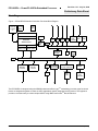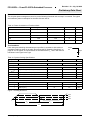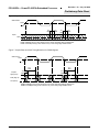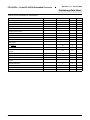
1
Part Number 405EXr
Revision 1.10 - July 10, 2008
405EXr
Preliminary Data Sheet
PowerPC 405EXr Embedded Processor
Features
• AMCC PowerPC® 405 32-bit RISC processor core
operating from 333MHz to 533MHz including
16KB I- and D-caches with parity checking
• On-chip 128-bit processor local bus (PLB)
operating up to 200MHz
• On-chip 32-bit peripheral bus (OPB) operating up
to 100 MHz
• External 8-,16-, or 32-bit peripheral bus (EBC)
operating up to 100MHz
• External bus master (EBM) operating up to
100MHz
• On-chip Security feature with True Random
Number generation
• Eight- and 16-bit NAND Flash interface
• One one-lane PCI Express interfaces operating up
to 2.5 Gbps
• One Gigabit Ethernet interfaces (half- and fullduplex) to external PHY (GMII/MII/RGMII)
• USB 2.0 OTG port configurable as either Host or
Device
• Programmable universal interrupt controller (UIC)
• General Purpose Timer (GPT)
• Up to two serial ports (16750 compatible UART)
• Two IIC interfaces operating up to 400kHz and
supporting all standard IIC EEPROMs
• One SCP (SPI) synchronous full-duplex channel
operating up to 25 MHz
• Inter-chip connectivity (SCP and IIC)
• General purpose I/Os (GPIOs), each with
programmable interrupts and outputs
• Boot from NOR Flash on the external peripheral
bus or NAND Flash on the NAND Flash interface
• Supports JTAG for board-level testing
• DMA (4-channel) support for all on-chip slaves
and external bus, UARTs, and devices on the EBC
• DDR1/2 SDRAM interface operating up to 400
Mbps
• System power management, low power
dissipation and small form factor
• Available in a RoHS compliant (lead-free) package
Description
With speeds up to 533MHz, a flexible off-chip memory
architecture, and a diverse communications package
that includes PCI Express, USB 2.0 OTG, and
10/100/1000 Ethernet, the PowerPC 405EXr
embedded processor provides a low power and small
footprint system-on-a-chip (SOC) solution for a wide
range of high performance, cost-constrained
embedded applications. This includes wireless LAN
applications, security appliances, internet appliances,
line cards, and intelligent USB peripherals. It is an
easily programmable general purpose, 32-bit RISC
controller that offers an upgrade path for applications
AMCC Proprietary
in need of performance and connectivity
improvements.
Technology: Cu-08 CMOS, 90nm
Package: 388-ball, 27mm × 27mm, enhanced plastic
ball grid array (EPBGA), 1mm ball pitch
Power consumption: typically less than 2W at all
speeds
Voltages required: 3.3V, 2.5V, 1.8V (DDR2 SDRAM
only), and 1.2V
1
PPC405EXr – PowerPC 405EXr Embedded Processor
Revision 1.10 - July 10, 2008
Preliminary Data Sheet
Table of Contents
Features . . . . . . . . . . . . . . . . . . . . . . . . . . . . . . . . . . . . . . . . . . . . . . . . . . . . . . . . . . . . . . . . . . . . . . . . . . . . . . . . . 1
Description . . . . . . . . . . . . . . . . . . . . . . . . . . . . . . . . . . . . . . . . . . . . . . . . . . . . . . . . . . . . . . . . . . . . . . . . . . . . . . . 1
Table of Contents . . . . . . . . . . . . . . . . . . . . . . . . . . . . . . . . . . . . . . . . . . . . . . . . . . . . . . . . . . . . . . . . . . . . . . . . . . 2
List of Figures . . . . . . . . . . . . . . . . . . . . . . . . . . . . . . . . . . . . . . . . . . . . . . . . . . . . . . . . . . . . . . . . . . . . . . . . . . . . . 3
List of Tables . . . . . . . . . . . . . . . . . . . . . . . . . . . . . . . . . . . . . . . . . . . . . . . . . . . . . . . . . . . . . . . . . . . . . . . . . . . . . . 4
Ordering, PVR, and JTAG Information . . . . . . . . . . . . . . . . . . . . . . . . . . . . . . . . . . . . . . . . . . . . . . . . . . . . . . . . . . 5
Address Maps . . . . . . . . . . . . . . . . . . . . . . . . . . . . . . . . . . . . . . . . . . . . . . . . . . . . . . . . . . . . . . . . . . . . . . . . . . . . . 7
PowerPC 405 Processor . . . . . . . . . . . . . . . . . . . . . . . . . . . . . . . . . . . . . . . . . . . . . . . . . . . . . . . . . . . . . . . . . . . . . 9
Internal Buses . . . . . . . . . . . . . . . . . . . . . . . . . . . . . . . . . . . . . . . . . . . . . . . . . . . . . . . . . . . . . . . . . . . . . . . . . . . . . 9
External Bus Controller . . . . . . . . . . . . . . . . . . . . . . . . . . . . . . . . . . . . . . . . . . . . . . . . . . . . . . . . . . . . . . . . . . . . . 10
NAND Flash Controller . . . . . . . . . . . . . . . . . . . . . . . . . . . . . . . . . . . . . . . . . . . . . . . . . . . . . . . . . . . . . . . . . . . . . 10
DMA Controller . . . . . . . . . . . . . . . . . . . . . . . . . . . . . . . . . . . . . . . . . . . . . . . . . . . . . . . . . . . . . . . . . . . . . . . . . . . 10
USB 2.0 OTG Interface . . . . . . . . . . . . . . . . . . . . . . . . . . . . . . . . . . . . . . . . . . . . . . . . . . . . . . . . . . . . . . . . . . . . . 11
DDR1/2 SDRAM Controller . . . . . . . . . . . . . . . . . . . . . . . . . . . . . . . . . . . . . . . . . . . . . . . . . . . . . . . . . . . . . . . . . . 11
PCI Express . . . . . . . . . . . . . . . . . . . . . . . . . . . . . . . . . . . . . . . . . . . . . . . . . . . . . . . . . . . . . . . . . . . . . . . . . . . . . 12
Security Function . . . . . . . . . . . . . . . . . . . . . . . . . . . . . . . . . . . . . . . . . . . . . . . . . . . . . . . . . . . . . . . . . . . . . . . . . 12
UART . . . . . . . . . . . . . . . . . . . . . . . . . . . . . . . . . . . . . . . . . . . . . . . . . . . . . . . . . . . . . . . . . . . . . . . . . . . . . . . . . . 13
IIC Bus Interface . . . . . . . . . . . . . . . . . . . . . . . . . . . . . . . . . . . . . . . . . . . . . . . . . . . . . . . . . . . . . . . . . . . . . . . . . . 14
Serial Communication Port Interface (SCP/SPI) . . . . . . . . . . . . . . . . . . . . . . . . . . . . . . . . . . . . . . . . . . . . . . . . . . 14
General Purpose I/O (GPIO) Controller . . . . . . . . . . . . . . . . . . . . . . . . . . . . . . . . . . . . . . . . . . . . . . . . . . . . . . . . 15
Universal Interrupt Controller (UIC) . . . . . . . . . . . . . . . . . . . . . . . . . . . . . . . . . . . . . . . . . . . . . . . . . . . . . . . . . . . . 15
Ethernet Controller . . . . . . . . . . . . . . . . . . . . . . . . . . . . . . . . . . . . . . . . . . . . . . . . . . . . . . . . . . . . . . . . . . . . . . . . 15
JTAG . . . . . . . . . . . . . . . . . . . . . . . . . . . . . . . . . . . . . . . . . . . . . . . . . . . . . . . . . . . . . . . . . . . . . . . . . . . . . . . . . . . 16
Signal Lists . . . . . . . . . . . . . . . . . . . . . . . . . . . . . . . . . . . . . . . . . . . . . . . . . . . . . . . . . . . . . . . . . . . . . . . . . . . . . . 18
Signal Functional Descriptions . . . . . . . . . . . . . . . . . . . . . . . . . . . . . . . . . . . . . . . . . . . . . . . . . . . . . . . . . . . . . . . 41
Ratings and Specifications . . . . . . . . . . . . . . . . . . . . . . . . . . . . . . . . . . . . . . . . . . . . . . . . . . . . . . . . . . . . . . . . . . 48
Spread Spectrum Clocking . . . . . . . . . . . . . . . . . . . . . . . . . . . . . . . . . . . . . . . . . . . . . . . . . . . . . . . . . . . . . . . . . . 56
DDR 2/1 SDRAM I/O Specifications . . . . . . . . . . . . . . . . . . . . . . . . . . . . . . . . . . . . . . . . . . . . . . . . . . . . . . . . . . . 62
PCI Express (PCI-E) I/O Specifications . . . . . . . . . . . . . . . . . . . . . . . . . . . . . . . . . . . . . . . . . . . . . . . . . . . . . . . . 70
Initialization . . . . . . . . . . . . . . . . . . . . . . . . . . . . . . . . . . . . . . . . . . . . . . . . . . . . . . . . . . . . . . . . . . . . . . . . . . . . . . 72
2
AMCC Proprietary
PPC405EXr – PowerPC 405EXr Embedded Processor
Revision 1.10 - July 10, 2008
Preliminary Data Sheet
List of Figures
Figure 1. PPC405EXr Embedded Controller Functional Block Diagram . . . . . . . . . . . . . . . . . . . . . . . . . . . . . . . . . 6
Figure 2. Package 27mm, 388-Ball EPBGA . . . . . . . . . . . . . . . . . . . . . . . . . . . . . . . . . . . . . . . . . . . . . . . . . . . . . 17
Figure 3. Clocking Waveform . . . . . . . . . . . . . . . . . . . . . . . . . . . . . . . . . . . . . . . . . . . . . . . . . . . . . . . . . . . . . . . . 55
Figure 4. Input Setup and Hold Timing Waveform . . . . . . . . . . . . . . . . . . . . . . . . . . . . . . . . . . . . . . . . . . . . . . . . 58
Figure 5. Output Delay and Float Timing Waveform . . . . . . . . . . . . . . . . . . . . . . . . . . . . . . . . . . . . . . . . . . . . . . . 58
Figure 6. Input Setup and Hold Timing Waveform for RGMII Signals . . . . . . . . . . . . . . . . . . . . . . . . . . . . . . . . . . 59
Figure 7. Output Delay and Hold Timing Waveform for RGMII Signals . . . . . . . . . . . . . . . . . . . . . . . . . . . . . . . . 59
Figure 8. DDR SDRAM Simulation Signal Termination Model . . . . . . . . . . . . . . . . . . . . . . . . . . . . . . . . . . . . . . . 62
Figure 9. DDR SDRAM Write Cycle Timing . . . . . . . . . . . . . . . . . . . . . . . . . . . . . . . . . . . . . . . . . . . . . . . . . . . . . 64
Figure 10. DDR SDRAM Read Data Path for a Single Data Bit . . . . . . . . . . . . . . . . . . . . . . . . . . . . . . . . . . . . . . 67
Figure 11. DDR SDRAM Memory Data and DQS . . . . . . . . . . . . . . . . . . . . . . . . . . . . . . . . . . . . . . . . . . . . . . . . . 68
Figure 12. DDR SDRAM Read Cycle Timing—Example . . . . . . . . . . . . . . . . . . . . . . . . . . . . . . . . . . . . . . . . . . . 69
AMCC Proprietary
3
PPC405EXr – PowerPC 405EXr Embedded Processor
Revision 1.10 - July 10, 2008
Preliminary Data Sheet
List of Tables
Table 1. System Memory Address Map (4GB System Memory) . . . . . . . . . . . . . . . . . . . . . . . . . . . . . . . . . . . . . . 7
Table 2. DCR Address Map . . . . . . . . . . . . . . . . . . . . . . . . . . . . . . . . . . . . . . . . . . . . . . . . . . . . . . . . . . . . . . . . . . 8
Table 3. Signals Listed Alphabetically . . . . . . . . . . . . . . . . . . . . . . . . . . . . . . . . . . . . . . . . . . . . . . . . . . . . . . . . . 18
Table 4. Signals Listed by Ball Assignment . . . . . . . . . . . . . . . . . . . . . . . . . . . . . . . . . . . . . . . . . . . . . . . . . . . . . 32
Table 5. Pin Groups . . . . . . . . . . . . . . . . . . . . . . . . . . . . . . . . . . . . . . . . . . . . . . . . . . . . . . . . . . . . . . . . . . . . . . . 39
Table 6. Non-Functional Ball Connections . . . . . . . . . . . . . . . . . . . . . . . . . . . . . . . . . . . . . . . . . . . . . . . . . . . . . . 40
Table 7. Signal Functional Description . . . . . . . . . . . . . . . . . . . . . . . . . . . . . . . . . . . . . . . . . . . . . . . . . . . . . . . . . 41
Table 8. Absolute Maximum Ratings . . . . . . . . . . . . . . . . . . . . . . . . . . . . . . . . . . . . . . . . . . . . . . . . . . . . . . . . . . 48
Table 9. Package Thermal Specifications . . . . . . . . . . . . . . . . . . . . . . . . . . . . . . . . . . . . . . . . . . . . . . . . . . . . . . . 49
Table 10. Recommended DC Operating Conditions . . . . . . . . . . . . . . . . . . . . . . . . . . . . . . . . . . . . . . . . . . . . . . . 50
Table 11. I/O Input Capacitance . . . . . . . . . . . . . . . . . . . . . . . . . . . . . . . . . . . . . . . . . . . . . . . . . . . . . . . . . . . . . . 52
Table 12. Typical DC Power Supply Requirements with DDR1 SDRAM . . . . . . . . . . . . . . . . . . . . . . . . . . . . . . . 52
Table 13. Maximum DC Power Supply Requirements with DDR1 SDRAM . . . . . . . . . . . . . . . . . . . . . . . . . . . . . 52
Table 14. Typical DC Power Supply Requirements with DDR2 SDRAM . . . . . . . . . . . . . . . . . . . . . . . . . . . . . . . 53
Table 15. Maximum DC Power Supply Requirements with DDR2 SDRAM . . . . . . . . . . . . . . . . . . . . . . . . . . . . . 53
Table 16. DC Power Supply Loads with DDR1 SDRAM . . . . . . . . . . . . . . . . . . . . . . . . . . . . . . . . . . . . . . . . . . . . 54
Table 17. DC Power Supply Loads with DDR2 SDRAM . . . . . . . . . . . . . . . . . . . . . . . . . . . . . . . . . . . . . . . . . . . . 54
Table 18. Power Contribution of Functional Units . . . . . . . . . . . . . . . . . . . . . . . . . . . . . . . . . . . . . . . . . . . . . . . . . 55
Table 19. System Clocking Specifications . . . . . . . . . . . . . . . . . . . . . . . . . . . . . . . . . . . . . . . . . . . . . . . . . . . . . . 55
Table 20. Peripheral Interface I/O Clock Timings (not SDRAM or PCI-E) . . . . . . . . . . . . . . . . . . . . . . . . . . . . . . 57
Table 21. I/O Specifications . . . . . . . . . . . . . . . . . . . . . . . . . . . . . . . . . . . . . . . . . . . . . . . . . . . . . . . . . . . . . . . . . 60
Table 22. DDR SDRAM Output Driver Specifications . . . . . . . . . . . . . . . . . . . . . . . . . . . . . . . . . . . . . . . . . . . . . . 63
Table 23. DDR SDRAM Write Operation Conditions . . . . . . . . . . . . . . . . . . . . . . . . . . . . . . . . . . . . . . . . . . . . . . 63
Table 24. I/O Timing—DDR SDRAM TDS . . . . . . . . . . . . . . . . . . . . . . . . . . . . . . . . . . . . . . . . . . . . . . . . . . . . . . . 64
Table 25. I/O Timing—DDR SDRAM TSA and THA . . . . . . . . . . . . . . . . . . . . . . . . . . . . . . . . . . . . . . . . . . . . . . . . 65
Table 26. I/O Timing—DDR SDRAM Write Timing TSD and THD . . . . . . . . . . . . . . . . . . . . . . . . . . . . . . . . . . . . . 65
Table 27. I/O Timing—DDR SDRAM Read Timing TSD and THD . . . . . . . . . . . . . . . . . . . . . . . . . . . . . . . . . . . . . 68
Table 28. PCI-E Receiver I/O Specifications . . . . . . . . . . . . . . . . . . . . . . . . . . . . . . . . . . . . . . . . . . . . . . . . . . . . 70
Table 29. PCI-E Reference Clock I/O Specifications . . . . . . . . . . . . . . . . . . . . . . . . . . . . . . . . . . . . . . . . . . . . . . 70
Table 30. PCI-E Transmitter I/O Specifications . . . . . . . . . . . . . . . . . . . . . . . . . . . . . . . . . . . . . . . . . . . . . . . . . . 71
Table 31. Strapping Pin Assignments . . . . . . . . . . . . . . . . . . . . . . . . . . . . . . . . . . . . . . . . . . . . . . . . . . . . . . . . . . 72
4
AMCC Proprietary
Revision 1.10 - July 10, 2008
PPC405EXr – PowerPC 405EXr Embedded Processor
Preliminary Data Sheet
Ordering, PVR, and JTAG Information
This section provides the part number nomenclature. For availability, contact your local AMCC sales office.
Order Part Number
(see Notes:)
Package
Rev
Level
PVR Value
JTAG ID
PPC405EXr
PPC405EXr-SpCfffT
27mm, 388-ball, EPBGA
C
0x1291147B
0x1405B1E1
PPC405EXr
PPC405EXr-NpCfffT
27mm, 388-ball, EPBGA
C
0x12911479
0x1405B1E1
Product Name
Notes:
1.
2.
3.
4.
S = security feature present, N = security feature not present
p = Package: S = lead-free (RoHS compliant), P = leaded
C = Chip revision level C
fff = Processor frequency
333 = 333MHz
400 = 400MHz
533 = 533MHz
5. T = Case temperature range, -40°C to +85°C (see footnote 5. on page 51)
The part number contains a part modifier. Included in the modifier is a revision code. This refers to the die mask
revision number and is specified in the part numbering scheme for identification purposes only.
The PVR (Processor Version Register) and the JTAG ID register are software accessible (read-only) and contain
information that uniquely identifies the part. See the PPC405EXr Embedded Processor User’s Manual for details
about accessing these registers.
Order Part Number Key
PPC405EXr-SSB533T
AMCC Part Number
Security
Chip Package
Case Temperature Range
Processor Speed (MHz)
Revision Level
Note: The example P/N above has the security feature, is lead-free, capable of running at 533MHz,
and is shipped in a tray (tape-and-reel packaging is not available).
AMCC Proprietary
5
PPC405EXr – PowerPC 405EXr Embedded Processor
Revision 1.10 - July 10, 2008
Preliminary Data Sheet
Block Diagram
Figure 1. PPC405EXr Embedded Controller Functional Block Diagram
Universal
Interrupt
Controller
x3
Clock
Control
Reset
Power
Mgmt
Timers
MMU
DCRs
Power PC
405 Processor
JTAG
Trace
UART
x2
DCR
IICx2/
BSC
SCP
(SPI)
GPIO
NAND
Flash
Controller
EBC
EBM
Arbiter
Bus
On-chip Peripheral Bus (OPB)
16KB D-Cache 16KB I-Cache
OPB/PLB
Bridges
GPT
PKA
TRNG
Processor Local Bus (PLB4)—128 bits
Arbiter
DDR1/2
SDRAM
Controller
EIP-94
Security
Feature
PCI-E
1-lane
HSS
DMA
Controller
(4-Channel)
MAL/w
Interrupt Coalescing
AHB-PLB
Bridge
Ethernet
MAC
1Gbit
USB 2.0
OTG
Controller
ULPI
The PPC405EXr is designed using the IBM Microelectronics Blue LogicTM methodology in which major functional
blocks are integrated together to create an ASIC (application-specific integrated circuit) product. This approach
provides a consistent way to create complex ASICs using IBM CoreConnectTM Bus Architecture.
6
AMCC Proprietary
Revision 1.10 - July 10, 2008
PPC405EXr – PowerPC 405EXr Embedded Processor
Preliminary Data Sheet
Address Maps
The PPC405EXr incorporates two address maps. The first address map defines the possible use of addressable
memory regions that the processor can access. The second address map defines Device Configuration Register
(DCR) addresses (numbers). The DCRs are accessed by software running on the PPC405EXr processor through
the use of mtdcr and mfdcr instructions.
Table 1. System Memory Address Map (4GB System Memory)
Function
Local Memory
Subfunction
DDR 2/1 SDRAM
Start Address (Hex)
End Address (Hex)
Size
0 0000 0000
0 7FFF FFFF
2GB
EBC
0 8000 0000
0 8FFF FFFF
256MB
PCI Express
0 9000 0000
0 EF5F FFFF
1.5GB
GPT
0 EF60 0000
0 EF60 01FF
512B
UART 0
0 EF60 0200
0 EF60 0207
8B
Reserved
0 EF60 0208
0 EF60 02FF
248B
UART 1
0 EF60 0300
0 EF60 0307
8B
Reserved
0 EF60 0308
0 EF60 03FF
248B
IIC 0
0 EF60 0400
0 EF60 041F
32B
Reserved
0 EF60 0420
0 EF60 04FF
224B
IIC 1
0 EF60 0500
0 EF60 051F
32B
Reserved
0 EF60 0520
0 EF60 05FF
224B
SCP
0 EF60 0600
0 EF60 0605
6B
Reserved
0 EF60 0606
0 EF60 06FF
250B
OPB Arbiter
0 EF60 0700
0 EF60 073F
64B
Reserved
0 EF60 0740
0 EF60 07FF
192B
GPIO
0 EF60 0800
0 EF60 087F
128B
Reserved
0 EF60 0880
0 EF60 08FF
128B
Ethernet 0
0 EF60 0900
0 EF60 09FF
256B
Reserved
0 EF60 0A00
0 EF60 0AFF
256B
RGMII Bridge
0 EF60 0B00
0 EF60 0C03
260B
OPB Peripherals
PLB/AHB Peripherals
EBC
Reserved
0 EF60 0C04
0 EF60 FFFF
62KB
PKA +TRNG
0 EF61 0000
0 EF61 FFFF
64KB
PCI Express Interrupt Handler
0 EF62 0000
0 EF62 00FF
256B
Reserved
0 EF62 0100
0 EF6B FFFF
640KB
USB OTG
0 EF6C 0000
0 EF6F FFFF
256KB
Security
0 EF70 0000
0 EF77 FFFF
512KB
Reserved
0 EF78 0000
0 EFFF FFFF
8.9MB
EBC Memory
0 F000 0000
0 FFDF FFFF
254MB
EBC Memory—Boot ROM
0 FFE0 0000
0 FFFF FFFF
2MB
Notes:
1. If peripheral bus boot is selected, peripheral bank 0 is automatically configured at reset to the address range listed above.
2. After the boot process, software may reassign the boot memory regions for other uses.
3. PCI Express can use PLB address range 0x1 0000 0000 to 0xF FFFF FFFF even though the CPU can not access it.
AMCC Proprietary
7
PPC405EXr – PowerPC 405EXr Embedded Processor
Revision 1.10 - July 10, 2008
Preliminary Data Sheet
Table 2. DCR Address Map
Function
Total DCR Address Space1
Start Address (Hex)
End Address (Hex)
Size
0x000
0x3FF
1KW (4KB)1
Reserved
000
00B
CPR (Clocking Power-on Reset)
00C
00D
2W
System DCRs
00E
00F
2W
DDR 2/1 SDRAM Controller
010
011
2W
External Bus Controller (EBC)
012
013
2W
External Bus Master (EBM)
014
015
2W
Reserved
016
01F
PLB4XAHB Bridge
020
02F
16W
Reserved
030
03F
PCI Express 0
040
05F
Reserved
060
07F
PLB4 Arbiter
080
08F
16W
32W
PLB-to-OPB Bridge
090
09F
16W
OPB-to-PLB Bridge
0A0
0A7
8W
Reserved
0A8
0AF
Power Management
0B0
0B2
3W
Reserved
0B3
0BF
UIC 0
0C0
0CF
16W
UIC 1
0D0
0DF
16W
UIC 2
0E0
0EF
16W
Reserved
0F0
0FF
DMA
100
13F
Reserved
140
17F
Ethernet MAL
180
1FF
Reserved
200
3FF
64W
128W
Notes:
1. A DCR address is 10 bits (1024 or 1K unique addresses). Each unique address represents a single 32-bit (word) register, or one kiloword
(KW) (which equals 4KB).
8
AMCC Proprietary
Revision 1.10 - July 10, 2008
PPC405EXr – PowerPC 405EXr Embedded Processor
Preliminary Data Sheet
PowerPC 405 Processor
The PPC405 processor is a fixed-point, 32-bit RISC unit.
Features include:
• Five-stage pipeline with single-cycle execution of most instructions, including loads and stores
• Separate, configurable 16 KB D- and I-caches, both two-way set associative
• Thirty-two 32-bit general purpose registers (GPRs)
• Unaligned load/store support
• Hardware multiply/divide
• Parity detection and reporting for the instruction cache, data cache, and translation look-aside buffer (TLB)
• Double word instruction fetch from cache
• Translation of the four GB logical address space into physical addresses
• Built-in timer and debug support
• Power management
• DCR interface is 32 bits wide
• Selectable processor vs. bus clock ratios (N:1 ratio only, where N =1, 2, 3,or 4 )
Internal Buses
The PPC405EXr contains four internal buses: the processor local bus (PLB), the Advanced High-Performance Bus
(AHB), the on-chip peripheral bus (OPB), and the device control register (DCR) bus. High performance devices
such as the processor, the DDR SDRAM memory controller, PCI Express, the Ethernet MAL, and DMA utilize the
PLB. Lower bandwidth I/O interfaces such as communications and timer interfaces utilize the OPB. The daisychained DCR bus provides a lower bandwidth path for passing status and control information between the
processor and the other on-chip peripheral functions.
PLB
The Processor Local Bus (PLB) is a high-performance on-chip bus used to connect PLB-equipped master and
slave devices to the PPC405 CPU. It provides a 128-bit data path with 64-bit addressing and operates up to
200MHz. There are bridges between the PLB and the OPB.
Features include:
• Separate and simultaneous 6.4GB/s read and write data paths
• Decoupled address and data buses
• Address pipelining
• Late master request abort capability
• Hidden (overlapped) bus request/grant protocol
• Bus arbitration-locking mechanism
• Byte-enable capability allows for unaligned half word transfers and 3-B transfers
• Support for 32- and 64-B burst transfers
• Read word address capability
• Sequential burst protocol
• Guarded and unguarded memory transfers
• Simultaneous control, address, and data phases
• DMA buffered, flyby, peripheral-to-memory, memory-to-peripheral, and DMA memory-to-memory operations
AHB
The Advanced High-Performance Bus (AHB) is dedicated to the USB OTG 2.0.
Features include:
• 32-bit data path
• 32-bit address
• Synchronous to the PLB
• From 60MHz to 100MHz.
AMCC Proprietary
9
PPC405EXr – PowerPC 405EXr Embedded Processor
Revision 1.10 - July 10, 2008
Preliminary Data Sheet
OPB
The OPB provides 32-bit address and data interfaces, and operates up to 100MHz. There are bridges between the
OPB and the PLB.
Features include:
• Pipelined read support
• Dynamic bus sizing
• Single-cycle data transfer between masters and slaves
DCR Bus
The daisy-chained DCR bus provides a path for passing status and control information between the processor core
and the other on-chip cores. All DCRs are 32 bits in width with 10-bit addressing.
External Bus Controller
The external bus controller (EBC and EBM) transfers data between the PLB and external memory or peripheral
devices attached to the external peripheral bus. The EBC provides direct attachment of memory devices such as
ROM and SRAM, DMA device paced memory devices, and DMA peripheral devices.
Features include:
• Up to 33MHz to 100 MHz speed
• Data bus is 8, 16, or 32 bits with a 27-bit address bus
• Up to four chip selects
• Arbitration and multi-master supported
• Flash ROM interface
• Boot from 8- or 16-bit NOR flash support
• Direct support for 8-,16-, or 32-bit SRAM and external peripherals
• External bus master support
NAND Flash Controller
The NAND Flash controller (NDFC) provides a simple interface between the External Bus Controller (EBC) and a
variety of NAND Flash-based storage devices.
Features include:
• Attachment as internal EBC slave device
• Eight- and 16-bit NAND Flash interface
• Up to four banks of NAND Flash supported
• Device sizes:
– 4MB and larger supported for read/write access
– 4MB to 256MB supported for boot-from-NAND flash (size supported depends on addressing mode)
• 512B + 16B or 2kB + 64B device page sizes supported
• ECC generation - hamming code, single-bit correction, double-bit detection (SEC/DED)
• Eight-bit command write, address write, and data read/write
• Interrupt on device ready (after long page write or block erase operations)
• Boot from NAND
– Executes up to 4KB of boot code out of first block
– Automatic page read accesses performed based on device configuration and read address
DMA Controller
The Direct Memory Access (DMA) controller is a Processor Local Bus (PLB) master that enables faster data
transfer between memory and peripherals than is possible under program control. The 4-channel DMA controller
handles data transfers between memory and peripherals and from memory-to-memory. Each channel has an
10
AMCC Proprietary
Revision 1.10 - July 10, 2008
PPC405EXr – PowerPC 405EXr Embedded Processor
Preliminary Data Sheet
independent set of registers needed for data transfer: a control register, a source address register, a destination
address register, and a transfer count register.
Features include:
• Memory-to-memory transfers
• Buffered memory-to-peripheral transfers
• Buffered peripheral-to-memory transfers
• Four independent DMA channels
• Scatter/gather capability for dynamically programming multiple DMA transfers
• Programmable address increment or decrement
• Internal data buffering
• Can transfer data to/from any PLB slave, including the external bus
USB 2.0 OTG Interface
One USB 2.0 On-the-Go (OTG) controller that can be configured as either a Host or Device port.
Features include:
• Low- (Host only), Full- and High-Speed support
• Internal DMA to optimize performance and offload the CPU
• Up to two IN/OUT Endpoints in Device mode (one can be isochronous)
• Supports maximum packet size of 1024B (isochronous) and 512B (bulk)
• Support for isochronous traffic
• Three packets per microframe (24MB/s throughput)
• Eight KB buffer
• ULPI SDR interface
DDR1/2 SDRAM Controller
The Double Data Rate 1/2 (DDR1/2) SDRAM memory controller supports industry standard discrete devices that
are compatible with both the DDR1 or DDR2 specifications. The correct I/O supply voltage must be provided for the
two types of DDR devices: DDR1 devices require +2.5V and DDR2 devices require +1.8V.
Global memory timings, address and bank sizes, and memory addressing modes are programmable.
Features include:
• 16- or 32-bit memory interface
• Optional 8-bit error checking and correcting (ECC)
• 1.6-GB/s peak data rate
• Two memory banks of up to 1 GB each
• Maximum capacity of 2GB
• Support for one memory bank of 2GB with CAS latencies of 2, 2.5, or 3
• Clock frequencies from 133MHz (266Mbps) to 200MHz (400Mbps) supported
(Faster parts may be used, but must be clocked no faster than 200MHz)
• Page mode accesses (up to 16 open pages) with configurable paging policy
• Programmable address mapping and timing
• Software initiated self-refresh
• Power management (self-refresh, suspend)
• Two regions (two chip selects, one clock driver)
AMCC Proprietary
11
PPC405EXr – PowerPC 405EXr Embedded Processor
Revision 1.10 - July 10, 2008
Preliminary Data Sheet
PCI Express
The PCI Express single-lane interface include the following features:
Features include:
• Compliant with PCI Express base specification 1.1
• Port can be End Point or Root Complex. (Upstream & Downstream)
• PCI-Express to PCI-Express opaque (Non-Transparent) bridge
• Power Management
• Supports one virtual channel (VC0) with no Traffic Class (TC) filtering
• Maximum Payload block size 256B
• Supports up to 512B maximum Read request size
• Requests supported:
– Up to two posted outbound Write requests (memory and messages)
– Up to two posted inbound Write requests
– Up to two outbound Read requests outstanding on PCI Express
– Up to two inbound Read requests outstanding on PCI Express
– Outbound I/O request as a PCI Express Root Port
– Inbound I/O request as a PCI Express End Point
• Buffering in PCI Express Port for the following transaction types:
– 1KB Replay buffer: up to eight in flight transactions
– 512B for Outbound posted Writes
– 512B for Outbound Reads completion
– 512B for Inbound posted Writes
– 512B for Inbound Reads completion
• Parity checking on each buffer
• POM Programmable Outbound Memory Regions: 3 Memory, 1 I/O, 1 Message, 1 config, 1 Internal Regs
• PIM Programmable Inbound Memory Regions: 4 Memory, 1 I/O, 1 Expansion ROM
• INTx Interrupts support (PCI legacy):
– Up to four INTx Termination for Root Ports. A/B/C/D interrupts are wired to the UIC
– A/B/C/D INTx types Generation for Endpoints
• MSI - Message Signaled Interrupts
– MSI Generation for End Point
– MSI Termination for Root Ports
– MSI_X Termination for Root Ports
Security Function
The built-in security function is a cryptographic engine attached to the 128-bit PLB with built-in DMA and interrupt
controllers.
Features include:
• Federal Information Processing Standard (FIPS) 140-2 design
• Support for an unlimited number of Security Associations (SA)
• Different SA formats for each supported protocol (IPsec, SSL/TLS/DTLS, MACSec, SGT L2/L3 and sRTP)
• Internet Protocol Security (IPSec) features
– Full packet transforms (ESP & AH)
– Complete header and trailer processing (IPv4 and IPv6)
– Multi-mode automatic padding
– "Mutable bit" handler for AH, including IPv4 option and IPv6 extension headers
• Secure Socket Layer (SSL), Transport Layer Security (TLS), and Datagram Transport Layer Security (DTLS)
– Packet transforms
– One-pass hash-then-encrypt or decrypt-then-hash for SSL, TLS and DTLS packet transforms using ARC4
Stream Cipher
12
AMCC Proprietary
PPC405EXr – PowerPC 405EXr Embedded Processor
Revision 1.10 - July 10, 2008
Preliminary Data Sheet
• Secure Real-Time Protocol (sRTP) features
– Packet transforms
– ROC removal and TAG insertion
– Variable bypass offset of header length per packet
• Media Access Control Security (MACSec) features
– Cipher suite GCM-AES-128
– Header insertion and removal
– Integrity and confidentiality with MSDU
• SGT L2 supported features:
– GCM-AES with 128-bit key.
– Integrity only and with confidentiality of MSDU
• ICV generation and validation SGT L3 supported features
– AES-GCM, AES-GMAC with 128, 192 and 256 bit key.
• IPsec/SSL security acceleration engine
• DES, 3DES, AES, ARC-4, AES-GCM, and GMAC-AES encryption/decryption
• MD-5, SHA-1, and SHA-256 hashing
• Public key acceleration for RSA, DSA and Diffie-Hellman
• Combined encryption-hash and hash-decryption with the AES-CCM algorithm.
• True or pseudo random number generators
– Non-deterministic true random numbers
– Pseudo random numbers with lengths of 8B or 16B
– ANSI X9.17 Annex C compliant using a DES algorithm
• Interrupt controller
– Fifteen programmable, maskable interrupts
– Initiate commands via an input interrupt
– Sixteen programmable interrupts indicating completion of certain operations
– All interrupts mapped to one level- or edge-sensitive programmable interrupt output
• DMA controller
– Autonomous, 4-channel
– 1024-words (32 bits/word) per DMA transfer
– Scatter/gather capability with byte aligned addressing
– Byte reverse capability on SA and descriptors
UART
The Universal Asynchronous Receiver/Transmitter (UART) interface provides four configurations:
• One 8-signal port
• Two 4-signal ports.
• Two 2-signal ports
• One 4-signal port and one 2-signal port
The UART performs serial-to-parallel conversion on data received from a peripheral device or a modem, and
parallel-to-serial conversion on data received from the processor.
Features include:
• Compatible with the16750
• All six software modem control functions (CTS, RTS, DSR, DTR, RI, DCD) on UART0
• Programmable auto flow (data flow controlled by RTS and CTS signals)
• Characters can be 5, 6, 7, or 8 bits
• Programmable start, stop, parity bit insertion
• Sixty-four byte FIFOs for buffering Tx and Rx data
• LIN sub-bus specification compliant - line break generation/detection and false start bit detection
• Programmable internal/external loopback capabilities
• Low Power and Sleep mode
• Register conformance (after reset) to configuration of the NS16450 register set
AMCC Proprietary
13
PPC405EXr – PowerPC 405EXr Embedded Processor
Revision 1.10 - July 10, 2008
Preliminary Data Sheet
• Hold and shift registers (eliminate need for precise synchronization between processor and serial data in
character mode)
• Complete status reporting
• Full prioritized interrupt system controls
• Independently controlled transmit, receive, line status, and data set interrupts
• Programmable baud generator (divides serial clock input and generates 16x clock)
• Ability to add/delete standard asynchronous communication bits such as start, stop, and parity to/from serial
data
• Even, odd, or no-parity bit generation and detection
• Stop bit generation of 1, 1.5, or 2 bits
• Variable baud rate
• Internal diagnostic capability
• Loopback controls for isolating communications link faults
• Break, parity, overrun, framing error simulation
• OPB interface with optional DMA support
IIC Bus Interface
The Inter-Integrated Circuit (IIC) interface provides a Philips I2C® compatible interface operating up to 400kHz
either as a master, a slave, or both with a bootstrap controller (BSC) included. During chip reset, the bootstrap
controller can read configuration data from an IIC compatible memory device (e.g., EEPROM). This data can be
used to replace the default configuration settings provided by the chip.
Features include:
• Two IIC channels
• Compliant with Philips Semiconductors I2C Specification, dated 1995
• Operation at 100kHz or 400kHz
• Byte (8-bit) data
• Addresses are 10 or 7 bits
• Slave Transmit and Receive
• Master Transmit and Receive
• Multiple bus masters supported
• Programmable as master, slave, or master/slave
• Boot parameters read from IIC attached memory (Port 0) with IIC bootstrap controller
• OPB slave interface is 32 bits wide
Serial Communication Port Interface (SCP/SPI)
The Serial Communication Port (SCP) (also known as the Serial Peripheral Interface or SPI) is a full-duplex,
synchronous, character-oriented (byte) port that allows the exchange of data with other serial devices. The SCP is
a master on the serial port supporting a three-wire interface (receive, transmit, and clock), and is a slave on the
OPB.
Features include:
• One SCP channel, full duplex synchronous
• SCP master
• Up to 25MHz
• Programmable internal loopback capabilities
• Multi-master protocol supported
• Independent masking of all interrupts (master collision, transmit FIFO overflow, transmit FIFO empty, receive
FIFO full, receive FIFO underflow, receive FIFO overflow)
• Dynamic control of serial bit rate of data transfer (serial-master mode only)
• Data Item size for each data transfer under programmer control (4-to-16 bits)
• OPB slave interface is 32 bits wide
14
AMCC Proprietary
PPC405EXr – PowerPC 405EXr Embedded Processor
Revision 1.10 - July 10, 2008
Preliminary Data Sheet
General Purpose I/O (GPIO) Controller
The GPIO controller enables multiplexing of module I/O pins with multiple functions within the chip. That is, a single
package pin can be assigned to multiple I/O functions. Which function the pin is assigned to is determined by
register bit settings controlled by software. This significantly reduces the number of package pins needed to
support multiple I/O groups.
Features include:
• Up to 32 GPIOs available
– GPIOs are multiplexed with alternate functions
– If not in use for dedicated functions, I/Os are available as GPIOs
• Direct control of all functions from registers programmed by means of OPB bus master accesses
• Time multiplexing of controller outputs to module outputs
• Programmable conversion of module outputs to open-drain outputs (enables sharing of active low outputs
externally)
• Time multiplexing of module inputs to controller inputs
Universal Interrupt Controller (UIC)
The Universal Interrupt Controller (UIC) provides the control, status, and communications necessary between the
various sources of interrupts and the PPC405 processor.
Features include:
• Ten external interrupt sources supported
• Generate interrupt on level (high or low) or edge (rising or falling)
• Programmable as synchronous (edge-capture or level-sensitive) or asynchronous (edge- or level-sensitive
triggering)
• Each interrupt source/bit programmable as critical or non critical
• DCR bus interface is 32 bits wide
• Optional interrupt handler vector generation
– Programmable vector base address
– Programmable vector offset size
– Programmable interrupt priority ordering
• Programmable polarity for all interrupt types
• Interrupts of the same type do not need to be in contiguous bit positions
• Status registers provide: current state of all interrupts, current state of enabled interrupts
Ethernet Controller
The Ethernet support provides one 10/100/1000 Mbps interfaces (GMII/MII/RGMII ).
Features include:
• ANSI/IEEE Std. 802.3 and IEEE 802.3u supplement compliant
• Half-duplex and full-duplex support for the following:
– One Gigabit Media Independant Interface (GMII)
– One Media Independant Interface (MII)
– One Reduced GMII interfaces (RGMII)
• Receive and transmit FIFOs are 16K bytes with programmable thresholds
• FCS control for transmit/receive packets
• Multiple packet handling in transmit and receive FIFOs
• Unicast, multicast, broadcast, and promiscuous address filtering
• Two 256-bit hash filters for unicast and multicast frames
• Automatic retransmission of collided frames
• Runt frame rejection
• Programmable inter-frame gap
AMCC Proprietary
15
PPC405EXr – PowerPC 405EXr Embedded Processor
Revision 1.10 - July 10, 2008
Preliminary Data Sheet
• IEEE 802.3x compliant for frame-based flow control mechanism, including self-assembled control frame
transmitting)
• Wake-on-LAN and Power-over-Internet supported
• Programmable internal/external loopback capabilities
• OPB slave (MAC) and PLB master (MAL) interfaces for control and configuration are 32 bits wide
• MAL has 128-bit PLB master interface for data path.
• Extensive error/status vector generation for each processed packet
• VLAN tag ID supported (according to IEEE Draft 802.3ac/D1.0 standard)
• Programmable automatic source address inclusion/replacement for transmit packets
• Programmable automatic Pad/FCS stripping for receive packets
• Programmable VLAN Tag inclusion/replacement for transmit packets
• Half- or full-duplex GMII/RGMII
• Jumbo frames support
• Memory Access Layer (MAL) provides DMA capability to Ethernet channel
• Interrupt coalescence support for two transmit and two receive channels
General Purpose Timer (GPT)
The GPT provides a time base counter and system timers in addition to those defined in the processor.
Features include:
• 32-bit time base counter driven by the OPB clock
• Seven 32-bit compare timers
JTAG
Features include:
• IEEE 1149.1 test access port
• JTAG Boundary Scan Description Language (BSDL)
Refer to http://www.amcc.com/Embedded/Partners for a list of AMCC partners supplying probes for use with the
JTAG interface.
16
AMCC Proprietary
PPC405EXr – PowerPC 405EXr Embedded Processor
Revision 1.10 - July 10, 2008
Preliminary Data Sheet
Figure 2. Package 27mm, 388-Ball EPBGA
Gold Gate Release
Corresponds to
A01 Ball Location
Top View
Logo View
®
Part Number
PPC405EXr
Lot Number
1YWWBZZZZZ
Side View
Epoxy Mold
Compound
2.65 max
PCB
Substrate
0.3 min
27.0
Bottom View
27.0
25.0
AF
AE
AD
AC
AB
AA
Y
W
V
U
T
R
P
N
M
L
K
J
H
G
F
E
D
C
B
A
1.0 Basic
01 03 05 07 09 11 13 15 17 19 21 23 25
02 04 06 08 10 12 14 16 18 20 22 24 26
Notes: 1. All dimensions are in mm.
2. Package conforms to JEDEC MS-034C
3. Package available in leaded or lead-free versions
0.60 ± 0.1 SOLDERBALL x 388
AMCC Proprietary
17
PPC405EXr – PowerPC 405EXr Embedded Processor
Revision 1.10 - July 10, 2008
Preliminary Data Sheet
Signal Lists
The following table lists all the external signals in alphabetical order and shows the ball (pin) number on which the
signal appears. Shared signals are shown with the default signal (following reset) not in brackets and the alternate
signal in brackets. Signals that have different functions for different modes with the same function are separated by
commas.
Shared signals appear alphabetically multiple times in the list—once for each signal name on the ball. The Page
column indicates the page within the table “Signal Functional Description” on page 41 on which the signals in the
indicated interface group begin.
Table 3. Signals Listed Alphabetically (Sheet 1 of 14)
Signal Name
AGND
Ball
Interface Group
Page
K01
AGND
L04
AGND
P04
AGND
R01
AHVDD
M04
AHVDD
R04
AVDD
J03
AVDD
K04
AVDD
M01
AVDD
N03
AVDD
N04
AVDD
P01
AVDD
T01
BA0
AD22
BA1
AF24
BA2
AE24
BankSel0
AF21
BankSel1
AE20
Power
47
Power
47
Power
47
DDR 2/1 SDRAM
45
DDR 2/1 SDRAM
45
BusReq[GPIO27][DMAEOT3][IRQ5]
B03
External Bus Master
44
CAS
AF20
DDR 2/1 SDRAM
45
DM0
M25
DM1
T26
DM2
AD16
DDR 2/1 SDRAM
45
DM3
AD13
DMA
44
DMA
44
DMA
44
DM4
Y26
[DMAAck0]PerAddr07[TS1]
J26
[DMAAck1]GPIO31[IRQ0]
D01
[DMAAck2][HoldReq]GPIO22
B05
[DMAAck3][ExtAck]GPIO25[IRQ3]
C04
[DMAEOT0][PerAddr05]GPIO26[TS3]
K26
[DMAEOT1]GPIO29[IRQ2]
D03
[DMAEOT2][ExtReq]GPIO24[IRQ4]
A03
[DMAEOT3][BusReq]GPIO27[IRQ5]
B03
[DMAReq0]PerAddr06[TS2]
K25
[DMAReq1]GPIO30[IRQ1]
D02
[DMAReq2][HoldAck]GPIO23
C05
[DMAReq3]PerAddr08[TS0]
J25
18
AMCC Proprietary
Revision 1.10 - July 10, 2008
PPC405EXr – PowerPC 405EXr Embedded Processor
Preliminary Data Sheet
Table 3. Signals Listed Alphabetically (Sheet 2 of 14)
Signal Name
Ball
DQS0
M26
DQS1
T25
DQS2
AE16
DQS3
AE12
DQS4
Y25
EAGND
AE07
EAVDD
AE08
ECC0
V24
ECC1
W24
ECC2
AB26
ECC3
AB25
ECC4
V25
ECC5
W25
ECC6
AA26
ECC7
AA25
EOVDD
D12
EOVDD
T12
EOVDD
AC05
EOVDD
AB04
EOVDD
AC07
EOVDD
AC08
[ExtAck]GPIO25[DMAAck3][IRQ3]
C04
[ExtReq]GPIO24[DMAEOT2][IRQ4]
A03
ExtReset
B19
AMCC Proprietary
Interface Group
Page
DDR 2/1 SDRAM
45
Power
47
DDR 2/1 SDRAM
45
Power
47
External Bus Master
44
19
PPC405EXr – PowerPC 405EXr Embedded Processor
Revision 1.10 - July 10, 2008
Preliminary Data Sheet
Table 3. Signals Listed Alphabetically (Sheet 3 of 14)
Signal Name
GMCCD
Ball
Page
AD04
GMCCrS
AF04
GMCGTxClk, GMC0TxClk
AE04
GMCMDClk
AE03
GMCMDIO
AF02
GMCRefClk
AD07
GMCRxClk, GMC0RxClk
AD09
GMCRxD0, GMC0RxD0
AC11
GMCRxD1, GMC0RxD1
AE10
GMCRxD2, GMC0RxD2
AD10
GMCRxD3, GMC0RxD3
AF09
GMCRxD4
AE09
GMCRxD5
AF07
GMCRxD6
AF06
GMCRxD7
AE06
GMCRxDV, GMC0RxCtl
AE05
GMCRxEr
AF05
GMCTxClk
AC06
GMCTxD0, GMC0TxD0
AE01
GMCTxD1, GMC0TxD1
AD02
GMCTxD2, GMC0TxD2
AD01
GMCTxD3, GMC0TxD3
AC03
GMCTxD4
AC02
GMCTxD5
AC01
GMCTxD6
AB03
GMCTxD7
AB02
GMCTxEn, GMC0TxCtl
AD05
GMCTxEr
AF03
20
Interface Group
Ethernet
41
AMCC Proprietary
PPC405EXr – PowerPC 405EXr Embedded Processor
Revision 1.10 - July 10, 2008
Preliminary Data Sheet
Table 3. Signals Listed Alphabetically (Sheet 4 of 14)
Signal Name
Ball
GND
A01
GND
A08
GND
A13
GND
A19
GND
A26
GND
B01
GND
B02
GND
B25
GND
C01
GND
C02
GND
C03
GND
C24
GND
D04
GND
D09
GND
D14
GND
D18
GND
D23
GND
E01
GND
E03
GND
H01
GND
H26
GND
J04
GND
J23
GND
K24
GND
L11
GND
L13
GND
L16
GND
M12
GND
M13
GND
M14
GND
M15
GND
N12
GND
N13
GND
N14
GND
N15
GND
N16
GND
N26
GND
P11
GND
P12
GND
P13
GND
P14
GND
P15
GND
P23
AMCC Proprietary
Interface Group
Power
Page
47
21
PPC405EXr – PowerPC 405EXr Embedded Processor
Revision 1.10 - July 10, 2008
Preliminary Data Sheet
Table 3. Signals Listed Alphabetically (Sheet 5 of 14)
Signal Name
Ball
GND
R12
GND
R13
GND
R14
GND
R15
GND
T11
GND
T14
GND
T16
GND
U01
GND
U02
GND
V04
GND
V23
GND
W01
GND
W26
GND
AB01
GND
AC04
GND
AC09
GND
AC13
GND
AC18
GND
AC23
GND
AD03
GND
AD24
GND
AE02
GND
AE25
GND
AF01
GND
AF08
GND
AF14
GND
AF19
GND
AF26
22
Interface Group
Power
Page
47
AMCC Proprietary
Revision 1.10 - July 10, 2008
PPC405EXr – PowerPC 405EXr Embedded Processor
Preliminary Data Sheet
Table 3. Signals Listed Alphabetically (Sheet 6 of 14)
Signal Name
Ball
GPIO00[PerDataPar0]
A16
GPIO01[PerDataPar1]
B12
GPIO02[PerDataPar2]
C09
GPIO03[PerDataPar3]
B04
GPIO04[PerData20][USB2Data4]
C13
GPIO05[PerData21][USB2Data5]
B09
GPIO06[PerData22][USB2Data6]
C12
GPIO07[PerData23][USB2Data7]
D11
GPIO08[PerCS1][NFCE1][IRQ7]
C20
GPIO09[PerCS2][NFCE2][IRQ8]
A21
GPIO10[PerCS3][NFCE3][IRQ9]
B20
GPIO11[IRQ6]
H03
GPIO12[PerData16][USB2Data0]
C11
GPIO13[PerData17][USB2Data1]
B08
GPIO14[PerData18][USB2Data2]
A10
GPIO15[PerData19][USB2Data3]
B10
GPIO16[UART0DCD][UART1CTS]
F04
GPIO17[UART0DSR][UART1RTS]
F02
GPIO18[UART0CTS]
G02
GPIO19[UART0RTS]
G01
GPIO20[UART0DTR][UART1Tx]
F03
GPIO21[UART0RI][UART1Rx]
F01
GPIO22[HoldReq][DMAAck2]
B05
GPIO23[HoldAck][DMAReq2]
C05
GPIO24[ExtReq][DMAEOT2][IRQ4]
A03
GPIO25[ExtAck][DMAAck3][IRQ3]
C04
GPIO26[PerAddr05][DMAEOT0][TS3]
K26
GPIO27[BusReq][DMAEOT3][IRQ5]
B03
GPIO28
U03
GPIO29[IRQ2][DMAEOT1]
D03
GPIO30[IRQ1][DMAReq1]
D02
GPIO31[IRQ0][DMAAck1]
D01
Halt
A02
[HoldAck]GPIO23[DMAReq2]
C05
[HoldReq]GPIO22[DMAAck2]
B05
IIC0SData
AA01
IIC0SClk
Y03
IIC1SData[SCPDO]
AA04
IIC1SClk[SCPClkOut]
AA02
AMCC Proprietary
Interface Group
Page
System
43
System
43
External Bus Master
44
IIC
41
23
PPC405EXr – PowerPC 405EXr Embedded Processor
Revision 1.10 - July 10, 2008
Preliminary Data Sheet
Table 3. Signals Listed Alphabetically (Sheet 7 of 14)
Signal Name
Ball
[IRQ0]GPIO31[DMAAck1]
D01
[IRQ1]GPIO30[DMAReq1]
D02
[IRQ2]GPIO29[DMAEOT1]
D03
[IRQ3][ExtAck]GPIO25[DMAAck3]
C04
[IRQ4][ExtReq]GPIO24[DMAEOT2]
A03
[IRQ5][BusReq]GPIO27[DMAEOT3]
B03
[IRQ6]GPIO11
H03
[IRQ7][PerCS1][NFCE1]GPIO08
C20
[IRQ8][PerCS2][NFCE2]GPIO09
A21
[IRQ9][PerCS3][NFCE3]GPIO10
B20
MemAddr00
AE21
MemAddr01
AD20
MemAddr02
AF22
MemAddr03
AE22
MemAddr04
AF23
MemAddr05
AD21
MemAddr06
AC21
MemAddr07
AE23
MemAddr08
AE26
MemAddr09
AD25
MemAddr10
AD26
MemAddr11
AC24
MemAddr12
AB24
MemAddr13
AC25
MemAddr14
AC26
MemClkEn
Y24
MemClkOut0
AA23
MemClkOut0
AA24
24
Interface Group
Page
Interrupts
42
DDR2/1 SDRAM
45
DDR2/1 SDRAM
45
AMCC Proprietary
Revision 1.10 - July 10, 2008
PPC405EXr – PowerPC 405EXr Embedded Processor
Preliminary Data Sheet
Table 3. Signals Listed Alphabetically (Sheet 8 of 14)
Signal Name
Ball
MemData00
M24
MemData01
N24
MemData02
P25
MemData03
P24
MemData04
L25
MemData05
L26
MemData06
N25
MemData07
P26
MemData08
R24
MemData09
T24
MemData10
V26
MemData11
U24
MemData12
R25
MemData13
R26
MemData14
U26
MemData15
U25
MemData16
AE17
MemData17
AF17
MemData18
AE15
MemData19
AF15
MemData20
AF18
MemData21
AD17
MemData22
AF16
MemData23
AD15
MemData24
AE13
MemData25
AF12
MemData26
AF10
MemData27
AD11
MemData28
AE14
MemData29
AF13
MemData30
AF11
MemData31
AE11
MemFBD
AD23
MemFBR
AF25
MemODT0
AD18
MemODT1
AE18
AMCC Proprietary
Interface Group
Page
DDR2/1 SDRAM
45
DDR2/1 SDRAM
45
25
PPC405EXr – PowerPC 405EXr Embedded Processor
Revision 1.10 - July 10, 2008
Preliminary Data Sheet
Table 3. Signals Listed Alphabetically (Sheet 9 of 14)
Signal Name
[NFALE]PerData30
Ball
Page
C06
[NFCE0]PerCS0
B21
[NFCE1][PerCS1]GPIO08[IRQ7]
C20
[NFCE2][PerCS2]GPIO09[IRQ8]
A21
[NFCE3][PerCS3]GPIO10[IRQ9]
B20
[NFCLE]PerData29
A06
[NFData00]PerData00
C18
[NFData01]PerData01
B18
[NFData02]PerData02
C17
[NFData03]PerData03
A18
[NFData04]PerData04
D16
[NFData05]PerData05
B17
[NFData06]PerData06
C16
[NFData07]PerData07
B16
[NFData08]PerData08
A17
[NFData09]PerData09
B15
[NFData10]PerData10
C15
[NFData11]PerData11
A15
[NFData12]PerData12
B14
[NFData13]PerData13
A14
[NFData14]PerData14
C14
[NFData15]PerData15
B13
[NFRdyBusy]PerData31
A04
[NFREn]PerData27
A05
[NFWEn]PerData28
C08
OVDD
D05
OVDD
D07
OVDD
D08
OVDD
D13
OVDD
D19
OVDD
D20
OVDD
D22
OVDD
E04
OVDD
E23
OVDD
G04
OVDD
G23
OVDD
H23
OVDD
L12
OVDD
L15
OVDD
M11
OVDD
M16
OVDD
R11
OVDD
V03
OVDD
W04
OVDD
Y04
26
Interface Group
NAND Flash
45
Power
47
AMCC Proprietary
Revision 1.10 - July 10, 2008
PPC405EXr – PowerPC 405EXr Embedded Processor
Preliminary Data Sheet
Table 3. Signals Listed Alphabetically (Sheet 10 of 14)
Signal Name
Ball
PCIE0ATB
L03
PCIE0ClkC
L01
PCIE0ClkT
L02
PCIE0RExt
M03
PCIE0RExtG
M02
PCIE0Rx
J01
PCIE0Rx
J02
PCIE0Tx
K02
PCIE0Tx
K03
[PerAddr05]GPIO26[TS3][DMAEOT0]
K26
PerAddr06[TS2][DMAReq0]
K25
PerAddr07[TS1][DMAAck0]
J26
PerAddr08[TS0][DMAReq3]
J25
PerAddr09[TS1E]
H25
PerAddr10[TS0E]
J24
PerAddr11[TS1O]
G26
PerAddr12[TS0O]
H24
PerAddr13
G25
PerAddr14
F26
PerAddr15
E26
PerAddr16
F25
PerAddr17
G24
PerAddr18
E25
PerAddr19
D26
PerAddr20
F24
PerAddr21
C26
PerAddr22
D25
PerAddr23
F23
PerAddr24
E24
PerAddr25
C25
PerAddr26
D24
PerAddr27
B26
PerAddr28
A25
PerAddr29
B24
PerAddr30
C23
PerAddr31
C22
PerBLast
D21
PerClk
A20
PerCS0[NFCE0]
B21
[PerCS1][NFCE1]GPIO08[IRQ7]
C20
[PerCS2][NFCE2]GPIO09[IRQ8]
A21
[PerCS3][NFCE3]GPIO10[IRQ9]
B20
AMCC Proprietary
Interface Group
Page
PCI Express
42
External Peripheral
44
External Peripheral
44
External Peripheral
44
27
PPC405EXr – PowerPC 405EXr Embedded Processor
Revision 1.10 - July 10, 2008
Preliminary Data Sheet
Table 3. Signals Listed Alphabetically (Sheet 11 of 14)
Signal Name
PerData00[NFData00]
Ball
Interface Group
Page
C18
PerData01[NFData01]
B18
PerData02[NFData02]
C17
PerData03[NFData03]
A18
PerData04[NFData04]
D16
PerData05[NFData05]
B17
PerData06[NFData06]
C16
PerData07[NFData07]
B16
PerData08[NFData08]
A17
PerData09[NFData09]
B15
PerData10[NFData10]
C15
PerData11[NFData11]
A15
PerData12[NFData12]
B14
PerData13[NFData13]
A14
PerData14[NFData14]
C14
PerData15[NFData15]
B13
[PerData16]GPIO12[USB2Data0]
C11
[PerData17]GPIO13[USB2Data1]
B08
[PerData18]GPIO14[USB2Data2]
A10
[PerData19]GPIO15[USB2Data3]
B10
[PerData20]GPIO04[USB2Data4]
C13
[PerData21]GPIO05[USB2Data5]
B09
[PerData22]GPIO06[USB2Data6]
C12
[PerData23]GPIO07[USB2Data7]
D11
PerData24[USB2Dir]
A07
PerData25[USB2Stop]
B07
PerData26[USB2Next]
B06
PerData27[NFREn]
A05
PerData28[NFWEn]
C08
PerData29[NFCLE]
A06
PerData30[NFALE]
C06
PerData31[NFRdyBusy]
A04
[PerDataPar0]GPIO00
A16
[PerDataPar1]GPIO01
B12
[PerDataPar2]GPIO02
C09
[PerDataPar3]GPIO03
B04
PerErr
C19
PerOE
A24
PerReady
B11
PerRW
B23
PerWBE0
A23
PerWBE1
C21
PerWBE2
B22
PerWBE3
A22
External Peripheral
44
External Peripheral
44
External Peripheral
44
External Peripheral
44
PSROUser
A09
System
43
RAS
AD19
DDR 2/1 SDRAM
45
28
AMCC Proprietary
Revision 1.10 - July 10, 2008
PPC405EXr – PowerPC 405EXr Embedded Processor
Preliminary Data Sheet
Table 3. Signals Listed Alphabetically (Sheet 12 of 14)
Signal Name
Ball
Reserved
N01
Reserved
N02
Reserved
P02
Reserved
P03
Reserved
R02
Reserved
R03
Reserved
T02
Reserved
T03
Reserved
T04
Reserved
AD12
SAGND
A11
SAVDD
A12
SCPClkOut[IIC1SClk]
AA02
SCPDI
AA03
SCPDO[IIC1SData]
AA04
SVDD
N23
SVDD
R16
SVDD
T15
SVDD
W23
SVDD
Y23
SVDD
AB23
SVDD
AC19
SVDD
AC20
SVDD
AC22
SVDD
AD14
SVREF1A
AC14
SVREF1B
T23
SVREF2A
AC16
SVREF2B
L23
Interface Group
Page
Other
47
Power
47
Serial Communication Port
46
Power
47
DDR2/1 SDRAM
45
System
43
JTAG
42
System
43
SysClk
C10
SysErr
AD06
SysReset
AD08
TCK
V02
TDI
W02
TDO
W03
TestEn
Y02
TmrClk
D06
TMS
V01
JTAG
42
TrcClk
L24
Trace
43
TRST
Y01
JTAG
42
[TS0]PerAddr08[DMAReq3]
J25
[TS1]PerAddr07[DMAAck0]
J26
[TS2]PerAddr06[DMAReq0]
K25
Trace
43
[TS3][PerAddr05]GPIO26[DMAEOT0]
K26
AMCC Proprietary
29
PPC405EXr – PowerPC 405EXr Embedded Processor
Revision 1.10 - July 10, 2008
Preliminary Data Sheet
Table 3. Signals Listed Alphabetically (Sheet 13 of 14)
Signal Name
Ball
[TS0E]PerAddr10
J24
[TS0O]PerAddr12
H24
[TS1E]PerAddr09
H25
[TS1O]PerAddr11
G26
[UART0CTS]GPIO18
G02
[UART0DCD][UART1CTS]GPIO16
F04
[UART0DSR][UART1RTS]GPIO17
F02
[UART0DTR][UART1Tx]GPIO20
F03
[UART0RI][UART1Rx]GPIO21
F01
[UART0RTS]GPIO19
G01
UART0Rx
G03
UART0Tx
H02
[UART1CTS][UART0DCD]GPIO16
F04
Interface Group
Page
Trace
43
UART Peripheral
46
UART Peripheral
46
[UART1RTS][UART0DSR]GPIO17
F02
[UART1Rx][UART0RI]GPIO21
F01
[UART1Tx][UART0DTR]GPIO20
F03
UARTSerClk
E02
UART Peripheral
46
USB2Clk
C07
USB 2.0
46
[USB2Data0][PerData16]GPIO12
C11
[USB2Data1][PerData17]GPIO13
B08
[USB2Data2][PerData18]GPIO14
A10
[USB2Data3][PerData19]GPIO15
B10
[USB2Data4][PerData20]GPIO04
C13
USB 2.0
46
[USB2Data5][PerData21]GPIO05
B09
[USB2Data6][PerData22]GPIO06
C12
[USB2Data7][PerData23]GPIO07
D11
[USB2Dir]PerData24
A07
[USB2Next]PerData26
B06
USB 2.0
46
[USB2Stop]PerData25
B07
30
AMCC Proprietary
Revision 1.10 - July 10, 2008
PPC405EXr – PowerPC 405EXr Embedded Processor
Preliminary Data Sheet
Table 3. Signals Listed Alphabetically (Sheet 14 of 14)
Signal Name
Ball
VDD
D10
VDD
D15
VDD
D17
VDD
H04
VDD
K23
VDD
L14
VDD
M23
VDD
N11
VDD
P16
VDD
R23
VDD
T13
VDD
U04
VDD
U23
VDD
AC10
VDD
AC12
VDD
AC15
VDD
AC17
WE
AE19
AMCC Proprietary
Interface Group
Page
Power
47
DDR2/1 SDRAM
45
31
PPC405EXr – PowerPC 405EXr Embedded Processor
Revision 1.10 - July 10, 2008
Preliminary Data Sheet
In the following table, only the default signal name is shown for each ball. Shared balls are marked with an asterisk
(*). To determine what signals or functions are shared on those balls, look up the default signal name in “Signals
Listed Alphabetically” on page 18. The following table lists the signals by ball assignment.
Table 4. Signals Listed by Ball Assignment (Sheet 1 of 7)
Ball
Signal Name
Ball
Signal Name
Ball
Signal Name
Ball
Signal Name
A01
GND
B01
GND
C01
GND
D01
GPIO31 *
A02
Halt
B02
GND
C02
GND
D02
GPIO30 *
A03
GPIO24 *
B03
GPIO27 *
C03
GND
D03
GPIO29 *
A04
PerData31 *
B04
GPIO03 *
C04
GPIO25 *
D04
GND
A05
PerData27 *
B05
GPIO22 *
C05
GPIO23 *
D05
OVDD
A06
PerData29 *
B06
PerData26 *
C06
PerData30 *
D06
TmrClk
A07
PerData24 *
B07
PerData25 *
C07
USB2Clk
D07
OVDD
A08
GND
B08
GPIO13 *
C08
PerData28 *
D08
OVDD
A09
PSROUser
B09
GPIO05 *
C09
GPIO02 *
D09
GND
A10
GPIO14 *
B10
GPIO15 *
C10
SysClk
D10
VDD
A11
SAGND
B11
PerReady
C11
GPIO12 *
D11
GPIO07 *
A12
SAVDD
B12
GPIO01 *
C12
GPIO06 *
D12
EOVDD
A13
GND
B13
PerData15 *
C13
GPIO04 *
D13
OVDD
A14
PerData13 *
B14
PerData12 *
C14
PerData14 *
D14
GND
A15
PerData11 *
B15
PerData09 *
C15
PerData10 *
D15
VDD
A16
GPIO00 *
B16
PerData07 *
C16
PerData06 *
D16
PerData04 *
A17
PerData08 *
B17
PerData05 *
C17
PerData02 *
D17
VDD
A18
PerData03 *
B18
PerData01 *
C18
PerData00 *
D18
GND
A19
GND
B19
ExtReset
C19
PerErr
D19
OVDD
A20
PerClk
B20
GPIO10 *
C20
GPIO08 *
D20
OVDD
A21
PerCS2 *
B21
PerCS0 *
C21
PerWBE1
D21
PerBLast
A22
PerWBE3
B22
PerWBE2
C22
PerAddr31
D22
OVDD
A23
PerWBE0
B23
PerRW
C23
PerAddr30
D23
GND
A24
PerOE
B24
PerAddr29
C24
GND
D24
PerAddr26
A25
PerAddr28
B25
GND
C25
PerAddr25
D25
PerAddr22
A26
GND
B26
PerAddr27
C26
PerAddr21
D26
PerAddr19
32
AMCC Proprietary
Revision 1.10 - July 10, 2008
PPC405EXr – PowerPC 405EXr Embedded Processor
Preliminary Data Sheet
Table 4. Signals Listed by Ball Assignment (Sheet 2 of 7)
Ball
Signal Name
Ball
Signal Name
Ball
Signal Name
Ball
Signal Name
E01
GND
F01
GPIO21 *
G01
GPIO19 *
H01
GND
E02
UARTSerClk
F02
GPIO17 *
G02
GPIO18 *
H02
UART0Tx *
E03
GND
F03
GPIO20 *
G03
UART0Rx *
H03
GPIO11 *
E04
OVDD
F04
GPIO16 *
G04
OVDD
H04
VDD
E05
No ball
F05
No ball
G05
No ball
H05
No ball
E06
No ball
F06
No ball
G06
No ball
H06
No ball
E07
No ball
F07
No ball
G07
No ball
H07
No ball
E08
No ball
F08
No ball
G08
No ball
H08
No ball
E09
No ball
F09
No ball
G09
No ball
H09
No ball
E10
No ball
F10
No ball
G10
No ball
H10
No ball
E11
No ball
F11
No ball
G11
No ball
H11
No ball
E12
No ball
F12
No ball
G12
No ball
H12
No ball
E13
No ball
F13
No ball
G13
No ball
H13
No ball
E14
No ball
F14
No ball
G14
No ball
H14
No ball
E15
No ball
F15
No ball
G15
No ball
H15
No ball
E16
No ball
F16
No ball
G16
No ball
H16
No ball
E17
No ball
F17
No ball
G17
No ball
H17
No ball
E18
No ball
F18
No ball
G18
No ball
H18
No ball
E19
No ball
F19
No ball
G19
No ball
H19
No ball
E20
No ball
F20
No ball
G20
No ball
H20
No ball
E21
No ball
F21
No ball
G21
No ball
H21
No ball
E22
No ball
F22
No ball
G22
No ball
H22
No ball
E23
OVDD
F23
PerAddr23
G23
OVDD
H23
OVDD
E24
PerAddr24
F24
PerAddr20
G24
PerAddr17
H24
PerAddr12 *
E25
PerAddr18
F25
PerAddr16
G25
PerAddr13
H25
PerAddr09 *
E26
PerAddr15
F26
PerAddr14
G26
PerAddr11 *
H26
GND
AMCC Proprietary
33
PPC405EXr – PowerPC 405EXr Embedded Processor
Revision 1.10 - July 10, 2008
Preliminary Data Sheet
Table 4. Signals Listed by Ball Assignment (Sheet 3 of 7)
Ball
Signal Name
Ball
Signal Name
Ball
Signal Name
Ball
Signal Name
J01
PCIE0Rx
K01
AGND
L01
PCIE0ClkC
M01
AVDD
J02
PCIE0Rx
K02
PCIE0Tx
L02
PCIE0ClkT
M02
PCIE0RExtG
J03
AVDD
K03
PCIE0Tx
L03
PCIE0ATB
M03
PCIE0RExt
J04
GND
K04
AVDD
L04
AGND
M04
AHVDD
J05
No ball
K05
No ball
L05
No ball
M05
No ball
J06
No ball
K06
No ball
L06
No ball
M06
No ball
J07
No ball
K07
No ball
L07
No ball
M07
No ball
J08
No ball
K08
No ball
L08
No ball
M08
No ball
J09
No ball
K09
No ball
L09
No ball
M09
No ball
J10
No ball
K10
No ball
L10
No ball
M10
No ball
J11
No ball
K11
No ball
L11
GND
M11
OVDD
J12
No ball
K12
No ball
L12
OVDD
M12
GND
J13
No ball
K13
No ball
L13
GND
M13
GND
J14
No ball
K14
No ball
L14
VDD
M14
GND
J15
No ball
K15
No ball
L15
OVDD
M15
GND
J16
No ball
K16
No ball
L16
GND
M16
OVDD
J17
No ball
K17
No ball
L17
No ball
M17
No ball
J18
No ball
K18
No ball
L18
No ball
M18
No ball
J19
No ball
K19
No ball
L19
No ball
M19
No ball
J20
No ball
K20
No ball
L20
No ball
M20
No ball
J21
No ball
K21
No ball
L21
No ball
M21
No ball
J22
No ball
K22
No ball
L22
No ball
M22
No ball
J23
GND
K23
VDD
L23
SVREF2B
M23
VDD
J24
PerAddr10 *
K24
GND
L24
TrcClk
M24
MemData00
J25
PerAddr08 *
K25
PerAddr06 *
L25
MemData04
M25
DM0
J26
PerAddr07 *
K26
GPIO26 *
L26
MemData05
M26
DQS0
34
AMCC Proprietary
Revision 1.10 - July 10, 2008
PPC405EXr – PowerPC 405EXr Embedded Processor
Preliminary Data Sheet
Table 4. Signals Listed by Ball Assignment (Sheet 4 of 7)
Ball
Signal Name
Ball
Signal Name
Ball
Signal Name
Ball
Signal Name
N01
Reserved
P01
AVDD
R01
AGND
T01
AVDD
N02
Reserved
P02
Reserved
R02
Reserved
T02
Reserved
N03
AVDD
P03
Reserved
R03
Reserved
T03
Reserved
N04
AVDD
P04
AGND
R04
AHVDD
T04
Reserved
N05
No ball
P05
No ball
R05
No ball
T05
No ball
N06
No ball
P06
No ball
R06
No ball
T06
No ball
N07
No ball
P07
No ball
R07
No ball
T07
No ball
N08
No ball
P08
No ball
R08
No ball
T08
No ball
N09
No ball
P09
No ball
R09
No ball
T09
No ball
N10
No ball
P10
No ball
R10
No ball
T10
No ball
N11
VDD
P11
GND
R11
OVDD
T11
GND
N12
GND
P12
GND
R12
GND
T12
EOVDD
N13
GND
P13
GND
R13
GND
T13
VDD
N14
GND
P14
GND
R14
GND
T14
GND
N15
GND
P15
GND
R15
GND
T15
SVDD
N16
GND
P16
VDD
R16
SVDD
T16
GND
N17
No ball
P17
No ball
R17
No ball
T17
No ball
N18
No ball
P18
No ball
R18
No ball
T18
No ball
N19
No ball
P19
No ball
R19
No ball
T19
No ball
N20
No ball
P20
No ball
R20
No ball
T20
No ball
N21
No ball
P21
No ball
R21
No ball
T21
No ball
N22
No ball
P22
No ball
R22
No ball
T22
No ball
N23
SVDD
P23
GND
R23
VDD
T23
SVREF1B
N24
MemData01
P24
MemData03
R24
MemData08
T24
MemData09
N25
MemData06
P25
MemData02
R25
MemData12
T25
DQS1
N26
GND
P26
MemData07
R26
MemData13
T26
DM1
AMCC Proprietary
35
PPC405EXr – PowerPC 405EXr Embedded Processor
Revision 1.10 - July 10, 2008
Preliminary Data Sheet
Table 4. Signals Listed by Ball Assignment (Sheet 5 of 7)
Ball
Signal Name
Ball
Signal Name
Ball
Signal Name
Ball
Signal Name
U01
GND
V01
TMS
W01
GND
Y01
TRST
U02
GND
V02
TCK
W02
TDI
Y02
TestEn
U03
GPIO28
V03
OVDD
W03
TDO
Y03
IIC0SClk
U04
VDD
V04
GND
W04
OVDD
Y04
OVDD
U05
No ball
V05
No ball
W05
No ball
Y05
No ball
U06
No ball
V06
No ball
W06
No ball
Y06
No ball
U07
No ball
V07
No ball
W07
No ball
Y07
No ball
U08
No ball
V08
No ball
W08
No ball
Y08
No ball
U09
No ball
V09
No ball
W09
No ball
Y09
No ball
U10
No ball
V10
No ball
W10
No ball
Y10
No ball
U11
No ball
V11
No ball
W11
No ball
Y11
No ball
U12
No ball
V12
No ball
W12
No ball
Y12
No ball
U13
No ball
V13
No ball
W13
No ball
Y13
No ball
U14
No ball
V14
No ball
W14
No ball
Y14
No ball
U15
No ball
V15
No ball
W15
No ball
Y15
No ball
U16
No ball
V16
No ball
W16
No ball
Y16
No ball
U17
No ball
V17
No ball
W17
No ball
Y17
No ball
U18
No ball
V18
No ball
W18
No ball
Y18
No ball
U19
No ball
V19
No ball
W19
No ball
Y19
No ball
U20
No ball
V20
No ball
W20
No ball
Y20
No ball
U21
No ball
V21
No ball
W21
No ball
Y21
No ball
U22
No ball
V22
No ball
W22
No ball
Y22
No ball
U23
VDD
V23
GND
W23
SVDD
Y23
SVDD
U24
MemData11
V24
ECC0
W24
ECC1
Y24
MemClkEn
U25
MemData15
V25
ECC4
W25
ECC5
Y25
DQS4
U26
MemData14
V26
MemData10
W26
GND
Y26
DM4
36
AMCC Proprietary
Revision 1.10 - July 10, 2008
PPC405EXr – PowerPC 405EXr Embedded Processor
Preliminary Data Sheet
Table 4. Signals Listed by Ball Assignment (Sheet 6 of 7)
Ball
Signal Name
Ball
Signal Name
Ball
Signal Name
Ball
Signal Name
AA01
IIC0SData
AB01
GND
AC01
GMCTxD5
AD01
GMCTxD2 *
AA02
IIC1SClk *
AB02
GMCTxD7
AC02
GMCTxD4
AD02
GMCTxD1 *
AA03
SCPDI
AB03
GMCTxD6
AC03
GMCTxD3 *
AD03
GND
AA04
IIC1SData *
AB04
EOVDD
AC04
GND
AD04
GMCCD
AA05
No ball
AB05
No ball
AC05
EOVDD
AD05
GMCTxEn *
AA06
No ball
AB06
No ball
AC06
GMCTxClk
AD06
SysErr
AA07
No ball
AB07
No ball
AC07
EOVDD
AD07
GMCRefClk
AA08
No ball
AB08
No ball
AC08
EOVDD
AD08
SysReset
AA09
No ball
AB09
No ball
AC09
GND
AD09
GMCRxClk *
AA10
No ball
AB10
No ball
AC10
VDD
AD10
GMCRxD2 *
AA11
No ball
AB11
No ball
AC11
GMCRxD0 *
AD11
MemData27
AA12
No ball
AB12
No ball
AC12
VDD
AD12
Reserved
AA13
No ball
AB13
No ball
AC13
GND
AD13
DM3
AA14
No ball
AB14
No ball
AC14
SVREF1A
AD14
SVDD
AA15
No ball
AB15
No ball
AC15
VDD
AD15
MemData23
AA16
No ball
AB16
No ball
AC16
SVREF2A
AD16
DM2
AA17
No ball
AB17
No ball
AC17
VDD
AD17
MemData21
AA18
No ball
AB18
No ball
AC18
GND
AD18
MemODT0
AA19
No ball
AB19
No ball
AC19
SVDD
AD19
RAS
AA20
No ball
AB20
No ball
AC20
SVDD
AD20
MemAddr01
AA21
No ball
AB21
No ball
AC21
MemAddr06
AD21
MemAddr05
AA22
No ball
AB22
No ball
AC22
SVDD
AD22
BA0
AA23
MemClkOut0
AB23
SVDD
AC23
GND
AD23
MemFBD
AA24
MemClkOut0
AB24
MemAddr12
AC24
MemAddr11
AD24
GND
AA25
ECC7
AB25
ECC3
AC25
MemAddr13
AD25
MemAddr09
AA26
ECC6
AB26
ECC2
AC26
MemAddr14
AD26
MemAddr10
AMCC Proprietary
37
PPC405EXr – PowerPC 405EXr Embedded Processor
Revision 1.10 - July 10, 2008
Preliminary Data Sheet
Table 4. Signals Listed by Ball Assignment (Sheet 7 of 7)
Ball
Signal Name
Ball
Signal Name
AE01
GMCTxD0 *
AF01
GND
AE02
GND
AF02
GMCMDIO
AE03
GMCMDClk
AF03
GMCTxEr
AE04
GMCGTxClk *
AF04
GMCCrS
AE05
GMCRxDV *
AF05
GMCRxEr
AE06
GMCRxD7
AF06
GMCRxD6
AE07
EAGND
AF07
GMCRxD5
AE08
EAVDD
AF08
GND
AE09
GMCRxD4
AF09
GMCRxD3 *
AE10
GMCRxD1 *
AF10
MemData26
AE11
MemData31
AF11
MemData30
AE12
DQS3
AF12
MemData25
AE13
MemData24
AF13
MemData29
AE14
MemData28
AF14
GND
AE15
MemData18
AF15
MemData19
AE16
DQS2
AF16
MemData22
AE17
MemData16
AF17
MemData17
AE18
MemODT1
AF18
MemData20
AE19
WE
AF19
GND
AE20
BankSel1
AF20
CAS
AE21
MemAddr00
AF21
BankSel0
AE22
MemAddr03
AF22
MemAddr02
AE23
MemAddr07
AF23
MemAddr04
AE24
BA2
AF24
BA1
AE25
GND
AF25
MemFBR
AE26
MemAddr08
AF26
GND
38
Ball
Signal Name
Ball
Signal Name
AMCC Proprietary
Revision 1.10 - July 10, 2008
PPC405EXr – PowerPC 405EXr Embedded Processor
Preliminary Data Sheet
Pin Group List
The following table provides a summary of the number of package pins (balls) associated with each functional
interface group.
Table 5. Pin Groups
Group
No. of Pins
Total Signal Pins
237
VDD
17
OVDD
20
EOVDD
6
SVDD
10
GND
71
AVDD
7
AHVDD
2
SAVDD
1
SAGND
1
EAVDD
1
EAGND
1
AGND
4
Total Power Pins
141
Reserved
10
Total Pins
388
In the table “Signal Functional Description” on page 41, each external signal is listed along with a short description
of the signal function. Active-low signals (for example, Halt) are marked with an overline. See the preceding table,
“Signals Listed Alphabetically” on page 18, for the pin (ball) number to which each signal is assigned.
Shared Pins
Some signals are shared on the same package pin so that the pin can be used for different functions. In most
cases, the signal names shown in this table are not accompanied by signal names that might share the same pin.
If you need to know what, if any, signals are shared with a particular signal, look up the name in “Signals Listed
Alphabetically” on page 18. It is expected that in any single application a particular pin will always be programmed
to serve the same function. The flexibility of sharing allows a single chip to offer a richer pin selection than would
otherwise be possible.
Initialization Strapping
One group of pins is used as strapped inputs during system reset. These pins function as strapped inputs only
during reset and are used for other functions during normal operation (see “Initialization” on page 72). Note that the
use of these pins for strapping is not considered multiplexing since the strapping function is not programmable.
Pull-Up and Pull-Down Resistors
Pull-up and pull-down resistors are used for strapping during reset and to retain unused or undriven inputs in an
appropriate state. The recommended pull-up value of 3kΩ to +3.3V and pull-down value of 1kΩ to GND, applies
only to individually terminated signals. To prevent possible damage to the device, I/Os capable of becoming
outputs must never be tied together and terminated through a common resistor.
If your system-level test methodology permits, input-only signals can be connected together and terminated
through either a common resistor or directly to +3.3V or GND. When a resistor is used, its value must ensure that
the grouped I/Os reach a valid logical zero or logical one state when accounting for the total input current into the
PPC405EXr.
AMCC Proprietary
39
PPC405EXr – PowerPC 405EXr Embedded Processor
Revision 1.10 - July 10, 2008
Preliminary Data Sheet
Reserved Balls
The balls marked Reserved on this chip are not functional. However, most of the reserved balls cannot be left
unconnected. Connect the balls shown in the following table as indicated:
Table 6. Non-Functional Ball Connections
40
Ball
Connection
N01
GND
N02
GND
P02
Open
P03
Open
R02
GND
R03
GND
T02
GND
T03
GND
T04
GND
AD12
Open
AMCC Proprietary
Revision 1.10 - July 10, 2008
PPC405EXr – PowerPC 405EXr Embedded Processor
Preliminary Data Sheet
Signal Functional Descriptions
The following table provides a description of the I/O signals on the PPC405EXr.
Table 7. Signal Functional Description (Sheet 1 of 7)
Notes:
1. Receiver input has hysteresis.
2. Must pull up. See “Pull-Up and Pull-Down Resistors” on page 39 for recommended termination values.
3. Must pull down. See “Pull-Up and Pull-Down Resistors” on page 39 for recommended termination values.
4. If not used, must pull up.
5. If not used, must pull down.
6. Strapping input during reset; pull up or pull down as required.
Signal Name
Description
I/O
Type
Notes
I
3.3V tolerant
2.5V CMOS
1, 5
1
Ethernet Interface
GMCCD
GMII/MII: Collision detect.
GMCCrS
GMII/MII: Carrier sense.
I/O
3.3V tolerant
2.5V CMOS
GMCGTxClk,
GMC0TxClk
GMII/MII: Transmit clock for GMII 1000Mbps.
RGMII 0: Transmit clock.
O
3.3V tolerant
2.5V CMOS
GMCMDClk
Management data clock.
O
3.3V tolerant
2.5V CMOS
GMCMDIO
Management data I/O.
I/O
3.3V tolerant
2.5V CMOS
GMCRefClk
GMII/MII, RGMII: Required 125MHz reference clock.
I
3.3V tolerant
2.5V CMOS
receiver
1, 5
GMCRxClk,
GMC0RxClk
GMII/MII: Receive clock.
RGMII 0: Receive clock.
I
3.3V tolerant
2.5V CMOS
1, 5
GMCRxD0:3,
GMC0RxD0:3
GMII/MII: Receive data.
RGMII 0: Receive data.
I
3.3V tolerant
2.5V CMOS
1
GMCRxD4:7
GMII/MII: Receive data.
I
3.3V tolerant
2.5V CMOS
1
GMCRxDV,
GMC0RxCtl
GMII/MII: Receive data valid.
RGMII 0: Receive control.
I
3.3V tolerant
2.5V CMOS
1
GMCRxEr
GMII/MII: Receive error.
I
3.3V tolerant
2.5V CMOS
1
GMCTxClk
GMII/MII: Transmit clock for 10/100Mbps.
I
3.3V tolerant
2.5V CMOS
1, 5
GMCTxD0:3,
GMC0TxD0:3
GMII/MII: Transmit data.
RGMII 0: Transmit data.
O
3.3V tolerant
2.5V CMOS
GMCTxD4:7
GMII/MII: Transmit data.
O
3.3V tolerant
2.5V CMOS
GMCTxEn,
GMC0TxCtl
GMII/MII: Transmit enable.
RGMII 0: Transmit control.
O
3.3V tolerant
2.5V CMOS
GMCTxEr
GMII/MII: Transmit error.
O
3.3V tolerant
2.5V CMOS
IIC0SClk
IIC Serial Clock.
I/O
3.3V LVTTL
1, 2
IIC0SData
IIC Serial Data.
I/O
3.3V LVTTL
2
IIC1SClk
IIC Serial Clock.
I/O
3.3V LVTTL
1
IIC1SData
IIC Serial Data.
I/O
3.3V LVTTL
1
IIC Interface
AMCC Proprietary
41
PPC405EXr – PowerPC 405EXr Embedded Processor
Revision 1.10 - July 10, 2008
Preliminary Data Sheet
Table 7. Signal Functional Description (Sheet 2 of 7)
Notes:
1. Receiver input has hysteresis.
2. Must pull up. See “Pull-Up and Pull-Down Resistors” on page 39 for recommended termination values.
3. Must pull down. See “Pull-Up and Pull-Down Resistors” on page 39 for recommended termination values.
4. If not used, must pull up.
5. If not used, must pull down.
6. Strapping input during reset; pull up or pull down as required.
Signal Name
Description
I/O
Type
na
Analog
I
CML
Notes
PCI Express Interface
PCIE0ATB
Analog Test Bus for manufacturing test.
PCIE0ClkC
PCIE0ClkT
Differential input for external reference clock.
PCIE0RExt
PCIEnRExtG
External reference resistor. Attach a 1.37 kΩ, 1% resistor between
RExt and RExtG to provide the reference for both the bias currents
and the impedance calibration circuitry.
na
Analog
PCIE0Rx
PCIE0Rx
Differential receiver for received serial data.
Note: Input must be DC coupled and biased to 0V common mode.
I
LVDS receiver
PCIE0Tx
PCIE0Tx
Differential driver for transmitted serial data.
Note: Output must be AC coupled.
O
LVDS driver
External interrupt requests.
I
3.3V LVTTL
5
Interrupts Interface
IRQ0:2
IRQ3:5
External interrupt requests.
I
3.3V LVTTL
IRQ6
External interrupt requests.
I
3.3V LVTTL
1
IRQ7:9
External interrupt requests.
I
3.3V LVTTL
1
TCK
Test clock.
I
3.3V LVTTL
1
TDI
Test data in.
I
3.3V LVTTL
w/pull-up
1, 4
TDO
Test data out.
O
3.3V LVTTL
1
1, 5
JTAG Interface
TMS
Test mode select.
I
3.3V LVTTL
w/pull-up
TRST
Test reset. Must be low during power-on reset to initialize the JTAG
controller and for normal operation of the chip.
I
3.3V LVTTL
w/pull-up
42
AMCC Proprietary
Revision 1.10 - July 10, 2008
PPC405EXr – PowerPC 405EXr Embedded Processor
Preliminary Data Sheet
Table 7. Signal Functional Description (Sheet 3 of 7)
Notes:
1. Receiver input has hysteresis.
2. Must pull up. See “Pull-Up and Pull-Down Resistors” on page 39 for recommended termination values.
3. Must pull down. See “Pull-Up and Pull-Down Resistors” on page 39 for recommended termination values.
4. If not used, must pull up.
5. If not used, must pull down.
6. Strapping input during reset; pull up or pull down as required.
Signal Name
Description
I/O
Type
Notes
1
System Interface
SysClk
System input clock.
I
3.3V tolerant
2.5V CMOS
receiver
SysErr
Machine check exception has occurred.
O
3.3V tolerant
2.5V CMOS
SysReset
Main system reset. This signal may be driven by the PPC405EXr to
cause a board level reset to occur.
I/O
3.3V tolerant
2.5V CMOS
1, 2
TestEn
Test enable. Reserved for manufacturing LSSD test.
I
3.3V LVTTL
receiver
w/pull-down
3
Halt
External request to stop the processor.
I
3.3V LVTTL
rcvr
w/pull-up
TmrClk
Processor timer external input.
I
3.3V LVTTL
receiver
w/pull-up
GPIO00:27
GPIO29:31
General purpose I/O. Most of the GPIO signals are multiplexed with
other signals. Which signal is connected to the external pin depends
on the setting of bits in the GPIO registers.
I/O
3.3V LVTTL
GPIO28
General purpose I/O. Most of the GPIO signals are multiplexed with
other signals. Which signal is connected to the external pin depends
on the setting of bits in the GPIO registers.
I/O
3.3V tolerant
2.5V CMOS
PSROUser
Performance screen ring output. Use for module characterization and
screening only.
O
TrcClk
Trace interface clock. Operates at half the CPU core frequency.
O
3.3V LVTTL
TS0E
TS1E
Even trace execution status.
I/O
3.3V LVTTL
TS0O
TS1O
Odd trace execution status.
I/O
3.3V LVTTL
TS0:3
Trace status.
I/O
3.3V LVTTL
3
Trace Interface
AMCC Proprietary
43
PPC405EXr – PowerPC 405EXr Embedded Processor
Revision 1.10 - July 10, 2008
Preliminary Data Sheet
Table 7. Signal Functional Description (Sheet 4 of 7)
Notes:
1. Receiver input has hysteresis.
2. Must pull up. See “Pull-Up and Pull-Down Resistors” on page 39 for recommended termination values.
3. Must pull down. See “Pull-Up and Pull-Down Resistors” on page 39 for recommended termination values.
4. If not used, must pull up.
5. If not used, must pull down.
6. Strapping input during reset; pull up or pull down as required.
Signal Name
Description
Notes
I/O
Type
Address bus 5:31.
I/O
3.3V LVTTL
PerClk
Clock output.
O
3.3V LVTTL
PerCS0
Chip selects 0.
O
3.3V LVTTL
2
PerCS1:3
Chip selects 1:3.
I/O
3.3V LVTTL
1, 2
PerData00:31
Data bus 0:31.
I/O
3.3V LVTTL
PerDataPar0:3
Data bus parity 0:3.
I/O
3.3V LVTTL
PerOE
Output enable.
O
3.3V LVTTL
PerReady
Slave is ready to transfer data.
I
3.3V LVTTL
receiver
PerBLast
Last transfer of burst access.
I/O
3.3V LVTTL
1, 4
PerErr
External bus error.
I/O
3.3V LVTTL
1, 3
PerRW
Read/Write.
I/O
3.3V LVTTL
1, 2
PerWBE0:3
Write Byte enable 0:3.
I/O
3.3V LVTTL
1, 2
ExtReset
External reset.
O
3.3V LVTTL
External Peripheral Interface
PerAddr05:31
2
External Bus Master Interface
BusReq
External bus request.
O
3.3V LVTTL
1
ExtAck
External data transfer complete.
O
3.3V LVTTL
1
ExtReq
External data transfer request.
I
3.3V LVTTL
1
HoldReq
External request for bus access.
I
3.3V LVTTL
1
HoldAck
External request acknowledge.
O
3.3V LVTTL
1
DMA Interface
DMAAck0:1
External peripheral DMA acknowledge.
O
3.3V LVTTL
DMAAck2:3
External peripheral DMA acknowledge.
O
3.3V LVTTL
DMAReq0:1
External peripheral DMA request.
I
3.3V LVTTL
DMAReq2
External peripheral DMA request.
I
3.3V LVTTL
DMAReq3
External peripheral DMA request.
I
3.3V LVTTL
DMAEOT0:1
External DMA peripheral end-of-transmission.
I/O
3.3V LVTTL
DMAEOT2:3
External DMA peripheral end-of-transmission.
I/O
3.3V LVTTL
44
1
1
1
AMCC Proprietary
Revision 1.10 - July 10, 2008
PPC405EXr – PowerPC 405EXr Embedded Processor
Preliminary Data Sheet
Table 7. Signal Functional Description (Sheet 5 of 7)
Notes:
1. Receiver input has hysteresis.
2. Must pull up. See “Pull-Up and Pull-Down Resistors” on page 39 for recommended termination values.
3. Must pull down. See “Pull-Up and Pull-Down Resistors” on page 39 for recommended termination values.
4. If not used, must pull up.
5. If not used, must pull down.
6. Strapping input during reset; pull up or pull down as required.
Signal Name
Description
I/O
Type
Notes
NAND Flash Interface
NFALE
Address latch enable.
O
3.3V LVTTL
NFCE0
Chip select 0.
O
3.3V LVTTL
NFCE1:3
Chip selects 1:3.
O
3.3V LVTTL
NFCLE
Command latch enable.
O
3.3V LVTTL
NFData00:15
Data Bus
I/O
3.3V LVTTL
NFRdyBusy
Read/Busy. If low, indicates that Read/Erase command is in process.
If high, indicates that the command is complete.
I
3.3V LVTTL
NFRE
Read enable.
O
3.3V LVTTL
NFWE
Write enable.
O
3.3V LVTTL
1
DDR1/2 SDRAM Interface
MemData00:31
Memory data.
I/O
2.5V (1.8V)
SSTL2 Dr/Rcv
MemAddr00:14
Memory address.
O
2.5V (1.8V)
SSTL2 Dr/Rcv
RAS
Row address strobe.
O
2.5V (1.8V)
SSTL2 Dr/Rcv
CAS
Column address strobe.
O
2.5V (1.8V)
SSTL2 Dr/Rcv
MemClkEn
Clock enable.
O
2.5V (1.8V)
SSTL2 Dr/Rcv
MemClkOut0
MemClkOut0
Differential DDR SDRAM clock output.
O
2.5V (1.8V)
SSTL2 Dr/Rcv
MemFBD
Feedback driver. Connect directly to MemFBR with the minimum
trace length.
O
2.5V (1.8V)
SSTL2 Dr/Rcv
MemFBR
Feedback receiver. Connect externally to MemFBD.
I
2.5V (1.8V)
SSTL2 Dr/Rcv
MemODT0:1
On-die termination.
O
2.5V (1.8V)
SSTL2 Dr/Rcv
DM0:4
Write data byte lane mask. DM4 is the byte lane mask for the ECC
byte lane.
O
2.5V (1.8V)
SSTL2 Dr/Rcv
DQS0:4
Byte lane strobe. DQS4 is the strobe for the ECC lane.
I/O
2.5V (1.8V)
SSTL2 Dr/Rcv
BA0:2
Bank address for up to eight banks.
O
2.5V (1.8V)
SSTL2 Dr/Rcv
BankSel0:1
Bank select for up to two SDRAM memory banks.
O
2.5V (1.8V)
SSTL2 Dr/Rcv
ECC0:7
ECC check bit byte.
I/O
2.5V (1.8V)
SSTL2 Dr/Rcv
WE
Write enable.
O
2.5V (1.8V)
SSTL2 Dr/Rcv
AMCC Proprietary
45
PPC405EXr – PowerPC 405EXr Embedded Processor
Revision 1.10 - July 10, 2008
Preliminary Data Sheet
Table 7. Signal Functional Description (Sheet 6 of 7)
Notes:
1. Receiver input has hysteresis.
2. Must pull up. See “Pull-Up and Pull-Down Resistors” on page 39 for recommended termination values.
3. Must pull down. See “Pull-Up and Pull-Down Resistors” on page 39 for recommended termination values.
4. If not used, must pull up.
5. If not used, must pull down.
6. Strapping input during reset; pull up or pull down as required.
Signal Name
SVREF1A:B
SVREF2A:B
Description
DDR 1 (DDR2) Reference voltage 1 and 2 inputs:
Minimum +1.15 (+0.825)V
Nominal +1.25 (+0.9)V
Maximum +1.35 (0.975)V
Notes
I/O
Type
I
1.25V (0.9V)
Volt ref receiver
I/O
3.3V LVTTL
Serial Communication Port (SCP) Interface
SCPClkOut
Output clock.
SCPDI
Data input.
I
3.3V LVTTL
SCPDO
Data output.
O
3.3V LVTTL
UART Peripheral Interface
The UART interface can be configured as follows:
1. One 8-pin
2. Two 4-pin
3. Two 2-pin (pull up DCD, DSR, CTS and RTS)
4. One 4-pin and one 2-pin
UARTSerClk
Serial clock input.
I
3.3V LVTTL
receiver
w/pull-up
4
UARTnCTS
Clear to send.
I
3.3V LVTTL
1, 6
UARTnDCD
Data carrier detect.
I
3.3V LVTTL
1, 6
UARTnDSR
Data set ready.
I
3.3V LVTTL
1, 6
UARTnDTR
Data terminal ready.
O
3.3V LVTTL
1
UARTnRI
Ring indicator.
I
3.3V LVTTL
1
UARTnRTS
Request to send.
O
3.3V LVTTL
1
UARTnRx
Receive data.
I
3.3V LVTTL
UARTnTx
Transmit data.
O
3.3V LVTTL
USB2Clk
USB clock.
I
3.3V LVTTL
receiver
USB2Data0:7
Parallel data bus.
I/O
3.3V LVTTL
USB2Dir
Data bus direction control.
I
3.3V LVTTL
USB2Next
Next data byte control. When data is being transferred to the PHY,
the next byte should be sent. When data is being received from the
PHY, the next byte is available.
I
3.3V LVTTL
USB2Stop
Stop output control.
O
3.3V LVTTL
USB 2.0 Interface
46
5
AMCC Proprietary
PPC405EXr – PowerPC 405EXr Embedded Processor
Revision 1.10 - July 10, 2008
Preliminary Data Sheet
Table 7. Signal Functional Description (Sheet 7 of 7)
Notes:
1. Receiver input has hysteresis.
2. Must pull up. See “Pull-Up and Pull-Down Resistors” on page 39 for recommended termination values.
3. Must pull down. See “Pull-Up and Pull-Down Resistors” on page 39 for recommended termination values.
4. If not used, must pull up.
5. If not used, must pull down.
6. Strapping input during reset; pull up or pull down as required.
Signal Name
Description
I/O
Type
Notes
Power
VDD
Logic Supply (+1.2V).
na
na
na
OVDD
I/O Supply (+3.3V).
na
na
na
SVDD
DDR1/2 SDRAM Supply (+2.5 V or +1.8V)
na
na
na
EOVDD
Ethernet I/O Supply (+2.5V)
na
na
na
GND
Ground.
na
na
na
SAVDD
System PLL Analog Supply (+2.5V).
na
na
na
SAGND
System PLL Analog Ground.
na
na
na
EAVDD
Ethernet PLL Analog Supply (+2.5V).
na
na
na
EAGND
Ethernet PLL Analog Ground.
na
na
na
AVDD
PCI-Express SerDes Analog Supply (+1.2V)
na
na
na
AHVDD
PCI-Express SerDes PLL Analog Supply (+2.5V).
na
na
na
AGND
PCI-Express Analog Ground (for AHVDD and AVDD).
na
na
na
To avoid noise pickup problems, these balls must be connected in
any board design as shown Table 6 on page 40.
na
na
na
Other
Reserved
AMCC Proprietary
47
PPC405EXr – PowerPC 405EXr Embedded Processor
Revision 1.10 - July 10, 2008
Preliminary Data Sheet
Ratings and Specifications
Table 8. Absolute Maximum Ratings
The absolute maximum ratings below are stress ratings only. Operation at or beyond these maximum ratings can cause
permanent damage to the device. None of the performance specification contained in this document are guaranteed when
operating at these maximum ratings.
Characteristic
Symbol
Value
Unit
VDD
0 to +1.6
V
AVDD
0 to +1.6
V
1
AHVDD
0 to +2.6
V
1
I/O Supply Voltage
OVDD
0 to +3.6
V
SDRAM DDR1[2] Supply Voltage
SVDD
0 to +2.6 [+1.9]
V
Ethernet I/O Supply Voltage
EOVDD
0 to +2.6
V
System PLL Analog Supply Voltage
SAVDD
0 to +2.6
V
1
Ethernet PLL Analog Supply Voltage
EAVDD
0 to +2.6
V
1
Input Voltage (3.3V LVTTL receivers)
VIN
0 to +3.6
V
TSTG
−55 to +150
°C
TC
−40 to +120
°C
TJMax
−40 to +125
°C
Logic Supply Voltage (internal logic)
PCI-Express SerDes Analog Supply Voltage
PCI-Express SerDes PLL Analog Supply Voltage
Storage Temperature Range
Case Temperature Range under bias
Junction Temperature Range
Notes
2
Notes:
1. The analog voltages can be derived from the +1.2V and +2.5V supplies, but must be filtered as shown below before entering the
PPC405EXr. Use a separate filter for each voltage. This circuit can be used for AVDD, AHVDD, SAVDD, and EAVDD.
AVDD
VDD
L1 – Murata BLM18AG121SN1D
L1
C1 – 0.1 μF ceramic
C1
AGND
GND
2. The device meets all electrical specifications at a junction temperature, under bias, of 125ºC, but part lifetime and reliability is
reduced. It is recommended that prudent thermal management techniques be used to maximize device lifetime.
48
AMCC Proprietary
Revision 1.10 - July 10, 2008
PPC405EXr – PowerPC 405EXr Embedded Processor
Preliminary Data Sheet
Table 9. Package Thermal Specifications
The PPC405EXr is designed to operate within a case temperature range TC defined in “Recommended DC Operating
Conditions” on page 50. Thermal resistance values for the EPBGA packages in a convection environment are as follows:
Parameter
Airflow
ft/min (m/sec)
Symbol
Unit
0 (0)
100 (0.51)
200 (1.02)
300 (1.52)
400 (2.02)
500 (2.53)
600 (3.03)
Junction-to-ambient
thermal resistance
without heat sink
θJA
18.9
16.6
15.8
15.4
15.0
14.7
14.4
°C/W
Junction-to-ambient
thermal resistance
with heat sink
θJA
15.5
12.5
11.4
10.9
10.7
10.5
10.3
°C/W
Resistance Value
Junction-to-case thermal
resistance
θJC
8.96
°C/W
Junction-to-board thermal
resistance
θJB
13.74
°C/W
Notes:
1. Values in the table are achieved with the following JEDEC standard board: 114.5mm x 101.6mm x 1.6mm, 4 layers.
2. For a chip mounted on a card with at least one signal and two power planes, the following relationships exist:
a. Case temperature, TC, is measured at top center of case surface with device soldered to circuit board.
b. TA = TC – PxθCA, where TA is ambient temperature and P is power consumption.
c. TC Max = TJ Max – PxθJC, where TJMax is maximum junction temperature and P is power consumption.
Thermal Management
The following heat sink was used in the above thermal analysis:
26.92mm x 27mm x 11.43mm
The heat sink is manufactured by:
Aavid Thermalloy, P/N 62925
AMCC Proprietary
49
PPC405EXr – PowerPC 405EXr Embedded Processor
Revision 1.10 - July 10, 2008
Preliminary Data Sheet
Table 10. Recommended DC Operating Conditions (Sheet 1 of 2)
Device operation beyond the conditions specified is not recommended. Extended operation beyond the recommended
conditions can affect device reliability.
Parameter
Symbol
Minimum
Typical
Maximum
Unit
Notes
Logic Supply Voltage—333MHz & 400MHz
VDD
+1.1
+1.15
+1.2
V
2
Logic Supply Voltage—533MHz
VDD
+1.2
+1.25
+1.3
V
I/O Supply Voltage
OVDD
+3.15
+3.3
+3.45
V
SDRAM DDR1[2] Supply Voltage
SVDD
+2.4 [+1.7]
+2.5 [+1.8]
+2.6 [+1.9]
V
EOVDD
+2.4
+2.5
+2.6
V
+2.4
+2.5
+2.6
V
Ethernet I/O Supply Voltage
AHVDD
PLL Analog Supply Voltage
SAVDD
EAVDD
Analog Supply Voltage—333MHz & 400MHz
AVDD
+1.1
+1.15
+1.2
V
Analog Supply Voltage—533MHz
AVDD
+1.2
+1.25
+1.3
V
I/O Input Low (3.3V LVTTL)
VIL
0
+0.8
V
I/O Input High (3.3V LVTTL)
VIH
+2.0
+3.6
V
I/O Output Low (3.3V LVTTL)
VOL
0
+0.4
V
I/O Output High (3.3V LVTTL)
VOH
+2.4
+3.6
V
I/O Input Low (3.3V tol, 2.5V CMOS)
VIL
0
+0.7
V
I/O Input High (3.3V tol, 2.5V CMOS)
VIH
+1.7
+3.6
V
I/O Output Low (3.3V tol, 2.5V CMOS)
VOL
0
+0.4
V
I/O Output High (3.3V tol, 2.5V CMOS)
VOH
+2.0
+2.7
V
I/O Input Low DDR1[2] (SSTL2)
VIL
− 0.3
SVREF − 0.18
[0.125]
V
I/O Input High DDR1[2] (SSTL2)
VIH
SVREF + 0.18
[0.125]
SVDD + 0.3
V
I/O Output Low DDR1[2] (SSTL2)
VOL
See JESD8-9 (JESD8-15A) standard.
V
I/O Output High DDR1[2] (SSTL2)
VOH
See JESD8-9 (JESD8-15A) standard.
V
Input Leakage Current
(no pull-up or pull-down)
IIL1
0
1
μA
Input Leakage Current
(with internal pull-down)
IIL2
0 (LPDL)
200 (MPUL)
μA
1
Input Leakage Current
(with internal pull-up)
IIL3
−150 (LPDL)
0 (MPUL)
μA
1
50
2
AMCC Proprietary
Revision 1.10 - July 10, 2008
PPC405EXr – PowerPC 405EXr Embedded Processor
Preliminary Data Sheet
Table 10. Recommended DC Operating Conditions (Sheet 2 of 2)
Device operation beyond the conditions specified is not recommended. Extended operation beyond the recommended
conditions can affect device reliability.
Parameter
Symbol
Minimum
I/O Maximum Allowable Overshoot
(3.3V LVTTL and 2.5V/3.3 tolerant CMOS)
VMAO
I/O Maximum Allowable Undershoot
(3.3V LVTTL and 2.5V/3.3 tolerant CMOS)
VMAU
−0.6
TC
−40
Case Temperature
Typical
Maximum
Unit
Notes
+3.9
V
3, 4
V
3,4
°C
5
+85
Notes:
1. LPDL is least positive down level; MPUL is most positive up level.
2. Can be extended to 1.1V min., 1.2V typ., 1.3V max. with an estimated power increase of 130mW at 1.2V nom.
3. Maximum duration is 10% of the bus clock period. Bus clock is as follows:
EBC—PerClk
Ethernet—RxClk
USB—USB2Clk
4. Duration of the overshoot is time above VIH max. Duration of the undershoot is time below VIL min.
5. A 533MHz part running at 400MHz or less can operate up to a case temperature of +95°C.
Power Supply Sequence
All the PPC405EXr I/O designs are power supply sequence independent. There is no requirement that the power
supplies power up in any particular order. The following items are power sequence considerations:
• If the logic power (VDD) is applied before the I/O supply voltages, the I/Os include internal supply sequencing
circuitry that ensures the output of the receiver connected to internal chip logic is 0 until the I/O power is
applied. When the logic power supply is on and the I/O power supplies are off, the I/O logic connected to the
associated ball neither sinks or sources significant current unless influenced by an internal pull-up or pull-down
resistor. While the I/O supply is ramping, the state of the I/O balls are not predictable. This power sequence is
not destructive to the I/Os or internal logic and does not cause any functional problems.
• If the I/O power is applied before the logic power is applied, the output driver output stage (connected to the
balls) will come up in an unknown state (driving 1, driving 0, or tri-state) until the internal logic voltage is stable
within normal operating range. This power sequence is not destructive to the I/Os or internal logic and does not
cause any functional problems.
• External voltage should not be applied to the chip I/O balls before the associated I/O power supply voltage is
applied to the chip.
• A chip power down cycle must complete (all I/O supply voltages and VDD are below +0.4V) before a new
power-up cycle is started.
• During a 405EX power-up cycle, the system reset and test reset inputs should be asserted low. System reset
and test reset should remain asserted until the system clock is stable and then at least 32 system clock times
after all power supplies are stable within normal operating range. Failure to follow this reset sequence during
the power-up cycle might result in unpredictable operation.
AMCC Proprietary
51
PPC405EXr – PowerPC 405EXr Embedded Processor
Revision 1.10 - July 10, 2008
Preliminary Data Sheet
Table 11. I/O Input Capacitance
Parameter
Symbol
Maximum
Unit
3.3V LVTTL
CIN1
2.3
pF
2.5V CMOS
CIN2
2.1
pF
2.5/1.8V SSTL2
CIN3
3.2
pF
PCI Express differential data receiver
CIN4
1.59
pF
PCI Express differential data transmitter
CIN5
1.16
pF
PCI Express differential clock receiver
CIN6
0.188
pF
Notes
Table 12. Typical DC Power Supply Requirements with DDR1 SDRAM
+1.2V nom (VDD+AVDD)
+2.5V
(SVDD+EOVDD+
AHVDD+SAVDD+EAVDD)
+3.3V
(OVDD)
Total
Unit
Notes
+1.15V
+1.25V)
+1.8V
(not used
with DDR1)
333
0.97
na
na
0.49
0.11
1.57
W
1, 2
400
1.09
na
na
0.55
0.11
1.75
W
1, 3
533
na
1.46
na
0.55
0.11
2.12
W
1, 4
Frequency
(MHz)
Notes:
1. Typical power is measured on a typical process part at a case temperature of +85°C at the specified voltages while running Linux and
test applications that exercise each function with representative traffic (PCI Express, Gigabit Ethernet, USB, and Security).
2. DDR1 running at 333MHz., PLB running at 166MHz.
3. DDR1 running at 400MHz., PLB running at 200MHz.
4. DDR1 running at 355MHz., PLB running at 177MHz.
Table 13. Maximum DC Power Supply Requirements with DDR1 SDRAM
+1.2V nom (VDD+AVDD)
+2.6V
(SVDD+EOVDD+
AHVDD+SAVDD+EAVDD)
+3.45V
(OVDD)
Total
Unit
Notes
+1.2V
+1.3V
+1.8V
(not used
with DDR1)
333
1.89
na
na
0.65
0.15
2.69
W
1, 2
400
2.07
na
na
0.72
0.15
2.94
W
1, 3
533
na
2.90
na
0.72
0.17
3.79
W
1, 4
Frequency
(MHz)
Notes:
1. Maximum power is measured on a best-case process (worst-case power) part at a case temperature of +85°C at the specified voltages
while running Linux and test applications that exercise each function with representative traffic (PCI Express, Gigabit Ethernet, USB,
and Security).
2. DDR1 running at 333MHz., PLB running at 166MHz.
3. DDR1 running at 400MHz., PLB running at 200MHz.
4. DDR1 running at 355MHz., PLB running at 177MHz.
52
AMCC Proprietary
Revision 1.10 - July 10, 2008
PPC405EXr – PowerPC 405EXr Embedded Processor
Preliminary Data Sheet
Table 14. Typical DC Power Supply Requirements with DDR2 SDRAM
Frequency
(MHz)
+1.2V nom (VDD+AVDD)
+1.8V
(SVDD)
+2.5V
(SVDD+EOVDD+
AHVDD+SAVDD+EAVDD)
+3.3V
(OVDD)
Total
Unit
Notes
+1.15V
+1.25V
333
0.97
na
0.21
0.18
0.11
1.47
W
1, 2
400
1.09
na
0.26
0.18
0.11
1.64
W
1, 3
533
na
1.46
0.21
0.19
0.11
1.97
W
1, 4
Notes:
1. Typical power is measured on a typical process part at a case temperature of +85°C at the specified voltages while running Linux and
test applications that exercise each function with representative traffic (PCI Express, Gigabit Ethernet, USB, and Security).
2. DDR2 running at 333MHz., PLB running at 166MHz.
3. DDR2 running at 400MHz., PLB running at 200MHz.
4. DDR2 running at 355MHz., PLB running at 177MHz.
Table 15. Maximum DC Power Supply Requirements with DDR2 SDRAM
Frequency
(MHz)
+1.2V nom (VDD+AVDD)
+1.9V
(SVDD)
+2.6V
(SVDD+EOVDD+
AHVDD+SAVDD+EAVDD)
+3.45V
(OVDD)
Total
Unit
Notes
+1.2V
+1.3V
333
1.89
na
0.21
0.26
0.15
2.51
W
1, 2
400
2.07
na
0.22
0.26
0.15
2.70
W
1, 3
533
na
2.90
0.29
0.26
0.17
3.62
W
1, 4
Notes:
1. Maximum power is measured on a best-case process (worst-case power) part at a case temperature of +85°C at the specified voltages
while running Linux and test applications that exercise each function with representative traffic (PCI Express, Gigabit Ethernet, USB,
and Security).
2. DDR2 running at 333MHz., PLB running at 166MHz.
3. DDR2 running at 400MHz., PLB running at 200MHz.
4. DDR2 running at 355MHz., PLB running at 177MHz.
AMCC Proprietary
53
PPC405EXr – PowerPC 405EXr Embedded Processor
Revision 1.10 - July 10, 2008
Preliminary Data Sheet
Table 16. DC Power Supply Loads with DDR1 SDRAM
Parameter
Symbol
Typical
Maximum
Unit
Notes
VDD (+1.2V) active operating current
IDD
1192
2220
mA
1
AVDD (+1.2V) active operating current
IADD
4
10
mA
1
AHVDD (+2.5V) active operating current
IAHDD
1
2
mA
1
OVDD (+3.3V) active operating current
IODD
35
50
mA
1
IEOSDD
196
235
mA
1
SAVDD (+2.5V) active operating current
ISADD
1
2
mA
1
EAVDD (+2.5V) active operating current
IEADD
1
2
mA
1
SVDD + EOVDD (+2.5V) active operating current
Notes:
1. The maximum current values listed above are not guaranteed to be the highest obtainable. These values are dependent on many
factors including the type of applications running, clock rates, use of internal functional capabilities, external interface usage, case
temperature, and the power supply voltages. Your specific application can produce significantly different results. VDD (logic) current and
power are primarily dependent on the applications running and the use of internal chip functions (DMA, PCI Express, Ethernet, and so
on). OVDD (I/O) current and power are primarily dependent on the capacitive loading, frequency, and utilization of the external buses.
The information in this table provides details about the conditions under which the listed values were obtained. Maximum power is
measured on a best-case process (worst-case power) part running at 533MHz with a case temperature of +85°C and with voltages of
VDD = +1.30V, OVDD = +3.45V, SVDD = +2.6V, and EOVDD = +2.6V while running Linux and test applications that exercise each
function with representative traffic (PCI Express, Gigabit Ethernet, USB, Security).
Table 17. DC Power Supply Loads with DDR2 SDRAM
Parameter
Symbol
Typical
Maximum
Unit
Notes
VDD (+1.2V) active operating current
IDD
1165
2220
mA
1
AVDD (+1.2V) active operating current
IADD
4
10
mA
1
AHVDD (+2.5V) active operating current
IAHDD
1
2
mA
1
OVDD (+3.3V) active operating current
IODD
35
50
mA
1
SVDD (+1.8V) active operating current
ISDD
145
155
mA
1
EOVDD (+2.5V) active operating current
IEODD
76
80
mA
1
SAVDD (+2.5V) active operating current
ISADD
1
2
mA
1
EAVDD (+2.5V) active operating current
IEADD
1
2
mA
1
Notes:
1. The maximum current values listed above are not guaranteed to be the highest obtainable. These values are dependent on many
factors including the type of applications running, clock rates, use of internal functional capabilities, external interface usage, case
temperature, and the power supply voltages. Your specific application can produce significantly different results. VDD (logic) current and
power are primarily dependent on the applications running and the use of internal chip functions (DMA, PCI Express, Ethernet, and so
on). OVDD (I/O) current and power are primarily dependent on the capacitive loading, frequency, and utilization of the external buses.
The information in this table provides details about the conditions under which the listed values were obtained. Maximum power is
measured on a best-case process (worst-case power) part running at 533MHz with a case temperature of +85°C and with voltages of
VDD = +1.30V, OVDD = +3.45V, SVDD = +2.6V, and EOVDD = +2.6V while running Linux and test applications that exercise each
function with representative traffic (PCI Express, Gigabit Ethernet, USB, Security).
54
AMCC Proprietary
Revision 1.10 - July 10, 2008
PPC405EXr – PowerPC 405EXr Embedded Processor
Preliminary Data Sheet
Power Control
This chip has power management control to put the following functional units to sleep if not needed. The typical
and maximum power consumption for the each of these units is:
Table 18. Power Contribution of Functional Units
Functional Unit
Typical
Maximum
Units
EBM/OPB
0.006
0.012
W
Security
0.117
0.230
W
Nand Flash
0.127
0.246
W
USB
0.005
0.008
W
EMAC
0.118
0.133
W
Notes
Test Conditions
Clock timing and switching characteristics are specified in accordance with minimum
operating conditions shown in the table “Recommended DC Operating Conditions” on
page 50. For all signals, AC specifications are characterized at TC = 85°C with the test
load shown in the figure to the right.
Output
Pin
10pF
Table 19. System Clocking Specifications
Symbol
Parameter
Min
Max
Units
Processor clock frequency (must be ≥ SCFC)
333.33
533.33
MHz
33.33
100
MHz
CPU
PFC
SysClk Input
SCFC
Frequency
SCTCS
Edge stability (phase jitter, cycle-to-cycle)
na
± 0.1
ns
SCTCH
High time (% of nominal period)
40
60
%
SCTCL
Low time (% of nominal period)
40
60
%
SCRT
Rise time
na
1
ns
Note: Input slew rate = 1V/ns
Other Clocks
VCOFC
VCO frequency
600
1600
MHz
PLBFC
PLB frequency
133
200
MHz
OPBFC
OPB frequency
66
100
MHz
Figure 3. Clocking Waveform
2.0V
1.5V
0.8V
TCH
TCL
TC
AMCC Proprietary
55
PPC405EXr – PowerPC 405EXr Embedded Processor
Revision 1.10 - July 10, 2008
Preliminary Data Sheet
Spread Spectrum Clocking
Care must be taken if using a spread spectrum clock generator (SSCG) with the PPC405EXr. This controller uses
a PLL for clock generation inside the chip. The accuracy with which the PLL follows the SSCG is called tracking
skew. The PLL bandwidth and phase angle determine how much tracking skew exists between the SSCG and the
PLL for a given frequency deviation and modulation frequency. If using an SSCG with the PPC405EXr the
following conditions must be met:
• The frequency deviation must not violate the minimum clock cycle time. Therefore, when operating the
PPC405EXr with one or more internal clocks at their maximum supported frequency, the SSCG can only lower
the frequency.
• The maximum frequency deviation must not exceed −3%, and the modulation frequency must not exceed
40kHz. In some cases, on-board PPC405EXr peripherals impose more stringent requirements (see Note 1).
• Use the peripheral bus clock for logic that is synchronous to the peripheral bus because this clock tracks the
modulation.
Notes:
1. The serial port baud rates are synchronous to the modulated clock. The serial port has a tolerance of
approximately 1.5% on baud rate before framing errors begin to occur, assuming that the connected device is
running at precise baud rates. If an external serial clock is used, baud rate is unaffected by the modulation.
2. Ethernet operation is unaffected.
3. IIC operation is unaffected.
4. For PCI-E see the PCI Express I/O Specifications.
Caution: The system designer must ensure that any SSCG used with the PPC405EXr meets these requirements
and does not adversely affect other aspects of the system.
56
AMCC Proprietary
PPC405EXr – PowerPC 405EXr Embedded Processor
Revision 1.10 - July 10, 2008
Preliminary Data Sheet
Table 20. Peripheral Interface I/O Clock Timings (not SDRAM or PCI-E)
Min
Max
Units
GMCTxClk frequency
Clock
125
125
MHz
GMCTxClk high time
45% of nominal
–
ns
GMCTxClk low time
55% of nominal
–
ns
GMCRxClk frequency
125
125
MHz
GMCRxClk high time
45% of nominal
–
ns
GMCRxClk low time
55% of nominal
–
ns
125
125
MHz
GMCGTxClk
GMCMDClk
2.5
25
MHz
GMCRefClk
125
125
MHz
GMCRefClk edge stability (phase jitter, cycle-to-cycle)
na
± 0.1
ns
GMCRefClk rise time
na
1
ns
GMCRefClk high time
40% of nominal
–
ns
GMCRefClk low time
60% of nominal
–
ns
GMC1RxClk
125
125
MHz
GMC1TxClk
125
125
MHz
1000 / 2TOPB1 + 2ns
MHz
MHz
UARTSerClk
TmrClk
na
100
PerClk
33
100
MHz
TCK
na
20
MHz
57.97
60.03
MHz
66
300
MHz
USB2Clk (60MHz ± 0.05%)
TrcClk
Notes
1
2
Notes:
1. TOPB is the period in ns of the OPB clock. The internal OPB clock runs at an integral divisor ratio of the frequency of the PLB clock. The
maximum OPB clock frequency is 100MHz.
2. TrcClk is 1/2 CPU Clk. The maximum CPU Clk supported for instruction trace is 400 MHz.
AMCC Proprietary
57
PPC405EXr – PowerPC 405EXr Embedded Processor
Revision 1.10 - July 10, 2008
Preliminary Data Sheet
Figure 4. Input Setup and Hold Timing Waveform
System Clock
1.5V
TIS
TIH
MIN
MIN
Inputs
1.5V
Valid
Figure 5. Output Delay and Float Timing Waveform
System Clock 1.5V
TOH
MIN
TOV
MAX
Outputs
1.5V
Valid
TOF
Outputs
58
MAX
MIN
1.5V
AMCC Proprietary
Revision 1.10 - July 10, 2008
PPC405EXr – PowerPC 405EXr Embedded Processor
Preliminary Data Sheet
Figure 6. Input Setup and Hold Timing Waveform for RGMII Signals
GMCnRxClk
1.25V
TIS
MIN
TIH
MIN
TIS
MIN
TIH
MIN
Inputs
1.25V
Valid
Valid
RGMII 1000Mbps timing is with reference to the raising and falling edge of GMCnRxClk.
RGMII 10/100Mbps timing is with reference only to the raising edge of GMCnRxClk.
Figure 7. Output Delay and Hold Timing Waveform for RGMII Signals
GMCnTxClk
1.25V
TOH
MIN
TOH
MIN
Outputs
TOV
TOV
MAX
MAX
High (Drive)
Float (High-Z)
Valid
Valid
Valid
Valid
Low (Drive)
RGMII 1000Mbps timing is with reference to the raising and falling edge of GMCnTxClk.
RGMII 10/100Mbps timing is with reference only to the raising edge of GMCnTxClk.
AMCC Proprietary
59
PPC405EXr – PowerPC 405EXr Embedded Processor
Revision 1.10 - July 10, 2008
Preliminary Data Sheet
Table 21. I/O Specifications
Notes:
1. Ethernet interface meets timing requirements as defined by IEEE 802.3 standard.
Input (ns)
Signal
Output (ns)
Output Current (mA)
Clock
Notes
7.23
Async
1
na
Async
1
na
na
Async
1
0
na
na
GMCRxClk
1
0
na
na
GMCRxClk
1
0
na
na
GMCRxClk
1
5.51
7.23
GMCGTxClk
1
Setup Time
(TIS min)
Hold Time
(TIH min)
Valid Delay
(TOV max)
Hold Time
(TOH min)
IOH
(min)
IOL
(min)
GMCMDIO
na
na
na
na
5.51
GMCCD
2
0
na
GMCCrS
2
0
GMCRxD0:7
1.85
GMCRxDV
1.95
GMCRxEr
1.95
Ethernet GMII Interface
GMCTxD0:7
2.3
2.0
GMCTxEr
2.4
2.0
5.51
7.23
GMCGTxClk
1
GMCTxEn
2.4
2.0
5.51
7.23
GMCGTxClk
1
na
na
GMCnRxClk
1
Ethernet RGMII Interface (n = 0 or 1)
GMCnRxD0:3
0.7
1
GMCnRxCtl
0.8
1
na
na
GMCnRxClk
1
GMCnTxD0:3
0.5
2.7
5.51
7.23
GMCnTxClk
1
GMCnTxCtl
0.5
2.7
5.51
7.23
GMCnTxClk
1
na
10.46
na
na
15.75
10.46
15.75
10.46
na
na
15.75
10.46
na
na
Internal Peripheral Interfaces (not SDRAM or PCI-E)
IICnSData
UARTnCTS
UARTnRTS
na
na
UARTnDSR
15.75
10.46
UARTnDTR
na
na
15.75
10.46
UARTnRI
na
na
15.75
10.46
UARTnRx
na
na
na
na
15.75
10.46
UARTnDCD
UARTnTx
na
na
SCPDI
na
na
SCPDO
na
10.46
15.75
10.46
USB2Clk
USB2Clk
USB2Data0:7
3.9
0
6.3
2
USB2Dir
3.7
0
6.4
2
USB2Next
3.5
0
USB2Stop
na
na
na
na
USB2Clk
6.4
2
15.75
10.46
USB2Clk
5.2
1.0
15.75
10.46
PerClk
na
na
PerClk
15.75
10.46
PerClk
15.75
10.46
DMA Interface
DMAAck0:3
DMAReq0:3
2.4
1
DMAEOT0:3
2
1
5.3
1.0
Interrupts Interface
IRQ0:9
JTAG Interface
TDI
na
na
TDO
15.75
10.46
TMS
na
na
TRST
na
na
60
AMCC Proprietary
Revision 1.10 - July 10, 2008
PPC405EXr – PowerPC 405EXr Embedded Processor
Preliminary Data Sheet
Table 21. I/O Specifications
Notes:
1. Ethernet interface meets timing requirements as defined by IEEE 802.3 standard.
Input (ns)
Signal
Output (ns)
Output Current (mA)
Setup Time
(TIS min)
Hold Time
(TIH min)
Valid Delay
(TOV max)
Hold Time
(TOH min)
IOH
(min)
IOL
(min)
GPIO00:10
na
na
na
na
11.08
7.37
GPIO11:15
na
na
na
na
5.51
7.23
GPIO16:27
na
na
na
na
11.08
7.37
Clock
Notes
System Interface
GPIO28
na
na
na
na
15.75
10.46
GPIO29:31
na
na
na
na
11.08
7.37
Halt
na
na
na
na
na
na
SysErr
na
na
na
na
5.51
7.23
SysReset
na
na
na
na
5.51
7.23
1.8
1
5.3
1
11.08
7.37
PerClk
5.2
1
11.08
7.37
PerClk
External Peripheral Interface
PerAddr05:31
PerCS0:3
PerData00:31
2.7
1
5.3
1
11.08
7.37
PerClk
PerDataPar0:3
1.9
1
5.3
1
11.08
7.37
PerClk
5.2
1
11.08
7.37
PerClk
na
na
PerClk
PerOE
PerReady
2
1
PerRW
1.8
1
5.3
1
11.08
7.37
PerClk
PerWBE0:3
1.7
1
5.1
1
11.08
7.37
PerClk
2
1
5
1
11.08
7.37
PerClk
1.9
1
5.3
1
11.08
7.37
PerClk
5.3
1
11.08
7.37
PerClk
BusReq
2.3
1
5.1
1
11.08
7.37
PerClk
HoldReq
2
1
PerBLast
PerErr
ExtReset
HoldAck
5.2
1
na
na
PerClk
5.2
1
11.08
7.37
PerClk
1
11.08
7.37
PerClk
na
na
PerClk
ExtAck
2.3
1
5
ExtReq
2
1
5.3
NFALE
5.3
1
11.08
7.37
PerClk
NFCE0:3
5.3
1
11.08
7.37
PerClk
NFCLE
5.3
1
11.08
7.37
PerClk
5.3
1
11.08
7.37
PerClk
na
na
PerClk
NFREn
5.3
1
11.08
7.37
PerClk
NFWEn
5.3
1
11.08
7.37
PerClk
NFData0:15
2.3
1
NFRdyBusy
1.7
1
AMCC Proprietary
61
PPC405EXr – PowerPC 405EXr Embedded Processor
Revision 1.10 - July 10, 2008
Preliminary Data Sheet
DDR 2/1 SDRAM I/O Specifications
The DDR SDRAM controller times its operation using the internal PLB clock signal and generates MemClkOut from
the PLB clock. The PLB clock is an internal signal that cannot be directly observed. However MemClkOut is the
same frequency as the PLB clock signal and is in phase with the PLB clock signal.
Note: MemClkOut can be advanced with respect to the PLB clock by means of the SDRAM0_CLKTR
programming register. In a typical system, users advance MemClkOut by 90°. This depends on the specific
application and requires a thorough understanding of the memory system in general (refer to the DDR
SDRAM Controller chapter in the PPC405EXr Embedded Processor User’s Manual).
The signals are terminated as indicated in Figure 8 for the DDR timing data and output currents in the following
sections.
Figure 8. DDR SDRAM Simulation Signal Termination Model
MemClkOut0
10pF
120Ω
10pF
MemClkOut0
VTT = SOVDD/2
PPC405EXr
50Ω
Addr/Ctrl (DDR2)
Addr/Ctrl/Data/DQS/DM (DDR1)
30pF
Note: This diagram illustrates the model of the DDR SDRAM interface used when generating simulation timing data.
It is not a recommended physical circuit design for this interface. An actual interface design depends on many
factors, including the type of memory used and the board layout.
DDR2 SDRAM On-Die Termination Impedance Setting
For all DDR2 applications, the On-Die Termination (ODT) impedance value must be set to 75 ohms in the DIMM
Extended Mode Register (EMR) in order to optimize the data transmission during memory write operations.
62
AMCC Proprietary
Revision 1.10 - July 10, 2008
PPC405EXr – PowerPC 405EXr Embedded Processor
Preliminary Data Sheet
Table 22. DDR SDRAM Output Driver Specifications
Output Current (mA)
Signal Path
I/O H (maximum)
I/O L (maximum)
MemData00:31
10
10
ECC0:7
10
10
DM0:4
10
10
MemClkOut0
10
10
Write Data
MemAddr00:14
10
10
BA0:2
10
10
RAS
10
10
CAS
10
10
WE
10
10
BankSel0:1
10
10
MemClkEn
10
10
DQS0:4
10
10
MemODT0:1
10
10
DDR SDRAM Write Operation
The rising edge of MemClkOut aligns with the first rising edge of the DQS signal on writes as indicated in Figure 9.
DQS rising and falling edges are centered on valid data for writes.
The data in Table 23 is generated by means of simulation and includes logic, driver, package RLC, and lengths.
Values are calculated over best case and worst case processes with speed, junction temperature, and voltage as
follows:
Table 23. DDR SDRAM Write Operation Conditions
Case
Process Speed
Junction Temperature (°C)
Voltage (V)
Best
Fast
−40
+1.3
Worst
Slow
+125
+1.1
Note: In the following tables and timing diagrams, minimum values are measured under best case conditions and
maximum values are measured under worst case conditions. The timing numbers in the following sections are
obtained using a simulation that assumes a model as shown in Figure 8.
AMCC Proprietary
63
PPC405EXr – PowerPC 405EXr Embedded Processor
Revision 1.10 - July 10, 2008
Preliminary Data Sheet
The following diagram illustrates the relationship among the signals involved with a DDR write operation.
Figure 9. DDR SDRAM Write Cycle Timing
PLB Clk
MemClkOut0
TSA
Addr/Cmd
TDS
THA
TDS
DQS
TSD
TSD
MemData
THD
THD
TSA = Setup time for address and command signals to MemClkOut0
THA = Hold time for address and command signals from MemClkOut0
TSD = Setup time for data signals (minimum time data is valid before rising/falling edge of DSQ)
THD = Hold time for data signals (minimum time data is valid after rising/falling edge of DSQ)
TDS = Delay from rising/falling edge of clock to the rising/falling edge of DQS
Note: The timing data in the following tables is based on simulation runs using Einstimer.
Table 24. I/O Timing—DDR SDRAM TDS
Notes:
1. All of the DQS signals are referenced to MemClkOut0 with the DQS delay line programmed to 1 cycle.
2. Clock speed is 200MHz.
Signal Name
TDS (ns)
Minimum
Maximum
DQS0
4
6
DQS1
4
6
DQS2
4
6
DQS3
4
6
DQS4
4
6
64
AMCC Proprietary
Revision 1.10 - July 10, 2008
PPC405EXr – PowerPC 405EXr Embedded Processor
Preliminary Data Sheet
Table 25. I/O Timing—DDR SDRAM TSA and THA
TSA (ns) Minimum
Signal Name
THA (ns Minimum)
MemAddr00:14
1.08
1.12
BA0:2
1.12
1.15
BankSel0:1
1.09
1.13
MemClkEn
1.10
1.16
CAS
1.10
1.13
RAS
1.09
1.12
WE
1.08
1.16
Table 26. I/O Timing—DDR SDRAM Write Timing TSD and THD
Notes:
1. TSD and THD are measured under worst case conditions.
2. Clock speed for the values in the table is 200MHz.
3. The time values in the table include 1/4 of a cycle at 200MHz (5ns x 0.25 = 1.25 ns).
4. To obtain adjusted TSD and THD values for lower clock frequencies, subtract 1.25 ns from the values in the table and add 1/4
of the cycle time for the lower clock frequency (for example, TSD − 1.25 + 0.25TCYC).
Reference Signal
TSD (ns)
THD (ns)
MemData00:07, DM0
DQS0
1.067
0.973
MemData08:15, DM1
DQS1
1.074
0.973
MemData16:23, DM2
DQS2
1.082
0.973
MemData24:31, DM3
DQS3
1.088
0.973
ECC0:7, DM4
DQS4
1.012
0.973
Signal Names
DDR SDRAM Read Operation
Data on a read is edge aligned with DQS. To capture the incoming data on the rising and falling edges, DQS is
delayed by the DDR controller in order to center a DQS edge on valid data. Programmable registers control the
delay.
DDR SDRAM MemClkOut0 and Read Clock Delay
In order to accommodate timing variations introduced by memory layout and process, a three-stage data path is
used to eliminate metastability and allow data sampling to be adjusted for minimum latency.
Figure 10 shows the data read path of a single data bit. Data entering on the left is captured in the Stage 1 Flip
Flops. Four Flip Flops are needed to capture an entire four beat burst on the DDR interface. The DDR controller
only supports burst of four. Data captured on the rising edge of DQS is stored in the even numbered Flip Flops.
Like wise, data captured on the falling edge of DQS is stored in the odd numbered Flips Flops.
To latch the data in Stage 1, a delayed version of DQS is used. Initialization software is responsible for tuning the
DQS delay timing so that DQS is centered on valid data. Since there is process variation between parts and
possible voltage variations on boards, read tuning is required. Fixed DQS delay values should not be used on
production systems.
The Feedback Data Capture Window selects which Flip Flop is used to store the data sampled by DQS. Each
output of this block generates a pulse to an input multiplexer. The series of four pulses selecting the input
multiplexer is initiated by a feedback signal pulse on the input of the Feedback Data Capture Window. The DDR
controller calculates when to assert the feedback signal based on when the data should be present after a read
command.
The width of the feedback pulse is the same as DDR 1X clock. The internal DDR 1X clock is the same frequency
as MemClkOut0. MemClkOut0 is slightly delayed relative to DDR 1X clock due to the insertion delay of the drivers.
AMCC Proprietary
65
PPC405EXr – PowerPC 405EXr Embedded Processor
Revision 1.10 - July 10, 2008
Preliminary Data Sheet
The feedback signal to the Feedback Data Capture Window is adjusted for propagation delay by the fine/coarse
delays and is automatically adjusted for variations in the DDR I/O due to supply voltage and temperature.
Compensation for driver/receiver variations is accomplished by driving and receiving the feedback signal on the
external MemFBD and MemFBR pins. Tuning the fine/coarse delays adjust for propagation delay. When properly
tuned, the feedback pulse is aligned to the first DQS in a four beat burst such that the rising edge of DQS is
nominally centered on the feedback pulse. Software must adjust the pulse using the fine/coarse delays when
tuning read DQS delay.
Note: Using minimum trace length, connect MemFBD directly to MemFBR.
The data captured in Stage 1 is relative to the DQS timing domain and is held for four DDR 1X cycles. Stage 2
samples the data in Stage 1 attempting to capture the data in the DDR 1X domain. The on-time-sample clock from
the Stage 2 Store block samples the Stage 1 data at sample cycle T1, T2, T3 or T4. The sample cycle is either
selected by initialization software or can be automatically selected and adjusted by the DDR controller. The Stage
1 data is sampled a second time by the over sample clock at a delayed sample point. The delay between the ontime-sample and over sample clocks is the Over-Sampling-Guard-Band.
The feedback pulse is sampled with the data captured by the first DQS in the four beat burst. A match of one or
both of the sample clocks with the feedback pulse is a hit. The DDR controller based on hits or misses by the ontime sample and over sample clocks adjust the sample cycle in order to track variations in DQS. Burst data from a
sample hit is passed to Stage 3.
In Stage 3 the data is synchronized to the PLB clock domain and eventually driven onto the PLB bus. The data
captured on the rising and falling DQS edges is unpacked into the correct bit locations on the upper (0:63) and
lower (64:127) PLB bus. When ECC is enable, ECC checking and corrections is done after Stage 3.
Figure 12 illustrates how the three Stage read logic captures the data in the DQS timing domain and synchronizes
it to the PLB clock domain. The first DQS of four beat burst is roughly centered on feedback signal pulse.
66
AMCC Proprietary
Revision 1.10 - July 10, 2008
PPC405EXr – PowerPC 405EXr Embedded Processor
Preliminary Data Sheet
Figure 10. DDR SDRAM Read Data Path for a Single Data Bit
FF: Flip-Flop
DDR 1X Clock
Ext FeedBack
Signals
Driver
MemFBD
FeedBack
Signal Gen
Coarse Delay
Read Start
CAS Lat Delay
DDR 1X Clock
Rec
Stage 2 Store
Fine Delay
MemFBR
DQS aligned
feedback signal
Feedback
Data Capture
Window
Read Latency adjust circuit
Cycles
Delay
Oversampling
Fine Delay
(Guard Band)
+1
T1 T2 T3 T4
On-time sample clock
Adjust
0
1
2
Package
pins
Oversampling
Clock
Q2_Ovs
3
FF
0
2
D
Mux
(x32 bits +
x8 bits ECC)
FF
Q2
(x64+ECC)
D
FF
FF
Read FIFO
PLB bus
[0:63]
FF
Upper
Stage 2
1
3
Q3
Compare
C
Mux
DQS Rising
Edge Sync
Stage 1
MemData
FF
FF
Lower
Q2
(x64+ECC)
Stage 3
Q3
FF
Mux
Mux
DQS
(x4 + x1
ECC bits)
Programmed
Read DQS
Delay
PLB bus
[64:127]
C
DQS Falling
Edge Sync
DDR 1X Clock
PLB 1X Clock
ECC detection and correction if enabled occurs after Stage 3 before completing the read on the PLB.
DDR SDRAM Read Cycle Timing
The following diagram illustrates the relationship of the signals involved with a DDR read operation.
AMCC Proprietary
67
PPC405EXr – PowerPC 405EXr Embedded Processor
Revision 1.10 - July 10, 2008
Preliminary Data Sheet
Figure 11. DDR SDRAM Memory Data and DQS
DQS
TSD
MemData
THD
Table 27. I/O Timing—DDR SDRAM Read Timing TSD and THD
1. TSD and THD are measured under worst case conditions.
2. Clock speed for the values in the table is 200MHz.
3. The time values in the table include 1/4 of a cycle at 200MHz (5ns x 0.25 = 1.25 ns).
4. To obtain adjusted TSD and THD values for lower clock frequencies, subtract 0.75 ns from the values in the table and add 1/4
of the cycle time for the lower clock frequency (e.g., TSD - 1.25 + 0.25TCYC).
Reference Signal
Read Data vs DQS Set up
TSD (ns)
Read Data vs DQS Hold
THD (ns)
MemData00:07
DQS0
0.27
0.45
MemData08:15
DQS1
0.27
0.45
MemData16:23
DQS2
0.27
0.45
MemData24:31
DQS3
0.27
0.45
ECC0:7
DQS4
0.27
0.45
Signal Names
In the following example, the data strobes (DQS) and the data are shown to be coincident. There is actually a slight
skew as specified by the SDRAM specifications, and there can be additional skew due to loading and signal
routing. It is recommended that the signal length for all of the DQS signals be matched.
The following example shows the timing relationship between SDRAM DDR Data at the input pin and storing the
data in Stage 1.
68
AMCC Proprietary
Revision 1.10 - July 10, 2008
PPC405EXr – PowerPC 405EXr Embedded Processor
Preliminary Data Sheet
Figure 12. DDR SDRAM Read Cycle Timing—Example
Oversampling Guard Band
DDR 1X Clock
DDR 2X Clock
MemClkOut0 (Diff.)
DQS at Pin
Data at Pin
D0
D1
D2
D3
D4
D5
D6
D7
D8
D9
Store 1st Data
in Stage 2
MemFBR at Pin
DDR 1X Clock cycle
T1
T2
T3
T4
Delayed DQS
Data Out Stage 1 (0)
Data Out Stage 1 (1)
Data out Stage 1 (2)
Valid
High
D0
D2
D1
D3
Data Out Stage 2
Low
AMCC Proprietary
69
PPC405EXr – PowerPC 405EXr Embedded Processor
Revision 1.10 - July 10, 2008
Preliminary Data Sheet
PCI Express (PCI-E) I/O Specifications
The following tables provide the required I/O timing information regarding the use of the PCI Express interface on
this chip.
Table 28. PCI-E Receiver I/O Specifications
Parameter
Minimum
Maximum
Units
399.88
400.12
ps
Differential Rx peak-peak voltage
175
1200
mV
Receiver eye time opening
0.4
-
UI
-
0.3
UI
10
-
dB
Unit Interval (UI)
Maximum time delta between median and deviation from median
Rx differential return loss
Common mode Rx return loss
6
-
dB
Receiver DC common mode impedance
40
60
Ω
DC differential impedance
80
120
Ω
-
150
mV
Rx AC common mode voltage
DC Input CM input impedance during reset or power down
200
-
kΩ
Electrical idle detect threshold
65
125
ns
Notes
Table 29. PCI-E Reference Clock I/O Specifications
Parameter
Minimum
Maximum
Units
Notes
PCI_E reference clock frequency (PCIEnClkC and PCIEnClkT )
100
100
MHz
1
Accuracy
-300
+300
ppm
45
55
%
-
86
ps
3
2
Duty cycle
Peak-to-peak jitter for 1E-6 BER (1 x 10
-6
bit error rate)
Spread Spectrum Clock (SSC) frequency
30
33
kHz
Common mode voltage
0
1600
mV
200
1600
mV
Differential signal amplitude
Notes:
1. The PCI-E reference clock frequency specification does not include +/- 300ppm accuracy specification.
2. The data rate can be modulated from +0.5% to −0.5% of the nominal data rate frequency, at a modulation rate in the range not
exceeding 30kHz–33kHz. The +/- 600ppm requirement remains which requires the two communcicating ports to be modulated so that
they never exceed a total of 600ppm difference. For most implementations, this requires that both ports have the same bit rate clock
source when the data is modulated with an SSC.
3. 1E-6 is the probability that the jitter is greater than 86ps peak-to-peak.
70
AMCC Proprietary
PPC405EXr – PowerPC 405EXr Embedded Processor
Revision 1.10 - July 10, 2008
Preliminary Data Sheet
Table 30. PCI-E Transmitter I/O Specifications
Parameter
Minimum
Maximum
Units
399.88
400.12
ps
Differential p-p Tx voltage swing
800
-
mV ppd
Low power differential p-p Tx voltage swing
400
-
mV ppd
Tx de-emphasis level ratio
-3.0
-4.0
dB
Minimum Tx eye width
0.75
-
UI
-
0.125
UI
Unit Interval (UI)
Maximum time between the jitter median and maximum
deviation from the median
Transmitter rise and fall time
0.125
-
UI
Maximum Tx PLL bandwidth
-
22
MHz
Minimum Tx PLL BW for 3dB peaking
1.5
-
MHz
Tx AC common mode voltage
-
20
mV
Absolute Delta of DC Common Mode Voltage during L0 and
Electrical Idle.
0
100
mV
Absolute Delta of DC Common Mode Voltage between PCIEnTx
and PCIEnTx
0
25
mV
Electrical Idle Differential Peak Output Voltage
0
20
mV
The amount of voltage change allowed during Receiver
Detection
-
600
mV
Transmitter DC common-mode voltage
0
3.6
V
Transmitter short-circuit current limit
-
90
mA
Minimum time spent in Electrical Idle
20
-
ns
Maximum time to transition to a valid Electrical Idle after sending
an EIOS
-
8
ns
Maximum transition time to valid differential signaling after
leaving Electrical Idle
-
8
ns
Differential return loss
10
-
dB
Common mode return loss
6
-
dB
DC differential Tx impedance
80
120
Ω
AMCC Proprietary
Notes
71
PPC405EXr – PowerPC 405EXr Embedded Processor
Revision 1.10 - July 10, 2008
Preliminary Data Sheet
Initialization
The following describes the method by which initial chip settings are established when a system reset occurs.
Strapping
When the SysReset input is driven low (system reset), the state of certain I/O pins is read in order to enable default
initial conditions before PPC405EXr start-up. The actual instant of capture is the nearest system clock edge before
the deassertion of reset. These pins must be strapped using external pull-up (logical 1) or pull-down (logical 0)
resistors to select the desired default conditions. The recommended pull-up is 3kΩ to +3.3V, or 10kΩ to +5V. The
recommended pull-down is 1kΩ to GND. These pins are only used for strap functions during reset. They are used
for other signals during normal operation. The following table lists the strapping pins along with their functions and
strapping options. The signal names assigned to the pins for normal operation appear below the pin number.
Table 31. Strapping Pin Assignments
Pin Strapping
Option
F04
(UART0DCD)
F02
(UART0DSR)
G02
(UART0CTS)
EBC 8-bit wide ROM
A
0
0
0
EBC 16-bit wide ROM
B
0
0
1
EBC 16-bit wide ROM
C
0
1
0
EBC 8-bit wide NAND Flash
D
0
1
1
EBC 8-bit wide NAND Flash
E
1
0
0
IIC ROM at address 0xA8
G
1
0
1
EBC 8-bit wide ROM
F
1
1
0
IIC ROM at address 0xA4
H
1
1
1
Initialization Source
Note: See the PPC405EXr Embedded Processor User’s Manual for option descriptions and other details regarding the boot process.
72
AMCC Proprietary
Revision 1.10 - July 10, 2008
PPC405EXr – PowerPC 405EXr Embedded Processor
Preliminary Data Sheet
Revision Log
Date
Version
06/07/2007
1.00
Initial creation of document.
06/28/2007
1.01
Updates and corrections.
1.02
Correct AMCC phone numbers.
Change PerErr to always pull down.
Add revised I/O timing figures from 405EX DS.
Implement doc issues 374 and 382.
Major updates to DDR SDRAM section (and other parts of the DS) (Doc issue 392).
Add PCI-E I/O specifications.
I/O timing values updates.
Change boot-from-EBC support (Doc Issue 383).
10/25/2007
Contents of Modification
Six voltage pins originally labeled SVDD changed to EOVDD.
11/21/2007
1.03
S2VDD changed to SVDD.
Add TrcClk to Table 20.
1.04
Implemented document Issues 412, 436, and 440.
Note: Automatic change bars now appear on all updates.
01/15/2008
1.05
Implemented doc issue 447:
Supply voltage changes (wider voltage range with increased power consumption).
Remove common mode voltage specs.
Change DDR SDRAM and PCI-E specs.
01/16/2008
1.06
Correct voltage changes.
02/13/2008
1.07
Change frequency spec on Analog supply voltage.
Update SDRAM write timing.
Update PCIEnClk signal description.
Increase PCI-E differential signal amplitude to 1600mV (doc issue 468).
02/15/2008
1.08
Change power consumption numbers from estimated to measured..
1.09
Change number of RGMII interfaces from two to one (Doc Issue 476).
Misc updates (Doc Issue 482).
Remove GMCMDIO timing numbers (Doc Issue 495).
Add power sequence information (Doc Issue 509)
Change GMCRefClk signal description (Doc Issue 523)
1.10
Remove pull-up requirement on UARTnDSR (Doc Issue 537).
Updated part numbers, revision level, and PVR.
Added extended temperature operation of 533MHz part at 400MHz or less.
Added maximum power for each speed.
Added some functional unit power consumption figures.
01/04/2008
05/02/2008
07/10/2008
AMCC Proprietary
73
PPC405EXr – PowerPC 405EXr Embedded Processor
Revision 1.10 - July 10, 2008
Preliminary Data Sheet
Applied Micro Circuits Corporation
215 Moffett Park Drive, Sunnyvale, CA 94089
Phone: (408) 542-8600 — (800) 840-6055 — Fax: (408) 542-8601
http://www.amcc.com
AMCC reserves the right to make changes to its products, its datasheets, or related documentation, without notice and warrants its products solely pursuant to its terms and conditions of sale, only to substantially comply with the latest available
datasheet. Please consult AMCC’s Term and Conditions of Sale for its warranties and other terms, conditions and limitations.
AMCC may discontinue any semiconductor product or service without notice, and advises its customers to obtain the latest
version of relevant information to verify, before placing orders, that the information is current. AMCC does not assume any liability arising out of the application or use of any product or circuit described herein, neither does it convey any license under
its patent rights nor the rights of others. AMCC reserves the right to ship devices of higher grade in place of those of lower
grade.
AMCC SEMICONDUCTOR PRODUCTS ARE NOT DESIGNED, INTENDED, AUTHORIZED, OR WARRANTED TO BE
SUITABLE FOR USE IN LIFE-SUPPORT APPLICATIONS, DEVICES OR SYSTEMS OR OTHER CRITICAL
APPLICATIONS.
AMCC is a registered Trademark of Applied Micro Circuits Corporation. Copyright © 2008 Applied Micro Circuits Corporation.
74
AMCC Proprietary