1
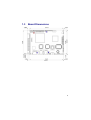
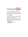
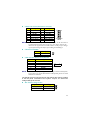
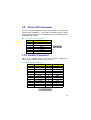
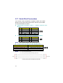
HS-2615 VIA V4 Eden processor Embedded Engine Board •CompactFlash•8-bit I/O•CRT/LVDS/DVI-I•TV-Out• •Dual LAN•Audio•SATA•ATA/33/66/100• •RS-232/422/485•4 COM•6 USB2.0• •PC/104•WDT•H/W Monitor• Copyright Disclaimers The accuracy of contents in this manual has passed through checking and review before publishing. BOSER Technology Co., Ltd., the manufacturer and publisher, is not liable for any infringements of patents or other rights resulting from its use. The manufacturer will not be responsible for any direct, indirect, special, incidental or consequential damages arising from the use of this product or documentation, even if advised of the possibility of such damage(s). This manual is copyrighted and BOSER Technology Co., Ltd. reserves all documentation rights. Unauthorized reproduction, transmission, translation, and storage of any form and means (i.e., electronic, mechanical, photocopying, recording) of this document, in whole or partly, is prohibited, unless granted permission by BOSER Technology Co., Ltd. BOSER Technology Co., Ltd. reserves the right to change or improve the contents of this document without due notice. BOSER Technology Co., Ltd. assumes no responsibility for any errors or omissions that may appear in this manual, nor does it make any commitment to update the information contained herein. TTrraaddeem maarrkkss BOSER is a registered trademark of BOSER Technology Co., Ltd. ISB is a registered trademark of BOSER Technology Co., Ltd. Intel is a registered trademark of Intel Corporation. Award is a registered trademark of Award Software, Inc. AMI is a registered trademark of AMI Software, Inc. All other trademarks, products and or product names mentioned herein are mentioned for identification purposes only, and may be trademarks and/or registered trademarks of their respective companies or owners. © Copyright 2008 BOSER Technology Co., Ltd. All Rights Reserved. Edition 2.1, January 28, 2011 Table of Contents Chapter 1 General Description ..................................1 1.1 Major Features ....................................................................... 2 1.2 Specifications ........................................................................ 3 1.3 Board Dimensions................................................................. 5 Chapter 2 Unpacking ..................................................5 2.1 Opening the Delivery Package............................................. 5 2.2 Inspection............................................................................... 5 Chapter 3 3.1 3.2 3.3 3.4 3.5 3.6 3.7 3.8 3.9 3.10 3.11 3.12 3.13 3.14 3.15 3.16 3.17 3.18 3.19 3.20 3.21 3.22 3.23 Hardware Installation ..............................7 Before Installation ................................................................. 7 Board Layout ......................................................................... 8 Jumper List ............................................................................ 9 Connector List ....................................................................... 9 Configuring the CPU ........................................................... 10 System Memory ................................................................... 10 VGA Controller .................................................................... 10 IDE Drive Connector ........................................................... 12 Serial ATA Connector ......................................................... 13 Parallel Connector............................................................... 13 Serial Port Connectors ....................................................... 14 Ethernet Connector............................................................. 15 USB Port............................................................................... 15 CMOS Data Clear................................................................. 16 Power and Fan Connectors................................................ 16 Keyboard/Mouse Connectors ............................................ 17 System Front Panel Control ............................................... 17 Watchdog Timer .................................................................. 18 TV-Out Function .................................................................. 21 PC/104 Connectors ............................................................. 21 Audio Connectors ............................................................... 24 CompactFlash Connector................................................ 24 8-bit I/O Function ................................................................. 26 Chapter 4 4.1 4.2 4.3 4.4 4.5 4.6 4.7 4.8 4.9 Chapter 5 5.1 5.2 5.3 5.4 5.5 5.6 5.7 5.8 5.9 5.10 5.11 Award BIOS Setup ................................. 45 Starting Setup...................................................................... 45 Using Setup ......................................................................... 46 Main Menu............................................................................ 47 Standard CMOS Features................................................... 48 Advanced BIOS Features ................................................... 49 Advanced Chipset Features............................................... 50 Integrated Peripherals ........................................................ 52 Power Management Setup ................................................. 54 PnP/PCI Configurations...................................................... 55 PC Health Status ................................................................. 56 Frequency/Voltage Control ................................................ 56 Chapter 6 6.1 6.2 6.3 6.4 AMI BIOS Setup ..................................... 29 Starting Setup...................................................................... 29 Using Setup ......................................................................... 30 Main Menu............................................................................ 31 Advanced Settings .............................................................. 32 Advanced PCI/PnP Settings............................................... 37 Boot Settings ....................................................................... 38 Security Settings ................................................................. 39 Advanced Chipset Settings................................................ 40 Exit Options ......................................................................... 43 Software Utilities..................................... 57 VGA Driver Installation ....................................................... 58 Audio Driver Installation..................................................... 59 LAN Driver Installation........................................................ 63 USB2.0 Driver Installation .................................................. 65 Declaration of Conformity -- CE Mark BOSER Technology hereby acknowledges that compliance testing in accordance with applicable standards of the EU’s EMC Directive, 89/336/EEC, was successfully completed on a sample of the equipment identified below: Equipment Class: Product Model Series: This Product Complies With: Information Technology Equipment HS-2615 EN55022: Class A for Radiated emissions EN50082-2: Heavy Industrial EMC Immunity We, the undersigned, hereby declare that the equipment specified above conforms to the above directives and standards. Manufacturer: BOSER TECHNOLOGY CO., LTD. Safety Instructions Integrated circuits on computer boards are sensitive to static electricity. To avoid damaging chips from electrostatic discharge, observe the following precautions: Do not remove boards or integrated circuits from their anti-static packaging until you are ready to install them. Before handling a board or integrated circuit, touch an unpainted portion of the system unit chassis for a few seconds. This helps to discharge any static electricity on your body. Wear a wrist-grounding strap, available from most electronic component stores, when handling boards and components. Fasten the ALLIGATOR clip of the strap to the end of the shielded wire lead from a grounded object. Please wear and connect the strap before handle the HS-2615 to ensure harmlessly discharge any static electricity through the strap. Please use an anti-static pad when putting down any components or parts or tools outside the computer. You may also use an anti-static bag instead of the pad. Please inquire from your local supplier for additional assistance in finding the necessary anti-static gadgets. NOTE: DO NOT TOUCH THE BOARD OR ANY OTHER SENSITIVE COMPONENTS WITHOUT ALL NECESSARY ANTI-STATIC PROTECTIONS. Chapter 1 General Description The HS-2615 is a VIA CX700(M) chipset-based board designed. The HS-2615 is an ideal all-in-one embedded engine board. Additional features include an enhanced I/O with CF, 8-bit I/O, CRT/LVDS, TV-Out, dual LAN, audio, SATA, 4 COM, 6 USB2.0, and PC/104 interfaces. Its onboard ATA/33/66/100 to IDE drive interface architecture allows the HS-2615 to support data transfers of 33 or 66MB/sec. to one IDE drive connection. Designed with the VIA CX700(M), the board supports VIA V4 Eden 1GHz CPU. The VIA CX700(M) with 32/64/128MB shared main memory supports CRT/Panel displays up to 1920 x 1440. It also supports 24-bit single/dual-channel LVDS interface supporting up to 1600 x 1200. System memory is also sufficient with the one SO-DDRII socket that can support up to 1G. Additional onboard connectors include 6 USB2.0 ports providing faster data transmission. And two RJ-45 connectors for 10/100 Based Ethernet uses. To ensure the reliability in an unmanned or standalone system, the watchdog timer (WDT) onboard HS-2615 is designed with software that does not need the arithmetical functions of a real-time clock chip. If any program causes unexpected halts to the system, the onboard WDT will automatically reset the CPU or generate an interrupt to resolve such condition. 1 1.1 Major Features The HS-2615 comes with the following features: ¾ ¾ ¾ ¾ ¾ ¾ ¾ 2 VIA V4 Eden processor 1GHz, supports 400MHz FSB 1 x SO-DIMM up to 1GB DDR2 SDRAM VIA CX700(M) system chipset VIA CX700(M) integrated VGA for CRT & LVDS 2 x 10/100 Mbps ethernet AC’97 audio codec Supports CF, 1 x SATA, 4 x COM, 6 x USB2.0, PC/104 ¾ ¾ 1.2 Supports 24-bit LVDS, TV-Out, 8-bit I/O, H/W Monitor function, Single +5V or +10~+30V wide range single DC power in Option for DVI-I display Specifications z System CPU: VIA V4 Eden processor 1.0GHz FSB: 400MHz FSB BIOS: Award PnP Flash BIOS System Chipset: VIA CX700(M) I/O Chipset: Winbond W83697UG System Memory: 1 x 200-pin SO-DIMM socket DDR2 533MHz up to 1GB Storage: 1 x Type II CF socket Watchdog Timer: Software programmable time-out intervals from 1~255 sec. or 1~255 min. H/W Status Monitor: Monitoring temperatures, voltages, and cooling fan status Expansion Interface: PC/104 Power In: +10~+30V wide range single DC power in (supports ATX power function) or single +5V power in (PCB ver:0.4 above) Operating Temperature: 0~60 degrees C Operating Humidity: 0~95%, non-condensing Size (L x W): 145 x 102 mm 3 z I/O Interface MIO: 3 x RS-232 1 x RS-232/422/485 6 x USB2.0 (4 x internal, 2 x external) 1 x IDE 1 x Parallel 1 x SATA 1 x PS/2 for KB/MS DI/O: 8-bit input/output z Display Chipset: VIA CX700(M) Display Memory: 32/64/128MB video memory LVDS: 24-bit single/dual-channel TV-Out: Provides PAL or NTSC TV systems DVI Chipset: VIA CX700(M) (option) Resolution: CRT Mode: 1920 x 1440 LVDS Mode: 1600 x 1200 z Audio Chipset: VIA VT1708A Audio Interface (w/pin header): MIC In, Line Out z Ethernet 4 Chipset: Dual RealTek RTL8139DL 10/100 Mbps LAN Ethernet Interface: 2 x RJ-45 1.3 Board Dimensions 5 This page is the blank page. 6 Chapter 2 Unpacking 2.1 Opening the Delivery Package The HS-2615 is packed in an anti-static bag. The board has components that are easily damaged by static electricity. Do not remove the anti-static wrapping until proper precautions have been taken. Safety Instructions in front of this manual describe anti-static precautions and procedures. 2.2 Inspection After unpacking the board, place it on a raised surface and carefully inspect the board for any damage that might have occurred during shipment. Ground the board and exercise extreme care to prevent damage to the board from static electricity. Integrated circuits will sometimes come out of their sockets during shipment. Examine all integrated circuits, particularly the BIOS, processor, memory modules, ROM-Disk, and keyboard controller chip to ensure that they are firmly seated. The HS-2615 delivery package contains the following items: HS-2615 Board x 1 Utility CD Disk x 1 including User’s Manual Cables (as following table) Jumper Bag x 1 5 Cables Package Description NO. 1 2 3 4 5 6 7 SPK 8-pin(2.0-pitch) phone jack x 2 4-pin to 4-pin terminal block power cable (for +12V version only) COM DB9-10P (2.0-pitch) 1-to-2 Mini DIN cable DB25-26P Printer cable 2-pin to 4-pin power cable (for +5V version only) SATA device cable QTY. 1 1 2 1 1 1 1 It is recommended that you keep all the parts of the delivery package intact and store them in a safe/dry place for any unforeseen event requiring the return shipment of the product. In case you discover any missing and/or damaged items from the list of items, please contact your dealer immediately. Option Accessories NO. Description 1 2 3 4 6 SATA power cable 1-to-2 USB cable with bracket COM DB9-10P (2.0-pitch) 40-pin to 44-pin IDE flat cable Chapter 3 Hardware Installation This chapter provides the information on how to install the hardware using the HS-2615. This chapter also contains information related to jumper settings of switch, and watchdog timer selection etc. 3.1 Before Installation After confirming your package contents, you are now ready to install your hardware. The following are important reminders and steps to take before you begin with your installation process. 1. Make sure that all jumper settings match their default settings and CMOS setup correctly. Refer to the sections on this chapter for the default settings of each jumper. (JP3 short 1-2) 2. Go through the connections of all external devices and make sure that they are installed properly and configured correctly within the CMOS setup. Refer to the sections on this chapter for the detailed information on the connectors. 3. Keep the manual and diskette in good condition for future reference and use. 7 3.2 8 Board Layout 3.3 Jumper List Jumper JP1 JP3 JP5 JP6 CN23 3.4 Default Setting Panel Voltage Select: +3.3V Clear CMOS: Normal Operation CF Use Master/Slave Select: Slave Display Out Function Select: CRT COM4 Use RS-232 or RS-422/485 Select: RS-232 Setting Page Short 1-2 Short 1-2 Short 2-3 Short 1-2 10 16 23 20 Open 14 Connector List Connector CN1/CN2 CN3 CN4/CN5/CN7 CN6 CN8 CN9/CN12 CN10 CN11/CN13 CN14 CN15 CN16 CN17 CN24/CN18/CN19/CN25 CN20 CN21 CN22 CN26 CN27 CN28 CN29 CN30 CN31 CN32 FN1 Definition PC/104 Bus 40-pin/64-pin Connector Reset Button USB2.0 Port Serial ATA Connector Inverter Power In Connector LVDS Panel Connector IDE Connector RJ-45 Connector Parallel Port PS/2 6-pin Mini DIN 4-pin Power In Connector 15-pin CRT Connector COM 1~COM 4 Connector (5x2 header) 2-pin ATX Power In Connector System Front Panel Control MIC In/Line Out Connector RS-422/485 Connector SO-DDRII Socket CompactFlash Connector TV-Out Connector 8-bit Input/Output 2-pin Power In Connector DVI SM Bus Fan Power In Connector Page 20 16 15 12 10 10 12 15 13 17 16 10 14 16 17 23 14 10 23 20 25 16 10 16 9 3.5 Configuring the CPU The HS-2615 embedded with VIA V4 Eden processor 1.0GHz. User don’t need to adjust the frequently and check speed of CPU. 3.6 System Memory The HS-2615 provides one SO-DDRII socket at locations CN27. The maximum capacity of the onboard memory is 1GB. 3.7 VGA Controller The HS-2615 provides two connection methods of a VGA device. CN17 offers an internal 15-pin CRT connector and CN9/CN12 are the LVDS interface connectors onboard reserved for flat panel installation. HS-2615 also provides DVI function. There is an optional cable for this function use (CN9 + CN32). z CN17: 15-pin CRT Connector PIN Description PIN Description 1 3 5 7 9 11 13 15 10 Red Blue GND GND N/C N/C HSYNC SDC 2 4 6 8 10 12 14 Green N/C GND GND GND SDA VSYNC 1 6 11 5 10 15 z CN9/CN12: LVDS Interface Connector PIN Description PIN Description 1 3 5 7 9 11 13 NOTE: VLCD GND A0-/B0A1-/B1A2-/B2CLK1-/CLK2A3-/B3- 2 4 6 8 10 12 14 VLCD GND A0+/B0+ A1+/B1+ A2+/B2+ CLK1+/CLK2+ A3+/B3+ 1 2 13 14 LVDS cable should be produced very carefully. A0- & A0+ have to be fabricated in twister pair (A1- & A1+, A2- & A2+ and so on) otherwise the signal won’t be stable. Please set the proper voltage of your panel using JP1 before proceeding on installing it. z CN32: DVI SM Bus PIN Description 1 2 SPD1 SPCLK1 1 2 z CN8: Inverter Power In Connector NOTE: PIN Description 1 2 3 4 5 6 N/C N/C VCC BK_EN ENVDD GND 1 6 If use CN9 only, it just supports 24-bit single channel LVDS panel; If you want to use 48-bit dual channel LVDS panel, please use CN9 and CN12 combined. The HS-2615 has an onboard jumper that selects the working voltage of the flat panel connected to the system. Jumper JP1 offers two voltage settings for the user. z JP1: Panel Voltage Select Options Settings 1 +3.3V (default) +5V Short 1-2 Short 2-3 3 11 3.8 IDE Drive Connector CN10 is a 2.0-pitch 44-pin connector which support 2 ATA/33/66/100 IDE drives can be connected to the HS-2615 via CN10. z CN10: IDE Connector PIN Description PIN Description 1 3 5 7 9 11 13 15 17 19 21 23 25 27 29 31 33 35 37 39 41 43 Reset PDD7 PDD6 PDD5 PDD4 PDD3 PDD2 PDD1 PDD0 GND PDREQ IOW# IOR# PIORDY RPDACKInterrupt RPDA1RPDA0RPCS1HDD Active VCC GND 2 4 6 8 10 12 14 16 18 20 22 24 26 28 30 32 34 36 38 40 42 44 GND PDD8 PDD9 PDD10 PDD11 PDD12 PDD13 PDD14 PDD15 N/C GND GND GND PR1PD1GND N/C PATA66 RPDA2RPCS3GND VCC N/C 43 44 12 1 2 3.9 Serial ATA Connector You can connect the Serial ATA device that provides you high speeds transfer rates (150MB/sec.). If you wish to use RAID function, please note that these two serial ATA connectors just support RAID0 and only compatible with WIN XP. z CN6: Serial ATA Connector PIN Description 1 2 3 4 5 6 7 GND SATATXP SATATXN GND SATARXN SATARXP GND 1 7 3.10 Parallel Connector CN14 is a standard 26-pin flat cable connector designed to accommodate onboard parallel port connection. z CN14: Parallel Connector PIN Description PIN Description 1 2 3 4 5 6 7 8 9 10 11 12 13 Strobe DATA0 DATA1 DATA2 DATA3 DATA4 DATA5 DATA6 DATA7 Acknowledge Busy Paper Empty Printer Select 14 15 16 17 18 19 20 21 22 23 24 25 26 Auto From Feed ERROR# Initialize Printer Select LN# GND GND GND GND GND GND GND GND GND 13 1 26 14 13 3.11 Serial Port Connectors The HS-2615 offers NS16C550 compatible UARTs with Read/ Receive 16-byte FIFO serial ports and four internal 10-pin headers and one RS-422/485 connector. z CN24/CN18/CN19/CN25: COM 1 ~ COM 4 Connector (5x2 Header) PIN Description PIN Description 1 3 5 7 9 z DCD RXD TXD DTR GND 2 4 6 8 10 DSR RTS CTS RI N/C 9 1 10 2 CN26: RS-422/485 Connector (3x2 Header, COM 4) PIN Description PIN Description 1 3 5 NOTE: z TXRX+ GND 2 4 6 TX+ RXN/C 5 1 6 2 The terminal resistance of RX & TX is set at 180Ω. CN23: COM 4 use RS-232 or RS-422/485 Select Options Settings RS-232 (default) RS-485 by Transmit Only (*1) RS-485 by –RTS (*-1) RS-422/485 Full Duplex (*2) Open Short 1-2, 3-4, 5-7, 8-10 Short 1-2, 3-4, 7-9, 8-10 Short 1-2, 3-4, 6-8 NOTE: *1: 2-wires RS-485 function *2: 4-wires point-to-point full duplex function 4-wires point-to-point full duplex RS-422/485 14 9 1 10 2 Typical RS-485 2-wires Mutildrop Network 3.12 Ethernet Connector The HS-2615 provides two RJ-45 connectors for 10/100 Based LAN. Please refer to the following for its pin information. When installs OS, this driver namely can automatically install. User does not need to renewal. z CN11/CN13: RJ-45 Connector PIN Description PIN Description 1 2 3 4 5 6 7 8 9 TCT TXRXN/C N/C Link LED ACT LED SHIELD SHIELD 10 11 12 13 14 15 16 17 18 TX+ RX+ N/C N/C RCT 330Ω pull VCC3 330Ω pull VCC3 SHIELD SHIELD 1 8 3.13 USB Port The HS-2615 provides three connectors, at location CN4/CN5/CN7, for six USB2.0 ports. z CN4/CN5: Internal USB2.0 Connector PIN Description PIN Description 1 3 5 7 VCC USBD0-/USBD2USBD0+/USBD2+ GND 2 4 6 8 VCC USBD1-/USBD3USBD1+/USBD3+ GND 1 2 7 8 15 z CN7: External USB2.0 Port PIN Description PIN Description 1 3 5 7 VCC USBD4USBD4+ GND 2 4 6 8 VCC USBD5USBD5+ GND 3.14 CMOS Data Clear The HS-2615 has a Clear CMOS jumper on JP3. z JP3: Clear CMOS Options Settings 1 Normal Operation (default) Clear CMOS Short 1-2 Short 2-3 3 IMPORTANT: Before turn on the power of system, please set JP3 to Short 1-2 for normal operation. 3.15 Power and Fan Connectors HS-2615 provides one 4-pin power in at CN16. Connector FN1 onboard HS-2615 is a 3-pin fan power connector. z CN20: 2-pin ATX Power In Connector PIN Description 1 2 PS_ON 5VSB 2 1 z FN1: Fan Power In Connector PIN Description 1 2 3 GND VCC Fan In 1 3 z CN3: External Reset Button 16 PIN Description 1 2 3 4 GND Reset Switch GND GND 3 1 4 2 z CN16: 4-pin Power In Connector PIN Description 1 2 3 4 DC In GND GND DC In 1 4 z CN31: 2-pin Power In Connector PIN Description 1 2 VCC GND 2 1 3.16 Keyboard/Mouse Connectors The CN15 is a PS/2 6-pin Mini DIN connector for HS-2615. z CN15: PS/2 6-pin Mini DIN Keyboard/Mouse Connector PIN Description 1 2 3 4 5 6 Keyboard Data Mouse Data GND +5V Keyboard Clock Mouse Clock 6 4 2 5 3 1 3.17 System Front Panel Control The HS-2615 has front panel control at location CN21 that indicates the power-on status. z CN21: System Front Panel Control PIN Description 1 3 5 7 9 11 330Ω pull VCC HDD LED PWR Button GND Reset Switch GND PIN Description 2 4 6 8 10 12 Speaker N/C GND 330Ω pull VCC 330Ω pull 3.3V GND 17 Connector CN21 Orientation HDD LED PWR Button Reset Button 1 2 3 4 5 6 7 8 9 10 11 12 Speaker PWR LED 3.18 Watchdog Timer A user can set a value of Watchdog Timer in his software to reboot their hardware system. It is forced to reboot once user’s software fails to reset the Watchdog Timer before the counter of Watchdog Timer meets user’s setting value. This function, Watchdog Timer, prevents user’s software from crashing. W83697UF Watch Dog Timer 1. Assembly sample code: -----------------------------------Extended function mode -----------------------------------MOV DX,4EH MOV AL,87H OUT DX,AL OUT DX,AL ------------------------------------Configure logical device 8 ------------------------------------MOV DX,4EH MOV AL,07H OUT DX,AL MOV DX,4FH MOV AL,08H OUT DX,AL 18 MOV DX,4EH ; Define WDT MOV AL,2BH OUT DX,AL MOV DX,4FH MOV AL,00H OUT DX,AL MOV DX,4EH MOV AL,30H ; Enable WDT OUT DX,AL MOV DX,4FH MOV AL,01H OUT DX,AL -------------------------------------Configure time mode -------------------------------------MOV DX,4EH MOV AL,F3H OUT DX,AL MOV DX,4FH MOV AL,00H ; Setup second mode, 08H for minute mode OUT DX,AL --------------------------------------Configure reset time interval --------------------------------------MOV DX,4EH MOV AL,F4H OUT DX,AL MOV DX,4FH MOV AL,05H ; Setup reset time 5, User can setup from 1~255 OUT DX,AL 19 2. DOS Debug Command -----------------------------o 4e,87 o 4e,87 o 4e,07 o 4f,08 o 4e,30 o 4f,01 o 4e,f3 o 4f,00 o 4e,f4 o 4f,05 20 3.19 TV-Out Function The HS-2615 can support TV-out function whose input could be up to 800 x 600 graphics resolutions. World Wide Video standards are supported including NTSC-M (North America, Taiwan), NTSC-J (Japan), PAL-b, D, G, H, I (Europe, Asia), PAL-M (Brazil), PAL-N (Uruguay, Paraguay) and PAL-NC (Argentina). z CN29: TV-Out Connector PIN Description 1 2 CVBS GND 1 2 z JP6: Display Out Function Select Options Settings 1 TV-Out CRT (default) Short 2-3 Short 1-2 3 3.20 PC/104 Connectors The PC/104 expansion bus offers provisions to connect all types of PC/104 modules. With the PC/104 bus being known as the new generation of industrial embedded 16-bit PC standard bus, thousands of PC/104 modules from multiple venders can be easily installed onboard. The detailed pin assignment of the PC/104 expansion bus connectors CN2 and CN1 are listed on the following tables: NOTE1: The PC/104 connector allows direct plugging or stack-through piling of PC/104 modules without requiring the PC/104 mounting kit. NOTE2: PC/104 Bus connector only for 16-bit ISA Bus, DO NOT support DMA mode. NOTE3: There is a special fanless heatsink for HS-2615 to integrate the PC/104 module, need more information, please contact with your sales. 21 z CN1: PC/104 40-pin Connector PIN 1 2 3 4 5 6 7 8 9 10 11 12 13 14 15 16 17 18 19 20 22 Description PIN Description GND -MEMCS16 -IOSC16 IRQ10 IRQ11 IRQ12 IRQ15 IRQ14 -DACK0 DRQ0 -DACK5 DRQ5 -DACK6 DRQ6 -DACK7 DRQ7 +5V -MASTER GND GND 21 22 23 24 25 26 27 28 29 30 31 32 33 34 35 36 37 38 39 40 GND -SBHE SA23 SA22 SA21 SA20 SA19 SA18 SA17 -MEMR -MEMW SD8 SD9 SD10 SD11 SD12 SD13 SD14 SD15 N/C Connector diagram rotated 90 degrees clockwise from original position 1 21 20 40 z CN2: PC/104 64-pin Connector PIN 1 2 3 4 5 6 7 8 9 10 11 12 13 14 15 16 17 18 19 20 21 22 23 24 25 26 27 28 29 30 31 32 Description PIN Description -IOCHECK SD7 SD6 SD5 SD4 SD3 SD2 SD1 SD0 IOCHRDY AEN SA19 SA18 SA17 SA16 SA15 SA14 SA13 SA12 SA11 SA10 SA9 SA8 SA7 SA6 SA5 SA4 SA3 SA2 SA1 SA0 GND 33 34 35 36 37 38 39 40 41 42 43 44 45 46 47 48 49 50 51 52 53 54 55 56 57 58 59 60 61 62 63 64 GND RESETDRV +5V IRQ9 N/C DRQ2 -12V N/C +12V GND -SMEMW -SMEMR -IOW -IOR -DACK3 DRQ3 -DACK1 DRQ1 -REFRESH SYSCLK IRQ7 IRQ6 IRQ5 IRQ4 IRQ3 -DACK2 TC BALE +5V OSC N/C GND Connector diagram rotated 90 degrees clockwise from original position 1 33 32 64 23 3.21 Audio Connectors The HS-2615 has an onboard VIA VT1708A High Definition Audio CODEC. The following tables list the pin assignments of the Line In/Audio Out connector. 4 stereo DACs support 24-bit, 192KHz samples DAC with 100dB S/N Ratio 2 stereo ADCs support 24-bit, 192KHz samples ADC with 95dB S/N ratio 8-channels of DAC support 16/20/24-bit PCM format for 7.1 audio solution z CN22: MIC In/Line Out Connector PIN Description PIN Description 1 3 5 7 AOUTL GND MIC IN L GND 2 4 6 8 AOUTR GND LINE R LINE L 1 2 7 8 3.22 CompactFlash Connector The HS-2615 also offers a Type I/II CompactFlash connector is IDE interface located at the solder side of the board. The designated CN28 connector, once soldered with an adapter, can hold CompactFlash cards of various sizes. Please turn off the power before inserting the CF card. Inserting a CompactFlash card into the adapter is not a difficult task. The socket and card are both keyed and there is only one direction for the card to be completely inserted. Refer to the diagram on the following page for the traditional way of inserting the card. z JP5: CF Use Master/Slave Select 24 Options Setting 1 Master Slave (default) Short 1-2 Short 2-3 3 z CN28: CompactFlash Connector PIN Description PIN Description 1 3 5 7 9 11 13 15 17 19 21 23 25 27 29 31 33 35 37 39 41 43 45 47 49 GND DATA4 DATA6 SDCS1# GND GND VCC GND GND SDA1 DATA0 DATA2 N/C DATA11 DATA13 DATA15 N/C IOW IRQ CS RESET DACK IDE LED DATA8 DATA10 2 4 6 8 10 12 14 16 18 20 22 24 26 28 30 32 34 36 38 40 42 44 46 48 50 DATA3 DATA5 DATA7 GND GND GND GND GND SDA2 SDA0 DATA1 470Ω pull GND N/C DATA12 DATA14 SDCS3# UOR EWE0 VCC N/C IORDY REQ PDIAG DATA9 GND NOTE: When use CF card, IDE device function will be disabled. 25 3.23 8-bit I/O Function The HS-2615 offers one 8-bit input/output port by parallel port. z CN30: 8-bit Input/Output PIN Description PIN Description 1 3 5 7 9 VCC GD0 GD1 GD2 GD3 2 4 6 8 10 GND GD4 GD5 GD6 GD7 W83697 Digital I/O Assembly sample code -----------------------------------Extended function mode -----------------------------------MOV DX,4EH MOV AL,87H OUT DX,AL OUT DX,AL ------------------------------------Configure logical device 7 ------------------------------------MOV DX,4EH MOV AL,07H OUT DX,AL MOV DX,4FH MOV AL,07H OUT DX,AL MOV DX,4EH MOV AL,30H OUT DX,AL MOV DX,4FH MOV AL,01H 26 ; Enable GPIO1 9 1 10 2 OUT DX,AL --------------------------------------Configure input / output --------------------------------------MOV DX,4EH MOV AL,F0H OUT DX,AL MOV DX,4FH MOV AL,FEH ; Setup GPIO bit0 as output, 0: output 1: input OUT DX,AL 27 This page is the blank page. 28 Chapter 4 AMI BIOS Setup The HS-2615 uses AMI BIOS for the system configuration. The AMI BIOS setup program is designed to provide the maximum flexibility in configuring the system by offering various options that could be selected for end-user requirements. This chapter is written to assist you in the proper usage of these features. 4.1 Starting Setup The AMI BIOS is immediately activated when you first power on the computer. The BIOS reads the system information contained in the CMOS and begins the process of checking out the system and configuring it. When it finishes, the BIOS will seek an operating system on one of the disks and then launch and turn control over to the operating system. While the BIOS is in control, the Setup program can be activated in one of two ways: 1. By pressing <Del> immediately after switching the system on, or 2. By pressing the <Del> key when the following message appears briefly at the bottom of the screen during the POST (Power On Self Test). Press DEL to enter SETUP. If the message disappears before you respond and you still wish to enter Setup, restart the system to try again by turning it OFF then ON or pressing the "RESET" button on the system case. You may also restart by simultaneously pressing <Ctrl>, <Alt>, and <Delete> keys. If you do not press the keys at the correct time and the system does not boot, an error message will be displayed and you will be asked to... PRESS F1 TO CONTINUE, DEL TO ENTER SETUP 29 4.2 Using Setup In general, you use the arrow keys to highlight items, press <Enter> to select, use the <PageUp> and <PageDown> keys to change entries, and press <Esc> to quit. The following table provides more detail about how to navigate in the Setup program using the keyboard. ↑ ↓ ← → Esc key PgUp key PgDn key + key - key F1 key F2 key F3 key F4 key F5 key F6 key F7 key F8 key F9 key F10 key 30 Move to previous item Move to next item Move to previous item Move to previous item Main Menu -- Quit and not save changes into CMOS Status Page Setup Menu and Option Page Setup Menu -Exit current page and return to Main Menu Decrease the numeric value or make changes Increase the numeric value or make changes Increase the numeric value or make changes Decrease the numeric value or make changes Reserved Change color from total 8 colors. F2 to select color forward F2 to select color backward Reserved Reserved Reserved Reserved Reserved Reserved Save all the CMOS changes, only for Main Menu 4.3 Main Menu Once you enter the AMI BIOS CMOS Setup Utility, the Main Menu will appear on the screen. The Main Menu allows you to select from several setup functions and two exit choices. Use the arrow keys to select among the items and press <Enter> to enter the sub-menu. BIOS SETUP UTILITY Main Advanced System Overview PCIPnP Boot Security Chipset Exit AMI BIOS Version : 08.00.14 Build Date : 10/18/07 ID : HS261500 Processor Type : VIA Esther processor 1000MHz Speed : 1000MHz Count : 1 System Memory Size : 448MB Select Screen Select Item System Time [00:29:32] +Change Field System Date [Tue 01/01/2002] Tab Select Field F1 General Help F10 Save and Exit ESC Exit v02.59 (C)Copyright 1985-2005, American Megatrends, Inc. NOTE: ← ↑↓ A brief description of the highlighted choice appears at the bottom of the screen. 31 4.4 Advanced Settings This section allows you to configure your system for the basic operation. You have the opportunity to select the system’s default speed, boot-up sequence, keyboard operation, shadowing and security. BIOS SETUP UTILITY Main Advanced Advanced Settings PCIPnP Boot Security Chipset Exit WARNING: Setting wrong values in below sections may cause system to malfunction. CPU Configuration IDE Configuration Floppy Configuration SuperIO Configuration ACPI Configuration APM Configuration Hardware Health Configuration MPS Configuration PCI Express Configuration Smbios Configuration USB Configuration Select Screen Select Item ª - Change Field Tab Select Field F1 General Help F10 Save and Exit ESC Exit v02.59 (C)Copyright 1985-2005, American Megatrends, Inc. BIOS SETUP UTILITY Main Advanced PCIPnP Configure advanced CPU settings Module Version:3F.01 Manufacturer : Boot Security Chipset Exit VIA VIA Esther processor 1000MHz Frequency : 1.00GHz FSB Speed : 400MHz Cache L1 : 128 KB Cache L2 : 128 KB Select Screen Ratio Actual Value : 10 Select Item ª CMPXCHG8B instruction support [Enabled] VIA Processor Power Management [Enabled] - Change Field Tab Select Field F1 General Help F10 Save and Exit ESC Exit v02.59 (C)Copyright 1985-2005, American Megatrends, Inc. 32 BIOS SETUP UTILITY Main Advanced IDE Configuration PCIPnP Boot Parallel ATA IDE device Primary IDE Master Primary IDE Slave Secondary IDE Master Secondary IDE Slave : : : : Parallel ATA IDE Controller Hard Disk Write Protect IDE Detect Time Out (Sec) ATA(PI) 80Pin Cable Detection [Both] [Disabled] [35] [Host] [Not [Not [Not [Not Security Chipset Exit Detected] Detected] Detected] Detected] Select Screen Select Item ª - Change Field Tab Select Field F1 General Help F10 Save and Exit ESC Exit v02.59 (C)Copyright 1985-2005, American Megatrends, Inc. BIOS SETUP UTILITY Main Advanced PCIPnP Boot Configure WIN697UF Super IO Chipset OnBoard Floppy Controller Floppy Drive Swap Serial Port1 Address Serial Port2 Address Serial Port3 Address Serial Port3 IRQ Select Serial Port4 Address Serial Port4 IRQ Select Parallel Port Address Parallel Port Mode Parallel Port IRQ Security Chipset Exit [Disabled] [Disabled] [3F8/IRQ4] [2F8/IRQ3] [3E8] [IRQ11] [2E8] [IRQ10] [378] [Normal] [IRQ7] Select Screen Select Item ª Change Field Tab Select Field F1 General Help F10 Save and Exit ESC Exit v02.59 (C)Copyright 1985-2005, American Megatrends, Inc. 33 BIOS SETUP UTILITY Main Advanced ACPI Settings ACPI Aware O/S PCIPnP Boot Security Chipset Exit [No] Select Screen Select Item ª Change Field Tab Select Field F1 General Help F10 Save and Exit ESC Exit v02.59 (C)Copyright 1985-2005, American Megatrends, Inc. 34 BIOS SETUP UTILITY Main Advanced PCIPnP Boot Security Power Management/APM [Enabled] Power Button Mode Suspend Power Saving Type Restore on AC/Power Loss Manual Throttle Ratio System Thermal Thermal Active Temperature THRM throttle Ratio [On/Off] [C3] [Last State] [50%-56.25%] [Disabled] [65°C/149°F] [50%-56.25%] Standby Time Out Suspend Time Out Hard Disk Time Out (Minute) [Disabled] [Disabled] [Disabled] Green PC Monitor Power State Video Power Down Mode Hard Disk Power Down Mode [Suspend] [Suspend] [Suspend] Advanced Monitor Events Controls Display Activity Monitor IRQ3 Monitor IRQ4 Monitor IRQ5 Monitor IRQ7 Monitor IRQ9 Monitor IRQ10 Monitor IRQ11 Monitor IRQ13 Monitor IRQ14 Monitor IRQ15 [Ignore] [Monitor] [Ignore] [Ignore] [Ignore] [Ignore] [Ignore] [Ignore] [Ignore] [Monitor] [Ignore] Chipset Exit Advanced Resume Events Controls Select Screen Resume On Ring [Disabled] Select Item Resume On PME# [Disabled] ª Change Field Resume On KBC [Disabled] Tab Select Field Wake-Up Key [Any Key] F1 General Help Resume On PS/2 Mouse [Disabled] F10 Save and Exit Resume On RTC Alarm [Disabled] ESC Exit v02.59 (C)Copyright 1985-2005, American Megatrends, Inc. 35 BIOS SETUP UTILITY Main Advanced PCIPnP Boot Security H/W Health Function [Enabled] CPU Temperature System Temperature : : Fan 1 Reading : : Vcore(VIN1) +3.3V(VIN2) VBAT(VIN3) VCC : : : : Chipset Exit Select Screen Select Item ª Change Field Tab Select Field F1 General Help F10 Save and Exit ESC Exit v02.59 (C)Copyright 1985-2005, American Megatrends, Inc. BIOS SETUP UTILITY Main Advanced USB Configuration PCIPnP Boot Security Chipset Exit Module Version – 2.24.0-11.4 USB Devices Enabled: None USB 1.1 Ports Configuration USB 2.0 Ports Enable Legacy USB Support Port 64/60 Emulation USB 2.0 Controller Mode BIOS EHCI Hand-Off [USB 6 Ports] [Enabled] [Enabled] [Disabled] [HiSpeed] [Enabled] Select Screen Select Item ª Change Field Tab Select Field F1 General Help F10 Save and Exit ESC Exit v02.59 (C)Copyright 1985-2005, American Megatrends, Inc. 36 4.5 Advanced PCI/PnP Settings This section describes configuring the PCI bus system. PCI, or Personal Computer Interconnect, is a system that allows I/O devices to operate at speeds nearing the speed the CPU itself uses when communicating with its own special components. This section covers some very technical items and it is strongly recommended that only experienced users should make any changes to the default settings. BIOS SETUP UTILITY Main Advanced PCIPnP Advanced PCI/PnP Settings Boot Security Chipset Exit WARNING: Setting wrong values in below sections may cause system to malfunction. Clean NVRAM [No] Plug & Play O/S [No] PCI Latency Timer [64] Allocate IRQ to PCI VGA [Yes] Palette Snooping [Disabled] PCI IDE BusMaster [Disabled] Offboard PCI/ISA IDE Card [Auto] IRQ3 IRQ4 IRQ5 IRQ7 IRQ9 IRQ10 IRQ11 IRQ14 IRQ15 DMA DMA DMA DMA DMA DMA Channel Channel Channel Channel Channel Channel [Available] [Available] [Available] [Available] [Available] [Available] [Available] [Available] [Available] 0 1 3 5 6 7 [Available] [Available] [Available] [Available] [Available] [Available] Select Screen Select Item ª Change Field Tab Select Field F1 General Help F10 Save and Exit Reserved Memory Size [Disabled] ESC Exit v02.59 (C)Copyright 1985-2005, American Megatrends, Inc. 37 4.6 Boot Settings BIOS SETUP UTILITY Main Advanced Boot Settings PCIPnP Boot Security Chipset Exit Boot Settings Configuration Select Screen Select Item ª Change Field Tab Select Field F1 General Help F10 Save and Exit ESC Exit v02.59 (C)Copyright 1985-2005, American Megatrends, Inc. BIOS SETUP UTILITY Main Advanced PCIPnP Boot Settings Configuration Quick Boot Quiet Boot AddOn ROM Display Mode Bootup Nom-Lock PS/2 Mouse Support Wait For ‘F1’ If Error Hit ‘DEL’ Message Display Interrupt 19 Capture Boot Security [Enabled] [Disabled] [Force BIOS] [On] [Auto] [Enabled] [Enabled] [Disabled] Chipset Exit Select Screen Select Item ª Change Field Tab Select Field F1 General Help F10 Save and Exit ESC Exit v02.59 (C)Copyright 1985-2005, American Megatrends, Inc. 38 4.7 Security Settings BIOS SETUP UTILITY Main Advanced Security Settings PCIPnP Supervisor Password User Password Boot Security Chipset Exit : Not Installed : Not Installed Select Screen Select Item ª Change Field [Disabled] Tab Select Field F1 General Help F10 Save and Exit ESC Exit v02.59 (C)Copyright 1985-2005, American Megatrends, Inc. Change Supervisor Password Change User Password Boot Sector Virus Protection 39 4.8 Advanced Chipset Settings BIOS SETUP UTILITY Main Advanced PCIPnP Advanced Chipset Settings WARNING: Setting wrong sections may malfunction. Boot Security Chipset Exit values in below cause system to NorthBridge VIA CX700 Configuration SouthBridge VIA CX700 Configuration Select Screen Select Item ª Change Field Tab Select Field F1 General Help F10 Save and Exit ESC Exit v02.59 (C)Copyright 1985-2005, American Megatrends, Inc. BIOS SETUP UTILITY Main Advanced PCIPnP Boot NorthBridge VIA CX700 Configuration Security DRAM Clock/Timing Configuration AGP & P2P Bridge Configuration V-Link & PCI Bus Configuration OnChip VGA Configuration Top Performance [Disabled] Software Reset E2 issue [Escape Patch] Change DCLK using RDCKM [Program] Chipset Exit Select Screen Select Item ª Change Field Tab Select Field F1 General Help F10 Save and Exit ESC Exit v02.59 (C)Copyright 1985-2005, American Megatrends, Inc. 40 BIOS SETUP UTILITY Main Advanced PCIPnP Boot DRAM Frequency/Timing Configuration DRAM Frequency DRAM Timing DRAM Command Rate RDSAIT/RDSBIT mode Memory Chip Driving DDR2 Memory Chip ODT DDR DQSBAR BA0 SEL BA1 SEL BA2 SEL BA Scramble DQSO scanning mode Security Chipset Exit [Auto] [Auto] [2T Command] [Auto] [Normal] [Auto] [Disabled] [A13] [A14] [A15] [Disabled] [Disabled] Select Screen Select Item ª - Change Field Tab Select Field F1 General Help F10 Save and Exit ESC Exit v02.59 (C)Copyright 1985-2005, American Megatrends, Inc. BIOS SETUP UTILITY Main Advanced PCIPnP AGP & P2P Bridge Configuration Boot Security Primary Graphics Adapter [PCI] AGP AGP AGP AGP AGP AGP [128MB] [8X] [Auto] [Enabled] [Disabled] [Disabled] Aperture Size 3.0 Mode Driving Control Fast Write Master 1 WS Read Master 1 WS Write AGP 3.0 Calibration cycle Chipset Exit [Disabled] Select Screen Select Item ª - Change Field Tab Select Field F1 General Help F10 Save and Exit ESC Exit v02.59 (C)Copyright 1985-2005, American Megatrends, Inc. 41 BIOS SETUP UTILITY Main Advanced PCIPnP V-Link & PCI Bus Configuration PCI Master 0 WS Write V-Link mode selection V-Link 8X Supported V-Link Data 2X Support DRDY Timing RCONV Dynamic CKE select Dynamic Clock Stop Control PCI Read Caching Select Boot Security Chipset Exit [Enabled] [Auto] [Enabled] [Disabled] [Default] [Enabled] [Auto] [FB] [EE] Select Screen Select Item ª - Change Field Tab Select Field F1 General Help F10 Save and Exit ESC Exit v02.59 (C)Copyright 1985-2005, American Megatrends, Inc. OnChip VGA Configuration Main Advanced PCIPnP VGA Frame Buffer Size CPU Direct Access Frame Buffer Select Display Device Panel Type Outport port Dithering TV H/W Layout TV Type TV Output Connector Boot Security [64MB] [Enabled] [CRT] [01] [DI0] [Disabled] [Default] [NTSC] [CVBS (Composite)] Chipset Exit Select Screen Select Item ª - Change Field Tab Select Field F1 General Help F10 Save and Exit ESC Exit v02.59 (C)Copyright 1985-2005, American Megatrends, Inc. SouthBridge VIA CX700 Configuration Main Advanced PCIPnP * Serial ATA IDE Controller * High Definition Audio Boot [IDE] [Auto] Security Chipset Exit Select Screen Select Item PCI Delay Transaction [Disabled] ª - Change Field Tab Select Field F1 General Help F10 Save and Exit ESC Exit v02.59 (C)Copyright 1985-2005, American Megatrends, Inc. 42 4.9 Exit Options BIOS SETUP UTILITY Main Advanced Exit Options PCIPnP Boot Security Chipset Exit Save Changes and Exit Discard Changes and Exit Discard Changes Load Optimal Defaults Load Failsafe Defaults Select Screen Select Item ª - Change Field Tab Select Field F1 General Help F10 Save and Exit ESC Exit v02.59 (C)Copyright 1985-2005, American Megatrends, Inc. 43 This page is the blank page. 44 Chapter 5 AWARD BIOS Setup The HS-7280 uses AWARD BIOS for the system configuration. The AWARD BIOS setup program is designed to provide the maximum flexibility in configuring the system by offering various options that could be selected for end-user requirements. This chapter is written to assist you in the proper usage of these features. 5.1 Starting Setup The AWARD BIOS is immediately activated when you first power on the computer. The BIOS reads the system information contained in the CMOS and begins the process of checking out the system and configuring it. When it finishes, the BIOS will seek an operating system on one of the disks and then launch and turn control over to the operating system. While the BIOS is in control, the Setup program can be activated by pressing the <Del> key when the following message appears briefly at the bottom of the screen during the POST (Power On Self Test). Press DEL to enter SETUP. If you want to change BIOS setting anytime, the system must re-start and follow the action as above. 45 5.2 Using Setup In general, you use the arrow keys to highlight items, press <Enter> to select, use the <PageUp> and <PageDown> keys to change entries, and press <Esc> to quit. The following table provides more detail about how to navigate in the Setup program using the keyboard. ↑ ↓ ← → Esc key PgUp key PgDn key + key - key F1 key F5 key F6 key F7 key F10 key 46 Move to previous item Move to next item Move to previous item Move to previous item Main Menu -- Quit and not save changes into CMOS Status Page Setup Menu and Option Page Setup Menu -Exit current page and return to Main Menu Decrease the numeric value or make changes Increase the numeric value or make changes Increase the numeric value or make changes Decrease the numeric value or make changes General Help Load Previous Values Load Fail-Safe Defaults Load Optimized Defaults Save all the CMOS changes, only for Main Menu 5.3 Main Menu Once you enter the Award BIOS CMOS Setup Utility, the Main Menu will appear on the screen. The Main Menu allows you to select from several setup functions and two exit choices. Use the arrow keys to select among the items and press <Enter> to enter the sub-menu. Phoenix - AwardBIOS CMOS Setup Utility Standard CMOS Features Advanced BIOS Features Advanced Chipset Features Integrated Peripherals Power Management Setup PnP/PCI Configurations PC Health Status Frequency/Voltage Control Load Fail-Safe Defaults Load Optimized Defaults Set Supervisor Password Set User Password Save & Exit Setup Exit Without Saving Esc: Quit F9: Menu in BIOS F10: Save & Exit Setup NOTE: ↑↓← →: Select Item A brief description of the highlighted choice appears at the bottom of the screen. 47 5.4 Standard CMOS Features The standard CMOS is used for the basic hardware system configuration. The main function is for Data/Time and Floppy/Hard Disk Drive settings. Please refer to the following screen for the setup. When the IDE hard disk drive you are using is larger than 528MB, you must set the HDD mode to LBA mode. Please use the IDE setup utility in BIOS setup to install the HDD correctly. Phoenix - AwardBIOS CMOS Setup Utility Standard CMOS Features Date (mm:dd:yy) Time (hh:mm:ss) IDE IDE IDE IDE Channel Channel Channel Channel 0 0 1 1 Master Slave Master Slave Video Halt On Base Memory Extended Memory Total Memory ↑↓← →: Select Item F5: Previous Values 48 Thu, Jun 26 2008 10 : 32 : 57 Item Help [None] [None] [None] [None] [EGA/VGA] [All, But Keyboard] 640K 252928K 253952K +/-/PU/PD: Value F10: Save F6: Fail-Safe Defaults Esc: Quit F1: General Help F7: Optimized Defaults 5.5 Advanced BIOS Features This section allows you to configure your system for the basic operation. You have the opportunity to select the system’s default speed, boot-up sequence, keyboard operation, shadowing and security. Phoenix - AwardBIOS CMOS Setup Utility Advanced CMOS Features CPU Feature Hard Disk Boot Priority Virus Warning CPU L1 & L2 Cache CPU L2 Cache ECC Checking Quick Power On Self Test First Boot Device Second Boot Device Third Boot Device Boot Other Device Boot Up NumLock Status Typematic Rate Setting X Typematic Rate (Chars/Sec) X Typematic Delay (Msec) Security Option MPS Version Control For OS OS Select For DRAM > 64MB Video BIOS Shadow Full Screen LOGO Show Small Logo(EPA) Show ↑↓← →: Select Item F5: Previous Values [Press Enter] [Press Enter] [Disabled] [Enabled] [Enabled] [Enabled] [Hard Disk] [CDROM] [LS120] [Enabled] [On] [Disabled] 6 250 [Setup] [1.4] [Non-OS2] [Enabled] [Disabled] [Disabled] +/-/PU/PD: Value F10: Save F6: Fail-Safe Defaults Item Help Esc: Quit F1: General Help F7: Optimized Defaults 49 5.6 Advanced Chipset Features This section allows you to configure the system based on the specific features of the installed chipset. This chipset manages bus speeds and the access to the system memory resources, such as DRAM and the external cache. It also coordinates the communications between the conventional ISA and PCI buses. It must be stated that these items should never be altered. The default settings have been chosen because they provide the best operating conditions for your system. You must consider making any changes only if you discover that the data has been lost while using your system. Phoenix - AwardBIOS CMOS Setup Utility Advanced Chipset Features DRAM Clock/Drive Control AGP & P2P Bridge Control CPU & PCI Bus Control Memory Hole System BIOS Cacheable Video RAM Cacheable Init Display First ↑↓← →: Select Item F5: Previous Values [Press Enter] [Press Enter] [Press Enter] [Disabled] [Enabled] [Disabled] [PCI Slot] +/-/PU/PD: Value F10: Save F6: Fail-Safe Defaults Item Help Esc: Quit F1: General Help F7: Optimized Defaults Phoenix - AwardBIOS CMOS Setup Utility DRAM Clock/Drive Control X X X X X X X X Current FSB Frequency Current DRAM Frequency DRAM Timing SDRAM CAS Latency [DDR/DDR Bank Interleave Precharge to Active(Trp) Active to Precharge(Tras) Active to CMD(Trcd) REF to ACT/REF(Trfc) ACT(0) to ACT(1) (TRRD) Read to Precharge (Trtp) Write to Read CMD (Twtr) Write Recovery Time (Twr) DRAM Command Rate RDSAIT mode RDSAIT selection ↑↓← →: Select Item F5: Previous Values 50 100MHz 200MHz [Auto By SPD] 2.5/4 Disabled 4T 07T 4T 25T 3T [2T] [1T/2T] [4T] [2T Command] [Auto] 03 +/-/PU/PD: Value F10: Save F6: Fail-Safe Defaults Item Help Esc: Quit F1: General Help F7: Optimized Defaults Phoenix - AwardBIOS CMOS Setup Utility AGP & P2P Bridge Control AGP Aperture Size AGP3.0 Mode AGP Driving Control AGP Driving Value AGP Fast Write AGP Master 1 WS Write AGP Master 1 WS Read AGP 3.0 Calibration cycle VGA Share Memory Size Direct Frame Buffer Select Display Device Panel Type Outport Port Dithering TV_Layout TV_type TV_Connector ↑↓← →: Select Item [128M] [8X] [Auto] DA [Disabled] [Enabled] [Enabled] [Enabled] [64M] [Enabled] [CRT] [00] [DIO] [Disabled] [Default] [NTSC] [CVBS] +/-/PU/PD: Value F5: Previous Values F10: Save F6: Fail-Safe Defaults Item Help Esc: Quit F1: General Help F7: Optimized Defaults Phoenix - AwardBIOS CMOS Setup Utility CPU & PCI Bus Control PCI Master 0 WS Write PCI Delay Transaction DRDY_Timing ↑↓← →: Select Item F5: Previous Values [Enabled] [Enabled] [Optimize] +/-/PU/PD: Value F10: Save F6: Fail-Safe Defaults Item Help Esc: Quit F1: General Help F7: Optimized Defaults 51 5.7 Integrated Peripherals The IDE hard drive controllers can support up to two separate hard drives. These drives have a master/slave relationship that is determined by the cabling configuration used to attach them to the controller. Your system supports two IDE controllers – a primary and a secondary – so you can install up to four separate hard disks. PIO means Programmed Input/Output. Rather than having the BIOS issue a series of commands to affect the transfer to or from the disk drive, PIO allows the BIOS to tell the controller what it wants and then let the controller and the CPU perform the complete task by themselves. This is much simpler and more efficient (also faster). Phoenix - AwardBIOS CMOS Setup Utility Integrated Peripherals VIA OnChip IDE Device VIA OnChip PCI Device SuperIO Device KBC input clock Onboard Serial Port 3 Onboard Serial Port 4 Serial Port 3 Use IRQ Serial Port 4 Use IRQ USB Device Setting ↑↓← →: Select Item [Press Enter] [Press Enter] [Press Enter] [8 MHz] [3E8] [2E8] [IRQ11] [IRQ10] [Press Enter] +/-/PU/PD: Value F5: Previous Values F10: Save F6: Fail-Safe Defaults Item Help Esc: Quit F1: General Help F7: Optimized Defaults Phoenix - AwardBIOS CMOS Setup Utility VIA OnChip IDE Device SATA Controller IDE DMA transfer access On-Chip IDE Channel1 IDE Prefetch Mode Secondary Master PIO Secondary Slave PIO Secondary Master UDMA Secondary Slave UDMA IDE HDD Block Mode ↑↓← →: Select Item F5: Previous Values 52 [Enabled] [Enabled] [Enabled] [Enabled] [Auto] [Auto] [Auto] [Auto] [Enabled] +/-/PU/PD: Value F10: Save F6: Fail-Safe Defaults Item Help Esc: Quit F1: General Help F7: Optimized Defaults Phoenix - AwardBIOS CMOS Setup Utility VIA OnChip PCI Device Azaliz HDA Controller ↑↓← →: Select Item [Auto] +/-/PU/PD: Value F5: Previous Values F10: Save F6: Fail-Safe Defaults Item Help Esc: Quit F1: General Help F7: Optimized Defaults Phoenix - AwardBIOS CMOS Setup Utility SuperIO Device X X X X X X Onboard Serial Port 1 Onboard Serial Port 2 UART Mode Select RxD, TxD Active IR Transmission Delay UR2 Duplex Mode Use IR Pins Onboard Parallel Port Parallel Port Mode EPP Mode Select ECP Mode Use DMA ↑↓← →: Select Item [3F8/IRQ4] [2F8/IRQ3] [Normal] Hi, Lo Enabled Half IR-Rx2Tx2 [378/IRQ7] [SPP] EPP1.7 3 +/-/PU/PD: Value F5: Previous Values F10: Save F6: Fail-Safe Defaults Item Help Esc: Quit F1: General Help F7: Optimized Defaults Phoenix - AwardBIOS CMOS Setup Utility USB Device Setting USB USB USB USB USB USB 1.0 Controller 2.0 Controller Operation Mode Keyboard Function Mouse Function Storage Function [Enabled] [Enabled] [High Speed] [Enabled] [Enabled] [Enabled] Item Help *** USB Mass Storage Device Boot Setting *** ↑↓← →: Select Item F5: Previous Values +/-/PU/PD: Value F10: Save F6: Fail-Safe Defaults Esc: Quit F1: General Help F7: Optimized Defaults 53 5.8 Power Management Setup Phoenix - AwardBIOS CMOS Setup Utility Power Management Setup ACPI function ACPI Suspend Type Power Management Option HDD Power Down Suspend Mode Video Off Option Video Off Method MODEM Use IRQ Soft-Off by PWRBTN Run VGABIOS if S3 Resume Ac Loss Auto Restart Wakeup Event Detect ↑↓← →: Select Item F5: Previous Values 54 [Disabled] [S1&S3] [User Define] [Disable] [Disable] [[Suspend => Off] [V/H SYNC+Blank] [3] [[Instant-Off] [Auto] [Off] [Press Enter] +/-/PU/PD: Value F10: Save F6: Fail-Safe Defaults Item Help Esc: Quit F1: General Help F7: Optimized Defaults 5.9 PnP/PCI Configurations This section describes the configuration of the PCI bus system. Peripheral Components Interconnect (PCI), is a system that allows I/O devices to operate at speeds nearing the speed the CPU itself uses when communicating with its own special components. This section covers some very technical items and it is strongly recommended that only experienced users should make any changes to the default settings. Phoenix - AwardBIOS CMOS Setup Utility PnP/PCI Configurations PNP OS Installed Reset Configuration Data [No] [Disabled] Resources Controlled By X IRQ Resources [Auto(ESCD)] Press Enter PCI/VGA Palette Snoop Assign IRQ For VGA Assign IRQ For USB [Disabled] [Enabled] [Enabled] ** PCI Express relative items ** Maximun ASPM supported Maximum Payload Size [L0s&L1] [4096] ↑↓← →: Select Item F5: Previous Values Item Help +/-/PU/PD: Value F10: Save F6: Fail-Safe Defaults Esc: Quit F1: General Help F7: Optimized Defaults 55 5.10 PC Health Status Phoenix - AwardBIOS CMOS Setup Utility PC Health Status Current CPU Temperature Current System Temp. Current CPUFAN1 Speed Vcore +3.3V +5V VBAT(V) ↑↓← →: Select Item F5: Previous Values Item Help +/-/PU/PD: Value F10: Save F6: Fail-Safe Defaults Esc: Quit F1: General Help F7: Optimized Defaults 5.11 Frequency/Voltage Control Phoenix - AwardBIOS CMOS Setup Utility Frequency/Voltage Control CPU Clock Ratio Auto Detect PCI Clk Spread Spectrum CPU Clock ↑↓← →: Select Item F5: Previous Values 56 [10 X] [Enabled] [Disabled] [100MHz] +/-/PU/PD: Value F10: Save F6: Fail-Safe Defaults Item Help Esc: Quit F1: General Help F7: Optimized Defaults Chapter 6 Software Utilities This chapter contains the detailed information about installation procedures of chipset, VGA, LAN, audio and other drivers. The utility CD disk that comes with the package contains an auto-run program that invokes the installation programs for the chipset, VGA, LAN and audio drivers. The following sections describe the installation procedures of each driver based on WinXP operating systems. Other operation system may be slightly different. NOTE: When O.S. is WIN2K, please make sure you have already installed Service Pack 4. If O.S. is WINXP, please make sure you have already installed Service Pack 2. 57 6.1 VGA Driver Installation 1. Insert the CD that comes with the board into the CD-ROM drive. Click VGA to install VIA VGA driver. 2. When the display below appears on your screen, setup is ready to install and copy the related files onto your hard drive. 58 3. 6.2 1. After the installation finishes, you will be prompted to restart your system. We recommend you to reboot your computer to allow the new settings to take effect. Click on the Finish button to reboot. Audio Driver Installation Insert the CD that comes with the board into the CD-ROM drive. Click Audio to install VIA audio driver. 59 2. Once the Setup Wizard appears on the screen, make sure to close applications that are running, and then tick Install/Update, and click on the Next> button. 3. Setup Wizard will display the install list. Select on VIA HD…… V1.80a, and then click on Next> to continue. 60 4. Make sure the Current Setting is ok, and then click on Next> button. 5. After the audio driver installation finishes, select the Finish button to complete the installation process. 61 6. When the display below appears on your screen, tick on Yes, this time only, and then click on Next> to continue. 7. After all installation finish, you will be prompted to start your system, click on the Finish button to reboot. 62 6.3 LAN Driver Installation 1. Insert the CD that comes with the board into the CD-ROM drive. Click LAN to install RTL8139 LAN driver. 2. When the dialog box below appears, make sure you close all other Windows applications and click “Next>” to proceed. 63 64 3. The Setup Status dialog box then appears on the screen. 4. When setup is finished, please reboot your computer to take the effect. 6.4 USB2.0 Driver Installation 1. Insert the CD that comes with the board into the CD-ROM drive. Click USB to install usb driver. 2. Once the Welcome screen appears on the screen, make sure to close applications that are running and then click on Next> button. 65 3. The Select Components dialog box is now displayed. Select on Install and then click on Next>. 4. After all installation finish, you will be prompted to start your system, click on the Yes button to reboot. 66