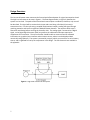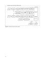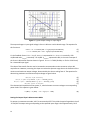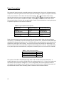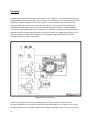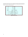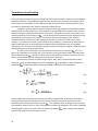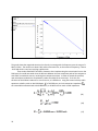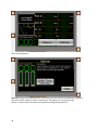
1
Indiana University-Purdue University Fort Wayne Department of Engineering ECE 406 Senior Design Project Report #2 Project Title: Low Cost RF Power Meter Team Members: Tom Wolf Brenton Weaver Evan Steinmetz Faculty Advisor: Dr. Abdullah Eroglu Date: May 11, 2013 1 Table of Contents: Table of Contents .............................................................. 2 Acknowledgement .............................................................. 4 Abstract/Summary .............................................................. 5 Section I: A Detailed Design of the Selected Conceptual Design Design Overview ....................................................... 7 Logarithmic Detector Microcontroller ................................................ 9 . . . . . . . . . . . . . . . . . . . . . . . . . . . . . . . . . . . . . . . . . . . . . . . . . . . . . . . 13 Ethernet Connectivity LCD Display ...................... 6 . . . . . . . . . . . . . . . . . . . . . . . . . . . . . . . . . . . . . . . . . . . . . . . . 15 . . . . . . . . . . . . . . . . . . . . . . . . . . . . . . . . . . . . . . . . . . . . . . . . . . . . . . . 16 Measurement and Calibration . . . . . . . . . . . . . . . . . . . . . . . . . . . . . . . . . . . . . . . . . 17 Interchangeable Four-Port Directional Coupler Measurement Accuracy . . . . . . . . 19 Software Capabilities . . . . . . . . . . . . . . . . . . . . . . . . . . . . . . . . . . . . . . . . . . . . . . . . 21 Accuracy Considerations . . . . . . . . . . . . . . . . . . . . . . . . . . . . . . . . . . . . . . . . . . . . . . . . 23 Power Consumption . . . . . . . . . . . . . . . . . . . . . . . . . . . . . . . . . . . . . . . . . . . . . . . . 25 Section II: Building Process . . . . . . . . . . . . . . . . . . . . . . . . . . . . . . . . . . . . . . . . . . . . . . . . 26 Schematic . . . . . . . . . . . . . . . . . . . . . . . . . . . . . . . . . . . . . . . . . . . . . . . . . . . . . . . 27 Printed Circuit Board PCB Design Considerations . . . . . . . . . . . . . . . . . . . . . . . . . . . . . . . . . . . . . . . . . 33 Transmission Lines/Coupling . . . . . . . . . . . . . . . . . . . . . . . . . . . . . . . . . . . . . . . . . 34 LCD Programming 2 . . . . . . . . . . . . . . . . . . . . . . . . . . . . . . . . . . . . . . . . . . . . . . . . 29 . . . . . . . . . . . . . . . . . . . . . . . . . . . . . . . . . . . . . . . . . . . . . . . . 36 GUI Coding Methodology . . . . . . . . . . . . . . . . . . . . . . . . . . . . . . . . . . . . . . . . . 41 Microcontroller Programming . . . . . . . . . . . . . . . . . . . . . . . . . . . . . . . . . . . . . . . . . 42 Enclosure . . . . . . . . . . . . . . . . . . . . . . . . . . . . . . . . . . . . . . . . . . . . . . . . . . . . . . 44 Bill of Materials . . . . . . . . . . . . . . . . . . . . . . . . . . . . . . . . . . . . . . . . . . . . . . . . . . . . . . 48 Section III: Testing . . . . . . . . . . . . . . . . . . . . . . . . . . . . . . . . . . . . . . . . . . . . . . . . . . . . . . 49 Requirements and Specifications . . . . . . . . . . . . . . . . . . . . . . . . . . . . . . . . . . 50 Scalar Procedure . . . . . . . . . . . . . . . . . . . . . . . . . . . . . . . . . . . . . . . . . . . . . . . 51 Data Measurements . . . . . . . . . . . . . . . . . . . . . . . . . . . . . . . . . . . . . . . . . . . . . . . 52 Calculation/Analysis . . . . . . . . . . . . . . . . . . . . . . . . . . . . . . . . . . . . . . . . . . . . . . . 61 Section IV: Evaluation and Recommendations Requirements Evaluation Recommendations . . . . . . . . . . . . . . . . . . . . . . . . . . . . . . . . . . 64 . . . . . . . . . . . . . . . . . . . . . . . . . . . . . . . . . . . . . . . . . 65 . . . . . . . . . . . . . . . . . . . . . . . . . . . . . . . . . . . . . . . . . . . . . . . 67 Conclusion . . . . . . . . . . . . . . . . . . . . . . . . . . . . . . . . . . . . . . . . . . . . . . . . . . . . . . . . . . . . 68 References . . . . . . . . . . . . . . . . . . . . . . . . . . . . . . . . . . . . . . . . . . . . . . . . . . . . . . . . . . . . 69 Appendix . . . . . . . . . . . . . . . . . . . . . . . . . . . . . . . . . . . . . . . . . . . . . . . . . . . . . . . . . . . . 70 A. Design Schematic . . . . . . . . . . . . . . . . . . . . . . . . . . . . . . . . . . . . . . . . . . . . . . . 70 B. Low Cost RF Power Meter User Manual 3 . . . . . . . . . . . . . . . . . . . . . . . . . . . 71 Acknowledgement: The Low Cost RF Power Meter Team would like to give a special thanks to Dr. Abdullah Eroglu, and the sponsorship of the IPFW RF/Microwave Lab, for his insight and guidance from an engineering perspective. His knowledge and expertise has been a great help and the primary source of advisement. A special thank you also goes to Advanced Circuits for their help in the etching and drilling of the printed circuit board, enabling us to finish on time. We would also like to thank the Applied Sciences Laboratory, and specifically Bob Tilsbury and Dave Campbell, who aided in the soldering of the PCB. Without the aid of all of these people, our project would not be a possibility. 4 Abstract/Summary: An low cost RF power meter was designed, as seen in Figure 1 below, utilizing the broadband capabilities of a scalar power meter a compatibility with all couplers within the defined range of 1 MHz to 6 GHz. The design is capable of measuring both the forward and reflected power measurements of a signal through a four port directional coupling system. The scalar power is able to be measured over the entire previously defined range. The design should enable this information is then communicated to the user through both an onboard display and web-hosted server, which can be viewed by internet browserenabled devices. 5 Section I: Detailed Design Description 6 Design Overview: The low cost RF power meter measures the forward and reflected power of a signal connected to a load. The high level overview can be seen in Figure 1. The flow diagram below, in Figure 2, identifies the system at a low level. The paths of the forward and reverse inputs are identical; therefore, only one will be described. The signal will be received at the input and travel along a 50 Ohm (Ω) microstrip transmission line. It is then split using a coupled line directional coupler, sending the signal through matching networks and into the Logarithmic Diode RF Power Detector. The output at both steps is filtered for antialiasing before entering the Controller Unit. The analog signal is converted to a digital signal, so the Digital Signal Processor (DSP) can perform the calibration techniques required to compensate for inaccuracies. The microcontroller should be able to communicate the calibrated information to a graphical user interface and an internet server, where it can be displayed both numerically and graphically. The system is powered by a supply, which can come from an AC or battery source, and is regulated for use by the components in the design. The full schematics are available in the appendix. Figure 1: High-level overview of the system. 7 Figure 2: Low-level overview of the system. 8 Logarithmic Detector: The AD8318 is a demodulating logarithmic amplifier, capable of accurately converting an RF input signal to a corresponding decibel-scaled output voltage. This device utilizes the progressive compression technique over a cascaded amplifier chain, each stage of which is equipped with a detector cell. The AD8318 maintains accurate log conformance for signals of 1 MHz to 6 GHz and provides useful operation up to 8GHz. The input range is 60 dB with error less than +/- 1 dB. The device provides exceptional logarithmic intercept stability vs. ambient temperature conditions. A 2 mV/C slope temperature sensor output is also provided for additional system monitoring. A single supply voltage of 5 V is required while current consumption is typically 68 mA. The AD8318 can be used as either a measurement or a controller device. As a measurement device, Pin VOUT is externally connected to VSET to produce an output voltage. VOUT is a decreasing linear-in-dB function of the RF input signal amplitude. The logarithmic slope is nominally -25 mV/dB, but can be adjusted by scaling the feedback voltage from VOUT to the VSET interface. The intercept is 20 dBm using the INHI input. Basic Connections The two positive supply pins, VPSI and VPSO, must be connected to the same positive potential between 4.5V – 5.5V. The two adjacent power supply pins can share a pair of decoupling capacitors (100 pF and .1 pF) power supply decoupling capacitors connect close to each power supply pin. Common pins CMOP and CMIP should be connected to a low impedance ground plane. The ENBL pin must be pulled high (> 1.7 V) to enable the device. The VOUT pins for both AD8318 devices will be connected to pins AN20 and AN21 on the dsPIC33FJ256GP710A. Input Signal Coupling The RF input to the AD8318 (INHI) is single ended and must be AC coupled. INLO is AC coupled to ground. Suggested coupling capacitors are 1 nF ceramic, 0402 style capacitors. At DC, the resistance is typically 2kΩ. At frequencies up to 1 GHz, the impedance is approximated as 1000 Ω||0.7 pF. While the input can be reactively matched, this is typically not necessary. An external 52.3 Ω shunt resistor combines with relatively high input impedance to provide an adequate 50 Ω match. The coupling time constant, 50x CC/2, forms a high-pass corner with a 3 dB attenuation at fHP = 1/(2π × 50 × CC ), where C1 = C2 = CC. Using the typical value of 1 nF, this high-pass corner is ~3.2 MHz. In high frequency applications, fHP should be as large as possible to minimize the coupling of unwanted low frequency signals. Setpoint Interface The setpoint interface is shown below in Figure 4. The VSET input drives the high impedance (250 kΩ) input of an internal operational amplifier. The VSET voltage appears across the internal 3.13 kΩ resistor to generate ISET. When a portion of VOUT is applied to VSET, the feedback loop forces (1) 9 If VSET = VOUT/X, ISET = VOUT/(X × 3.13 kΩ). The result is VOUT = (−ID × 3.13 kΩ × X) × log10(VIN/VINTERCEPT). The slope is therefore −ID × X × 3.13 kΩ = −500 mV × X. For example, if a resistor divider to ground is used to generate a VSET voltage of VOUT/2, X = 2. The slope is set to -1 V/decade or -50 mV/dB. Temperature Compensation of Output Voltage The AD8318 includes the capability to externally trim the temperature drift. RTADJ can be optimized for operation at different frequencies. The value of this resistor partially determines the magnitude of an analog correction coefficient that is employed to reduce intercept drift. Table 1 lists recommended resistors for various frequencies. Experimentation is required to choose the correct RTADJ resistors at frequencies not listed in Table 1. Table 1: Recommended RTADJ Resistors Temperature Sensor The AD8318 generates a voltage that is proportional to absolute temperature (VPTAT). This voltage is multiplied by a factor of 5, resulting in a 2 mV/C output at the TEMP pin. The temperature sensor output varies with output current due to increased die temperature. Output loads less than 1 kΩ draw enough current from the output stage causing this increase to occur. Measurement Mode When the VOUT voltage, or a portion of the VOUT voltage, is fed back to VSET, the device operates in measurement mode. As shown in Figure 3, the AD8318 has an offset voltage, a negative slope, and a VOUT measurement intercept greater than its input signal range. 10 Figure 3: Typical Output Voltage vs. Input Signal The output voltage vs. input signal voltage is linear-in-dB over a multi-decade range. The equation for this function is (2) (3) X is the feedback factor in VSET = VOUT/X. VINTERCEPT is expressed in Vrms. VSLOPE/DEC is nominally −500 mV/decade and VSLOPE/dB is nominally −25 mV/dB. VINTERCEPT, expressed in dBV, is the x-axis intercept of the linear-in-dB transfer function shown in Figure 4. VINTERCEPT is 7 dBV (20 dBm, re: 50 Ω or 2.239 Vrms) for a sinusoidal input signal. The slope of the transfer function can be increased to accommodate various converter mV per dB requirements. However, increasing this slope can reduce the dynamic range due to the limitation of the minimum and maximum output voltages, determined by the chosen scaling fator X. The equations for determining maximum and minimum output voltage are given below. (4) (5) (6) (7) The characteristic impedance of the system, Zo, must be known to convert voltages to corresponding power levels. This equation is given below. (8) Setting the Output Slope in Measurement Mode To operate in measurement mode, VOUT is connected to VSET. This yields the typical logarithmic slop of -25 mV/dB. The output swing corresponding to the specified input range is then approximately .5V to 11 2.1V. The slope and output swing can be increased by placing a resistor divider between VOUT and VSET. An example is shown below in Figure 4. Figure 4: Increasing the Slope The example shown in Figure 3 doubles the slope to approximately -50 mV/dB. Slope setting resistors should be kept below 50 kΩ. Output Filtering For applications which maximum video bandwidth and fast rise time are desired, it is essential that the CLPF pin be let unconnected and free of any stray capacitance. To reduce the nominal output video bandwidth of 45 MHz, connect a ground referenced capacitor (CFLT) to the CLPF pin. Generally this is done to reduce output ripple (at twice the input frequency for a symmetric input waveform, such as sinusoidal signals). CFLT is selected by the equation given below. - 1.5 pF (9) Set the video bandwidth to a frequency equal to about one tenth the minimum input frequency. This ensures that the output ripple of the demodulated log output, which is at twice the input frequency, is well filtered. The minimum input frequency (Video Bandwidth) is 1 MHz, therefore the CLPF is 1.0155 nF. 12 Microcontroller: The dsPIC33FJ256GP710A is part of the dsPIC33F General Purpose Family of devices that are ideal for a wide variety of 16-bit MCU applications. This device employs a powerful 16-bit architecture that integrates the control features of a Microcontroller with the computational capabilities of a Digital Signal Processor (DSP). The resulting functionality is ideal for applications that rely on high-speed, repetitive computations, as well as control. The dsPIC33FJ256GP710A is a 100 pin device with 256 Kbytes of Program Flash Memory, 30 Kbytes of RAM, 2 ADC 32 ch, and 85 I/O Pins. This CPU (Central Processing Unit) utilizes the DSP engine, dual 40-bit accumulators, hardware support for division operations, barrel shifter, 17 x 17 multiplier, a large array of 16-bit working registers and a wide variety of data addressing modes, together provide the device with extensive mathematical processing capability. Flexible and deterministic interrupt handling, coupled with a powerful array of peripherals make this device suitable for control applications. Basic Connection Requirements Getting started with the 16-bit Digital Signal Controller (DSCs) requires attention to a minimal set of device pin connections before proceeding with development. The following pin names must always be connected: 1. VDD and VSS 2. AVDD and AVSS (regardless if ADC module is used) 3. VCAP 4. MCLR 5. PGECx/PGEDx (In-Circuit Serial Programming) 6. OSC1 and OSC2 (When external oscillator used) 7. VREF+.VREF – (When external voltage reference for ADC module implemented) The use of decoupling capacitors (.1 uF) on every pair of power supply pins, such as VDD, VSS, AVDD, and AVSS is required. A low-ESR (< 5 Ohms) capacitor is required on the VCAP pin, which is used to stabilize the voltage regulator output voltage. The capacitor must be between 4.7 uF and 10 uF. The MCLR pin provides for the functions of device reset and device programming. The capacitor C will need to be isolated from the pin during programming and debugging operations. See Figure 5 below for proper use of the MCLR pin. 13 Figure 5: Example of MCLR Pin Connections The PGECx and PGEDx pins are used for In-Circuit Serial Programming and debugging purposes. Pull-up resistors, series diodes, and capacitors on these pins are not recommended. VREF+ / VREF- pins are connected to external voltages references for ADC functions. The AVDD and AVSS pins must be connected independent of the ADC voltage reference source. Unused I/O pins are configured as outputs and driven to a logic-low state. Alternatively, connect a 1K to 10K resistor between VSS and the unused pins. Analog-To-Digital Converter This device has up to 32 ADC input channels with up to 2 ADC modules, each with its own set of Special Function Registers. The 10-bit, 4-sample/hold ADC (default configuration) will be implemented. Pins AN20 and AN21 will be utilized as the analog inputs for the two AD8318 devices. The connections of all pins are found in the design schematic in Appendix A. I/O Ports All of the device pins (except VDD, VSS, MCLR and OSC1/CLKIN) are shared between the peripherals and the parallel I/O ports. To use a pin as a digital I/O pin on a shared ANx pin, the user application needs to configure the analog pin configuration registers in the ADC module, by setting the appropriate bit that corresponds to that I/O port pin to a ‘1’. Both analog pin configurations for both ADC modules must be configures as a digital I/O pin. Most I/O pins have multiple functions. The priorities of the functions allocated to any pins are indicated by reading the pin name from left to right on the data sheet. Pins RA0:RA7 are connected to pins AD0:AD7 on the mikroETH100 device. Pins RB0:RB14 are connected to pins A0:A14 on the mikroETH100. Pins RC0:RC2 will be connected to pins CS, RD and WR respectively. Universal Asynchronous Receiver Transmitter (UART) The UART module is a full duplex asynchronous system that can communicate with peripheral devices. This serial I/O module will be used to communicate with the µLCD-32PT. Pins U1RX and U1TX will be connected to pins TX and RX, respectively. 14 Ethernet Connectivity: Figure 6: Mikroelektronika’s 100Mbps mikroETH100 Ethernet Board, using Microchip’s ENC624J600 10/100 Base-T Ethernet controller. The Ethernet connection of the RF Power Meter will be accomplished with Mikroelektronika’s mikroETH100 standalone Ethernet board with Microchip’s 100Mbps ENC624J600 10/100 Base-T Ethernet controller. The ENC624J600 features integrated MAC and PHY, hardware cryptographic security engines, a factory programmed MAC address, and IEEE 802.3 compliancy. Microchip also offers a free TCP/IP stack with example code for all of their microcontrollers to utilize the ENC624J600. The ENC624J600 was selected primarily as a result of it being compatible with the dsPIC Digital Signal Controller (DSC). Additionally, Microchip offers a free embedded TCP/IP stack and example code for use with any of their microcontrollers. These free tools will allow a more rapid development of the embedded web server that is required to accomplish the remote connectivity of the design. Effective implementations can be accomplished with less than 34kB of code using this library, which leaves much of the 256kB of code in the microcontroller for other applications. The interface between the Ethernet controller and dsPIC is accomplished via a 16-bit Parallel Slave Port interface. The mikroETH100 Ethernet Board is a standalone package which includes all external components for the ENC624J600 to be utilized. This allows Ethernet connectivity to be quickly implemented into the design without requiring additional design time for the Ethernet controller module itself. Mikroelektronika also offers example code in C for Microchip microcontrollers to use this specific board. The entire board is powered by one 3.3V supply, and can be physically separated from the input stage of the meter to reduce the possibility of interference from the Ethernet connection in power measurements. The remote capability of the meter will be accomplished through an embedded web server on the dsPIC. When the meter is connected to the internet via the Ethernet interface, a user can remotely view a simple html web page on a web browser to gain access to measurement and configuration information, system status, and even to send commands to the meter remotely. One of the major benefits of this remote capability implementation is that no special software or hardware is needed to connect to the meter; any web-capable device can access the embedded web server. Microchip has several sample projects with code for many embedded internet applications using their microcontrollers and standalone Ethernet controllers. These free software resources will reduce the development time for the embedded web server by allowing a high-level design approach without needing to implement low-level stack protocols. 15 LCD Display: The user interface to the RF Power Meter will be accomplished with the µLCD-43PT(SGC) graphical TFT LCD module with resistive touch screen technology. The µLCD-43PT(SGC) is a standalone module featuring an embedded 4D-Labs PICASO-SGC graphics processor, which provides powerful graphic, text, imaging, and other features without taxing the main system microcontroller. The module communicates via a simple serial port interface to the host microcontroller, and commands are sent using a simple protocol. The display has an area of 95.0 x 53.9 mm with Figure 7: µLCD-43PT(SGC) graphical TFT LCD a 4.3” diagonal, and a 480 x 272 QVGA resolution with module with resistive touch screen technology. 65K colors. The touch capability is implemented with a 4-wire resistive touch panel. The µLCD-43PT(SGC) has many additional features such as a microSD memory card adapter for storing images or other data, and on-board audio with 8-Ohm speakers. The entire module includes four mounting tabs with 3mm holes for easy mounting in the application. The µLCD-43PT(SGC) module was chosen primarily for the high degree of standalone capability it offers. The PICASO-SGC graphics processor will allow a high-quality graphical user interface to be implemented with little microcontroller overhead code. The graphics processor has built-in high-level graphics functions and algorithms for drawing lines and circles, which will allow the plotting of various charts to visually display measurement data. The asynchronous serial TTL interface allows easy connection to the dsPIC microcontroller’s USART port. If additional memory is needed for displaying figures or pictures, such as a start-up logo, the on-board microSD memory card interface can be utilized. The touch-screen interface is another important feature of the display, as it eliminates the need for many hardware interface components in the design while improving the overall quality of the user interface. Less-used functions can be hidden within menu options, which will allow a less cluttered interface during normal operation. The four-wire resistive touch panel allows the use of both general touch and stylus use. All of the functionality of the µLCD-43PT(SGC) comes at a very reasonable price of only $140.00, which is less than some similar nonstandalone display-only products. There is a similar 3.2” µLCD display module which is less expensive than this 4.3 µLCD display, but the usefulness of the screen and touch capability are more significantly Figure 8: Back view of the hindered by the smaller screen size. The µLCD-43PT(SGC) is still µLCD-43PT(SGC) standalone cheaper than some display-only products of similar size. LCD touch screen module. 16 Measurement and Calibration: The scalar power detection for the Low Cost RF Power Meter will be performed using two of Analog Devices AD8318 MMICs. The AD8318 is a demodulating logarithmic amplifier, capable of accurately converting an RF input signal to a corresponding decibel-scaled output voltage. This device utilizes the progressive compression technique over a cascaded amplifier chain, each stage of which is equipped with a detector cell. The AD8318 maintains accurate log conformance for Figure 9: Typical AD8318 logarithmic amplifier signals of 1 MHz to 6 GHz and provides useful operation up to 8GHz. The input range is from response and error vs. input amplitude (5.8 GHz). -50 dBm to 0dBm, with error less than +/- 1 dB. When the VOUT voltage, or a portion of the VOUT voltage, is fed back to VSET, the device operates in measurement mode. As shown in Figure 9, the AD8318 has an offset voltage and a negative slope. The output voltage vs. input signal voltage is linear-in-dB over a multi-decade range. The equation for this function is given by Equations 11 and 12 below. (11) (12) The RF Power Meter must be correctly calibrated in order to make accurate absolute power measurements. One accessible way to perform this calibration is to use an RF source with a calibrated output power at known frequencies of interest, which will allow the calibration to be transferred to the RF Power Meter. The calibration procedure for a log-responding detector is fairly straightforward when the device is used in its linear range. Figure 9 shows the typical response of an AD8318 RF logarithmic amplifier based power detector IC at 5.8 GHz. It is clear that the slope of the output voltage is approximately linear with respect to the input power in dBm over a wide dynamic range. This allows the use of a relatively simple 2-point calibration scheme to capture the slope and intercept of the linear response of the detector at a specific frequency. The AD8318 is most linear from -50 dBm to 0 dBm, which offers a wide 50 dB measurement dynamic range. Calibrated attenuators may be needed in order to shift the calibrated power signal into the acceptable range of the AD8318 detectors. The 2-point calibration consists of inputting two known power levels at a given frequency to the power meter and recording the measured power levels. From the AD8318 datasheet, output voltage is related to input power by the equation: (13) 17 The calibration points must be chosen from within the linear region of the device (-50 to 0 dBm at most frequencies). The slope and intercept are then given by: (14) (15) When the slope and intercept have been calculated at a specific frequency, an unknown input power can be calculated based on the output voltage from the AD8318 using the equation: (16) These approximating slope-intercept equation parameters can then be calculated at different frequencies over the entire 1 MHz to 6 GHz frequency range and stored as a table in memory. The user will then be required to input the measurement frequency so that the meter can use the correct approximating equation to obtain the best measurement accuracy. The slope-intercept calibration will only need to be performed once as a device calibration, as opposed to an end-user calibration procedure. The only end-user calibration needed for absolute power measurements is a simple zeroing of the meter with a known power signal at the input. The zeroing term will be implemented as a simple modification to Equation 16, where an additional Zero term is added after the Intercept term to alter the intercept of the linear approximation so that the measured value matches the known calibration value. This intercept adjustment is easily extended to directional coupler measurements by using a known power source along with a known reflective load. The AD8318 has a nominal -24 mV/dB slope with a typical output voltage range of 0.5 V to 2.1 V. The dsPIC has a 12-bit ADC capability, and by using a 0 V to 2.5 V ADC range the size of the LSB is approximately 610 µV. By dividing the nominal slope by the LSB size, the digital resolution is given by: (17) With almost 40 LSB/dB digital resolution there is no need to scale the AD8318 output voltage to exactly fit the 0 V to 2.5 V range of the ADC. 18 Interchangeable Four-Port Directional Coupler Measurement Accuracy: In addition to the accuracy considerations of the AD8318 detectors, the interchangeable directional coupler at the front end of the system presents its own measurement uncertainties and calibration requirements. Most importantly, it is found that the directivity of the coupler is the most important parameter to its measurement accuracy. The following is the general S-parameter equation for in a directional coupler with the source at port 1 (P1), forward-coupled line at P3, reverse-coupled line at P2, and the load at P4. (18) (19) (20) – Forward coupled power from P1 to P3: very large compared to other signals. – This is multiplied by all power terms incident to P2 to give the contribution of this power to that incident to P3. – Power emergent from port 1 multiplied by gives power incident to P2 resulting from . – Note that , this is the power reflected from the DUT. So multiplied by gives the power incident to P2 resulting from . – This is the power incident to P3 resulting from reflected power at P3. With matched detector this is close to zero. – Power at P3 resulting from reflected power from the load/DUT. In a good directional coupler (high directivity) this is very small. Several properties of the directional coupler system can simplify the above equation. For highly matched detectors . Also, loose coupling gives since only a small amount of power is coupled. Finally, the coupler is also assumed to be a low-loss device, which gives . Also note that the coupling factor is and the directivity is related to the s-parameters as . These simplifications give: (21) √ √ √ [ | |√ √ | √ | ] (22) (23) The power at P3 is then given by squaring the magnitude of , which takes on a minimum and maximum value due to the two phases. The maximum is given when when the magnitudes are added, and the minimum occurs when the two components are 19 out of phase. | [ | √ ] (24) Similarly, the power at port P2 is found by using the s-parameter equation for simplifications: with the same (25) (26) | √ √ | √ √ [ √ (27) | | √ [| | √ √ ] (28) ] (29) In a reflectometer measurement, the reflected power reading is divided by the forward power reading, and the resulting fraction is square-rooted to give the reflection coefficient magnitude. This gives the following equation: | | √ | | √ | (30) | √ Which can be made clearer by pulling out a | term from the numerator: | | |[ | |√ | | ] (31) √ This equation clearly shows how the directivity and magnitude of the return loss ( ) can adversely affect the measurement accuracy of the reflection coefficient of the DUT. It is also clear that the forward measurement gains accuracy as return loss decreases, while the reverse measurement loses accuracy as return loss decreases. Higher coupler directivity increases accuracy in all cases. It is also important to note that both the coupling factor and the input power level have no influence on the measurement of the reflection coefficient magnitude. Therefore, these parameters may be adjusted to meet the requirements of the AD8318 detectors without affecting the measurement accuracy. One additional requirement is that the AD8318 detectors be closely matched to the 50 Ω system. However, the forward and reflected power measurements will require a simple calibration to correct for the coupling and the power supplied by the generator. A simple calibration procedure when using a directional coupler is to use a matched load condition to calculate the value of . With a constant-power generator this will be a constant value, and will allow the correction of both the forward and reverse measurements due to the coupling of the directional coupler. If desired, an additional fully reflective standard may be used to separately calibrate the reverse power measurement, but this is not directly required with a single directional coupler. 20 In the Low Cost RF Power Meter design, the coupler calibration correction will take place as a separate stage from the AD8318 calibration. This separation will simplify the calibration of the coupler, since only one power level from the generator is needed to characterize the coupling coefficient. The effects of the coupler directivity cannot be calibrated against, and must be taken into consideration by the RF engineer when choosing a coupler to measure an unknown load return loss. When measuring closely matched loads one should use a directional coupler with the highest available directivity to obtain accurate measurements. Software Capabilities: The embedded software is one of the more important components of the Low Cost RF Power Meter. Many of the high-level functions of the meter, such as the graphical user interface and Ethernet connection, are implemented in software running on the host microcontroller. Additionally, all signal processing performed after the two AD8318 logarithmic power detectors is performed digitally. Generally, these two sets of requirements would be met by separate digital signal processor and microcontroller chips, but these low-level DSP requirements in combination with higher-level control requirements are met well by the capabilities of the single chip dsPIC33FJ digital signal controller. The digital signal processing requirements are primarily determined by two factors: the averaging (filtering) of the measurements and the measurement calibration adjustment used to obtain the digital representation of power. The filtering requirements of the design are minimal due to the nature of the signal being measured. The low pass filtering before the sampling will be performed by the AD8318 detector chip. The capacitance connected to its input pin CPLF determines the maximum video bandwidth of the chip’s output, and will act as the anti-aliasing filter for the sampling process. The recommended video bandwidth from the AD8318 datasheet is 100 kHz based on the desired minimum input frequency of 1 MHz. This bandwidth will require a sampling frequency of at least 200ksps for each channel to meet the Nyquist rate. The raw sampled data will already have been low pass filtered at 100 kHz, and will be further smoothed by an adjustable averaging of the sampled values to obtain more accurate measurement results. Longer averaging times will yield more stability in the indicated power level, and may be necessary to compensate for noise in the measured RF signal itself. The calibration adjustments will be performed after the averaging of the sampled signals following equation 16 from the Measurement & Calibration section. The linear calibration adjustment involves one division and two addition operations to adjust each averaged measurement value. The first addition is for the intercept of the AD8318 transfer function, and the second addition is for the zeroing calibration value performed before measuring after powering on the meter. The calibration adjustment translates the voltage output from the detectors to a power measurement in dBm. The calculations of and VSWR will also be calculated, involving one division and two additions plus one division, respectively. The meter will also be responsible for hosting an embedded web server via an Ethernet connection and TCP/IP protocol stack implementation. The TCP/IP protocol and web server are free products from Microchip for their PIC microcontrollers and ENC standalone Ethernet controllers, and they will be implemented fully on the dsPIC. Additionally, the graphical user interface controls are handled by the dsPIC via a serial port connection to the graphical µLCD module. The low-level graphical functions and touch control calculations are handled by the µLCD module itself, so the primary software 21 load on the dsPIC from the display will be in menu navigation, input handling, and sending control signals for the display. The largest software load for the dsPIC will be from handling the embedded web server via TCP/IP and Ethernet. 22 Accuracy Considerations: The primary sources of error in the power measurement are associated with the AD8318 RF detectors and with the input terminations to the meter. The AD8318 is capable of a ±1.0 dB accuracy over a 55 dB dynamic range for frequencies less than 5.8 GHz. The range used in this design is from -50 dBm to 0 dBm, and the detectors maintain the ±1 dB accuracy beyond the 6 GHz requirement within this dynamic range. Additionally, the accuracy is increased when making relative power measurements due to the rejection of the common device error. The AD8318 also contributes to the error due to its imperfect conformity to the log-linear power to voltage response. The conformance varies based on power level and is worst at the extremes of the dynamic range below -55 dBm and above 0 dBm. Conformance also deviates with frequency, but calibration at each frequency accounts for this error if the frequency resolution of the calibration table is adequately high. Input impedance mismatch is another significant contributor to the overall error of the system. The internal input impedance to the AD8318 varies significantly with frequency, and is modeled by a resistance in parallel with a small capacitance. The capacitance stays consistently near 0.7 pF for the 1 MHz to 6 GHz frequency range, but the resistance varies from 1000 Ω at low frequencies down to less than 40 Ω at higher frequencies. The AD8318 datasheet suggests a shunt 52.3 Ω resistor to obtain a broadband 50 Ω match, but the return loss becomes significant at higher frequencies using this technique. A series of QUCS (Quite Universal Circuit Simulator) simulations were performed, as seen in Figure 10, to model the return loss of the AD8318 equivalent input impedances at several frequencies as supplied in the chip’s datasheet. Additionally, a best case simulation assuming a constant 1000 Ω resistive term was performed for the entire frequency range from 1 MHz to 6 GHz. Return loss approximates an exponential decay curve in the best case simulation, and is greater than 20 dB before 1 GHz. At 6GHz, however, the return loss approaches 6 dB. This indicates that at higher frequencies the AD8318 measurements will depend to some degree on the length of the measurement cables. The calibration procedure and startup zeroing will largely compensate for this error, but this underlines the importance of calibration accuracy in the accuracy of the final design. 23 Figure 10: QUCS simulation results for AD8318 return loss for the 1MHz – 6GHz frequency range assuming constant 100Ω||0.7pF equivalent input impedance to the AD8318. Capacitive coupling is used as recommended by the chip datasheet for a high pass cutoff of 1MHz. 24 Power Consumption: The system will require a supply to provide power to the components in the circuit. By observing each component’s maximum typical current draw and operational voltage, the power consumption of each IC is able to be calculated. This is done with the simple equation . The data sheets clearly describe the operational current range and voltage, usually and for the logarithmic detector, LCD module, microcontroller, and Ethernet module, respectively. These are found in Table 2 below. The maximum values of current and average Voltage are used in these calculations, ensuring the system is capable of operation at all intentional conditions. Table 2: Typical Operational Properties Component AD8318 µLCD-43PT(SGC) dsPIC33FJ256GP710A MikroETH 100 Supply Voltage (V) 4.5-5.5 4-5.5 3-3.6 3-3.6 Current Draw (mA) 50-82 (68 typ) 4-170 (150 typ) 30-90 82-117 Table 3 shows the total current at each of the typical operating voltages, along with the total power consumption. The AD8318, and µLCD-32PT(SGC) typically operate at 5 V, and the dsPIC33FJ256GP710A and MikroETH 100 typically operate at 3.3 V. The table uses the summed maximum current draw of the components requiring the same voltage. The total current used by the components demanding 5 V is 277 mA, and the total current used by the components demanding 3.3 V is 207 mA. Using these values in the power equation mentioned above, total power consumed by the circuit is shown to be 2.068 W. Table 3: Total Current and Power Total Current (max) @ 5 V 253 mA Total Current (max) @ 3.3 V 207 mA Total Power 1.948 W This system will be able to be powered through both a 120 V standard US outlet and batteries. A standard AA battery has a capacity of 2000 mAh with a voltage rating of 1.5 V. So four of will need to be connected in series to attain a voltage of 6 V. In this configuration, the current capacity will remain unchanged. After dividing the current capacity by total current draw, which is 484 mA, the system will be provided with about 4 hours of battery power at maximum current draw conditions. 25 Section II: Building Process 26 Schematic: The design was initially implemented in a schematic, as seen in Figure 11. This was completed using the program KiCAD to place all connections and form a general arrangement of the system components. The components include integrated circuits (IC’s), capacitors, resistors, headers, and input connections. Brenton created this schematic, with input from Tom and Evan, from research of the components’ datasheets and knowledge of the layout of the microcontroller peripheral ports. Voltage regulators were used to supply power to each of the components, as necessary. Headers of various sizes were also added to increase testability and to allow future expansion. Headers for voltage, ground, Ethernet, LCD, and programming connections were implemented. The programming header interfaces the dsPIC microcontroller with a PICkit 3 programmer. Figure 11: Design Schematic A netlist was then generated in order to map physical dimensions and pin connections of each schematic component for the layout of the printed circuit board (PCB) as seen in Figure 12. Here, each schematic component was assigned a footprint according to the package (shape, size, and pin count) of 27 each physical component that was chosen. The footprints for all capacitors and resistors were chosen as 0805 (0.079’’ x 0.049’’). The footprints for the AD8318, dsPIC, and voltage regulators have footprints of LFCSP_VQ, TSSOP, TQFP, and TO-220 respectively. Figure 12: Component Netlist 28 Printed Circuit Board: The printed circuit board features two copper layers, consisting of a ground plane and a top plane. Each surface mount component and through-hole component were mounted on the top layer. The majority of the copper traces used to connect the components are on the top plane. Traces implemented on the ground plane were necessary to make the most efficient use of the allotted area as well as to provide a means of “jumping” over other traces that may be in the way of making the desired connection. Vias were used to extend these traces from the top plane to the bottom plane. Unused areas on the bottom plane were filled to form the ground plane. Each trace has a width of 10 mils with the exception of the transmission lines, which are 26 mils. The board’s dielectric (core) is made of FR4 material with a thickness of 14 mils. Area restrictions of the housing required the PCB to have dimensions of 5’’x7’’. Small cutouts of .32’’ x .32’’ were implemented on the PCB design in order to fit the dimensions of the inside of the housing. The initial draft PCB design is shown in Figure 13. Each component was manually placed in order to make the most efficient use of the allotted space. Using the rats nests (visual representation of pin to pin connections), each trace was manually routed between all pins to complete the desired node, or connection. The upper right and left corners of the PCB (outlined in white) are reserved to allow space for the Ethernet module and the battery holder. The two AD8318s are oriented symmetrically on the left and right with the dsPIC located at the center Both voltage regulators are placed near the top center of the board. 29 Figure 13: Initial PCB Layout The Gerber files were sent to Advanced Circuits for the production of the final PCB design to be used. This PCB is displayed in Figure 14. A green soldermask was placed over all bare copper traces. White silkscreens were used to define the shape and the name of each component which is to be soldered. The bare copper patches on the board are places for each pin or surface mount component to be soldered. All circular copper rings are used for the soldering of through-hole components. The small diamond shape copper patches on the upper half of the board is call thieving. Thieving is copper that is left on open areas of a PCB in order to make the board easier to manufacture. 30 Figure 14: Top Layer of Final PCB Figure 15 shows the back side, or ground plane, of the PCB. All nine bottom layer traces can be seen from this view. Each trace starts and ends on a via, which extends the connection to the top copper layer of the board. All other areas make up the ground plane. This provides convenient ground connections to components from the top copper layer. Figure 15: Bottom Layer of Final PCB Figure 16 displays the PCB with all surface mount and through-hole components soldered. All components, with the exception of the dsPIC, were mounted by applying solder paste to each pad and then baking the board in a reflow oven to complete all pin to pad connections. The dsPIC was hand soldered using a microscope. The dsPIC (center) and AD8318s (left and right) were placed with special 31 care, as these devices are typically not soldered by hand. The right most AD8318 required several new applications of solder to ensure a proper connection of each pin. The dsPIC initially had a solder bridge across VDD and GND pin, which was removed to allow proper powering of the device. Labels were placed to allow easy and proper connection to the programmer (PICkit 3), power, and the LCD screen. Figure 17: Final PCB with all components soldered. 32 PCB Design Considerations: After soldering and testing our board, several PCB design errors were found. These errors include incorrect pinouts for both voltage regulator footprints, an unconnected VDD pin on each AD8318. As seen in Figure 16 above, a small grey board is used to interface the pins of the 5V regulator the orientations which was implemented on the PCB. A separate 3.3V regulator was implemented on a separate small breakaway board and was easily connected to the 3.3V header. Small wires were used to jump 5V to the unconnected power pins of both AD8318s. Although a new PCB was unable to be printed, the final PCB was modified in KiCAD to correct for these errors in the case that a new board would be printed in the future for this design. Figure 18 displays the most updated PCB design, which corrects for the errors found when the design was tested. Figure 18: Updated PCB Design 33 Transmission Lines/Coupling: The meter required a transmission line leading from the N-type connectors to the input of the AD8318 Logarithmic Detector. This enabled the signal to reach the circuit from the input of the device with as little insertion loss as possible. A microstrip was etched onto the printed circuit board (PCB) to act as the necessary transmission line, requires matching to reduce the loss. Impedance matching with a microstrip was performed using properties of the PCB to match an impedance equal to that of the input. These properties include the dielectric constant of the material between the copper plates and the thickness of the board. The dielectric constant, also known as the relative permittivity of the material, or , can be found from the data sheets of the PCB and can also vary based on the frequency of the signal. The material used in this project was FR-4, which is a composite material composed of woven fiberglass cloth with an epoxy resin binder that is flame resistant. This is the most common material used for PCB’s; however, its performance varies more at higher frequencies than its more expensive counterparts from manufacturers such as the Rogers Corporation. This variance is not significant enough at the chosen frequency range of 1 MHz to 6 GHz to radically affect the sensitivity of the material. The PCB’s used in this project, are from LPKF Laser & Electronics, and have a of 4.7 at 1 MHz, 4.35 at 500 MHz, and 4.34 at 1 GHz. These values are the typical points listed in the data sheets, which indicate that the stabilizes at a lower value as the frequency increases. Because of this, the value 4.35 was chosen to be the average permittivity used in simulation. The simulation, done in the Sonnet Project Editor, was used to test the performance of the microstrip. Using the following equations, with a PCB depth, , of 0.14986 cm, and a characteristic impedance, , the width was determined to be 0.28946 cm to match a 50 Ω impedance. = 1.52139 (32) (33) (34) Once the width was calculated, the simulation was able to be performed, selecting a material with a relative permittivity mentioned above and a loss tangent of 0.017, which was taken from the PCB specification sheet at the same frequency as the . For simulation sake, the length of the microstrip was arbitrarily chosen to be 1 cm, since its length does not affect the impedance. The results yielded the following graph in Figure 19, which shows the network parameter , which is equal to the negative insertion loss in dB, versus the frequency in GHz. 34 Figure 19: Sonnet simulation of the insertion loss versus frequency of the microstrip transmission line. The graph shows the magnitude insertion loss linearly increasing with the frequency over the range of 1 MHz to 6 GHz. The minimum is about 0 dB, and the maximum loss, at the maximum frequency, is about -0.155 dB, which is very low, implying a good match. These results worked for simulation; however, when implementing the transmission lines on the PCB layout, the width was wider than the distance between the two component pads of the component with which it needed to connect, rendering that component useless. In order to amend this problem, new calculations needed to be completed to reduce the width of the microstrip. To do this, the thickness of the PCB was reduced to a size of 14 mils, or 0.35560 mm. Using the same microstrip width equations as before, with an ideal PCB depth, , of 0.35560 mm, and a characteristic impedance, the new width was determined to be 0.68568 mm, or 26.9953 mils to match a 50 Ω impedance. (35) (36) (37) 35 , After the ideal calculation, QUCS was used to account for the thickness of the copper plating, instead of assuming a conductor with negligible thickness. The results yielded a width of 26.4082 mils, which was reduced to a realizable 26 mils. This simplification increased the impedance to 50.4589 Ω, and therefore only slightly reduced the accuracy of the system impedance match. LCD Programming: The graphical user interface of the uLCD43-PT touch-enabled display module was programmed using the 4D Systems Workshop4 integrated development environment. The necessary components for development include: uLCD module from 4D Systems micro-SD memory card with adapter to connect to PC USB to serial adapter cable Workshop4 IDE software PC with Windows operating system The Workshop4 IDE supports four different environments for the design of the LCD GUI. The Serial environment allows for developing of serial interface code for the LCD to be completely controlled by a host microcontroller. The Designer environment allows for direct programming of the LCD in its native 4dgl graphical programming language. The ViSi environment is a visual programming environment that allows for the use of pre-set display objects, such as buttons, keypads, textboxes, etc., along with programming in 4dgl. The ViSi Genie environment allows for purely visual programming of the LCD interface, which eliminates the need to implement 4dgl code for simple interfaces. Both ViSi environments include a virtual representation of the screen image to give a preview of what the LCD module will look like when programmed. The ViSi Genie environment was used to program the GUI for Low Cost RF Power Meter, because it allowed for rapid prototyping by virtually eliminating the learning curve. Additionally, the code can easily be ported into the ViSi environment to add more complicated objects or behavior to the display in future development. ViSi genie simplifies the programming to a set of Properties and Events associated with each object on the screen. The readings screen is shown in Figure 20 below. 36 Figure 20: Example of GUI development using ViSi Genie. The “Measure” button is currently selected,and the Event “OnChanged” is set to the Handler “Report Message” in the Object Inspector menu to the right of the image. Several of the pre-built graphical objects are shown on the screen image in Figure 20. These include buttons, digits, a gauge, plain text, and string text. The screen itself, known as a Form, is also an object, and it contains all objects placed on it. The design uses five separate forms to make up the GUI for the displayed readings and for the calibration routines. Each of the forms is shown in the figures below. Figure 21: Image of the welcome screen for the design. This is displayed for a few seconds as the device is powered on. 37 Figure 22: Image of the readings screen for the design. This is where each reading is displayed when measuring power. Figure 23: Image of the calibrate screen. This is where the user inputs the measurement frequency and selects which calibration he/she is performing. The frequency is set using the slider objects on the left, where each slider corresponds to the digit directly above it. 38 Figure 24: Image of the scalar power calibration screen. The system uses this screen to guide the user through the scalar calibration routine described in the Measurement and Calibration description from Section 1. The user inputs data using the custom-designed keypad on the left of the screen. All interactive objects on each LCD Form are configured to send a message over the serial UART line to the host dsPIC microcontroller. Messages are formatted as 6 byte message packets containing all needed information plus a checksum byte. The message type indicates if a command is being sent to the LCD or if the LCD is reporting an event (and what kind of event is being reported). The object type indicates what type of object (i.e. button, slider, digits, etc.) the message is about. The object index determines which instance of the indicated object type the message is about. The data value is a 16-bit integer containing the data for or from the specified object. The data value will contain different values for each different type of object. Finally, the checksum is an 8-bit XOR based checksum value to allow any transmission errors to be detected. message type byte 1 object type ID byte 2 object index byte 3 data value byte 4 byte 5 checksum byte 6 Programming and Validation The uLCD43-PT is programmed using the following procedure: 1. Connect the LCD module to the PC using the serial to USB adapter cable 2. Connect the micro-SD memory card to the PC using a USB or SD adapter 3. Start the Workshop4 IDE and open the project 4. Use the Comms ribbon to connect to the LCD 5. Press the “Build” button on the home ribbon in the Workshop4 IDE 6. When prompted, specify that the program be saved to the micro-SD card being used 7. Insert the programmed micro-SD card into the programmed LCD, keeping the LCD connected 39 To validate the program, go to the Tools menu and click on the GTX icon to open the Genie Test Tool. The GTX tool is used to send and receive serial messages from the LCD module to test the functionality of each object. Also, the message packet can be associated with each object and recorded for use in the microcontroller message decoding function. A screenshot of a GTX testing session is shown in Figure 25 below. Figure 25: Screenshot of a GTX test session in progress. The sent (green) and received (red) message packets are listed to the right, and a visual representation of the state of each LCD object is shown on the left. 40 GUI Coding Methodology: The code to handle the interface with the uLCD43-PT display module was developed largely before the system hardware was implemented on the printed circuit board. To mitigate the delay in the software development cycle, a solution was devised to allow coding and testing of the interface without the PCB hardware. The solution was to code the entire LCD interface in C code on a PC running Linux, using the USB to serial programming cable that was used to program the LCD module itself. This allowed for direct portability of most of the code to the dsPIC, which is also programmed in C. Only the low-level UART interface functions needed to be changed to run the code on the dsPIC, while all higher functionality was unchanged. This single design decision allowed for the prototype hardware to be tested and debugged within one week of receiving the PCB hardware, as very little time was spent in porting the fully tested interface code. 41 Microcontroller Programming: The dsPIC33FG256FJ710A is responsible for communication between all of the primary components, as well as the calculations of all calibration procedures. The first feature to be addressed in the programming of the microcontroller was the UART communication with the uLCD module. Much of the calibration code was initially tested on the LCD, so once communication was established, testing was able to be performed using the detectors’ voltage output. The UART was configured at 9600 Baud with 8-bit data transmission with 1 stop bit. Polling was used to determine when data is ready to be sent, ready to be read, or in the process of either. These are the basic functions utilizing the serial port, but other functions which employ these have been designed to work in conjunction with the LCD. The dsPIC receives the user inputs from the LCD and performs calculations based on these inputs. It first determines if a screen change is required. If not, then it determines which button was pressed on the keypad. The resulting action is then transmitted back to the module, such as which screen should be displayed, as well as the location and value of numerical data. Whenever a key is pressed, it is the controller’s responsibility to transmit the string of numbers that should be displayed in the readout. The ADC was the next major feature implemented in the dsPIC. It was configured with 10-bit conversion operation, and sequentially samples pins AN0, AN1, AN4, and AN5 with Channel 0 of ADC module 1, where pins AN0 and AN1 are receiving from the AD8318. This is configured for use with the DMA, which is configured in peripheral indirect and ping-pong modes. In these modes each peripheral determines its own address in data memory, and the ADC switches between these addresses for each pin sampled. The basic layout of the DMA can be found in Figure 26. When measuring phase and scalar power, the dsPIC interprets the analog voltage being sent from the detectors into integer values, which are then converted into variables holding the non-integer voltage value. Since the detectors transmit at a near DC level, the speed of the sampling is not a vital part of the design. It samples at about 200 kHz at each channel, which is well above the necessary rate, so no information is lost. Then the microcontroller utilizes the onboard DMA functionality to send the received values directly to data memory. Calibration techniques are performed, and the calibrated data is transmitted to be displayed on the uLCD module. The microcontroller is capable of communicating the MikroETH100, however, there was not time to develop and implement this feature. All of the code described in this section is able to be found in the appendix. 42 Figure 26: DMA diagram, describing the communication between the memory and peripherals that access it. 43 Enclosure: An enclosure was necessary to mount the LCD display, PCB, Ethernet port, and RF inputs. A housing that looked aesthetically pleasing that was within budget was also preferable. An housing of dimensions 8.740’’ L x 5.740’’ W x 2.960’’ H manufactured by Bud Industries was purchased from Digikey Corporation to be modified as the enclosure for the entire system. Figure 27 displays the product photo of the enclosure. Figure 27: Product photo of the enclosure. Cutouts were necessary for an Ethernet port, LCD, N-type connectors, DC power jack, and rubber feet. Drawings and specifications, found in Figures 28 through 30, were created and sent to the IPFW machine shop for modifications. Figure 28 below displays every view of the desired cutouts. The LCD screen cutout is shown on the top view, the DC power input cutout is shown on the back view, the Ethernet panel mount connector cutout is shown on the left view, and the two N-type connector cutouts are shown on the front view. The final result of the enclosure is shown in Figures 31 and Figure 32. 44 Figure 37: All views of the modified housing. Figure 38: Top view and front view cutout dimensions of the enclosure. 45 Figure 28: Cutout dimensions for the Ethernet panel mount connector and DC power jack. Figure 29: Final enclosure modification with mounted components. 46 Figure 41: Inside view of the enclosure. 47 Bill of Materials: The original budget of this design was $500 dollars, which is much less than nearly all of its competitors. Because of this limited allowance, and the importance of the RF signal integrity, designing a printed circuit board was important. Using development boards, such as Arduinos, were out of the price range, so surface mounted parts, such as the dsPIC33F microcontroller, were selected for placement on the board. Aside from these components, two peripheral modules, the uLCD and MikroETH100, were bought for ease of use, with simple UART and digital I/O communication, respectively. These were the most expensive components purchased, costing a total of $163. The real cost, however, came from the building of the PCB itself. Due to the necessity for quick completion and transportation, this cost the most, at $185. Table 4: Bill of materials for the final design. Item Part Number Quantity to Order Unit Price mikroETH100 Board mikroETH100 Board 1 $ 24.00 $ 24.00 uLCD ΜLCD-43PT(SGC) 1 $ 139.00 $ 139.00 Caps and Resistors N/A N/A N/A $ 1.89 Mouser Housing 377-1131-ND 1 $ 28.60 $ 28.60 Digikey Corporation Rubber Feet 720K-ND 4 $ 0.28 $ 1.12 Digikey Corporation Barrel Connector CP-067A-ND 1 $ 2.14 $ 2.14 Digikey Corporation Wall Wart 237-1421-ND 1 $ 5.79 $ 5.79 Digikey Corporation AD8318 AD8318ACPZ-REEL7CT-ND 2 $ 10.77 $ 21.54 Digikey Corporation 3.3 V Regulator LP3985IM5-4.7/NOPBCT-ND 1 $ 0.63 $ 0.63 Digikey Corporation dsPIC33F dsPIC33FJ256GP710A 1 $ 8.06 $ 8.06 Digikey Corporation Caps and Resistors N/A N/A N/A $ 1.45 Digikey Corporation Coax Connector PE44398 3 $ 19.71 $ 59.13 Pasternack 6-pin male header HEADS6 1 $ 0.70 $ 0.70 Futurlec 14x2 pin male header HEADD14 1 $ 1.70 $ 1.70 Futurlec F-F Jumper Wire 50pc 1700 1 $ 12.49 $ 12.49 Pololu Panel Mount RJ45 P115 ETHERNET RJ45 - PANEL F TO M 1 $ 10.00 $ 10.00 Frontx 5 V Regulator LM2937ET 2 $ 1.50 $ 3.00 Solarbotics PCB PCB 1 $ 185.00 $ 185.00 48 Total Cost Supplier MikroElektronika 4dsystems Advanced Circuits Section III: Testing 49 Requirements and Specifications: The requirements of the system are described below in Table 5. Most of these were developed in the first semester. Table 5: # 1 2 3 4 5 6 7 8 9 10 11 12 13 14 15 16 17 18 19 20 21 Requirements The system shall perform operations on signals between 1 MHz and 6 GHz. The system shall detect power signals between -50 dBm and 0 dBm. The system shall be able to measure the magnitude of the reflection coefficient. The system shall have an accuracy of ±0.5%. The system shall be operable between 0 C and -50 C. The system shall be able to be programmed. The system shall have a user interface. The system shall output information visually on a display. The system shall be able to interface and accept input from RF sources. The system shall be able to operate with power from both AC and battery sources. The system shall utilize a microcontroller. The system shall have a coupler containment system. The system shall have a standard connect to interface with most couplers The system shall have a durable and professional-looking housing. The system shall be small enough to be portable. The system shall have a sampling rate of twice the Nyquist frequency. The resolution of the system shall not negatively affect the accuracy. The system shall be built at a cost of under $500. The system shall have internet connectivity through Ethernet. The system shall be safe to use. The system shall be completed by the May 15, 2013. Scalar Procedure: 50 The system was tested using a Hewlett Packard 8648A signal generator, a Hewlett Packard 8595E spectrum analyzer, a Mini-Circuits 20dBm 30 – 400 MHz coupler, a ENI 603L 40 dB RF Power Amplifier, and an Agilent calibration kit. The equipment available, limited by the coupler in use, allowed for a narrow band of testing to be performed, so the device was tested from 100 MHz to 400 MHz, at 100 MHz intervals, and from -50 dBm to 0 dBm. The power level at the input of the test environment was actually -70 dBm to -20 dBm; however the attenuation of the system amplified the signal by 20 dB, bringing the levels within the operational range. The system was calibrated and then test measurements were made. A brief generalization of the calibration procedure is below, and a detailed instruction guide can be found in the appendix. 1) Input Signal of Known Power and Frequency 2) Measure Real Power with Known Loads (Matched, Open, and Short) 3) Mathematical Calibration (performed by microcontroller) 4) Attach DUT and Measure Power 5) Compare Measured Power to Real Power The first tests were calibrated directly from the signal generator, without the coupler. Calibration points were -40 dBm and -10 dBm, respectively, for linearity. By doing this, the power meter only displays the measured power coming out of the coupler. After reading the in the data, it is plotted and fit with a trend line. The intercept of this trend line is then used as the system attenuation, which is added to the generated signal level for the P_src_sys, which is the power going into the coupler. This value is calculated without the results from the -70 dBm readings. This is because it is very close to the design’s outer limit, and causes less linear results. The readings are compared to the system power for accuracy calculations. The second tests are calibrated including everything in the system. The readings from this test procedure relate to the power being input into the entire system, before attenuation, not just coming out of the coupler. The readings are compared to the input power for accuracy calculations. The calibration points used are -65 dBm and -35 dBm, respectively, for linearity. After calibration, the measurements were taken with two different loads. First, the incident and reflected signals with a matched load were measured, and then the same signals were measured with a 2:1 impedance mismatched load. Depending on the type of calibration implemented, the measured values are compared to either the signal from the generator or the signal coming out of the coupler. For both sets of results, the |Γ| is calculated from the mismatched load, where The results of these scalar tests are shown in the Data/Measurements section. Data/Measurements: 51 . The measured data is recorded in the tables below. Scalar measurements were taken after calibrating directly from the signal generator, without including the attenuation of the amplifier or the coupler, and then they were taken after calibrating the whole system, including the attenuation of the amplifier and coupler. There are two sets of data, both over the same frequency and source power ranges; however, Tables 6-9 were measured after calibrating the meter directly from the signal generator, without attenuation, while Table 10-13 were measured after calibrating the meter along with all attenuation included. While the measurements read on the forward port are comparable to the signal being sent by the generator, the reverse port cannot be related similarly. When measuring the reverse port of a matched load, it is ideally 0 mW, so it is always measured as very low, or too low to be in the range of measurability. 52 Table 6: Scalar test results after calibrating directly from the signal generator, without including the attenuation of the amplifier and coupler. These readings were taken at 100 MHz, over the power range of -70 dBm to -20 dBm from the signal generator. P1 and P2 for calibration were -40 and -10, respectively coming from the generator directly into the meter. Tests were performed with the whole system. Freq. (MHz) 100 100 100 100 100 100 100 100 100 100 100 100 100 100 100 100 100 100 100 100 100 100 100 100 Port F R F R F R F R F R F R F R F R F R F R F R F R 53 Load Matched Matched 2:1 2:1 Matched Matched 2:1 2:1 Matched Matched 2:1 2:1 Matched Matched 2:1 2:1 Matched Matched 2:1 2:1 Matched Matched 2:1 2:1 P_src (dBm) -70 -70 -70 -70 -60 -60 -60 -60 -50 -50 -50 -50 -40 -40 -40 -40 -30 -30 -30 -30 -20 -20 -20 -20 Amp. (dB) 40 40 40 40 40 40 40 40 40 40 40 40 40 40 40 40 40 40 40 40 40 40 40 40 Cpl (dB) 20 20 20 20 20 20 20 20 20 20 20 20 20 20 20 20 20 20 20 20 20 20 20 20 Sys. (dB) 14.054 14.054 14.054 14.054 14.054 14.054 14.054 14.054 14.054 14.054 14.054 14.054 14.054 14.054 14.054 14.054 14.054 14.054 14.054 14.054 14.054 14.054 14.054 14.054 P_src_sys -55.946 -55.946 -55.946 -55.946 -45.946 -45.946 -45.946 -45.946 -35.946 -35.946 -35.946 -35.946 -25.946 -25.946 -25.946 -25.946 -15.946 -15.946 -15.946 -15.946 -5.946 -5.946 -5.946 -5.946 P_meas (dBm) -51.39 N/A -51.51 N/A -44.93 N/A -45.82 -53.46 -35.44 -57.3 -36.45 -44.74 -25.69 -50.89 -26.58 -35.25 -15.69 -41.92 -16.7 -25.51 -5.44 -32.17 -6.45 -15.51 Abs. Error (dBm) -4.556 -4.436 -1.016 -0.126 -0.506 0.504 -0.256 0.634 -0.256 0.754 -0.506 0.504 - |Γ| N/A 0.414954 0.385035 0.368553 0.36266 0.352371 - Error dBm (%) 8.143567 N/A 7.929074 N/A 2.211292 N/A 0.274235 N/A 1.407667 N/A 1.402103 N/A 0.986665 N/A 2.443537 N/A 1.605418 N/A 4.728459 N/A 8.509923 N/A 8.476287 N/A Pcal1 (dBm) -40 -40 -40 -40 -40 -40 -40 -40 -40 -40 -40 -40 -40 -40 -40 -40 -40 -40 -40 -40 -40 -40 -40 -40 Pcal2 (dBm) -10 -10 -10 -10 -10 -10 -10 -10 -10 -10 -10 -10 -10 -10 -10 -10 -10 -10 -10 -10 -10 -10 -10 -10 Table 7: Scalar test results after calibrating directly from the signal generator, without including the attenuation of the amplifier and coupler. These readings were taken at 200 MHz, over the power range of -70 dBm to -20 dBm from the signal generator. P1 and P2 for calibration were -40 and -10, respectively coming from the generator directly into the meter. Tests were performed with the whole system. Freq. (MHz) 200 200 200 200 200 200 200 200 200 200 200 200 200 200 200 200 200 200 200 200 200 200 200 200 Port F R F R F R F R F R F R F R F R F R F R F R F R 54 Load Matched Matched 2:1 2:1 Matched Matched 2:1 2:1 Matched Matched 2:1 2:1 Matched Matched 2:1 2:1 Matched Matched 2:1 2:1 Matched Matched 2:1 2:1 P_src (dBm) -70 -70 -70 -70 -60 -60 -60 -60 -50 -50 -50 -50 -40 -40 -40 -40 -30 -30 -30 -30 -20 -20 -20 -20 Amp. (dB) 40 40 40 40 40 40 40 40 40 40 40 40 40 40 40 40 40 40 40 40 40 40 40 40 Cpl (dB) 20 20 20 20 20 20 20 20 20 20 20 20 20 20 20 20 20 20 20 20 20 20 20 20 Sys. (dB) 15.402 15.402 15.402 15.402 15.402 15.402 15.402 15.402 15.402 15.402 15.402 15.402 15.402 15.402 15.402 15.402 15.402 15.402 15.402 15.402 15.402 15.402 15.402 15.402 P_src_sys -54.598 -54.598 -54.598 -54.598 -44.598 -44.598 -44.598 -44.598 -34.598 -34.598 -34.598 -34.598 -24.598 -24.598 -24.598 -24.598 -14.598 -14.598 -14.598 -14.598 -4.598 -4.598 -4.598 -4.598 P_meas (dBm) -50.63 N/A -51.13 N/A -43.67 N/A -44.68 -52.12 -34.05 -53.91 -35.18 -43.19 -24.3 -45.61 -25.44 -33.48 -14.3 -35.53 -15.44 -23.65 -4.17 -25.57 -5.06 -13.57 Abs. Error (dBm) -3.968 -3.468 -0.928 0.082 -0.548 0.582 -0.298 0.842 -0.298 0.842 -0.428 0.462 - |Γ| N/A 0.42462 0.397649 0.396278 0.388597 0.375405 - Error dBm (%) 7.267665 N/A 6.351881 N/A 2.080811 N/A 0.183865 N/A 1.583907 N/A 1.682178 N/A 1.211481 N/A 3.423043 N/A 2.041376 N/A 5.767913 N/A 9.308395 N/A 10.04785 N/A Pcal1 (dBm) -40 -40 -40 -40 -40 -40 -40 -40 -40 -40 -40 -40 -40 -40 -40 -40 -40 -40 -40 -40 -40 -40 -40 -40 Pcal2 (dBm) -10 -10 -10 -10 -10 -10 -10 -10 -10 -10 -10 -10 -10 -10 -10 -10 -10 -10 -10 -10 -10 -10 -10 -10 Table 8: Scalar test results after calibrating directly from the signal generator, without including the attenuation of the amplifier and coupler. These readings were taken at 300 MHz, over the power range of -70 dBm to -20 dBm from the signal generator. P1 and P2 for calibration were -40 and -10, respectively coming from the generator directly into the meter. Tests were performed with the whole system. Freq. (MHz) 300 300 300 300 300 300 300 300 300 300 300 300 300 300 300 300 300 300 300 300 300 300 300 300 Port F R F R F R F R F R F R F R F R F R F R F R F R 55 Load Matched Matched 2:1 2:1 Matched Matched 2:1 2:1 Matched Matched 2:1 2:1 Matched Matched 2:1 2:1 Matched Matched 2:1 2:1 Matched Matched 2:1 2:1 P_src (dBm) -70 -70 -70 -70 -60 -60 -60 -60 -50 -50 -50 -50 -40 -40 -40 -40 -30 -30 -30 -30 -20 -20 -20 -20 Amp. (dB) 40 40 40 40 40 40 40 40 40 40 40 40 40 40 40 40 40 40 40 40 40 40 40 40 Cpl (dB) 20 20 20 20 20 20 20 20 20 20 20 20 20 20 20 20 20 20 20 20 20 20 20 20 Sys. (dB) 16.85 16.85 16.85 16.85 16.85 16.85 16.85 16.85 16.85 16.85 16.85 16.85 16.85 16.85 16.85 16.85 16.85 16.85 16.85 16.85 16.85 16.85 16.85 16.85 P_src_sys -53.15 -53.15 -53.15 -53.15 -43.15 -43.15 -43.15 -43.15 -33.15 -33.15 -33.15 -33.15 -23.15 -23.15 -23.15 -23.15 -13.15 -13.15 -13.15 -13.15 -3.15 -3.15 -3.15 -3.15 P_meas (dBm) -50.29 N/A -50.67 N/A -42.54 N/A -43.43 -52.56 -32.75 -50.64 -33.77 -43.58 -22.96 -41.28 -23.85 -33.71 -12.92 -31.41 -13.81 -23.97 -2.88 -21.41 -3.77 -13.97 Abs. Error (dBm) -2.86 -2.48 -0.61 0.28 -0.4 0.62 -0.19 0.7 -0.23 0.66 -0.27 0.62 - |Γ| N/A 0.349543 0.323221 0.321366 0.310456 0.30903 - Error dBm (%) 5.380997 N/A 4.66604 N/A 1.413673 N/A 0.648899 N/A 1.206637 N/A 1.870287 N/A 0.820734 N/A 3.023758 N/A 1.749049 N/A 5.019011 N/A 8.571429 N/A 19.68254 N/A Pcal1 (dBm) -40 -40 -40 -40 -40 -40 -40 -40 -40 -40 -40 -40 -40 -40 -40 -40 -40 -40 -40 -40 -40 -40 -40 -40 Pcal2 (dBm) -10 -10 -10 -10 -10 -10 -10 -10 -10 -10 -10 -10 -10 -10 -10 -10 -10 -10 -10 -10 -10 -10 -10 -10 Table 9: Scalar test results after calibrating directly from the signal generator, without including the attenuation of the amplifier and coupler. These readings were taken at 400 MHz, over the power range of -70 dBm to -20 dBm from the signal generator. P1 and P2 for calibration were -40 and -10, respectively coming from the generator directly into the meter. Tests were performed with the whole system. Freq. (MHz) 400 400 400 400 400 400 400 400 400 400 400 400 400 400 400 400 400 400 400 400 400 400 400 400 Port F R F R F R F R F R F R F R F R F R F R F R F R 56 Load Matched Matched 2:1 2:1 Matched Matched 2:1 2:1 Matched Matched 2:1 2:1 Matched Matched 2:1 2:1 Matched Matched 2:1 2:1 Matched Matched 2:1 2:1 P_src (dBm) -70 -70 -70 -70 -60 -60 -60 -60 -50 -50 -50 -50 -40 -40 -40 -40 -30 -30 -30 -30 -20 -20 -20 -20 Amp. (dB) 40 40 40 40 40 40 40 40 40 40 40 40 40 40 40 40 40 40 40 40 40 40 40 40 Cpl (dB) 20 20 20 20 20 20 20 20 20 20 20 20 20 20 20 20 20 20 20 20 20 20 20 20 Sys. (dB) 16.71 16.71 16.71 16.71 16.71 16.71 16.71 16.71 16.71 16.71 16.71 16.71 16.71 16.71 16.71 16.71 16.71 16.71 16.71 16.71 16.71 16.71 16.71 16.71 P_src_sys -53.29 -53.29 -53.29 -53.29 -43.29 -43.29 -43.29 -43.29 -33.29 -33.29 -33.29 -33.29 -23.29 -23.29 -23.29 -23.29 -13.29 -13.29 -13.29 -13.29 -3.29 -3.29 -3.29 -3.29 P_meas (dBm) N/A N/A -42.8 N/A -43.57 N/A -33.1 -48.7 -33.74 -49.74 -23.27 -38.7 -23.91 -39.48 -13.06 -28.83 -13.7 -29.61 -3.10 -18.83 -3.61 -19.74 Abs. Error (dBm) -53.29 -53.29 -0.49 0.28 -0.19 0.45 -0.02 0.62 -0.23 0.41 -0.19 0.32 - |Γ| N/A N/A 0.158489 0.166533 0.16014 0.156135 - Error dBm (%) 100 N/A 100 N/A 1.131901 N/A 0.646801 N/A 0.570742 N/A 1.351757 N/A 0.085874 N/A 2.662087 N/A 1.730625 N/A 3.085026 N/A 5.775076 N/A 9.726444 N/A Pcal1 (dBm) -40 -40 -40 -40 -40 -40 -40 -40 -40 -40 -40 -40 -40 -40 -40 -40 -40 -40 -40 -40 -40 -40 -40 -40 Pcal2 (dBm) -10 -10 -10 -10 -10 -10 -10 -10 -10 -10 -10 -10 -10 -10 -10 -10 -10 -10 -10 -10 -10 -10 -10 -10 Table 10: Scalar test results after calibrating the whole system, including the attenuation of the amplifier and coupler. These readings were taken at 100 MHz, over the power range of -70 dBm to -20 dBm from the signal generator. P1 and P2 for calibration were -40 and -10, respectively coming from the generator directly into the meter. Tests were performed with the whole system. Freq. (MHz) 100 100 100 100 100 100 100 100 100 100 100 100 100 100 100 100 100 100 100 100 100 100 100 100 Port F R F R F R F R F R F R F R F R F R F R F R F R 57 Load Matched Matched 2:1 2:1 Matched Matched 2:1 2:1 Matched Matched 2:1 2:1 Matched Matched 2:1 2:1 Matched Matched 2:1 2:1 Matched Matched 2:1 2:1 P_src (dBm) -70 -70 -70 -70 -60 -60 -60 -60 -50 -50 -50 -50 -40 -40 -40 -40 -30 -30 -30 -30 -20 -20 -20 -20 Amp. (dB) 40 40 40 40 40 40 40 40 40 40 40 40 40 40 40 40 40 40 40 40 40 40 40 40 Cpl (dB) 20 20 20 20 20 20 20 20 20 20 20 20 20 20 20 20 20 20 20 20 20 20 20 20 Sys. (dB) 20 20 20 20 20 20 20 20 20 20 20 20 20 20 20 20 20 20 20 20 20 20 20 20 P_src_sys -50 -50 -50 -50 -40 -40 -40 -40 -30 -30 -30 -30 -20 -20 -20 -20 -10 -10 -10 -10 0 0 0 0 P_meas (dBm) -67.29 N/A -67.7 N/A -60.54 N/A -61.75 -70.97 -50.67 -75.45 -51.75 -61.74 -40.27 -68.39 -41.35 -51.69 -29.72 -58.75 -30.67 -41.38 -18.64 -48.43 -19.72 -30.79 Abs. Error (dBm) -2.71 -2.3 0.54 1.75 0.67 1.75 0.27 1.35 -0.28 0.67 -1.36 -0.28 - |Γ| N/A 0.34593938 0.31659205 0.3040885 0.29140701 0.27957607 - Error dBm (%) 3.871428571 N/A 3.285714286 N/A 0.9 N/A 2.916666667 N/A 1.34 N/A 3.5 N/A 0.675 N/A 3.375 N/A 0.933333333 N/A 2.233333333 N/A 6.8 N/A 1.4 N/A Pcal1 (dBm) -65 -65 -65 -65 -65 -65 -65 -65 -65 -65 -65 -65 -65 -65 -65 -65 -65 -65 -65 -65 -65 -65 -65 -65 Pcal2 (dBm) -35 -35 -35 -35 -35 -35 -35 -35 -35 -35 -35 -35 -35 -35 -35 -35 -35 -35 -35 -35 -35 -35 -35 -35 Table 11: Scalar test results after calibrating the whole system, including the attenuation of the amplifier and coupler. These readings were taken at 200 MHz, over the power range of -70 dBm to -20 dBm from the signal generator. P1 and P2 for calibration were -40 and -10, respectively coming from the generator directly into the meter. Tests were performed with the whole system. Freq. (MHz) 200 200 200 200 200 200 200 200 200 200 200 200 200 200 200 200 200 200 200 200 200 200 200 200 Port F R F R F R F R F R F R F R F R F R F R F R F R 58 Load Matched Matched 2:1 2:1 Matched Matched 2:1 2:1 Matched Matched 2:1 2:1 Matched Matched 2:1 2:1 Matched Matched 2:1 2:1 Matched Matched 2:1 2:1 P_src Amp. (dBm) (dB) -70 40 -70 40 -70 40 -70 40 -60 40 -60 40 -60 40 -60 40 -50 40 -50 40 -50 40 -50 40 -40 40 -40 40 -40 40 -40 40 -30 40 -30 40 -30 40 -30 40 -20 40 -20 40 -20 40 -20 40 Cpl (dB) 20 20 20 20 20 20 20 20 20 20 20 20 20 20 20 20 20 20 20 20 20 20 20 20 Sys. (dB) 20 20 20 20 20 20 20 20 20 20 20 20 20 20 20 20 20 20 20 20 20 20 20 20 P_src_sys -50 -50 -50 -50 -40 -40 -40 -40 -30 -30 -30 -30 -20 -20 -20 -20 -10 -10 -10 -10 0 0 0 0 P_meas (dBm) -67.65 N/A -68.18 N/A -60.35 N/A -61.41 -70.35 -50.39 -71.96 -51.46 -60.84 -40.04 -63.12 -41.23 -50.66 -29.55 -52.81 -30.75 -40.35 -18.93 -42.36 -19.86 -29.77 Abs. Error (dBm) -2.35 -1.82 0.35 1.41 0.39 1.46 0.04 1.23 -0.45 0.75 -1.07 -0.14 - |Γ| N/A 0.35727284 0.33962527 0.33767585 0.33113112 0.31952144 - Error dBm (%) 3.357142857 N/A 2.6 N/A 0.583333333 N/A 2.35 N/A 0.78 N/A 2.92 N/A 0.1 N/A 3.075 N/A 1.5 N/A 2.5 N/A 5.35 N/A 0.7 N/A Pcal1 (dBm) -65 -65 -65 -65 -65 -65 -65 -65 -65 -65 -65 -65 -65 -65 -65 -65 -65 -65 -65 -65 -65 -65 -65 -65 Pcal2 (dBm) -35 -35 -35 -35 -35 -35 -35 -35 -35 -35 -35 -35 -35 -35 -35 -35 -35 -35 -35 -35 -35 -35 -35 -35 Table 12: Scalar test results after calibrating the whole system, including the attenuation of the amplifier and coupler. These readings were taken at 300 MHz, over the power range of -70 dBm to -20 dBm from the signal generator. P1 and P2 for calibration were -40 and -10, respectively coming from the generator directly into the meter. Tests were performed with the whole system. Freq. (MHz) 300 300 300 300 300 300 300 300 300 300 300 300 300 300 300 300 300 300 300 300 300 300 300 300 Port F R F R F R F R F R F R F R F R F R F R F R F R 59 Load Matched Matched 2:1 2:1 Matched Matched 2:1 2:1 Matched Matched 2:1 2:1 Matched Matched 2:1 2:1 Matched Matched 2:1 2:1 Matched Matched 2:1 2:1 P_src (dBm) -70 -70 -70 -70 -60 -60 -60 -60 -50 -50 -50 -50 -40 -40 -40 -40 -30 -30 -30 -30 -20 -20 -20 -20 Amp. (dB) 40 40 40 40 40 40 40 40 40 40 40 40 40 40 40 40 40 40 40 40 40 40 40 40 Cpl (dB) 20 20 20 20 20 20 20 20 20 20 20 20 20 20 20 20 20 20 20 20 20 20 20 20 Sys. (dB) 20 20 20 20 20 20 20 20 20 20 20 20 20 20 20 20 20 20 20 20 20 20 20 20 P_src_sys -50 -50 -50 -50 -40 -40 -40 -40 -30 -30 -30 -30 -20 -20 -20 -20 -10 -10 -10 -10 0 0 0 0 P_meas (dBm) -68.27 N/A -68.79 N/A -60.28 -76.28 -61.2 -70.97 -50.32 -68.98 -51.24 -61.68 -40.1 -59.29 -41.15 -51.26 -29.75 -49.07 -30.67 -41.37 -19.41 -38.84 -20.32 -31.01 Abs. Error (dBm) -1.73 -1.21 0.28 1.2 0.32 1.24 0.1 1.15 -0.25 0.67 -0.59 0.32 - |Γ| N/A 0.32471324 0.30060763 0.31224824 0.2917427 0.29207878 - Error dBm (%) 2.471428571 N/A 1.728571429 N/A 0.466666667 N/A 2 N/A 0.64 N/A 2.48 N/A 0.25 N/A 2.875 N/A 0.833333333 N/A 2.233333333 N/A 2.95 N/A 1.6 N/A Pcal1 (dBm) -65 -65 -65 -65 -65 -65 -65 -65 -65 -65 -65 -65 -65 -65 -65 -65 -65 -65 -65 -65 -65 -65 -65 -65 Pcal2 (dBm) -35 -35 -35 -35 -35 -35 -35 -35 -35 -35 -35 -35 -35 -35 -35 -35 -35 -35 -35 -35 -35 -35 -35 -35 Table 13: Scalar test results after calibrating the whole system, including the attenuation of the amplifier and coupler. These readings were taken at 400 MHz, over the power range of -70 dBm to -20 dBm from the signal generator. P1 and P2 for calibration were -40 and -10, respectively coming from the generator directly into the meter. Tests were performed with the whole system. Freq. (MHz) 400 400 400 400 400 400 400 400 400 400 400 400 400 400 400 400 400 400 400 400 400 400 400 400 Port F R F R F R F R F R F R F R F R F R F R F R F R 60 Load Matched Matched 2:1 2:1 Matched Matched 2:1 2:1 Matched Matched 2:1 2:1 Matched Matched 2:1 2:1 Matched Matched 2:1 2:1 Matched Matched 2:1 2:1 P_src (dBm) -70 -70 -70 -70 -60 -60 -60 -60 -50 -50 -50 -50 -40 -40 -40 -40 -30 -30 -30 -30 -20 -20 -20 -20 Amp. (dB) 40 40 40 40 40 40 40 40 40 40 40 40 40 40 40 40 40 40 40 40 40 40 40 40 Cpl (dB) 20 20 20 20 20 20 20 20 20 20 20 20 20 20 20 20 20 20 20 20 20 20 20 20 Sys. (dB) 20 20 20 20 20 20 20 20 20 20 20 20 20 20 20 20 20 20 20 20 20 20 20 20 P_src_sys -50 -50 -50 -50 -40 -40 -40 -40 -30 -30 -30 -30 -20 -20 -20 -20 -10 -10 -10 -10 0 0 0 0 P_meas (dBm) -68.14 N/A -68.4 N/A -60.28 -74.86 -60.93 -74.86 -50.19 -66.84 -50.85 -68.02 -40.1 -56.75 -40.76 -57.63 -29.75 -46.84 -30.41 -47.63 -19.41 -36.57 -19.93 -37.63 Abs. Error (dBm) -1.86 -1.6 0.28 0.93 0.19 0.85 0.1 0.76 -0.25 0.41 -0.59 -0.07 - |Γ| N/A 0.20114072 0.13851602 0.14338377 0.13772095 0.13031668 - Error dBm (%) 2.657142857 N/A 2.285714286 N/A 0.466666667 N/A 1.55 N/A 0.38 N/A 1.7 N/A 0.25 N/A 1.9 N/A 0.833333333 N/A 1.366666667 N/A 2.95 N/A 0.35 N/A Pcal1 (dBm) -65 -65 -65 -65 -65 -65 -65 -65 -65 -65 -65 -65 -65 -65 -65 -65 -65 -65 -65 -65 -65 -65 -65 -65 Pcal2 (dBm) -35 -35 -35 -35 -35 -35 -35 -35 -35 -35 -35 -35 -35 -35 -35 -35 -35 -35 -35 -35 -35 -35 -35 -35 Calculation/Analysis: Scalar Result Analysis For comparison, actual impedance is measured on a vector network analyzer, as shown in Figures 30 and 31. Using the equation , we calculated that |Γ| was 3.33 to 3.32 over our range. The comparison can be seen as the Avg. |Γ| Error in Table 17 and Table 19, which is a summary of the scalar power measurements from the forward port. While the measurements read on the forward port are comparable to the signal being sent by the generator, the reverse port cannot be related similarly. When measuring the reverse port of a matched load, it is ideally 0 mW, so it is always measured in dBm as very low, or too low to be in the range of measurability. When out of the range of detection, the output is invalid and is labeled as N/A. Since the AD8318 circuits are identical and symmetrical, the accuracy results of one port apply to the other as well. All of these errors over all the frequencies and loads, are averaged for each calibration technique in Table 18 and Table 20. Figure 30: Network analyzer results for the 2:1 load used in testing. This picture shows the impedance at the top. This is for our lower test frequency level of 100 MHz. The impedance is shown to be 26.115 +j8.0215. 61 Figure 31: Network analyzer results for the 2:1 load used in testing. This picture shows the impedance at the top, this for our lower test frequency level of 100 MHz. The impedance is shown to be 43.625 +j31.010. Table 14: Summary of the results from the data collected on the forward port using the calibration directly from the signal generator, excluding the amplifier and coupler. First Scalar Calibration Results Summary Freq. 100 100 200 200 300 300 400 400 Load Matched 2:1 Matched 2:1 Matched 2:1 Matched 2:1 Avg. Abs Error (dBm) 1.1827 1.1597 1.0780 1.0463 0.7600 0.8933 0.2240 0.4160 Avg dBm Error (%) 3.8108 4.2089 3.9156 4.5761 3.1904 5.8184 1.8588 3.4944 Avg. |Γ| 0.37671 0.3965 0.3227 0.1603 Avg. |Γ| Error 13.4683 19.4307 2.7943 51.7096 Table 15: Average errors from Table 14. Avg. Abs. Error (dBm) Avg dBm Error (%) Avg. |Γ| Error 0.8450 3.8592 21.8507 The average absolute error, in dBm, of the data collected using calibration with only the signal generator is 0.8450 dBm, with a maximum of 1.1827 dBm and a minimum of 0.2240 dBm. The average absolute error, in percent, is 3.8592%, with a maximum of 5.8184% and a minimum of 1.8588%. The average 62 absolute error of the magnitude of the reflection coefficient, as measured by the relationship between the forward and reflected power of the 2:1 load, is 21.8507, with a maximum of 51.7096 and a minimum of 2.7943. The average error of the magnitude of the reflection coefficient is distorted by the measurements at 400 MHz. This is the top range of the coupler used in testing, and since it is the highest value by 166.12% of the next highest value of 19.4307, this was determined to be bad data. So the average |Γ| Error was recalculated as 11.8577. Table 16: Summary of the results from the data collected on the forward port using the calibration including the whole system, including the amplifier and coupler. Second Scalar Calibration Results Summary Freq. 100 100 200 200 300 300 400 Load Matched 2:1 Matched 2:1 Matched 2:1 Matched Avg. Abs. Error (dBm) 0.9717 1.3500 0.7750 1.1350 0.5450 0.9650 0.5450 Avg dBm Error (%) 2.4200 2.7851 1.9451 2.3575 1.2686 2.1528 1.2686 Avg. |Γ| 0.3075 0.3370 0.3043 - Avg. |Γ| Error 7.3733 1.5197 8.3500 - 400 2:1 0.9650 1.5254 0.1502 54.7543 Table 17: Average errors from Table 26. Avg. Abs. Error (dBm) Avg dBm Error (%) Avg. |Γ| Error 0.9065 1.9654 17.9993 The average absolute error, in dBm, of the data collected using calibration with only the signal generator is 0.9065 dBm, with a maximum of 1.3500 dBm and a minimum of 0.5450 dBm. The average absolute error, in percent, is 1.9654%, with a maximum of 2.4200% and a minimum of 1.2686%. The average absolute error of the magnitude of the reflection coefficient, as measured by the relationship between the forward and reflected power of the 2:1 load, is 17.9993, with a maximum of 54.7543 and a minimum of 1.5197. The same distortion from the first set of data in the average error in |Γ| occurs in this set as well. The value at 400 MHz, 54.7543 is the highest value by 555.74% of the next highest value of 8.3500, so this was also determined to be bad data. So the average |Γ| error was recalculated as 5.7476. The measurements recorded above, and specifically the analysis in Table 14 and Table 16, show that the calibration with the whole system was more accurate, in general than the calibration with just the signal generator. The first measurements have a better average absolute error, but the average percent of this error is better in the second measurements. This is indicates that most of the error in the first set is in the higher power levels, where the small inaccuracies in dBm correlate to greater error in the percent accuracy. The difference in the average absolute error is only 0.0615, which is below the accuracy most current professional devices can achieve, so this difference can be considered insignificant. 63 Section IV: Evaluation and Recommendations 64 Requirements Evaluation: After the data has been recorded and analyzed, the final requirements can now be evaluated. Below is the list of requirements, as before, and tells whether they were met, not met, or were not able to be fully determined. Table 18: List of requirements of the whole design and whether they were met, not met, or partially met. # 1 2 3 4 5 6 7 8 9 10 11 12 13 14 15 16 17 18 19 20 Requirements The system shall perform operations on signals between 1 MHz and 6 GHz. The system shall detect power signals between -50 dBm and 0 dBm. The system shall have an accuracy of ±0.5%. The system shall be operable between 0 C and -50 C. The system shall be able programmed. The system shall have a user interface. The system shall output information visually on a display. The system shall be able to interface and accept input from RF sources. The system shall be able to operate with power from both AC and battery sources. The system shall utilize a microcontroller. The system shall have a coupler containment system. The system shall have a standard connect to interface with most couplers The system shall have a durable and professional-looking housing. The system shall be small enough to be portable. The system shall have a sampling rate of twice the Nyquist frequency. The resolution of the system shall not negatively affect the accuracy. The system shall be built at a cost of under $500. The system shall have internet connectivity through Ethernet. The system shall be safe to use. The system shall be completed by the May 15, 2013. Met? Partially Y N Y Y Y Y Y Y Y N Y Y Y Y Y Y N Y Y 1. The system was able to be tested between 1 MHz and 1000 MHz, even though only 100 MHz to 400 MHz was recorded, since it was the range of the signal generator. So the lower end of the range was proven, but further tests will need to be performed to fully verify the range. 2. Power is able to be detected over range is by the AD8318. 3. The user interface exists in the form of the programmed LCD touchscreen. 4. The information is displayed on the LCD touchscreen. 5. The N-type connectors accept RF inputs and transmit them to the components. 6. The system is able to be powered from either a wall AC source or 4 AA batteries in series. 7. The dsPIC33FJ256GP710A is the microcontroller implemented in the system. 65 8. The coupler containment system was decided to be obtrusive and a hindrance to the design, since the calibration cables can be difficult to connect between the coupler and device when it is attached to the device by an adjustable frame. 9. The N-type connectors establish the standard connection, and the wide band allows for any coupler with the appropriate connection and within the dynamic range can be used. 10. The device is enclosed in a professional-looking and durable housing. 11. The system is 8 ¾ x 5 ¾ x 3 in. and light enough to easily carry. 12. The signal going into the microcontroller is near DC, so the high sampling rate was not required, the system is sampled at 200 kHz per channel; therefore the sampling requirement is met. 13. The resolution is small and below the accuracy of the AD8318, so it is not the most contributing factor of the error. It, therefore, does not have a negative effect. 14. There was not time to implement the MikroETH100 Ethernet module. 15. The max power consumed by the device is 2.068 W, and no jagged edge or points of high voltage exist where a user can be harmed. 16. The design build was completed by May 10, 2013. As described above, all of the requirements were met except two that were partially met, and two that were not implemented. The full frequency range of the power measurement was unable to be tested and verified due to the test equipment available. The only coupler the group was able to attain was a Mini-Circuits 20 dB coupler, which functioned only within the range of 30 MHz to 400 MHz. It also had a low directivity (for the design’s accuracy needs) of about 30 dB, which could have had an effect on the error of the data collected. Since RF testing equipment is very expensive, another coupler could not be used. While this range was the only verifiable range using the full calibration technique, the range of 1 MHz to 1 GHz was verified with a signal generator. This was the total range of the available resources for testing. The coupler container was originally desired to hold the user’s coupler in place during testing and was meant to be adjustable, in order to hold differing sizes of couplers. Upon further investigation, the group realized that the standard calibrating test cables are not pliant, and require maneuverability to connect in the system. Because of this, a holder attached to the power meter was determined to be a hindrance, rather than a positive feature. This design requirement was discarded and not pursued. The internet connectivity was planned to be implemented by the MikroETH100 Ethernet module. Due to the redesign of the system, and the necessity to redesign the printed circuit board, there was not enough time left to further investigate its functionality. 66 Recommendations: The features that were left out of the final design are still able to implemented, they were not viable for the scope and time frame of this project. The Ethernet module still has a portion of the PCB where it fits, along with the necessary cable extending the female port to an external port of the enclosure. Current knowledge or research of TCP/IP and MicroChip peripheral components would greatly expedite the process of this addition. The full system hardware is present to host an embedded web page for the power meter, the software configuration is the primary lacking component. It is also recommended that the full operational frequency range of the power measurement be tested. Although 1 MHz to 1 GHz is verified, the design has yet to have its upper range of up to 6 GHz proven functional. The easiest way to complete confirmation of this requirement would be to find a source capable of reaching at least 6 GHz; however, if the system with calibration is to be tested, a coupler will also have to be found which matches the range the tests. This coupler is also recommended to have a directivity of 50 dB for ideal results in accuracy, but if a coupler of lesser quality is utilized, the accuracy results may be affected negatively. 67 Conclusions: There were many obstacles to overcome over the course of implementing this design, as well as many lessons learned. Design of the PCB proved the most difficult, with problems ranging from missed connections in the schematic to incorrect pin outs and too wide of transmission line widths. These mistakes reinforced the need for a prototype in the design process. A design will rarely function properly the on first attempt, and prototypes can reveal flaws and data which can completely change the original design, especially when dealing in the radio frequency range. Extreme precision is required, so boards must often be professionally printed, and even the smallest error can result in large errors. Even the quality of the soldering of the board can affect the signals in unpredictable ways. Other lessons come from choices made over the course of the project. First, the accuracy requirement was not met primarily because of how it was defined. The group was inexperienced and unaware of the typical standards in error. Instead of a percent, especially one as small as 0.5%, the error should have been stated in dBm, which is the typical unit of power measurement. Since the AD8318 has an error of approximately ±1 dBm, which is already more than 0.5% of most measurements the device will read. This should have been examined earlier and adjusted accordingly. In the end, the group was able to generate, build, and program a working design able to fit the specifications and parameters of the original proposal. The design can still be improved upon, as recommended in the previous section, but even though not all original requirements were met, the design was still successful in its original goal of introducing a new design of affordable RF signal detectors to the market, with the addition of the ability to measure the reflection coefficient. 68 References: [1] Agilent Technologies. 4 September 2012 <http://www.home.agilent.com/en/pd-1806420-pn-V3500A/handheld-rf-power-meter?nid=536902449.928965&cc=US&lc=eng>. [2] Analog Devices. 11 September 2012 <http://www.analog.com/>. [3] MicroChip. 11 September 2012 <http://www.microchip.com/>. [4] Wikipedia. 11 September 2012 <http://www.wikipedia.org/>. [5] MicroChip. “dsPIC33FJ256GP710A Data Sheet.” 6 November 2012 <http://www.microchip.com/wwwproducts/Devices.aspx?dDocName=en546064>. [6] Analog Devices. “AD8318: 1 MHz TO 8 GHz, 70 dB Logarithmic Detector/Controller.” 6 November 2012 <http://www.analog.com/en/specialty-amplifiers/logampsdetectors/ad8318/products/product.html>. [7] Microcontroller Pros. “LCD TFT Serial Display w/ Resistive Touchscreen, 4.3" QVGA.” 6 November 2012 <http://microcontrollershop.com/ product_info.php?cPath=528_189_408&products_id=4553>. [8] Microcontroller Pros. “100Mbps Ethernet Board, ENC624J600, Configurable PSP Modes, 3.3V.” 6 November 2012 <http://microcontrollershop.com/product_info.php?cPath=98&products_id=4151>. [9] Digi-Key. 19 November 2012 <http://www.digikey.com/>. [10] Mouser Electronics. 19 November 2012 <http://www.mouser.com/>. [11] Microcontroller Pros. 19 November 2012 <http://microcontrollershop.com/>. [12] Shauerman, A.A.; Zharikov, M.S.; Borisov, A.V.; Shauerman, A.K., "Automated measuring device for microwave frequency terminals on the basis of logarithmic amplifier," Micro/Nanotechnologies and Electron Devices (EDM), 2010 International Conference and Seminar on., vol., no., pp.256,261, June 30 2010-July 4 2010 [13] Reference: http://www.hit.ac.il/.upload/engineering/experiment_10_swpdirectionalcoupler.pdf 69 Appendix: A. Design Schematic 70 B. Low Cost RF Power Meter User Manual Scalar Power Calibration Procedure When using the Scalar Power Meter function, it is necessary that the instrument is properly calibrated before performing any measurements. There are three situations in which the device will require calibration. The first situation occurs for each time the device is turned on. The second situation occurs for each and every four port directional coupler used for each time it is connected or reconnected to the device. The second situation occurs for any input signal used and for each time it is changed. Upon device power-up, a measurements screen appears prompting the selection of either measurement or calibration. Select Calibration to start the calibration process. The Calibration Selection and Frequency Input screen then appears as shown in Figure 1. First, use the three sliders on the left to input the frequency of the input signal in GHz. Next, press the Scalar Power Calibration option. Figure 1: Setting the Test Frequency (GHz) on the calibration screen. Figure 2 displays the Scalar Power Calibration screen. Brief instructions are provided on the screen as well as a keypad for input of the indicated power levels. A total of four measurements are necessary to complete the required calibration of the device. The device will prompt the user to calibrate using two indicated power levels for two indicated loads. The load indicator will change according to the load that needs to be attached. The power indicator will change according to the power that needs to be applied [1] . The example in Figure 2 shows a load indicator of “Attach Matched Load” and a power indicator of “Power 1 (dBm).” 71 Figure 2: Scalar Power Calibration Screen for the First Measurement. Figure 3 illustrates the calibration configuration for the first measurement [2]. Attach a matched load to the output of the four port directional coupler. The output of a four port directional coupler is typically referred to as Out or Through Line. Next, connect Port A (Forward Power Input) and Port B (Reflected Power Input) of the RF Power Meter to the forward and reflected port of the four port directional coupler, respectively. The forward port of a four port directional coupler may also be referred to as Coupled or Incident. The reflected port may also be referred to as isolated, term, or reverse. Finally, connect the source to the input of the coupler. Enter the value for Power 1 via the keypad. While applying the input signal of Power 1, press the Set key to accept the first measurement of the scalar calibration procedure. Figure 3: Calibration Configuration for the First Measurement. 72 Figure 4 displays the Scalar Power Calibration screen for the second measurement. The load and power indicators prompt the user to apply the second power level with a matched load. Figure 4: Scalar Power Calibration Screen for the Second Measurement. Figure 5 illustrates the calibration configuration for the second measurement. It is recommended that all connections remain as they were for the first calibration measurement. The only change that should occur for second measurement is the source power level. Enter the value for Power 2 via the keypad. While applying the input signal of Power 2, press the Set key to accept the second measurement of the scalar calibration procedure. Figure 5: Calibration Configuration for the Second Measurement. 73 Figure 6 displays the Scalar Power Calibration screen for the third measurement. The load and power indicators prompt the user to apply the first power level with an Open/Short load. The user may attach an open or short load. However, it recommended that the same load remain attached for the third and final measurement of the calibration procedure. Figure 6: Scalar Power Calibration Screen for the Third Measurement. Figure 7 illustrates the calibration configuration for the third measurement. It is recommended that all connections remain as they were for the second calibration measurement, except that the matched load is replaced with an open/short load. Enter the value for Power 1 via the keypad. While applying the input signal of Power 1, press the Set key to accept the third measurement of the scalar calibration procedure. 74 Figure 7: Calibration Configuration for the Third Measurement. Figure 8 displays the Scalar Power Calibration screen for the fourth measurement. The load and power indicators prompt the user to apply second power level with an Open/Short load. Figure 8: Scalar Power Calibration Screen for Fourth Measurement. Figure 9 illustrates the calibration configuration for the fourth measurement. It is recommended that all connections remain as they were for the third calibration measurement. The only change that should occur for the fourth measurement is the source power level. Enter the value for Power 2 via the keypad. While applying the input signal of Power 2, press the Set key to accept the fourth measurement of the scalar calibration procedure. 75 Figure 9: Calibration Configuration for the Fourth Measurement. The calibration procedure is complete. The device will return to the measurement screen as shown in Figure 10. The open/short load may now be replaced with the load required for testing. Press Measure in order to display the forward and reflected power measurements. The readings on Port A (forward power measurement) and Port B (reflected power measurement) correspond to the actual forward and reflected power of the attached load (device under test). Figure 10: Measurement Screen. [1] The power levels at Port A (Forward Power Input) and Port B (Reflected Power Input) of the RF Power Meter must be within the range of -50 dBm to 10dBm. Power levels below -50 dBm will be 76 inaccurate, as the device will reach saturation beyond this lower limit. Power levels above 10 dBm may damage the device. It is recommended that power levels one and two be chosen so that the power at Port A and Port B cover the widest possible range while maintaining the limits of -50 dBm to 10 dBm. For this reason, it is necessary that the coupling level of the four port directional coupler be taken into consideration during calibration. The coupling level is generally labeled on the device or mentioned in the datasheet for the coupler. For example, if a 20 dB four port directional coupler is used, power levels one and two should be -25 dBm and 20 dBm. [2] Note that all connection must be made with 50 Ω N-type cables. The user must also ensure that all connections are fastened securely, as any loose connections may provide inaccurate measurements. 77