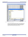
1
User Manual Data FLASH Converter Conversion tool for 78K0R, RL78, V850 and RH850 based Data FLASH memory image generation All information contained in these materials, including products and product specifications, represents information on the product at the time of publication and is subject to change by Renesas Electronics Corp. without notice. Please review the latest information published by Renesas Electronics Corp. through various means, including the Renesas Technology Corp. website (http://www.renesas.com). www.renesas.com R01UT0175ED0400, Rev. 4.00 May 11, 2015 Notice 1. All information included in this document is current as of the date this document is issued. Such information, however, is subject to change without any prior notice. Before purchasing or using any Renesas Electronics products listed herein, please confirm the latest product information with a Renesas Electronics sales office. Also, please pay regular and careful attention to additional and different information to be disclosed by Renesas Electronics such as that disclosed through our website. 2. Renesas Electronics does not assume any liability for infringement of patents, copyrights, or other intellectual property rights of third parties by or arising from the use of Renesas Electronics products or technical information described in this document. No license, express, implied or otherwise, is granted hereby under any patents, copyrights or other intellectual property rights of Renesas Electronics or others. 3. You should not alter, modify, copy, or otherwise misappropriate any Renesas Electronics product, whether in whole or in part. 4. Descriptions of circuits, software and other related information in this document are provided only to illustrate the operation of semiconductor products and application examples. You are fully responsible for the incorporation of these circuits, software, and information in the design of your equipment. Renesas Electronics assumes no responsibility for any losses incurred by you or third parties arising from the use of these circuits, software, or information. 5. When exporting the products or technology described in this document, you should comply with the applicable export control laws and regulations and follow the procedures required by such laws and regulations. You should not use Renesas Electronics products or the technology described in this document for any purpose relating to military applications or use by the military, including but not limited to the development of weapons of mass destruction. Renesas Electronics products and technology may not be used for or incorporated into any products or systems whose manufacture, use, or sale is prohibited under any applicable domestic or foreign laws or regulations. 6. Renesas Electronics has used reasonable care in preparing the information included in this document, but Renesas Electronics does not warrant that such information is error free. Renesas Electronics assumes no liability whatsoever for any damages incurred by you resulting from errors in or omissions from the information included herein. 7. Renesas Electronics products are classified according to the following three quality grades: “Standard”, “High Quality”, and “Specific”. The recommended applications for each Renesas Electronics product depends on the product’s quality grade, as indicated below. You must check the quality grade of each Renesas Electronics product before using it in a particular application. You may not use any Renesas Electronics product for any application categorized as “Specific” without the prior written consent of Renesas Electronics. Further, you may not use any Renesas Electronics product for any application for which it is not intended without the prior written consent of Renesas Electronics. Renesas Electronics shall not be in any way liable for any damages or losses incurred by you or third parties arising from the use of any Renesas Electronics product for an application categorized as “Specific” or for which the product is not intended where you have failed to obtain the prior written consent of Renesas Electronics. R01UT0175ED0400 Rev. 4.00 User Manual 2 8. The quality grade of each Renesas Electronics product is “Standard” unless otherwise expressly specified in a Renesas Electronics data sheets or data books, etc. “Standard”: Computers; office equipment; communications equipment; test and measurement equipment; audio and visual equipment; home electronic appliances; machine tools; personal electronic equipment; and industrial robots. “High Quality”: Transportation equipment (automobiles, trains, ships, etc.); traffic control systems; anti-disaster systems; anti- crime systems; safety equipment; and medical equipment not specifically designed for life support. “Specific”: Aircraft; aerospace equipment; submersible repeaters; nuclear reactor control systems;medical equipment or systems for life support (e.g. artificial life support devices or systems), surgical implantations, or healthcare intervention (e.g. excision, etc.), and any other applications or purposes that pose a direct threat to human life. 9. You should use the Renesas Electronics products described in this document within the range specified by Renesas Electronics, especially with respect to the maximum rating, operating supply voltage range, movement power voltage range, heat radiation characteristics, installation and other product characteristics. Renesas Electronics shall have no liability for malfunctions or damages arising out of the use of Renesas Electronics products beyond such specified ranges. 10. Although Renesas Electronics endeavors to improve the quality and reliability of its products, semiconductor products have specific characteristics such as the occurrence of failure at a certain rate and malfunctions under certain use conditions. Further, Renesas Electronics products are not subject to radiation resistance design. Please be sure to implement safety measures to guard them against the possibility of physical injury, and injury or damage caused by fire in the event of the failure of a Renesas Electronics product, such as safety design for hardware and software including but not limited to redundancy, fire control and malfunction prevention, appropriate treatment for aging degradation or any other appropriate measures. Because the evaluation of microcomputer software alone is very difficult, please evaluate the safety of the final products or system manufactured by you. 11. Please contact a Renesas Electronics sales office for details as to environmental matters such as the environmental compatibility of each Renesas Electronics product. Please use Renesas Electronics products in compliance with all applicable laws and regulations that regulate the inclusion or use of controlled substances, including without limitation, the EU RoHS Directive. Renesas Electronics assumes no liability for damages or losses occurring as a result of your noncompliance with applicable laws and regulations. 12. This document may not be reproduced or duplicated, in any form, in whole or in part, without prior written consent of Renesas Electronics. 13. Please contact a Renesas Electronics sales office if you have any questions regarding the information contained in this document or Renesas Electronics products, or if you have any other inquiries. (Note 1) “Renesas Electronics” as used in this document means Renesas Electronics Corporation and also includes its majority- owned subsidiaries. (Note 2) “Renesas Electronics product(s)” means any product developed or manufactured by or for Renesas Electronics. R01UT0175ED0400 Rev. 4.00 User Manual 3 Regional Information Some information contained in this document may vary from country to country. Before using any Renesas Electronics product in your application, please contact the Renesas Electronics office in your country to obtain a list of authorized representatives and distributors. They will verify: Device availability Ordering information Product release schedule Availability of related technical literature Development environment specifications (for example, specifications for third-party tools and components, host computers, power plugs, AC supply voltages, and so forth) Network requirements In addition, trademarks, registered trademarks, export restrictions, and other legal issues may also vary from country to country. Visit http://www.renesas.com to get in contact with your regional representatives and distributors. R01UT0175ED0400 Rev. 4.00 User Manual 4 Contents Chapter 1 1.1 1.2 1.3 Abbreviations................................................................................................... 6 Main features of Data FLASH Converter........................................................ 7 Trademarks ...................................................................................................... 8 Chapter 2 2.1 2.2 2.3 Introduction ......................................................................... 6 Input files / formats ............................................................. 9 Input file combinations ................................................................................... 9 Program Code for Data FLASH or Code FLASH ........................................... 9 EEPROM emulation data ................................................................................. 9 2.3.1 2.3.2 2.3.3 2.3.4 2.3.5 2.3.6 EEPROM EEPROM EEPROM EEPROM EEPROM EEPROM XML file format for V850 EEElib (previous Type) ........................................10 XML file format for V850 EEL (Type T05)......................................................12 XML file format for 78K0R EEL (Type T03) and RL78 EEL (Type T01) ......14 XML file format for V850 EEL (Type T06)......................................................16 XML file format for RL78 Tiny EEL (Type T02) .............................................18 XML file format for RH850 EEL (Type T01) ...................................................20 Chapter 3 Output file / formats .......................................................... 22 Chapter 4 Software Installation ......................................................... 23 Chapter 5 Data FLASH Converter GUI............................................... 27 5.1 5.2 Toolbar 28 The Menu 29 5.2.1 5.3 Process window ............................................................................................ 47 Chapter 6 6.1 6.2 Command line interface .................................................... 48 Command line options .................................................................................. 49 Combination of command line options ....................................................... 50 6.2.1 6.2.2 6.3 File menu ..........................................................................................................................29 Generation of merged Data FLASH / Code FLASH file ................................................51 Generation of Data FLASH file .......................................................................................52 Return Codes ................................................................................................. 60 Chapter 7 Error Messages ................................................................. 61 R01UT0175ED0400 Rev. 4.00 User Manual 5 Data FLASH Converter Introduction Chapter 1 Introduction The Data FLASH Converter is a windows based tool that generates a Data FLASH memory image from EEPROM emulation data and/or from a program code file that is mapped to the Data FLASH area of a Renesas microcontroller. Additionally the Data FLASH Converter is able to generate a merged output file containing EEPROM emulation data, user data (e.g. program code and constant data) for Data FLASH and for Code FLASH. This output file can be read by the standard Renesas FLASH programmer PG-FP5 and can be used for FLASH programming of a Renesas device containing Code FLASH and Data FLASH. Apart from the FLASH programmer support, the Data FLASH Converter can generate a data flash memory image that can be read by the standard debugger tool chain. This makes it possible to pre-initialize the Data FLASH memory also during the debugging phase. Depending on the device series, the flash implementation differs for various flash technologies; consequently, also the features of the flash are different. For example, ID tag is supported only for some device series, erase and write width differs etc. Please check carefully, which EEL is the right one for your device and which features are supported. 1.1 Abbreviations Abbreviations Description EEL EEPROM Emulation Library FAL FLASH Access Library (FLASH access layer) FDL FLASH Data Library (Data FLASH access layer) FSL FLASH Self-programming Library (accessing code FLASH) FW Firmware FCB FLASH Control Block: Hardware part of the device, which controls the flash macros(s). Depending on the device series, FCU may be used instead. ID tag An extension of a flash word, which allows to identify special data within the flash. An ID tag is supported only in Data Flash, and only for some Renesas device families. XML eXtensible Markup Language Table 1 Abbreviations R01UT0175ED0400 Rev. 4.00 User Manual 6 Data FLASH Converter Introduction 1.2 Main features of Data FLASH Converter Generates a initial Data FLASH memory image based on EEPROM emulation data represented by an XML file. Following EEPROM emulation library types for 78K0R, RL78 and V850 devices are currently supported. Refer to Renesas download pages to find out which EEL is the correct one for the device you are using. o V850 EELib: V850E/ES devices in MF2 or UX4 FLASH Technology in combination with the V850 EEPROM emulation library EEElib (previous Type). Example: V850ES/FX3, V850E/DX3. o V850 EEL T05: V850E2 devices in UX6 FLASH Technology in combination with the V850 EEPROM emulation library EEL (Type T05). Example: V850E2/FX4, V850E2/DX4, V850E2/PX4. o V850 EEL T06: V850E2 devices in RC03F FLASH Technology In combination with the V850 EEPROM emulation library EEL (Type T06). Example: V850E2/FX4-L, V850E2/PX4-L. o 78K0R EEL T03: 78K0R devices in MF2 FLASH Technology in combination with the 78K0R EEPROM emulation library EEL (Type T03). Example: 78K0R/FX3. o RL78 EEL T01: RL78 devices in MF3 FLASH Technology in combination with the RL78 EEPROM emulation library EEL (Type T01). Example: RL78/G1x, RL78/D1x o RL78 Tiny EEL T02: RL78 devices in MF3 FLASH Technology in combination with the RL78 Tiny EEPROM emulation library, Tiny EEL (Type T02). Example: RL78/G1x, RL78/D1x o RH850 EEL T01: RH850 devices in RV40 FLASH Technology in combination with the RH850 EEPROM emulation library EEL (Type T01). Example: RH850/F1x Merges EEPROM emulation data and program data (user data) into one Data FLASH memory image. Generates a Data FLASH memory image including ID-tag information (if applicable) from a program file mapped to the Data FLASH area. Supported input file formats are Intel-hex and Motorola S-record. For Intel-hex the extended linear address record and extended segment address record formats are supported. With regard to the Motorola-S record type, the S2 and S3 record formats are supported for program code mapped to the Data FLASH memory. Merges EEPROM emulation data and program data into one Data FLASH memory image. R01UT0175ED0400 Rev. 4.00 User Manual 7 Data FLASH Converter Introduction Merges Code FLASH programs and Data FLASH memory images into one output file. Generates two output files for FLASH programming and debugging purpose. Supports two output file formats: Intel-hex and Motorola-S record. A graphical user interface is provided as well as a command line interface for batch mode support or automatic output file generation. For V850 EEL library types T05 and T06, RH850 EEL library type T01 generates two header files. One is for the EEPROM Emulation Library of Renesas V850 device, another one is for the Data FLASH Access Library of Renesas V850 device. For 78K0R, RL78 and RL78 Tiny EEL library types, generates two header files and two source files. They are source/header files for the EEPROM Emulation Library of Renesas 78K0R/RL78 device, and source/header files for the Data FLASH Access Library of Renesas 78K0R/RL78 device. 1.3 Trademarks Microsoft and Windows are registered trademarks of Microsoft Corporation. All other product names are trademarks or registered trademarks of their respective owners. R01UT0175ED0400 Rev. 4.00 User Manual 8 Data FLASH Converter Input files / formats Chapter 2 Input files / formats 2.1 Input file combinations The Data FLASH Converter is able to handle the following combination of input files, for the generation of a single Data FLASH memory image or the generation of a merged Code FLASH / Data FLASH file. Supported combinations of input files Supported file formats 1 CodeFLASH program file + DataFLASH program file + EEPROM file HEX, SREC, XML 2 CodeFLASH program file + DataFLASH program file HEX, SREC 3 CodeFLASH program file + EEPROM file HEX, SREC, XML 4 DataFLASH program file + EEPROM file HEX, SREC, XML 5 DataFLASH program file HEX, SREC 6 EEPROM file XML Table 2 Supported combinations of input files 2.2 Program Code for Data FLASH or Code FLASH The program code has to be available in an Intel-hex or Motorola-S record format. For Intel-hex the extended linear address record and extended segment address record formats are supported. With regard to the Motorola-S record type, the S2 and S3 record formats are supported for program code mapped to the Data FLASH memory. For program files mapped to the Code FLASH the S1, S2 and S3 record formats are supported. The term ‘Program File’ in combination with Data Flash may mean either program code (not supported for all device series) and / or any constant data. 2.3 EEPROM emulation data To specify the EEPROM emulation data, the Data FLASH converter supports the standard XML file format (eXtensible Markup Language) as input format. Please also consult the manual of the EEPROM Emulation library that you are using for further details about the XML tags and their meaning. R01UT0175ED0400 Rev. 4.00 User Manual 9 Data FLASH Converter Input files / formats 2.3.1 EEPROM XML file format for V850 EEElib (previous Type) The XML input format and the corresponding XML tags for V850E/ES devices in UX4 and MF2 FLASH Technology in combination with the V850 EEPROM emulation library V850 EEElib (previous Type) is shown below. <?xml version="1.0"?> <DataFlash> <AdministrativeSection> <SectionSize>0x0800</SectionSize> <Offset>0x0000</Offset> </AdministrativeSection> <Record> <ID>0x80</ID> <Length>4</Length> <Data>0x20,0x30,0x40,0x50</Data> </Record> <Record> <ID>0x81</ID> <Length>8</Length> <Data> 0x20,0x30,0x31,0x32, 0x40,0x40,0x41,0x42 </Data> </Record> </DataFlash> Figure 1 EEPROM emulation data, XML file format for V850 EEElib (previous Type) The predefined XML tags are: DataFlash Defining the start of the definition file. AdminstrativeSection This section is describing the physical parameters that are needed for the file generation. SectionSize Size of one section that is used for the EEPROM emulation, e.g. 0x800 (2 kByte), 0x1000 (4 kByte), 0x2000 (8 kByte), 0x4000 (16 kByte)… Offset The offset where the section starts in the Data FLASH. It is always related to the start address of the Data FLASH. The offset can have a size of 2 kByte * n. Record Defining the start of a ID-L record. ID Identifier for the data record (16bit). Format is fixed to four digits in hex. Length Length definition of the data record (16bit). Format is fixed to four digits in hex. The minimum data length is equal to four bytes. The length can be specified in 4 Byte *n steps. Data Any hexadecimal or decimal value. The line length is not fixed. R01UT0175ED0400 Rev. 4.00 User Manual 10 Data FLASH Converter Input files / formats Comments have to be added as specified in XML definition starting with ‘<!-- ’ and ending with ‘ -->’. The values defining the ID, length or data information must have the following ‘C’ like notation: o Leading ‘0x’ denotes a hex value. o Leading zeros within a hex value are interpreted by the Data FLASH Converter and do also determine the width of a Data value. Example: 0x00 0x0012 0x00000023 o → → → data width = 1 Byte data width = 2 Byte data width = 4 Byte All other notation is interpreted as decimal value Values have to be separated by either space ‘ ‘ or comma ‘,’. R01UT0175ED0400 Rev. 4.00 User Manual 11 Data FLASH Converter Input files / formats 2.3.2 EEPROM XML file format for V850 EEL (Type T05) The XML input format and the corresponding XML tags for V850E2 devices in UX6 FLASH Technology in combination with the V850 EEPROM emulation library EEL (Type T05) is shown below. <?xml version="1.0"?> <DataFlash> <AdministrativeSection> <FAL_CONFIG_DATAFLASH_SIZE>16</FAL_CONFIG_DATAFLASH_SIZE> <FAL_CONFIG_BLOCK_SIZE>0x800</FAL_CONFIG_BLOCK_SIZE> <EEL_CONFIG_BLOCK_START>2</EEL_CONFIG_BLOCK_START> <EEL_CONFIG_BLOCK_CNT>6</EEL_CONFIG_BLOCK_CNT> <EEL_CONFIG_DF_BASE_ADDRESS>0x2000000</EEL_CONFIG_DF_BASE_ADDRESS> <EEL_CONFIG_BLOCK_CNT_REFRESH_THRESHOLD>0x02 </EEL_CONFIG_BLOCK_CNT_REFRESH_THRESHOLD> <EEL_CONFIG_ERASE_SUSPEND_THRESHOLD>10 </EEL_CONFIG_ERASE_SUSPEND_THRESHOLD> </AdministrativeSection> <Record> <ID>0x80</ID> <IDName>Name1</IDName> <Length>2</Length> <Data>0x20,0x30</Data> </Record> <Record> <ID>0x10</ID> <IDName>Name2</IDName> <Length>5</Length> <Data>0x20,0x30,0x31,0x32,0x33</Data> </Record> </DataFlash> Figure 2 EEPROM emulation data, XML file format for V580 EEL (Type 05) R01UT0175ED0400 Rev. 4.00 User Manual 12 Data FLASH Converter Input files / formats The predefined XML tags are: DataFlash Defining the start of the definition file. AdminstrativeSection This section is describing the physical parameters that are needed for the file generation. FAL_CONFIG_DATAFLASH_SIZE Number of Data FLASH blocks, accessible by the FAL. Typical number of available Data FLASH blocks. FAL_CONFIG_BLOCK_SIZE Data FLASH block size in bytes. EEL_CONFIG_BLOCK_START 1st block of the EEL pool. EEL_CONFIG_BLOCK_CNT Number of blocks for the EEL pool. EEL_CONFIG_DF_BASE_ADDRESS Data FLASH base address. EEL_CONFIG_BLOCK_CNT_REFRESH_THRESHOLD Threshold for minimum number of prepared blocks. EEL_CONFIG_ERASE_SUSPEND_THRESHOLD Record ID IDName Length Data Threshold for erase suspend counter. Exceeding this results in warning. Defining the start of a ID-L record. Identifier for the data record (16bit). Format is fixed to four digits in hex. Defining the name off the record. Length definition of the data record. Any hexadecimal or decimal value. The line length is not fixed. Comments have to be added as specified in XML definition starting with ‘<!-- ’ and ending with ‘ -->’. The values defining the ID, length or data information must have the following ‘C’ like notation: o Leading ‘0x’ denotes a hex value. o Leading zeros within a hex value are interpreted by the Data FLASH Converter and do also determine the width of a Data value. Example: 0x00 0x0012 0x00000023 o → → → data width = 1 Byte data width = 2 Byte data width = 4 Byte All other notation is interpreted as decimal value Values have to be separated by either space ‘ ‘ or comma ‘,’. R01UT0175ED0400 Rev. 4.00 User Manual 13 Data FLASH Converter Input files / formats 2.3.3 EEPROM XML file format for 78K0R EEL (Type T03) and RL78 EEL (Type T01) The XML input format and the corresponding XML tags for: - 78K0R devices in MF2 FLASH Technology in combination with the 78K0R EEPROM emulation library 78K0R EEL (Type T03) - RL78 devices in MF3 FLASH Technology in combination with the RL78K EEPROM emulation library RL78 EEL (Type T01) is shown below. <?xml version="1.0"?> <DataFlash> <AdministrativeSection> <FAL_CONFIG_DATAFLASH_SIZE>8</FAL_CONFIG_DATAFLASH_SIZE> <FAL_CONFIG_BLOCK_SIZE>0x800</FAL_CONFIG_BLOCK_SIZE> <EEL_CONFIG_BLOCK_CNT>4</EEL_CONFIG_BLOCK_CNT> <EEL_CONFIG_BLOCK_CNT_REFRESH_THRESHOLD>2 </EEL_CONFIG_BLOCK_CNT_REFRESH_THRESHOLD> </AdministrativeSection> <Record> <ID>0x80</ID> <IDName>Name1</IDName> <Length>2</Length> <Data>0x20,0x30</Data> </Record> <Record> <ID>0x10</ID> <IDName>Name2</IDName> <Length>5</Length> <Data>0x20,0x30,0x31,0x32,0x33</Data> </Record> </DataFlash> Figure 3 EEPROM emulation data, XML file format for 78K0R EEL (Type T03) and RL78 EEL (Type T01) R01UT0175ED0400 Rev. 4.00 User Manual 14 Data FLASH Converter Input files / formats The predefined XML tags are: DataFlash Defining the start of the definition file. AdminstrativeSection This section is describing the physical parameters that are needed for the file generation. FAL_CONFIG_DATAFLASH_SIZE or FAL_CONFIG_POOL_SIZE Number of Data FLASH blocks, accessible by the FAL. Typical number of available Data FLASH blocks. FAL_CONFIG_BLOCK_SIZE Data FLASH block size in bytes (note: different values for 78K0R and RL78 EEL). EEL_CONFIG_BLOCK_START 1st block of the EEL pool. It is fixed to 0. This tag can be neglected. EEL_CONFIG_BLOCK_CNT Number of blocks for the EEL pool. Threshold for minimum number of prepared blocks. Defining the start of a ID-L record. Identifier for the data record (8bit). Format is fixed to two digits in hex. Defining the name off the record. Length definition of the data record. In the range of 1-FFh Any hexadecimal or decimal value. The line length is not fixed. The number of data in a record should not large as length information. EEL_CONFIG_BLOCK_CNT_REFRESH_THRESHOLD Record ID IDName Length Data Comments have to be added as specified in XML definition starting with ‘<!-- ’ and ending with ‘ -->’. The values defining the ID, length or data information must have the following ‘C’ like notation: o Leading ‘0x’ denotes a hex value. o Leading zeros within a hex value are interpreted by the Data FLASH Converter and do also determine the width of a Data value. Example: 0x00 0x0012 0x00000023 o → → → data width = 1 Byte data width = 2 Byte data width = 4 Byte All other notation is interpreted as decimal value Values have to be separated by either space ‘ ‘ or comma ‘,’. R01UT0175ED0400 Rev. 4.00 User Manual 15 Data FLASH Converter Input files / formats 2.3.4 EEPROM XML file format for V850 EEL (Type T06) The XML input format and the corresponding XML tags for V850E2 devices in RC03F FLASH Technology in combination with the V850 EEPROM emulation library EEL (Type T06) is shown below. <?xml version="1.0"?> <DataFlash> <AdministrativeSection> <FAL_CONFIG_DATAFLASH_SIZE>16</FAL_CONFIG_DATAFLASH_SIZE> <FAL_CONFIG_BLOCK_SIZE>0x800</FAL_CONFIG_BLOCK_SIZE> <EEL_CONFIG_BLOCK_START>2</EEL_CONFIG_BLOCK_START> <EEL_CONFIG_BLOCK_CNT>6</EEL_CONFIG_BLOCK_CNT> <EEL_CONFIG_DF_BASE_ADDRESS>0xFE000000</EEL_CONFIG_DF_BASE_ADDRESS> <EEL_CONFIG_BLOCK_CNT_REFRESH_THRESHOLD>0x03 </EEL_CONFIG_BLOCK_CNT_REFRESH_THRESHOLD> <EEL_CONFIG_ERASE_SUSPEND_THRESHOLD>10 </EEL_CONFIG_ERASE_SUSPEND_THRESHOLD> </AdministrativeSection> <Record> <ID>0x80</ID> <IDName>Name1</IDName> <Length>2</Length> <Data>0x20,0x30</Data> </Record> <Record> <ID>0x10</ID> <IDName>Name2</IDName> <Length>5</Length> <Data>0x20,0x30,0x31,0x32,0x33</Data> </Record> </DataFlash> Figure 4 EEPROM emulation data, XML file format for V850 EEL (Type T06) R01UT0175ED0400 Rev. 4.00 User Manual 16 Data FLASH Converter Input files / formats The predefined XML tags are: DataFlash Defining the start of the definition file. AdminstrativeSection This section is describing the physical parameters that are needed for the file generation. FAL_CONFIG_DATAFLASH_SIZE or FAL_CONFIG_POOL_SIZE Number of Data FLASH blocks, accessible by the FAL. Typical number of available Data FLASH blocks. FAL_CONFIG_BLOCK_SIZE Data FLASH block size in bytes. EEL_CONFIG_BLOCK_START 1st block of the EEL pool. EEL_CONFIG_BLOCK_CNT Number of blocks for the EEL pool. EEL_CONFIG_DF_BASE_ADDRESS Data FLASH base address. Fixed to 0xFE000000 EEL_CONFIG_BLOCK_CNT_REFRESH_THRESHOLD Threshold for minimum number of prepared blocks. Threshold for erase suspend counter. Exceeding this results in warning. Defining the start of a ID-L record. Identifier for the data record (16bit). Format is fixed to four digits in hex. Defining the name off the record. Length definition of the data record. The length should not larger then valid block space. Any hexadecimal or decimal value. The line length is not fixed. The number of data in a record should not large as length information. EEL_CONFIG_ERASE_SUSPEND_THRESHOLD Record ID IDName Length Data Comments have to be added as specified in XML definition starting with ‘<!-- ’ and ending with ‘ -->’. The values defining the ID, length or data information must have the following ‘C’ like notation: o Leading ‘0x’ denotes a hex value. o Leading zeros within a hex value are interpreted by the Data FLASH Converter and do also determine the width of a Data value. Example: 0x00 0x0012 0x00000023 o → → → data width = 1 Byte data width = 2 Byte data width = 4 Byte All other notation is interpreted as decimal value Values have to be separated by either space ‘ ‘ or comma ‘,’. R01UT0175ED0400 Rev. 4.00 User Manual 17 Data FLASH Converter Input files / formats 2.3.5 EEPROM XML file format for RL78 Tiny EEL (Type T02) The XML input format and the corresponding XML tags for: - RL78 devices in MF3 FLASH Technology in combination with the RL78 Tiny EEPROM emulation library (Type T02) is shown below: <?xml version="1.0"?> <DataFlash> <AdministrativeSection> <FAL_CONFIG_DATAFLASH_SIZE>16</FAL_CONFIG_DATAFLASH_SIZE> <FAL_CONFIG_BLOCK_SIZE>0x400</FAL_CONFIG_BLOCK_SIZE> <EEL_CONFIG_BLOCK_CNT>4</EEL_CONFIG_BLOCK_CNT> <TYPE_TINY>1</TYPE_TINY> <COMPILER>IAR</COMPILER> </AdministrativeSection> <Record> <ID>0x01</ID> <IDName>Name1</IDName> <Length>2</Length> <Data>0x20,0x30</Data> </Record> <Record> <ID>0x02</ID> <IDName>Name2</IDName> <Length>5</Length> <Data>0x20,0x30,0x31,0x32,0x33</Data> </Record> </DataFlash> Figure 5 EEPROM emulation data, XML file format for RL78 Tiny EEL (Type T02) R01UT0175ED0400 Rev. 4.00 User Manual 18 Data FLASH Converter Input files / formats The predefined XML tags are: DataFlash Defining the start of the definition file. AdminstrativeSection This section is describing the physical parameters that are needed for the file generation. FAL_CONFIG_DATAFLASH_SIZE or FAL_CONFIG_POOL_SIZE Number of Data FLASH blocks, accessible by the FAL. Typical number of available Data FLASH blocks. FAL_CONFIG_BLOCK_SIZE Data FLASH block size in bytes EEL_CONFIG_BLOCK_CNT Number of blocks for the EEL pool. TYPE_TINY For RL78 device, ”1” define for EEL type T02, “0” for Eel type T01. And the default type is T01. Define the compiler output format. “IAR” defines that the IAR compiler will be used, “REN” defines that Renesas compiler will be used. Default compiler is “IAR” Defining the start of a ID-L record. Identifier for the data record (8bit). Format is fixed to two digits in hex. Defining the name of the record. Length definition of the data record. In the range of 1-FFh Any hexadecimal or decimal value. The line length is not fixed. The number of data in a record should not be larger than the value for ‘Length’. COMPILER Record ID IDName Length Data Comments have to be added as specified in XML definition starting with ‘<!-- ’ and ending with ‘ -->’. The values defining the ID, length or data information must have the following ‘C’ like notation: o Leading ‘0x’ denotes a hex value. o Leading zeros within a hex value are interpreted by the Data FLASH Converter and do also determine the width of a Data value. Example: 0x00 0x0012 0x00000023 o → → → data width = 1 Byte data width = 2 Byte data width = 4 Byte All other notation is interpreted as decimal value Values have to be separated by either space ‘ ‘ or comma ‘,’. R01UT0175ED0400 Rev. 4.00 User Manual 19 Data FLASH Converter Input files / formats 2.3.6 EEPROM XML file format for RH850 EEL (Type T01) The XML input format and the corresponding XML tags for: - RH850 devices in RV40 FLASH Technology in combination with the RH850 EEPROM emulation library (Type T01) is shown below: <?xml version="1.0"?> <DataFlash> <AdministrativeSection> <FAL_CONFIG_DATAFLASH_SIZE>512</FAL_CONFIG_DATAFLASH_SIZE> <EEL_CONFIG_BLOCK_SIZE>0x800</FAL_CONFIG_BLOCK_SIZE> <EEL_CONFIG_BLOCK_START>2</EEL_CONFIG_BLOCK_START> <EEL_CONFIG_BLOCK_CNT>6</EEL_CONFIG_BLOCK_CNT> <EEL_CONFIG_DF_BASE_ADDRESS>0xFF200000</EEL_CONFIG_DF_BASE_ADDRESS> <EEL_CONFIG_BLOCK_CNT_REFRESH_THRESHOLD>0x02 </EEL_CONFIG_BLOCK_CNT_RE FRESH_THRESHOLD> <EEL_CONFIG_ERASE_SUSPEND_THRESHOLD>10 </EEL_CONFIG_ERASE_SUSPEND_THRESHOLD> <FDL_CPU_FREQUENCY_MHZ>70</FDL_CPU_FREQUENCY_MHZ> </AdministrativeSection> <Record> <ID>0x011</ID> <IDName>Name1</IDName> <Length>2</Length> <Data>0x20,0x30</Data> </Record> <Record> <ID>0x022</ID> <IDName>Name2</IDName> <Length>5</Length> <Data>0x20,0x30,0x31,0x32,0x33</Data> </Record> </DataFlash> Figure 6 EEPROM emulation data, XML file format for RH850 EEL (Type T01) R01UT0175ED0400 Rev. 4.00 User Manual 20 Data FLASH Converter Input files / formats The predefined XML tags are: DataFlash Defining the start of the definition file. AdminstrativeSection This section is describing the physical parameters that are needed for the file generation. FAL_CONFIG_DATAFLASH_SIZE or FAL_CONFIG_POOL_SIZE Number of Data FLASH blocks, accessible by the FAL. Typical number of available Data FLASH blocks. EEL_CONFIG_BLOCK_SIZE Virtual Data FLASH block size in bytes EEL_CONFIG_BLOCK_START Start virtual block number for the EEL pool. EEL_CONFIG_BLOCK_CNT Number of virtual blocks for the EEL pool. EEL_CONFIG_DF_BASE_ADDRESS Data FLASH base address which defined in ‘*.pr5’ parameter file. EEL_CONFIG_BLOCK_CNT_REFRESH_THRESHOLD Threshold for minimum number of prepared blocks. EEL_CONFIG_ERASE_SUSPEND_THRESHOLD Threshold for erase suspend counter. Exceeding this results in warning. FDL_CPU_FREQUENCY_MHZ Record ID Defining CPU frequency in MHz Defining the start of a ID-L record. Identifier for the data record (8bit). Format is fixed to two digits in hex. Defining the name of the record. Length definition of the data record. In the range of 1-FFh Any hexadecimal or decimal value. The line length is not fixed. The number of data in a record should not be larger than the value for ‘Length’. IDName Length Data Comments have to be added as specified in XML definition starting with ‘<!-- ’ and ending with ‘ -->’. The values defining the ID, length or data information must have the following ‘C’ like notation: o Leading ‘0x’ denotes a hex value. o Leading zeros within a hex value are interpreted by the Data FLASH Converter and do also determine the width of a Data value. Example: 0x00 0x0012 0x00000023 o → → → data width = 1 Byte data width = 2 Byte data width = 4 Byte All other notation is interpreted as decimal value Values have to be separated by either space ‘ ‘ or comma ‘,’. R01UT0175ED0400 Rev. 4.00 User Manual 21 Data FLASH Converter Output file / formats Chapter 3 Output file / formats The output format of the Data FLASH converter is always the same as the chosen input file format for program code mapped to the Data FLASH, as well as the program code mapped to the Code FLASH. In case a Data FLASH image should be created from EEPROM emulation data exclusively, the output format can be chosen between Intel-hex and Motorola-S record. R01UT0175ED0400 Rev. 4.00 User Manual 22 Data FLASH Converter Software Installation Chapter 4 Software Installation The Data FLASH Converter requires Windows 2000, Windows XP, Windows Vista or Windows 7 operating system installed on your personal computer. To start the installation, please run the “setup.exe” installation program. During initialization phase of the setup program a progress bar is shown. Figure 6 Install preparation After the setup program has finished initialization a welcome screen appears. Click the Next button to continue the installation. Figure 7 Welcome screen R01UT0175ED0400 Rev. 4.00 User Manual 23 Data FLASH Converter Software Installation In the next step of installation, the License Agreement window appears. Please read the Software Program License Agreement carefully. To continue the installation accept the License agreement and click the Next button. If you not accepted the license agreement the installation procedure exits. Figure 8 License Agreement window The Destination Folder window appears. You might exit the installation by clicking the Cancel button. You can click the Change button to be able to change the installation destination path. Press the Next button to proceed with the installation. Figure 9 Choose Destination Folder window R01UT0175ED0400 Rev. 4.00 User Manual 24 Data FLASH Converter Software Installation After everything has been setup for installation, press the Install button to start the copy process and to finalize the installation. Figure 10 Ready to install window On the installation progress window you can follow the installation. You can always abort the installation by pressing the Cancel button. Figure 11 Installation progress window R01UT0175ED0400 Rev. 4.00 User Manual 25 Data FLASH Converter Software Installation When the installation is complete, the following message window appears. Figure 12 Installation completion window The program has been installed successfully and an entry has been made into the program menu to start the Data FLASH Converter software. The installation process is complete now and the setup utility has installed a new program folder which holds the Data FLASH Converter GUI Software and a Data FLASH Converter uninstall icon which allows you to remove the Data FLASH Converter software from your personal computer. Figure 13 Program folder after installation R01UT0175ED0400 Rev. 4.00 User Manual 26 Data FLASH Converter Data FLASH Converter GUI Chapter 5 Data FLASH Converter GUI The graphical user interface of the Data FLASH Converter allows an easy and intuitive configuration and generation of Data FLASH memory images. When starting the Data FLASH Converter GUI a screen similar to the following one will appear. Some commands and functions may be unavailable when the GUI is started for the first time, depending on the specified device parameter file, Data FLASH area definition or the loaded program files or loaded EEPROM file. <1> Menu bar <2> Toolbar <6> Hint bar <3> Config window <4> Address map window <5> process window Figure 14 Data FLASH Converter main window R01UT0175ED0400 Rev. 4.00 User Manual 27 Data FLASH Converter Data FLASH Converter GUI The main window consists of the following areas. Name Displayed items <1> Menu bar Menu items executable by the Data FLASH Converter <2> Toolbar Frequently used commands, as buttons <3> Config window Configuration settings <4> Address map window Address map information for Code FLASH and Data FLASH memory images <5> Process window Controls to start conversion, merging or reset of all configuration settings <6> Hint bar Hints for commands and toolbar Table 3 Main window composition 5.1 Toolbar The toolbar contains buttons to configure the Data FLASH Converter and to start all key functions quickly. The following buttons and corresponding functions are offered by the Data FLASH converter. Open Device Parameter File Setup Data FLASH area Open EEPROM emulation data Open program file for Data FLASH Open program file for Code FLASH Generate merged Data / Code FLASH file Generate Data FLASH file Open HEX editor / viewer Figure 15 Toobar buttons R01UT0175ED0400 Rev. 4.00 User Manual 28 Data FLASH Converter Data FLASH Converter GUI 5.2 The Menu Analogue to the Toolbar the main menu of the Data FLASH Converter allows the configuration and execution of all converter functions. 5.2.1 File menu The File menu allows starting a HEX file editor/viewer, setting the Data FLASH area, loading a program file for Data FLASH or respectively Code FLASH and loading an EEPROM emulation file in various formats. Additional the generation of a Data FLASH file or the output of a merged Code FLASH / Data FLASH file can be controlled via the file menu. (1) (2) (3) (4) (5) (6) (7) (8) (9) Figure 16 File menu (1) Hex editor / viewer The HEX Editor menu allows to edit / display a program file in Intel HEX file format or MotorolaS-Record format. A HEX editor window opens and in a file open dialog the file to be edited can be specified. Additional to this a generated Data FLASH file or a merged Code/Data FLASH file can be displayed or edited by the HEX editor. To use the HEX editor the Data FLASH area must be specified first. The display of the Data FLASH contents and ID-tag information is always based on the setting of the Data FLASH area. R01UT0175ED0400 Rev. 4.00 User Manual 29 Data FLASH Converter Data FLASH Converter GUI Figure 17 Hex Editor, open file dialog HEX Files (*.HEX), SREC Files (*.REC) or All files (*.*) may be selected from the Files of types list box. After selecting a file to be opened, the file selected in the HEX Editor main window is loaded. At this time, whether the file is of the Intel HEX format or Motorola-S record format is automatically recognized. When loading is finished, the HEX Editor main window is opened. R01UT0175ED0400 Rev. 4.00 User Manual 30 Data FLASH Converter Data FLASH Converter GUI Address area Data area ASCII area ID Tag area Figure 18 Hex Editor, main window The displayed file contents can be modified by placing the cursor in the data display area in the HEX Editor main window. Data input via the keyboard is accepted for all shown memory locations. The ID Tag area is an area used for target devices supporting Data FLASH. It is available only for the address space of the Data FLASH area specified within the Data FLASH Converter. Input 0 or 1 for the ID Tag area. If 0 is input, then 00000000h will be set, and if 1 is input, FFFFFFFFh will be used as ID Tag within the HEX file. For details on Data FLASH and ID Tags, refer to the user’s manual of the target device. The HEX Editor only accepts hexadecimal data, i.e., numbers 0 to 9 and letters A to F. All other data will be rejected. R01UT0175ED0400 Rev. 4.00 User Manual 31 Data FLASH Converter Data FLASH Converter GUI The ASCII representation, if any, is shown in the ASCII display area. This area is for reference only, so no data can be input. Use the scroll bar to move another address range into the visible area of the HEX Editor. The address space that can be viewed in the HEX Editor window is up to 4 MB + 64 KB (Data FLASH space). The following keys can be input using the keyboard. Key Function 0-9, A-F Data input → Move cursor in right direction ← Move cursor in left direction ↑ Move cursor in up direction ↓ Move cursor in down direction Tab Tab Move cursor to next input field (address + 1) Table 4 Hex Editor, navigation and input keys If any changes have been made to the file, [Save] and [Save As] in the [File] menu in the HEX Editor main window becomes available for saving the modified data. Figure 19 Hex Editor, Save as dialog R01UT0175ED0400 Rev. 4.00 User Manual 32 Data FLASH Converter Data FLASH Converter GUI Besides the file name and folder location, a start address and an end address for the new file can be selected in the [Save As] dialog box. The original start address and end address are displayed by default. Select the file radio button for the format in which to save the data. Select the same format as that of the loaded file. The relationship between the HEX Editor and saved File for the Data FLASH can bee seen in the figure below: Figure 20 Hex Editor, format of saved Data FLASH file (2) Open Device Parameter File The Open Device Parameter File menu allows to setup the corresponding PGFP5 FLASH programmer device parameter file. Before further settings and operations can be made within the Data FLASH Converter GUI the corresponding “*.pr5” file has to be specified. Figure 21 Open Device Parameter File R01UT0175ED0400 Rev. 4.00 User Manual 33 Data FLASH Converter Data FLASH Converter GUI V850 EEElib The start address of the Data FLASH area of these V850 devices, based on MF2 (previous type): or UX4 FLASH Technology (e.g. V850E/Xx3, V850ES/Xx3), is not fixed. It can be changed device dependent to different chip select areas. Within the Setup Data FLASH dialog, the start address of the Data FLASH must be specified. The entered start address should be equal to the physical start address of the Data FLASH area of the corresponding V850 device. The size of the Data FLASH can be specified by the pull-down menu. Supported sizes are 32 Kbyte and 64 Kbyte. V850 EEL The start address, end address and size of the Data FLASH area of these V850 (Type 05): devices, based on UX6 FLASH Technology (V850E2/Xx4), is defined by the device parameter file. According to this, the Data FLASH area parameters can not be changed within the “Set Data FLASH area” menu. V850 EEL The start address, end address and size of the Data FLASH area of these V850 (Type T06): devices, based on RC03F FLASH Technology (V850E2/Xx4-L), is defined by the device parameter file. According to this, the Data FLASH area parameters can not be changed within the “Set Data FLASH area” menu. 78K0R EEL The start address of the Data FLASH area of these 78K0R devices, based on (Type T03): MF2 Technology (e.g. 78K0R/FX3), is fixed. The size of the Data FLASH area of these devices is defined by the device parameter file. According to this, the Data FLASH area parameters can not be changed within the “Set Data FLASH area” menu. RL78 EEL (Type T01): RL78 Tiny EEL (Type T02): The start address, end address and size of the Data FLASH area of these RL78 devices, based on MF3 FLASH Technology , is defined by the device parameter file. According to this, the Data FLASH area parameters can not be changed within the “Set Data FLASH area” menu. R01UT0175ED0400 Rev. 4.00 User Manual 34 Data FLASH Converter (3) Data FLASH Converter GUI Set Data FLASH area The Set Data FLASH area menu allows to setup the start address and the size of the Data FLASH area. This menu is only available for devices using the EEElib (previous type). For all other devices, the Data FLASH area is fixed to special address and can not be changed. The actual values are displayed in the Data FLASH area box. By selecting this menu item the following dialog window appears and offers the possibility to specify the Data FLASH mapping. Figure 22 Set Data FLASH start address Within the Setup Data FLASH dialog the start address of the Data FLASH must be specified. Only hexadecimal input values are allowed. The entered start address should be equal to the physical start address of the Data FLASH area of the corresponding devices. The size of the Data FLASH can be specified by the pull-down menu. Supported sizes are 32 Kbyte and 64 Kbyte. Figure 23 Set Data FLASH size R01UT0175ED0400 Rev. 4.00 User Manual 35 Data FLASH Converter Data FLASH Converter GUI By closing the dialog pressing the <OK> button, the specified memory area is displayed in the Data FLASH area box of the main window. Figure 24 Config window, Data FLASH area box Additional to the file menu and toolbox button the Data FLASH area can be specified by pressing the <Set> button within the Data FLASH area box. R01UT0175ED0400 Rev. 4.00 User Manual 36 Data FLASH Converter (4) Data FLASH Converter GUI Open Data FLASH EEPROM file The Open Data FLASH EEPROM file menu allows selecting and loading an EEPROM emulation data file by the Data FLASH Converter. After downloading the EEPROM emulation data the corresponding memory area within the Data FLASH is shown in the address map window. Figure 25 Open Data FLASH EEPROM file dialog The most recently used directory a file has been loaded from will be offered in this file open menu. EEPROM emulation data can be loaded in the XML file format. After EEPROM emulation data is loaded the corresponding file and file format is displayed in the Config window of the Data FLASH converter. Figure 26 Config window, Data FLASH EEPROM file box R01UT0175ED0400 Rev. 4.00 User Manual 37 Data FLASH Converter Data FLASH Converter GUI Additional to the file menu and toolbox button the EEPROM emulation data can be loaded by pressing the <Read> button within the Config window of the Data FLASH Converter. The<Clear> button offers the possibility to delete a current selected file. To get information about the needed Data FLASH memory for the EEPROM emulation data, the mapping is shown in the address map window of the Data FLASH converter. Figure 27 Address map window, Data FLASH memory box (1) R01UT0175ED0400 Rev. 4.00 User Manual 38 Data FLASH Converter (5) Data FLASH Converter GUI Open Data FLASH program file The Open Data FLASH program file menu allows selecting and loading a program file that is linked to be executed from the Data FLASH memory. After downloading the program file the corresponding memory area where the program is placed within the Data FLASH is shown in the address map window. Figure 28 Open Data FLASH program file dialog The program code has to be available in an Intel-hex or Motorola-S record format. For Intel-hex the extended linear address record and extended segment address record formats are supported. With regard to the Motorola-S record type, the S2 and S3 record formats are supported for program code mapped to the Data FLASH memory. After the program code is loaded the corresponding file and file format is displayed in the Config window of the Data FLASH converter. Figure 29 Config window, Data FLASH program file box Additional to the file menu and toolbox button the program file can be loaded by pressing the <Read> button within the Config window of the Data FLASH Converter. The<Clear> button offers the possibility to delete a current selected file. R01UT0175ED0400 Rev. 4.00 User Manual 39 Data FLASH Converter Data FLASH Converter GUI To get information about the address map of the program file, the mapping is shown in the address map window of the Data FLASH converter. Figure 30 Address map window, Data FLASH memory box (2) R01UT0175ED0400 Rev. 4.00 User Manual 40 Data FLASH Converter (6) Data FLASH Converter GUI Open Code FLASH program file The Open Code FLASH program file menu allows selecting and loading a program file that is linked to be executed from the Code FLASH memory. After downloading the program file the corresponding memory area where the program is placed within the Code FLASH is shown in the address map window. Figure 31 Open Code FLASH program file dialog The program code has to be available in an Intel-hex or Motorola-S record format. For Intel-hex the extended linear address record and extended segment address record formats are supported. With regard to the Motorola-S record type, the S1, S2 and S3 record formats are supported for program files mapped to the Code FLASH. After the program code is loaded the corresponding file and file format is displayed in the Config window of the Data FLASH converter. Figure 32 Config window, Code FLASH Program file box Additional to the file menu and toolbox button the program file can be loaded by pressing the <Read> button within the Config window of the Data FLASH Converter. The<Clear> button offers the possibility to delete a current selected file. R01UT0175ED0400 Rev. 4.00 User Manual 41 Data FLASH Converter Data FLASH Converter GUI To get information about the address map of the program file, the mapping is shown in the address map window of the Data FLASH converter. Figure 33 Address map window, Code FLASH memory box R01UT0175ED0400 Rev. 4.00 User Manual 42 Data FLASH Converter (7) Data FLASH Converter GUI Generate merged Data FLASH / Code FLASH file The Generate merged Data FLASH / Code FLASH file menu allows to generate a merged output file including Data FLASH and Code FLASH information. The file format of the generated file depends on the format of the loaded program file for the Data FLASH respectively Code FLASH. By executing this command a file save dialog opens and offers the possible to specify the name and location of the output file to be generated. Figure 34 Save merged Data FLASH / Code FLASH file dialog This merged output file can be read by the standard Renesas FLASH programmer PG-FP5 and can be used for FLASH programming of a Renesas device containing Code FLASH and Data FLASH. Note for devices using V850 EEELib or 78K0R EEL: The Renesas FLASH programmer uses the serial programming mode for programming the Data FLASH memory. Within this mode, the Data FLASH memory is accessed for reading and writing via the FLASH Control hardware unit (FCB, FCU) of the corresponding device. By writing or reading via the Flash Control hardware unit, the start address of the Data FLASH memory is always 0x0400000 (V850E1/ES) or 0xF1000 (78K0R) regardless of the used device. This address differs to the physical mapping of Data FLASH within normal mode, where the Data FLASH memory is accessed via the instruction fetch or data bus of the device. Note: A merged Data FLASH / Code FLASH file can not be used for debugging purpose. R01UT0175ED0400 Rev. 4.00 User Manual 43 Data FLASH Converter (8) Data FLASH Converter GUI Generate Data FLASH file The Generate Data FLASH file menu allows to generate a output file including Data FLASH information only. In case EEPROM emulation data and program code for Data FLASH are specified together a single output file is generate representing the complete Data FLASH memory image. Within this case, the file format of the generated output file depends on the format of the loaded Data FLASH program file. By exclusively converting EEPROM emulation data the format of the output file can be chosen between Intel-hex and MotorolaS record. By executing the Generate Data FLASH file command a file save dialog opens and offers the possible to specify the name and location of the output file to be generated. Figure 35 Save Data FLASH file dialog R01UT0175ED0400 Rev. 4.00 User Manual 44 Data FLASH Converter Data FLASH Converter GUI V850 EEElib: By generating a Data FLASH file two separate output files are generated, one for FLASH programming and the other one for debugging purpose. The file for debugging purpose includes the marking “.dbg“ within the file name and is mapped to the Data FLASH memory area specified by the user. The file for FLASH programming purpose has no additional marking within its name and is mapped to address 0x0400000. Please refer also to Figure 38. Background: The Renesas FLASH programmer uses the serial programming mode for programming the Data FLASH memory of a V850E1/ES device. Within this mode the Data FLASH memory is accessed for reading and writing via the FLASH Control Block macro (FCB) of the corresponding V850E1/ES device. By writing or reading via the FCB the start address of the Data FLASH memory is always 0x0400000 regardless of the used V850E1/ES device. This address differs to the physical mapping of Data FLASH used within normal mode or expected during debugging, where the Data FLASH memory is accessed via the instruction fetch or data bus of the V850E1/ES device. V850 EEL By generating a Data FLASH file one output file will be generated, which can be (Type 05): used for FLASH programming and for debugging purpose. For V850E2 type based devices using V850 EEL (Type 05), the Data FLASH area is fixed to address 0x2000000. Please refer also to Figure 39. Additionally to this, two header files for the EEL will be generated. The name of the header files is fixed to “EEL_Descriptor.h” and “FDL_Descriptor.h”. V850 EEL (Type T06): EEL_Descriptor.h = Header file for the EEPROM Emulation Library for Renesas V850 devices FDL_Descriptor.h = Header file for the Data Flash Access Library for Renesas V850 devices By generating a Data FLASH file one output file will be generated, which can be used for FLASH programming and for debugging purpose. For V850E2 type based devices using V850 EEL (Type T06), the Data FLASH area is fixed to address 0xFE000000. Please refer also to Figure 41. Additionally to this, two header files for the EEL will be generated. The name of the header files is fixed to “EEL_Descriptor.h” and “FDL_Descriptor.h”. EEL_Descriptor.h = Header file for the EEPROM Emulation Library for Renesas V850 devices FDL_Descriptor.h = Header file for the Data Flash Access Library for Renesas V850 devices R01UT0175ED0400 Rev. 4.00 User Manual 45 Data FLASH Converter Data FLASH Converter GUI 78K0R EEL Similar with V850E1/ES based microcontrollers, by generating a Data FLASH file (Type T03): two separate output files are generated, one for FLASH programming and the other one for debugging purpose. The file for debugging purpose includes the marking “.dbg“ within the file name and is mapped to the Data FLASH memory area specified by the user. The file for FLASH programming purpose has no additional marking within its name and is mapped to address 0xF1000. Please refer also to Figure 40. Background: The Renesas FLASH programmer uses the serial programming mode for programming the Data FLASH memory of a 78K0R device. Within this mode the Data FLASH memory is accessed for reading and writing via the FLASH Control Block macro (FCB) of the corresponding 78K0R device. By writing or reading via the FCB the start address of the Data FLASH memory is always 0xF1000 regardless of the used 78K0R device. This address differs to the physical mapping of Data FLASH used within normal mode or expected during debugging, where the Data FLASH memory is accessed via the instruction fetch or data bus of the 78K0R device. Additionally to Data FLASH, two source files and two header files for the EEL and FDL will be generated. The name of the source files is fixed to “EEL_Descriptor.c” and “FDL_Descriptor.c”. The name of the header files is fixed to “EEL_Descriptor.h” and “FDL_Descriptor.h”. RL78 EEL (Type T01): RL78 Tiny EEL (Type T02): EEL_Descriptor.c = Source file for the EEPROM Emulation Library for Renesas 78K0R devices FDL_Descriptor.c = Source file for the Data Flash Access Library for Renesas 78K0R devices EEL_Descriptor.h = Header file for the EEPROM Emulation Library for Renesas 78K0R devices FDL_Descriptor.h = Header file for the Data Flash Access Library for Renesas 78K0R devices By generating a Data FLASH file one output file will be generated, which can be used for FLASH programming and for debugging purpose. For RL78 type based devices using RL78 EEL (Type T01) or RL78 Tiny EEL (Type T02), the Data FLASH area is fixed to address 0xF1000. Please refer also to Figure 42. Additionally to this, two header files for the EEL will be generated. The name of the header files is fixed to “EEL_Descriptor.h” and “FDL_Descriptor.h”. Additionally to Data FLASH, two source files and two header files for the EEL and FDL will be generated. The name of the source files is fixed to “EEL_Descriptor.c” and “FDL_Descriptor.c”. The name of the header files is fixed to “EEL_Descriptor.h” and “FDL_Descriptor.h”. EEL_Descriptor.c = Source file for the EEPROM Emulation Library for Renesas RL78 devices FDL_Descriptor.c = Source file for the Data Flash Access Library for Renesas RL78 devices EEL_Descriptor.h = Header file for the EEPROM Emulation Library for Renesas RL78 devices FDL_Descriptor.h = Header file for the Data Flash Access Library for Renesas RL78 devices R01UT0175ED0400 Rev. 4.00 User Manual 46 Data FLASH Converter Data FLASH Converter GUI 5.3 Process window The process window offers additional to the file menu and the toolbar the possibility to generate a Data FLASH file or a merged Code FLASH / Data FLASH file. Supplementary, the complete Data FLASH converter settings can be cleared by using the <Clear All> button. Refer to chapter 5.2.1 Item (7) Clears complete Data FLASH converter settings Refer to chapter 5.2.1 Item (8) Figure 36 Process window R01UT0175ED0400 Rev. 4.00 User Manual 47 Data FLASH Converter Command line interface Chapter 6 Command line interface Beside the graphical user interface the Data FLASH converter provides a command line interface to support batch mode operation or automatic output file generation. The syntax for the command line interface is as follows: DataFLASHConverter -[data flash mapping] <options> -[input files] <filename> -[output file] <filename> By executing the Data FLASH converter without any options from the command line the graphical user interface is started. By doing the conversion via the command line interface a separate command shell window will open, showing all necessary information, the input options / settings, the conversion processing and finally the conversion result. Figure 37 Data FLASH Converter, command line shell R01UT0175ED0400 Rev. 4.00 User Manual 48 Data FLASH Converter Command line interface 6.1 Command line options The following command line options are supported by the Data FLASH Converter: Command Definition -prm <file> specifies the device parameter file “*.pr5” -dfbase <address> specifies the physical start address of the Data FLASH memory. The address has be specified in hexadecimal notation, i.e. 0x001F8000 -dfsize < 32KB / 64KB > specifies the size of the Data FLASH memory. Supported sizes are 32 kByte and 64 kByte -xml <file> specifies the Data FLASH EEPROM file (XML format) -type <srec / hex> specifies the input format for the program code files and the output file format -o <file> specifies the output file -cfcode <file> specifies the program file for the Code FLASH -dfcode <file> specifies the program file for the Data FLASH -help displays help information (this command list) -log <file> specifies the log file to be created. By using this option an separate log file is created showing all necessary information, the input options / settings, the memory mapping and finally the conversion result. -nodisplay specifies that the converter should run in silent mode, no additional command shell window will be opened. Please use this mode within an automated generation or make flow. Table 5 Command line options R01UT0175ED0400 Rev. 4.00 User Manual 49 Data FLASH Converter Command line interface 6.2 Combination of command line options The following combinations of command line options are supported by the Data FLASH converter. The options depend on the type of FLASH included in the microcontroller: V850 EEElib: For each different operation it is a must to specify the device parameter 78K0R EEL: file(command “-prm <file>”), Data FLASH mapping (commands “-dfbase <address>” and “-dfsize <size>”), the file type (command “-type <type>”) and the output file (command “-o <file>”). For a clear arrangement they will not be referenced in the combinations below. The order on how the options have to be specified within the command line is not prescribed. -prm <file> -dfbase <address> -dfsize <size> -type <type> … -o <file> V850 EEL For each different operation it is a must to specify the device parameter file (Types T05, T06): (command “-prm <file>”), the file type (command “-type <type>”) and the output RL78 EEL (Type T01): RL78 Tiny EEL (Type T02): file (command “-o <file>”). For the devices using an EEPROM emulation library as listed on the left side, the start of the Data FLASH area is fixed , therefore address and size must not to be specified. For a clear arrangement they will not be referenced in the combinations below. The order on how the options have to be specified within the command line is not prescribed. -prm <file> -type <type> … -o <file> The command line options for the output file generation described in the following chapter are common for the V850, 78K0R and RL78 series microcontrollers. R01UT0175ED0400 Rev. 4.00 User Manual 50 Data FLASH Converter Command line interface 6.2.1 Generation of merged Data FLASH / Code FLASH file Generates a merged output file including Data FLASH and Code FLASH information. The file format of the generated file depends on the format of the loaded program file for the Data FLASH respectively Code FLASH and must fit to the specified file type. (1) Generation of output file including Code FLASH, Data FLASH program and EEPROM emulation data: … -cfcode <file> -dfcode <file> -xml <file> … (2) Generation of output file including Code FLASH program and EEPROM emulation data: … -cfcode <file> -xml <file> … (3) Generation of output file including Code FLASH program and Data FLASH program data: … -cfcode <file> -dfcode <file> … This merged output file can be read by the standard Renesas FLASH programmer PG-FP5 and can be used for FLASH programming of a V850 based device containing Code FLASH and Data FLASH. Note for V850 EEElib (prev. Type) and 78K0R EEL (Type T03): The Renesas FLASH programmer uses the serial programming mode for programming the Data FLASH memory of V850E1/ES and 78K0R devices. Within this mode the Data FLASH memory is accessed for reading and writing via the FLASH Control Block macro (FCB) of the corresponding device. By writing or reading via the FCB the start address of the Data FLASH memory is always 0x0400000 (V850E1/ES) or 0xF1000 (78K0R) regardless of the used device. This address differs to the physical mapping of Data FLASH within normal mode, where the Data FLASH memory is accessed via the instruction fetch or data bus of the device. Note: A merged Data FLASH / Code FLASH file can not be used for debugging purpose. R01UT0175ED0400 Rev. 4.00 User Manual 51 Data FLASH Converter Command line interface 6.2.2 Generation of Data FLASH file Generates a output file including Data FLASH information only. In case EEPROM emulation data and program code for Data FLASH are specified together a single output file is generate representing the complete Data FLASH memory image. Within this case, the file format of the generated output file depends on the format of the loaded Data FLASH program file and must fit to specified file type. By exclusively converting EEPROM emulation data the format of the output file can be chosen between Intel-hex and Motorola-S record by using the file type option. (1) Generation of output file including Data FLASH program and EEPROM emulation data: … -dfcode <file> -xml <file> … (2) Generation of output file including Data FLASH program data: … -dfcode <file> … (3) Generation of output file including EEPROM emulation data: … -xml <file> … R01UT0175ED0400 Rev. 4.00 User Manual 52 Data FLASH Converter Command line interface By generating a Data FLASH file two separate output files are generated, one for FLASH programming and the other one for debugging purpose. The file for V850 EEElib: debugging purpose includes the marking “.dbg“ within the file name and is mapped to the Data FLASH memory area specified by the user. The file for FLASH programming purpose has no additional marking within its name and is mapped to address 0x0400000. Please refer also to Figure 38. V850 EEL By generating a Data FLASH file one output file will be generated, which can be (Type 05): used for FLASH programming and for debugging purpose. For V850E2 type based devices using V850 EEL (Type 05), the Data FLASH area is fixed to address 0x2000000. Please refer also to Figure 39. Additionally to this, two header files for the EEL will be generated. The name of the header files is fixed to “EEL_Descriptor.h” and “FDL_Descriptor.h”. V850 EEL (Type T06): EEL_Descriptor.h = Header file for the EEPROM Emulation Library for Renesas V850 devices FDL_Descriptor.h = Header file for the Data Flash Access Library for Renesas V850 devices By generating a Data FLASH file one output file will be generated, which can be used for FLASH programming and for debugging purpose. For V850E2 type based devices using V850 EEL (Type T06), the Data FLASH area is fixed to address 0xFE000000. Please refer also to Figure 41. Additionally to this, two header files for the EEL will be generated. The name of the header files is fixed to “EEL_Descriptor.h” and “FDL_Descriptor.h”. EEL_Descriptor.h = Header file for the EEPROM Emulation Library for Renesas V850 devices FDL_Descriptor.h = Header file for the Data Flash Access Library for Renesas V850 devices 78K0R EEL Similar with V850E1/ES based microcontrollers, by generating a Data FLASH file (Type T03): two separate output files are generated, one for FLASH programming and the other one for debugging purpose. The file for debugging purpose includes the marking “.dbg“ within the file name and is mapped to the Data FLASH memory area specified by the user. The file for FLASH programming purpose has no additional marking within its name and is mapped to address 0xF1000. Please refer also to Figure 40. Additionally to Data FLASH, two source files and two header files for the EEL and FDL will be generated. The name of the source files is fixed to “EEL_Descriptor.c” and “FDL_Descriptor.c”. The name of the header files is fixed to “EEL_Descriptor.h” and “FDL_Descriptor.h”. EEL_Descriptor.c = Source file for the EEPROM Emulation Library for Renesas 78K0R devices FDL_Descriptor.c = Source file for the Data Flash Access Library for Renesas 78K0R devices EEL_Descriptor.h = Header file for the EEPROM Emulation Library for Renesas 78K0R devices FDL_Descriptor.h = Header file for the Data Flash Access Library for Renesas 78K0R devices R01UT0175ED0400 Rev. 4.00 User Manual 53 Data FLASH Converter RL78 EEL (Type T01): RL78 Tiny EEL (Type T02): Command line interface By generating a Data FLASH file one output file will be generated, which can be used for FLASH programming and for debugging purpose. For RL78 type based devices using RL78 EEL (Type T01) or RL78 Tiny EEL (Type T02) the Data FLASH area is fixed to address 0xF1000. Please refer also to Figure 42 Additionally to this, two header files for the EEL will be generated. The name of the header files is fixed to “EEL_Descriptor.h” and “FDL_Descriptor.h”. Additionally to Data FLASH, two source files and two header files for the EEL and FDL will be generated. The name of the source files is fixed to “EEL_Descriptor.c” and “FDL_Descriptor.c”. The name of the header files is fixed to “EEL_Descriptor.h” and “FDL_Descriptor.h”. EEL_Descriptor.c = Source file for the EEPROM Emulation Library for Renesas RL78 devices FDL_Descriptor.c = Source file for the Data Flash Access Library for Renesas RL78 devices EEL_Descriptor.h = Header file for the EEPROM Emulation Library for Renesas RL78 devices FDL_Descriptor.h = Header file for the Data Flash Access Library for Renesas RL78 devices R01UT0175ED0400 Rev. 4.00 User Manual 54 Data FLASH Converter Command line interface Example for V850 EEElib (previous type, V850E/ES devices) DataFlashConverter –prm 70F3638.pr5 -dfbase 0x01F8000 -dfsize 32kb -type hex -xml EEPROM.xml -o dataflashmem.hex 0x00407FFF FLASH programming 0x00400000 dataflashmem.hex debugging 0x001FFFFF 0x001F8000 dataflashmem.dbg.hex Figure 38 Dual output generation for Data FLASH memory image (V850E1/ES) Background: The Renesas FLASH programmer uses the serial programming mode for programming the Data FLASH memory of a V850E1/ES device. Within this mode the Data FLASH memory is accessed for reading and writing via the FLASH Control hardware (FCB) of the corresponding V850E1/ES device. By writing or reading via the FCB the start address of the Data FLASH memory is always 0x0400000 regardless of the used V850E1/ES device. This address differs to the physical mapping of Data FLASH used within normal mode or expected during debugging, where the Data FLASH memory is accessed via the standard instruction fetch or data bus of the V850E1/ES device. R01UT0175ED0400 Rev. 4.00 User Manual 55 Data FLASH Converter Command line interface Example for V850 EEL (Type T05, V850E2/Xx4 devices): DataFlashConverter –prm 70F3537.pr5 -type hex -xml EEPROM.xml -o dataflashmem.hex FLASH programming 0x02007FFF debugging 0x02000000 dataflashmem.hex Figure 39 Output generation for Data FLASH memory image (V850 EEL (Type T05)) By generating a Data FLASH file one output file will be generated, which can be used for FLASH programming and for debugging purpose. For V850E2 type based devices the Data FLASH area is fixed to address 0x2000000. Additionally to this, two header files for the EEL will be generated. The name of the header files is fixed to “EEL_Descriptor.h” and “FDL_Descriptor.h”. EEL_Descriptor.h = Header file for the EEPROM Emulation Library for Renesas V850 devices FDL_Descriptor.h = Header file for the Data Flash Access Library for Renesas V850 devices R01UT0175ED0400 Rev. 4.00 User Manual 56 Data FLASH Converter Command line interface Example for 78K0R EEL (Type T03, 78K0R/FX3 devices): DataFlashConverter –prm 78F1845D.pr5 -dfbase 0x000E9800 -dfsize 16kb -type hex -xml EEPROM.xml -o dataflashmem.hex 0x000F4FFF FLASH programming 0x000F1000 dataflashmem.hex debugging 0x000ED7FF 0x000E9800 dataflashmem.dbg.hex Figure 40 Output generation for Data FLASH memory image (78K0R EEL) By generating a Data FLASH file two separate output files were generated, one for FLASH programming and the other one for debugging purpose. The file for debugging purpose includes the marking “.dbg“ within the file name specified by the “-o” option and is mapped to the Data FLASH memory area specified by the user. The file for FLASH programming purpose has no additional marking within its name and is mapped to address 0xF1000. Additionally to Data FLASH, two source files and two header files for the EEL and FDL will be generated. The name of the source files is fixed to “EEL_Descriptor.c” and “FDL_Descriptor.c”. The name of the header files is fixed to “EEL_Descriptor.h” and “FDL_Descriptor.h”. EEL_Descriptor.c = Source file for the EEPROM Emulation Library for Renesas 78K0R devices FDL_Descriptor.c = Source file for the Data Flash Access Library for Renesas 78K0R devices EEL_Descriptor.h = Header file for the EEPROM Emulation Library for Renesas 78K0R devices FDL_Descriptor.h = Header file for the Data Flash Access Library for Renesas 78K0R devices R01UT0175ED0400 Rev. 4.00 User Manual 57 Data FLASH Converter Command line interface Example for V850 EEL (Type T06, e.g. V850E2/Xx4-L devices): DataFlashConverter –prm 70F3580.pr5 -type hex -xml EEPROM.xml -o dataflashmem.hex FLASH programming 0xFE000000 debugging 0xFE007FFF dataflashmem.hex Figure 41 Output generation for Data FLASH memory image (V850E2) By generating a Data FLASH file one output file will be generated, which can be used for FLASH programming and for debugging purpose. For RC03F type based devices the Data FLASH area is fixed to address 0xFE000000. Additionally to this, two header files for the EEL will be generated. The name of the header files is fixed to “EEL_Descriptor.h” and “FDL_Descriptor.h”. EEL_Descriptor.h = Header file for the EEPROM Emulation Library for Renesas V850 devices FDL_Descriptor.h = Header file for the Data Flash Access Library for Renesas V850 devices R01UT0175ED0400 Rev. 4.00 User Manual 58 Data FLASH Converter Command line interface Example for RL78 EEL (Type T01) and RL78 Tiny EEL (Type T02), e.g. RL78/G1x, RL78/D1x devices : DataFlashConverter –prm R5F100AA.pr5 -type hex -xml EEPROM.xml -o dataflashmem.hex FLASH programming 0x000F1000 debugging 0x000F1FFF dataflashmem.hex Figure 42 Output generation for Data FLASH memory image (V850E2) By generating a Data FLASH file one output file will be generated, which can be used for FLASH programming and for debugging purpose. For RL78 type based devices the Data FLASH area is fixed to address 0x000F1000. Additionally to Data FLASH, two source files and two header files for the EEL and FDL will be generated. The name of the source files is fixed to “EEL_Descriptor.c” and “FDL_Descriptor.c”. The name of the header files is fixed to “EEL_Descriptor.h” and “FDL_Descriptor.h”. EEL_Descriptor.c = Source file for the EEPROM Emulation Library for Renesas 78K0R devices FDL_Descriptor.c = Source file for the Data Flash Access Library for Renesas 78K0R devices EEL_Descriptor.h = Header file for the EEPROM Emulation Library for Renesas 78K0R devices FDL_Descriptor.h = Header file for the Data Flash Access Library for Renesas 78K0R devices R01UT0175ED0400 Rev. 4.00 User Manual 59 Data FLASH Converter Command line interface 6.3 Return Codes For using the Data FLASH converter within an automated generation or make flow, different return codes are generated depending on the conversion result. In case a conversion was successful the Data FLASH converter returns the value zero. Otherwise in case of errors during conversion the Data FLASH converter returns the corresponding error number. A detailed list of all error numbers can be found in chapter 7 of this document. R01UT0175ED0400 Rev. 4.00 User Manual 60 Data FLASH Converter Error Messages Chapter 7 Error Messages Error messages will be output in the error dialog boxes when using the graphical user interface of Data FLASH Converter. Figure 43 Error message dialog box In case by using the command line interface the error message is displayed in the command shell window. Additional the error message is written to the corresponding log file if specified (option “-log <file>”). Figure 44 Error message command shell window R01UT0175ED0400 Rev. 4.00 User Manual 61 Data FLASH Converter Error Messages Number Message / Description [E001] Could not create output file! [E002] Could not open Data FLASH EEPROM file! [E003] Could not open Code FLASH Program file! [E004] Could not open Data FLASH Program file! [E005] Illegal combination of command line options! [E006] Illegal command line option detected! [E007] Data FLASH EEPROM file. Address is not in range of Data FLASH area! [E008] Please specify correct file type (SREC/HEX)! [E009] Data FLASH program file is not of type HEX! [E010] Data FLASH program file is not of type SREC! [E011] Code FLASH program file is not of type HEX! [E012] Code FLASH program file is not of type SREC! [E013] Data FLASH EEPROM file has invalid file format/type! Only XML supported! [E014] Data FLASH program file has invalid file format/type! Only SREC/HEX supported! [E015] Code FLASH program file has invalid file format/type! Only SREC/HEX supported! [E016] Data FLASH EEPROM file. Length validation error! Data length must be a size 4 * n. (with n > 0!) Affected record ID: <id> [E017] Data FLASH EEPROM file. Data length mismatch error! Given length and data length do not match. Affected record ID: <id> [E018] Data FLASH EEPROM file. RecordID <id> was used more than one time, error! [E019] Data FLASH EEPROM file. Section size validation error! Section size must be a size of (2048 * 2 pow(n)). Total size is: <size> [E020] Data FLASH EEPROM file. Section size is bigger than Data FLASH area size! [E021] Data FLASH EEPROM file. Missing opening bracket! [E022] Data FLASH EEPROM file. Missing closing bracket! [E023] Data FLASH EEPROM file. Wrong codeword or wrong data format found in file! [E024] Data FLASH EEPROM file. Missing carriage return and line feed! [E025] Data FLASH EEPROM file. Missing codeword or missing bracket! [E026] Data FLASH EEPROM file. Missing element within <AdministrativeSection> tag of XML file! [E027] Data FLASH EEPROM file. Missing element within <Record> tag of XML file! [E028] Data FLASH EEPROM file. Missing element within <DataFlash> tag of XML file! [E029] Data FLASH EEPROM file. Wrong tag <tag> found within XML file! [E030] Data FLASH EEPROM file. Error detected for tag <tag> within XML file! [E031] Data FLASH EEPROM file. Data size mismatch error! Data size is larger than section size. Data size: <size>, Section size: <size> [E032] Data FLASH EEPROM file. Offset + SectionSize*2 = <size> exceeds Data FLASH area end address! [E033] Data FLASH program (<start address> - <end address>) not in range of Data FLASH area! [E034] Code FLASH program (<start address> - <end address>) overlaps Data FLASH area! R01UT0175ED0400 Rev. 4.00 User Manual 62 Data FLASH Converter Error Messages [E035] Data FLASH EEPROM emulation area (<start address> - <end address>) overlaps Data FLASH program (<start address> - <end address>)! Data FLASH EEPROM file could not be loaded! [E036] Data FLASH Program (<start address> - <end address>) overlaps Data FLASH EEPROM emulation area (<start address> - <end address>)! Data FLASH Program file could not be loaded! [E037] Overlap of Data FLASH Program (<start address> - <end address>) and Data FLASH EEPROM emulation area (<start address> - <end address>)! [E038] [E039] [E040] [E041] [E042] [E043] [E044] [E045] [E046] [E047] [E048] [E049] [E050] [E051] [E052] [E053] [E054] [E055] [E056] [E057] [E058] [E059] [E060] [E061] [E062] [E063] [E064] [E065] [E066] Data FLASH program file and Code FLASH program file must have the same file type, HEX or SREC! Data FLASH base address exceeds maximum size. Please specify a base address less then 0xF0000000! Wrong Data FLASH base address specified. Please insert Data FLASH base address as hexadecimal value! (for instance, Base Address: 0x001F8000) Data FLASH area does not start at 2KByte aligned address! Data FLASH Offset does not fit to 2KByte boundary! Wrong Data FLASH size specified. Supported sizes are 32KB and 64KB! Data FLASH program file does not start at 4Byte aligned address! Could not open template file template_eel_descriptor.txt! Create EEL_Descriptor.h according internal template file. Could not open template file template_fdl_descriptor.txt! Create FDL_Descriptor.h according internal template file. Could not open template file template_eel_descriptor_h.txt! Create EEL_Descriptor.h according internal template file. Could not open template file template_fdl_descriptor_h.txt! Create FDL_Descriptor.h according internal template file. Could not open template file template_eel_descriptor_c.txt! Create EEL_Descriptor.c according internal template file. Could not open template file template_fdl_descriptor_c.txt! Create FDL_Descriptor.c according internal template file. Could not open the parameter file or the specified parameter file is wrong. Illegal ID found in XML file! Data FLASH EEPROM file. Mismatch block size in XML file! Data FLASH EEPROM file. Wrong <EEL_CONFIG_BLOCK_START> tag in XML file! Data FLASH EEPROM file. Wrong <EEL_CONFIG_BLOCK_CNT> tag in XML file! Data FLASH EEPROM file. Wrong <EEL_CONFIG_DF_BASE_ADDRESS> tag in XML file! Data FLASH EEPROM file. Data size overflow in XML file! Data FLASH EEPROM file. Data length should not be larger than valid block space! Data FLASH EEPROM file. XML setting will cause overflow data flash size defined in device parameter file! Data FLASH EEPROM file. Wrong <EEL_CONFIG_BLOCK_CNT_REFRESH_THRESHOLD> tag in XML file! Data FLASH EEPROM file has invalid file format type! Only XML supported! Data FLASH EEPROM file. Data length should not be larger than 0xff! <FAL_CONFIG_POOL_SIZE>tag setting is larger than the data flash size defined in device parameter file in XML file! Data FLASH EEPROM file. The number of data set is not equal to largest record ID [ID]. Data FLASH EEPROM file. The Compiler defined in XML is wrong. Correct definition should be IAR or REN. IAR used for IAR compiler and REN used for Renesas compiler <FAL_CONFIG_POOL_SIZE> or <FAL_CONFIG_DATAFLASH_SIZE> setting is invalid in XML file. R01UT0175ED0400 Rev. 4.00 User Manual 63 Data FLASH Converter [E067] [E068] Error Messages Wrong <EEL_CONFIG_BLOCK_SIZE> or <FAL_CONFIG_BLOCK_SIZE> tag in XML file FDL pool is too small. Wrong <FAL_CONFIG_DATAFLASH_SIZE>, <EEL_CONFIG_BLOCK_SIZE>, <EEL_CONFIG_BLOCK_START>, <EEL_CONFIG_BLOCK_CNT> or <EEL_CONFIG_BLOCK_SIZE> defined in XML file. Table 6 Error Messages R01UT0175ED0400 Rev. 4.00 User Manual 64 Revision History Description Rev. Date 1.00 January 07, 2011 - First Edition Issued 2.00 April 18, 2012 - Update for V850 EEPROM emulation library EEL (Type T06) and RL78 EEPROM emulation library EEL (Type T01) 3.00 October 09, 2012 - Update for RL78 Tiny EEPROM emulation library EEL (Type T02) 4.00 May 11, 2015 - Update for RH850 EEPROM emulation library EEL (Type T01) R01UT0175ED0400 Rev. 4.00 User Manual Page Summary 65 SALES OFFICES http://www.renesas.com Refer to "http://www.renesas.com/" for the latest and detailed information. Renesas Electronics America Inc. 2880 Scott Boulevard Santa Clara, CA 95050-2554, U.S.A. Tel: +1-408-588-6000, Fax: +1-408-588-6130 Renesas Electronics Canada Limited 1101 Nicholson Road, Newmarket, Ontario L3Y 9C3, Canada Tel: +1-905-898-5441, Fax: +1-905-898-3220 Renesas Electronics Europe Limited Dukes Meadow, Millboard Road, Bourne End, Buckinghamshire, SL8 5FH, U.K Tel: +44-1628-585-100, Fax: +44-1628-585-900 Renesas Electronics Europe GmbH Arcadiastrasse 10, 40472 Düsseldorf, Germany Tel: +49-211-65030, Fax: +49-211-6503-1327 Renesas Electronics (China) Co., Ltd. 7th Floor, Quantum Plaza, No.27 ZhiChunLu Haidian District, Beijing 100083, P.R.China Tel: +86-10-8235-1155, Fax: +86-10-8235-7679 Renesas Electronics (Shanghai) Co., Ltd. Unit 204, 205, AZIA Center, No.1233 Lujiazui Ring Rd., Pudong District, Shanghai 200120, China Tel: +86-21-5877-1818, Fax: +86-21-6887-7858 / -7898 Renesas Electronics Hong Kong Limited Unit 1601-1613, 16/F., Tower 2, Grand Century Place, 193 Prince Edward Road West, Mongkok, Kowloon, Hong Kong Tel: +852-2886-9318, Fax: +852 2886-9022/9044 Renesas Electronics Taiwan Co., Ltd. 7F, No. 363 Fu Shing North Road Taipei, Taiwan Tel: +886-2-8175-9600, Fax: +886 2-8175-9670 Renesas Electronics Singapore Pte. Ltd. 1 harbourFront Avenue, #06-10, keppel Bay Tower, Singapore 098632 Tel: +65-6213-0200, Fax: +65-6278-8001 Renesas Electronics Malaysia Sdn.Bhd. Unit 906, Block B, Menara Amcorp, Amcorp Trade Centre, No. 18, Jln Persiaran Barat, 46050 Petaling Jaya, Selangor Darul Ehsan, Malaysia Tel: +60-3-7955-9390, Fax: +60-3-7955-9510 Renesas Electronics Korea Co., Ltd. 11F., Samik Lavied' or Bldg., 720-2 Yeoksam-Dong, Kangnam-Ku, Seoul 135-080, Korea Tel: +82-2-558-3737, Fax: +82-2-558-5141 © 2010 Renesas Electronics Corporation. All rights reserved. Colophon 1.0 R01UT0175ED0400 Rev. 4.00 User Manual 66 Data FLASH Converter R01UT0175ED0400