1
Flash Self-Programming Library
4.2.1
FSL Usage
Hardware Protection
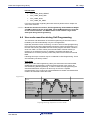
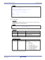
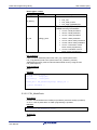
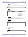
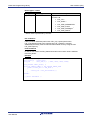
Device Reprogramming is disabled if FLMD0 Pin is low. By using a port pin or an
external logic FLMD0 must be set to “1” to allow Self-Programming. Additionally
reprogramming can be enabled by a register if supported by the device. Please
refer to the device user manual for further details.
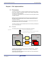
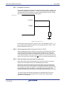
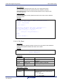
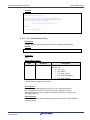
Figure 4-2
Port-Pin
FLMD0
R
Vss
FLMD0 sample circuit
In the sample circuit, the port pin is input on reset. Thus FLMD0 is held to VSS on
reset. During Self-Programming the port is set to output and to the value “1”. By
that the FLMD0 pin is set to VDD.
4.2.2
Normal operation (Error Correction Circuit – ECC)
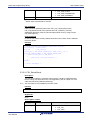
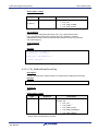
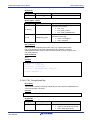
RC03F based Flash devices contain Error Correction Circuits (ECC) to provide
correct Flash data. During Flash write operations, beside the user data, also
redundant ECC data is written into additional Flash cells in order to be able to
correct detected Flash errors during Flash read. ECC is an on-line method. That
means from user point of view ECC has no impact on the data read performance.
4.2.3
Safe reprogramming using Self-Programming
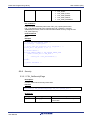
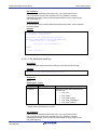
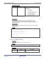
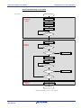
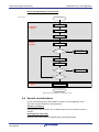
When talking about safe Self-Programming, that naming needs to be exactly
defined, as several different ways of understanding are possible.
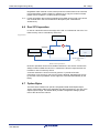
Basic idea of safe Self-Programming is that if anything during reprogramming
process goes wrong, it must be possible to keep basic application functionality
alive. Usually it is solved by separation of the application into the application that
is updated and therefore temporarily not valid during reprogramming, and a
specific bootloader that must always be executable again after power up or reset.
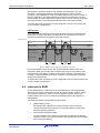
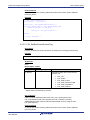
Two major options with different advantages and disadvantages have to be
considered. Depending on the application and bootloader the appropriate
solution has to be selected:
R01US0046ED Rev. 1.01
User Manual
19