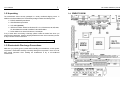
1
I
User’s Manual
ENDAT-3205M/S
User’s Manual
Rev. 2C
II
The ENDAT-3205M/S System Board
Copyright Notice
The content of this manual has been checked for accuracy. The manufacturer
assumes no responsibility for any inaccuracies that may be contained in this
manual. The manufacturer reserves the right to make improvements or
modification to this document and/or the product at any time without prior
notice. No part of this document may be reproduced, transmitted, photocopied or
translated into any language, in any form or by any means, electronic, mechanical,
magnetic, optical or chemical, without the prior written permission of the
manufacturer.
VIA is registered trademark of VIA Technology Incorporation
VT82C686B may only be used to identify products of VIA Technology
Realtek is registered trademark of Realtek Technologies Inc.
Multiscan is a trademark of Sony Corp of America
IBM, EGA, VGA, PC/XT, PC/AT, OS/2 and PS/2 are registered trademarks of
International Business Machines Corporation
Intel is a registered trademark of Intel Corporation
Plug and Play is registered trademarks of Intel Corporation
Microsoft, Windows and MS-DOS are trademarks of Microsoft Corporation
AMI is a trademark of American Megatrends Inc.
PCI is a registered trademark of PCI Special Interest Group
Other product names mentioned herein are used for identification purpose only and
may be trademarks and/or registered trademarks of their respective companies.
Installation Notice
For 3205M PCB ver. 1D or later
3205S PCB ver: 1B or later
11/02/2005
The manufacturer recommends using a grounded plug to ensure proper
motherboard operation. Care should be used in proper conjunction with a
grounded power receptacle to avoid possible electrical shock. All integrated circuits
on this motherboard are sensitive to static electricity. To avoid damaging
components from electrostatic discharge, please do not remove the board from the
anti-static packing before discharging any static electricity to your body, by wearing
a wrist-grounding strap. The manufacturer is not responsible for any damage to the
motherboard due to improper operation.
III
User’s Manual
IV
Specification:
This manual covers three different layout models, and the respective board layouts
are shown in chapter 1-4 and 1-5. Please refer to the following description to make
sure which model on hand before using.
Model
Form Factor
CPU
Supporting
LAN Adapter
IDE Connector
FDD Connector
AC97’ Audio
ENDAT-3205M
ENDAT-3205S
Mini-ITX 170 mm x 170 mm (6.69”x6.69”)
Embedded VIA Low Power
Consumption C3 series (FAN
required) / Eden Series (FAN-less)
Socket370 Intel Tualatin/
Pentium3/Celeron/VIA C3
Realtek 8139D or Intel 82551QM
10/100 Based LAN
Realtek 8139D only for both of LAN
chip, LAN2 is optional
2 x 40pin IDE connectors support
UDMA 33/66/100, 1 x 44pin
connector support Slim type HDD
(share to IDE1)
1 x FDD connector
2 x 40pin IDE connectors support
UDMA 33/66/100, 1x CF socket by
optional
N/A
Phone Jack + Pin Header
Phone Jack + Pin Header
Wafer only
Wafer only
Cash Drawer
System Chipset
DIMM Socket
VGA Adapter
VIA ProSavage4 AGP4x 2D/3D Graphic Controller w/ SMA 8/16/32MB
Display ratio
4:3 and 16:9
LCD
Supporting
8, 16, 24bit CSTN/ DSTN LCD panel with TTL interface
9, 12, 18, 24, 36 TFT LCD Panel with TTL interface
18, 24, 36bit LVDS interface (24bit LVDS is optional)
I/O Port
Digital IO
WDT
RS-422/485
4 x COMs w/+5V, +12V selector /1 x Parallel port
VIA VT8606 + VIA VT82C686B
One DIMM Socket supports 512MB
6 bit Digital Input (optional)/ 2 bit Output
1 to 255 seconds S/W programmable by optional feature
Optional via COM2
Expansion Slot
1x120Pin PCI connector + Intel Embedded ATX edge connector for three
PCI slot expansion via riser card
USB Port
Power Supply
4 x USB1.1 onboard
ATX power support
The ENDAT-3205M/S System Board
TABLE OF CONTENTS
CHAPTER 1. INTRODUCTION ....................................................... 1
1-1.
1-2.
1-3.
1-4.
1-5.
FEATURES .............................................................................................. 3
UNPACKING ............................................................................................ 5
ELECTROSTATIC DISCHARGE PRECAUTIONS ................................... 5
MOTHERBOARD LAYOUT (ENDAT-3205M)........................................... 6
MOTHERBOARD LAYOUT (ENDAT-3205S) .......................................... 7
CHAPTER 2. SETTING UP THE MOTHERBOARD ....................... 8
2-1. JUMPERS AND CONNECTORS (ENDAT-3205M)................................... 8
2-2. JUMPERS AND CONNECTORS (ENDAT-3205S) ................................. 15
2-3. INSTALLING MEMORY.......................................................................... 22
2-4. SHARED VGA MEMORY ....................................................................... 22
2-5. INSTALLING RISER CARD.................................................................... 22
2-6. ASSIGNING IRQs FOR EXPANSION CARDS ....................................... 22
2-7. WATCH DOG TIMER………………………………………………………….24
2-8 DIGITAL I/O AND CASH DRAWER…………………………………………..25
CHAPTER 3. AWARD BIOS SETUP............................................. 28
3-1. STANDARD COMS FEATURES............................................................. 28
3-2. ADVANCED BIOS FEATURES............................................................... 29
3-3. ADVANCED CHIPSET FEATURES ........................................................ 31
3-4. INTEGRATED PERIPHERALS............................................................... 34
3-5. POWER MANAGEMENT SETUP........................................................... 36
3-6. PnP/PCI CONFIGURATIONS................................................................. 39
3-7. PC HEALTH STATUS ............................................................................. 40
User’s Manual
V
CHPATER 4. VGA, LCD, FEATURE.............................................. 41
4-1. AGP-BUS VGA FEATURE...................................................................... 41
4-2. LCD FLAT PANEL FEATURE ................................................................. 42
4-3. PCI BUS AUDIO ADAPTER FEATURES................................................ 43
4-4. DRIVER UTILITY INSTALLATION GUIDE ............................................. 44
CHPATER 5. LAN ADAPTER ........................................................ 46
5-1. FEATURES ............................................................................................ 46
5-2. UTP CABLE/RJ-45 JACK DEFINITION .................................................. 47
5-3. CONNECTING 100BASE-TX FAST ETHERNET NETWORK ................ 48
5-4. CONNECTING 10BASE-T ETHERNET NETWORK .............................. 48
5-5. 10MBASE/ 100MBASE INSTALLATION NOTICE .................................. 48
5-6. REMOTE BOOT ROM FUNCTION ........................................................ 49
5-7. LED INDICATORS.................................................................................. 49
5-8. THE SETUP PROGRAM ....................................................................... 50
APPENDIX A: FLASH MEMORY UTILITY.................................... 52
APPENDIX B: CONNECTOR PIN ASSIGNMENT ........................ 53
APPENDIX C: LIMITED WARRANTY ........................................... 65
User’s Manual
1
Chapter 1. Introduction
In order to cope with the challenges of the system heating issues and demand of much more
diminutive embedded system in diverse application, ENDAT-3205M system board provides
the ultimate solution by integrating with VIA’s technology low power consumption VIA C3
series (FAN required) CPUs and VIA Eden (FAN-less) series CPUs. ENDAT-3205M not only
provide the ideal solution for Hi-End POS system, but also can be adapted in various
applications such as kiosks, networking systems, controlling terminals and other embedded
systems.
To provide higher performance solution, The ENDAT-3205S system board provides
the ultimate design support the INTEL Tualatin / PIII / Celeron CPUs.
ENDAT-3205M is highly integrated industrial grade system board to support
133/100/66 MHz CPU FSB (“Front Side Bus”) frequency and based on 64-bit to
support VIA C3 / Eden series embedded processors.
ENDAT-3205M / ENDAT-3205S are designed with VT8606 “Twister-T” North
Bridge and the VT82c686B Super South Bridge. Support One DIMM Socket of
DRAM up to 512MBbyte of system memory with 256Mbit DRAM technology. The
DRAM controller supports standard PC133 and PC100 Synchronous DRAM
(SDRAM). The DRAM bank can be composed of an arbitrary mixture of 1M / 2M /
4M / 8M / 16M / 32MxN DRAMs. The DRAM controller can run at either the host
CPU FSB at 133/100 MHz.
ENDAT-3205M/S are integrate S3 Graphics’ 128-bit ProSavage4 graphics
accelerator which support mainstream graphics perform with leading-edge 2D, 3D
and DVD video acceleration. Based on its integrated AGP 4X solution, and support
the Microsoft DirectX Texture Compression (DXTC) to deliver unprecedented 3D
performance and image quality. With utilizes a single cycle architecture that
provides high performance along with superior image quality. Several new features
to enhance 3D architecture, including single-pass multi-texturing, anisotropy
filtering, and an 8-bit stencil buffer to enable stunning image quality without losing
on performance.
ENDAT-3205M/S strongly supports a wide variety of DSTN or TFT panels through a
36-bit TTL/CMOS interface from 4:3 and 16:9 mode displays. Which include VGA,
SVGA, XGA, and SXGA+ TFT color panels with 9-bit, 12-bit, 18-bit (both 1
2
The ENDAT-3205M/S System Board
pixel/clock and 2 pixels/clock), and 24-bit TTL/CMOS interfaces. Its enhanced STN
hardware with 256 gray scale support and advanced frame rate control can provide
up to 16.7 million colors. In addition, the integrated 2-channel LVDS interface can
support 18-bit (36-bit) color panels. All resolutions are supported up to SXGA+
(1400x1050).
ENDAT-3205M/S provides standard PCI slot with Intel embedded ATX defined can
support more than 2 PCI expansions via the edge connector along with the
standard onboard PCI slot. This board is not only fully compatible with industry
standards, but also thousand of software application; such as WIN 95, 98, WIN ME,
WIN XP, WIN NT 3.x / 4.x, WIN 2000, WIN CE (.NET), Linux, UNIX, Novell…etc.
The control logic provides high-speed performance for the most advance multi-user,
multitasking application. Tomorrow’s PC technology is here today.
The ideal solution of ENDAT-3205M/ ENDAT-3205S
- POS system
- KIOSK
- Interactive system
- Airport Terminal Controller
- Industrial controller
- Digital entertainment
- Embedded system equipment
User’s Manual
3
4
The ENDAT-3205M/S System Board
Ordering information:
1-1. Features
Basic Feature:
z
z
z
z
z
z
z
z
z
z
z
z
ENDAT-3205M: supports VIA EBGA type of C3 / Eden series
processors with 133/100/66 MHz Front Side Bus (FSB)
ENDAT-3205S: supports Socket370 Intel Tualatin / Pentium III /
Celeron / FCPGA / FCPGA2 series processors with 133/100/66 MHz
Front Side Bus (FSB)
DRAM interface runs synchronous (133/133 or 100/100) mode.
Supports standard PC133 and PC100 SDRAM up to 512MB
Full internal AGP 4x performance with 8/16/32 MB frame buffer
share with system memory
Integrated ProSavage4 2D/3D/Video Accelerator, with next
generation, 128-bit 2D graphics engine resolutions up to 1920x1440
Direct Flat panel interface support 36-bit DSTN/TFT flat panel
interface support 4:3 and 16:9 display, with 256 gray shade support
up to SXGA+(1920x1400x16)
Integrated 2-channel 110 MHz LVDS interface
Simultaneous display of CRT with LCD Panel
6 bit digital input / 2 bit output
Built-in Cash drawer controller.
AC97’ Audio support with 1.5W amplifier built-in
Full Software Support
z Drivers for major operating systems and APIs: Windows 9x / ME,
Windows NT 4.0, Windows 2000, Windows XP, Direct3D,
DirectDraw and DirectShow, OpenGL ICD for Windows 9x, NT, and
2000, and DXVA for Windows 2000 and Windows XP
ENDAT-3205M
1. ENDAT-3205M-1R-10: Supports 1 Realtek LAN, C3 1GHz, LVDS
18 and 36 bits
2.
ENDAT-3205M-1RL-10: Supports 1 Realtek LAN, C3 1GHz, and
LVDS 24 bits
3.
ENDAT-3205M-1R-E8: Supports 1 Realtek LAN, Eden ESP8000,
LVDS 18 and 36 bits
4.
ENDAT-3205M-1RL-E8: Supports 1 Realtek LAN, Eden ESP8000,
and LVDS 24 bits
ENDAT-3205S
1. ENDAT-3205S-1R: Support 1 Realtek LAN, LVDS 18 and 36 bits
2. ENDAT-3205S-1RL: Support 1 Realtek LAN and LVDS 24 bits
3. ENDAT-3205S-2R: Support 2 Realtek LAN, LVDS 18 and 36 bits
4. ENDAT-3205S-2RL: Support 2 Realtek LAN and LVDS 24 bits
Note:
1.
The standard version of ENDAT-3205M is embedded with VIA C3 1 GHz and
one Realtek LAN chip. Other option will be provided upon request.
2.
All VIA C3 series and Socket 370 type CPUs are Heat sink and FAN required.
User’s Manual
5
1-2. Unpacking
The motherboard comes securely packaged in a sturdy cardboard shipping carton. In
addition to the User's Manual, the motherboard package includes the following items:
•
•
•
•
ENDAT-3205M/S System Board
HDD/FDD/Serial port Cables
LCD cable (Optional)
IDE Driver includes: Drivers for Windows NT 3.x/4.x, Windows 95, 98, ME, 2000,
XP, Novell Netware and AMI / AWARD FLASH ROM utilities.
• Driver utilities for on-board VGA drivers, LAN adapter
If any of these items are missing or damage, please contact the dealer from whom you
purchase the motherboard. Save the shipping material and carton in the event that you want
to ship or store the board in the future.
Note: Leave the motherboard in its original package until you are ready to install it!
1-3. Electrostatic Discharge Precautions
Make sure you properly ground yourself before handling the motherboard, or other system
components. Electrostatic discharge can easily damage the components. Note: You must
take special precaution when handling the motherboard in dry or air-conditioned
environments.
6
1-4. ENDAT-3205M
The ENDAT-3205M/S System Board
User’s Manual
1-5. ENDAT-3205S
7
8
The ENDAT-3205M/S System Board
Chapter 2. Setting up the Motherboard
2-1. Jumpers and Connectors (ENDAT-3205M)
Jumpers/Connectors Overview:
Function
Jumpers/Connectors
Cooling Fan Connector
JFAN1, JFAN2
LAN Adapter Disable/Enable
JP1
COM Ports Power Selector (COM1, 2, 3, 4) JP5, JP10
RS232/RS422/RS485 Selector (COM2)
JP8, JP9
LCD: TFT LCD Panel Connector
LCD_C1, LCD_C2
LVDS LCD Output Port
LVDS1
24 bit LVDS trigger edge
JP3: Pin 1, 3, 5
LVDS backlight power/control
CN3
TFT LCD Voltage Selector
JP2, JP3: Pin 2, 4, 6
LCD clock timing adjustment
JP4
Internal VGA port
CN5
COM4 Box header
CN7
MIC IN, LINE IN, CD IN
CN10, CN11, CN12
Speaker out / internal speaker out
CN9, CN13
Digital I/O header
JP7
Cash drawer connector
CN4
Clear CMOS
JBAT1
Factory default
SW1, JP6: Pin 9~11
PS/2 Mouse/KB Pin Header
CN1, JKBMS2
OEM MS/KB Header
JKBM2
IR
CN8
USB Port (0-3)
JRJ1A, JUSB1
LAN port
JRJ1B
FDD Connector
FDD1
IDE 1, IDE2
IDE1, IDE2
Slim IDE
IDEB1
9
User’s Manual
Function
Header for Case Panel
IDE LED
External Speaker
Buzzer On/Off
Hardware Reset Switch
Power Good Select: External PG
Internal PG
ATX Power Supply On/Off Switch
Power LED
Jumpers/Connectors
JP6
JP6: Pin 1 (–), Pin 2 (+)
JP6: Pin 3, Pin 6
JP6: Pin 4, Pin 5
JP6: Pin 7, Pin 8
JP6: Pin 9-10
JP6: Pin 10-11
JP6: Pin 12, Pin 13
JP6: Pin 14 (–), Pin 15 (+)
Please double-check the insertion and orientation of the LCD cable before applying power.
Improper installation will result in permanent damage LCD panel.
Part 1: Onboard Jumpers
JP1: On-board LAN Disable/Enable (2.0mm)
Enable *
Close Pin 1-2
Disable
Close Pin 2-3
JBAT1: CMOS Data Clear (2.0mm)
Pin 1-2 Close for clear CMOS, the default setting is OPEN.
JP8, JP9: RS232 / 422 / 485 Selector for COM2 (2.0mm)
TYPE
JP8 (3x4/2mm)
JP9 (2x7/2mm)
RS-232 *
1-2, 4-5, 7-8, 10-11
1-2
RS-422/485 (2 wire) 2-3, 5-6, 8-9, 11-12
5-6, 9-11, 10-12
RS-422/485 (4 wire) 2-3, 5-6, 8-9, 11-12
3-4, 7-8
* Make sure the port mode has been set up correctly before installing any peripherals.
JP5 (COM1, 2) / JP10 (COM3, 4) Voltage Selector (2.0mm)
Voltage COM1 (JP5) COM2 (JP5) COM3 (JP10) COM4 (JP10)
1-2
7-8
1-2
7-8
+12V(DC)
3-4
9-10
3-4
9-10
R.I. *
5-6
11-12
5-6
11-12
+5V(DC)
10
The ENDAT-3205M/S System Board
JP6: Case Panel Connection (2.54mm)
Pin No.
Description
HDD_LED (1:LED–, 2:LED+)
1-2
PC speaker
3-6
Onboard Buzzer
4-5 *
Hardware RESET
7-8
9-10: External PG, 10-11: Internal PG
9-10-11
Power On/Off
12-13
Power LED (14:LED-, 15:LED+)
14-15
JP3 (Pin 2, 4, 6), JP2: Voltage Selector for LCD panel
LCD power
JP2 (2.54mm)
JP3 (2.0mm)
VDDLCD is 5V
Open
Close 2-4
VDDLCD is 3.3V *
Open
Close 4-6
VDDLCD is 12V
Close
Pin 2, 4, 6 must Open
Caution: Improper setting will damage LCD panel.
JP3 (Pin 1, 3, 5): 24 bit on-board LVDS trigger edge selector (2.0mm)
Pin No.
Function
Rising edge
1,3 *
Falling edge
3,5
JP4: LCD Panel clock timing adjustment (2.0mm).
Pin No.
Function
1,2 *
No delay
3,4
Delay 5n Sec
5,6
Delay 10n Sec
7,8
Delay 15n Sec
9,10
Delay 20n Sec
11,12
Delay 25n Sec
11
User’s Manual
Part 2: Onboard connectors
JFAN1, JFAN2: CPU / 2nd Cooling Fan Connector
Pin No.
Function
Sensor Pin.
1
+12V
2
GND
3
Box Header Type Connector for COM port (RS-232)
Pin No.
Function
Pin No.
Function
DCD
DSR
1
6
RXD
RTS
2
7
TXD
CTS
3
8
DTR
RI
4
9
GND
N.C
5
10
D-SUB Type Connector for COM2 port (RS-422Æ 4 Wire)
Pin No.
1
2
3
4
5
Function
–TXD
+RXD
+TXD
NA
NA
Pin No.
6
7
8
9
Function
NA
NA
NA
–RXD
D-SUB Type Connector for COM2 port (RS-485Æ 2 Wire)
Pin No.
1
2
3
4
5
Function
Data –
NA
Data +
NA
NA
Pin No.
6
7
8
9
J1: IR Connector (2.54mm)
VCC
Pin 1
Pin 4
N.C
Pin 2
Pin 5
IRRX
Pin 3
Function
NA
NA
NA
NA
GND
IRTX
12
The ENDAT-3205M/S System Board
CN7: PS/2 Keyboard / Mouse Pin Header Connector (2.54mm)
Pin No.
Signal (KB)
Pin No.
Signal (MS)
1
KB Data
2
MS Data
3
KEY
4
KEY
5
GND
6
GND
7
+5V(DC)
8
+5V(DC)
9
KB_CLK
10
MS_CLK
JKBMS2: Pin Header for external device (2.0mm)
Pin No.
Signal (KB)
Pin No.
Signal (MS)
KB Data Out
MS Data Out
1
2
KB Data In
MS Data In
3
4
KB CK Out
MS Data Out
5
6
KB CK In
MS CK In
7
8
KEY
KEY
9
10
+5V(DC)
+5V(DC)
11
12
GND
GND
13
14
Default setting is: 1-3, 5-7, 2-4 and 6-8 close.
JUSB1: USB port 2, 3 (2.54mm)
Pin No.
Function
Pin No.
USB2_VCC
1
2
USBD2–
3
4
USBD2+
5
6
USB_GND2
7
8
USB_GND2
9
10
Function
USB3_VCC
USBD3–
USBD3+
USB_GND3
USB_GND3
CN12: CD IN (2.54mm)
Pin No.
Function
LEFT
1
GND
3
Pin No.
2
4
Function
GND
RIGHT
CN11: LINE IN (2.54mm)
Pin No.
Function
RIGHT
1
GND
3
Pin No.
2
4
Function
GND
LEFT
13
User’s Manual
CN10: Microphone IN (2.54mm)
Pin No.
Function
Pin No.
1
MIC POWER
2
3
GND
4
Function
GND
MIC IN
CN13: Internal speaker out (2.54mm)
Pin No.
Function
Pin No.
RIGHT
1
2
GND
3
4
Function
GND
LEFT
JP7: Digital I/O connector (2.54mm)
Pin No.
Function
Pin No.
OUT0
1
2
OUT1
3
4
INPUT4
5
6
INPUT5
7
8
+12V
9
10
KEY
11
12
GND
13
14
Function
INPUT0
INPUT1
INPUT2
INPUT3
+12V
+5V
GND
14
The ENDAT-3205M/S System Board
CN5: Internal VGA Connector (2.54mm)
CN4: Cash drawer connector (JST connector)
Pin No.
Function
DRAWER1
1
SENSOR
2
+12V
3
DRAWER2
4
GND
5
CN3: LCD - LVDS backlight power and ON/OFF control (JST connector)
Pin No.
Function
VBL (+12V)
1
VBL (+12V)
2
ON (+5V)/OFF (GND)
3
GND
4
GND
5
Pin No.
1
2
3
4
5
6
7
8
Description
RED
GREEN
BLUE
N.C
GND
GND
GND
GND
Pin No.
9
10
11
12
13
14
15
Description
N.C / +5V
GND
N.C
DDC DAT
H-Sync
V-Sync
DDC CLK
Note: Please refer to the appendix B for data mapping of LCD connector
User’s Manual
2-2. Jumpers and Connectors (ENDAT-3205S)
Jumpers/Connectors Overview:
Function
Jumpers/Connectors
Cooling Fan Connector
JFAN1, JFAN2
LAN Adapter Disable/Enable
JP12
COM Ports Power Selector (COM1, 2, 3, 4) JP4, JP10
RS232/RS422/RS485 Selector (COM2)
JP5, JP9
LCD: TFT LCD Panel Connector
LCD_C1, LCD_C2
LVDS LCD Output Port
LVDS1
24 bit LVDS trigger edge
JP1: Pin 1, 3, 5
LVDS backlight power/control
CN1
TFT LCD Voltage Selector
JP1: Pin 2,4, 6, JP2
LCD clock timing adjustment
JP3
Internal VGA port
CN4
COM4 Box header
CN7
MIC IN, LINE IN, CD IN
CN11, CN10, CN9
Speaker out / internal speaker out
CN8, CN14
nd
2 LAN header
CN12
Digital I/O header
JP7
Cash drawer connector
CN5
Clear CMOS
JBAT1
Factory default
JP6, JP8
PS/2 Mouse/ KB Pin Header
CN2, JKBMS1
IR
CN13
USB Port (0-3)
JRJ1A, JUSB1
LAN port
JRJ1B
IDE 1, IDE2
IDE1, IDE2
CF Master/Slave select
JP11
JP13
Header for Case Panel
JP13: Pin 1 (–), Pin 2 (+)
IDE LED
External Speaker
JP13: Pin 3, Pin 6
Buzzer On/Off
JP13: Pin 4, Pin 5
15
16
The ENDAT-3205M/S System Board
Function
Hardware Reset Switch
Power Good Select: External PG
Internal PG
ATX Power Supply On/Off Switch
Power LED
Watch Dog Timer enable Switch
Jumpers/Connectors
JP13: Pin 7, Pin 8
JP13: Pin 9-10
JP13: Pin 10-11
JP13: Pin 12, Pin 13
JP13: Pin 14 (–), Pin 15 (+)
JP13: Pin 16, Pin 17
Please double-check the insertion and orientation of the LCD cable before applying power.
Improper installation will result in permanent damage LCD panel.
Part 1: Onboard Jumpers
JP12: LAN Enable / Disable:
Pin No.
Function
1-2 *
LAN1 Enable
2-3
LAN1 Disable
4-5 *
LAN2 Enable
5-6
LAN2 Disable
JBAT1: CMOS Data Clear:
Pin 1-2 Close for clear CMOS, the default setting is OPEN.
JP5, JP9: RS232 / 422 / 485 Selector for COM2:
TYPE
JP9 (3x4/2mm)
JP5 (2x7/2mm)
1-2, 4-5, 7-8, 10-11
1-2
RS-232 *
5-6, 9-11, 10-12
RS-422/485 (2 wire) 2-3, 5-6, 8-9, 11-12
3-4, 7-8
RS-422/485 (4 wire) 2-3, 5-6, 8-9, 11-12
* Make sure the port mode has been set up correctly before installing any peripherals.
JP4 (COM1, 2) / JP10 (COM3, 4) Voltage Selector:
Voltage COM1 (JP4) COM2 (JP4) COM3 (JP10) COM4 (JP10)
1-2
7-8
1-2
7-8
+12V(DC)
3-4
9-10
3-4
9-10
R.I. *
5-6
11-12
5-6
11-12
+5V(DC)
User’s Manual
JP13: Case Panel Connection:
Pin No.
Description
HDD_LED (1:LED–, 2:LED+)
1-2
3-6
PC speaker
4-5 *
Onboard Buzzer
7-8
Hardware RESET
9-10-11
9-10: External PG, 10-11: Internal PG
Power On/Off
12-13
Power LED (14:LED-, 15:LED+)
14-15
Watch Dog Timer Enable
16-17
JP1: LCD power selector / Onboard 24bit LVDS trigger edge:
LCD Power (+Volts) JP1
JP2
Pin No (JP2)
Function
Rising edge
3.3 *
4-6
Open
1-3 *
Falling edge
5
1-3
Open
3-5
12
Open Close
Caution: Improper setting will damage LCD panel.
17
18
The ENDAT-3205M/S System Board
Part 2: Onboard connectors
JFAN1, JFAN2: CPU / 2nd Cooling Fan Connector:
Pin No.
Function
Sensor Pin.
1
+12V
2
GND
3
Box Header Type Connector for COM port (RS-232)
Pin No.
Function
Pin No.
Function
DCD
DSR
1
6
RXD
RTS
2
7
TXD
CTS
3
8
DTR
RI
4
9
GND
N.C
5
10
D-SUB Type Connector for COM2 port (RS-422Æ 4 Wire)
JP3: LCD Panel clock timing adjustment (2.0mm):
Pin No.
Function
1-2 *
No delay
3-4
Delay 5n Sec
5-6
Delay 10n Sec
7-8
Delay 15n Sec
9-10
Delay 20n Sec
11-12
Delay 25n Sec
JP11: CF Master/Slave select:
Pin No
Function
Slave
1-2 *
Master
2-3
Pin No.
1
2
3
4
5
Function
–TXD
+RXD
+TXD
NA
NA
Pin No.
6
7
8
9
Function
NA
NA
NA
–RXD
D-SUB Type Connector for COM2 port (RS-485Æ 2 Wire)
Pin No.
1
2
3
4
5
Function
Data –
NA
Data +
NA
NA
Pin No.
6
7
8
9
CN13: IR Connector (2.54mm)
VCC
Pin 1
Pin 4
N.C
Pin 2
Pin 5
IRRX
Pin 3
Function
NA
NA
NA
NA
GND
IRTX
19
User’s Manual
CN2: PS/2 Keyboard / Mouse Pin Header Connector (2.54mm)
Pin No.
Signal (KB)
Pin No.
Signal (MS)
1
KB Data
2
MS Data
3
KEY
4
KEY
5
GND
6
GND
7
+5V(DC)
8
+5V(DC)
9
KB_CLK
10
MS_CLK
JKBMS2: Pin Header for external device (2.0mm)
Pin No.
Signal (KB)
Pin No.
Signal (MS)
KB Data Out
MS Data Out
1
2
KB Data In
MS Data In
3
4
KB CK Out
MS Data Out
5
6
KB CK In
MS CK In
7
8
KEY
KEY
9
10
+5V(DC)
+5V(DC)
11
12
GND
GND
13
14
Default setting is: 1-3, 5-7, 2-4 and 6-8 close.
JUSB1: USB port 2, 3 (2.54mm)
Pin No.
Function
Pin No.
USB2_VCC
1
2
USBD2–
3
4
USBD2+
5
6
USB_GND2
7
8
USB_GND2
9
10
Function
USB3_VCC
USBD3–
USBD3+
USB_GND3
USB_GND3
CN9: CD IN (2.54mm)
Pin No.
Function
LEFT
1
GND
3
Pin No.
2
4
Function
GND
RIGHT
CN10: LINE IN (2.54mm)
Pin No.
Function
RIGHT
1
GND
3
Pin No.
2
4
Function
GND
LEFT
20
The ENDAT-3205M/S System Board
CN11: Microphone IN (2.54mm)
Pin No.
Function
Pin No.
1
MIC POWER
2
3
GND
4
Function
GND
MIC IN
CN14: Internal speaker out (2.54mm)
Pin No.
Function
Pin No.
RIGHT
1
2
GND
3
4
Function
GND
LEFT
JP7: Digital I/O connector (2.0mm)
Pin No.
Function
Pin No.
OUT0
1
2
OUT1
3
4
INPUT4
5
6
INPUT5
7
8
+12V
9
10
KEY
11
12
GND
13
14
Function
INPUT0
INPUT1
INPUT2
INPUT3
+12V
+5V
GND
CN5: Cash drawer connector (2.54mm)
Pin No.
Function
DRAWER1
1
SENSOR
2
+12V
3
DRAWER2
4
GND
5
CN1: LCD - LVDS backlight power and ON/OFF control (JST connector)
Pin No.
Function
VBL (+12V)
1
VBL (+12V)
2
ON (+5V)/OFF (GND)
3
GND
4
GND
5
21
User’s Manual
CN4: Internal VGA Connector (2.0mm)
Pin No.
1
2
3
4
5
6
7
8
Description
RED
GREEN
BLUE
N.C
GND
GND
GND
GND
Pin No.
9
10
11
12
13
14
15
Description
N.C / +5V
GND
N.C
DDC DAT
H-Sync
V-Sync
DDC CLK
Note: Please refer to the appendix B for data mapping of LCD connector
22
The ENDAT-3205M/S System Board
2-3. Installing Memory
The ENDAT-3205M/S CPU board offers one 168pin DIMM socket supporting up to 512MB of
memory. The DIMM memory can be 100MHz (PC-100) or 133 MHz (PC-133).
2-4. Shared VGA Memory
The ENDAT-3205M/S is using built-in AGP VGA controller with Share Memory Architecture
(SMA) - AGP mode with up to 32MB of system memory. The amount of video memory on
motherboard determines the number of colors and the video graphic resolution.
2-5. Installing Riser Card
Installing Riser Card (Max. 2 PCI Slots on Riser Card)
PCI Slot
INT
ADSEL
PCI 1 A,B,C,D
AD24
PCI 2 B,C,D,A
AD23
PCI 3 C,D,A,B
AD22
PCI 4 D,A,B,C
AD21 (On Board LAN)
The default INT/AD-select for ENDAT-3205M/S All-In-One motherboard is listed in the above
table.
2-6. Assigning IRQs for Expansion Cards
The IRQ number is automatically assigned to PCI expansion cards after those used by
onboard device. To install a PCI riser card, you need to set the correct "ADSEL" and "INT"
(interrupt) assignment. Please refer to "Chapter 2-5" Installing Riser Card for detail
assignments.
23
User’s Manual
IRQ
0
1
2
3
4
5
6
7
8
9
10
11
12
13
14
15
Status
Used
Used
Used
Used
Used
Used
Used
Used
Used
Used
Used
Used
Used
Used
Used
Used
Assignment
Timer
Keyboard
Second 8259
COM2
COM1
COM3
Floppy Disk
LPT1
RTC
LPT2 or Audio
COM4
LAN Adapter (on board)
PS/2 Mouse
Coprocessor
Hard Disk (IDE 1)
Reserved (IDE 2)
24
The ENDAT-3205M/S System Board
2-7. Watch Dog Timer (optional function)
Watch Dog Timer (WDT) is a special design for system to monitor and secure that
system can work normally. WDT is used an independent ISA device for support this
function. When time is up, WDT would send hardware RESET signal to reset
system.
Operators need to write a value into WDT port. The detailed operate instruction is
shown below:
WDT port address
305h (1 byte data)
306h (address trigger)
307h (address trigger)
308h (address trigger)
FUNCTION DESCRIPTION
Set the time up value (1-255), unit: SEC
Enable WDT
Disable WDT
Refresh/ clear WDT counter
WDT Setup Procedure:
1) Disable WDT:
Please make sure WDT is not working before process. Send one byte (any
value) into system address (307H) to disable WDT working status.
The sample code is shown below (using TurboC/C++ 3.0):
#define WDT_DISABLE 0x307
outportb(WDT_DISABLE,0x0);
2) Set a time-up value by 305H:
Set the time-up value to WDT. The unit is second and range from 1 to 255 seconds.
The sample code is shown below (using TurboC/C++ 3.0):
#define WDT_TIME_VALUE 0x307
#define WDT_TIME_UP_VALUE 10
outportb(WDT_TIME,WDT_TIME_UP_VALUE);
3) Enable WDT:
Enable WDT counter “on” and start increasing counter. Send one byte (any
value) into system address (306H) to enable WDT.
The sample code is show below (using TurboC/C++ 3.0):
#define WDT_ENABLE 0x306
outportb(WDT_ENABLE,0x0);
25
User’s Manual
4) REFRESH/CLEAR WDT:
The ENDAT-3205M/S System Board
3) Digital output control port:
Repeatedly write WDT REFRESH port (308H) with any data and the interval
cannot be longer than the preset time. Otherwise, WDT will send hardware
RESET signal to reset system.
The sample code is shown below (using TurboC/C++ 3.0):
#define WDT_REFRESH 0x308
outportb(WDT_REFRESH,0x0);
2-8. Digital I/O & Cash Drawer control (Optional feature for
input, function combined with WDT H/W)
1) Pin out of digital I/O header (JP7):
Pin No.
Function
OUT0
1
OUT1
3
INPUT4
5
INPUT5
7
+12V
9
KEY
11
GND
13
26
This function is built in the system South-Bridge. ENDAT-3205x can offer 2
different logic level (3.3V and 12V) outputs at the same time.
The digital output port can be written directly by porting address “404Eh” and
the default value is “00h (data mapping to bit6 for OUT1 and bit7 for OUT0)”.
The JP7 only provides 0V/3.3V and CN4 only provides 0V/12V output.
The sample code is shown below (using TurboC/C++ 3.0):
#define OUT_PORT 0x404e
outportb(OUT_PORT,0x80); //Set OUT0 as logic “1” and OUT1 as “0”
outportb(OUT_PORT,0x40); //Set OUT1 as logic “1” and OUT0 as “0”
outportb(OUT_PORT,0xc0); //Set OUT0 and OUT1 as logic “1”
4) Cash drawer port:
Pin No.
2
4
6
8
10
12
14
Function
INPUT0
INPUT1
INPUT2
INPUT3
+12V
+5V
GND
2) Digital input control port:
The digital input function and WDT function are both supported by H/W WDT
chip. Either one cannot work without H/W WDT chip!
The digital input port can be read directly from port address “30Ah” and the
default value is “FFh (data mapping to bit0 to bit5)”. ENDAT-3205x is with
onboard pull-up resistors (4.7K ohm to +5V) and decoupling capacitor (180pF
to system GROUND) for each input pin to prevent any unexpected noise. The
input level is 2.5V, 3.3V and 5V (+/-5% range).
The sample code is shown below (using TurboC/C++ 3.0):
#define INPUT_PORT 0x30a
unsigned char read_data;
read_data=inportb(INPUT_PORT); //Read status from INPUT port
Attention: The WDT chip might be damaged by over specifying voltage.
a). Pin out of cash drawer connector (internal JST connector):
Pin No.
Function
1
DRAWER1
2
SENSOR
3
+12V
4
DRAWER2
5
GND
b). Digital output control port:
This function offers 2 controls (0V/+12V) to open the cash drawer. It can be
used for DIGITAL I/O control with 0V/+12V level also. The input level of
SENSOR pin (pin2) must be 12V, and the SENSOR pin can be read from
bit0 of DIGITAL INPUT port.
The sample code is shown below (using TurboC/C++ 3.0):
#define OUT_PORT 0x404e
#define INPUT_PORT 0x30a
unsigned char read_data;
outportb(OUT_PORT,0xc0); //Set all cash drawer not open (+12V)
outportb(OUT_PORT,0x40); //Set DRAWER1 open (0V)
outportb(OUT_PORT,0x80); //Set DRAWER2 open (0V)
outportb(OUT_PORT,0x00); //Set all cash drawer open (0V)
read_data=inportb(INPUT_PORT); //Read status from INPUT port
read_data=read_data&0x01; //Get the status of sensor
27
User’s Manual
The diagram shown below is the detailed schematic of this interface:
R138
1K
4
DIO-I0
BC143
.1u
1
NC7SZ04M5X
Q7
FDD6030L_TO-252
SOT-23
R200 U33
4.7K 1
2
3
5
4
BC160
.1u
1
NC7SZ04M5X
Q14
FDD6030L_TO-252
SOT-23
BC161
470pF
1
2
3
CASH-I2 4
IOGND1 5
SWL1
SW+
12V
L2
1x5/2.54mm WAFER
IOGND1
CASH-I2
1K
+12V
R208
2.2K
3
DIO-O1
IOGND1
R199
2
+12V
IOGND1
The ENDAT-3205M/S System Board
Chapter 3. AWARD BIOS SETUP
CN4
CASH-I
R207 10K
5
3
R140 U32
4.7K 1
2
3
2
+12V
DIO-O0
IOGND1
CASH-I
28
IOGND1
Phoenix – Award BIOS CMOS Setup Utility
> Standard CMOS Features
> Frequency/Voltage Control
> Advanced BIOS Features
Load Optimized Defaults
> Advanced Chipset Features
Set Supervisor Password
> Integrated Peripherals
Set User Password
> Power Management Setup
Save & Exit Setup
> PnP/PCI Configurations
Exit Without Saving
> PC Health Status
Use the CMOS setup program to modify the system parameters to reflect the environment
installed in your system and to customize the system as desired. Press the <DEL> key to
enter into the CMOS setup program when you turn on the power. Settings can be accessed
via arrow keys. Press <Enter> to choose an option to configure the system properly.
In the main menu, press F10 or “SAVE & EXIT SETUP” to save your changes and reboot the
system. Choose “EXIT WITHOUT SAVING” to ignore the changes and exit the setup
procedure. Pressing <ESC> at anywhere during the setup will return to the main menu.
“Advanced BIOS Features”, “Advanced Chipset Features” and “PnP/PCI Configurations”
require board knowledge on PC/AT system architecture and VIA chipset specification. They
intend to be used by well-trained technicians and experienced users. Incorrect setup could
cause system malfunctions.
3-1. Standard COMS Features
Item
Floppy Drive A
Floppy Drive B:
Pri Master:
Pri Slave :
Sec Master:
Sec Slave :
Video
Halt On
Available Options:
1.44M, 3.5 in
Not Installed
Auto
Auto
Auto
Auto
EGA/VGA
All , But Keyboard
Note: FDD item is not available on ENDAT-3205S
29
User’s Manual
The ENDAT-3205M/S System Board
Video BIOS Cacheable
3-2. Advanced BIOS Features
Item
Quick Power On Self Test
Virus Warning
CPU Internal Cache
External Cache
CPU L2 Cache ECC Checking
Processor Number Feature
USB Flash Disk Type
Hard Disk Boot Priority
First Boot Device
Second Boot Device
Third Boot Device
Boot Other Device
Swap Floppy Drive
Boot Up Floppy Seek
Boot Up NumLock Status
Gate A20 Option
Typematic Rate Setting
Typematic Rate (Chars/Sec)
Typematic Delay (Msec)
Security Option
OS Select For DRAM > 64MB
System BIOS Cacheable
Video RAM Cacheable
Video BIOS Shadow
C8000-CBFFF Shadow
CC000-CFFFF Shadow
D0000-D3FFF Shadow
D4000-D7FFF Shadow
D8000-DBFFF Shadow
DC000-DFFFF Shadow
Small Logo(EPA) Show
30
Available Options:
Enabled
Disabled
Enabled
Enabled
Enabled
Enabled
Auto
Pri.Master:
Floppy
Hard Disk
CDROM
Enabled
Disabled
Disabled
On
Fast
Disabled
6
250
Setup
Non-OS2
Enabled
Enabled
Enabled
Disabled
Disabled
Disabled
Disabled
Disabled
Disabled
Enabled
System BIOS Cacheable
Enabling this selection allows access to the system BIOS ROM addressed F0000H-FFFFFH
to be cached, provided the cache controller is enabled.
When enabled, the Video BIOS cache will cause access to video BIOS addressed at C0000H
to C7FFFH to be cached, if the cache controller is also enabled.
31
User’s Manual
z
3-3. Advanced Chipset Features
Item
DRAM Timing By SPD
DRAM Clock
SDRAM Cycle Length
Bank Interleave
Memory Hole
P2C/C2P Concurrency
Frame Buffer Size
AGP Aperture Size
AGP-4X Mode
AGP Driving Control
AGP Driving Value
Select Display Device
Panel Type
Init Display First
CPU to PCI Write Buffer
PCI Dynamic Bursting
PCI Master 0 WS Write
PCI Delay Transaction
PCI#2 Access #1 Retry
AGP Master 1 WS Write
OnChip USB
OnChip Sound
Onboard LAN Boot ROM
Available Options:
Enabled
Host CLK
3
Disabled
Disabled
Enabled
32
128
Enabled
Auto
DA
CRT
07
PCI Slot
Enabled
Enabled
Enabled
Disabled
Disabled
Disabled
Enabled
Enabled
Disabled
DRAM Timing By SPD
SPD (Serial Presences Detect) is a device in memory module for storing the
module information such as DRAM timing and chip parameters. If this option is
enabled, BIOS will access SPD automatically to configure module timing. If
disabled, DRAM timing can be configured manually.
z
32
DRAM Clock
Allows you set the SDRAM frequency with user set by SPD Disable.
<Choices: HCLK+33M / Host CLK / HCLK-33M>
Caution: Improper setting will cause unpredicted result
The ENDAT-3205M/S System Board
SDRAM CAS# Latency
With SDRAM Timing by SPD disabled, you can select The SDRAM CAS#
(Column Address Strobe) latency setup manually.
<Choices: 2 Clocks; 3 Clocks>
SDRAM Bank Interleave
This function is to enable / disable SDRAM Bank Interleave function.
<Choices: Disabled / Enabled>
Memory Hole
To enabled / disabled (default) the support of Memory Hole which is reserved for
ISA card.
Frame Buffer Size
Allocate the share memory size from system memory for Video
AGP Aperture Size
Select the size of Accelerated Graphics Port (AGP) aperture. The Aperture is a portion of the
PCI memory address range dedicated for graphics memory address space. Host cycles that
hit the aperture range are forwarded to the AGP without any translation. See
www.apgforum.org for AGP information.
Select Display Device
Select the display device for system. The available options are CRT, LCD and CRT+LCD.
** Please note that the text form in the CRT+LCD mode will be shown as the format of
LCD mode, not CRT mode; therefore, it will be reading differently on the CRT display.
33
User’s Manual
Panel Type
The ENDAT-3205M/S System Board
3-4 Integrated Peripherals
Select the display resolution for LCD panel. The available options are 00 ~ 0F
No.
00
01
02
03
04
05
06
07
34
Function
640x480 TFT
800x600 TFT/LVDS
1024x768 TFT 2pixel/clk at 32Mhz
1280x1024 TFT
640x480 DSTN
800x600 DSTN
1600x1200 TFT/ LVDS
1024x768 TFT 1pixel/clk at 65Mhz
No.
08
09
0A
0B
0C
0D
0E
0F
Function
640x480 TFT/ LVDS
800x600 TFT
1024x768 TFT
1280x1024 TFT
1400x1050 TFT 2pixel/clk at 54Mhz
800x600 TFT
1024x768 DSTN
1280x1024 DSTN
CPU to PCI Write Buffer
When enabled, up to four D words of data can be written to the PCI bus without interrupting
the CPU. When disabled, a write buffer is not used and the CPU read cycle will not be
completed until the PCI bus signals is ready to receive the data.
PCI Delay Transaction
The chipset has an embedded 32-bit posted write buffer to support delay transaction cycles.
Select Enabled to support compliance with PCI specification version 2.2.
OnChip USB
Select “Enabled” if your system contains a Universal Serial Bus (USB) controller and you
have a USB peripheral. The “Assign IRQ for USB” has to be set to Enabled on
“PnP/PCI Configuration” (when the USB be used.)
Onboard LAN Boot ROM
The default setting is enabled or disabled LAN boot up function.
Item
OnChip IDE Channel0
OnChip IDE Channel1
IDE Prefetch Mode
Primary Master
PIO
Primary Slave
PIO
Secondary Master PIO
Secondary Slave PIO
Primary Master
UDMA
Primary Slave
UDMA
Secondary Master UDMA
Secondary Slave UDMA
IDE HDD Block Mode
Onboard FDD Controller
Onboard Serial Port 1
Onboard Serial Port 2
UART 2 Mode
IR Function Duplex
TX,RX inverting enable
Onboard Parallel Port
Onboard Parallel Mode
ECP Mode Use DMA
Parallel Port EPP Type
Onboard Serial Port 3
Serial Port 3 Use IRQ
Onboard Serial Port 4
Serial Port 4 Use IRQ
Available Options:
Enabled
Enabled
Enabled
Auto
Auto
Auto
Auto
Auto
Auto
Auto
Auto
Enabled
Enabled
Enabled
Enabled
Standard
Full
No, No
378/IRQ7
ECP
1
EPP1.9
3E8H
10
2E8H
11
OnChip IDE Channel
This chipset contains a PCI IDE interface with support for two IDE channels. Select Enabled
to activate the first and/or second IDE interface. Select Disabled to deactivate this interface,
if a first and/or second add-in IDE interface is installed.
IDE Prefetch Mode
Enable pre-fetch for IDE drive interface that supports its faster drive access. If disk drive
errors appear, change the setting to omit the drive interface where the errors occur.
Depending on the configuration of IDE subsystem, this field may not appear, and does not
appear when the Internal PCI/IDE field is “Disabled”.
User’s Manual
35
IDE HDD Block Mode
This allows hard disk controller to use the fast block mode to transfer data to and from hard
disk drive (HDD). Select “Enabled” only if hard drives support block mode.
IDE Primary/Secondary Master/Slave PIO
The four IDE PIO (Programmed Input/Output) fields allow setting a PIO mode (0-4) for each
of the four IDE devices which the onboard IDE interface supports. Modes 0 through 4 provide
successively increased performance. In auto mode, the system automatically determines the
best mode for each device.
IDE Primary/Secondary Master/Slaver UDMA
Ultra DMA/33 implementation is possible only if your IDE devices support it and the operating
environment includes a DMA drive (Windows 95 OSR2 or a third-party IDE bus master driver).
If the device and system software both support Ultra DMA/33, select “Auto” to enable BIOS
support.
Onboard FDD Controller
This should be enabled if system has a floppy disk drive (FDD) installed on the system.
Note: FDD item is not available on ENDAT-3205S.
Onboard Serial Port 1/ Port 2 / Port 3 / Port 4
This item allows determining the I/O address and IRQ of the onboard serial port.
UART 2 Mode
This item allows determining which Infrared (IR) function of onboard I/O chip.
Onboard Parallel Port
This item allows determining the I/O address of onboard parallel port.
Onboard Parallel Mode
Select an operating mode for the onboard parallel port. Configuration options: Normal, EPP
(Extended Parallel Port), ECP (Extended Capabilities Port) and ECP+EPP. Select Normal,
unless it is sure that the hardware and software both support EPP or ECP mode. Assign DMA
for ECP or EPP mode when you not select Normal mode.
36
The ENDAT-3205M/S System Board
3-5. Power Management Setup
Item
ACPI function
Power Management
Power Management
HDD Power Down
Doze Mode
Suspend Mode
PM Control by APM
Video Off Option
Video Off Method
Soft-Off by PWRBTN
State After Power Failure
Wake Up Events
VGA
LPT & COM
HDD & FDD
PCI Master
Wake Up On LAN/Ring
RTC Alarm Resume
Date (of Month)
Resume Time (hh:mm:ss)
Primary INTR
IRQs Activity Monitoring
IRQ3 (COM 2)
IRQ4 (COM 1)
IRQ5 (LPT 2)
IRQ6 (Floppy Disk)
IRQ7 (LPT 1)
IRQ8 (RTC Alarm)
IRQ9 (IRQ2 Redir)
IRQ10 (Reserved)
IRQ11 (Reserved)
IRQ12 (PS/2 Mouse)
IRQ13 (Coprocessor)
IRQ14 (Hard Disk)
IRQ15 (Reserved)
Available Options:
Enabled
Press Enter
User Define
1~15Min or Disable
1 Min
1 Min
Yes
Always On
Blank Screen
Instant-Off
Off
Press Enter
OFF
LPT/COM
ON
OFF
Disable
Disable
0
0 : 00 : 00
ON
Press Enter
Disable
Disable
Disable
Disable
Disable
Disable
Disable
Disable
Disable
Disable
Disable
Disable
Disable
37
User’s Manual
38
The ENDAT-3205M/S System Board
Power Management
Soft-Off by PWRBTN
This category allows you to select the type (or degree) of power saving and which is directly
related to the following modes:
1. Doze Mode
2. Suspend Mode
3. HDD Power Down
There are four selections for Power Management, three of which have fixed mode settings:
When Enabled, turning the system off with the on/off button places the system in a very
low-power-usage state, with only enough circuitry receiving power to detect power button
activity or Resume by Ring activity.
Disable (Default)
No Power Management. Disabled all modes
Min. Power Saving Minimum power management. Doze Mode = 1 hr.,
Standby Mode = 1 hr.,
Suspend Mode = 1 hr., and HDD power down = 15 min.
Max. Power Saving Maximum power management – Only Available for SL
CPU’s.
Doze Mode = 1 min., Standby Mode = 1 min., Suspend
Mode = 1 min.,
And HDD power down = 1 min.
User Defined
Allow you to set each mode individually. When enabled,
each of the ranges are from 1 min. to 1 hr. except for HDD
power down, which ranges from 1 min. to 15 min. and
disable
PM Control by APM
When enabled, an Advanced Power Management device will be activated to enhance the
Maximum Power saving mode and to stop the CPU internal clock. If Advance Power
Management (APM) is installed on your system, selecting “Yes” gives better power savings.
If the Maximum Power Saving is not enabled, this will be preset to “NO”.
Video Off Method
This determines the manner in which the monitor is blanked
V/H
SYNC+Blank
Blank Screen
DPMS
This selection will cause the system to turn off the vertical and
horizontal synchronization ports and to write blank to the video
buffer
This option only writes blank to the video buffer
Select this option if your monitor supports the Display Power
Management Signaling (DPMS) standard of the Video
Electronics Standard to select video power management values
HDD Power Down
When enabled and after the “Set time of system inactivity”, the hard disk drive will be powered
down while all other devices remain active.
Doze Mode
When enabled and after the “Set time system inactivity”, the CPU clock will run at a slower
speed while all other devices operate at full speed.
Suspend Mode
When enabled, after the “Set time of system inactivity”, all devices except the CPU will be
shut off.
39
User’s Manual
40
The ENDAT-3205M/S System Board
Reset Configuration Data
3-6. PnP/PCI Configurations
This section describes the configuration of the PCI bus system. PCI is a system that allows
I/O device to operate at speeds nearing the speed of the CPU itself, when communicating
with its own special components. This section covers some very technical items. It is strongly
recommended that only experienced users make any changes to the default settings.
Item
PNP OS Installed
Reset Configuration Data
Resources Controlled By
IRQ Resources
IRQ-3 assigned to
IRQ-4 assigned to
IRQ-5 assigned to
IRQ-7 assigned to
IRQ-9 assigned to
IRQ-10 assigned to
IRQ-11 assigned to
IRQ-12 assigned to
IRQ-14 assigned to
IRQ-15 assigned to
Available Options:
NO
Disabled
Auto(ESCD)
Press Enter
Reserved
Reserved
PCI Device
Reserved
PCI Device
PCI Device
PCI Device
PCI Device
PCI Device
PCI Device
PCI/VGA Palette Snoop
Assign IRQ For VGA
Assign IRQ For USB
USB Keyboard Support
USB Mouse Support
Disabled
Enabled
Enabled
Enabled
Enabled
PNP OS Installed
Select “Yes” if the system-operating environment is Plug-and-Play software (e.g.
Windows95).
Resource Controlled By
The Award Plug and Play BIOS has the capability to automatically configuring the all of
device with Plug and Play function.
Normally, you can leave this field Disabled. If you have installed new add-on device and the
system configuration has caused a serious conflict that the operating system cannot boot,
then, select enabled to reset Extended System Configuration Data (ESCD) when exit setup.
IRQ3/4/5/7/9/10/11/12/14/15 Assigned to
When resources are controlled manually, assign each system interrupt as one of the following
types, depending on the type of device using the interrupt:
Legacy ISA Devices is compliant with the original PC/AT bus specification; it requires a
specific interrupt (such as IRQ4 for serial port). PCI/ISA PnP Devices is compliant with the
Plug and Play standard, no matter if it is originally designed for PCI or ISA bus architecture.
DMA0/1/3/5/6/7 Assigned to
When resources are controlled manually, assign each system DMA channel as one of the
following types, depending on the type of device using the interrupt:
Legacy ISA Devices is compliant with the original PC AT bus specification; it requires a
specific interrupt (such as IRQ4 for serial port). PCI/ISA PnP Devices compliant with the Plug
and Play standard, no mater if it is designed for PCI or ISA bus architecture.
3-7. PC Health Status
Provide some information such as CPU temperature, speed of cooling fan and
usage voltage of CPU for user.
User’s Manual
41
Chapter 4. VGA, LCD Feature
42
4-2.
The ENDAT-3205M/S System Board
LCD Flat Panel Feature
Flat Panel Interface
4-1.
AGP-BUS VGA Feature
The ENDAT-3205M/S built-in Graphics Controller is a fully integrated 128-bit 2D/3D
Accelerator. The high performance graphics engine offers high speed 3D image
processing in full compliance and compatibility with IBM® VGA and VESA™
extended VGA.
The on-board Graphics Controller supports a full AGP implementation internally to
remain compatible with existing software and programming models. However,
since the engine is integrated it enjoys a higher bandwidth and lower latency than is
possible with discrete solutions. The controller of ENDAT-3205M/S also supports
two simultaneous displays: CRT and LCD panel.
The on-board Graphics Controller’s main system features include:
- High Performance single cycle GUI
- Highly Integrated RAMDAC™ and Triple Clock Synthesizer
- Full Feature High Performance 3D Graphics Engine
- High speed internal AGP Bus Mastering data bus supporting DVD video
playback & 3D
- Hardware implementation of motion compensation
- Versatile Motion Video Capture/Overlay/Playback Support
- Flexible Frame Buffer Memory Interface
- Advanced Mobile Power Management and CRT Power Management
(VESA™ DPMS)
- PC99 Hardware Support
The on-board graphic controller also support industry standard TFT LCD panel, the
interface supports both of TTL/CMOS and LVDS:
TTL/CMOS with STN panel: 8, 16 and 24bit for DSTN/CSTN.
TTL/CMOS with TFT panel: 9, 12, 18, 24 and 36bit for TFT.
LVDS: 18 and 36bit by standard feature and 24bit by optional feature.
LVDS interface provides a low voltage, high speed and low EMI serial DC-balanced
differential data via optional onboard LVDS.
The flat panel interface provides or supports the following functions for various
panels:
- Generates flat panel interface signals like FLM, LP, SCLK, and DE
- Generates different video data formats to directly drive different types of
panels
- Vertical and horizontal expansion of video displays to LCD panel resolution
- Vertical and horizontal centering
- Panel power sequence
Please note that the default setting is with “CRT only”. If the LCD display feature is
required, the setting will need to be revised in the system BIOS setting: “Select Display
Device” under “Advanced Chipset Features”; unless it is specified at the time of order.
User’s Manual
4-3.
43
PCI Bus Audio Adapter Features
44
The ENDAT-3205M/S System Board
4-4.
Driver Utility Installation Guide
The Chipset built-in SoundBlaster Pro Hardware and Direct Sound Ready AC97’ Digital
Audio Controller
1.
When finishing the installation of Windows platform (95/98/2000/NT), please install the
relative VIA driver (4in1) utilities for compliance compatibility of hardware environment.
•
Dual full-duplex direct sound channels between system memory and AC97’ link
2.
•
PCI Master interface with scatter / gather and bursting capability
•
Insert the support CD that supplied with motherboard into CD-ROM driver
which enable the access with auto-run mode; or double –click the CD driver
icon in “My Computer” to bring up the screen.
32byte FIFO of each direct sound channel
•
Host based sample rate converter and mixer
3.
Select correct motherboard to install driver / utility for the system
•
Standard v1.0 or v2.0 AC98’ Codec interface for single or cascaded AC97’ Codec’s from
multiple vendors
•
Loop back capability for re-directing mixed audio streams into USB and 1394 speakers
•
Hardware SoundBlaster Pro for Windows DOS box and real-mode DOS legacy
compatibility
•
Plug and Play with 4 IRQ, 4 DMA and 4 I/O space options for SoundBlaster Pro and
MIDI hardware
•
Hardware assisted FM synthesis for legacy compatibility
•
Complete software driver support for Windows-95, Windows-98 and Windows-NT
4.
Select VIA 4in1 service pack driver install to the system
User’s Manual
45
5.
The Screen will appear VIA 4in1 driver setup screen, please press “NEXT” to
continue. Please follow the steps instructed by each screen for the installation
of the VIA 4in1 driver. Restart the system after completed the installation.
6.
After installing the VIA 4in1 driver, please select VGA driver for install. The
system will request for “restart” after the completion of the driver installation.
7.
The Screen can be adjusted at Display properties after the installation of VGA
driver.
We strongly recommend using the 4in1 driver to install the system since the 4in1 driver will
automatically detect / update the necessary drivers.
This driver will automatically detect and install the latest utilities as following:
IDE Bus master, VIA AGP Driver, IRQ Routing Driver, VIA INF Driver
LAN Driver: Install the LAN driver for on-board LAN adapter. Please refer to Chapter 5,
Software Installation.
VGA Driver: Install the VGA driver for on-board AGP VGA adapter
Please download or check from VIA Web site: www.via.com.tw if you prefer to install the drivers
individually or you need more information.
46
The ENDAT-3205M/S System Board
Chapter 5. LAN Adapter
The on-board LAN adapter integrated of Single Chip Fast Ethernet Controller with options of
one or dual LAN solution, and also the LAN chip option of Realtek 8139D and Intel 82551QM
(except ENDAT-3205S) solution. It is highly integrated and requires no “glue” logic external
memory on board. It runs in the bus master mode and directly sending/receiving Ethernet
packet to/from memory. The On-board LAN adapter can directly fetch the system CPU. Also,
it can transfer data Directly between I/O devices and system memory in the 32-bit bus master
mode that provides low CPU utilization.
It complies with the IEEE 802.3x standard, IEEE802.3 standard and PCI Local Bus version
2.1 and transmits data on the network at 100 Mbps or 10 Mbps. It also operates in full-duplex
mode that doubles the network speed up to 20/200 Mbps when working with Fast
Switching Hub. Built-in one RJ-45 port for connection of 100Base-TX Fast Ethernet or
10Base-T Ethernet network, and automatically senses the connection type.
5-1. Features
• Full compliancy with PCI Rev. 2.1
• Complies with the Ethernet/IEEE 802.3u 100Base-TX and 10 Base-T industry standard
• Supports full-duplex operations, thus doubling the network speed up to 20Mbps on 10
•
•
•
•
•
•
Base-T Ethernet or 200Mbps on 100 Base-TX Fast Ethernet when setting in full duplex
mode
Two LED indicators to report network status
One RJ-45 connector with Auto-sense cable type of 10 or 100Mbps network operation
Supports PCI clock speed up to 33MHz, capable of zero wait states
Supports Remote Boot ROM by system BIOS
Provides a comprehensive setup program for displaying the adapter configuration and
includes diagnostic on board or network tests
Complete drivers for Novell, Windows NT and Windows 95/98 Packet driver etc
User’s Manual
47
48
The ENDAT-3205M/S System Board
5-2. UTP Cable / RJ-45 Jack Definition
5-3. Connecting 100Base-TX Fast Ethernet Network
Straight through twisted pair cable is typically used to connect a hub to a server or workstation.
In a straight through connection, Pin 1 at the server, Pin 2 at the hub connects to Pin 2 at the
server, and so on. Figure A-1 shows the locations of pins on a standard RJ-45 plug on a
twisted-pair cable.
The system board provides an RJ-45 port for connection to 100Base-TX Fast Ethernet or
10Base-T Ethernet Network with a single connection over unshielded twisted-pair (UTP).
The adapter automatically operates at 10Mbps or 100Mbps when the appropriate
10/100Base hub is connected.
Table A-1 shows the wiring in a straight-through twisted-pair cable (Pins 4, 5, 7 and 8 are not
used).
Twisted Pair
Signal
Signal
Pin Number
To Pin Number
Number
Description
Description
1
TD+
1
TD+
Æ
1
2
TD–
2
TD–
3
RD+
3
RD+
Æ
2
6
RD–
6
RD–
To connect the adapter to 100Base-TX Fast Ethernet Network, you need a twisted-pair
Category 5 cable with RJ-45 modular jacks at both ends. This cable can have a maximum
length of 300 feet (100 meters).
RJ-45 Connector Pin Assignments
5-4. Connecting 10Base-T Ethernet Network
To connect the adapter to a 10Base-T Ethernet Network, you need a twisted-pair Category 3,
4 or 5 cables with RJ-45 modular jacks at both ends. This cable can have a maximum length
of 300 feet (100 meters).
Figure A-1 shows the RJ-45 Connector pin assignments
5-5. 10MBase/100MBase Installation Notice
• 100Mbps network must be shielded twisted-pair (STP) or Category 5 unshielded
twisted-pair cable. Do not use a Category 3 or 4 cable for 100Mbps-network operation,
it could cause data loss. Category 3 or 4 cable is good for 10Mbps network only.
• Category 5 cable is also good for 10Mbps operation. Use UTP Category 5 cable for the
versatility to operate the network at either 100Mbps or 10Mbps speed without changing
cable.
• Two pairs of wiring are required.
• Depending on building codes, different insulation materials may be required.
Plenum-rated or TEFLON-coated wiring maybe required in some areas where
fireproofing is required.
• The wire gauge should be between 18 and 26 AWG (Most telephone installations use
24-gauge wiring).
• UTP cable should meet the following requirements:
1.
2.
3.
4.
Solid copper
Nominal capacitance: less than 16pF/ft
Nominal impedance: 100 ohms
Nominal attenuation: less than 11.5db
User’s Manual
49
50
The ENDAT-3205M/S System Board
Automatic Selection of the Media Type
5-8. The Setup Program
While the driver installs, it automatically detects the media type based on the type of cable
connected. Once you change the cable type, you must reinstall the driver to execute
auto-detect again.
The package includes a diskette containing the setup program. This program allows you to
verify the configuration and isolation of faults.
If the driver cannot detect which cable is connected or whether a cable is connected,
look at cabling network driver (Ex. Modify net.cfg file parameters—force line
speed=10 or 100).
10/100 Auto – Negotiation (N-Way)
Depending on the hub or connected device, the LAN adapter can automatically run at the
appropriate speed, by using N-way, a feature that complies with the IEEE802.3 standard. It
also works with any of the other IEEE-compliant products.
5-6. Remote BOOT ROM function
This function is available with the BIOS programming for indicated operation system. The
remote boot function allows the computer to boot up over the network, instead of using the
local operating system device. This enables the system to be a diskless workstation
environment.
5-7. LED Indicators
The system board comes with two LED indicators on the edge of the motherboard that
indicates the network system status. If you experience any problems with the adapter, first
make sure the appropriate driver is loaded, the proper cable is connected to the RJ-45 port
and the hub complies with the adapter specification, such as 10Mbps 10Base-T or 100Mbps
100Bast-TX. Finally, recheck the LEDs.
The adapter’s I/O port address and interrupt request levels (IRQ) are setting by the BIOS.
Other default settings can be changed for situations as shown below.
Program (RESET8139.exe) provides the following function:
• Displays the current configuration of the adapter
• Performs network diagnostic tests to verify the operation of the adapter’s basic
functions, and the adapter’s ability to communicate over the network with another
adapter.
• Provides set up for new configuration to make a change specify settings: Remote
BOOT ROM, Flow Control and Full-Duplex mode Enable/or Disable
Full duplex operation is set automatically if the Full-duplex option is set to Disable. Please
follow the prompt instructions to set-up or change the system configuration.
Note: Before running the setup program, make sure the adapter’s driver is not loaded,
otherwise unpredictable results may arise!
The setup program can be set the on board configuration to provide diagnostic testing. It is
for testing the basic function verification, EEPROM data Access, loop back operation, and the
ability to communicate over the network with another adapter.
To access this program, insert the Driver Diskette into the floppy disk drive and then type the
following at the DOS prompt:
¾ A:\REST8139.EXE <ENTER>
FUDUP (Full Duplex) Indicator
1. View Current Configuration
This allows you to find the PCI Fast Ethernet adapter current configuration in your system.
When indicator is ON, it indicates Full-duplex mode: otherwise, it is OFF. The adapter
supports full duplex at 10 or 100Mbps. If the switch-hub supports the N-way feature and full
duplex, the system will automatically runs in full duplex mode.
2. Set Up New Configuration
Select Set Up New Configuration option from the main menu
Tx/Rx (Transmit/Receiver) Indicator
This indicator flashes to display that there is network activity – indicating transmission or
reception data from the network.
The option settings can be changed, the table shown as below:
Option
Medium Type
Flow Control
Default Setting
Auto Selection
Tx Enable, Rx Enable
Other Available Settings
100 Full – Forces to full duplex operation
Tx Disable, Rx Disable
User’s Manual
51
Note: Before setting the adapter for full duplex, make sure the hub switch is also set to full
duplex. Before you activate the switching hub to server connection, make sure the
hub switch and adapter are configured for full duplex.
3. Run Diagnostics
Running diagnostic tests perform basic function verification for on board LAN adapters.
The basic Diagnostic tests include:
• EEPROM Test: EEPROM data read/write test
• Diagnostics On Board: Performs on board basic function verification
• Diagnostics On Network: To run this test on the network, you will need another
52
The ENDAT-3205M/S System Board
Appendix A: FLASH Memory Utility
Using this utility to update the system BIOS from a disk file to the on board Flash memory. Be
aware the improper change of the system BIOS will cause the system to malfunction.
Using utility as follows:
1.
Insert the FLASH memory utility distribution floppy diskette in drive A:
2.
At the DOS prompt, type A:>AWDFLASH and press <Enter>
AwardBIOS FLASH Utility V8.24G
C>Phoenix Technologies Ltd. All Rights Reserved
computer set up as a Responder to receive packets from the adapter being tested and
echo them back to the adapter. This checks the adapter’s ability for communication over
the network with another adapter to receive and transmit network packets.
4. Software Installation
Flash Type –
File Name to Program:
Installing Network Drivers
You must install a network driver to allow the adapter to work with your network operating
system.
The system board provides various network drivers on the driver diskette. The following
provides the installation procedures for different network drivers.
Note: Please install the “VIA 4in1 Driver” first if you want to link your LAN with
Windows 98
For detailed information of each OS installation, please refer to the README (.TXT) file on
the driver diskette.
Software Installation Examples
Before installing the driver programs, please refer to each directory that contains a README
file, which provides detailed installation instructions, or to execute the HELP8139.EXE help
file viewer in DOS. The utility will then present with a screen showing the information about
how to install the network driver. Driver needed for the adapter to work with the operating
system.
Message:
3.
Enter the name of the system BIOS disk file into the "File Name to Program" field.
The following message appears in the "Message" field
4.
Do you want to save BIOS (y/n)?
5.
To update the FLASH memory from the system BIOS disk file, type Y
6.
After complete updating, please re-boot the system (press “F1” key)
7.
For upgrade BIOS procedure, please refer to our web site:
http://www.unicorn-computer.com.tw
* Please turn off system and clear CMOS data by JBAT1.
* Please restart your system and load setup default /
53
User’s Manual
Appendix B: Connector Pin Assignment
PS/2 Keyboard / Mouse Pin Header Connector (2.54mm)
Pin No.
1
3
5
7
9
Signal (KB)
KB Data
KEY
GND
+5V(DC)
KB_CLK
Pin No.
2
4
6
8
10
Signal (MS)
MS Data
KEY
GND
+5V(DC)
MS_CLK
D-SUB Type Connector for COM port (RS-232)
Pin No.
1
2
3
4
5
Description
DCD
RXD
TXD
DTR
GND
Pin No.
6
7
8
9
Description
DSR
RTS
CTS
RI
Box Header Type Connector for COM port (RS-232)
Pin No.
1
2
3
4
5
Description
DCD
RXD
TXD
DTR
GND
Pin No.
6
7
8
9
10
Description
DSR
RTS
CTS
RI
N.C
D-SUB Type Connector for COM2 port (RS-422Æ 4 Wire)
Pin No.
1
2
3
4
5
Description
–TXD
+RXD
+TXD
NA
NA
Pin No.
6
7
8
9
Description
NA
NA
NA
–RXD
54
The ENDAT-3205M/S System Board
D-SUB Type Connector for COM2 port (RS-485Æ 2 Wire)
Pin No.
1
2
3
4
5
Description
Data –
NA
Data +
NA
NA
Pin No.
6
7
8
9
Description
NA
NA
NA
NA
JRJ1A: USB port 0, 1 (For ENDAT-3205M/S)
Pin No.
1
2
3
4
Function
USB0_VCC
USBD0–
USBD0+
USB_GND1
Pin No.
5
6
7
8
Function
USB1_VCC
USBD1–
USBD1+
USB_GND1
JUSB1: USB port 2, 3 (For ENDAT-3205M/S)
Pin No.
1
3
5
7
9
Function
USB2_VCC
USBD2–
USBD2+
USB_GND2
USB_GND2
Pin No.
2
4
6
8
10
Function
USB3_VCC
USBD3–
USBD3+
USB_GND2
USB_GND2
Pin Header for external device
Pin No.
Signal (KB)
Pin No.
Signal (MS)
KB Data Out
MS Data Out
1
2
KB Data In
MS Data In
3
4
KB CK Out
MS Data Out
5
6
KB CK In
MS CK In
7
8
KEY
KEY
9
10
+5V(DC)
+5V(DC)
11
12
GND
GND
13
14
Default setting is: 1-3, 5-7, 2-4 and 6-8 close.
55
User’s Manual
Printer (LPT1) Port
Pin No.
1
2
3
4
5
6
7
8
9
Description
STB#
PD0
PD1
PD2
PD3
PD4
PD5
PD6
PD7
Description
RED
GREEN
BLUE
N.C
GND
GND
GND
GND
Description
ACK#
BUSY
PE
SLCT
AFD#
ERR#
INIT#
SLIN#
GND
Pin No.
9
10
11
12
13
14
15
Description
N.C / +5V
GND
N.C
DDC DAT
H-Sync
V-Sync
DDC CLK
Pin No.
2
4
6
8
10
12
14
Function
DIO_I0
DIO_I1
DIO_I2
DIO_I3
+12V
+5V
GND
Digital I/O Header
Pin No.
1
3
5
7
9
11
13
Function
DIO_O0
DIO_O1
DIO_I4
DIO_I5
+12V
KEY
GND
The ENDAT-3205M/S System Board
Internal Cash Drawer Connector
Pin No.
10
11
12
13
14
15
16
17
18-25
VGA Connector
Pin No.
1
2
3
4
5
6
7
8
56
Pin 1
Pin 2
Pin 3
Drawer1
Sensor
+12V
Pin 4
Pin 5
Drawer2
GND
VCC
N.C
IRRX
Pin 4
Pin 5
GND
IRTX
Pin No.
13
14
15
16
17
18
23
25
27
31
33
35
36
37
38
39
Description
IDE data2
IDE data13
IDE data1
IDE data14
IDE data0
IDE data15
IDE Write
IDE Read
IDE Ready
IDE IRQ
IDE A1
IDE A0
IDE A2
IDECS1#
IDESC3#
HDLED0#
IR Connector
Pin 1
Pin 2
Pin 3
IDE1, IDE2 Connector
Pin No.
2,19,22
24.26.30
40
20,21,28
29,32,34
1
3
4
5
6
7
8
9
10
11
12
Description
GND
GND
GND
N.C
N.C
IDE reset
IDE data7
IDE data8
IDE data6
IDE data9
IDE data5
IDE data10
IDE data4
IDE data11
IDE data3
IDE data12
57
User’s Manual
Power connector
ATX
3.3V
11
1
–12V
12
2
GND
13
3
PS ON
14
4
GND
15
5
GND
16
6
GND
17
7
–5V
18
8
+5V
19
9
+5V
20 10
Description
GND
GND
VCC (+5V)
N.C
N.C
IDE reset
IDE data7
IDE data8
IDE data6
IDE data9
IDE data5
IDE data10
IDE data4
IDE data11
IDE data3
IDE data12
The ENDAT-3205M/S System Board
FDD Connector
3.3V
3.3V
GND
+5V
GND
+5V
GND
POWER OK
5V SB
+12V
Slim IDE1 Connector (44Pins with 2.0mm)
Pin No.
2,19,22,24
26,30,40,43
41,42
20,21,28
29,32,34,44
1
3
4
5
6
7
8
9
10
11
12
58
Pin No.
13
14
15
16
17
18
23
25
27
31
33
35
36
37
38
39
Description
IDE data2
IDE data13
IDE data1
IDE data14
IDE data0
IDE data15
IDE Write
IDE Read
IDE Ready
IDE IRQ
IDE A1
IDE A0
IDE A2
IDECS1#
IDESC3#
HDLED0#
Pin No.
Description
Pin No.
Description
1,3,5,7
GND
14
DSA#
9,11,13
GND
16
MOB#
GND
DIR
15,17,19
18
21,23,25
GND
20
STEP#
27,29,31
GND
22
WD#
GND
WE#
33
24
RWC#
TRAK0
2
26
N.C
WP#
4,6
28
INDEX#
RDATA#
8
30
MOA#
HEAD#
10
32
DSB#
DSKCHG#
12
34
Note: The above 2 connectors (Slim IDE1 Connector and FDD Connector) are not
available on ENDAT-3205S
LVDS1: LCD - LVDS Output (2.54mm)
Pin No.
Signal
Pin No.
Signal
VDDLCD
VDDLCD
1
2
GND
GND
3
4
Y0Y0+
5
6
GND
Y17
8
Y1+
KEY
9
10
Y2Y2+
11
12
GND
YCK13
14
YCK+
GND
15
16
Y3Y3+
17
18
GND
KEY
19
20
Z0Z0+
21
22
Z1Z1+
23
24
Z2Z2+
25
26
ZCKZCK+
27
28
Note: The 18 bits LCD was used Y0~Y2 and YCK LVDS pair.
The 24 bits LCD was used Y0~Y3 and YCK LVDS pair (optional).
The 36 bits LCD was used all LVDS pair on this connector.
59
User’s Manual
36bit TFT LCD data mapping:
Signal
VBL
GND
VDDLCD
ON/OFF
B0 (ODD)
B0 (EVEN)
B2 (EVEN)
B4 (EVEN)
G0 (ODD)
G0 (EVEN)
G2 (EVEN)
G4 (EVEN)
R0 (ODD)
R0 (EVEN)
R2 (EVEN)
R4 (EVEN)
GND
Pixel Clock
Data Enable
GND
VDDLCD
VDDLCD
LCD_C2 (2.0mm)
Pin No.
2
4
6
8
10
12
14
16
18
20
22
24
26
28
30
32
34
36
38
40
42
44
Signal
VBL
GND
VDDLCD
GND
B3 (ODD)
B1 (EVEN)
B3 (EVEN)
B5 (EVEN)
G3 (ODD)
G1 (EVEN)
G3 (EVEN)
G5 (EVEN)
R3 (ODD)
R1 (EVEN)
R3 (EVEN)
R5 (EVEN)
GND
V-SYNC
H-SYNC
VDDLCD
KEY
VDDLCD
Pin No.
2
4
6
8
10
12
14
Signal
R2 (ODD)
R5 (ODD)
G2 (ODD)
KEY
G5 (ODD)
B2 (ODD)
B5 (ODD)
LCD_C1 (2.0mm)
Pin No.
1
3
5
7
9
11
13
Signal
R1 (ODD)
R4 (ODD)
G1 (ODD)
GND
G4 (ODD)
B1 (ODD)
B4 (ODD)
The ENDAT-3205M/S System Board
24bit TFT LCD data mapping:
LCD_C2 (2.0mm)
Pin No.
1
3
5
7
9
11
13
15
17
19
21
23
25
27
29
31
33
35
37
39
41
43
60
Pin No.
1
3
5
7
9
11
13
15
17
19
21
23
25
27
29
31
33
35
37
39
41
43
Signal
VBL
GND
VDDLCD
ON/OFF
B0
B2
B4
B6
G0
G2
G4
G6
R0
R2
R4
R6
GND
Pixel Clock
Data Enable
GND
VDDLCD
VDDLCD
Pin No.
2
4
6
8
10
12
14
16
18
20
22
24
26
28
30
32
34
36
38
40
42
44
Signal
VBL
GND
VDDLCD
GND
B1
B3
B5
B7
G1
G3
G5
G7
R1
R3
R5
R7
GND
V-SYNC
H-SYNC
VDDLCD
KEY
VDDLCD
61
User’s Manual
18bit TFT LCD data mapping:
Signal
VBL
GND
VDDLCD
ON/OFF
NC
B0
B2
B4
NC
G0
G2
G4
NC
R0
R2
R4
GND
Pixel Clock
Data Enable
GND
VDDLCD
VDDLCD
The ENDAT-3205M/S System Board
16bit DSTN LCD data mapping:
LCD_C2 (2.0mm)
Pin No.
1
3
5
7
9
11
13
15
17
19
21
23
25
27
29
31
33
35
37
39
41
43
62
LCD_C2 (2.0mm)
Pin No.
2
4
6
8
10
12
14
16
18
20
22
24
26
28
30
32
34
36
38
40
42
44
Signal
VBL
GND
VDDLCD
GND
NC
B1
B3
B5
NC
G1
G3
G5
NC
R1
R3
R5
GND
V-SYNC
H-SYNC
VDDLCD
KEY
VDDLCD
Pin No.
1
3
5
7
9
11
13
15
17
19
21
23
25
27
29
31
33
35
37
39
41
43
Signal
VBL
GND
VDDLCD
ON/OFF
N.C.
UD4
UD2
UD0
N.C.
LD1
N.C.
UD6
N.C.
LD7
LD5
LD3
GND
Pixel Clock
Data Enable
GND
VDDLCD
VDDLCD
Pin No.
2
4
6
8
10
12
14
16
18
20
22
24
26
28
30
32
34
36
38
40
42
44
Signal
VBL
GND
VDDLCD
GND
N.C.
UD3
UD1
N.C.
N.C.
LD0
UD7
UD5
N.C.
LD6
LD4
LD2
GND
FLM
LP
VDDLCD
KEY
VDDLCD
63
User’s Manual
LCD_C1 (2.0mm)
Signal
D4
N.C.
N.C.
GND
N.C.
N.C.
N.C.
Pin No.
2
4
6
8
10
12
14
Signal
D2
N.C.
N.C.
KEY
N.C.
N.C.
N.C.
Pin No.
2
4
6
8
10
12
14
16
18
20
22
24
26
28
30
32
34
36
38
40
42
44
Signal
VBL
GND
VDDLCD
GND
N.C.
N.C.
N.C.
N.C.
N.C.
N.C.
N.C.
N.C.
D0
D5
D1
N.C.
GND
FLM
LP
VDDLCD
KEY
VDDLCD
LCD_C2 (2.0mm)
Pin No.
1
3
5
7
9
11
13
15
17
19
21
23
25
27
29
31
33
35
37
39
41
43
Signal
VBL
GND
VDDLCD
ON/OFF
N.C.
N.C.
N.C.
N.C.
N.C.
N.C.
N.C.
N.C.
D6
D7
D3
N.C.
GND
Pixel Clock
Data Enable
GND
VDDLCD
VDDLCD
The ENDAT-3205M/S System Board
BIOS LCD panel type list (Advance Chipset Setup/Panel Type)
8bit CSTN LCD data mapping:
Pin No.
1
3
5
7
9
11
13
64
No.
00
01
02
03
04
05
06
07
Function
640x480 TFT
800x600 TFT/LVDS
1024x768 TFT 2pixel/clk at 32Mhz
1280x1024 TFT
640x480 DSTN
800x600 DSTN
1600x1200 TFT/ LVDS
1024x768 TFT 1pixel/clk at 65Mhz
No.
08
09
0A
0B
0C
0D
0E
0F
Function
640x480 TFT/ LVDS
800x600 TFT
1024x768 TFT
1280x1024 TFT
1400x1050 TFT 2pixel/clk at 54Mhz
800x600 TFT
1024x768 DSTN
1280x1024 DSTN
User’s Manual
65
Appendix C: LIMITED WARRANTY
Standard one year limited warranty on all our ENDAT series all-in-one
motherboards and embedded board. Products that become defective during the
warranty period shall be repaired, or subject to manufacturer’s option, replaced.
The limited warranty applies to normal proper usage of the hardware and does not
cover products that have been modified or subjected to unusual electrical or
physical stress. Unicorn Computer Corp is not liable to repair or replace defective
goods caused by improper using or use of unauthorized parts. The following
situations will be charged:
1. The products during the warranty but defective caused by improper using or
artificial external pressure and result in the components damages. According to
the damage situation, the manufacturer has the rights to decide to repair or not.
The manufacturer will charge the parts/repair cost and the returning shipping
charge.
2. The products out of warranty will charge the parts/repair cost and the returning
shipping charge as per the repair status.
3. The manufacturer has the rights to decide to repair or not based on the stock of
parts for the products which are phased out of the production.
4. Please e-mail or fax the RMA Service Request Form when have the defective
products.
66
The ENDAT-3205M/S System Board
RMA SERVICE REQUEST FORM
When requesting RMA service, please fill out this “RMA Service Request Form”.
This form needs to be shipped with your returns. Service cannot begin until we
have this information.
RMA NO.:
Company:
Person to Contact:
Phone No:
Purchase Date :
Fax No. :
Applied Date :
Return Shipping Address:
Model No.
Serial No.
Problem Code
Remark
User’s Manual
z
Issue Code of defect.
01 Second Times R.M.A.
11 Memory Socket Bad
02 No Screen (No Boot)
12 Hang Up Hardware
03 VGA (Display) Fail
13 Hang Up Software
04 CMOS Data Lost
14 PCB Problem
05 FDC Fail
15 CPU Socket Bad
06 HDC Fail
16 LAN Fail
07 Bad Slot
17 Audio Fail
08 BIOS Problem
18 Serial Port Fail
09 Keyboard Controller Fail
19 Parallel Port Fail
10 Cache RAM Problem
20 Others
Please specify the following when returning the RMA boards:
(1) Hardware Configuration (2) OS or Software (3) Testing Program
___________________
Authorized Signature
67