1
I
User’s Manual
ENDAT-3405M
User’s Manual
II
The ENDAT-3405M System Board
Copyright Notice
The content of this manual has been checked for accuracy. The manufacturer
assumes no responsibility for any inaccuracies that may be contained in this
manual. The manufacturer reserves the right to make improvements or
modification to this document and/or the product at any time without prior
notice. No part of this document may be reproduced, transmitted, photocopied or
translated into any language, in any form or by any means, electronic, mechanical,
magnetic, optical or chemical, without the prior written permission of the
manufacturer.
VIA 'Luke' CoreFusion™ is registered trademark of VIA Technology Incorporation
VT8237R Plus may only be used to identify products of VIA Technology
Multiscan is a trademark of Sony Corp of America
IBM, EGA, VGA, PC/XT, PC/AT, OS/2 and PS/2 are registered trademarks of
International Business Machines Corporation
Plug and Play is registered trademarks of Intel Corporation
Microsoft, Windows and MS-DOS are trademarks of Microsoft Corporation
Award is a trademark of Phoenix Software Inc.
PCI is a registered trademark of PCI Special Interest Group
All trademarks are the properties of their respective owners.
Other product names mentioned herein are used for identification purpose only and
may be trademarks and/or registered trademarks of their respective companies.
Installation Notice
For ENDAT-3405M PCB Rev: 1B
09/29/2006
The manufacturer recommends using a grounded plug to ensure proper
motherboard operation. Care should be used in proper conjunction with a
grounded power receptacle to avoid possible electrical shock. All integrated circuits
on this motherboard are sensitive to static electricity. To avoid damaging
components from electrostatic discharge, please do not remove the board from the
anti-static packing before discharging any static electricity to your body, by wearing
a wrist-grounding strap. The manufacturer is not responsible for any damage to the
motherboard due to improper operation.
III
User’s Manual
IV
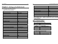
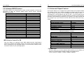
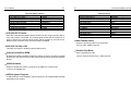
Specification:
TABLE OF CONTENTS
Model
ENDAT-3405M
Form Factor
System Chipset
Mini-ITX 170 mm x 170 mm (6.69”x6.69”) with 6 layers PCB
CPU Supporting
Memory
Ethernet
VGA
LCD interface
Duo View
Video Interface
Serial / Parallel
RS-422/485
Watchdog Timer
IDE Connector
SATA Connector
AUDIO
Expansion Slot
I/O Port
Digital IO
USB Port
Power Supply
The ENDAT-3405M System Board
VIA LUKE (NB+CPU) + VIA VT8237R Plus (SB)
Supports 133MHz FSB by VIA Luke integrated Eden-N
533MHz/800MHz/1.0GHz
1 x 184 pin DDR socket support DDR 400/333/266 up to 1GB
CHAPTER 1. INTRODUCTION ....................................................... 1
1-1.
1-2.
1-3.
1-4.
FEATURES .............................................................................................. 2
UNPACKING ............................................................................................ 3
ELECTROSTATIC DISCHARGE PRECAUTIONS ................................... 3
MOTHERBOARD LAYOUT ...................................................................... 4
VT8237R Plus integrated 10/100 Fast Ethernet w/ VT6103 (PHY)
Integrated VIA UniChrome™ Pro 3D/2D Graphics with SMA 16/32/64MB
24+24 (Option 18+18) bits w/ VT1631L
(dual channel LVDS Transmitter) (Optional w/ TTL LCD)
CRT+LCD
MPEG-4 & MPEG-2 Hardware decoding
(MPEG-4 only available on LUKE)
Hardware Rotation engine
4 Serial Port w/+5V, +12V Power Selector / 2 Parallel port
Via COM2 (Optional)
Programmable WDT from 1 to 255 seconds / minutes by
Winbond W83697HF
2 x 40pin IDE connector support UDMA 33/66/100/133,
1 x 44pin connector support Slim type HDD (share to IDE2)
2 x 150MB/s SATA device support Raid 0, 1, JBOD
Integrated VT8237R Plus Audio controller
w/ VT1612A Audio Codec for 2 Channel output
1x slim PCI slot up to 3 PCI slots via riser card with PCI 2.2 compliance
PS/2 Keyboard / Mouse Connector
2 x USB (2.0) + RJ-45 Connector w/LED indicator
D-sub Connector for COM 1, 2, 3
(internal box header for COM4) with POWER
1 x 25 Pins D-Sub Connector (LPT1)
1 D-Sub Connector and 1 internal box header (VGA)
1 IrDA TX/RX port with pin header
Box Header for COM4, TTL LCD, LVDS, CRT, LPT2
Pin Header for KB/MS, 4 x USB, CD-in, SPDIF-out,
Mic-in, Line-in, Line-out, SM Bus, KB/MS for external device
16-bits Digital I/O with CMOS/TTL level (8 bit input / 8 bit output)
6 x USB2.0 onboard
ATX power supply
CHAPTER 2. SETTING UP THE MOTHERBOARD ....................... 5
2-1. JUMPERS AND CONNECTORS.............................................................. 5
2-2. INSTALLING MEMORY.......................................................................... 16
2-3. SHARED VGA MEMORY ....................................................................... 16
2-4. INSTALLING RISER CARD.................................................................... 16
2-5. ASSIGNING IRQs FOR EXPANSION CARDS ....................................... 16
2-6. WATCHDOG TIMER…………………………………………………………. 17
2-7. DIGITAL I/O…………………………………………………………...………. 19
CHAPTER 3. AWARD BIOS SETUP............................................. 21
3-1. STANDARD CMOS FEATURES............................................................. 22
3-2. ADVANCED BIOS FEATURES............................................................... 23
3-3. ADVANCED CHIPSET FEATURES ........................................................ 24
3-4. INTEGRATED PERIPHERALS............................................................... 27
3-5. POWER MANAGEMENT SETUP........................................................... 31
3-6. PnP/PCI CONFIGURATIONS................................................................. 34
3-7. PC HEALTH STATUS ............................................................................. 35
3-8. FREQUENCY/VOLTAGE CONTROL ..................................................... 36
User’s Manual
V
CHPATER 4. VGA, LCD, FEATURE.............................................. 37
4-1. VGA FEATURE....................................................................................... 37
4-2. LVDS PANEL FEATURE......................................................................... 38
4-3. PCI BUS AUDIO ADAPTER FEATURES................................................ 39
4-4. DRIVER UTILITY INSTALLATION GUIDE ............................................. 40
CHPATER 5. LAN ADAPTER ........................................................ 42
5-1. FEATURES ............................................................................................ 42
5-2. UTP CABLE/RJ-45 JACK DEFINITION .................................................. 43
5-3. CONNECTING 100BASE-TX FAST ETHERNET NETWORK ................ 44
5-4. CONNECTING 10BASE-T ETHERNET NETWORK .............................. 44
5-5. 10MBASE/ 100MBASE INSTALLATION NOTICE .................................. 44
5-6. REMOTE BOOT ROM FUNCTION ........................................................ 45
5-7. LED INDICATORS.................................................................................. 45
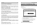
APPENDIX A: FLASH MEMORY UTILITY.................................... 46
APPENDIX B: CONNECTOR PIN ASSIGNMENT ........................ 47
APPENDIX C: LIMITED WARRANTY ........................................... 48
User’s Manual
1
Chapter 1. Introduction
ENDAT-3405M supports high performance processor of VIA Luke CoreFusion. It
also supports high speed DDR memory with 64-bit wide interfaces with non-ECC
DIMM (up to 1GB). Only Double Data Rate (DDR) SDRAM memory is supported
and the speed of memory can be 200, 266, 333 and 400 MHz.
ENDAT-3405M provides an integrated graphics (S3 Graphics UniChrome™ Pro
IGP) accelerator delivering cost competitive 3D, 2D, and video capabilities.
In addition to the integrated S3 Graphics UniChrome™ Pro IGP, featuring a 2D/3D
AGP8X graphics core with integrated MPEG-2 decoding and MPEG-4 acceleration
for smooth DVD and digital video playback, the VIA 'Luke' CoreFusion processing
platform also features support for high bandwidth DDR 333/400 memory, motion
compensation and DuoView for the latest multiple format flat panel display devices.
ENDAT-3405M with native dual channel Serial ATA/RAID controller provides direct
support for two 150MB/s Serial ATA devices. The V-RAID controller features native
RAID 0, RAID 1 and JBOD support, ensuring optimum data integrity and system
performance. The user-friendly V-RAID software interface enables easy disk array
configuration and management.
ENDAT-3405M supports IEEE 802.3 compliant 10 / 100 Mbps PCI bus master
Ethernet MAC with standard MII interface to external PHYceiver.
The ideal solution of ENDAT-3405M
- POS system
- KIOSK
- Interactive system
- Airport Terminal Controller
- Industrial controller
- Digital entertainment
- Embedded system equipment
2
The ENDAT-3405M System Board
1-1. Features
Basic Feature:
z
z
z
z
z
z
z
z
z
z
z
z
z
Board format: Mini-ITX (170mm x 170 mm)
Supports 133/100 MHz FSB by VIA Luke integrated Eden-N
533MHz/800MHz/1.0GHz
Digital I/O: 8 bits input and 8 bits output (3.3V)
Supports DDR 200/266/333/400 SDRAM up to 1GB
Serial ATA connector x 2
Enhance IDE connector x 2
Multiple I/O ports: COM port x 4; LPT port x 2; USB (2.0) x 6
All COM ports with +5V, +12V power selector
Watchdog Timer
VIA 10/100 LAN and Audio function onboard
With Intel embedded ATX PCI expansion design
On board chip provides LVDS interface (18/24/36/48 bit, single/dual
channels)
Support ATX Power Supply.
Optional features:
z
z
z
18 + 18 bits LVDS Transmitter
RS 422/485 via COM 2
Barebones system: niche into Unicorn U-6000 and U-8000 Chassis
Full Software Support:
z Drivers for major operating systems and APIs: Windows 9x / ME,
Windows 2000, Windows XP, Direct3D, DirectDraw and DirectShow,
OpenGL ICD for Windows 9x, and 2000, and DXVA for Windows
2000 and Windows XP
User’s Manual
3
1-2. Unpacking
The motherboard comes securely packaged in a sturdy cardboard shipping carton.
In addition to the User's Manual, the motherboard package includes the following
items:
ENDAT-3405M System Board
HDD / IO Cables
CDROM Driver includes: Drivers for Windows 98, ME, 2000, XP and AMI/AWARD
FLASH ROM utilities.
If any of these items are missing or damage, please contact the dealer from whom
you purchase the motherboard. Save the shipping material and carton in the event
that you want to ship or store the board in the future.
Note: Please leave the motherboard in its original package until you are ready to
install it!
1-3. Electrostatic Discharge Precautions
Make sure you properly ground yourself before handling the motherboard, or other
system components. Electrostatic discharge can easily damage the components.
Note: You must take special precaution when handling the motherboard in dry or
air-conditioned environments.
4
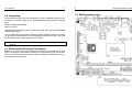
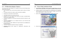
1-4. Motherboard Layout
The ENDAT-3405M System Board
5
User’s Manual
Chapter 2. Setting up the Motherboard
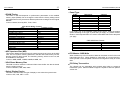
2-1. Jumpers and Connectors
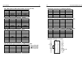
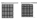
Jumpers/Connectors Overview:
Function
ATX Power Connector
Cooling Fan Connector
Buzzer
Battery
Clear CMOS
LCD Panel Connector
LVDS Panel Connector
LVDS Clock Selector
LVDS Voltage Selector
PS/2 MS/KB Box Header
PS/2 MS/KB Connector
OEM MS/KB Header
USB Port
Header for Case Panel
HDD active LED
External Speaker
Buzzer On/Off
Hardware Reset Switch
ATX Power Supply On/Off Switch
Power LED
WDT Function Enable/Disable
DDR SDRAM socket
LAN Connector
CRT Output
CRT Box Header
IR Box Header
COM1
COM2, COM3
COM4 Box Header
COM Port Voltage Selector
RS232 / 422/ 485 Selector for COM2
Jumpers/Connectors
ATXPWR
FAN1, FAN2
BUZZ1
BAT1
JBAT1
LCD1
LVDS1
JP1
JP2
CN1
JKBMS1
CN2
CN3, JUSB1, JUSB2
JP4
JP4: Pin 1(-), Pin 2(+)
JP4: Pin 3, Pin 6
JP4: Pin 4, Pin 5
JP4: Pin 7, Pin 8
JP4: Pin 9, Pin 10
JP4: Pin 11(-), Pin 12(+)
JP4: Pin 13, Pin 14
DIMM1
CN3
CN5
CN6
JP3
COM1
CN7
CN9
JP9
JP5 & JP6
6
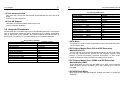
The ENDAT-3405M System Board
Function
IDE 1, IDE 2
SATA 1, SATA 2
SMBus
DIGITAL I/O Box Header
LPT1, LPT2
LINE OUT Connector
CD In Box Header
MIC IN / LINE IN Box Header
SPDIF Box Header
DIMM Power LED
System Power LED
Jumpers/Connectors
IDE1, IDE2, IDE2B1
SATA1, SATA2
JP7
JP8
LPT1, LPT2
CN10
JP10
JP11
SPDIF1
LED1
LED2
Please double-check the insertion and orientation of the LCD cable
before applying power. Improper installation will result in permanent
damage LCD panel.
Part 1: Onboard Jumpers
JBAT1: CMOS Data Clear (2.0mm)
Pin 1-2
Normal (Default)
Pin 2-3
Close for clear CMOS
JP1: LVDS Clock Selector (2.0mm)
Pin 1-3 *
Single-ended (Default)
Pin 2-4 *
Falling edge clock
Pin 3-5
Differential clock
Pin 4-6
Rising edge clock
JP2: LVDS Voltage Selector (2.0mm)
Pin-1, 2 *
+3.3V
Pin-3, 4
+5V
Pin-5, 6
+12V
Caution: Improper setting will damage LCD panel.
7
User’s Manual
JP4: Box Header for Case Panel (2.54mm)
Pin No.
Function
1(-), 2(+)
HDD active LED
3,6
External Speaker
4,5
Buzzer On/Off
7,8
Hardware Reset Switch
9,10
ATX Power On/Off
11(-),12(+)
Power LED
13,14
Close: Enable WDT function
JP5, JP6: RS232 / 422 / 485 Selector for COM2 (2.0mm)
TYPE
JP6 (3x4/2mm)
JP5 (2x7/2mm)
1-2, 4-5, 7-8, 10-11
1-2
RS-232 *
2-3, 5-6, 8-9, 11-12
3-4
RS-422
2-3, 5-6, 8-9, 11-12
5-6
RS-485
JP9: COM Port Voltage Selector (2.0mm)
Voltage
+12V(DC)
R.I. *
COM1 (JP9)
1-2
3-4
COM2 (JP9)
7-8
9-10
COM3 (JP9)
13-14
15-16
COM4 (JP9)
19-20
21-22
+5V(DC)
5-6
11-12
17-18
23-24
Part 2: Onboard Connectors
JP3: IR Box Header Connector (2.54mm)
Pin No.
Function
Pin No.
1
VCC
4
2
N.C
5
3
IRRX
JP7: SM Bus
Pin No.
1
2
Function
SMBCK
SMBDT
Pin No.
3
4
Function
GND
IRTX
Function
+3.3V
GND
8
The ENDAT-3405M System Board
JP8: DIGITAL I/O Box Header Connector (2.0mm)
Pin No.
Function
Pin No.
Function
1
+5V
2
+5V
3
DIO-O0
4
DIO-I0
5
DIO-O1
6
DIO-I1
7
DIO-O2
8
DIO-I2
9
DIO-O3
10
DIO-I3
11
DIO-O4
12
DIO-I4
13
DIO-O5
14
DIO-I5
15
GND
16
GND
17
DIO-O6
18
DIO-I6
19
DIO-O7
20
DIO-I7
21
+12V
22
+12V
JP10: CD IN Box Header Connector (2.54mm)
Pin No.
Function
Pin No.
Function
LO_J_R
CDL
1
2
GND_AUD
CDGND
3
4
GND_AUD
CDGND
5
6
LO_J_L
CDR
7
8
JP11: Microphone IN & LINE IN (2.54mm)
Pin No.
Function
Pin No.
Function
LINE_R
MIC POWER
1
2
GND
GND
3
4
GND
GND
5
6
LINE_L
MIC IN
7
8
SPDIF1: SPDIF Box Header Connector (2.0mm)
Pin No.
Function
+5V
1
N.C.
2
SPDIFOUT
3
GND
4
User’s Manual
9
10
The ENDAT-3405M System Board
CN1: PS/2 Keyboard / Mouse Box Header Connector (2.0mm)
Pin No. Signal (KB)
Pin No.
Signal (MS)
1
KB Data
2
MS Data
3
KEY
4
KEY
5
GND
6
GND
7
+5V(DC)
8
+5V(DC)
9
KB_CLK
10
MS_CLK
D-SUB Type Connector for COM2 port (RS-232)
Pin No. Description
Pin No.
Description
DCD
DSR
1
6
RXD
RTS
2
7
TXD
CTS
3
8
DTR
RI
4
9
GND
5
CN2: Pin Header for external device (2.0mm)
Pin No. Signal (KB)
Pin No.
Signal (MS)
KB Data Out
MS Data Out
1
2
KB Data In
MS Data In
3
4
KB CK Out
MS Data Out
5
6
KB CK In
MS CK In
7
8
KEY
KEY
9
10
+5V(DC)
+5V(DC)
11
12
GND
GND
13
14
D-SUB Type Connector for COM2 port (RS-422Æ 4 Wire)
Pin No.
Function
Pin No.
Function
–TXD
NA
1
6
+RXD
NA
2
7
+TXD
NA
3
8
NA
–RXD
4
9
NA
5
CN6: CRT Box Header Connector (2.0mm)
Pin No. Description
Pin No.
Description
RED
N.C / +5V
1
9
GREEN
GND
2
10
BLUE
N.C.
3
11
N.C.
DDC DAT
4
12
GND
H-Sync
5
13
GND
V-Sync
6
14
GND
DDC CLK
7
15
GND
8
CN9: Box Header Type Connector for COM4 port (RS-232)
Pin No.
Function
Pin No.
Function
DCD
DSR
1
6
RXD
RTS
2
7
TXD
CTS
3
8
DTR
RI
4
9
GND
N.C.
5
10
D-SUB Type Connector for COM2 port (RS-485Æ 2 Wire)
Pin No.
Function
Pin No.
Function
Data –
NA
1
6
NA
NA
2
7
Data +
NA
3
8
NA
NA
4
9
NA
5
ATXPWR: ATX Power connector
ATX
3.3V
11
1
3.3V
–12V
12
2
3.3V
GND
13
3
GND
PS ON
14
4
+5V
GND
15
5
GND
GND
16
6
+5V
GND
17
7
GND
–5V
18
8
POWER OK
+5V
19
9
5V SB
+5V
20
10
+12V
User’s Manual
LPT2: Printer (LPT2) Port Box Header (2.0mm)
Pin No. Description
Pin No.
Description
STB#
ACK#
1
10
PD0
BUSY
2
11
PD1
PE
3
12
PD2
SLCT
4
13
PD3
AFD#
5
14
PD4
ERR#
6
15
PD5
INIT#
7
16
PD6
SLIN#
8
17
9
PD7
18-25
GND
JUSB1 JUSB2: Box Header Type Connector for USB port (2.54mm)
Pin No.
Function
Pin No.
Function
1
USB_VCC
2
USB_VCC
3
USBD2-/44
USBD3-/55
USBD2+/4+
6
USBD3+/5+
7
USB_GND
8
USB_GND
9
USB_GND
10
USB_GND
FAN1, FAN2: CPU / 2nd Cooling Fan Connector
Pin No.
Function
GND
1
+12V
2
Sensor Pin
3
11
12
IDE1, IDE2: IDE1, IDE2 Connector
Pin No. Description
Pin No.
IDE Reset#
1
2
IDE data7
3
4
IDE data6
5
6
IDE data5
7
8
IDE data4
9
10
IDE data3
11
12
IDE data2
13
14
IDE data1
15
16
17
IDE data0
18
19
GND
20
21
IDE REQ
22
IDE IOW#
23
24
IDE IOR#
25
26
IDE Ready
27
28
IDE ACK#
29
30
IDE IRQ
31
32
IDE A1
33
34
IDE A0
35
36
IDECS1#
37
38
HDLED#
39
40
The ENDAT-3405M System Board
Description
GND
IDE data8
IDE data9
IDE data10
IDE data11
IDE data12
IDE data13
IDE data14
IDE data15
N.C.
GND
GND
GND
GND
GND
N.C.
P66DET
IDE A2
IDESC3#
GND
13
User’s Manual
IDE2B1: Slim IDE2 Connector (44Pins with 2.0mm)
Pin No.
1
3
5
7
9
11
13
15
17
19
21
23
25
27
29
31
33
35
37
39
41
43
Description
IDE Reset#
IDE data7
IDE data6
IDE data5
IDE data4
IDE data3
IDE data2
IDE data1
IDE data0
GND
IDE REQ
IDE IOW#
IDE IOR#
IDE Ready
IDE ACK#
IDE IRQ
IDE A1
IDE A0
IDECS1#
HDLED#
VCC(+5V)
GND
Pin No.
2
4
6
8
10
12
14
16
18
20
22
24
26
28
30
32
34
36
38
40
42
44
Description
GND
IDE data8
IDE data9
IDE data10
IDE data11
IDE data12
IDE data13
IDE data14
IDE data15
N.C.
GND
GND
GND
GND
GND
N.C.
P66DET
IDE A2
IDESC3#
GND
VCC(+5V)
N.C.
14
The ENDAT-3405M System Board
LCD1: LCD Panel Connector (2.0mm)
Pin No.
Signal
Pin No.
Signal
1
VBL
2
VBL
3
GND
4
GND
5
LCD-PWR
6
LCD-PWR
7
ENBKLT
8
GND
9
B0
10
B1
11
B2
12
B3
13
B4
14
B5
15
B6
16
B7
17
G0
18
G1
19
G2
20
G3
21
G4
22
G5
23
G6
24
G7
25
R0
26
R1
27
R2
28
R3
29
R4
30
R5
31
R6
32
R7
33
GND
34
GND
35
PCLK
36
PVS
37
PDE
38
PHS
39
GND
40
LCD-PWR
41
LCD-PWR
42
KEY
43
LCD-PWR
44
LCD-PWR
Please make sure the Pin 1 location before inserting the LCD connector.
15
User’s Manual
LVDS1: Dual LVDS Channel (2.0mm)
Pin No.
1
3
5
7
9
11
13
15
17
19
21
23
25
27
29
31
33
35
37
39
Signal
VBL (+12V)
GND
DISP.ON/OFF
LCD Power
GND
TxO0+
TxO1+
TxO2+
TxO3+
TxOC+
GND
TxE0+
TxE1+
TxE2+
TxE3+
TxEC+
LCD Power
GND
GND
VBL (+12V)
Pin No.
2
4
6
8
10
12
14
16
18
20
22
24
26
28
30
32
34
36
38
40
16
The ENDAT-3405M System Board
2-2. Installing Memory
Signal
VBL (+12V)
GND
GND
LCD Power
GND
TxO0TxO1TxO2TxO3TxOCKEY
TxE0TxE1TxE2TxE3TxECLCD Power
GND
GND
VBL (+12V)
ENDAT-3405M system board offers one 184pin DDR SDRAM socket supports up to
1GB memory and the speed can be 200/266/333/400 MHz.
2-3. Shared VGA Memory
ENDAT-3405M is using built-in AGP VGA controller with S3 Graphics UniChrome
Pro IGP graphics core up to 64MB of system memory. The amount of video
memory on motherboard determines the number of colors and the video graphic
resolution.
2-4. Installing Riser Card
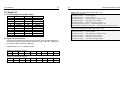
Installing Riser Card (Max. 3 PCI Slots on Riser Card)
PCI Slot
INT
ADSEL
PCI 1 A,B,C,D
AD24
PCI 2 B,C,D,A
AD23
PCI 3 C,D,A,B
AD22
PCI 4 D,A,B,C
AD21
The default INT/AD-select for ENDAT-3405M All-In-One motherboard is listed in the
above table.
Please make sure the Pin 1 location before inserting the LVDS connector.
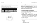
2-5. Assigning IRQs for Expansion Cards
LVDS Panel ID:
ID No.
0
1
2
3
4
5
6
7
Resolution
640 x 480
800 x 600
1024 x 768
1280 x 768
1280 x 1024
1400 x 1050
1600 x 1200
1366 x 768<Optional>
Channel
1
1
1
1
2
2
2
1
Some expansion cards require an IRQ (Interrupt request vector) to operate.
Generally, each IRQ must be exclusively assigned to specific use. In a standard
design, there are 16 IRQ available with 11 of them already in used by other part of
the system.
Some PCI expansion cards need IRQ; any remaining IRQ could be assigned to PCI
Bus. Microsoft's Diagnostic (MSD.EXE) utility included in the Windows directory
can be used to see their map. Clients can not have more than one device apply the
same IRQ in the system or it will cause the system hang up, crash, and unexpected
results. To simplify the process, this motherboard complies with the Plug and Play
(PnP) specifications, which was developed to allow automatic system configuration.
Whenever a PnP-compliant card is added to the system, PnP card and IRQs will
automatically assigned if available. The PCI and PnP configuration in the BIOS
setup utility can indicate which IRQs have being used by Legacy cards.
17
User’s Manual
In the PCI Bus design, the BIOS is automatically assigned an IRQ to a PCI slot that
has a card in it which requires an IRQ. To install PCI cards via riser card, you need
to set the correct "ADSEL" and "INT" (interrupt) assignment on the jumper of riser
card.
IRQ
0
1
2
3
4
5
6
7
8
9
10
11
12
13
14
15
Status
Used
Used
Used
Used
Used
Used
Used
Used
Used
Used
Used
Used
Used
Used
Used
Used
Assignment
Timer
Keyboard
Second 8259
COM 2
COM 1
LPT 2
Floppy Disk
LPT 1
RTC Alarm
IRQ2 Redir
Reserved
Reserved
PS/2 Mouse
Coprocessor
Hard Disk (IDE 1)
Reserved (IDE 2)
2-6. Watchdog Timer
Watchdog Timer (WDT) is a special design for system monitoring to secure the
system work normally. WDT has an independent clock from the oscillator and could
set time and clear/refresh WDT counter function. When time is up, WDT will send
hardware RESET signal to reset system.
Timeout Value Range
-1 to 255
-Second or Minute
18
The ENDAT-3405M System Board
Program Sample
#include <stdio.h>
#include <dos.h>
#include <dir.h>
void show_ver();
void main()
{
unsigned int tt;
clrscr();
show_ver();
tt=0;
while((tt==0)||(tt>255))
{
printf("\n\nPlease key in how many seconds you want to reset system
(1~255):");
scanf("%d",&tt);
}
outportb(0x2e,0x87); //Unlock register
outportb(0x2e,0x87); //Unlock register
outportb(0x2e,0x07); //Set Logic Device number pointer
outportb(0x2f,0x08); //Set Logic Device number
outportb(0x2e,0x29); //set active reg is cr29
outportb(0x2f,0x20); //set reg value Pin119 Fun (bit5:6=01 WDTO)
outportb(0x2e,0x30); //set active reg is CR30
outportb(0x2f,0x01); //set reg value MIDI & GP5 active (bit0 =1 active,0
inactive )
outportb(0x2e,0xf3); //Set active register is CRF3
outportb(0x2f,0x00); //Set register value (bit2=1: minute. =0: second)
outportb(0x2e,0xf4); //Set active register is CRF4
outportb(0x2f,tt);
//Set time out value of WDT
}
void show_ver()
{
unsigned char tmp0;
printf("Designed by ROBERT LIOU of UNICORN computer corp.
\n2005/10/07 release version:1.0a\n");
printf("This program is design for test Watch Dog Timer for
ENADT-3405M(W83697HF).\n");
}
19
User’s Manual
Function
+5V
DIO-O0
DIO-O1
DIO-O2
DIO-O3
DIO-O4
DIO-O5
GND
DIO-O6
DIO-O7
+12V
Pin No.
2
4
6
8
10
12
14
16
18
20
22
The ENDAT-3405M System Board
Sample code for input (using Turbo C/C++ 3.0):
#define input_port 0x2f
outportb(0x4e,0x87); //Unlock register
outportb(0x4e,0x87); //Unlock register
outportb(0x4e,0x07); //Set Logic Device number pointer
outportb(0x4f,0x09); //Set Logic Device number
outportb(0x4e,0xF1); //Set active register is CRF1
read_data=inportb(input_port); // Read digital input data
printf("DIO-Input=%02X\n",read_data); //Show digital input data on screen
2-7. Digital I/O
1) Pin out of digital I/O header (JP8):
Pin No.
1
3
5
7
9
11
13
15
17
19
21
20
Function
+5V
DIO-I0
DIO-I1
DIO-I2
DIO-I3
DIO-I4
DIO-I5
GND
DIO-I6
DIO-I7
+12V
Sample code for Output (using Turbo C/C++ 3.0):
outportb(0x4e,0x87); //Unlock register
outportb(0x4e,0x87); //Unlock register
outportb(0x4e,0x07); //Set Logic Device number pointer
outportb(0x4f,0x09); //Set Logic Device number
outportb(0x4e,0xF4); //Set active register is CRF4
outportb(0x4f,0xFF); // Write data to digital output
2) Digital I/O port address:
This function is support by onboard super I/O chip; it can be control easily by
change the register of super I/O chip via I/O port “4Eh” and “4Fh”. Please see
the sample code of below for implement.
Voltage tolerance: +/- 5% with 0V to +5V.
Register configuration (input):
7
6
5
Bit No
IN7
IN6
IN5
Map
4
IN4
3
IN3
2
IN2
1
IN1
0
IN0
Register configuration (output):
Bit No
7
6
5
Map
OUT7 OUT6 OUT5
4
OUT4
3
OUT3
2
OUT2
1
OUT1
0
OUT0
21
User’s Manual
Chapter 3. AWARD BIOS SETUP
22
The ENDAT-3405M System Board
3-1. Standard CMOS Features
The Standard Setup is used for the basic hardware system configuration. The main
function is for Data/Time and Hard Disk Drive settings.
Phoenix – Award BIOS CMOS Setup Utility
> Standard CMOS Features
> Advanced BIOS Features
> Advanced Chipset Features
> Integrated Peripherals
> Power Management Setup
> PnP/PCI Configurations
> PC Health Status
> Frequency/Voltage Control
Load Optimized Defaults
Set Supervisor Password
Set User Password
Save & Exit Setup
Exit Without Saving
Use the CMOS setup program to modify the system parameters to reflect the
environment installed in your system and to customize the system as desired.
Press the <DEL> key to enter into the CMOS setup program when you turn on the
power. Settings can be accessed via arrow keys. Press <Enter> to choose an
option to configure the system properly.
In the main menu, press F10 or “SAVE & EXIT SETUP” to save your changes and
reboot the system. Choose “EXIT WITHOUT SAVING” to ignore the changes and
exit the setup procedure. Pressing <ESC> at anywhere during the setup will return
to the main menu.
“Advanced BIOS Features”, “Advanced Chipset Features” and “PnP/PCI
Configurations” requires board knowledge on PC/AT system architecture and Intel
chipset specification. Incorrect setup could cause system malfunctions.
Item
Date (mm:dd:yy)
Time (hh:mm:ss)
IDE Channel 0 Master:
IDE Channel 0 Slave :
IDE Channel 1 Master:
IDE Channel 1 Slave :
IDE Channel 2 Master :
IDE Channel 3 Master :
Video
Halt On
Available Options:
Auto
Auto
Auto
Auto
Auto
Auto
EGA/VGA
All , But Keyboard
․Video
Select the type of primary video subsystem.
<Choice: EGA / VGA, CGA 40, CGA 80, MONO>
․Halt On
Set the system’s response to specific boot errors.
<Choice: All Errors, No Errors, All, But Keyboard>
IDE Drives
Item
IDE HDD Auto-Detection
IDE Channel
Access Mode
Available Options:
Press Enter
Auto
Auto
The specifications of your drive must match with the drive table. The hard disk will
not work properly if you enter incorrect information in this category. Select “Auto”
whenever possible. If you select “Manual”, make sure the information is from your
hard disk vendor or system manufacturer.
User’s Manual
23
3-2. Advanced BIOS Features
This section allows you configuring your system for basic operation. You have the
opportunity to select the system’s default speed, boot-up priority, keyboard
operation and security.
Item
Available Options:
Hard Disk Boot Priority
Press Enter
Virus Warning
Disabled
CPU Internal Cache
Enabled
External Cache
Enabled
CPU L2 Cache ECC Checking
Enabled
Processor Number Feature
Enabled
Quick Power On Self Test
Enabled
First Boot Device
CDROM
Second Boot Device
Hard Disk
Third Boot Device
LS120
Boot Other Device
Enabled
Boot Up NumLock Status
On
Typematic Rate Setting
Disabled
Typematic Rate (Chars/Sec)
6
Typematic Delay (Msec)
250
Security Option
Setup
MPS Version Control For OS
1.4
OS Select For DRAM > 64MB
Non-OS2
Video BIOS Shadow
Enabled
Small Logo(EPA) Show
Enabled
․MPS Version Control For OS
This item allows you selecting which MPS (Multi-Processor Specification)
version to be used for the operating system. You need to select the MPS version
that is supported by your operating system. To find out which version to use,
consult the vendor of your operating system.
24
The ENDAT-3405M System Board
3-3. Advanced Chipset Features
This section allows you to configure the system based on the specific features of
the installed chipset. This chipset manages bus speeds and the access to the
system memory resources, such as DRAM and the external cache. It also
coordinates the communications with the PCI bus. It must be stated that these
items should never be altered. The default settings have been chosen because they
provide the best operating conditions for your system. You might consider making
any changes only if you discover that the data has been lost while using your
system.
Item
DRAM Clock/Drive Control
AGP & P2P Bridge Control
CPU & PCI Bus Control
Memory Hole
System BIOS Cacheable
Video RAM Cacheable
Init Display First
Available Options:
Press Enter
Press Enter
Press Enter
Disabled
Enabled
Disabled
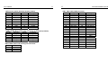
PCI Slot
DRAM Clock/Drive Control
Item
Current FSB Frequency
Current DRAM Frequency
DRAM Clock
DRAM Timing
SDRAM CAS Latency
Bank Interleave
Precharge to Active(Trp)
Active to Precharge(Tras)
Active to CMD(Trcd)
REF to ACT/REF to REF(Trfc)
ACT(0) to ACT(1) (TRRD)
DRAM Command Rate
Available Options:
133MHz
166MHz
By SPD
Auto By SPD
2.5
Disabled
4T
9T
4T
15T
3T
2T Command
․DRAM Clock
This item allows you to set the speed of Direct Memory Access (DMA) at either
equal to or one-half of the SYSCLK (system clock signal) speed.
<Choice: By SPD, 100MHz, 133MHz, 166MHz, 200MHz>
25
User’s Manual
26
The ENDAT-3405M System Board
․Panel Type
․DRAM Timing
The value in this field depends on performance parameters of the installed
memory chips (DRAM). Do not change the value from the factory setting unless
you install new memory that has a different performance rating than the original
DRAMs.
<Choice: Manual, Auto By SPD, Turbo, Ultra>
AGP & P2P Bridge Control
Item
AGP Aperture Size
AGP 3.0 Mode
AGP Driving Control
AGP Driving Value
AGP Fast Write
AGP Master 1 WS Write
AGP Master 1 WS Read
AGP 3.0 Calibration Cycle
VGA Share Memory Size
Direct Frame Buffer
Select Display Device
Panel Type
Available Options:
128M
8X
Auto
DA
Enabled
Disabled
Disabled
Disabled
64M
Enabled
CRT
07
ID No.
0
1
2
3
4
5
6
7
Resolution
640 x 480
800 x 600
1024 x 768
1280 x 768
1280 x 1024
1400 x 1050
1600 x 1200
1366 x 768<Optional>
Channel
1
1
1
1
2
2
2
1
If you apply one of the standard panels shown above, select the appropriate
option according to the type of panel that you apply. Or, please contact your
dealer or sales representative for custom-made BIOS that will suit the panel that
you apply.
CPU & PCI Bus Control
Item
PCI Master 0 WS Write
PCI Delay Transaction
VLink mode selection
VLink 8X Support
Available Options:
Enabled
Enabled
Mode 1
Enabled
․AGP Aperture Size (MB)
This function determines the amount of system memory that is given to the AGP
card. This is a dynamic memory allotment in that the AGP card will only use the
amount of memory that it needs. The remaining memory, which is not in use, will
be available for the system.
<Choice: 32MB, 64MB, 128MB, 256MB, 512MB, 1G>
․VGA Share Memory Size
This field is used to select the onboard VGA’s frame buffer size that is shared
from the system memory.
<Choice: Disabled, 16M, 32M, 64M>
․Select Display Device
This field is used to select the type of display to use when the system boots.
<Choice: CRT, LCD, CRT + LCD>
․PCI Master 0 WS Write
When enabled, up to four D words of data can be written to the PCI bus without
interrupting the CPU. When disabled, a write buffer is not used and the CPU
read cycle will not be completed until the PCI bus signals is ready to receive the
data.
․PCI Delay Transaction
The chipset has an embedded 32-bit posted write buffer to support delay
transaction cycles. Select Enabled to support compliance with PCI specification
version 2.2.
27
User’s Manual
28
The ENDAT-3405M System Board
VIA OnChip IDE Device
․V-Link mode selection
This menu item controls the data transfer speed between the north and south
bridge.
<Choice: By Auto, Mode 0~4>
․V-Link 8X Support
This setting controls the utilized widths of the V-link.
<Choice: Enabled, Disabled>
3-4. Integrated Peripherals
The IDE hard drive controllers support up to two separate hard drives. These drives
have a master/slave relationship that is determined by the cabling configuration
used to attach them to the controller. Your system supports two IDE controllers--a
primary and a secondary--so you can install up to four separate hard disks.
Integrated Peripherals
Item
VIA OnChip IDE Device
VIA OnChip PCI Device
SuperIO Device
Onboard Serial Port 3
Serial Port 3 Use IRQ
Onboard Serial Port 4
Serial Port 4 Use IRQ
Onboard Parallel Port 2
Parallel Port 2 Use IRQ
Parallel Port 2 Mode
LPT2 ECP Mode Use DMA
Available Options:
Press Enter
Press Enter
Press Enter
3E8
IRQ5
2E8
IRQ5
278
IRQ9
EPP1.9+SPP
3
Item
OnChip SATA
SATA Mode
OnChip IDE Channel0
OnChip IDE Channel1
IDE Prefetch Mode
Primary Master
PIO
Primary Slave
PIO
Secondary Master PIO
Secondary Slave
PIO
Primary Master
UDMA
Primary Slave
UDMA
Secondary Master UDMA
Secondary Slave
UDMA
IDE HDD Block Mode
Available Options:
Enabled
IDE
Enabled
Enabled
Enabled
Auto
Auto
Auto
Auto
Auto
Auto
Auto
Auto
Enabled
․SATA Mode
These fields are used to select the RAID/IDE mode of the serial ATA drives.
<Choice: RAID, IDE>
․IDE Primary Master/Slave PIO and IDE Secondary
Master/Slave PIO
The four IDE PIO (programmed Input/Output) fields let you set a PIO mode (0-4)
for each IDE device that the internal PCI IDE interface supports. Modes 0
through 4 provide successively increased performance. In Auto mode, the
system automatically determines the best mode for each device.
․IDE Primary Master/Slave UDMA and IDE Secondary
Master/Slave UDMA
These fields allow you to set the Ultra DMA in use. When Auto is selected, the
BIOS will select the best available option after checking your hard drive or
CD-ROM.
․IDE HDD Block Mode
Block mode is also called block transfer, multiple commands, or multiple sectors
read/write.
29
User’s Manual
30
The ENDAT-3405M System Board
VIA OnChip PCI Device
Item
VIA-3058 AC97 Audio
VIA-3043 OnChip LAN
Onboard LAN Boot ROM
OnChip USB Controller
OnChip EHCI Controller
USB Emulation
USB Keyboard Support
Available Options:
Enabled
Enabled
Disabled
All Enabled
Enabled
ON
Enabled
․VIA-3058 AC97 Audio
Allow the motherboard's BIOS to detect whether you are using any audio device.
If an audio device is detected, the onboard audio Codec will be enabled; if no
audio is detected, the onboard audio Codec will be disabled. If you want to use
different audio controller cards, set these fields to Disabled.
SuperIO Device
Item
Onboard Serial Port 1
Onboard Serial Port 2
UART Mode Select
RxD, TxD Acitve
IR Transmission Delay
UR2 Duplex Mode
Use IR Pins
Onboard Parallel Port
Parallel Port Mode
EPP Mode Select
ECP Mode Use DMA
Available Options:
3F8/IRQ4
2F8/IRQ3
Normal
Hi,Lo
Enabled
Half
IR-Rx2Tx2
378/IRQ7
SPP
EPP1.7
3
․UART Mode Select
Select an operating mode for the serial port.
․VIA-3043 OnChip LAN
<Choice: IrDA, ASKIR, Normal>
This field can enable or disable onboard LAN function.
․Parallel Port Mode
․Onboard LAN Boot ROM
By default, this field is disabled. Enable this field if you wish to use the boot ROM
(instead of a disk drive) to boot-up the system and access the local area network
directly.
․USB Emulation
Enable or disable the system’s support for the USB port in DOS mode.
<Choice: Off, KB/MS, On>
․USB Keyboard Support
If USB Emulation is set at KB/MS, this item allows you to enable/disable the USB
keyboard/mouse support.
Set the parallel port mode.
<Choice: SPP, EPP, ECP, ECP + EPP, Normal>
User’s Manual
31
3-5. Power Management Setup
The Power Management Setup allows users configuring the system to save energy
in a most effective way while operating in a manner consistent with their own style of
computer use.
Item
Available Options:
ACPI function
Enabled
ACPI Suspend Type
S1(POS)
Power Management Option
User Define
HDD Power Down
Disabled
Suspend Mode
Disabled
Video Off Option
Suspend -> Off
Video Off Method
V/H SYNC+Blank
Soft-Off by PWRBTN
Instant-Off
Run VGABIOS if S3 Resume
Auto
AC Loss Auto Restart
Off
Delay Prior to Thermal
16 Min
IRQ/Event Activity Detect
Press Enter
32
The ENDAT-3405M System Board
IRQ/Event Activity Detect
Item
PS2KB Wakeup Select
PS2KB Wakeup from S3/S4/S5
PS2MS Wakeup from S3/S4/S5
USB Resume from S3
VGA
LPT & COM
HDD & FDD
PCI Master
Wake Up By Internal LAN
Modem Ring Resume
RTC Alarm Resume
Date (of Month)
Resume Time (hh:mm:ss)
IRQs Activity Monitoring
Available Options:
Hot key
Disable
Disabled
Disabled
OFF
LPT/COM
ON
OFF
Disabled
Disabled
Disabled
0
0: 0: 0
Press Enter
․PS2KB Wakeup Select
․ACPI Function
This function should be enabled only in operating systems that support ACPI.
Currently, only Windows® 98SE/2000/ME/XP supports this function. When this
field is enabled, the system will ignore the settings in the “Suspend Mode” and
“HDD Power Down” fields. If you want to use the Suspend to RAM function,
make sure this field is enabled then select“S3 (STR)” in the field below.
․ACPI Suspend Type
This field is used to select the type of Suspend mode.
Enables the Power On Suspend function.
S1(POS)
Enables the Suspend to RAM function.
S3(STR)
If S3 state is supported by the system, by default [S3] is
S1 & S3
automatically selected. Otherwise [S1] is selected.
․Run VGABIOS if S3 Resume
Select whether to run VGA BIOS if resuming from S3 state. This is only
necessary for older VGA drivers.
<Choice: Auto, Yes, No>
When selecting “Password”, press <Enter> to change password. The maximum
number of characters is eight. “PS2KB Wakeup from S3/S4/S5” and “PS2MS
Wakeup from S3/S4/S5” will be disabled while changing the password.
<Choice: Hot Key, Password>
33
User’s Manual
IRQs Activity Monitoring
Item
Primary INTR
IRQ 3 (COM 2)
IRQ 4 (COM 1)
IRQ 5 (LPT 2)
IRQ 6 (Floppy Disk)
IRQ 7 (LPT 1)
IRQ 8 (RTC Alarm)
IRQ 9 (IRQ2 Redir)
IRQ 10 (Reserved)
IRQ 11 (Reserved)
IRQ 12 (PS/2 Mouse)
IRQ 13 (Coprocessor)
IRQ 14 (Hard Disk)
IRQ 15 (Reserved)
Available Options:
ON
Disabled
Enabled
Enabled
Enabled
Enabled
Disabled
Disabled
Disabled
Disabled
Enabled
Enabled
Enabled
Disabled
․Primary INTR
Restore the system to an active state if IRQ activity is detected from any of the
enabled channels.
34
The ENDAT-3405M System Board
3-6. PnP/PCI Configurations
This section describes the configuration of the PCI bus system. PCI is a system
that allows I/O device to operate at speeds nearing the speed of the CPU itself,
when communicating with its own special components. This section covers some
very technical items. It is strongly recommended that only experienced users make
any changes to the default settings.
Item
Available Options:
PNP OS Installed
No
Reset Configuration Data
Disabled
Resources Controlled By
Auto(ESCD)
IRQ Resources
Press Enter
IRQ-3 assigned to
PCI Device
IRQ-4 assigned to
PCI Device
IRQ-5 assigned to
PCI Device
IRQ-7 assigned to
PCI Device
IRQ-9 assigned to
PCI Device
IRQ-10 assigned to
PCI Device
IRQ-11 assigned to
PCI Device
IRQ-12 assigned to
PCI Device
IRQ-14 assigned to
PCI Device
IRQ-15 assigned to
PCI Device
PCI/VGA Palette Snoop
Disabled
Assign IRQ For VGA
Enabled
Assign IRQ For USB
Enabled
․Reset Configuration Data
Enabled
Disabled
The BIOS will reset the Extended System Configuration Data
(ESCD) once automatically. It will then recreate a new set of
configuration data.
The BIOS will not reset the configuration data.
․Reset Configuration Data
Auto(ESCD)
Manual
The system will automatically detect the settings for you.
Choose the specific IRQ in the “IRQ Resources” field.
35
User’s Manual
․PCI/VGA Palette Snoop
The ENDAT-3405M System Board
3-8. Frequency / Voltage Control
When set to [Enabled], multiple VGA devices operating on different buses can
handle data from the CPU on each set of palette registers on every video device.
Bit 5 of the command register in the PCI device configuration space is the VGA
Palette Snoop bit (0 is disabled).
3-7. PC Health Status
This screen shows the information of temperature, Fan speed and Vcore etc. It also
can set CPU warning temperature to protect CPU.
PC Health Status
Item
CPU Warning Temperature
Current System Temp.
Current CPU1 Temperature
Current CPUFan1 Speed
Current CPUFan2 Speed
Vcore
+3.3V
+5V
+12 V
VBAT (V)
5VSB (V)
Shutdown Temperature
36
Available Options:
Disabled
Frequency/Voltage Control
Item
VIA C3 Clock Ratio
Auto Detect PCI/DIMM Clk
Spread Spectrum
CPU Host/3V66/PCI Clock
Available Options:
Default
Enabled
Disabled
Default
․VIA C3 Clock Ratio
This item is for VIA C3 CPU Ratio adjustment.
․Auto Detect DIMM/PCI Clk
When enabled, the system will automatically send clock signals to existing PCI
devices.
․Spread Spectrum
Leave this field in its default setting. Do not alter this setting unless advised by an
engineer or technician.
Disabled
․CPU Warning Temperature
Select the combination of lower and upper limits for the CPU temperature, if your
computer contains an environmental monitoring system. If the CPU temperature
extends beyond either limit, any warning mechanism programmed into your
system is activated.
․Shutdown Temperature
Select the combination of lower and upper limits for the system shutdown
temperature, if your computer contains an environmental monitoring system. If
the temperature extends beyond either limit, the system shuts down.
User’s Manual
37
Chapter 4. VGA, LCD Feature
38
4-2.
The ENDAT-3405M System Board
LVDS Panel Feature
The on-board graphic controller supports industry standard LCD panel, LVDS
interface only, with 1 channel (18 or 24) and 2 channels (36 or 48bit) data width.
4-1.
VGA Feature
ENDAT-3405M provides integrated S3 Graphics UniChrome™ Pro IGP, featuring a
2D/3D AGP8X graphics core with integrated MPEG-2 decoding and MPEG-4
acceleration for smooth DVD and digital video playback, the VIA 'Luke' CoreFusion
processing platform also features support for high bandwidth DDR 333/400
memory, motion compensation and DuoView for the latest multiple format flat panel
display devices.
With an internal data flow equivalent to what is available to the latest AGP 8X
graphics cards, Unichrome Pro has separate 128-bit data path between the North
Bridge for pixel data flow and texture/command access. Separate 128-bit 2D and
3D graphics engines ensure optimal performance for all multimedia, entertainment,
and productivity applications.
Unichrome Pro includes native support for the most popular digital video and audio
playback through hardware MPEG-4/-2 acceleration and acclaimed VIA Vinyl Audio
suite, delivering spectacular playback for entertainment devices.
Unichrome Pro with its optimized shared memory architecture and high definition
video support through the Chromotion CE Video Display Engine offers a
breathtaking visual experience for the latest HDTV format displays.
The on-board Graphics Controller supports a full AGP implementation internally to
remain compatible with existing software and programming models. However,
since the engine is integrated, it enjoys a higher bandwidth and lower latency than
is possible with discrete solutions.
The controller of ENDAT-3405M supports 2 types of display: CRT and LVDS panel.
LVDS interface provides low voltage, high speed and low EMI serial DC-balanced
differential data via optional onboard LVDS.
The flat panel interface provides or supports following functions for various panels:
- Generates LVDS flat panel channels like clock and data channel.
- Generates different video data formats to directly drive different types of
panels (18, 24, 36 or 48bit)
- Wide screen resolution as 16:9 or 16:10.
- Vertical and horizontal expansion of video displays to LCD panel resolution
- Vertical and horizontal centering
- Panel power sequence
User’s Manual
4-3.
39
PCI Bus Audio Adapter Features
40
The ENDAT-3405M System Board
4-4.
Driver Utility Installation Guide
The Chipset built-in SoundBlaster Pro Hardware and Direct Sound Ready AC97’
Digital Audio Controller
5-
When finishing the installation of Windows platform (95/98/2000/NT), please install the
relative VIA driver (4in1) utilities for compliance compatibility of hardware environment.
•
6-
Insert the support CD that supplied with motherboard into CD-ROM driver
which enable the access with auto-run mode; or double –click the CD driver
icon in “My Computer” to bring up the screen.
7-
Select correct motherboard to install driver / utility for the system
8-
Select VIA 4in1 service pack driver install to the system
Dual full-duplex direct sound channels between system memory and AC97’
link
•
PCI Master interface with scatter / gather and bursting capability
•
32byte FIFO of each direct sound channel
•
Host based sample rate converter and mixer
•
Standard v1.0 or v2.0 AC98’ Codec interface for single or cascaded AC97’
Codec’s from multiple vendors
•
Loop back capability for re-directing mixed audio streams into USB and 1394
speakers
•
Hardware SoundBlaster Pro for Windows DOS box and real-mode DOS
legacy compatibility
•
Plug and Play with 4 IRQ, 4 DMA and 4 I/O space options for SoundBlaster Pro
and MIDI hardware
•
Hardware assisted FM synthesis for legacy compatibility
•
Complete software driver support for Windows-95, Windows-98 and
Windows-NT
User’s Manual
9-
41
The Screen will appear VIA 4in1 driver setup screen, please press “NEXT” to
continue. Please follow the steps instructed by each screen for the installation
of the VIA 4in1 driver. Restart the system after completed the installation.
10- After installing the VIA 4in1 driver, please select VGA driver for install. The
system will request for “restart” after the completion of the driver installation.
11- The Screen can be adjusted at Display properties after the installation of VGA
driver.
We strongly recommend using the 4in1 driver to install the system since the 4in1 driver will
automatically detect / update the necessary drivers.
This driver will automatically detect and install the latest utilities as following:
IDE Bus master, VIA AGP Driver, IRQ Routing Driver, VIA INF Driver
42
The ENDAT-3405M System Board
Chapter 5. LAN Adapter
The on-board LAN adapter integrated of Single Chip Fast Ethernet Controller with
options of one or dual LAN solution, and also the LAN chip option of VIA VT6103
solution. It is highly integrated and requires no “glue” logic external memory on
board. It runs in the bus master mode and directly sending/receiving Ethernet
packet to/from memory. The On-board LAN adapter can directly fetch the system
CPU. Also, it can transfer data Directly between I/O devices and system memory in
the 32-bit bus master mode that provides low CPU utilization.
It complies with the IEEE 802.3x standard, IEEE802.3 standard and PCI Local Bus
version 2.1 and transmits data on the network at 100 Mbps or 10 Mbps. It also
operates in full-duplex mode that doubles the network speed up to 20/200 Mbps
when working with Fast Switching Hub. Built-in one RJ-45 port for connection of
100Base-TX Fast Ethernet or 10Base-T Ethernet network, and automatically
senses the connection type.
LAN Driver: Install the LAN driver for on-board LAN adapter.
5-1. Features
VGA Driver: Install the VGA driver for on-board AGP VGA adapter
•
Full compliancy with PCI Rev. 2.1
•
Complies with the Ethernet/IEEE 802.3u 100Base-TX and 10 Base-T industry
standard
•
Supports full-duplex operations, thus doubling the network speed up to
20Mbps on 10 Base-T Ethernet or 200Mbps on 100 Base-TX Fast Ethernet
when setting in full duplex mode
•
Two LED indicators to report network status
•
One RJ-45 connector with Auto-sense cable type of 10 or 100Mbps network
operation
•
Supports PCI clock speed up to 33MHz, capable of zero wait states
•
Supports Remote Boot ROM by system BIOS
•
Provides a comprehensive setup program for displaying the adapter
configuration and includes diagnostic on board or network tests
•
Complete drivers for Novell, Windows NT and Windows 95/98 Packet driver etc
Please download or check from VIA Web site: www.via.com.tw if you prefer to install the drivers
individually or you need more information.
User’s Manual
43
44
The ENDAT-3405M System Board
5-2. UTP Cable / RJ-45 Jack Definition
5-3. Connecting 100Base-TX Fast Ethernet Network
Straight through twisted pair cable is typically used to connect a hub to a server or
workstation. In a straight through connection, Pin 1 at the server, Pin 2 at the hub
connects to Pin 2 at the server, and so on. Figure A-1 shows the locations of pins on
a standard RJ-45 plug on a twisted-pair cable.
The system board provides an RJ-45 port for connection to 100Base-TX Fast
Ethernet or 10Base-T Ethernet Network with a single connection over unshielded
twisted-pair (UTP). The adapter automatically operates at 10Mbps or 100Mbps
when the appropriate 10/100Base hub is connected.
Table A-1 shows the wiring in a straight-through twisted-pair cable (Pins 4, 5, 7 and
8 are not used).
Twisted Pair
Signal
Signal
Pin Number
To Pin Number
Number
Description
Description
1
TD+
1
TD+
Æ
1
2
TD–
2
TD–
3
RD+
3
RD+
Æ
2
6
RD–
6
RD–
To connect the adapter to 100Base-TX Fast Ethernet Network, you need a
twisted-pair Category 5 cable with RJ-45 modular jacks at both ends. This cable
can have a maximum length of 300 feet (100 meters).
RJ-45 Connector Pin Assignments
5-4. Connecting 10Base-T Ethernet Network
To connect the adapter to a 10Base-T Ethernet Network, you need a twisted-pair
Category 3, 4 or 5 cables with RJ-45 modular jacks at both ends. This cable can
have a maximum length of 300 feet (100 meters).
Figure A-1 shows the RJ-45 Connector pin assignments
5-5. 10MBase/100MBase Installation Notice
•
•
•
•
•
•
100Mbps network must be shielded twisted-pair (STP) or Category 5 unshielded
twisted-pair cable. Do not use a Category 3 or 4 cable for 100Mbps-network operation,
it could cause data loss. Category 3 or 4 cable is good for 10Mbps network only.
Category 5 cable is also good for 10Mbps operation. Use UTP Category 5 cable for
the versatility to operate the network at either 100Mbps or 10Mbps speed without
changing cable.
Two pairs of wiring are required.
Depending on building codes, different insulation materials may be required.
Plenum-rated or TEFLON-coated wiring maybe required in some areas where
fireproofing is required.
The wire gauge should be between 18 and 26 AWG (Most telephone installations use
24-gauge wiring).
UTP cable should meet the following requirements:
1. Solid copper
2. Nominal capacitance: less than 16pF/ft
3. Nominal impedance: 100 ohms
4. Nominal attenuation: less than 11.5db
User’s Manual
45
Automatic Selection of the Media Type
While the driver installs, it automatically detects the media type based on the type of
cable connected. Once you change the cable type, you must reinstall the driver to
execute auto-detect again.
If the driver cannot detect which cable is connected or whether a cable is
connected, look at cabling network driver (Ex. Modify net.cfg file
parameters—force line speed=10 or 100).
46
The ENDAT-3405M System Board
Appendix A: FLASH Memory Utility
Using this utility to update the system BIOS from a disk file to the on board Flash
memory. Be aware the improper change of the system BIOS will cause the system
to malfunction.
Using utility as follows:
10/100 Auto – Negotiation (N-Way)
1.
Insert the FLASH memory utility distribution floppy diskette in drive A:
Depending on the hub or connected device, the LAN adapter can automatically run
at the appropriate speed, by using N-way, a feature that complies with the
IEEE802.3 standard. It also works with any of the other IEEE-compliant products.
2.
At the DOS prompt, type A:>AWDFLASH and press <Enter>
AwardBIOS FLASH Utility V8.36E
C>Phoenix Technologies Ltd. All Rights Reserved
5-6. Remote BOOT ROM Function
Flash Type –
This function is available with the BIOS programming for indicated operation
system. The remote boot function allows the computer to boot up over the network,
instead of using the local operating system device. This enables the system to be a
diskless workstation environment.
File Name to Program:
5-7. LED Indicators
The system board comes with two LED indicators on the edge of the motherboard
that indicates the network system status. If you experience any problems with the
adapter, first make sure the appropriate driver is loaded, the proper cable is
connected to the RJ-45 port and the hub complies with the adapter specification,
such as 10Mbps 10Base-T or 100Mbps 100Bast-TX. Finally, recheck the LEDs.
3.
Enter the name of the system BIOS disk file into the "File Name to Program" field.
4.
Do you want to save BIOS (y/n)?
FUDUP (Full Duplex) Indicator
5.
To update the FLASH memory from the system BIOS disk file, type Y
When indicator is ON, it indicates Full-duplex mode: otherwise, it is OFF. The
adapter supports full duplex at 10 or 100Mbps. If the switch-hub supports the
N-way feature and full duplex, the system will automatically runs in full duplex
mode.
6.
After complete updating, please re-boot the system (press “F1” key)
7.
For upgrade BIOS procedure, please refer to our web site:
http://www.unicorn-computer.com.tw
Tx/Rx (Transmit/Receiver) Indicator
This indicator flashes to display that there is network activity – indicating
transmission or reception data from the network.
Message:
The following message appears in the "Message" field
* Please turn off system and clear CMOS data by JBAT1.
* Please restart your system and load optimal defaults setting.
47
User’s Manual
Appendix B: LCD Pin Assignment
LVDS1: Dual Channel LVDS (2.0mm)
Pin No.
Signal
Pin No.
Signal
VBL (+12V)
VBL (+12V)
1
2
GND
GND
3
4
DISP.ON/OFF
GND
5
6
LCD POWER
LCD POWER
7
8
GND
GND
9
10
TxO0+
TxO011
12
TxO1+
TxO113
14
TxO2+
TxO215
16
TxO3+
TxO317
18
TxOC+
TxOC19
20
GND
KEY
21
22
TxE0+
TxE023
24
TxE1+
TxE125
26
TxE2+
TxE227
28
TxE3+
TxE329
30
TxEC+
TxEC31
32
LCD POWER
LCD POWER
33
34
GND
GND
35
36
GND
GND
37
38
VBL (+12V)
VBL (+12V)
39
40
Please make sure the Pin 1 location before inserting the LCD connector.
BIOS LCD panel type list (Advance Chipset Setup/Panel Type)
ID No.
0
1
2
3
4
5
6
7
Resolution
640 x 480
800 x 600
1024 x 768
1280 x 768
1280 x 1024
1400 x 1050
1600 x 1200
1366 x 768
Channel
1
1
1
1
2
2
2
1
48
The ENDAT-3405M System Board
Appendix C: Limited Warranty
Standard two years limited warranty on all our ENDAT series all-in-one
motherboards and embedded boards. Products that become defective during the
warranty period shall be repaired, or subject to manufacturer’s option, replaced.
The limited warranty applies to normal proper usage of the hardware and does not
cover products that have been modified or subjected to unusual electrical or
physical stress. Unicorn Computer Corp is not liable to repair or replace defective
goods caused by improper using or use of unauthorized parts. The following
situations will be charged:
1. The products during the warranty but defective caused by improper using or
artificial external pressure and result in the components damages. According to
the damage situation, the manufacturer has the rights to decide to repair or not.
The manufacturer will charge the parts/repair cost and the returning shipping
charge.
2. The products out of warranty will charge the parts/repair cost and the returning
shipping charge as per the repair status.
3. The manufacturer has the rights to decide to repair or not based on the stock of
parts for the products which are phased out of the production.
4. Please e-mail or fax the RMA Service Request Form when have the defective
products.
49
User’s Manual
z
RMA SERVICE REQUEST FORM
When requesting RMA service, please fill out this “RMA Service Request Form”.
This form needs to be shipped with your returns. Service cannot begin until we
have this information.
RMA NO.:
Company:
Person to Contact:
Phone No:
Purchase Date :
Fax No. :
50
Applied Date :
Issue Code of defect.
01 Second Times R.M.A.
11 Memory Socket Bad
02 No Screen (No Boot)
12 Hang Up Hardware
03 VGA (Display) Fail
13 Hang Up Software
04 CMOS Data Lost
14 PCB Problem
05 FDC Fail
15 CPU Socket Bad
06 HDC Fail
16 LAN Fail
07 Bad Slot
17 Audio Fail
08 BIOS Problem
18 Serial Port Fail
09 Keyboard Controller Fail
19 Parallel Port Fail
10 Cache RAM Problem
20 Others
Please specify the following when returning the RMA boards:
(1) Hardware Configuration (2) OS or Software (3) Testing Program
Return Shipping Address:
Model No.
Serial No.
Problem Code
Remark
The ENDAT-3405M System Board
___________________
Authorized Signature