1
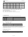
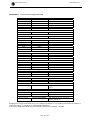
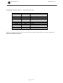
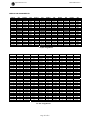
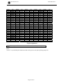
HYTEC ELECTRONICS Ltd
5 CRADOCK ROAD, READING, BERKS. RG2 0JT, UK
Telephone: +44 (0) 118 9757770
Fax: +44 (0)118 9757566
E-mail: [email protected]
Copyright 2008, Hytec Electronics Ltd
Data and specifications are subject to change without notice
VCB8004 VME 64x
INDUSTRY PACK
CARRIER BOARD
USERS MANUAL
PCB Issue 1.0
Xilinx Version 8004V101
Document Nos.: 8004/UTM/G/x/1.0
Date: 29/02/2008
Author: MRN
Hytec Electronics Ltd
8004/UTM/G/2/1.0
CONTENTS
1.
PRODUCT DESCRIPTION......................................................................................................................................3
1.1
2.
KEY FEATURES .....................................................................................................................................................4
USE OF THE VME DATA BUS AND MEMORY ACCESS.................................................................................5
2.1
VME ADDRESSING ...............................................................................................................................................5
2.1.1 Short Addressing (A16 AM29h and 2Dh)........................................................................................................5
2.1.2 Standard Addressing (A24 AM39h and 3Dh)..................................................................................................6
2.1.3 Carrier board Configuration ROM (A24 AM2Fh).........................................................................................6
2.2
MEMORY ACCESS .................................................................................................................................................6
2.2.1 IP Memory Size................................................................................................................................................6
2.2.2 Carrier Board IP Memory Map ......................................................................................................................7
2.2.3 Extended Addressing (A32 AM08, AM0C AM09, AM0D, AM0B and AM0F) ................................................7
3.
ON BOARD FEATURES ..........................................................................................................................................7
3.1
IP STATUS REGISTER (READ ONLY).....................................................................................................................7
3.2
MEMORY OFFSET (READ/WRITE) ........................................................................................................................7
3.3
CONTROL & STATUS REGISTER CARRIER BOARD (CSR CB)................................................................................8
3.4
IP INTERRUPT SELECT REGISTER (READ/WRITE).................................................................................................8
3.5
VME SYSTEM AND BOARD RESETS ......................................................................................................................9
3.5.1 A VME system reset will clear the following registers:...................................................................................9
3.5.2 A board reset generated from the CSR CB bit 0 will clear the following registers: .......................................9
4.
INTERRUPT SETTINGS..........................................................................................................................................9
5.
MEMORY 32BIT OR 64BIT DATA TRANSFERS .............................................................................................10
6.
VME64X KEYING AND ALIGNMENT PINS .....................................................................................................10
APPENDIX A
PCB JUMPERS....................................................................................................................................11
APPENDIX B
CARRIER BOARD CONFIGURATION ROM ................................................................................12
APPENDIX C ID PROM REGISTERS (GREENSPRING FORMAT) .....................................................................13
PRODUCT SPECIFICATIONS ......................................................................................................................................14
VME64X PIN ASSIGNMENTS.......................................................................................................................................15
Page 2 of 16
Hytec Electronics Ltd
8004/UTM/G/3/1.0
1. PRODUCT DESCRIPTION
The VCB 8004 is a 6U (double height) VME board constructed to the VME64x standard, with EMC front
panel, injector/ejector handles, guide pin and slot keying, static discharge protection, hot swap capability, blue
power up LED, geographical or jumper selected addressing, 5-row P1 and P2 connectors and 5-row P0
connector.
The module features hot-swap capability with auto power up and host interaction. An on-board FPGA allows
full mapping of the IP board memory, I/O and ID spaces.
The VME interface supports short I/O access A16: D16:D08 (EO), standard I/O access A24:D16:D08 (EO)
and extended memory access A32: D64: D32: D16.
The module also has the ability to carry out MBLT A32 D64 and BLT A32:D32:D16 data transfers on IP
memory space.
Four Industry Pack sites are available and can accept 4 single-size Industry Packs. The board has the
capability to multiple-address the memory of IP sites and read/write data to them simultaneously using a data
width of 32 or 64 bits.
The carrier board supports 8MHz and 32MHz IP interfaces.
One of VMEbus interrupt lines IRQ1 to IRQ7 can be selected and enabled by writing to an on-board register.
The Industry Pack interrupt lines IntReq0* and IntReq1* from each of the four sites can be enabled on an
individual basis and mapped to the selected VME IRQ line.
Four front panel mounted LED’s flash to visually confirm completed IP access cycles to individual slots.
There is a TTL ‘Inhibit’ input on the front panel that allows connection to any or all of the IP card Strobe*
lines through jumpers. The signal is routed through this pin on the IP logic connector to allow overall control
to be applied to IP boards in data acquisition systems.
The ‘GO’ output can be connected to the ‘Inhibit’ input through a jumper to synchronise timing between
carrier boards.
The carrier board has some thickened I/O tracks to allow the IP boards to be powered externally to give full
isolation.
All I/O is via the VME backplane P0 and P2 connectors as specified in the VME64 extensions specification.
The signals connect to the industry pack sites according to the VME64x Greenspring pinout for IP module
carriers.
Hytec has a number of rear-mounted transition cards with high-density 50-way [SCSI2] connectors, which can
cater for all 200 IP I/O signals and provide any necessary signal conditioning.
Page 3 of 16
Hytec Electronics Ltd
8004/UTM/G/4/1.0
1.1 Key Features
•
VME64 extensions / Industry Pack Carrier Board
•
VME64x rear panel I/O
•
Base Address decoding by either Geographical addressing or jumper selectable
•
IP memory space accesses software configurable from 1Mbyte to 8Mbytes
•
MBLT D64 operation for simultaneous memory data access to all four IP sites
•
BLT or Single D32 operation for simultaneous memory data access to two IP sites
•
BLT or Single D16 operation for memory data access to one IP site
•
IP module Clock speeds can be individually selected to be 8MHz or 32MHz by software.
•
Full EMC shielding and insertion/extraction handles
•
Fully Hot-Swap capable with auto power-up and host interaction
•
6U (double height) VME base card
•
User selectable VME interrupt level via software programmable registers
•
Up to two interrupt requests are supported for each IP module
•
Interrupt release mechanism RORA or ROAK software selectable
•
Front panel TTL Go/Inhibit signals allow control of IP timing synchronisation
•
Thickened I/O lines to allow externally power supply to IPs
•
VME 64x Configuration ROM
•
On-board 32MHz clock generation
•
VME64x guide pin and slot keying
•
3.3V and 5V supply to P2 connector
•
Self-resetting PTC fuses on all the IP power supplies
Page 4 of 16
Hytec Electronics Ltd
8004/UTM/G/5/1.0
2. USE OF THE VME DATA BUS AND MEMORY ACCESS
2.1 VME Addressing
The module uses A16/D16/D08 (EO) (Even and Odd byte3) or A24/D16/D08 (EO) for accesses to the IP I/O,
IP ID and Carrier board Configuration Registers.
The base address of these areas are set either by PCB jumpers (J6 to J10) or by VME64x geographical
addressing lines GA0 to GA4.
Address
I/O Base+
Offset
0x0000
I/O Base+
0x0080
I/O Base+
0x0100
I/O Base+
0x0180
I/O Base+
0x0200
I/O Base+
0x0280
I/O Base+
0x0300
I/O Base+
0x0380
I/O Base+
0x0400
I/O Base +
0x0420
I/O Base +
0x0440
I/O Base+
0x0480
I/O Base+
0x0600
Range
Assignment
0x0000
IP A I/O Space
0x007E
0x0080
IP A ID Space
0x00FE
0x0100
IP B I/O Space
0x017E
0x0180
IP B ID Space
0x01FE
0x0200
IP C I/O Space
0x027E
0x0280
IP C ID Space
0x02FE
0x0300
IP D I/O Space
0x037E
0x0380
IP D ID Space
0x03FE
0x0400
Carrier on board registers
0x041E
0x0420
SHARC Control Registers
0x043E
(option)
0x0440
Dual-Ported SRAM accessible
0x047E
from VME and SHARC (option)
0x0480
Green Springs Type ID
0x04FF
0x0600
VME64x configuration ROM
0x07FF
(See appendix B)
8004 A16 and A24 address Map
Size
128 Bytes
128 Bytes
128 Bytes
128 Bytes
128 Bytes
128 Bytes
128 Bytes
128 Bytes
32 Bytes
32 Bytes
64 Bytes
128 Bytes
512 Bytes
2.1.1 Short Addressing (A16 AM29h and 2Dh)
In Short address mode the geographical addressing lines equate to the address lines GA0 =A11 to GA4=A15
and the jumper address setting J6=A11 to J10=A15.
A11 - A15 is the module address determined by the setting of the relevant PCB jumpers or geographical
address lines
IP I/O, IP ID and Carrier board Configuration Registers:
AM29 Short (A16) non-privileged.
AM2D Short (A16) supervisory.
Page 5 of 16
Hytec Electronics Ltd
8004/UTM/G/6/1.0
2.1.2 Standard Addressing (A24 AM39h and 3Dh)
The A24 base address is determined either by PCB jumper settings J6=A19 to J10=A23 or by geographical
addressing lines GA0 =A19 to GA4=A23.
IP I/O, IP ID and Carrier board Configuration Registers:
AM39 Standard (A24) non-privileged.
AM3D Standard (A24) supervisory.
2.1.3 Carrier board Configuration ROM (A24 AM2Fh)
See appendix B for the contents of the configuration ROM.
AM2F Configuration ROM/Control & Status Registers. Address selection as above
2.2 Memory Access
The module uses A32/D64/D32/D16 for accesses to the IP memory.
The base address of the memory can be set by either the Geographical address lines/Manual jumpers or by
using the Memory Offset Register. Writing a ‘1’ to bit ‘6’ of the CSR CB (base+8h) selects the Memory
Offset Register to set the base address.
Using the Memory Offset Register to store the base address allows the address lines A22 to A31 to be used to
set the base address.
Geographical addressing uses the lines GA0=A22 to GA4=A26.
First need to select whether Geographical address lines or the Memory Offset register are to define the
extended memory start address. This is selected using MEM MODE (bit 6) of the CSR CB register.
MEM MODE (bit 6 CSR )
0
1
Memory Addressing Mode
Geographical address lines
Memory Offset register
Bit 6 CSR CB setting the memory address mode
2.2.1 IP Memory Size
Some controllers have a limited memory range so to take account of this when using geographical and register
addressing the memory size allocated to each IP card can be controlled:CSR CB
IPMS1
IPMS0
(bit 8)
(bit 7)
0
0
0
1
1
0
1
1
IP Memory Size
1MB
2MB
4MB
8MB
Address Lines
Geographical
Memory Offset
Addressing
Reg
A22-A26
A22-A31
A23-A26
A23-A31
N/A
A24-A31
A27-A31
A25-A31
Here the GA address is shifted up one. This only allows 16 slots to be used
with geographical Addressing
2.2.2 Carrier Board IP Memory Map
Address
Memory Range
Page 6 of 16
Memory
Hytec Electronics Ltd
Memory Base +
Memory Base +
Memory Base +
Memory Base +
8004/UTM/G/7/1.0
1MB
0x000000
0x0FFFFF
0x100000
0x1FFFFF
0x200000
0x2FFFFF
0x300000
0x3FFFFF
2MB
0x000000
0x1FFFFF
0x200000
0x3FFFFF
0x400000
0x5FFFFF
0x600000
0x6FFFFF
4MB
0x000000
0x3FFFFF
0x400000
0x7FFFFF
0x800000
0xBFFFFF
0xC00000
0xFFFFFF
8MB
0x000000
0x7FFFFF
0x800000
0xFFFFFF
0x1000000
0x17FFFFF
0x1800000
0x1FFFFFF
Assignment
IP A
IP B
IP C
IP D
2.2.3 Extended Addressing (A32 AM08, AM0C AM09, AM0D, AM0B and AM0F)
A32 Memory Address Modifiers:
Single - AM09 or AM0D (extended non-priv. or supervisory)
BLT - AM0B or AM0F (extended non-priv. or supervisory)
MBLT - AM08 or AM0C (extended non-priv. or supervisory) 64 bit block transfer.
3. ON BOARD FEATURES
The configuration and control of the 8004 module is achieved by the following registers:
Base
Base +
Base +
Base +
Base +
Base +
Offset
0x400
0x404
0x408
0x40C
0x410
3.1
Register
Description
IP Status
Allows state of IP INT and Error flags to be monitored
Memory Offset
Sets base address of IP memory areas
Control & Status Register CB Set up of 8004 carrier card
IP Interrupt Select
Selects IP interrupts to be mapped to VME IRQ
Not Use
None
8004 On-Board Registers
IP Status Register (Read Only)
Address:
Read = Base + 0x0400
D15
D14
D13
D12
DMA DMA DMA DMA
REQ REQ REQ REQ
D0
C0
B0
A0
D11
NU
D10
NU
D09
NU
D08
IP
ERR
D07
INT
REQ
D1
D06
INT
REQ
C1
D05
INT
REQ
B1
D04
INT
REQ
A1
D03
INT
REQ
D0
D02
INT
REQ
C0
D01
INT
REQ
B0
D00
INT
REQ
A0
Two interrupt status, one DMA status (not used) and one error status bits for each of IP sites A – D.
IP ERR Open drain signal can be driven by any IP card. The Industrial I/O Pack specification states that the
error signals indicate a non-recoverable error from the IP module. See your IP documentation for a
description of the error signal if used.
3.2 Memory Offset (Read/Write)
Address: Base + 0x0404
D15
A31
D14
A30
D13
A29
D12
A28
D11
A27
D10
A26
D09
A25
D08
A24
D07
A23
D06
A22
D05
x
D04
x
D03
x
D02
x
D01
x
D00
x
‘x’ = don’t care
This register defines the IP memory base address when selected by MEMMODE=’1’ in CSR CB.
Page 7 of 16
Hytec Electronics Ltd
8004/UTM/G/8/1.0
3.3 Control & Status Register Carrier Board (CSR CB)
Control (Write)
Address: Base + 0x0408
D15
D14
AB
32Bit
CD
32Bit
D13
IP D
CLK
D12
IP C
CLK
D11
IP B
CLK
D10 D09 D08 D07 D06 D05
D04
D03
D02
D01 D00
IP A INT IPMS IPMS MEM IPCLK INTSEL INTSEL INTSEL
INTEN Rst
CLK RELS
1
0 MODE SEL
2
1
0
Status
(Read)
Address: Base + 0x0408
D15
D14
AB
32Bit
CD
32Bit
D13
IP D
CLK
D12
IP C
CLK
D11
IP B
CLK
D10 D09 D08 D07 D06
D05
D04
D03
D02
D01
D00
IP A INT IPMS IPMS MEM IPCLK INTSEL INTSEL INTSEL INTEN Rst
CLK RELS 1
0 MODE SEL
2
1
0
Rst
INTEN
INTSEL0
INTSEL1
INTSEL2
IPCLKSEL
MEMMODE
IP MS0
IP MS1
INT RELS
IP A CLK
IP B CLK
IP C CLK
IP D CLK
CD32bit
AB32bit
Clears status register to zero when written as a ‘1’.
Enable interrupt from carrier board to VMEbus backplane.
Select VME interrupt level.
Select VME interrupt level. (See section 4).
Select VME interrupt level.
0= Sel 8MHz IP clock or as set by IP A to D CLK 1=32MHz clock on all sites
Select memory base address to be defined by geographical address lines=0 or by Memory
offset vector register=1.
Set IP memory size.
Set IP memory size. (See section 2.2)
Interrupt release RORA=0 and ROAK = 1 (see section 4)
Set IP A clock speed 0 = 8MHz and 1 = 32MHz (If IPCLKSEL=1 overrides this setting).
Set IP B clock speed 0 = 8MHz and 1 = 32MHz (If IPCLKSEL=1 overrides this setting).
Set IP C clock speed 0 = 8MHz and 1 = 32MHz (If IPCLKSEL=1 overrides this setting).
Set IP D clock speed 0 = 8MHz and 1 = 32MHz (If IPCLKSEL=1 overrides this setting).
Enables 32-bit data access to IP sites C&D
Enables 32-bit data access to IP sites A&B
3.4 IP Interrupt Select Register (Read/Write)
Address: Base + 0x040C
D15
NU
D14
NU
D13
NU
D12
NU
D11
NU
D10
NU
D09
NU
D08
NU
D07
D06
D05
D04
D03
D02
D01
D00
IPINT IPINT IPINT IPINT IPINT IPINT IPINT IPINT
D1
C1
B1
A1
D0
C0
B0
A0
This selects which IP interrupt request lines will be enabled.
‘1’ = corresponding IP card interrupt enabled.
Page 8 of 16
Hytec Electronics Ltd
8004/UTM/G/9/1.0
3.5 VME System and Board Resets
3.5.1 A VME system reset will clear the following registers:
•
•
•
CSR CB
Memory Offset Register
IP Interrupt Select register
3.5.2 A board reset generated from the CSR CB bit 0 will clear the following registers:
•
•
CSR CB
IP Interrupt Select register
4. INTERRUPT SETTINGS
The interrupt level generated by the carrier board is set using the CSR CB register INTSEL0 (bit 2), INTSEL1
(bit 3), and INTSEL2 (bit 4).
Interrupt Level
None
IRQ 1
IRQ 2
IRQ 3
IRQ 4
IRQ 5
IRQ 6
IRQ 7
INTSEL 2 INTSEL 1 INTSEL 0
0
0
0
0
0
1
0
1
0
0
1
1
1
0
0
1
0
1
1
1
0
1
1
1
VME Interrupt Level Select
The IP Interrupt Select register allows the user to enable only the IP interrupts required and mask off the rest.
To select an IP interrupt write a ‘1’ to the appropriate bit of the register see section 3.4 above.
The interrupt vector is held on the individual IP cards.
To enable VME interrupts from the carrier board to the VMEbus backplane set bit 1 of the CSR CB to ‘1’.
Writing a ‘0’ to this register disables the interrupts.
The VME interrupt is released by clearing the interrupt enable bit INTEN (bit 1) in the CSR on acknowledge.
If bit 9 set to ‘1’ in CSR The VME interrupt is cleared when it is acknowledged [ROAK protocol].
If bit 9 set to ‘0’ in the CSR the interrupt is released when the interrupt service routine clears the interrupt
enable bit [RORA protocol]. in the CSR (bit 1 INTEN) .
The IP interrupts are prioritised in the 8004 where IP A has the highest and IP D the lowest.
Each IP card can be loaded with a separate IP vector and when an interrupt occurs the controller will be given
the interrupt vector of the highest priority IP card currently asserting either of its interrupt lines.
If all four card interrupt at the same time then IP A will be serviced first then IP B then IP C and finally IP D.
Reading the IP Status register of the 8004 at base + 0x0400 (READ ONLY) shows which IP cards have
interrupts pending.
Page 9 of 16
Hytec Electronics Ltd
8004/UTM/G/10/1.0
5. MEMORY 32BIT OR 64BIT DATA TRANSFERS
To carry out a 32bit data transfer set the relevant AB32(bits 15) or CD32(bits 14) bits in the CSR and address
the first IP module of the pair i.e. ‘A’ for AB32 and ‘C’ for CD32.
There is no need to set AB32 or CD32 for a MBLT data transfer as these are ignored as it is 64 bit only.
When doing an MBLT must address IP site ‘A’.
When doing a 32bit or 64bit data transfer the clocks for the IP modules involved must be the same either
8MHz or 32MHz as set in the CSR bits 10 to 13.
6. VME64x KEYING AND ALIGNMENT PINS
The keying mechanism provides for three key holes on top and three keying holes on the bottom of each board
and subrack slot. Each key hole can be keyed with a “No Key” or a keying peg in one of four positions. With
three key holes top and bottom the scheme provides a total of 15,625 keying combinations.
Page 10 of 16
Hytec Electronics Ltd
APPENDIX A
8004/UTM/G/11/1.0
PCB JUMPERS
Hytec 8004 IP Carrier Board
J1
J2
J3
J4
J5
J6 – J10
J11
J12
J17
Connects the common strobe line from the FPGA to Industry Pack C Logic Connector pin 46.
Must be IN Factory set.
Connects the common strobe line from the FPGA to Industry Pack A Logic Connector pin 46.
Supplies switched and fused +5V to pins P2 A32 and P2 C32 (Delivered Not selected).
Connects the common strobe line from the FPGA to Industry Pack B Logic Connector pin 46.
Base address:. Make according to required A11-A15 base address short IO addressing or A19 – A23
for A24 Standard addressing
Connects the common strobe line from the FPGA to Industry Pack D Logic Connector pin 46.
This is Factory set.
Selects GO to be driven by either INHIBIT front panel lemo or from FPGA logic in this version of
the firmware the FPGA drives GO high. In this version the jumper should be either removed or in
the INH position.
Note: The reference to the ‘Common Strobe Line’ refers to the front panel Inhibit signal which is passed
through by the FPGA unprocessed, thus asserting the Inhibit input low will drive all connected IP logic
connector pins 46 (Strobe*) low.
J13, J14, ,J15 and J16 Not used in this version.
Set Base Address Jumpers J6 – J10
To use VME64 geographical addressing lines all jumpers should be inserted in to position AUTO.
To use the user set base address removing all Base address jumpers from positions AUTO and insert the
required jumpers in to positions MANUAL.
With no jumpers in position MANUAL for J6 to J10 the address is 0x0000 A16 or 0x000000 A24.
With one jumpers in position MANUAL for J6 the address is 0x0800 A16 or 0x080000 A24.
With all jumpers in position MANUAL for J6 to J10 the address is 0xF800 A16 or 0xF80000 A24.
Base Addrs
(Hex)
A16
0000
0800
1000
1800
:
:
E000
E800
F000
F800
A24
000000
080000
100000
180000
:
:
E00000
E80000
F00000
F80000
A15
(Manual)
A14
(Manual)
A13
(Manual)
A12
(Manual)
A11
(Manual)
OUT
OUT
OUT
OUT
:
:
IN
IN
IN
IN
OUT
OUT
OUT
OUT
:
:
IN
IN
IN
IN
OUT
OUT
OUT
OUT
:
:
IN
IN
IN
IN
OUT
OUT
IN
IN
:
:
OUT
OUT
IN
IN
OUT
IN
OUT
IN
:
:
OUT
IN
OUT
IN
Page 11 of 16
Hytec Electronics Ltd
APPENDIX B
8004/UTM/G/12/1.0
Carrier Board Configuration ROM
Address Offset
0x03
0x07
0x0B
0x0F
0x13
0x17
0x1B
0x1F
0x23
0x27
0x2B
0x2F
Value
C1
00
02
00
Definition
Check Sum
Length of ID ROM MSB
Length of ID ROM
Length of ID ROM LSB
Configuration ROM data access width
0x83
CSR data access width
0x83
CSR space Specification ID
VME64x-1997
0x02
Identify a Valid CR
‘C’
0x43
‘R’
0x52
Manufacturer’s ID
0x00
0x80
0x03
Board ID
0x33
0x37
0x3B
0x3F
0x80
0x04
0x00
0x00
Revision ID
0x43
0x47
0x4B
0x4F
0x01
0x05
0x00
0x01
PCB issue
Xilinx version
Xilinx revision nos
Xilinx revision nos
ASCII string null terminated or 0x000000
0x53
0x57
0x5B
0x00
0x00
0x00
Program ID code
0x7F
0x01
No program, ID ROM only
Interrupt Capabilities
0xF7
0xFE
Denotes support for Int levels 7 – 1.
Data Access Width
0x103
0x84
Accepts D32, D16 or D08(EO)
cycles
Board Serial Number
0xCB, 0xCF, 0xD3
0xD7, 0xDB, 0xDF
0x
0x
BEG_SN MSB
END_SN LSB
0x123.. 0x13F
0x2200A2000000BB00
AM code mask
AM codes 3D, 39, 2F, 2D, 29, 0F,
0D, 0C, 0B, 09, 08
Reading the Configuration ROM using A16 (AM29 and AM2D) or A24 (AM39 and AM3D) the address is
VME base address + 0x0600, the Configuration ROM offset.
Can read Configuration ROM using A24 AM2F starting at base address + 0x0000.
Page 12 of 16
Hytec Electronics Ltd
8004/UTM/G/13/1.0
APPENDIX C ID PROM Registers (GreenSpring Format)
Address Offset
0x481
0x483
0x485
0x487
0x489
0x48B
0x48D
0x48F
0x491
0x493
0x495
0x487
Value
0x49
0x50
0x41
0x43
0x80
0x84
0x0x
0x00
0x00
0x00
0x0C
Definition
ASCII “I”
ASCII “P”
ASCII “A”
ASCII “H”
Manufacturer’s ID
Model Number
Revision
Reserved
Driver ID, low byte
Driver ID, high byte
No of bytes used
CRC
The low four bytes contain the ASCII text “IPAH” this signifies that the 8004 carrier board supports the
8MHz and 32MHz IP interfaces.
Page 13 of 16
Hytec Electronics Ltd
8004/UTM/G/14/1.0
PRODUCT SPECIFICATIONS
Power Requirements
+5V @ 600mA typical
+12V @ 30mA
-12V @ 30mA
+3.3V @ approx 10mA
Additional power maybe consumed by Industry Packs.
Operating Temperature Range
0 to +45 deg Celsius ambient.
Mechanical
6U single width VME module with access to 5 row P0, P1 and P2 connectors.
IP Memory Mapping
VME Access Single A32:D32, D16, D8 (EO) AM Codes: 09h and 0Dh.
VME Access BLT A32:D32, D16, D8 (EO) AM Codes: 0Bh and 0Fh.
VME Access MBLT A32:D64
AM Codes: 08h and 0Ch
IP I/O Mapping
VME Access A16:D16:D8 (EO) AM Codes: 29h and 2Dh.
VME Access A24:D16:D8 (EO) AM Codes: 39h and 3Dh.
Front Panel Indicators and Inputs
‘VME’
LED (green)
‘Not Configured
LED (blue)
IP ACK
4 LED’s (red)
Illuminates for a minimum of 20msecs whenever the
module is accessed via the VME bus.
Indicates the state of the VME module during hot swap
operation.
Indicate when an IP card has sent an ACK.
Front Panel Connectors
Input to supply common IP sites
Inhibit
Single TTL input. This input has a 10K pull-up resistor to 3.3Volt supply.
Connector type: LEMO ‘00’
Go
Single output. This output may be connected by a jumper to the Inhibit input signal for
propagation of Inhibit from carrier to carrier.
Connector type: LEMO ‘00’
Page 14 of 16
Hytec Electronics Ltd
8004/UTM/G/15/1.0
VME64x PIN ASSIGNMENTS
ROW A
P0.A01
P0.A02
P0.A03
P0.A04
P0.A05
P0.A06
P0.A07
P0.A08
P0.A09
P0.A10
P0.A11
P0.A12
P0.A13
P0.A14
P0.A15
P0.A16
P0.A17
P0.A18
P0.A19
SIG
IODO1
IOD06
IOD11
IOD16
IOD21
IOD26
IOD31
IOD36
IOD41
IOD46
IOC01
IOC06
IOC11
IOC16
IOC21
IOC26
IOC31
IOC36
IOC41
ROW B
P0.B01
P0.B02
P0.B03
P0.B04
P0.B05
P0.B06
P0.B07
P0.B08
P0.B09
P0.B10
P0 B11
P0.B12
P0.B13
P0.B14
P0.B15
P0.B16
P0.B17
P0.B18
P0.B19
SIG
IOD02
IOD07
IOD12
IOD17
IOD22
IOD27
IOD32
IOD37
IOD42
IOD47
IO002
IO007
IO012
IO017
IOC22
IO027
IO032
IO037
IO042
ROW C
P0.C01
P0.C02
P0.C03
P0.C04
P0.C05
P0.C06
P0.C07
P0.C08
P0.C09
P0.C10
P0.C11
P0.C12
P0.C13
P0.C14
P0.C15
P0.C16
P0.C17
P0.C18
P0.C19
SIG
IOD03
IOD08
IOD13
IOD18
IOD23
IOD28
IOD33
IOD38
IOD43
IOD48
IOC03
IOC08
IOC13
IOC18
IOC23
IOC28
IOC33
IOC38
IOC43
ROW D
P0.DO1
P0.D02
P0.D03
P0.D04
P0.D05
P0.D06
P0.D07
P0.D08
P0.D09
P0.D10
P0.D11
P0.D12
P0.D13
P0.D14
P0.D15
P0.D16
P0.D17
P0.D18
P0.D19
SIG
IOD04
IOD09
IOD14
IOD19
IOD24
IOD29
IOD34
IOD39
IOD44
IOD49
IOC04
IOC09
IOC14
IOC19
IOC24
IOC29
IOC34
IOC39
IOC44
ROW E
P0.E01
P0.E02
P0.E03
P0.E04
P0.E05
P0.E06
P0.E07
P0.E08
P0.E09
P0.E10
P0 E11
P0.E12
P0.E13
P0.E14
P0.E15
P0.E16
P0.E17
P0.E18
P0.E19
SIG
IOD05
IODlO
IOD15
IOD20
IOD25
IOD30
IOD35
IOD40
IOD45
IOD50
IOC05
IOC10
IOC15
IOC20
IOC25
IOC30
IOC35
IOC40
IOC45
ROW F
P0.F01
P0.F02
P0.F03
P0.F04
P0.F05
P0.F06
P0.F07
P0.F08
P0.F09
P0.F10
P0.F11
P0.F12
P0.F13
P0.F14
P0.F15
P0.F16
P0.F17
P0.F18
P0.F19
SIG
GND
GND
GND
GND
GND
GND
GND
GND
GND
GND
GND
GND
GND
GND
GND
GND
GND
GND
GND
P0 pin assignments
P1 ROW A
P1.A01
P1.A02
P1.A03
P1.A04
P1.A05
P1.A06
P1.A07
P1.A08
P1.A09
P1.A10
P1.A11
P1.A12
P1.A13
P1.A14
P1.A15
P1.A16
P1.A17
P1.A18
P1.A19
P1.A20
P1.A21
P1.A22
P1.A23
P1.A24
P1.A25
P1.A26
P1.A27
P1.A28
P1.A29
P1.A30
P1.A31
P1.A32
SIGNAL
D00
D01
D02
D03
D04
D05
D06
D07
GND
N/C
GND
DS1*
DS0*
WRITE
GND
DTACK*
GND
AS
GND
IACK
IACKIN*
IACKOUT
AM4
A07
A06
A05
A04
A03
A02
A0l
-12V
+5V
P1 ROW B
P1.B01
P1.B02
P1.B03
P1.B04
P1.B05
P1.B06
P1.B07
P1.B08
P1.B09
P1.B10
P1.B11
P1.B12
P1.B13
P1.B14
P1.B15
P1.B16
P1.B17
P1.B18
P1.B19
P1.B20
P1.B21
P1.B22
P1.B23
P1.B24
P1.B25
P1.B26
P1.B27
P1.B28
P1.B29
P1.B30
P1.B31
P1.B32
SIGNAL
N/C
N/C
N/C
BG0IN*
BG0OUT*
BG1IN*
BG1OUT*
BG2IN*
BG2OUT*
BG3IN*
BG3OUT*
N/C
N/C
N/C
N/C
AM0
AM1
AM2
AM3
GND
N/C
N/C
GND
IRQ7*
IRQ6*
IRQ5*
IRQ4*
IRQ3*
IRQ2*
IRQ1*
N/C
+5V
P1 ROW C
P1.C01
P1.C02
P1.C03
P1.C04
P1.C05
P1.C06
P1.C07
P1.C08
P1.C09
P1.C10
P1.C11
P1.C12
P1.C13
P1.C14
P1.C15
P1.C16
P1.C17
P1.C18
P1.C19
P1.C20
P1.C21
P1.C22
P1.C23
P1.C24
P1.C25
P1.C26
P1.C27
P1.C28
P1.C29
P1.C30
P1.C31
P1.C32
SIGNAL
D08
D09
D10
D11
D12
D13
D14
D15
GND
N/C
BERR*
RESET
LWORD*
AM5
A23
A22
A21
A20
A19
A18
A17
A16
A15
A14
A13
A12
A11
A10
A09
A08
+12V
+5V
P1 Pin Assignments
Page 15 of 16
P1 ROW D
P1.D01
P1.D02
P1.D03
P1.D04
P1.D05
P1.D06
P1.D07
P1.D08
P1.D09
P1.D10
P1.D11
P1.D12
P1.D13
P1.D14
P1.D15
P1.D16
P1.D17
P1.D18
P1.D19
P1.D20
P1.D21
P1.D22
P1.D23
P1.D24
P1.D25
P1.D26
P1.D27
P1.D28
P1.D29
P1.D30
P1.D31
P1.D32
SIGNAL
N/C
N/C
N/C
N/C
N/C
N/C
N/C
N/C
N/C
N/C
N/C
+3.3V
N/C
+3.3V
N/C
+3.3V
N/C
+3.3V
N/C
+3.3V
N/C
+3.3V
N/C
+3.3V
N/C
+3.3V
N/C
+3.3V
N/C
+3.3V
N/C
+5V
P1 ROW Z
P1.Z01
P1.Z02
P1.Z03
P1.Z04
P1.Z05
P1.Z06
P1.Z07
P1.Z08
P1.Z09
P1.Z10
P1.Z11
P1.Z12
P1.Z13
P1.Z14
P1.Z15
P1.Z16
P1.Z17
P1.Z18
P1.Z19
P1.Z20
P1.Z21
P1.Z22
P1.Z23
P1.Z24
P1.Z25
P1.Z26
P1.Z27
P1.Z28
P1.Z29
P1.Z30
P1.Z31
P1.Z32
SIGNAL
N/C
GND
N/C
GND
N/C
GND
N/C
GND
N/C
GND
N/C
GND
N/C
GND
N/C
GND
N/C
GND
N/C
GND
N/C
GND
N/C
GND
N/C
GND
N/C
GND
N/C
GND
N/C
GND
Hytec Electronics Ltd
ROWA
P2.A01
P2.A02
P2.A03
P2.A04
P2.A05
P2.A06
P2.A07
P2.A08
P2.A09
P2.A10
P2.A11
P2.A12
P2.A13
P2.A14
P2.A15
P2.A16
P2.A17
P2.A18
P2.A19
P2.A20
P2.A21
P2.A22
P2.A23
P2.A24
P2.A25
P2.A26
P2.A27
P2.A28
P2.A29
P2.A30
P2.A31
P2.A32
SIG
IOB41
IOB43
IOB45
IOB47
IOB49
IOA01
IOA03
IOA05
IOA07
IOA09
IOA11
IOA13
IOA15
IOA17
IOA19
IOA21
IOA23
IOA25
IOA27
IOA29
IOA31
IOA33
IOA35
IOA37
IOA39
IOA41
IOA43
IOA45
IOA47
IOA49
+3.3V
Out+5V
ROWB
P2.B01
P2.B02
P2.B03
P2.B04
P2.B05
P2.B06
P2.B07
P2.B08
P2.B09
P2.B10
P2.B11
P2.B12
P2.B13
P2.B14
P2.B15
P2.B16
P2.B17
P2.B18
P2.B19
P2.B20
P2.B21
P2.B22
P2.B23
P2.B24
P2.B25
P2.B26
P2.B27
P2.B28
P2.B29
P2.B30
P2.B31
P2.B32
8004/UTM/G/16/1.0
SIG
+5V
GND
N/C
A24
A25
A26
A27
A28
A29
A30
A31
GND
+5V
N/C
N/C
N/C
N/C
N/C
N/C
N/C
N/C
GND
N/C
N/C
N/C
N/C
N/C
N/C
N/C
N/C
GND
+5V
ROWC
P2.C01
P2.C02
P2.C03
P2.C04
P2.C05
P2.C06
P2.C07
P2.C08
P2.C09
P2.C10
P2.C11
P2.C12
P2.C13
P2.C14
P2.C15
P2.C16
P2.C17
P2.C18
P2.C19
P2.C20
P2.C21
P2.C22
P2.C23
P2.C24
P2.C25
P2.C26
P2.C27
P2.C28
P2.C29
P2.C30
P2.C31
P2.C32
SIG
IOB42
IOB44
IOB46
IOB48
IOB50
IOA02
IOA04
IOA06
IOA08
IOA10
IOA12
IOA14
IOA16
IOA18
IOA20
IOA22
IOA24
IOA26
IOA28
IOA30
IOA32
IOA34
IOA36
IOA38
IOA40
IOA42
IOA44
IOA46
IOA48
IOA50
+3.3V
Out+5V
ROWD
P2.D01
P2.D02
P2.D03
P2.D04
P2.D05
P2.D06
P2.D07
P2.D08
P2.D09
P2.D10
P2.D11
P2.D12
P2.D13
P2.D14
P2.D15
P2.D16
P2.D17
P2.D18
P2.D19
P2.D20
P2.D21
P2.D22
P2.D23
P2.D24
P2.D25
P2.D26
P2.D27
P2.D28
P2.D29
P2.D30
P2.D31
P2.D32
SIG
IOC47
IOC48
IOC50
IOB0l
IOB03
IOB04
IOB06
IOB07
IOB09
IOB10
IOB12
IOB13
IOB15
IOB16
IOB18
IOB19
IOB21
IOB22
IOB24
IOB25
IOB27
IOB28
IOB30
IOB31
IOB33
IOB34
IOB36
IOB37
IOB39
IOB40
N/C
+5V
ROWZ
P2.Z01
P2.Z02
P2.Z03
P2.Z04
P2.Z05
P2.Z06
P2.Z07
P2.Z08
P2.Z09
P2.Z10
P2.Z11
P2.Z12
P2.Z13
P2.Z14
P2.Z15
P2.Z16
P2.Z17
P2.Z18
P2.Z19
P2.Z20
P2.Z21
P2.Z22
P2.Z23
P2.Z24
P2.Z25
P2.Z26
P2.Z27
P2.Z28
P2.Z29
P2.Z30
P2.Z31
P2.Z32
SIG
IOC46
GND
IOC49
GND
IOB02
GND
IOB05
GND
IOB08
GND
IOB11
GND
IOB14
GND
IOB17
GND
IOB20
GND
IOB23
GND
IOB26
GND
IOB29
GND
IOB32
GND
IOB35
GND
IOB38
GND
+3.3V
GND
P2 pin assignments
Denotes pins with thickened tracks which can be used for power inputs
Note:
‘Out+5V’ is provided by the 8004 board and can be put on to the pins by fitting jumper J4.
Page 16 of 16