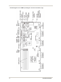
1
TRANSDUCTION
USER’S MANUAL
Version 1.0
05/31/12
TR-7053 INDUSTRIAL FULL-SIZE PICMG 1.3 SBC
WITH INTEL XEON E-1200 SERIES OR CORE i7 / i5 / i3 PROCESSOR
FOR INTEL PROCESSOR SOCKET LGA1155
23-5155 Spectrum Way, Mississauga, ON, Canada L4W 5A1
TEL: 1-800-268-0427, 905-625-1907
FAX: 905-625-0531
Email: [email protected]
Table of Contents
Chapter 1
Specifications .................................................................................................... 1
Introduction .............................................................................................................................. 1
Features .................................................................................................................................. 2
TR-7053 – Single Processor SHB Block Diagram .................................................................... 3
TR-7053 – Single Processor SHB Layout Diagram – Revision-01 (Top) .................................. 4
TR-7053 – Single Processor SHB Layout Diagram – Revision-02 (Top) .................................. 5
TR-7053 – Single Processor SHB Layout Diagram – Revision-03 and later (Top) ................... 6
TR-7053 – Single Processor SHB Layout Diagram (Bottom) ................................................... 7
Processor ................................................................................................................................ 8
Supported Intel® Processor Technologies ............................................................................... 8
Serial Interconnect Interface .................................................................................................... 9
Data Path ................................................................................................................................ 9
Serial Interconnect Speeds ...................................................................................................... 9
Platform Controller Hub (PCH) ................................................................................................ 9
Intel® Direct Media Interface (DMI) ......................................................................................... 9
Intel® Flexible Display Interface (FDI) Between CPU and PCH ............................................... 9
Memory Interface ..................................................................................................................... 9
DMA Channels ....................................................................................................................... 9
Interrupts ................................................................................................................................. 9
BIOS (Flash) ............................................................................................................................ 9
Cache Memory ........................................................................................................................ 9
DDR3-1333 Memory .............................................................................................................. 10
Universal Serial Bus (USB) .................................................................................................... 10
Analog Video Interface .......................................................................................................... 10
Digital Video Interface ............................................................................................................ 10
PCI Express Interfaces ......................................................................................................... 11
Ethernet Interfaces ............................................................................................................... 11
Serial ATA (SATA) Ports ....................................................................................................... 11
Watchdog Timer (WDT) .................................................................................................... 12-13
SATA RAID Operation (Windows O/S Setup) ........................................................................ 13
i
TR-7053 User Manual
Power Requirements ........................................................................................................ 13-14
Power Fail Detection ............................................................................................................. 14
Battery ................................................................................................................................... 14
Temperature/Environment ..................................................................................................... 14
Mechanical ............................................................................................................................ 14
Board Stiffener Bars ............................................................................................................. 15
Industry Certifications ........................................................................................................... 15
Configuration Jumpers ..................................................................................................... 16-17
P4A/P4B Ethernet LED’s and Connectors ............................................................................ 18
Status LED’s .................................................................................................................... 18-20
System BIOS Setup Utility .................................................................................................... 20
Connectors ...................................................................................................................... 21-27
Chapter 2
PCI Express® Reference .................................................................................. 29
Introduction ............................................................................................................................ 29
PCI Express Links ............................................................................................................ 29-30
SHB Configuration ................................................................................................................. 30
PCI Express Edge Connector Pin Assignments ................................................................ 31-33
PCI Express Signals Overview .............................................................................................. 34
Optional IOB33 PCI Express Link Expansion ........................................................................ 35
Chapter 3
TR-7053 System Power Connections ............................................................. 37
Introduction ............................................................................................................................ 37
Power Supply and SHB Interaction ................................................................................... 37-38
Electrical Connection Configurations ................................................................................ 38-39
Chapter 4
PCI Express Backplane Usuage ..................................................................... 41
Introduction ............................................................................................................................ 41
SHB Edge Connectors ...................................................................................................... 41-42
TR-7053 and Compatible Backplanes ................................................................................... 43
Chapter 5
Optional IOB33 Expansion Board Usage ....................................................... 45
IOB33 Overview .................................................................................................................... 45
IOB33 Features ..................................................................................................................... 45
ii
TR-7053 User Manual
IOB33 Temperature/Environment .......................................................................................... 45
IOB33 Block Diagram ............................................................................................................ 46
IOB33 Layout Diagram .......................................................................................................... 47
IOB33 I/O Plate Diagram ....................................................................................................... 47
IOB33 Connectors ............................................................................................................ 48-50
Chapter 6
BIOS .................................................................................................................. 52
Starting APTIO® TSE ........................................................................................................ 52-53
Advanced Setup ............................................................................................................... 55-58
Chipset Configuration Setup ............................................................................................. 59-60
Boot Setup ............................................................................................................................. 61
Security ................................................................................................................................. 63
Saving and Exiting BIOS Setup and Restoring Defaults ................................................... 65-66
Event Log .............................................................................................................................. 67
Appendix A BIOS Messages ................................................................................................ 69
Introduction ............................................................................................................................ 69
Aptio Boot Flow ..................................................................................................................... 69
BIOS Beep Codes ................................................................................................................. 69
PEI Beep Codes .................................................................................................................... 69
DXE Beep Codes .................................................................................................................. 70
BIOS Status Codes ............................................................................................................... 71
BIOS Status POST Code LED’s ............................................................................................ 71
Status Code Ranges ............................................................................................................. 72
SEC Status Codes ................................................................................................................. 72
SEC Beep Codes .................................................................................................................. 72
PEI Status Codes ............................................................................................................. 73-74
DXE Status Codes ............................................................................................................ 75-77
DXE Beep Codes .................................................................................................................. 77
ACPI/ASL Status Codes ........................................................................................................ 78
OEM – Reserved Status Code Ranges ................................................................................. 78
iii
TR-7053 User Manual
HANDLING PRECAUTIONS
WARNING: This product has components that may be damaged by electrostatic discharge.
To protect your system host board (SHB) from electrostatic damage, be sure to observe the following
precautions when handling or storing the board:
Keep the SHB in its static-shielded bag until you are ready to perform your installation.
Handle the SHB by its edges.
Do not touch the I/O connector pins.
Do not apply pressure or attach labels to the SHB.
Use a grounded wrist strap at your workstation or ground yourself frequently by touching the
metal chassis of the system before handling any components. The system must be plugged into an
outlet that is connected to an earth ground.
Use antistatic padding on all work surfaces.
Avoid static-inducing carpeted areas.
RECOMMENDED BOARD HANDLING PRECAUTIONS
This SHB has components on both sides of the PCB. Some of these components are extremely small and
subject to damage if the board is not handled properly. It is important for you to observe the following
precautions when handling or storing the board to prevent components from being damaged or broken off:
Handle the board only by its edges.
Store the board in padded shipping material or in an anti-static board rack.
Do not place an unprotected board on a flat surface.
iv
TR-7053 User Manual
Before You Begin
INTRODUCTION
It is important to be aware of the system considerations listed below before installing your TR-7053
(7053-xxx) SHB. Overall system performance may be affected by incorrect usage of these features.
DDR3-1333 MEMORY
Transduction recommends unbuffered ECC PC3-8500 or PC3-10600 DDR3 memory modules for use on the
TR-7053. These unbuffered ECC registered (64-bit) DDR3 DIMMs must be PC3-10600 or PC3-8500
compliant. Unbuffered non-ECC DDR3 DIMMs are also supported on the TR-7053 SHB, but you cannot
mix the two different memory types on the same board.
NOTES:
•
•
•
•
To maximize memory interface speed, populate each memory channel with DDR3
DIMMs having the same interface speed. The SHB will support DIMMs with different
speeds, but the memory channel interface will operate speed of the slowest DIMM.
All memory modules must have gold contacts and have a 240-pin edge connector
The SHB supports the following memory module memory latency timings:
o 7-7-7 and 8-8-8 for 1066MHz DDR3 DIMMs
o 9-9-9 for 1333MHz DDR3 DIMMs
Populate the memory sockets starting with memory channel A and begin by using the
DIMM socket closest to the CPU first. Refer to the TR-7053 board layout drawing and
populate the memory sockets using the population order illustrated in the chart below:
Population order*
1
2
3
4
CPU1
BK0A
BK1A
BK0B
BK1B
*Using a balanced memory population approach ensures maximum memory interface
performance. A “balance approach” means using an equal number of DIMMs on the
TR-7053 SHB whenever possible.
The memory DIMMs on the SHB connect directly to the CPU and at least one memory module must be
installed on the board.
SATA RAID OPERATION (WINDOWS O/S SETUP)
The Intel® C206 Platform Controller Hub (PCH) used on the SHB features Intel® Rapid Storage
Technology (Intel® RST) and requires a driver called: Intel® RST F6. Intel® RST allows the PCH’s SATA
controller to be configured as a RAID controller supporting RAID 0, 1, 5 and 10 implementations. To
configure the SATA ports as RAID drives while taking advantage of the PCH’s drive array management
features you must first install the Intel® RST driver software if you are using a Windows XP or the
Windows 2003 Server family of operating systems. Later operating systems such as Windows 7 or
Windows Server 2008 R2 do not require Intel® RST F6 driver installation.
The Microsoft Windows .NET FrameWork 3.0 software framework includes libraries and other useful tools
that allow the RST Rapid Storage Manager to install and function properly in reporting drive failure alerts
correctly. Windows .NET Framework 3.0 or later may be required to support the latest revisions of the
RST Rapid Storage Manager. Windows .NET Framework is already included with Windows 7 or
Windows 2008 O/S installations but it does need to be enabled.
If you would like your system to immediately inform you of a failed drive in the RAID array then the “Hot
Plug” setting on the Advanced/SATA TR-7053 BIOS screen needs to be ENABLED for each drive in the
array. If this BIOS setting is DISABLED a drive failure notification alert may take several minutes or even
longer if there is no hard drive activity on the RAID array.
v
TR-7053 User Manual
MOUSE/KEYBOARD “Y” CABLE
Many of the legacy I/O connections that previously required an optional IOB33 board have been
incorporated into the TR-7053 design. Unless you need the additional PCIe expansion link down to your
backplane or a parallel printer or floppy port, you should not need an IOB33 in your TR-7053-based
system. However, if you have an IOB33 I/O board in your system and you are using a “Y” cable attached
to the bracket mounted mouse/keyboard mini Din connector, be sure to use Transduction “Y” cable.
Using a different cable may result in improper SHB operation.
POWER CONNECTION
The PICMG® 1.3 specification supports soft power control signals via the Advanced Configuration and
Power Interface (ACPI). The TR-7053 supports these signals, controlled by the ACPI and are used to
implement various sleep modes. When control signals are implemented, the type of ATX or EPS power
supply used and the operating system software will dictate how system power should connect to the SHB.
It is critical that the correct method be used. Refer to - Power Connection section in the TSB manual to
determine the method that will work with your specific system design. The Advanced Setup chapter in the
manual contains the ACPI BIOS settings.
PCI EXPRESS 2.0 LINKS AND PICMG® 1.3 BACKPLANES
The PCI Express® links A0 through A3 on the TR-7053 connect to PCI Express 2.0 repeaters and the
repeaters connect directly to the Sandy Bridge processor. PCIe 2.0 repeaters are used to maximize signal
integrity regardless of where an end-point device is located on a PICMG 1.3 backplane. The PCIe links
can operate as either PCI Express 2.0 or PCI Express 1.1 links based on the end-point devices on the
backplane that are connected to the SHB. In addition to automatically configuring themselves for either
PCIe 2.0 or PCIe 1.1 operations, the links also configure themselves for either graphics or server-class
operations. In other words, the multiple PCIe links from the processor (links A0, A2 and A3) can be
combined into a single x16 PCIe electrical link or a combination of one x8 and two x4 links on a
backplane. The CPU’s PCIe links may train down to x1 links, but cannot bifurcate into multiple x1 links.
The PCIe link (B0) is also a PCIe 2.0 interface and comes from the board’s PCH. Link B0 has a x4 default
configuration and can automatically bifurcate into four, x1 PCIe links. Refer to the PCI Express®
Reference chapter and to Chapter 4 - PCI Express Backplane Usage of this manual for more information.
PICMG 1.3 BACKPLANE CLASSIFICATION
The TR-7053 is a combo-class PICMG 1.3 system host board meaning that it can operate as either a Server
or Graphics-Class SHB. The TR-7053 also supports the PICMG 1.3 optional SHB-to-backplane USB (4)
and Gigabit Ethernet (1) interfaces. Both 3rd party industry standard PICMG 1.3 backplanes as well as a
wide variety of Transduction backplanes are compatible with the TR-7053.
DVI-D AND ANALOG VIDEO PORTS
The TR-7053 offers both a DVI-D and an analog video port. The digital DVI-D port is a vertical port
mounted directly on the SHB. This port is useful in system designs that incorporate a flat panel LCD
display directly into the system enclosure. The ports may run simultaneously; however, the specific dual
monitor implementation is a function of the system’s operating system and video driver parameters. If
using a Windows O/S the Windows dotNetFrameWork 3.5 or higher driver needs to be installed for the
Intel HD Graphics Control Panel to function. Right clicking on the Desktop and choosing Graphics
Properties allows access to the Intel HD Graphics Control Panel. This control panel enables a simplified
set-up of dual video monitor applications.
BIOS
The TR-7053 features the Aptio® 4.x BIOS from American Megatrends, Inc. (AMI) with a ROM-resident
setup utility called the Aptio Text Setup Environment or TSE. Details of the Aptio TSE are provided in
Chapter 6 - BIOS of the manual.
FOR MORE INFORMATION
For more information on any of these features, refer to the appropriate sections of the TR-7053 User Manual.
vi
TR-7053 User Manual
This page intentionally left blank
vii
TR-7053 User Manual
Chapter 1 Specifications
Introduction
The TR-7053 is a combo-class, PICMG® 1.3 system host board featuring the choice of an Intel® Xeon®
E3-1200 Series, Intel® Core™ i7-2700, Intel® Core™ i5-2400 or an Intel® Core™ i3-2120 extended life,
embedded processor. These CPUs feature the Sandy Bridge – Advanced Server micro-architecture. The
processors have a DDR3 integrated memory controller that supports two, dual-channel DDR3-1333
memory interfaces. The TR-7053 supports four DDR3 DIMM sockets. With 4GB, DDR3 DIMMs the
total system memory capacity for a TR-7053 is 16GB and will double to 32GB once 8GB DDR3 DIMMs
become readily available.
PCI Express 2.0 links are built into the TR-7053’s Sandy Bridge processor and the Intel® C206 Platform
Controller Hub or PCH. All of the PCI Express interface links needed for a PICMG 1.3 compliant server
or graphics-class backplane are provided by the PCIe links out of the processor and the Intel® C206 PCH.
An additional x4 PCI Express 2.0 interface is available for use on selected PICMG 1.3 backplanes via an
optional plug-in card called the IOB33 module. All TR-7053 links may also operate as PCI
Express 1.1 electrical interfaces. The TR-7053 also supports the optional PCI 32-bit/33MHz serial
interface on edge connector D.
Video and I/O features on the TSB boards include:
•
Dual video ports (one DVI-D and one VGA analog) that are driven with the internal
Graphics Processing Unit inside the PCH
•
PCIe Mini-Connector supports industry standard PCI Express Mini Cards
•
Three Gigabit Ethernet interfaces with two on the I/O plate and one available for use on a
PICMG 1.3 compliant backplane or over a cable for Intel® AMT 7.0 support
•
Six SATA/300 ports that can support independent drives or RAID drive arrays
•
Eight USB 2.0 interfaces
•
An RS232 high-speed serial port and a configurable RS232/422/485 serial interface port
•
PS/2 Mouse and Keyboard Header
•
Integrated TPM 1.2 for Trusted Computing applications
1
TR-7053 User Manual
Features
Intel® Xeon® E3-1200 Series Processors (Sandy Bridge – Advanced Server [AS])
Intel® Core™ i7-2600, Intel® Core™ i5-2400 & Intel® Core™ i3-2120 Processors (Sandy
Bridge – Desktop [DT])
Intel® C206 Platform Controller Hub (Cougar Point)
Direct PCI Express® 2.0 links into the Sandy Bridge Processor
A Combo-class SHB that is compatible with PCI Industrial Computer Manufacturers Group
(PICMG) 1.3 Specification
TR-7053 provides a total of 24 lanes of PCI Express for off-board system integration
Direct DDR3-1333 Memory Interfaces into the Sandy Bridge Processor
Four DDR3 DIMM sockets capable of supporting up to 32GB of system memory with 8GB DDR3
DIMMs and 16GB maximum capacity with readily available 4GB DDR3 DIMMs
Dual Digital and Analog video interfaces utilizing Intel® HD Graphics P3000 or Intel® HD
Graphics 2000 (Xeon E3-1275 or 1225 uses Intel® HD Graphics P3000 all other CPU options is
Intel® HD Graphics 2000)
WiFi, SSD on-board storage and other additional video and I/O on-board capabilities are
supported with a PCIe mini-connector supporting industry standard PCI Express Mini Cards
Two 10/100/1000Base-T Ethernet interfaces available on the SHB’s I/O plate
Six Serial on-board ATA/300 ports support four independent SATA storage devices
• SATA/300 ports may be configured to support RAID 0, 1, 5 or 10 implementations
Eight Universal Serial Bus (USB 2.0) interfaces
Off-board I/O support provided for one 10/100/1000Base-T Ethernet interface and four USB 2.0
port connections on a PICMG 1.3 backplane
PS/2 mouse and keyboard headers, high-speed RS232 and RS232/422/RS485 serial ports
An additional x4 PCI Express 2.0 lanes are available when using an IOB33 expansion
board on the TR-7053 connected to a PICMG 1.3 backplane with an PCIe Expansion Slot
Full-length stiffner bars on the rear of the SHB enhances the rugged nature on the board by
maximizing component protection and simplifying mechanical system integration
Full PC compatibility
Revision controlled Aptio 4.x BIOS for American Megatrends, Inc. (AMI) resides in the SHB’s
SPI flash device to simplify field upgrades and BIOS customization
•
2
See Chapter 6 - BIOS for TR-7053 System Host Board for more information
TR-7053 User Manual
TR-7053 Single-Processor SHB Block Diagram
3
TR-7053 User Manual
TR-7053 Single-Processor SHB Layout Diagram – Revision –01 (Top)
4
TR-7053 User Manual
TR-7053 Single-Processor SHB Layout Diagram – Revision –02 (Top)
5
TR-7053 User Manual
TR-7053 Single-Processor SHB Layout Diagram – Revision -03 and later (Top)
6
TR-7053 User Manual
TR-7053 Single-Processor SHB Layout Diagram (Bottom)
7
TR-7053 User Manual
Processor
•
Intel® Xeon® E3-1200 Series Processor – Long-life Sandy Bridge Advanced Server processor or
the long-life Sandy Bridge Desktop versions including the Intel® Core™ i7-2600,
Intel® Core™ i5-2400 and Intel® Core™ i3-2120 processor
•
Processor plugs into an LGA1155 socket
Supported Intel® Processor Technologies
There are a wide variety of Intel® technologies supported on the TR-7053 system host board:
•
•
•
•
•
•
•
•
Intel® Advanced Management Technology 7.0 (Intel® AMT) – Provides the ability to monitor,
maintain, update, upgrade, and repair a system remotely using one of the SHB’s available Ethernet
interfaces. Intel AMT 7.0 is part of the processor’s Intel Management Engine and the processor
must support Intel vPro technology in order to take full advantage of Intel AMT 7.0.
Intel® vPro – Intel vPro is a combination of processor technologies, silicon hardware
enhancements and management features that enable technologies like Intel AMT 7.0 to function.
Intel® Hyper-Threading (Intel® HT) – This processor technology allows simultaneous
multithreading of CPU tasks to enable parallel system operations. An operating system that is
hyper-threading aware can address each core as a logical processor in order to spread out
execution tasks to improve application software effeciency and overall system speed.
Intel Virtualization Technology (Intel® VT-x) - Enabled in the SHB’s BIOS, this technology
enables multiple operating systems to run in specific Sandy Bridge processor cores thereby
creating virtual machines (VMs) on a single SHB.
Intel Virtualization Technology for Directed I/O (Intel® VT-d) – This is a sub-set of Intel VTx and enables I/O device assignments to specific processor cores or VMs. Intel VT-d also
supports DMA remapping, interrupt remapping and software DMA and interrupt status reporting.
Intel VT-d is an optional extension to the Intel VT-x technology
Intel Trusted Execution Technology (Intel® TXT) – This processor feature works in
conjunction with the SHB’s on-board Trusted Platform Module or TPM to allow the system
designer to create multiple and separated execution environments or partitions with multiple levels
of protection and security. The TPM provides for a way to generate and store an encrypted access
key for authenticated access to sensitive applications and data. This private key never leaves the
TPM, is generally available only to authorized system administrators, and enables remote
assurance of a system’s security state.
Intel Turbo Boost Technology 2.0 – The higher performance Sandy Bridge processors may run
above the processors stated clock speed via a new dynamic processor speed control technology
called Intel Turbo Boost 2.0. The processor enters the boost mode when the operating system
requests the highest possible performance state as defined by the Advanced Configuration and
Power Interface or ACPI.
Intel Advanced Vector Extensions (Intel® AVX) – Several new Sandy Bridge microarchitecture instruction extensions that features a new CPU coding scheme that results in faster
integer operations.
The following chart defines which Intel technology is supported on which particular embedded Sandy
Bridge processor featured on the TR-7053 system host board.
Intel Technology
Intel AMT 7.0
Intel vPro
Intel HT
Intel VT-x
Intel VT-d
Intel TXT
Intel Turbo Boost 2.0
Intel AVX
Intel Xeon
E3-1275
Yes
Yes
Yes
Yes
Yes
Yes
Yes
Yes
Intel Xeon
E3-1225
Yes
Yes
No
Yes
Yes
Yes
Yes
Yes
Intel Core
i7-2600
Yes
Yes
Yes
Yes
Yes
Yes
Yes
Yes
Intel Core
i5-2400
Yes
Yes
No
Yes
Yes
Yes
Yes
Yes
See the Intel ARK website for additional processor specification information.
8
Intel Core
i3-2120
No
No
Yes
Yes
No
Yes
No
No
TR-7053 User Manual
Serial Interconnect Interface
PCI Express® 2.0 and 1.1 compatible
Data Path
DDR3-1333 Memory - 64-bit (per channel)
Serial Interconnect Speeds
PCI Express 2.0 – 5.0GHz per lane
PCI Express 1.1 - 2.5GHz per lane
Platform Controller Hub (PCH)
• Intel® C206 Platform Controller Hub (Cougar Point)
Intel® Direct Media Interface (DMI)
The Sandy Bridge processors support the latest interface version called DMI12. DMI12 uses a x4 PCI
Express link to connect the processor to the Intel® C206 PCH
Intel® Flexible Display Interface (FDI) Between CPU and PCH
The FDI is a dedicated, two channel interconnect between the processor’s display engine and the analog
and digital video monitor interfaces connected to the Intel® C206 PCH. Each of the two FDI channels
feature differential signaling supporting 2.7Gb/s video data transfers for both single and dual monitor
applications.
Memory Interface
The TR-7053 features two memory channels of unbuffered DDR3 with two DIMMs per channel. These
DDR3-1333 memory interface channels support up to four, unbuffered, ECC PC3-10600 standard memory
DIMMs. Non-ECC DDR3 DIMMs are also supported, but the two memory types cannot be used together
on the SHB. Maximum peak memory interface bandwidth is 21GB/s when using PC3-10600 DIMMs.
DMA Channels
The SHB is fully PC compatible with seven DMA channels, each supporting type F transfers.
Interrupts
The SHB is fully PC compatible with interrupt steering for PCI plug and play compatibility.
Bios (Flash)
The TR-7053 board uses an Aptio® 4.x BIOS from American Megatrends Inc. (AMI). The BIOS features
built-in advanced CMOS setup for system parameters, peripheral management for configuring on-board
peripherals and other system parameters. The BIOS resides in a 32Mb Atmel® AT25DF321SU SPI Serial
EEPROM (SPI Flash). The BIOS may be upgraded from a USB thumb drive storage device by pressing
<Ctrl> + <Home> immediately after reset or power-up with the USB device installed in drive A:. Custom
BIOSs are available.
Cache Memory
The processors include either a 3MB, 6MB or 8MB last-level cache (LLC) memory capacity that is equally
shared between all of the processor cores on the die.
9
TR-7053 User Manual
DDR3-1333 Memory
The SHB supports two DDR3-1333 memory interface channel that can support two DIMMs each. The four
active DIMM sockets on the TR-7053 models can support up to 8GB DIMMs for a total possible DDR3
system memory capacity of 32GB. However, currently available DDR3 DIMM memory capacities of
1GB, 2GB and 4GB are more common in today’s market; thereby, making the maximum practical limit of
system memory supported 16GB. The peak memory interface bandwidth per channel is 21GB/s when
using PC3-10600 (i.e. DDR3-1333) DIMMs.
The System BIOS automatically detects memory type, size and speed. Transduction recommends unbuffered
ECC PC3-8500 or PC3-10600 DDR3 memory modules for use on the TR-7053. These unbuffered ECC
registered (64-bit) DDR3 DIMMs must be PC3-10600 or PC3-8500 compliant. Unbuffered non-ECC
DDR3 DIMMs are also supported on the TR-7053 SHB, but you cannot mix the two different memory
types on the same board.
NOTES:
•
•
•
•
•
To maximize memory interface speed, populate each memory channel with DDR3
DIMMs having the same interface speed. The SHB will support DIMMs with different
speeds, but the memory channel interface will operate speed of the slowest DIMM.
All memory modules must have gold contacts.
All memory modules must have a 240-pin edge connector
The SHB supports the following memory module memory latency timings:
o 7-7-7 and 8-8-8 for 1066MHz DDR3 DIMMs
o 9-9-9 for 1333MHz DDR3 DIMMs
Populate the memory sockets starting with memory channel A and begin by using the
DIMM socket closest to the CPU first. Refer to the TR-7053 board layout drawing and
populate the memory sockets using the population order illustrated in the chart below:
Population order*
CPU1
1
BK0A
2
BK1A
3
BK0B
4
BK1B
*Using a balanced memory population approach ensures maximum memory interface
performance. A “balance approach” means using an equal number of DIMMs on the
TR-7053 SHB whenever possible.
The memory DIMMs on the SHB connect directly to the CPU and at least one memory module must be
installed on the board. The TR-7053 SHB versions feature one processor; however, memory slots BK10,
BK11 and BK12 are installed on the SHB but are not active in this single-processor board version.
Universal Serial Bus (USB)
The SHB supports eight high-speed USB 2.0 ports. Connectors for two of the USB ports (0 and 1) are on
the I/O bracket and USB ports 2, 3, 4 and 5 are available via headers on the SHB. USB ports 6, 7, 8 and 9
are routed directly to edge connector C of the SHB for use on a PICMG 1.3 backplane.
Analog Video Interface
The Intel® Xeon® E3-1275 and -1225 processors feature the Intel® HD Graphics P3000 core while the
remaining processor options supported on the SHB feature the Intel® HD Graphics 2000 graphics core. A
VGA monitor port connects to the SHB’s Intel® C206 PCH and video data is routed to the processor via
the first Intel® Flexible Display Interface.
Digital Video Interface
A DVI-D monitor port connects to the SHB’s Intel® C206 PCH and is routed to the processor via the
second Intel® Flexible Display Interface. Both display ports may be used simultaneously.
10
TR-7053 User Manual
PCI Express Interfaces
PCI Express® links A0 through A3 on the TR-7053 connect to PCI Express 2.0 repeaters and the repeaters
connect directly to the Sandy Bridge processor. PCIe 2.0 repeaters are used to maximize signal integrity
regardless of where an end-point device is located on a PICMG 1.3 backplane. The PCIe links can operate
as either PCI Express 2.0 or PCI Express 1.1 links based on the end-point devices on the backplane that are
connected to the SHB. In addition to automatically configuring themselves for either PCIe 2.0 or PCIe 1.1
operations, the links also configure themselves for either graphics or server-class operations. In other
words, the multiple PCIe links from the processor (links A0, A2 and A3) can be combined into a single x16
PCIe electrical link or a combination of one x8 and two x4 links on a backplane. The CPU’s PCIe links
may train down to x1 links, but cannot bifurcate into multiple x1 links. The PCIe link (B0) is also a PCIe
2.0 interface and comes from the board’s PCH. Link B0 has a x4 default configuration and can
automatically bifurcate into four, x1 PCIe links. Refer to the PCI Express® Reference chapter and to
Appendix C - PCI Express Backplane Usage of this manual for more information.
Ethernet Interfaces
The TR-7053 supports three Ethernet interfaces. The first two interfaces are on-board 10/100/1000Base-T
Ethernet interfaces located on the board's I/O bracket and implemented using an Intel® 82580DB Dual
Gigabit Ethernet Controller. These I/O bracket interfaces support Gigabit, 10Base-T and 100Base-TX Fast
Ethernet modes and are compliant with the IEEE 802.3 Specification.
The main components of the I/O bracket Ethernet interfaces are:
Intel® 82580DB for 10/100/1000-Mb/s media access control (MAC) with SYM, a serial ROM
port and a PCIe interface
Serial ROM for storing the Ethernet address and the interface configuration and control data
Integrated RJ-45/Magnetics module connectors on the SHB's I/O bracket for direct connection to
the network. The connectors require category 5 (CAT5) unshielded twisted-pair (UTP) 2-pair
cables for a 100-Mb/s network connection or category3 (CAT3) or higher UTP 2-pair cables for a
10-Mb/s network connection. Category 5e (CAT5e) or higher UTP 2-pair cables are recommended
for a 1000-Mb/s (Gigabit) network connection.
Link status and activity LEDs on the I/O bracket for status indication (See Ethernet LEDs and
Connectors later in this chapter.)
The third LAN is supported by the Intel® C206 and the Intel® 82579 Gigabit Ethernet PHY. This
10/100/1000Base-T Ethernet interface is routed to the PICMG 1.3 backplane via SHB edge connector C.
The SHB includes an Ethernet connector (P18) that can be utilized to route this interface over an Ethernet
cable rather than to the PICMG 1.3 backplane. This interface may be useful in Intel® AMT 7.0 system
implementations.
Software drivers are supplied for most popular operating systems.
Serial ATA (SATA) Ports
The six Serial ATA (SATA) ports on the SHB are driven with a built-in SATA controller from the Intel®
C206 Platform Controller Hub (PCH). All of the board’s SATA interfaces comply with the SATA 1.0 and
SATA 2.0 specifications that define support for data transfer rates of 150MB/s and 300 MB/s respectively.
SATA port 0 (header connector P27) and SATA port 1 (P28) have the added capability of supporting data
transfer rates up to 600MB/s from SATA 3.0 devices.
The SHB’s SATA controller may support up to six independent SATA storage devices such as hard disks
and CD-RW devices. The SATA controller has two BIOS selectable modes of operation with a legacy (i.e.
IDE) mode using I/O space, and an AHCI mode using memory space. Software that uses legacy mode will
not have AHCI capabilities.
The board’s PCH features support for Intel® Rapid Storage Technology (Intel® RST). This feature allows
a third BIOS-selectable SATA controller configuration that enables a six drive RAID configuration capable
of supporting RAID 0, 1, 5 and 10 storage array implementations.
11
TR-7053 User Manual
Watchdog Timer (WDT)
The TR-7053 provides a programmable watchdog timer with programmable timeout periods of 100 msec,
1 second, 10 seconds or 1 minute via board component U11. When enabled the WDT (i.e. U11) will
generate a system reset. WDT control is supplied via the General Purpose IO pins from the Intel® C206
Platform Controller Hub (PCH). The PCH’s GPIO_LVL2 register controls the state of each GPIO signal.
This 32-bit register is located within GPIO IO spaces. The GPIO_BASE IO address is determined by the
values programmed into the PCH’s LPC Bridge PCI configuration at offset 48-4B(h).
GPIO Bit Definitions:
Watchdog Timer Enable (WDT_EN#)
Watchdog timer enable\disable functionality is controlled by GPIO32. Clearing bit 0 of the
GP_LVL register enables the WDT. The GP_LVL2 register is located at IO address GPIO_BASE
+ offset 38(h). The power-on default for this bit is a “1” which disables WDT functionality.
Setting this bit to a “0” enables the WDT at the pre-selected interval.
Watchdog Select 0 (WDT_S0)
The state of this bit in conjunction with Watchdog Select 0 will select the WDT time out period.
This function is controlled by GPIO33 and the state of this bit is determined by bit 1 of the
GP_LVL2 register at IO address GPIO_BASE + offset 38(h). After POST, the inverted state of
this bit is reflected on Port80, LED0. If this bit is set to a “1” the LED is off, if set to a “0” the
LED is on. The state of the GPIO pin is inverted at the Select 0 input of U11. See the Watchdog
Timeout Period Selection table below for WDT interval selection information.
Watchdog Select 1 (WDT_S1)
The state of this bit in conjunction with Watchdog Select 1 will select the WDT time out period.
This function is controlled by GPIO34 and the state of this bit is determined by bit three of the
GP_LVL2 register at IO address GPIO_BASE + offset 38(h). After POST, the inverted state of
this bit is reflected on Port80, LED1. If this bit is set to a “1” the LED in off, if set to a “0” the
LED is on. The state of the GPIO pin is inverted at the Select 0 input of U11. See the Watchdog
Timeout Period Selection table below for WDT interval selection information.
Watchdog_ Input (WDT_IN)
When the WDT is enabled this bit must be toggled (0 -> 1 or 1->0) within the selected watchdog
timeout period, failure to do so will result in a system reset. This function is supported by the
GPIO71 bit and its state is controlled by bit 23 of the GP_LVL3 register which is at IO address
GPIO_BASE + offset 48(h). The inverted state of this bit is reflected on Port80, LED7. If this bit
is set to a “1” the LED in off, if set to a “0” the LED is on.
Watchdog Timeout Period Selections:
WDT_EN#
(GPIO32)
1
0
0
0
0
WD_S1
(GPIO34)
X
1
1
0
0
WD_S0
(GPIO33)
X
1
0
1
0
Watchdog Timeout
Period
Disabled
100msec
1 sec
10 sec
1 min
The Watchdog Timer may require initialization prior to usage. GPIO 32, 33, 34 and 71 must be configured
as outputs. While these GPIOs do default to outputs at power-on, care should be taken to insure they have
not been altered prior to WDT usage. These GPIO are configured to outputs by clearing bits 0, 1 and 2 of
the GP_IO_SEL2 register at GPIO_BASE + offset 34(h) to a “0”, as well as clearing bit 7 of the
GP_IO_SEL3 register at GPIO_BASE + offset 44(h) to a “0”.
12
TR-7053 User Manual
After initialization is completed (if required) the Watchdog timer period is selected by via the WDT_S1
and WDT_S0 bits. Once the timeout period has been programmed the WDT is “enabled” by clearing the
WDT_EN# bit. To avoid the WDT from generating a system reset the WDT_IN bit must be toggled within
the timeout period.
Programming Example: Enable WDT with 10-second timeout period
Note: When writing to any of the WDT controlling GPIO bit the remaining bits of the selected GP_LVL2
and GP_LVL3 registers should remain unchanged.
Write bit 0 of GP_LVL2 to 1
Write bits 2,1 of GP_LVL2 to 0,1
Write bit 0 of GP_LVL2 to 0
pre condition GPIO32 for WDT disable
set Watchdog timeout period to 10 sec
enable Watchdog timer
At this point, the bit 7 of GP_LVL3 (GPIO71) must be toggled within a 10 sec period or the WDT will
expire resulting in a system reset.
SATA RAID Operation (Windows O/S Setup)
The Intel® C206 Platform Controller Hub (PCH) used on the SHB features Intel® Rapid Storage
Technology (Intel® RST) and requires a driver called: Intel® RST F6. Intel® RST allows the PCH’s
SATA controller to be configured as a RAID controller supporting RAID 0, 1, 5 and 10 implementations.
To configure the SATA ports as RAID drives; while taking advantage of the PCH’s drive array
management features, you must first install the Intel® RST driver software if you are using a Windows XP
64 or the Windows 2003 Server family of operating systems. Later operating systems such as Windows 7 or Windows
Server 2008 R2 do not require Intel® RST F6 driver installation.
The Microsoft Windows .NET FrameWork 3.0 software framework includes libraries and other useful tools
that allow the RST Rapid Storage Manager to install and function properly in reporting drive failure alerts
correctly. Windows .NET Framework 3.0 or later may be required to support the latest revisions of the
RST Rapid Storage Manager. Windows .NET Framework is already included with Windows 7 or
Windows 2008 O/S installations but it does need to be enabled.
If you would like your system to immediately inform you of a failed drive in the RAID array then the “Hot
Plug” setting on the Advanced/SATA TR-7053 BIOS screen needs to be ENABLED for each drive in the
array. If this BIOS setting is DISABLED a drive failure notification alert may take several minutes or even
longer if there is no hard drive activity on the RAID array.
Power Requirements
The following are nominal values with 16GB of system memory installed.
Processor Type
SHB Type
Processor
+5V
Speed
CPU Idle State:
Intel Xeon E3-1275
TR-7053
3.4GHz
0.68A
Intel Xeon E3-1225
TR-7053
3.1GHz
0.67A
Intel Xeon E3-1260L
TR-7053
2.4GHz
0.67A
Intel Core i7-2600
TR-7053
3.4GHz
0.72A
Intel Core i5-2400
TR-7053
3.1GHz
0.73A
Intel Xeon i3-2120*
TR-7053
3.3GHz
0.71A
100% CPU Stress State:
Intel Xeon E3-1275
TR-7053
3.4GHz
0.78A
Intel Xeon E3-1225
TR-7053
3.1GHz
0.75A
13
+12V
+3.3V
1.54A
1.54A
1.51A
1.56A
1.56A
1.36A
2.79A
2.77A
2.78A
2.81A
2.81A
2.68A
5.68A
5.24A
2.92A
2.89A
TR-7053 User Manual
Intel Xeon E3-1260L
TR-7053
2.4GHz
Intel Core i7-2600
TR-7053
3.4GHz
Intel Core i5-2400
TR-7053
3.1GHz
Intel Xeon i3-2120*
TR-7053
3.3GHz
Tolerance for all voltages is +/- 5%
*Dual-core processor, all other processors are quad-core CPUs
0.75A
0.81A
0.81A
0.79A
3.93A
5.85A
5.08A
3.44A
2.89A
2.94A
2.91A
2.77A
CAUTION: Transduction recommends an EPS type of power supply for systems using high-performance
processors. The power needs of backplane option cards, high-performance processors and other system
components may result in drawing 20A of current from the +12V power supply line. If this occurs,
hazardous energy (240VA) could exist inside the system chassis. Final system/equipment suppliers must
provide protection to service personnel from these potentially hazardous energy levels.
Stand-by voltages may be used in the final system design to enable certain system recovery operations. In
this case, the power supply may not completely remove power to the system host board when the power
switch is turned off. Caution must be taken to ensure that incoming system power is completely
disconnected before removing the system host board.
Power Fail Detection
A hardware reset is issued when any of the voltages being monitored drops below its specified nominal low
voltage limit. The monitored voltages and their nominal low limits are listed below.
Nominal Low Limit
Voltage Source
Monitored Voltage
+5V
4.75 volts
System Power Supply
+3.3V
2.97 volts
System Power Supply
Vcc_DDR(+1.5V)
1.15 volts
On-Board Regulator
VCCIO_CPU(1.05V)
0.70 volt
On-Board Regulator
+1.05V(Chipset)
0.924 volt
On-Board Regulator
+1.05V(Chipset-ME)
0.924 volt
On-Board Regulator
Battery
A built-in lithium battery is provided for ten years of data retention for CMOS memory.
CAUTION: There is a danger of explosion if the battery is incorrectly replaced. Replace it only with the
same or equivalent type recommended by the battery manufacturer. Dispose of used batteries according to
the battery manufacturer’s instructions.
Temperature/Environment
Operating Temperature: 0º C. to 50º C.
Air Flow Requirement350LFM continuous airflow
Storage Temperature: -20º C. to 70º C.
Humidity: 5% to 90% non-condensing
Mechanical
The standard cooling solution used on the TR-7053 enables placement of option cards approximately 2.15”
(54.61mm) away from the top component side of the SHB. Contact Transduction for a system engineering
consultation if your application needs a lower profile cooling solution. The SHB’s overall dimensions are
13.330” (33.858cm) L x 4.976” (12.639cm) H. The relative PICMG 1.3 SHB height off the backplane is
the same as a PICMG 1.0 SBC due to the shorter PCI Express backplane connectors.
14
TR-7053 User Manual
Board Stiffener Bars
The two stiffener bars located on the back of the SHB maximize system integrity by ensuring proper SHB
alignment within the card guides of a computer chassis. The stiffeners provide reliable SHB operation by
protecting sensitive board components from mechanical damage and assist in the safe insertion and
removal of the SHB from the system.
Industry Certifications
This SHB is designed to meet a variety of internationally recognized industry standards including
UL60950, CAN/CSA C22.2 No. 60950-00, EN55022:1998 Class B, EN61000-4-2:1995,
EN61000-4-3:1997, EN61000-4-4:1995, EN61000-4-5:1995, EN61000-4-6:1996 and EN61000-4-11:1994.
15
TR-7053 User Manual
Configuration Jumpers
The setup of the configuration jumpers on the SHB is described below. * indicates the default value of each
jumper.
NOTE: For the three-position JU12 jumper, "RIGHT" is toward the I/O bracket side of the board; "LEFT"
is toward the header connector P14.
Jumper
Description
JU1
SPI Update (two position jumper)
Install for one power-up cycle to enable the board to unprotect the SHB’s SPI storage
device.
Remove for normal operation. *
CAUTION: Installing this jumper is only done for special board operations such as
changing the PCI Express link bifurcation operation. Contact Transduction tech support
before installing this jumper to prevent any unintended system operation.
JU2 – rev. –01
& -02
Serial Port 1 Interface Configuration, Board Revisions -01 and -02
JU2 uses three jumpers to allow serial port one to be configured as either a RS232 or a
RS422/RS485 electrical interface. The jumper table below illustrates the possible
interface configurations for serial port one.
RS232 operation* – Jumper 1 to 2 and 3 to 4
RS485 Full Duplex, No Termination – Jumper 1 to 2
RS485 Half Duplex, No Termination – No jumpers installed
RS485 Full Duplex, With Termination – Jumper 1 to 2 and 5 to 6
RS485 Half Duplex, With Termination – Jumper 5 to 6
JU2 – rev. -03
Serial Port 1 Interface Configuration, Board Revision –03 or later
JU2 uses five jumpers to allow serial port one to be configured as either a RS232 or a
RS422/RS485 electrical interface. The jumper table below illustrates the possible
interface configurations for serial port one.
RS232 operation* – Jumper 1 to 2 and 3 to 4 and 9 to 10
RS485 Full Duplex, No Termination – Jumper 1 to 2 and 9 to 101
RS485 Half Duplex, No Termination – Jumper 9 to 10
RS485 Full Duplex, With Termination – Jumper 1 to 2 and 5 to 62
RS485 Half Duplex, With Termination – Jumper 5 to 6 and 9 to 10
Notes:
1 – Shut between pins 9 and 10 can optionally be removed to unconditionally
enable the Tx driver
2 – Shut between pins 9 and 10 can optionally be installed to unconditionally
enable the Tx driver
JU3 – rev.
-02 boards
or later
Clear Management Engine (ME) Operational Parameters (two position jumper),
Board Rev –02 or later
The board’s management engine has its own CMOS Non-Volatile Memory (NVM)
that stores operational parameters for Intel AMT 7.0 implementations.
Install for one power-up cycle to clear management engine CMOS settings.
Remove for normal operation. *
16
TR-7053 User Manual
Configuration Jumpers (continued)
JU8
Password Clear (two position jumper)
Install for one power-up cycle to reset the password to the default (null password).
Remove for normal operation. *
JU12
CMOS Clear (three position jumper)
Install on the LEFT to clear.
Install on the RIGHT to operate. *
NOTE: To clear the CMOS, power down the system and install the JU12 jumper on the
LEFT. Wait for at least two seconds, move the jumper back to the RIGHT and turn the power
on. Clearing CMOS on the TR-7053 will not result in a checksum error on the following boot.
If you want to change a BIOS setting, you must press DEL or the F2 key during POST to enter
BIOS setup after clearing CMOS.
17
TR-7053 User Manual
P4A/P4B Ethernet LEDs and Connectors
The I/O bracket houses the two RJ-45 network connectors for Ethernet LAN1and LAN2. Each LAN
interface connector has two LEDs that indicate activity status and Ethernet connection speed. Listed below
are the possible LED conditions and status indications for each LAN connector:
LED/Connector
Description
Activity LED
Green LED that indicates network activity. This is the upper LED on the
LAN connector (i.e., toward the upper memory sockets).
Off
Indicates there is no current network transmit or receive activity.
On (flashing)
Indicates network transmit or receive activity.
Speed LED
This multi-color LED identifies the connection speed of the SHB’s P4A
(LAN2) and P4B (LAN1) Ethernet interfaces. These are the lower LEDs on
the dual LAN connector (i.e., toward the edge connectors).
Green
Indicates a valid link at 1000-Mb/s or 1Gb/s.
Orange
Indicates a valid link at 100-Mb/s.
Off
Indicates a valid link at 10-Mb/s.
RJ-45 Network
Connector
The RJ-45 network connector requires a category 5 (CAT5) unshielded
twisted-pair (UTP) 2-pair cable for a 100-Mb/s network connection or a
category 3 (CAT3) or higher UTP 2-pair cable for a 10-Mb/s network
connection. A category 5e (CAT5e) or higher UTP 2-pair cable is
recommended for a 1000-Mb/s (Gigabit) network connection
Status LEDs
Backplane LAN LED – LED8
LED8 is located just above the right side of memory DIMM connector BK1B. A flashing LED8 indicates
that network transmit and receive activity is occurring on the Ethernet LAN routed to the board’s edge
connector C / cable connector P18. This LAN provides a network interface for use on a compatible
PICMG 1.3 backplane or over an Ethernet cable connecter to P18.
Thermal Trip LED – LED9
The thermal trip LED indicates when a processor reaches a shut down state. The LED is located just above
the BK02 DIMM socket. LED9 indicates the processor shutdown status and thermal conditions as
illustrated below:
LED Status
Description
Off
Indicates the processor or processors are operating within acceptable
thermal levels
On (flashing)
Indicates the CPU is throttling down to a lower operating speed due to rising
CPU temperature
On (solid)
Indicates the CPU has reached the thermal shutdown threshold limit. The
SHB may or may not be operating, but a thermal shutdown may soon occur.
18
TR-7053 User Manual
NOTE: When a thermal shutdown occurs, the LED will stay on in systems using non- ATX/EPS power
supplies. The CPU will cease functioning, but power will still be applied to the SHB. In systems with
ATX/EPS power supplies, the LED will turn off when a thermal shutdown occurs because system power is
removed via the ACPI soft control power signal S5. In this case, all SHB LEDs will turn off; however,
stand-by power will still be present.
PCIe Mini Card WLAN LED – LED10
When LED10, located just to the right of LED9, is flashing this indicates that network transmit and receive
activity is occurring on an Ethernet LAN that is located on an optional PCIe Mini Card connected to the
TR-7053’s Mini PCIe Expansion connector P10. P10 is located on the bottom side of the SHB.
VRM LED – LED11
LED11 is a red LED located just above the left side of memory DIMM connector BK1B. If LED11 were
to turn on and remain on, this would indicate that the voltage levels of the SHB’s VRM circuits are not
within the acceptable operating range. In all likelihood the SHB will fail to function if LED11 is on and the
source of the voltage error could reside in the system power supply, the power supply wiring or on the
board itself. Contact Transduction Tech Support for trouble shooting assistance.
19
TR-7053 User Manual
Post Code LEDs 0 - 7
As the POST, (Power On Self Test) routines are performed during boot-up; test codes are displayed on Port
80 POST code LEDs 0, 1, 2, 3, 4, 5, 6 and 7. These LED are located on the top of the SHB, just above the
board’s SATA connectors and slightly toward the right. The POST Code LEDs and are numbered from
right (position 1 = LED0) to left (position 8 – LED7). Refer to the board layout diagram for the exact
location of the POST code LEDs.
These POST codes may be helpful as a diagnostic tool. After a normal POST sequence the LEDs are off
(00h) indicating that the SHB’s BIOS has passed control over to the operating system loader typically at
interrupt INT19h. Specific test codes and their meaning along with the following chart are listed in
Appendix A and can be used to interpret the LEDs into hexadecimal format during POST.
Upper Nibble (UN)
Hex.
LED7
Value
Off
0
Off
1
Off
2
3
Off
4
Off
5
Off
6
Off
7
Off
8
On
9
On
A
On
B
On
C
On
D
On
E
On
F
On
Lower Nibble (LN)
Hex.
LED3
Value
Off
0
LED6
LED5
LED4
Off
Off
Off
Off
Off
On
1
On
On
Off
Off
On
On
Off
Off
On
On
Off
Off
On
On
Off
On
Off
On
Off
On
Off
On
Off
On
Off
On
Off
On
2
3
4
5
6
7
8
9
A
B
C
D
E
F
Off
On
On
On
On
Off
Off
Off
Off
On
On
On
On
Off
Upper Nibble
7
6
5
LED2
LED1
LED0
Off
Off
Off
Off
Off
Off
Off
Off
On
Off
Off
Off
Off
Off
Off
On
On
On
On
On
On
On
On
Off
On
On
On
On
Off
Off
Off
Off
On
On
On
On
On
On
Off
Off
On
On
Off
Off
On
On
Off
Off
On
On
On
Off
On
Off
On
Off
On
Off
On
Off
On
Off
On
Lower Nibble
4
3
2
1
0
TR-7053 POST Code LEDs
System BIOS Setup Utility
The TR-7053 features the Aptio® 4.x BIOS from American Megatrends, Inc. (AMI) with a ROM-resident
setup utility called the Aptio Text Setup Environment or TSE. The TSE setup utility allows you to select to
the following categories of options:
Main Menu
Advanced Setup
Boot Setup
Security Setup
Chipset Setup
Exit
Each of these options allows you to review and/or change various setup features of your system. Details of
the Aptio TSE are provided in Chapter 6 - BIOS.
20
TR-7053 User Manual
Connectors
NOTE: Pin 1 on the connectors is indicated by the square pad on the PCB.
P1
-
Analog Video Interface Connector
15 position socket connector, Amp/TYCO 1-1734530-3
Pin
1
Signal
Red
Pin
6
Signal
Gnd
Pin
11
Signal
NC
2
Green
7
Gnd
12
EEDI
3
Blue
8
Gnd
13
HSYNC
4
NC
9
+5
14
VSYNC
5
Gnd
10
Gnd
15
Note: Connector supports standard DB15 analog video cables
P2
-
Reset Connector
2 pin single row header, Amp #640456-2
Pin
1
Signal
Gnd
Pin
2
Signal
Reset In
P3
-
CPU Fan Power Connector
3 pin single row header, Molex #22-23-2031
Signal
Pin
1
Gnd
2
+12V
3
FanTach
Note: P2 is the fan connector of CPU2 and P19 is for CPU1
P4A,
P4B
-
10/100/1000Base-T Ethernet Connectors - LAN1/LAN2
Dual RJ-45 connector, Pulse #JG0-0024NL
Each individual RJ-45 connector is defined as follows:
Signal
Pin
Pin
1A
L2_MDI0n
1B
2A
L2_MDI0p
2B
3A
L2_MDI1n
3B
4A
L2_MDI1p
4B
5A
L2_MDI2n
5B
6A
L2_MDI2p
6B
7A
L2_MDI3n
7B
8A
L2_MDI3p
8B
9A
VCC_1.8V
9B
10A
GND_A
10B
Notes:
1 - LAN ports support standard CAT5 Ethernet cables
2 – P4A is LAN2 and P4B is LAN1
21
EECS
Signal
L1_MDI0n
L1_MDI0p
L1_MDI1n
L1_MDI1p
L1_MDI2n
L1_MDI2p
L1_MDI3n
L1_MDI3p
VCC_1.8V
GND_b
TR-7053 User Manual
Connectors (Continued)
P5
Speaker Port Connector
4 pin single row header, Amp #640456-4
Pin
1
2
3
4
P7
-
Signal
Speaker Data
Key
Gnd
+5V
Serial Port 1 Connector – RS232 Signal Connections*
10 pin dual row header, Amp #5103308-1
Signal
Pin
Signal
Pin
1
Carrier Detect
2
Data Set Ready-I
3
Receive Data-I
4
Request to Send-O
5
Transmit Data-O
6
Clear to Send
7
Data Terminal Ready-O
8
Ring Indicator-I
9
Gnd
10
NC
* See JU2 pin-outs listed in the Configuration Jumper section of this manual to enable serial port 1 signal
connections.
P7
-
Serial Port 1 Connector – RS422/485 Full Duplex Signal Connections*
10 pin dual row header, Amp #5103308-1
Signal
Pin
Signal
Pin
1
Not applicable
2
Not applicable
3
RX+
4
TX+
5
TX6
RX7
Not applicable
8
Not applicable
9
Gnd
10
NC
* See JU2 pin-outs listed in the Configuration Jumper section of this manual to enable serial port 1 signal
connections.
P7
-
Serial Port 1 Connector – RS422/485 Half Duplex Signal Connections*
10 pin dual row header, Amp #5103308-1
Signal
Pin
Signal
Pin
1
Not applicable
2
Not applicable
3
Not applicable
4
DATA+
5
DATA6
Not applicable
7
Not applicable
8
Not applicable
9
Gnd
10
NC
* See JU2 pin-outs listed in the Configuration Jumper section of this manual to enable serial port 1 signal
connections.
22
TR-7053 User Manual
Connectors (Continued)
P9
Dual Universal Serial Bus (USB) Connector
10 pin dual row header, Amp #1761610-3
(+5V fused with self-resetting fuses)
Pin
1
3
5
7
9
Signal
+5V-USB4
USB4USB4+
Gnd-USB4
NC
Pin
2
4
6
8
10
Signal
+5V-USB5
USB5USB5+
Gnd-USB5
NC
P10
-
PCI Express Mini Card Connector (SHB bottom side)
Standard 52-pin PCIe mini-card edge connector
Signal
Pin
Signal
Pin
1
PCH_WAKE#
2
VCC3_MINIPCIE
3
NC
4
GND
5
NC
6
VCC1_5_MINIPE
7
VCC_MINIPCIE
8
NC
9
GND
10
NC
11
MINIPCIE_CLK100N
12
NC
13
MINIPCIE_CLK100P
14
NC
15
GND
16
NC
17
NC
18
GND
19
NC
20
NC
21
GND
22
EXP_RESET#
23
MINI_PE_RXN0
24
3.3V AUX
25
MINI_PE_RXP0
26
GND
27
GND
28
VCC1_5_MINIPE
29
GND
30
SMBCLK_RESUME
31
MINI_PE_TXN0
32
SMBDAT_RESUME
33
MINI_PE_TXP0
34
GND
35
GND
36
USBP637
NC
38
USBP6+
39
NC
40
GND
41
NC
42
NC
43
NC
44
WLAN_LED10
45
CLINK_CLK
46
NC
47
CLINK_DAT
48
VCC1_5_MINIPE
49
CLINK_RST#
50
GND
51
NC
52
VCC3_MINIPCIE
P11
-
PS/2 Keyboard Header
5 pin single row header, Amp #640456-5
Pin
1
2
3
4
5
23
Signal
Kbd Clock
Kbd Data
NC
Kbd Gnd
Kbd Power (+5V fused) with self resetting fuse
TR-7053 User Manual
Connectors (Continued)
P12
Hard Drive LED Connector
4 pin single row header, Amp #640456-4
Pin
1
2
3
4
P13
-
PS/2 Mouse Header
6 pin single row header, Amp #640456-6
Pin
1
2
3
4
5
6
P14
-
24
-
Signal
Ms Data
NC
Gnd
Power (+5V fused) with self-resetting fuse
Ms Clock
NC
Serial Port 2 Connector – RS232 Signal Connections
10 pin dual row header, Amp #5103308-1
Pin
1
3
5
7
9
P15
Signal
LED+
LEDLEDLED+
Signal
Carrier Detect
Receive Data-I
Transmit Data-O
Data Terminal Ready-O
Gnd
Pin
2
4
6
8
10
Signal
Data Set Ready-I
Request to Send-O
Clear to Send
Ring Indicator-I
NC
Digital Video Interface Connector (DVI-D)
24 position socket digital video connector, Molex #74320-5006
Pin
1
Signal
DVI_TX2N
Pin
9
Signal
DVI_TX1N
Pin
17
Signal
DVI_TX0N
2
DVI_TX2P
10
DVI_TX1P
18
DVI_TX0P
3
Gnd
11
Gnd
19
Gnd
4
NC
12
NC
20
NC
5
NC
13
NC
21
NC
6
DVI_SCLK
14
5V
22
Gnd
7
DVI_SDAT
15
Gnd
23
DVI_TXCP
8
NC
16
DVI_HPD
24
Note: Connector supports standard DVI-D digital video cables
DVI_TXCN
TR-7053 User Manual
Connectors (Continued)
P17
Dual Universal Serial Bus (USB) Connector
10 pin dual row header, Amp #1761610-3
(+5V fused with self-resetting fuses)
Pin
1
3
5
7
9
P17A
-
-
-
-
Signal
+5V-USB1
USB1USB1+
Gnd-USB1
Signal
A_MDI2N
A_MDI2P
A_MDI3N
A_MDI3P
A_MDI1N
A_MDI1P
A_MDI0N
A_MDI0P
The mating Molex connector to use when
making this alternative Ethernet cable has a
Molex part number of 0513360810.
Power Good LED Connector
2 pin single row header, Amp #640456-2
Pin
1
25
Signal
+5V-USB0
USB0USB0+
Gnd-USB0
10/100/1000Base-T Ethernet Connector – Alternate Backplane LAN Over Cable
8 pin single row connector, Molex #0554500859
Pin
1
2
3
4
5
6
7
8
P21
Signal
+5V-USB3
USB3USB3+
Gnd-USB3
NC
Universal Serial Bus (USB) Connector
USB vertical connector, Molex #67329-8001
(+5V fused with self-resetting fuse)
Pin
1
2
3
4
P18
Pin
2
4
6
8
10
Universal Serial Bus (USB) Connector
USB vertical connector, Molex #67329-8001
(+5V fused with self-resetting fuse)
Pin
1
2
3
4
P17B
Signal
+5V-USB2
USB2USB2+
Gnd-USB2
NC
Signal
LED-
Pin
2
Signal
LED+
TR-7053 User Manual
Connectors (Continued)
P27, SATA Ports
7 pin vertical locking connector, Molex #67800-8005
P28,
P31,
Signal
Pin
P32,
1
Gnd
P35,
2 TX
+
P36
3
TX4
Gnd
5
RX6
RX+
7
Gnd
Notes:
1 – P27 = SATA0 interface, P28 = SATA1 interface,
P31 = SATA2 interface, P32 = SATA3 interface,
P35 = SATA4 interface, P36 = SATA5 interface
2 – SATA connectors support standard SATA II interface cables
3 – P27 & P28 (SATA0 and SATA1 ports) support SATA 3.0, SATA 2.0 and SATA 1.0
devices while all other SATA ports support SATA 2.0 and 1.0 devices
4 – SATA 3.0 = 600MB/s data transfers, SATA 2.0 = 300MB/s data transfers and
SATA 1.0 = 150MB/s data transfers
26
TR-7053 User Manual
Connectors (Continued)
P20
I/O Expansion Mezzanine Card Connector
76 pin controlled impedance connector, Samtec #MIS-038-01-FD-K
Pin
1
3
5
7
9
11
13
15
17
19
21
23
25
27
29
31
33
35
37
39
41
43
45
47
49
51
53
55
57
59
61
63
65
67
69
71
73
75
27
Signal
+12
HDA_SDIN2
HDA_SDIN1
HDA_SDIN0
HDA_SYNC
HDA_SDOUT
ICH_SMI#
ICH_SIOPME#
Gnd
L_FRAME#
L_DRQ1#
L_DRQ0#
SERIRQ
Gnd
PCLK14SIO
Gnd
SMBDATA_RESUME
SBMCLK_RESUME
SALRT#_RESUME
Gnd
EXP_CLK100
EXP_CLK100#
Gnd
C_PE_TXP5
C_PE_TXN5
Gnd
NC
NC
Gnd
NC
NC
Gnd
NC
NC
Gnd
+3.3V
+3.3V
+3.3V
Pin
2
4
6
8
10
12
14
16
18
20
22
24
26
28
30
32
34
36
38
40
42
44
46
48
50
52
54
56
58
60
62
64
66
68
70
72
74
76
Signal
+5V_STANDBY
+5V_STANDBY
+5V_DUAL
+5V_DUAL
HDA_BITCLK
HDA_ACRST
ICH_RCIN#
ICH_A20GATE
Gnd
L_AD3
L_AD2
L_AD1
L_AD0
Gnd
PCLK33LPC
Gnd
IPMB_DAT
IPMB_CLK
IPMB_ALRT#
Gnd
EXP_RESET#
ICH_WAKE#
Gnd
C_PE_RXP5
C_PE_RXN5
Gnd
NC
NC
Gnd
NC
NC
Gnd
NC
NC
Gnd
+5V
+5V
+5V
TR-7053 User Manual
This page intentionally left blank
28
TR-7053 User Manual
Chapter 2 PCI Express® Reference
Introduction
PCI Express® is a high-speed, high-bandwidth interface with multiple channels (lanes) bundled together
with each lane using full-duplex, serial data transfers with high clock frequencies.
The PCI Express architecture is based on the conventional PCI addressing model, but improves upon it by
providing a high-performance physical interface and enhanced capabilities. Whereas the PCI bus
architecture provided parallel communication between a processor board and backplane, the PCI Express
protocol provides high-speed serial data transfer, which allows for higher clock speeds. The same data rate
is available in both directions simultaneously, effectively reducing bottlenecks between the system host
board (SHB) and PCI Express option cards.
PCI Express option cards may require updated device drivers. Most operating systems that support legacy
PCI cards will also support PCI Express cards without modification. Because of this design, PCI, PCI-X
and PCI Express option cards can co-exist in the same system.
PCI Express connectors have lower pin counts than PCI bus connectors. The PCIe connectors are
physically different, based on the number of lanes in the connector.
PCI Express Links
Several PCI Express channels (lanes) can be bundled for each expansion slot, leaving room for stages of
expansion. A link is a collection of one or more PCIe lanes. A basic full-duplex link consists of two
dedicated lanes for receiving data and two dedicated lanes for transmitting data. PCI Express supports
scalable link widths in 1-, 4-, 8- and 16-lane configurations, generally referred to as x1, x4, x8 and x16
slots. A x1 slot indicates that the slot has one PCIe lane, which gives it a bandwidth of 250MB/s in each
direction. Since devices do not compete for bandwidth, the effective bandwidth, counting bandwidth in
both directions, is 500MB/s (full-duplex).
The number and configuration of an SHB’s PCI Express links is determined by specific component PCI
Express specifications. In PCI Express Gen 1 the bandwidths for the PCIe links are determined by the link
width multiplied by 250MB/s and 500MB/s, as follows:
Slot
Size
Bandwidth
Full-Duplex
Bandwidth
x1
x4
x8
x16
250MB/s
1GB/s
2GB/s
4GB/s
500MB/s
2GB/s
4GB/s
8GB/s
In PCI Express Gen 2 the bandwidths for the PCIe links are doubled as compared to PCIe Gen 1.1 as
shown below:
29
Slot
Size
Bandwidth
Full-Duplex
Bandwidth
x1
x4
x8
x16
500MB/s
2GB/s
4GB/s
8GB/s
1GB/s
4GB/s
8GB/s
16GB/s
TR-7053 User Manual
Scalability is a core feature of PCI Express. Some chipsets allow a PCI Express link to be subdivided into
additional links, e.g., a x8 link may be able to be divided into two x4 links. In addition, although a board
with a higher number of lanes will not function in a slot with a lower number of lanes (e.g., a x16 board in
a x1 slot) because the connectors are mechanically and electrically incompatible, the reverse configuration
will function. A board with a lower number of lanes can be placed into a slot with a higher number of lanes
(e.g., a x4 board into a x16 slot). The link auto-negotiates between the PCI Express devices to establish
communication. The mechanical option card slots on a PICMG 1.3 backplane must have PCI Express
configuration straps that alert the SHB to the PCI Express electrical configuration expected. The SHB can
then reconfigure the PCIe links for optimum system performance.
For more information, refer to the PCI Industrial Manufacturers Group’s SHB Express® System Host
Board PCI Express Specification, PICMG® 1.3.
SHB Configuration
The TR-7053 is a combo class SHB designed to support either PCI Express server-class or graphics-class
backplane configurations. Server applications require multiple, high-bandwidth PCIe links, and therefore
the server-class SHB/backplane configuration is identified by multiple x8 and x4 links to the SHB edge
connectors.
SHBs, which require high-end video or graphics cards generally, use a x16 PCI Express link. The graphicsclass SHB/backplane configuration is identified by one x16 PCIe link and one x4 or four x1 links to the
edge connectors. Previous generation PCIe video or graphics cards communicated to the SHB at an
effective x1, x4 or x8 PCI Express data rate over the card’s x16 PCIe mechanical connector and did not
actually make use of all of the signal lanes in a x16 connector. The latest video and graphics cards make
full use of the available x16 bandwidth by communicating to the SHB at the x16 PCIe data rate.
NOTE: The TR-7053 eliminates the PICMG 1.3 requirement that server-class SHBs should always be
used with server-class PICMG 1.3 backplanes and graphics-class SHBs should always be used with
graphics-class PICMG 1.3 backplanes. This is because of the PCIe links integrated into the TSB processor,
and the SHB architecture itself that can sense the backplane end-point devices and configure the SHB links
for either server or graphics-class operations. For this reason, the Transduction TR-7053 is referred to as a
combo-class SHB.
30
TR-7053 User Manual
PCI Express Edge Connector Pin Assignments
Transduction’s TR-7053 SHB uses edge connectors A, B, C and D. Optional I/O signals are defined in the
PICMG 1.3 specification and if implemented must be located on edge connector C of the SHB. The SHB
makes the Intelligent Platform Management Bus (IPMB) signals available to the user. The SHB supports
four USB ports (USB 4, 5, 6 and 7) and one 10/100/1000Base-T Ethernet interface on PICMG 1.3
compatible backplanes via the SHB’s edge connector C. Connector D offers a 32-bit/33MHz parallel
interface for backplanes that provide the PICMG 1.3 optional D connector.
31
TR-7053 User Manual
The following table shows pin assignments for the PCI Express edge connectors on the TR-7053 SHB.
*
1
2
3
4
5
6
7
8
9
10
11
Pins 3 and 4 of Side B of Connector A (TDI and TDO) are jumpered together.
Connector A
Side B
Side A
SMCLK
SMBDAT
GND
GND
TDI TDO*
NC
TDI TDO*
NC
NC
ICH WAKE#
PWRBTN#
ICH
PCIPME#
PWROK
PSON#
SHBRST#
EXP
RESET#
CFG0
CFG1
CFG2
CFG3
NC
GND
1
2
3
4
5
6
Connector B
Side B
Side A
+5VSBY
+5VSBY
GND
NC
A_PE_TXP8 GND
A_PE_TXN8 GND
GND
A_PE_RXP8
GND
A_PE_RXN8
7
8
A_PE_TXP9
A_PE_TXN9
9
10
11
GND
GND
RSVD
12
13
14
15
16
17
18
19
20
21
22
23
24
25
26
27
28
29
30
31
32
GND
A_PE_TXP10
A_PE_TXN10
GND
GND
A_PE_TXP11
A_PE_TXN11
GND
GND
A_PE_TXP12
A_PE_TXN12
GND
GND
A_PE_TXP13
A_PE_TXN13
GND
GND
A_PE_TXP14
A_PE_TXN14
GND
GND
Mechanical Connector
12
13
14
15
16
17
18
19
20
21
22
23
24
25
26
27
28
29
30
31
32
32
GND
B_PE_TXPO
B_PE_TXN0
GND
GND
B_PE_TXP1
B_PE_TXN1
GND
GND
B_PE_TXP2
B_PE_TXN2
GND
GND
B_PE_TXP3
B_PE_TXN3
GND
GND
REFCLK0
REFCLK0#
GND
RSVD-G
RSVD
GND
GND
B_PE_RXP0
B_PE_RXN0
GND
GND
B_PE_RXP1
B_PE_RXN1
GND
GND
B_PE_RXP2
B_PE_RXN2
GND
GND
B_PE_RXP3
B_PE_RXN3
GND
GND
REFCLK1#
REFCLK1
1
2
3
4
5
6
Connector C
Side B
Side A
USBP0+
GND
USBP0GND
GND
USBP1+
GND
USBP1USBP2+
GND
USBP2GND
1
2
3
4
5
6
Connector D
Side B
Side A
INTB#
INTA#
INTD#
INTC#
GND
NC
REQ3#
GNT3#
REQ2#
GNT2#
PCIRST#
GNT1#
GND
GND
7
8
GND
GND
USBP3+
USBP3-
7
8
REQ1#
REQ0#
GNT0#
SERR#
A_PE_RXP9
A_PE_RXN9
GND
9
10
11
USBOC0
GND
USBOC2
GND
USBOC1
GND
9
10
11
NC
GND
CLKFO
3.3V
CLKFI
GND
Mechanical Connector
RSVD
GND
GND
A_PE_RXP10
A_PE_RXN10
GND
GND
A_PE_RXP11
A_PE_RXN11
GND
GND
A_PE_RXP12
A_PE_RXN12
GND
GND
A_PE_RXP13
A_PE_RXN13
GND
GND
A_PE_RXP14
A_PE_RXN14
Mechanical Connector
12
13
14
15
16
17
18
19
20
21
22
23
24
25
26
27
28
29
30
31
32
GND
NC
NC
GND
GND
NC
NC
GND
GND
A_MDI0P
A_MDI0N
GND
GND
A_MDI2P
A_MDI2N
GND
NC
IPMB_CLK
IPMB_DAT
NC
NC
USBOC3
GND
GND
NC
NC
GND
GND
NC
NC
GND
GND
A_MDI1P
A_MDI1N
GND
GND
A_MDI3P
A_MDI3P
GND
GND
NC
NC
Mechanical Connector
12
13
14
15
16
17
18
19
20
21
22
23
24
25
26
27
28
29
30
31
32
CLKC
GND
CLKA
3.3V
AD31
AD29
M6_6_EN
AD27
AD25
GND
CBE3#
AD23
GND
AD21
AD19
+5V
AD17
CBE2#
GND
IRDY#
DEVSEL#
CLKD
3.3V
CLKB
GND
PME#
3.3V
AD30
AD28
GND
AD26
AD24
3.3V
AD22
AD20
PCIXCAP
AD18
AD16
GND
FRAME#
TRDY#
+5V
TR-7053 User Manual
33
34
35
36
37
38
39
40
41
42
43
44
45
46
47
48
49
50
51
52
53
54
55
56
57
58
59
60
61
62
63
64
65
66
67
68
69
70
71
72
73
74
75
76
77
78
79
80
81
82
33
Connector A
Side B
Side A
REFCLK2#
GND
REFCLK2
GND
GND
REFCLK3#
RSVD-G
REFCLK3
REFCLK4#
GND
REFCLK4
GND
GND
REFCLK5#
PU
RSVD-G
REFCLK 5
PU
REFCLK6#
GND
PU
REFCLK6
GND
PU
GND
REFCLK7#
PU
GND
REFCLK7
PU
A_PE_TXP0 GND
A_PE_TXN0 GND
GND
A_PE_RXP0
GND
A_PE_RXN0
A_PE_TXP1 GND
A_PE_TXN1 GND
GND
A_PE_RXP1
GND
A_PE_RXN1
A_PE_TXP2 GND
A_PE_TXN2 GND
GND
A_PE_RXP2
GND
A_PE_RXN2
A_PE_TXP3 GND
A_PE_TXN3 GND
GND
A_PE_RXP3
GND
A_PE_RXN3
A_PE_TXP4 GND
A_PE_TXN4 GND
GND
A_PE_RXP4
GND
A_PE_RXN4
A_PE_TXP5 GND
A_PE_TXN5 GND
GND
A_PE_RXP5
GND
A_PE_RXN5
A_PE_TXP6 GND
A_PE_TXN6 GND
GND
A_PE_RXP6
GND
A_PE_RXN6
A_PE_TXP7 GND
A_PE_TXN7 GND
GND
A_PE_RXP7
GND
A_PE_RXN7
NC
GND
3.3V
3.3V
3.3V
3.3V
3.3V
3.3V
3.3V
3.3V
NC
NC
33
34
35
36
37
38
39
Connector B
Side B
Side A
A_PE_TXP15 GND
A_PE_TXN15 GND
GND
A_PE_RXP15
GND
A_PE_RXN15
NC
GND
NC
NC
GND
GND
33
34
35
36
37
38
39
Connector C
Side B
Side A
NC
NC
NC
GND
NC
GND
GND
NC
GND
NC
NC
GND
NC
GND
33
34
35
36
37
38
39
Connector D
Side B
Side A
PLOCK#
STOP#
PERR#
GND
GND
CBE1#
PAR
AD14
NC
GND
GND
AD12
AD15
AD10
40
GND
GND
40
GND
NC
40
AD13
GND
41
GND
GND
41
GND
NC
41
GND
AD9
42
GND
GND
42
3.3V
3.3V
42
AD11
CBE0#
43
GND
GND
43
3.3V
3.3V
43
AD8
GND
44
+12V
+12V
44
3.3V
3.3V
44
GND
AD6
45
46
47
48
49
+12V
+12V
+12V
+12V
+12V
+12V
+12V
+12V
+12V
+12V
45
46
47
48
49
50
51
52
53
54
55
56
57
58
59
60
61
62
63
64
65
66
67
68
69
70
71
72
73
74
75
76
77
78
79
80
81
82
3.3V
3.3V
3.3V
3.3V
3.3V
3.3V
GND
GND
GND
GND
GND
GND
GND
GND
+5V
+5V
+5V
+5V
GND
GND
GND
GND
GND
GND
GND
GND
GND
GND
+12V_VRM
+12V_VRM
+12V_VRM
+12V_VRM
+12V_VRM
+12V_VRM
+12V_VRM
+12V_VRM
+12V_VRM
+12V_VRM
3.3V
3.3V
3.3V
3.3V
3.3V
3.3V
GND
GND
GND
GND
GND
GND
GND
GND
+5V
+5V
+5V
+5V
GND
GND
GND
GND
GND
GND
GND
GND
GND
GND
+12V_VRM
+12V_VRM
+12V_VRM
+12V_VRM
+12V_VRM
+12V_VRM
+12V_VRM
+12V_VRM
+12V_VRM
+12V_VRM
45
46
47
48
49
AD7
AD4
GND
AD3
AD0
AD5
GND
AD2
AD1
GND
TR-7053 User Manual
PCI Express Signals Overview
The following table provides a description of the SHB slot signal groups on the PCI Express connectors.
Type
Global
PCIe
Signals
GND, +5V, +3.3V, +12V
PSON#
PWRGD, PWRBT#, 5Vaux
TDI
TDO
SMCLK, SMDAT
IPMB_CL, IPMB_DA
CFG[0:3]
SHB_RST#
RSVD
RSVD-G
WAKE#
a_PETp[0:15]
a_PETn[0:15]
a_PERp[0:15]
a_PERn[0:15]
b_PETp[0:3]
b_PETn[0:3]
b_PERp[0:3]
b_PERn[0:3]
Description
Power
Optional ATX support
Optional ATX support
Optional JTAG support
Optional JTAG support
Optional SMBus support
Optional IPMB support
PCIe configuration straps
Optional reset line
Reserved
Reserved ground
Signal for link reactivation
Point-to-point from SHB slot through
the x16 PCIe connector (A) to the
target device(s)
PCI(-X)
AD[0:31], FRAME#, IRDY#, TRDY#,
STOP#, LOCK#, DEVSEL#, PERR#,
SERR#, C/BE[0:3], SDONE, SBO#,
PAR
PCIe fundamental reset
Bussed on SHB slot and expansion
slots
Point-to-point from SHB slot to each
expansion slot
INTA#, INTB#, INTC#, INTD#
Bussed (rotating) on SHB slot and
expansion slots
Bussed on SHB slot and expansion
slots
PCI_PRST#
PME#
Misc. I/O
USB[0:3]P, USB[0:3]N, USBOC[0:3]#
SATA
ESATATX(4:5)P,
ESATATX(4:5)N,
ESATARX(4:5)P,
ESATARX(4:5)N,
Ethernet
a_MDI(0:1)p,
a_MDI(0:1)n
34
Clock synchronization of PCIe
expansion slots
GNT[0:3], REQ[0:3], CLKA, CLKB,
CLKC, CLKD, CLKFO, CLKFI
M66EN, PCIXCAP
Source
Backplane
SHB
Backplane
Backplane
SHB
SHB & Backplane
SHB & Backplane
Backplane
SHB
A
A and B
A
A
A
C
A
A
A and B
A
A
A and B
Backplane
Backplane
SHB & Backplane
A
SHB & Backplane
A
SHB
A
SHB & Backplane
D
SHB & Backplane
D
SHB & Backplane
D
Backplane
D
Backplane
D
Backplane
A
Backplane
C
SHB & Backplane
C
SHB & Backplane
C
SHB & Backplane
Point-to-point from SHB slot through
the x8 PCIe connector (B) to the target
device(s)
REFCLK[0:7]+, REFCLK[0:7]PERST#
Connector
PCI(-X) present on backplane detect
Optional PCI wake-up event bussed on
SHB and backplane expansion slots
Optional point-to-point from SHB
Connector C to a destination USB
device
Optional point-to-point from SHB
Connector C to a destination SATA
device
Note: These optional SATA
connections to the backplane are not
available with the T57053.
Optional point-to-point from SHB
Connector C to a destination Ethernet
device
TR-7053 User Manual
Optional IOB33 PCI Express Link Expansion
An optional IOB33 module may be used with the TR-7053 SHB to provide additional PCIe links
to a backplane equipped with a PCI Express expansion slot. The IOB33 routes an additional PCIe x4 link
available from the TR-7053’s processor down to a backplane for use in PCI Express link and/or bandwidth
expansion. This additional link may operate at the PCIe 1.1 or PCIe 2.0 interface speed depending on the
backplane and end-point configuration.
35
TR-7053 User Manual
This page intentionally left blank
36
TR-7053 User Manual
Chapter 3 TR-7053 System Power Connections
Introduction
The combination of new power supply technologies and the system capabilities defined in the SHB
Express® (PICMG® 1.3) specification requires a different approach to connecting system power to a
PICMG 1.3 backplane and/or SHB hardware.
To improve system MTTR (Mean Time To Repair), the PICMG 1.3 specification defines enough power
connections to the SHB’s edge connectors to eliminate the need to connect auxiliary power to the SHB. All
power connections in a PICMG 1.3 system can be made to the PICMG 1.3 backplane. This is true for
SHBs that use high-performance processors. The connectors on a backplane must have an adequate
number of contacts that are sufficiently rated to safely deliver the necessary power to drive these highperformance SHBs. Transduction PICMG 1.3 backplanes define ATX/EPS and +12V connectors that are
compatible with ATX/EPS power supply cable harnesses and provide multiple pins capable of delivering
the current necessary to power high-performance processors.
The PICMG® 1.3 specification supports soft power control signals via the Advanced Configuration and
Power Interface (ACPI). Transduction SHBs support these signals, which are controlled by the ACPI and are
used to implement various sleep modes. Refer to the General ACPI Configuration section of the Advanced
Setup chapter in this manual for information on ACPI BIOS settings.
When soft control signals are implemented, the type of ATX or EPS power supply used in the system and
the operating system software will dictate how system power should be connected to the SHB. It is critical
that the correct method be used.
Power Supply and SHB Interaction
The following diagram illustrates the interaction between the power supply and the processor. The signals
shown are PWRGD (Power Good), PSON# (Power Supply On), 5VSB (5 Volt Standby) and PWRBT#
(Power Button). The +/- 12V, +/-5V, +3.3V and Ground signals are not shown.
Power Supply and SHB Interaction
PWRGD, PSON# and 5VSB are usually connected directly from an ATX or EPS power supply to the
backplane. The PWRBT# is a normally open momentary switch that can be wired directly to a power
button on the chassis.
37
TR-7053 User Manual
CAUTION: In some ATX/EPS systems, the power may appear to be off while the 5VSB signal is still
present and supplying power to the SHB, option cards and other system components. The +5VAUX LED
on a Transduction PICMG 1.3 backplane monitors the 5VSB power signal; “green” indicates that the 5VSB
signal is present. Transduction backplane LEDs monitor all DC power signals, and all of the LEDs should be off
before adding or removing components. Removing boards under power may result in system damage.
Electrical Connection Configurations
There are a number of different connector types, such as EPS, ATX or terminal blocks, which can be
utilized in wiring power supply and control functions to a PICMG 1.3 backplane. However, there are only
two basic electrical connection configurations: ACPI Connection and Legacy Non-ACPI Connection.
ACPI Connection
The diagram on the previous page shows how to connect an ACPI compliant power supply to an ACPI
enabled PICMG 1.3 system. The following table shows the required connections that must be made for
soft power control to work.
Signal
Description
Source
+12
DC voltage for those systems that require it
Power Supply
+5V
DC voltage for those systems that require it
Power Supply
+3.3V
DC voltage for those systems that require it
Power Supply
+5VSB
5 Volt Standby. This DC voltage is always on when an
ATX or EPS type power supply has AC voltage
connected. 5VSB is used to keep the necessary
circuitry functioning for software power control and
wake up.
Power Supply
PWRGD
Power Good. This signal indicates that the power
supply’s voltages are stable and within tolerance.
Power Supply
PSON#
Power Supply On. This signal is used to turn on an
ATX or EPS type power supply.
SHB/Backplane
PWRBT#
Power Button. A momentary normally open switch is
connected to this signal. When pressed and released,
this signals the SHB to turn on a power supply that is
in an off state.
Power Button
If the system is on, holding this button for four
seconds will cause the SHB’s chipset to shut down
the power supply. The operating system is not
involved and therefore this is not considered a clean
shutdown. Data can be lost if this situation occurs.
38
TR-7053 User Manual
Legacy Non-ACPI Connection
For system integrators that either do not have or do not require an ACPI compliant power supply as
described in the section above, an alternative electrical configuration is described in the table on the
following page.
Signal
Description
Source
+12
DC voltage for those systems that require it
Power Supply
+5V
DC voltage for those systems that require it
Power Supply
+3.3V
DC voltage for those systems that require it
Power Supply
+5VSB
Not Required
Power Supply
PWRGD
Not Required
Power Supply
PSON#
Power Supply On. This signal is used to turn on an
ATX or EPS type power supply. If an ATX or EPS
power supply is used in this legacy configuration, a
shunt must be installed on the backplane from
PSON# to signal Ground. This forces the power
supply DC outputs on whenever AC to the power
supply is active.
Backplane
PWRBT#
Not Used
In addition to these connections, there is usually a switch controlling AC power input to the power supply.
When using the legacy electrical configuration, the SHB BIOS Power Supply Shutoff setting should be set
to Manual shutdown. Refer to the General ACPI Configuration section of the Advanced Setup chapter in
this manual for details.
39
TR-7053 User Manual
This page intentionally left blank
40
TR-7053 User Manual
Chapter 4 PCI Express Backplane Usage
Introduction
PCI Express® is a scalable, full-duplex serial interface which consists of multiple communication lanes
grouped into links. PCI Express scalability is achieved by grouping these links into multiple
configurations. A x1 (“by 1”) PCI Express link is made up of one full-duplex link that consists of two
dedicated lanes for receiving data and two dedicated lanes for transmitting data. A x4 configuration is
made up of four PCI Express links. The most commonly used PCIe link sizes are x1, x4, x8 and x16.
PCI Express devices with different PCI Express link configurations establish communication with each
other using a process called auto-negotiation or link training. For example, a PCI Express device or option
card that has a x16 PCI Express interface and is placed into a x16 mechanical/x8 electrical slot on a
backplane establishes communication with a PICMG® 1.3 SHB using auto-negotiation. The option card’s
PCI Express interface will “train down” to establish communication with the SHB via the x8 PCI Express
link between the SHB and the backplane option card slot.
SHB Edge Connectors
The PICMG 1.3 specification enables SHB vendors to provide multiple PCI Express configuration options
for edge connectors A and B of a particular SHB. These edge connectors carry the PCI Express links and
reference clocks down to the SHB slot on the PICMG 1.3 backplane. The potential PCI Express link
configurations of an SHB fall into three main classifications: server-class, graphics-class and combo-class.
The specific class and PCI Express link configuration of an SHB is determined by the chipset components
or Platform Controller Hub (PCH) and the processor(s) used on the board.
In a server-class configuration, the main goal of the SHB is to route as many high-bandwidth PCI Express
links as possible down to the backplane. Typically, these links are a combination of x4 and x8 PCI Express
links.
A graphics-class configuration should provide a x16 PCI Express link down to the backplane in order to
support high-end PCI Express graphics and video cards. Graphics-class SHB configurations also provide as
many lower bandwidth (x1 or x4) links as possible.
A combo-class configuration is provided by SHBs like the TR-7053 or JXT6966. These system host board
types have PCI Express hardware and software implementations that are capable of combining links to
support either server or graphics-class PICMG 1.3 backplane configurations.
The A0, A2 and A3 PCI Express links on the TR-7053 connect to the processor via PCI Express 2.0 link
repeaters. These repeaters ensure optimum PCI Express signal integrity between the SHB’s processor and
the end-point device on the backplane regardless of device’s location on the backplane. The A0, A2 and
A3 links can operate as either PCI Express 2.0 or PCI Express 1.1 links based on the end-point devices on
the backplane that connect to the SHB. In addition to automatically configuring themselves for either PCIe
2.0 or PCIe 1.1 operations, the links also configure themselves for either graphics or server-class
operations. In other words, the two x4 links and the one x8 link from the processor; links A0, A2 and A3
can be combined into a single x16 PCIe electrical link or two x8 links on a backplane. (Note: link A0 is a
x8 link.) The CPU’s x4 links can train down to x1 links, but cannot bifurcate into multiple x1 links. The
PCIe link (B0) is also a PCIe 2.0 or PCIe 1.1 interface and this link comes from the board’s Intel® C206
PCH. This x4 link can automatically bifurcate into four, x1 PCIe links.
In addition to the standard PICMG 1.3 edge connector PCIe interfaces, the TR-7053 boards also have an
additional x4 link available for use on a backplane. This extra x4 link originates at the processor and is
routed to the SHB’s controlled impedance connector for use with the IOB33 plug-in option card.
The IOB33 routes this x4 PCI Express link down to a physical x4 PCIe edge connector on the board. The
IOB33 edge connector mates with a backplane’s PCIe Expansion slot. This extra x4 link is useful in
supporting an additional system card slot or a PCIe end-point device such a PCI Express switch. Refer to
the Optional IOB Expansion Board – Chapter 5 for more information on the IOB33 and the PCI Express
41
TR-7053 User Manual
Reference – Chapter 2 for more information on the PCI Express signal routings to the SHB edge
connectors.
The figures below show some typical SHB and backplane combinations that would result in successfully
establishing communication with the SHB host device. The first figure shows a server-class SHB; the
second shows a graphics-class SHB while the third shows a combination that would not work well with the
TR-7053 SHB. Three similar graphics-class examples are illustrated in the second group of figures below.
Note: A backplane with the BP #3 routing example to edge connectors A & B would not be a good match
for the TR-7053 SHB because link A0 is a x8 link that cannot bifurcate into two x4 links. One of these x4
links will not have an interface path available to the TR-7053.
Note: All of these graphics class backplane examples will work fine with the TR-7053 SHB because the
PCIe link B0 on the board can bifurcate into four x1 PCIe links.
PCI Express link configuration straps for each PCI Express option card slot on a PICMG 1.3 backplane are
required as part of the PICMG® 1.3 specification. These configuration straps alert the SHB as to the
specific link configuration expected on each PCI Express option card slot. PCI Express communication
between the SHB and option card slots is successful only when there are enough available PCI Express
links established between the PICMG 1.3 SHB and each PCI Express slot or device on the backplane.
For more information, refer to the PCI Industrial Manufacturers Group’s SHB Express® System Host
Board PCI Express Specification, PICMG® 1.3.
42
TR-7053 User Manual
TR-7053 and Compatible Backplanes
The TR-7053 is a standard PICMG 1.3 SHB that will function with a wide variety of industry standard
PICMG 1.3 backplanes. However, some backplanes may not utilize the full capabilities of the
TR-7053 boards. The table below illustrates the TR-7053 compatibility with the current listing of
PICMG 1.3 backplanes. A “Yes” in the compatible column below means that all slots on the
backplane will function with a TR-7053 board. The clarification column explains any limitations of using
a TR-7053 single processor SHB with a particular backplane.
PICMG 1.3
Backplane
Compatible with TR-7053 (i.e. all
backplane slots are functional)
Why not or clarification
2U Butterfly Backplanes
BPG6741
BPX6736*
Yes
Yes
Multi-Segment Backplanes
BP6FS6605
BP4FS6890
BP2S6929
No
Yes, use Graphics Class configuration
Yes
SHB segment spacing
BPC7041
No, for the TR-7053 does not support
the PEX10 for PCIe link expansion
BPC7009*
Yes
PEX10 needed to provide the links
for BP slots PCIe 1 through PCIe4
TR-7053 will have edge connector
D exposed
Combo Backplanes
Server-Class Backplanes
BPX6806*
BPX6620*
BPX6610*
BPX6571*
BPX3/14*
BPX3/8*
BPX6719
BPX3/2*
BPX5*
Yes, need IOB33 for PCIe1 slot
Yes, need IOB33 for PCIe1 slot
Yes
Yes
No
Yes
Yes, need IOB33 for PCIe1 slot
Yes
Yes, need IOB33 for PCIe1 slot
TR-7053 provides x4 via IOB33
TR-7053 provides x4 via IOB33
Yes
Yes, need IOB33 for PCIe1 slot
Yes
Yes
Yes
Yes, need IOB33 for PCIe1 slot
Yes
Yes, need IOB33 for PCIe1 slot
Available Q4, 2011
One x4 link short
TR-7053 provides x4 via IOB33
TR-7053 provides x4 via IOB33
Graphics-Class Backplanes
BPG8032
BPG7087
BPG6615
BPG6600
BPG6544
BPG6714
BPG2/2*
BPG4*
TR-7053 provides x4 via IOB33
TR-7053 provides x4 via IOB33
*Backplane does not have an SHB edge connector D slot. The backplane will function OK, but the system
designer should ensure the exposed SHB edge connector D pins are protected from potential damage.
43
TR-7053 User Manual
This page intentionally left blank
44
TR-7053 User Manual
Chapter 5 Optional IOB33 Expansion Board Usage
IOB33 Overview
The IOB33 is optional I/O expansion board that may be used on the TR-7053 SHB for the purpose of
routing an additional x4 PCIe expansion link from the processor down to the PCIe Expansion Slot on a
backplane.
Most of the legacy I/O interfaces on the IOB33 have been moved down to the TR-7053. Additional legacy
I/O IOB33 will be available for use on the TR-7053 with a future BIOS revision of the SHB. The added
I/O capabilities will include the following added interfaces for use by the system designer:
•
Two - RS232 communication ports
•
One - Floppy drive interface
•
One - Parallel printer interface
•
One – PS/2 Mini-DIN connector for PS/2 keyboard and mouse connections
Also includes separate, on-board PS/2 keyboard and mouse headers for systems
that require separate PS/2 connections
IOB33 Features
IOB33 (7015-004, 7015-002, 7015-001)
• I/O plate versions for a variety of system host boards
Two serial ports and PS/2 mouse/keyboard mini DIN on the I/O bracket
PS/2 mouse, keyboard, parallel port and floppy drive connectors
PCI Express expansion capability for use with PCI Express backplanes
Compatible with PCI Industrial Computer Manufacturers Group (PICMG®) PCI Express
Specification
IOB33 Temperature/Environment
Operating Temperature: 0ºC. to 60ºC.
Storage Temperature: -20º C. to 70º C.
Humidity: 5% to 90% non-condensing
45
TR-7053 User Manual
IOB33 (7015-xxx) Block Diagram
NOTE: When an IOB33 is connected to the TR-7053’s P20 I/O expansion connector, a second Super I/O
chip is placed into the system by virtue of the LPC Bus routing through the controlled impedance
connector. A future TR-7053 BIOS revision will be necessary to use this second Super I/O chip to support
the IOB33’s on-board headers and I/O bracket port connectors. All of the legacy I/O and serial
communication ports featured on the IOB33; with the exception of the floppy and parallel ports, are now
available directly on the TR-7053 board itself. The PCIe x4 link routing to a PICMG 1.3 backplane
expansion slot works fine with the current TR-7053 BIOS revision.
46
TR-7053 User Manual
IOB33 (7015-xxx) Layout Diagram
IOB33 (7015-xxx) I/O Plate Diagram
47
TR-7053 User Manual
IOB33 Connectors
NOTE: the square pad on the PCB indicates Pin 1 on the connectors.
P1
P2
-
-
Serial Port Connector
9 position “D” right angle, Spectrum #56-402-001
Pin
Signal
Pin
1
Carrier Detect
6
2
Receive Data-I
7
3
Transmit Data-O
8
4
Data Terminal Ready-O
9
5
Signal Gnd
Serial Port Connector
9 position “D” right angle, Spectrum #56-402-001
Signal
Pin
Pin
1
Carrier Detect
6
2
Receive Data-I
7
3
Transmit Data-O
8
4
Data Terminal Ready-O
9
5
Signal Gnd
P3
-
PS/2 Mouse and Keyboard Connector
6 pin mini DIN, Kycon #KMDG-6S-B4T
Signal
Pin
1
Ms Data
2
Kbd Data
3
Gnd
4
Power (+5V fused) with self-resetting fuse
5
Ms Clock
6
Kbd Clock
P4
-
Floppy Drive Connector
34 pin dual row header, Amp #103308-7
Signal
Pin
1
Gnd
3
Gnd
5
Gnd
7
Gnd
9
Gnd
11
Gnd
13
Gnd
15
Gnd
17
Gnd
19
Gnd
21
Gnd
23
Gnd
25
Gnd
27
Gnd
29
Gnd
31
Gnd
33
Gnd
48
Pin
2
4
6
8
10
12
14
16
18
20
22
24
26
28
30
32
34
Signal
Data Set Ready-I
Request to Send-O
Clear to SendRing Indicator-I
Signal
Data Set Ready-I
Request to Send-O
Clear to SendRing Indicator-I
Signal
N-RPM
NC
D-Rate0
P-Index
N-Motoron 1
N-Drive Sel2
N-Drive Sel1
N-Motoron 2
N-Dir
N-Stop Step
N-Write Data
N-Write Gate
P-Track 0
P-Write Protect
N-Read Data
N-Side Select
Disk Change
TR-7053 User Manual
IOB33 Connectors (continued)
P5
-
Parallel Port Connector
26 pin dual row header, Amp #103308-6
Pin
1
3
5
7
9
11
13
15
17
19
21
23
25
P7
-
-
Signal
Auto Feed XT
Error
Init
Slct In
Gnd
Gnd
Gnd
Gnd
Gnd
Gnd
Gnd
Gnd
NC
Signal
Kbd Clock
Kbd Data
Key
Kbd Gnd
Kbd Power (+5V fused) with self resetting fuse
PS/2 Mouse Header
6 pin single row header, Amp #640456-6
Pin
1
2
3
4
5
6
49
Pin
2
4
6
8
10
12
14
16
18
20
22
24
26
Keyboard Header
5 pin single row header, Amp #640456-5
Pin
1
2
3
4
5
P8
Signal
Strobe
Data Bit 0
Data Bit 1
Data Bit 2
Data Bit 3
Data Bit 4
Data Bit 5
Data Bit 6
Data Bit 7
ACK
Busy
Paper End
Slct
Signal
Ms Data
Reserved
Gnd
Power (+5V fused) with self-resetting fuse
Ms Clock
Reserved
TR-7053 User Manual
IOB33 Connectors (continued)
P6
-
Impedance Connector
76 pin controlled impedance connector,
Samtec #MIS-038-01-FD-K
Pin
1
3
5
7
9
11
13
15
17
19
21
23
25
27
29
31
33
35
37
39
41
43
45
47
49
51
53
55
57
59
61
63
65
67
69
71
73
75
50
Signal
+12
NC
NC
NC
NC
NC
ICH_SMI#
ICH_SIOPME#
Gnd
L_FRAME#
L_DRQ1#
L_DRQ0#
SERIRQ
Gnd
PCLK14SIO
Gnd
SMBDATA_RESUME
SBMCLK_RESUME
SALRT#_RESUME
Gnd
EXP_CLK100
EXP_CLK100#
Gnd
C_PE_TXP4
C_PE_TXN4
Gnd
C_PE_TXP3
C_PE_TXN3
Gnd
C_PE_TXP2
C_PE_TXN2
Gnd
C_PE_TXP1
C_PE_TXN1
Gnd
+3.3V
+3.3V
+3.3V
Pin
2
4
6
8
10
12
14
16
18
20
22
24
26
28
30
32
34
36
38
40
42
44
46
48
50
52
54
56
58
60
62
64
66
68
70
72
74
76
Signal
+5V_STANDBY
+5V_STANDBY
+5V_DUAL
+5V_DUAL
NC
NC
ICH_RCIN#
ICH_A20GATE
Gnd
L_AD3
L_AD2
L_AD1
L_AD0
Gnd
PCLK33LPC
Gnd
IPMB_DAT
IPMB_CLK
IPMB_ALRT#
Gnd
EXP_RESET#
ICH_WAKE#
Gnd
C_PE_RXP4
C_PE_RXN4
Gnd
C_PE_RXP3
C_PE_RXN3
Gnd
C_PE_RXP2
C_PE_RXN2
Gnd
C_PE_RXP1
C_PE_RXN1
Gnd
+5V
+5V
+5v
TR-7053 User Manual
This page intentionally left blank
51
TR-7053 User Manual
Chapter 6 BIOS - Starting Aptio® TSE
Introduction
The TR-7053 and feature the Aptio® 4.x BIOS from American Megatrends, Inc. (AMI) with a ROMresident setup utility called the Aptio® Text Setup Environment or TSE. The TSE allows you to select to
the following categories of options:
Main Menu
Advanced Setup
Boot Setup
Security Setup
Chipset Setup
Exit
Each of these options allows you to review and/or change various setup features of your system. Details are
provided in chapter 6 of this manual.
Aptio Text Setup Environment (TSE) is a text-based basic input and output system. The purpose of Aptio
TSE is to empower the user with complete system control at boot. This document explains the basic
navigation of Aptio TSE.
NOTE: The contents of this document were provided as a courtesy from American Megatrends, Inc or
AMI and describe the standard look and feel of the Aptio TSE interface. Trenton Technology Inc. is the
manufacturer of the SHB hardware and during production may have made subtle changes to some of the
settings described in this document. Therefore, some of the options that are described in this document
may not exist or may have been modified for use in the TR-7053 / implementation of the Aptio TSE BIOS
utility. Contact Transduction for any questions regarding the SHBs’ implementation of Aptio TSE.
Starting Aptio TSE
To enter the Aptio TSE screens, follow the steps below:
Step
1
2
Description
Install the SHB in a PICMG 1.3 backplane with the proper system power connections made
to the backplane and a mouse, keyboard and monitor connected to the SHB
Power on the system with the SHB
3
Press the <Delete> or <F2> key on your keyboard when you see the following text prompt:
Press DEL or F2 to enter Setup
4
After you press the <Delete>/<F2> key, the Aptio TSE main BIOS setup menu displays.
You can access the other setup screens from the main BIOS setup menu, such as the Chipset
and Power menus.
NOTE: In most cases, the <Delete> or <F2> keys are used to invoke the Aptio TSE screen. There are a
few cases that other keys are used (<F1>, <F10>, …).
NOTE: The user can press the <TAB> key during boot to switch from the boot splash screen (logo) to
see the keystroke messages.
52
TR-7053 User Manual
Aptio® TSE Setup Menu
The Aptio TSE BIOS setup menu is the first screen that you can navigate. Each BIOS setup menu option is
described in this user’s guide.
There may be slight differences in the screen shots illustrated in this manual due to Transduction TR-7053 BIOS
modifications. Contact Transduction for any questions regarding the SHBs’ implementation
of Aptio TSE.
Navigation
The Aptio® TSE keyboard-based navigation can be accomplished using a combination of the
keys.(<FUNCTION> keys, <ENTER>, <ESC>, <ARROW> keys, etc.).
Key
ENTER
→←
Left/Right
↑↓ Up/Down
+- Plus/Minus
Tab
ESC
Function keys
53
Description
The Enter key allows the user to select an option to edit its value or access a sub menu.
The Left and Right <Arrow> keys allow you to select an Aptio TSE screen.
For example:
Main screen, Advanced screen, Chipset screen, and so on.
The Up and Down <Arrow> keys allow you to select an Aptio TSE item or sub-screen.
The Plus and Minus <Arrow> keys allow you to change the field value of a particular
setup item.
For example:
Date and Time.
The <Tab> key allows you to select Aptio TSE fields.
The <Esc> key allows you to discard any changes you have made and exit the Aptio
TSE. Press the <Esc> key to exit the Aptio TSE without saving your changes. The
following screen will appear:
Press the <Enter> key to discard changes and exit. You can also use the <Arrow> key
to select Cancel and then press the <Enter> key to abort this function and return to the
previous screen.
When other function keys become available, they are displayed in the help screen
along with their intended function.
TR-7053 User Manual
This page intentionally left blank
54
TR-7053 User Manual
Chapter 6.1 Advanced Setup
Introduction
Select the Advanced menu item from the Aptio TSE screen to enter the Advanced BIOS Setup screen. You
can select any of the items in the left frame of the screen, such as PCI Sub-System Settings, ACPI Settings,
CPU Configuration, SATA Configuration, USB Configuration, Intel TXT Configuration and a SuperIO
configuration. Selecting one of these set-up items will take you to a configuration sub menu for that item.
Launch PXE OpROM Configuration
With this selection, you can enable or disable the system’s Boot From LAN capability of the SHB which
allows system ROM storage settings for legacy networks.
Launch Storage OpROM Configuration
With this selection, you can enable or disable the system’s ROM storage settings for legacy mass storage
devices.
PCI Sub-System Settings
Various PCI Express and PCI device settings are available for configuration with this BIOS parameter.
Specific device availability depends on what the BIOS can see during the system boot process.
ACPI Settings
This is where you set up your system for use with the ACPI soft control states available on the SHB.
Various system sleep states and recover modes are available for selection on this sub-menu.
Trusted Computing
This where you must first enable the board’s Trusted Platform Module (TPM) if your system is to operated
in a Trusted Computing application. When Trusted Computing is enabled, the O/S will not show the TPM
until a platform reset is performed.
WHEA Configuration
This BIOS setting enables or disables the Windows Hardware Error Architecture.
CPU Configuration
The parameters for the specific Sandy Bridge processor installed on your SHB are displayed on the top
portion of this sub-menu. The lower portion of this screen contains processor features that you may elect to
enable or disable based on the unique requirements of your system. Here is a partial listing of some of
these CPU parameters.
Option
Intel® HyperThreading
Intel® Virtualization
Execute Disable Bit
Active Processor
Cores
55
Description
This option allows the user to enable or disable Intel® Hyper-Threading support
on the Intel® Xeon® E3-1275 processor. Other Sandy Bridge processors may
or may not support Intel Hyper-Threading. By default, this setting is enabled.
This option allows the user to enable or disable Intel® Virtualization support on
the Intel® Xeon® E3-1200 series (i.e. Sandy Bridge) processor. Other Sandy
Bridge processors may or may not support Intel Virtualization. By default, this
setting is enabled.
This option allows the user to enable or disable Intel® Execute Disable Bit
feature of the Intel® Xeon® E3-1200 series (i.e. Sandy Bridge) processor.
With this setting you may us all of the available cores available in the Intel®
Xeon® E3-1200 series (i.e. Sandy Bridge) processor or on use a subset of the
available CPU execution cores. The default setting for this option is “ALL” and
the number of cores to select depends on the specific processor installed on the
SHB.
TR-7053 User Manual
SATA Configuration
This is where you can set the parameters for the SATA devices that SHB’s BIOS senses during the boot
process.
Serial ATA Modes – Disabled, IDE, ACHI or RAID
The selection of the SATA mode will determine most of the remaining SATA configuration selections
available on this menu. Use these selections on this menu to configure or to turn on or off the selected
onboard SATA ports.
Option
Disabled
IDE
AHCI
RAID
Description
All onboard SATA ports disabled
SATA ports configured for individual SATA drives. The SATA Controller 0 and 1
selections become visible when IDE mode is selected. Most applications will use
either the Compatible or Enhanced SATA controller option.
AHCI is a variation on IDE in that this SATA mode of operation support hot plug
SATA drives using the AHCI control signals. Various settings are available to
configure each SATA port for the specific hot plug SATA drive implementation.
The TR-7053 supports a variety of RAID drive array configurations. Use this setting
if your system is using the SHB’s on-board software RAID capability.
Serial ATA Port X
This item specifies the number of SATA ports sensed by the BIOS during system startup. An indication of
each SATA drive port status will be display along with the individual port settings available for each drive.
The specific port settings displayed are a function of the SATA mode selected.
Thermal Configuration
Thermal over-temp conditions are sensed in a number of locations on the SHB. This BIOS setup screen
allows you to choose how you would like these potential error conditions to be reported in order for the
system to take any necessary corrective actions.
Intel Trusted Execution Technology (TXT) Configuration
With this BIOS setup screen you can enable or disable Intel TXT. However, you can only enable Intel
TXT if Intel Virtualization Technology is enabled on the CPU Configuration menu and the Secure Mode
Extensions (SMX) are enabled on the Intel TXT setup menu.
Intel IGD SWSCI OpRegion Configuration
This menu determines how the two video ports will function on the TR-7053. The IGD – BOOT TYPE
setup parameter on this menu is used to determine which video device will be active during POST. The
VBIOS default should be used in most applications.
USB Configuration
This is where you can set the parameters for the USB devices that have been sensed SHBs’ during the boot
process.
Super IO Configuration
The one Super IO component on the TR-7053 supports the SHB’s PS/2 mouse and keyboard ports as well
as Serial Port 1 and Serial Port 2. A future BIOS revision may be available to support a second Super I/O
chip located on an optional IOB33 module. This future BIOS revision will enable an IOB33 to plug into
the SHBs’ P20 I/O Expansion connector and provide additional IDE floppy and parallel port connectivity
to the system designer as well as two additional serial interface ports. The Super IO Configuration
submenu that will be displayed will depend on the SHB’s BIOS revision and if an IOB33 is connected to
P20. This Advanced Setup sub-menu allows you to configure the system ports connected to the board’s
Super I/O component(s).
56
TR-7053 User Manual
Floppy Disk Controller Configuration
When available, this option will allow you to enable or disable the floppy drive controller on your platform.
Option
Disabled
Enabled
Description
Set this value to prevent the BIOS from detecting the onboard floppy drive controller.
Set this value to allow the BIOS to use the onboard floppy drive controller to control
selected floppy drive operational parameters. This is the default setting.
Serial Port 0 Configuration
This option specifies the base I/O port address and Interrupt Request address of serial port 1 located on
header connector P7 on the TR-7053. The Optimal setting is 3F8/IRQ4, but you do have the ability to
change this setting with the Change Settings parameter. The Fail-Safe default setting is Auto.
Option
Auto
3F8h; IRQ4
3F8h; IRQ3, 4,
5, 6, 7, 10, 11,
12
2F8h; ; IRQ3,
4, 5, 6, 7, 10,
11, 12
3E8h; ; IRQ3,
4, 5, 6, 7, 10,
11, 12
2E8h; ; IRQ3,
4, 5, 6, 7, 10,
11, 12
Description
The Aptio BIOS selects the optimum port address and IRQ based on the IO
connections sensed during POST. This is the default setting.
Set this value to allow the serial port to use 3F8 as its I/O port address and IRQ 4 for
the interrupt address. The majority of serial port 1 or COM1 ports on computer
systems use IRQ4 and I/O Port 3F8 as the standard setting.
Set this value to allow the serial port to use 3F8 as its I/O port address and any one of
the listed IRQs for the interrupt address.
Set this value to allow the serial port to use 2F8 as its I/O port address and any one of
the listed IRQs for the interrupt address.
Set this value to allow the serial port to use 3E8 as its I/O port address and any one of
the listed IRQs for the interrupt address.
Set this value to allow the serial port to use 2E8 as its I/O port address and any one of
the listed IRQs for the interrupt address.
The Device Mode setting allows you to select Normal or High Speed serial interface implementations. The
default setting is Normal.
Serial Port 1 Configuration
These BIOS setup parameters are for the SHB’s serial port 2 available on header connector P14. The BIOS
settings are identical to the ones described in the Serial Port 0 Configuration section.
57
TR-7053 User Manual
Parallel Port Address
This option specifies the I/O address used by the parallel port. The Optimal setting is 378h. The Fail-Safe
setting is Auto.
Option
Auto
378h; IRQ5;
378h; IRQ3, 4,
5, 6, 7, 10, 11,
12;
278h; IRQ3, 4,
5, 6, 7, 10, 11,
12;
3BCh; IRQ3,
4, 5, 6, 7, 10,
11, 12;
378
278
3BC
Description
The Aptio BIOS selects the optimum parallel port address and IRQ based on the IO
connections sensed during POST.
Set this value to allow the parallel port to use 278h as its I/O port address.
This setting uses parallel port IO address 378h and any one of the listed IRQs for the
interrupt address.
This setting uses parallel port IO address 278h and any one of the listed IRQs for the
interrupt address.
This setting uses parallel port IO address 3BCh and any one of the listed IRQs for the
interrupt address.
Set this value to allow the parallel port to use 378 as its I/O port address. This is the
default setting. The majority of parallel ports on computer systems use IRQ7 and I/O
Port 378h as the standard setting.
Set this value to allow the parallel port to use 278h as its I/O port address.
Set this value to allow the parallel port to use 3BCh as its I/O port address.
The Device Mode parameter enables you to select either the standard printer mode (STD) or a variation of
the SPP, EPP or SCP parallel printer mode of operation. Any application still using a parallel printer will
likely use the STD Printer Mode.
AMT Configuration
The processor’s Intel Advanced Management Technology or AMT is Enabled by default. You may disable
the AMT capability using this BIOS menu bys selecting the Disabled option. The configuration settings
available when Intel AMT is Enabled are listed below.
Option
Unconfigure
AMT/ME
Watchdog
Timer
Description
This setting allows access to the AMT management engine without a password when
Enabled. The Disabled selection requires a password to enter the AMT management
engine.
The Enabled setting allows you to enter both Operating System and BIOS watchdog
timer values. Valid entries for the watchdog timer values may range from 0 to 9999
(9.999 seconds). The default setting for the watchdog timer setting is Disabled.
Serial Port Console Redirection
The redirection capability of the serial ports is useful for accessing the systems’ BIOS remotely using one
of the serial ports on the TR-7053. The serial port console redirection BIOS setup parameters are used to
ensure that the redirection of the board’s VGA output and keyboard parameters used for BIOS selection
and modification match those of a remote terminal/keyboard or PC. When Enabled there are a number of
console redirection setting options available.
Option
Out-of-Band
Management
Port
Terminal
Type, Bits/sec
and Flow
Control
58
Description
This setting enables or disables the Microsoft Windows EMS for remote management
of a Windows server operating system via a serial interface port.
These three settings are used to set-up the re-directed serial port’s interface for the
terminal or PC connected to the port.
TR-7053 User Manual
Chapter 6.2 Chipset Configuration Setup
Introduction
The term “chipset” is a bit of a misnomer for the TR-7053. The “chipset” on this SHB is a single
component called a “Platform Controller Hub” or PCH. Some of the traditional “chipset” functions
specifically the system memory interfaces and the A0, A2, A3 and PCI Express Expansion links to a
PICMG 1.3 backplane have migrated up into the Sandy Bridge processor’s micro-architecture. The
TR-7053 features the Intel® C206 PCH and this platform controller hub merges the former South Bridge
chipset component functionality with the North Bridge functionality not handled by the Sandy Bridge
processor. The following section covers the set-up parameters of what could thought of as the North
Bridge and South Bridge sections of the Sandy Bridge processor and the Intel® C206 PCH.
North Bridge Configuration
The Memory Information at the top of the North Bridge Configuration menu lists the memory capacities of
each DDR3 DIMM installed on the board and that the BIOS has sensed during POST. The remaining north
bridge set-up parameters allow the user to do the following:
Option
Low MMI/O Align
DMI Gen2
VT-d
Initiate Graphic
Adapter
IGD Memory
Render Standby
IGD Multi-Monitor
PCI Express Port
PEG Force Gen1
Detect NonCompliance Device
MRC Message Print
59
Description
The default setting for Low MMI/O Align is 1024M and this setting optimizes the
board’s system memory interface for use with 64-bit operating systems. If you are
using a 32-bit operating system you can gain access to additional system memory
resources by choosing the 64M setting.
The default setting is Enabled and this setting ensure that PCI Express 2.0 link speeds
are use between the processor and the PCH using the Intel Direct Media Interface.
This option allows the user to enable or disable the Intel® Virtualization Technology
for Directed I/O feature of the processor. The default setting is Disabled.
This setting allows you to select which of the processor’s graphics controllers is to be
used as the primary boot device. There are five options:
IGD – Processor’s integrated graphics device only
PCI/IGD – External PCI graphics card or the CPU’s IGD
PCI/PEG – External PCI or PCI Express graphics (PEG) card, PCI first priority
PEG/IGD – External PEG or internal IGD [Default]
PEG/PCI - External PEG or PCI card, PEG first priority
This option enables the size of system memory that you would like set aside for use as
video memory. Acceptable entries range from Disable i.e. 0 video memory, up to
512M of video memory. The default setting is 64M.
The default setting is Enabled meaning that the processor’s internal graphics device is
on standby status during system idle periods. The Disabled option is available for
non-video applications.
The IGD used in the Sandy Bridge processor micro-architecture has the capability of
supporting one or two video monitors simultaneously. The default condition for this
option is Disabled.
There are three possible selections for this option: Disabled, Enabled and Auto. Auto
is the default setting and offers the most system flexibility and allows the system to use
both internal and external PCI Express graphics devices. The disabled setting implies
internal graphics device usage or a PCI graphics card. The enabled setting means PEG
card only system operations.
The BIOS default setting for this option is Disabled allowing the system to use either a
PCIe 2.0 or 1.1 interface to an external PEG device. When this option is Enabled, the
processor will expect to see only Gen1 PEG cards.
The default setting is Disabled, but the user can select Enabled to allow the system to
detect non-compliant PCI Express devices.
The default setting is Disabled. The Enabled option allows the printing of memory
initialization messages.
TR-7053 User Manual
South Bridge Configuration
The South Bridge Configuration menu item allows the user to do the following:
Option
SMBus Controller
GbE Controller
Wake on LAN from S5
Restore AC Power Loss
Settings
PCI Express Ports
Configuration
SLP_S4 Assertion
Stretch Enable
Deep Sx
High Precision Event
Timer
PCI Express Ports
Configuration
PCIe Sub Decode
USB Configuration
Description
This option allows the user to enable or disable the SMBus Controller in the Intel® C206
This option allows the user to enable or disable the Ethernet Controller in the Intel®
C206. Disabling this internal controller shuts down the LAN interface to the PICMG 1.3
backplane. This setting does not affect the operation of the independent Intel®
82580DB Ethernet Controller that drives the two LAN ports on the SHBs I/O plate.
This option allows the user to enable or disable wake on LAN feature derived from an
ACPI S5 shutdown event
This option allows the user to determine how the system will come back up when power
is restored after an unplanned power interruption. The options are Power Off, Power On
or Last State.
This option allows the user to Enable, Disable or Automatically turn on the various PCI
Express ports inside the Intel® 206 PCH. The default setting is set to Auto and it is
highly recommended eaving this setting alone. These internal PCIe ports drive on-board
components and turning them off will disable critical SHB and system functions
When Enabled this allows the selection of a minimum assertion width for the SLP_S4
signal. This is the default setting and provides access to the four value choices that may
be entered for the assertion width: 1–2, 2-3, 3-4 or 4-5 seconds. The 4 – 5 second
assertion width is the default value for the SLP_S4 signal. The assertion width values
are hidden if the assertion stretch enable option is set to Disabled.
This is the deep sleep state setting option. The default value for this option is Disabled
since the option is usually associated with mobile devices. There are four possible
entries that can be made if the option is Enabled: Enabled in S5 (battery), Enabled in S5,
Enabled in S4 and S5 (battery) and Enabled in S4 and S5.
The default setting is Enabled with an option to disable this timer...
There are eight potential PCI Express ports available in a standard Intel C206 PCH. The
TR-7053 implementation uses these ports for both on-board and off- board PCI Express
interfaces. The default setting for each port is Auto, and it should be left in this position.
Changing to the Enabled or Disabled option setting can cause unintended system
operations.
The default value for this option setting is Disabled and should be left in this position.
Enabling this option setting allows you to set up a PCIe sub-decode operation on any one
of the PCH’s eight PCI Express ports. Care must be used if implementing this setting.
This option allows the user to enable or disable the various USB ports inside the Intel®
C206 PCH. The default setting is set to Enabled. These internal USB ports drive the
USB interface connections to the SHBs I/O plate and down to edge connector C for use
on a PICMG 1.3 backplane, as well a USB interface to any optional PCI Express MiniCard connected to board connector P10 located on the back of the TR-7053.
ME Subsystem Configuration
The ME or Management Engine Subsystem Configuration menu items provide access to the BIOS
software’s management engine implementation parameters. The Intel® Management Engine and BIOS
Extensions (Bx) come into play in Intel AMT system implementations.
Option
ME Subsystem
ME Temporary Disable
End of POST Message
Execute MEBx
MEBx Mode
Integrated Clock Chip
Configuration
Description
System default setting is Enabled.
System default setting is Disabled.
System default setting is Enabled.
System default setting is Enabled. This allows the BIOS extensions for the ME to run
Normal is the defaults setting with optional settings that include Hidden Ctrl + P and
Enter MEBx Setup.
System default setting is Disabled.
Chipset Reference Board
This BIOS setting allows you to enable the CIRA (Client Initiated Remote Access) Trigger for use in Intel
AMT 7.0 system implementations. The system default setting is Disabled.
60
TR-7053 User Manual
Chapter 6.3 Boot Setup
Introduction
Select the Boot Setup menu item from the Aptio TSE screen to enter the BIOS Setup screen. The Boot
menu option allows you to access the following the following boot setup features.
Boot Configuration
Set this value to instruct the system on how long it needs to wait for the setup activation key and turn
On/Off the Bootup NumLock State.
Option
Description
Setup Prompt The numeric value of 1 to 65355 entered is in seconds. A value of 65355 or FFFFh
Timeout
means an indefinite wait period
Bootup
The default setting is On with an option to turn the setting Off. The On setting enables
NumLock
the keyboard to automatically enabled at system boot and allows the immediate use of
State
the 10-key numeric keypad located on the right side of the keyboard. In the Off
setting, the NumLock keyboard key will need to be pressed to use the 10-key numeric
pad.
Quite Boot
Set this value to allow the boot up screen options to be modified between POST messages or OEM logo.
Option
Description
Disabled
Set this default value allows the computer system to display the POST messages.
Enabled
Set this value to allow the computer system to display the OEM logo.
The next three BIOS settings on this screen are:
•
Gate20 Active -- Default setting = Upon Request
•
Option ROM Messages -- Default setting = Force BIOS
•
Interrupt 19 Capture -- Default setting = Disabled
These are special purpose BIOS settings and should remain in the default positions. Contact Transduction
technical support team if you need to use these BIOS settings.
61
TR-7053 User Manual
This page intentionally left blank
62
TR-7053 User Manual
Chapter 6.4 Security
Two Levels of Password Protection
Security Setup provides both a Administrator and a User password. If you use both passwords, the
Administrator password must be set first.
The system can be configured so that all users must enter a password every time the system boots or when
Setup is executed, using either or either the Supervisor password or User password.
The Administrator and User passwords activate two different levels of password security. If you select
password support, you are prompted for a one to six character password. Type the password on the
keyboard. The password does not appear on the screen when typed. Make sure you write it down. If you
forget it, you must drain NVRAM and reconfigure.
Remember the Password
Keep a record of the new password when the password is changed. If you forget the password, you must
erase the system configuration information in NVRAM. See (Deleting a Password) for information about
erasing system configuration information.
Security Setup
The Security setup menu item allows the user to do the following:
Option
Description
Administrator
This option allows the user to set an administrative level password for the
Password
BIOS. BIOS access passwords must be between 3 and 20 characters in length.
User Password
This option allows the user to set a user level password for the BIOS.
63
TR-7053 User Manual
This page intentionally left blank
64
TR-7053 User Manual
Chapter 6.5 Saving and Exiting BIOS Setup and Restoring Defaults
Introduction
There are four methods of saving BIOS changes and leaving Aptio TSE listed at the top of this screen:
1 - Save Changes & Exit
When you have completed the system configuration changes, select this option to save your BIOS changes
and leave Aptio TSE. You will need to reboot the computer for the new system configuration parameters
to take effect.
Select Save Changes & Exit from the Exit menu and press <Enter>.
Save Configuration Changes and Exit Now?
[YES] [NO]
appears in the window. Select YES to save changes and exit.
2 - Discard Changes & Exit
Select this option to quit Aptio TSE without making any permanent changes to the system configuration.
Select Discard Changes & Exit from the Exit menu and press <Enter>.
Discard Changes and Exit Setup Now?
[YES] [NO]
Select YES to discard changes and exit.
3 - Save Changes & Reset
When you have completed the system configuration changes, select this option to save the BIOS changes,
leave Aptio TSE and reset the computer so the new system configuration parameters can take effect.
Select Save Changes & Reset from the Exit menu and press <Enter>.
Save Configuration Changes and Exit Now?
[YES] [NO]
appears in the window. Select YES to save changes and reset.
4 - Discard Changes & Reset
Choose this option if you decide to discard your BIOS changes, but what to reset the system upon leaving
Aptio TSE.
Select Discard Changes & Reset from the Exit menu and press <Enter>.
Discard Configuration Changes and Exit Now?
[YES] [NO]
appears in the window. Select YES to discard changes and reset.
The following two screen options allow save or discard BIOS changes without leaving Aptio TSE:
Save Changes
Discard Changes
65
[YES] [NO]
[YES] [NO]
TR-7053 User Manual
The following menu options for BIOS defaults are available:
Restore Defaults
Aptio TSE automatically sets all Aptio TSE options to a complete set of factory default settings when you
select this option.
Select restore defaults from the Exit menu and press <Enter>.
Restore Defaults?
[YES] [NO]
appears in the window. Select YES to load restore defaults.
Save as User Defaults
With this option the BIOS changes done so far by the user are saved as User Defaults.
Select save as user defaults from the Exit menu and press <Enter>.
Save as User Defaults?
[YES] [NO]
appears in the window. Select YES to save user defaults.
Restore User Defaults
Aptio TSE automatically sets all Aptio TSE options to a complete set of user default settings when you
select this option.
Select restore user defaults from the Exit menu and press <Enter>.
Restore User Defaults?
[YES] [NO]
appears in the window. Select YES to load restore user defaults.
Boot Overide
Select this option to allow a system boot override from either a specific device connected to the SHB or
from the BIOS’ EFI Shell.
66
TR-7053 User Manual
Chapter 6.7 Event Log
Change SMBIOS Event Log Settings
Use the Aptio TSE menu screen options to set up the system event log reporting format and configuration
options for the BIOS.
View SMBIOS Event Log
This read-only menu screen displays the events recorded in the BIOS event log. An event’s error code and
severity along with the data an time that the event occurred are displayed on this screen.
View SYSTEM Event Log
This read-only menu screen displays the events recorded in the SYSTEM event log. A sensor’s event date,
time and sensor type are displayed on this screen.
67
TR-7053 User Manual
This page intentionally left blank
68
TR-7053 User Manual
Appendix A BIOS Messages
Introduction
A status code is a data value used to indicate progress during the boot phase. These codes are outputed to
I/O port 80h on the SHB. Aptio 4.x core outputs checkpoints throughout the boot process to indicate the
task the system is currently executing. Status codes are very useful in aiding software developers or
technicians in debugging problems that occur during the pre-boot process.
Aptio Boot Flow
While performing the functions of the traditional BIOS, Aptio 4.x core follows the firmware model
described by the Intel Platform Innovation Framework for EFI (“the Framework”). The Framework refers
the following “boot phases”, which may apply to various status code descriptions:
1
2
•
Security (SEC) – initial low-level initialization
•
Pre-EFI Initialization (PEI) – memory initialization1
•
Driver Execution Environment (DXE) – main hardware initialization2
•
Boot De vice Selection (B DS) – system setup, pre-OS us er interface & selecting a bootable
device (CD/DVD, HDD, USB, Network, Shell, …)
Analogous to “bootblock” functionality of legacy BIOS
Analogous to “POST” functionality in legacy BIOS
BIOS Beep Codes
The Pre-EFI Initialization (PEI) and Driver Execution Environment (DXE) phases of the Aptio BIOS use
audible beeps to indicate error codes. The number of beeps indicates specific error conditions.
PEI Beep Codes
# of Beeps
69
Description
1
Memory not Installed
1
Memory was installed twice (InstallPeiMemory routine in PEI Core called twice)
2
Recovery started
3
DXEIPL was not found
3
DXE Core Firmware Volume was not found
7
Reset PPI is not available
4
Recovery failed
4
S3 Resume failed
TR-7053 User Manual
DXE Beep Codes
# of Beeps
4
70
Description
Some of the Architectural Protocols are not available
5
No Console Output Devices are found
5
No Console Input Devices are found
1
Invalid password
6
Flash update is failed
7
Reset protocol is not available
8
Platform PCI resource requirements cannot be met
TR-7053 User Manual
BIOS Status Codes
As the POST (Power On Self Test) routines are performed during boot-up, test codes are displayed on Port
80 POST code LEDs 0, 1, 2, 3, 4, 5, 6 and 7. These LED are located on the top of the SHB, just above the
board’s battery socket. The POST Code LEDs and are numbered from right (position 1 = LED0) to left
(position 8 – LED7).
The POST code checkpoints are the largest set of checkpoints during the BIOS pre-boot process. The
following chart is a key to interpreting the POST codes displayed on LEDs 0 through 7 on the TR-7053
and SHBs. Refer to the board layout in the Specifications chapter for the exact location of the POST code
LEDs.
The HEX to LED chart in the POST Code LEDs section will serve as a guide to interpreting specific BIOS
status codes.
BIOS Status POST Code LEDs
As the POST (Power On Self Test) routines are performed during boot-up, test codes are displayed on Port
80 POST code LEDs 0, 1, 2, 3, 4, 5, 6 and 7. These LED are located on the top of the SHB, just above the
board’s battery socket. The POST Code LEDs and are numbered from right (position 1 = LED0) to left
(position 8 – LED7).
The POST code checkpoints are the largest set of checkpoints during the BIOS pre-boot process. The
following chart is a key to interpreting the POST codes displayed on LEDs 0 through 7 on the TR-7053
and SHBs. Refer to the board layout in the Specifications chapter for the exact location of the POST code
LEDs.
Upper Nibble (UN)
Hex.
LED7
Value
Off
0
Off
1
Off
2
3
Off
4
Off
5
Off
6
Off
7
Off
8
On
9
On
A
On
B
On
C
On
D
On
E
On
F
On
Lower Nibble (LN)
Hex.
LED3
Value
Off
0
LED6
LED5
LED4
Off
Off
Off
Off
Off
On
1
On
On
Off
Off
On
On
Off
Off
On
On
Off
Off
On
On
Off
On
Off
On
Off
On
Off
On
Off
On
Off
On
Off
On
2
3
4
5
6
7
8
9
A
B
C
D
E
F
Off
On
On
On
On
Off
Off
Off
Off
On
On
On
On
Off
6
5
LED1
LED0
Off
Off
Off
Off
Off
Off
Off
Off
On
Off
Off
Off
Off
Off
Off
On
On
On
On
On
On
On
On
Off
On
On
On
On
Off
Off
Off
Off
On
On
On
On
On
On
Off
Off
On
On
Off
Off
On
On
Off
Off
On
On
On
Off
On
Off
On
Off
On
Off
On
Off
On
Off
On
Lower Nibble
Upper Nibble
7
LED2
4
3
2
1
0
TR-7053 POST Code LEDs
71
TR-7053 User Manual
Status Code Ranges
Status Code Range
0x01 – 0x0F
0x10 – 0x2F
0x30 – 0x4F
0x50 – 0x5F
0x60 – 0xCF
0xD0 – 0xDF
0xE0 – 0xE8
0xE9 – 0xEF
0xF0 – 0xF8
0xF9 – 0xFF
Description
SEC Status Codes & Errors
PEI execution up to and including memory detection
PEI execution after memory detection
PEI errors
DXE execution up to BDS
DXE errors
S3 Resume (PEI)
S3 Resume errors (PEI)
Recovery (PEI)
Recovery errors (PEI)
SEC Status Codes
Status Code
0x0
Description
Not used
Progress Codes
0x1
Power on. Reset type detection (soft/hard).
0x2
AP initialization before microcode loading
0x3
North Bridge initialization before microcode loading
0x4
South Bridge initialization before microcode loading
0x5
OEM initialization before microcode loading
0x6
Microcode loading
0x7
AP initialization after microcode loading
0x8
North Bridge initialization after microcode loading
0x9
South Bridge initialization after microcode loading
0xA
OEM initialization after microcode loading
0xB
Cache initialization
SEC Error Codes
0xC – 0xD
Reserved for future AMI SEC error codes
0xE
Microcode not found
0xF
Microcode not loaded
SEC Beep Codes
There are no SEC Beep codes associated with this phase of the Aptio BIOS boot process.
72
TR-7053 User Manual
PEI Status Codes
Status Code
Description
Progress Codes
0x10
0x11
Pre-memory CPU initialization is started
0x12
Pre-memory CPU initialization (CPU module specific)
0x13
Pre-memory CPU initialization (CPU module specific)
0x14
Pre-memory CPU initialization (CPU module specific)
0x15
Pre-memory North Bridge initialization is started
0x16
Pre-Memory North Bridge initialization (North Bridge module specific)
0x17
Pre-Memory North Bridge initialization (North Bridge module specific)
0x18
Pre-Memory North Bridge initialization (North Bridge module specific)
0x19
Pre-memory South Bridge initialization is started
0x1A
Pre-memory South Bridge initialization (South Bridge module specific)
0x1B
Pre-memory South Bridge initialization (South Bridge module specific)
0x1C
Pre-memory South Bridge initialization (South Bridge module specific)
0x1D – 0x2A
OEM pre-memory initialization codes
0x2B
Memory initialization. Serial Presence Detect (SPD) data reading
0x2C
Memory initialization. Memory presence detection
0x2D
Memory initialization. Programming memory timing information
0x2E
Memory initialization. Configuring memory
0x2F
Memory initialization (other).
0x30
Reserved for ASL (see ASL Status Codes section below)
0x31
Memory Installed
0x32
CPU post-memory initialization is started
0x33
CPU post-memory initialization. Cache initialization
0x34
CPU post-memory initialization. Application Processor(s) (AP) initialization
0x35
CPU post-memory initialization. Boot Strap Processor (BSP) selection
0x36
CPU post-memory initialization. System Management Mode (SMM) initialization
0x37
Post-Memory North Bridge initialization is started
0x38
Post-Memory North Bridge initialization (North Bridge module specific)
0x39
Post-Memory North Bridge initialization (North Bridge module specific)
0x3A
Post-Memory North Bridge initialization (North Bridge module specific)
0x3B
Post-Memory South Bridge initialization is started
0x3C
Post-Memory South Bridge initialization (South Bridge module specific)
0x3D
Post-Memory South Bridge initialization (South Bridge module specific)
0x3E
Post-Memory South Bridge initialization (South Bridge module specific)
0x3F-0x4E
0x4F
73
PEI Core is started
OEM post memory initialization codes
DXE IPL is started
TR-7053 User Manual
PEI Error Codes
0x50
Memory initialization error. Invalid memory type or incompatible memory speed
0x51
Memory initialization error. SPD reading has failed
0x52
Memory initialization error. Invalid memory size or memory modules do not match.
0x53
Memory initialization error. No usable memory detected
0x54
Unspecified memory initialization error.
0x55
Memory not installed
0x56
Invalid CPU type or Speed
0x57
CPU mismatch
0x58
CPU self test failed or possible CPU cache error
0x59
CPU micro-code is not found or micro-code update is failed
0x5A
Internal CPU error
0x5B
reset PPI is not available
0x5C-0x5F
Reserved for future AMI error codes
S3 Resume Progress Codes
0xE0
S3 Resume is stared (S3 Resume PPI is called by the DXE IPL)
0xE1
S3 Boot Script execution
0xE2
Video repost
0xE3
OS S3 wake vector call
0xE4-0xE7
0xE0
Reserved for future AMI progress codes
S3 Resume is stared (S3 Resume PPI is called by the DXE IPL)
S3 Resume Error Codes
0xE8
S3 Resume Failed in PEI
0xE9
S3 Resume PPI not Found
0xEA
S3 Resume Boot Script Error
0xEB
0xEC-0xEF
S3 OS Wake Error
Reserved for future AMI error codes
Recovery Progress Codes
0xF0
Recovery condition triggered by firmware (Auto recovery)
0xF1
Recovery condition triggered by user (Forced recovery)
0xF2
Recovery process started
0xF3
Recovery firmware image is found
0xF4
Recovery firmware image is loaded
0xF5-0xF7
Reserved for future AMI progress codes
Recovery Error Codes
0xF8
Recovery PPI is not available
0xF9
Recovery capsule is not found
0xFA
Invalid recovery capsule
0xFB – 0xFF
74
Reserved for future AMI error codes
TR-7053 User Manual
PEI Beep Codes
# of Beeps
Description
1
Memory not Installed
1
Memory was installed twice (InstallPeiMemory routine in PEI Core called twice)
2
Recovery started
3
DXEIPL was not found
3
DXE Core Firmware Volume was not found
7
Reset PPI is not available
4
Recovery failed
4
S3 Resume failed
DXE Status Codes
Status Code
75
Description
0x60
DXE Core is started
0x61
NVRAM initialization
0x62
Installation of the South Bridge Runtime Services
0x63
CPU DXE initialization is started
0x64
CPU DXE initialization (CPU module specific)
0x65
CPU DXE initialization (CPU module specific)
0x66
CPU DXE initialization (CPU module specific)
0x67
CPU DXE initialization (CPU module specific)
0x68
PCI host bridge initialization
0x69
North Bridge DXE initialization is started
0x6A
North Bridge DXE SMM initialization is started
0x6B
North Bridge DXE initialization (North Bridge module specific)
0x6C
North Bridge DXE initialization (North Bridge module specific)
0x6D
North Bridge DXE initialization (North Bridge module specific)
0x6E
North Bridge DXE initialization (North Bridge module specific)
0x6F
North Bridge DXE initialization (North Bridge module specific)
0x70
South Bridge DXE initialization is started
0x71
South Bridge DXE SMM initialization is started
0x72
South Bridge devices initialization
0x73
South Bridge DXE Initialization (South Bridge module specific)
0x74
South Bridge DXE Initialization (South Bridge module specific)
0x75
South Bridge DXE Initialization (South Bridge module specific)
0x76
South Bridge DXE Initialization (South Bridge module specific)
0x77
South Bridge DXE Initialization (South Bridge module specific)
0x78
ACPI module initialization
0x79
CSM initialization
TR-7053 User Manual
0x7A – 0x7F
0x80 – 0x8F
OEM DXE initialization codes
0x90
Boot Device Selection (BDS) phase is started
0x91
Driver connecting is started
0x92
PCI Bus initialization is started
0x93
PCI Bus Hot Plug Controller Initialization
0x94
PCI Bus Enumeration
0x95
PCI Bus Request Resources
0x96
PCI Bus Assign Resources
0x97
Console Output devices connect
0x98
Console input devices connect
0x99
Super IO Initialization
0x9A
USB initialization is started
0x9B
USB Reset
0x9C
USB Detect
0x9D
USB Enable
0x9E – 0x9F
76
Reserved for future AMI DXE codes
Reserved for future AMI codes
0xA0
IDE initialization is started
0xA1
IDE Reset
0xA2
IDE Detect
0xA3
IDE Enable
0xA4
SCSI initialization is started
0xA5
SCSI Reset
0xA6
SCSI Detect
0xA7
SCSI Enable
0xA8
Setup Verifying Password
0xA9
Start of Setup
0xAA
Reserved for ASL (see ASL Status Codes section below)
0xAB
Setup Input Wait
0xAC
Reserved for ASL (see ASL Status Codes section below)
0xAD
Ready To Boot event
0xAE
Legacy Boot event
0xAF
Exit Boot Services event
0xB0
Runtime Set Virtual Address MAP Begin
0xB1
Runtime Set Virtual Address MAP End
0xB2
Legacy Option ROM Initialization
0xB3
System Reset
0xB4
USB hot plug
0xB5
PCI bus hot plug
0xB6
Clean-up of NVRAM
0xB7
Configuration Reset (reset of NVRAM settings)
TR-7053 User Manual
0xB8 – 0xBF
Reserved for future AMI codes
0xC0 – 0xCF
OEM BDS initialization codes
DXE Error Codes
0xD0
CPU initialization error
0xD1
North Bridge initialization error
0xD2
South Bridge initialization error
0xD3
Some of the Architectural Protocols are not available
0xD4
PCI resource allocation error. Out of Resources
0xD5
No Space for Legacy Option ROM
0xD6
No Console Output Devices are found
0xD7
No Console Input Devices are found
0xD8
Invalid password
0xD9
Error loading Boot Option (LoadImage returned error)
0xDA
Boot Option is failed (StartImage returned error)
0xDB
Flash update is failed
0xDC
Reset protocol is not available
DXE Beep Codes
# of Beeps
4
77
Description
Some of the Architectural Protocols are not available
5
No Console Output Devices are found
5
No Console Input Devices are found
1
Invalid password
6
Flash update is failed
7
Reset protocol is not available
8
Platform PCI resource requirements cannot be met
TR-7053 User Manual
ACPI/ASL Status Codes
Status Code
Description
0x01
System is entering S1 sleep state
0x02
System is entering S2 sleep state
0x03
System is entering S3 sleep state
0x04
System is entering S4 sleep state
0x05
System is entering S5 sleep state
0x10
System is waking up from the S1 sleep state
0x20
System is waking up from the S2 sleep state
0x30
System is waking up from the S3 sleep state
0x40
System is waking up from the S4 sleep state
0xAC
System has transitioned into ACPI mode. Interrupt controller is in PIC mode.
0xAA
System has transitioned into ACPI mode. Interrupt controller is in APIC mode.
OEM-Reserved Status Code Ranges
Status Code
0x5
0xA
78
Description
OEM SEC initialization before microcode loading
OEM SEC initialization after microcode loading
0x1D – 0x2A
OEM pre-memory initialization codes
0x3F – 0x4E
OEM PEI post memory initialization codes
0x80 – 0x8F
OEM DXE initialization codes
0xC0 – 0xCF
OEM BDS initialization codes
TR-7053 User Manual