1
Freescale MQX™
Flash File System User Guide
MQXFFSUG
Rev. 1.4
02/2014
How to Reach Us:
Information in this document is provided solely to enable system and software
Home Page:
freescale.com
implementers to use Freescale products. There are no express or implied copyright
Web Support:
freescale.com/support
information in this document.
licenses granted hereunder to design or fabricate any integrated circuits based on the
Freescale reserves the right to make changes without further notice to any products
herein. Freescale makes no warranty, representation, or guarantee regarding the
suitability of its products for any particular purpose, nor does Freescale assume any
liability arising out of the application or use of any product or circuit, and specifically
disclaims any and all liability, including without limitation consequential or incidental
damages. “Typical” parameters that may be provided in Freescale data sheets and/or
specifications can and do vary in different applications, and actual performance may
vary over time. All operating parameters, including “typicals,” must be validated for each
customer application by customer’s technical experts. Freescale does not convey any
license under its patent rights nor the rights of others. Freescale sells products pursuant
to standard terms and conditions of sale, which can be found at the following address:
freescale.com/SalesTermsandConditions.
Freescale, the Freescale logo, Kinetis, and ColdFire are trademarks of Freescale
Semiconductor, Inc., Reg. U.S. Pat. & Tm. Off. Vybrid and Tower are trademarks of
Freescale Semiconductor, Inc. All other product or service names are the property of
their respective owners.
© 2014 Freescale Semiconductor, Inc.
Document Number: MQXFFSUG
Rev. 1.4, 02/2014
Contents
Paragraph
Number
Title
Page
Number
Chapter 1 Introduction
1.1
1.2
1.3
1.4
Purpose............................................................................................................................. 1-1
Wearout Problem on Flash Memory ................................................................................ 1-1
Solution to Avoid Wearout Issues.................................................................................... 1-1
Outline ............................................................................................................................. 1-2
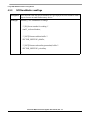
Chapter 2 Abbreviations, Acronyms, and References
2.1
2.2
Abbreviations, Acronyms ................................................................................................ 2-1
References........................................................................................................................ 2-2
Chapter 3 Architecture Overview
3.1
3.2
Old NAND Flash Architecture ........................................................................................ 3-1
New Architecture with Wear Leveling – WL Capability ................................................ 3-3
Chapter 4 Using MQX NAND Flash Wear Leveling Module
4.1
4.2
4.2.1
4.2.2
4.2.3
4.2.4
4.2.5
4.2.6
4.2.7
4.2.8
4.2.9
4.2.10
4.3
4.3.1
4.3.2
4.3.3
4.3.4
4.3.5
4.3.6
4.3.7
4.3.8
4.3.9
Configure Pre-defined Data Drive Layout....................................................................... 4-1
NAND Flash WL API...................................................................................................... 4-3
_io_nandflash_wl_install ............................................................................................. 4-3
_io_nandflash_wl_uninstall ......................................................................................... 4-4
_io_nandflash_wl_open ............................................................................................... 4-5
_io_nandflash_wl_close............................................................................................... 4-6
_io_nandflash_wl_read................................................................................................ 4-7
_io_nandflash_wl_write............................................................................................... 4-8
_io_nandflash_wl_ioctl................................................................................................ 4-9
_io_nandflash_wl_internal_read_metadata ............................................................... 4-10
_io_nandflash_wl_internal_read_with_metadata ...................................................... 4-11
_io_nandflash_wl_internal_write_with_metadata..................................................... 4-12
NFC Physical Media Class ............................................................................................ 4-13
NFCNandMedia::NFCNandMedia............................................................................ 4-13
NFCNandMedia::initChipParam ............................................................................... 4-14
NFCNandMedia::readPage........................................................................................ 4-15
NFCNandMedia::writePage....................................................................................... 4-16
NFCNandMedia::eraseBlock..................................................................................... 4-17
NFCNandMedia::eraseMultipleBlocks ..................................................................... 4-18
NFCNandMedia::copyPages ..................................................................................... 4-19
NFCNandMedia::isBlockBad.................................................................................... 4-20
NFCNandMedia::markBlockBad .............................................................................. 4-21
Freescale MQX™ Flash File System User Guide, Rev. 1.4
Freescale Semiconductor
iii
Contents
Paragraph
Number
4.4
4.4.1
4.4.2
4.5
4.6
4.6.1
4.6.2
4.6.2.1
4.6.2.2
4.6.2.3
4.6.2.4
4.6.2.5
Page
Number
Title
Memory Management.................................................................................................... 4-22
mm_alloc ................................................................................................................... 4-22
mm_free ..................................................................................................................... 4-23
WL Debug...................................................................................................................... 4-24
MFS Example User Manual .......................................................................................... 4-25
User Interface............................................................................................................. 4-25
New Shell Commands ............................................................................................... 4-25
“fsopen” Command ............................................................................................... 4-26
“fsclose” Command ............................................................................................... 4-27
“nanderase” Command .......................................................................................... 4-27
“nandrepair” Command ......................................................................................... 4-27
“nanderasechip” Command ................................................................................... 4-27
Chapter 5 MQX Wear Leveling Internal Functionality
5.1
5.2
5.3
Role of WL Module in NAND Driver............................................................................. 5-1
Input and Output of WL Module ..................................................................................... 5-1
Internal Mechanism inside WL Module .......................................................................... 5-2
Chapter 6 MQX Wear Leveling Internal Software Flow
6.1
6.2
6.3
6.4
6.5
6.5.1
6.5.1.1
6.5.1.2
6.5.2
6.5.3
6.5.3.1
Initialize Flow .................................................................................................................. 6-1
Read Sector Flow............................................................................................................. 6-2
Write Sector Flow ............................................................................................................ 6-3
Shutdown Flow ................................................................................................................ 6-5
Zone Map, Physical Map, and Non-sequential Sector Map Structure............................. 6-5
Phy Map....................................................................................................................... 6-7
Phy Map initialization.............................................................................................. 6-9
Phy Map preservation .............................................................................................. 6-9
Zone Map..................................................................................................................... 6-9
Non-sequential Sector Map ....................................................................................... 6-11
Prevent thrashing when switching from primary block to backup block .............. 6-13
Freescale MQX™ Flash File System User Guide, Rev. 1.4
iv
Freescale Semiconductor
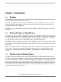
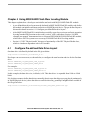
Chapter 1 Introduction
1.1
Purpose
This document describes the architecture of the MQX Wear Leveling module and its interface for the upper
layer such as MFS and Read/Write raw operations.
As a result of significant differences between NAND flash memory and NAND controller in Freescale
CPUs, this document only addresses a Wear Leveling solution for the CPU that is compatible with the
NAND flash memory (NFC hardware).
The MQX Wear Leveling module currently supports all platforms on MQX RTOS that have the NAND
flash device.
1.2
Wearout Problem on Flash Memory
Flash memory is a non-volatile memory that can be easily erased and reprogrammed when compared to
some predecessor memories such as EEPROM. Flash memory is popular as a result of its small physical
size, light weight, low power consumption, high shock resistance, and fast read performance. Currently
there are two types of flash memory: NAND flash memory and NOR flash memory.
NAND flash memory is organized as an array of blocks. Each block contains 32 to 64 pages, where a page
is the smallest unit for read and write operation. On the other hand, to erase, the input must be a block rather
than a pages.
On the other hand, NAND flash memory has a limited number of program/erase cycles (typically known
as P/E cycles). Today the most available flash products in the market are designed to endure around
100,000 P/E cycles before the cells become unreliable. This phenomenon is called memory wear or
wearout.
1.3
Solution to Avoid Wearout Issues
To control the wear-out problem and to extend NAND flash lifetime, a method named wear leveling is
used. Wear leveling tries to distribute every program/erase operations equally on each block in the flash
drive. The equal distribution is done by an internal re-mapping mechanism between logical/physical block
address and writing strategy. The wear leveling writes all new or updated data to a free block, which is
picked from a head of the free block FIFO, then erases the old data block and eventually puts this erased
block to the end of the free block FIFO. This process is done in the background and, for that reason, is
completely transparent to the host system.
Freescale MQX™ Flash File System User Guide, Rev. 1.4
Freescale Semiconductor
1
Introduction
1.4
Outline
The outline of this document is as follows:
• Section 1 – Introduces the purpose of this project and the brief overview of NAND flash memory
and wear leveling.
• Section 2 – Abbreviations and acronyms and reference are used in this document.
• Section 3 – Architecture overview.
• Section 4 – Using MQX NAND Flash Wear Leveling module.
• Section 5 – Functionalities of Wear Leveling module in this project.
• Section 6 – Internal software flow for Wear Leveling module.
Freescale MQX™ Flash File System User Guide, Rev. 1.4
2
Freescale Semiconductor
Chapter 2 Abbreviations, Acronyms, and References
2.1
Abbreviations, Acronyms
Table 2-1. Acronyms and Abbreviations
Acronym
Description
API
Application Programming Interface.
BM
Bare Metal.
HW
Hardware.
IF
Interface.
App
NAND
Application.
In NAND flash memory, users access (read/write) through each page as a minimum unit and erase on
each blocks.
NOR
NOR flash memory lets users be able to random-access in every bytes in flash memory.
Block
A smallest erasable unit in NAND device.
Page
A smallest programmable unit in NAND device.
Physical Block The address of physical block in memory.
Address
(PBA)
Virtual Block Since we used entire flash memory for wear leveling, the VBA is same as LBA. This address points to a
Address
logical address, which are mapped to specific PBA.
(VBA)/Logical
Block Address
(LBA)
Wearout
A circumstance occurs when a block is uneraseable or a page cannot be written.
Wear leveling Wear leveling is a process that helps reduce premature wear in NAND flash devices.
Bad Block
A block resist in NAND flash memories, that cannot be erase or write any more.
Metadata
Data is used by NAND driver to carry a specific information.
Sparedata
An area is typically used for ECC, wear leveling, and other software overhead functions.
NFC
NAND driver
ONFI
Error
Correcting
Code – ECC
NAND Flash Controller.
A driver which is responsible for initializing and handling read/write/erase through NAND memories.
Open NAND Flash Interface.
A code or checksum for automatically correcting purpose. An ECC stores in Metadata/sparedata of each
pages.
Freescale MQX™ Flash File System User Guide, Rev. 1.4
Freescale Semiconductor
Abbreviations, Acronyms, and References
Table 2-1. Acronyms and Abbreviations
Acronym
Description
M53015_Lon Evaluation Board for ColdFire MCF5301X CPU. This board contains 8M x 16 bit NOR flahs memory.
gjing
M54455_Red Evaluation Board for ColdFire MCF5445X CPU. This board contains 02 NOR flash memories (16 MB,
strip
512 KB).
M54418_Mod Evaluation Board for ColdFire MCF5441X CPU. FSOFT uses TWR-MCF5441X for testing purpose, this
elo
board also contains 2Gb NAND flash memory.
2.2
References
Table 2-2. References
Serial No
Document Name
Version
1
MQX RTOS Source Code
4.0.2
2
Freescale MQX™ I/O Drivers User Guide
Rev. 9
3
MCF5441x Reference Manual
Rev. 4
4
K70P256M150SF3RM Reference Manual
Rev. 2
5
K60P144M150SF3RM Reference Manual
Rev. 2
6
Datasheet for 2Gb NAND Flash: 29F2G16AABWP
7
Vybrid Reference Manual
Freescale MQX™ Flash File System User Guide, Rev. 1.4
2
Freescale Semiconductor
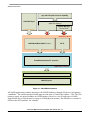
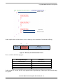
Chapter 3 Architecture Overview
3.1
Old NAND Flash Architecture
The current Freescale MQX NAND flash architecture contains two key components: NAND driver and
NAND Flash Controller – NFC.
• NAND driver: Generally, this driver offers functions such as read, write, erase, raw and IOCTL
operations for upper layer.
• NAND Flash Controller – NFC: This layer providers the NAND HW abstraction, which allows the
hardware independent implementation of higher layers, that is, NAND driver.
The architecture of NAND flash driver in MQX can be seen in the figure below:
Freescale MQX™ Flash File System User Guide, Rev. 1.4
Freescale Semiconductor
1
Architecture Overview
App with Filesystem access capability
Old NAND Apps
MFS
(MQX File System)
Partition Manager
Device Driver
fopen("nandflash:")
X
X
NAND Flash Driver
IOCTL
NAND Read/Write RAW Function
Read/Write/Erase/IOCTL operation
NAND Flash Controller
NAND Flash Controller Hardware
NAND Physical
SoC CPU
Figure 3-1. Old NAND Architecture
All NAND applications could be interactive with NAND flash driver through I/O driver with signature
“nandflash:.” The smallest unit that NAND apps can read/write is Virtual Page Address – VPA. The VPA
points to exactly one physical address on NAND memory. However, a size of each page in NAND
Apps/NAND driver is not the same as a page in NAND physical memory. The difference is a result of a
divider in the NFC hardware. For example:
Freescale MQX™ Flash File System User Guide, Rev. 1.4
2
Freescale Semiconductor
Architecture Overview
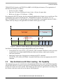
TWR-MCF54418 board uses MT29F2G16AABWP as NAND physical memory. The organization of
NAND in this instance is as follows:
• Device size: 2Gb = 256MB
• Page size: 2112 bytes (2048 bytes for user’s data + 64 bytes for spare data)
• Block size: 64 pages ( 135,168 bytes = 132KB)
By setting up the NFC HW register, the user can logically split the physical page size to a smaller one. This
configuration can be done by modifying NFC_CFG[PAGECNT] register. For example: if we set
NFC_CFG[PAGECNT] to 4, a physical page size will be divided into 4 virtual pages with size 2112B/4 =
528B in each. By doing so, user applications can handle smaller page size easily.
2011B
2047B
0B
Spare data Physical Page 1
Size = 2048B
Size = 64B
Virtual Page 2
Virtual Page 3
Virtual Page 4
2047B+16
B
NFC divide by setting
NFC_CFG[PAGECNT]=4
2047B
511B
0B
Virtual Page 1
Physical Page
Spare
Virtual
page 1
Spare Spare
Virtual Virtual
page 2 page 3
Spare
Virtual
page 4
Figure 3-2. Difference between NAND Physical Organization and Virtual Organization
NAND driver currently does not support MQX MFS because of the follwing:
• Getting Block Size in IO_IOCTL_GET_BLOCK_SIZE command: NAND driver does not return
a correct block size in bytes (MQX MFS needs a block size in bytes, which can be used for
read/write operations).
• Identifying a total sector of storage devices through an IOCTL command
(IO_IOCTL_GET_NUM_SECTORS): Currently, NAND driver does not implement this IOCTL
command.
3.2
New Architecture with Wear Leveling – WL Capability
This solution focuses on a few modifications about MQX NAND flash driver and NAND Flash Controller.
It helps MFS (MQX File System) to run on top of NAND flash memory device and makes NAND flash
memory device not wear out too quickly. This solution also allows the new applications to run along with
the old ones, which are used to access raw data on NAND physical.
Freescale MQX™ Flash File System User Guide, Rev. 1.4
Freescale Semiconductor
3
Architecture Overview
App with Filesystem access capability
fopen("nandflash_wl:"), IOCTL to enable WL
Old NAND Apps
MFS
(MQX File System)
Partition Manager
Device Driver
fopen("nandflash:")
NAND Flash Drivers
Legend
Media manager
Add new
Mapper manager
Old Nandflash
driver with RAW
operations
NandFlash HAL
Modified
NFC Nand Physical Media
No modification
New NandFlash driver with
Wear-Leveling (WL) functions
Old Read/Write/Erase/
IOCTL operation
ReadPage/Write
Page with metadata
Metadata/
Spare Read
operation
NAND Flash Controller
NAND Flash Controller Hardware
NAND Physical
SoC CPU
Figure 3-3. New NAND Architecture with Wear Leveling Capability
In this figure:
• NAND flash driver
— Old NAND flash driver: provides read/write raw function for all legacy applications.
Freescale MQX™ Flash File System User Guide, Rev. 1.4
4
Freescale Semiconductor
Architecture Overview
•
— New NAND flash driver with Wear Leveling: supplies read/write with wear-leveling capability
for upper layers such as MFS.
– Wear Leveling functions: this module contains all mapping mechanisms between Virtual
Page Address and Physical Page Address. It also maintains mapping tables on flash memory
and RAM.
NAND Flash Controller (NFC)
— Read/Write/Erase/IOCTL operation: old NFC’s function for read/write/erase directly with
NFC hardware. These functions work only with Virtual Page data.
— ReadPage/WritePage with metadata: add new function for read/write page’s data and metadata.
— Metadata/Spare Read/Write operation: add new functions for handling spare data, which is
used on Wear Leveling module. These functions simply read/write metadata of each pages
from spare area.
— In this new architecture, organization of virtual pages in physical pages is different with the old
architecture.
Spare data Physical Page 1
Size = 2048B
Size = 64B
511B
+16
511B
0B
NFC divide by setting
NFC_CFG[PAGECNT]=4
Virtual Page 3
Spare
Virtual
page 3
Virtual Page 2
Spare
Virtual
page 2
Virtual Page 1
Spare
Virtual
page 1
Factory Bad Marking at
2048 (Physical Page size)
Spare
Virtual
page 4
2011B
2047B
0B
Virtual Page 4
Physical Page
Figure 3-4. New Organization of Each Virtual Page in Physical Pages
By comparing Figure 3-2 and Figure 3-4, all virtual pages are placed in the reserved order. By doing so,
we can preserve the location of Factory Bad Marking byte of NAND flash.
Freescale MQX™ Flash File System User Guide, Rev. 1.4
Freescale Semiconductor
5
Architecture Overview
Freescale MQX™ Flash File System User Guide, Rev. 1.4
6
Freescale Semiconductor
Chapter 4 Using MQX NAND Flash Wear Leveling Module
This chapter explains how a developer can initialize and work with MQX NAND Flash WL module:
• A pre-defined data driver layout must be declared in MQX NAND Flash WL module code before
this module can initialize and start read/write on NAND physical device. The pre-defined layout is
discussed in detail in section “4.1 Configure pre-defined data drive layout”.
• After MQX NAND Flash WL is initialized successfully; upper layer can issue read/write operation
by using standard FIO function such as read(), write(), seek(), and others. Section “4.6 MFS
example user manual” demonstrates how to cooperate MFS with MQX NAND Flash WL module,
which allows FAT file system to access on top of NAND Flash Wear Leveling module.
• Section “4.3 NFC Physical media” discusses a functionality of the NFC Physical Media class,
which is a hardware dependent code in WL module.
4.1
Configure Pre-defined Data Drive Layout
One data drive is defined by default in the file given below:
<mqx>/source/io/nandflash_wl/nandflash_wl.h>.
Developer can use two macros, as shown below, to configure the start location and size for the first data
drive.
#define NANDFLASH_1ST_DATA_DRIVE_SIZE_IN_BLOCK
#define NANDFLASH_1ST_DATA_DRIVE_START_BLOCK
For example:
#define NANDFLASH_1ST_DATA_DRIVE_SIZE_IN_BLOCK 90
#define NANDFLASH_1ST_DATA_DRIVE_START_BLOCK 110
In this example, the data drive size, in blocks, is 90. This data driver is expanded from 110th to 199th
block.
If a developer wants to define data drivers manually (that is some data drivers are not placed continuously
in NAND physical device), these data drivers can be declared in g_nandZipConfigBlockInfo variable in
the file given below:
<mqx>/source/io/nandflash_wl/wearleveling/hal/ddi_nand_media_defination.cpp.
Freescale MQX™ Flash File System User Guide, Rev. 1.4
Freescale Semiconductor
1
Using MQX NAND Flash Wear Leveling Module
Number of drives
Size of drive
Start block of drive
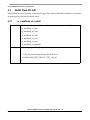
In this sample, there are three drives, two are data type, one is unknown. It means the follwing:
10
1st drive
Data type
(Use to hold data)
0
19
2nd drive
Unknown type
(Unused)
9
3rd drive
Data type
(Use to hold data)
20
99
Figure 4-1. Manually Pre-defined 03 data Drivers
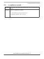
Drives could be the following types:
Enum LogicalDriveType_t
Description
kDriveTypeData
Public data drive
kDriveTypeSystem
System data drive
kDriveTypeHidden
Hidden data drive
kDriveTypeUnknown
Unknown data drive
In the current WL version, the WL only supports kDriveTypeData type. Other types with its block range
are ignored.
Freescale MQX™ Flash File System User Guide, Rev. 1.4
Freescale Semiconductor
2
Using MQX NAND Flash Wear Leveling Module
4.2
NAND Flash WL API
NAND Flash WL driver provides an interface for upper layer such as MFS and read/write raw operations.
Its prototypes are described as shown below.
4.2.1
_io_nandflash_wl_install
Description
This function is responsible for installing the main functions of nandflash memory.
_io_nandflash_wl_open
_io_nandflash_wl_close
_io_nandflash_wl_read
_io_nandflash_wl_write
_io_nandflash_wl_ioctl
_io_nandflash_wl_uninstall
Prototype
_mqx_uint _io_nandflash_wl_install
(
/* [IN] The initialization structure for the device */
NANDFLASH_INIT_STRUCT _PTR_ init_ptr
)
Freescale MQX™ Flash File System User Guide, Rev. 1.4
3
Freescale Semiconductor
Using MQX NAND Flash Wear Leveling Module
4.2.2
_io_nandflash_wl_uninstall
Description
This function is used to uninstall the nandflash memory and free all unused allocated
memory.
Prototype
_mqx_int _io_nandflash_wl_uninstall
(
/* [IN] The IO device structure for the device */
IO_DEVICE_STRUCT_PTR io_dev_ptr
)
Freescale MQX™ Flash File System User Guide, Rev. 1.4
Freescale Semiconductor
4
Using MQX NAND Flash Wear Leveling Module
4.2.3
_io_nandflash_wl_open
Description
This function is used to open and initialize nand flash driver supported wear leveling
feature. Depending on the input argument, the core of the driver is either built or
ignored.
Prototype
_mqx_int _io_nandflash_wl_open
(
/* [IN] the file handle for the device being opened */
MQX_FILE_PTR fd_ptr,
/* [IN] the remaining portion of the name of the device */
char_ptr open_name_ptr,
/* [IN] the flags to be used during operation: */
char_ptr flags
)
Freescale MQX™ Flash File System User Guide, Rev. 1.4
5
Freescale Semiconductor
Using MQX NAND Flash Wear Leveling Module
4.2.4
_io_nandflash_wl_close
Description
This function is used to close nand flash driver.
Prototype
_mqx_int _io_nandflash_wl_close
(
/* [IN] the file handle for the device being closed */
MQX_FILE_PTR fd_ptr
)
Freescale MQX™ Flash File System User Guide, Rev. 1.4
Freescale Semiconductor
6
Using MQX NAND Flash Wear Leveling Module
4.2.5
_io_nandflash_wl_read
Description
Modules of upper layers use this function to read a logical sector from nand flash
memory device via core and NFC Physical media.
Prototype
_mqx_int _io_nandflash_wl_read
(
/* [IN] the file handle for the device */
MQX_FILE_PTR fd_ptr,
/* [IN] where the data is to be stored */
char_ptr data_ptr,
/* [IN] the number of pages to input */
_mqx_int num
)
Freescale MQX™ Flash File System User Guide, Rev. 1.4
7
Freescale Semiconductor
Using MQX NAND Flash Wear Leveling Module
4.2.6
_io_nandflash_wl_write
Description
Modules of the upper layers use this function to write a logical sector from nand flash
memory device via core and NFC Physical media.
Prototype
_mqx_int _io_nandflash_wl_write
(
/* [IN] the file handle for the device */
MQX_FILE_PTR fd_ptr,
/* [IN] where the data is stored */
char_ptr data_ptr,
/* [IN] the number of pages to output */
_mqx_int num
)
Freescale MQX™ Flash File System User Guide, Rev. 1.4
Freescale Semiconductor
8
Using MQX NAND Flash Wear Leveling Module
4.2.7
_io_nandflash_wl_ioctl
Description
This function contains a useful control command to communicate with low layer
hardware.
Prototype
_mqx_int _io_nandflash_wl_ioctl
(
/* [IN] the file handle for the device */
MQX_FILE_PTR fd_ptr,
/* [IN] the ioctl command */
_mqx_uint cmd,
/* [IN/OUT] the ioctl parameters */
pointer param_ptr
)
Freescale MQX™ Flash File System User Guide, Rev. 1.4
9
Freescale Semiconductor
Using MQX NAND Flash Wear Leveling Module
4.2.8
_io_nandflash_wl_internal_read_metadata
Description
This function is responsible to read only data of the spare area. It’s called from
_io_nandflash_wl_ioctl function by the input command.
Prototype
_mqx_int _io_nandflash_wl_internal_read_metadata
(
/* [IN] the file handle for the device */
MQX_FILE_PTR fd_ptr,
/* [IN] where the data is to be stored */
char_ptr data_ptr,
/* [OUT] the error is returned */
uint_32_ptr ret_err
)
Freescale MQX™ Flash File System User Guide, Rev. 1.4
Freescale Semiconductor
10
Using MQX NAND Flash Wear Leveling Module
4.2.9
_io_nandflash_wl_internal_read_with_metadata
Description
This function is used to read all data in a sector. It’s called from
_io_nandflash_wl_ioctl function by the input command.
Prototype
_mqx_int _io_nandflash_wl_internal_read_with_metadata
(
/* [IN] the file handle for the device */
MQX_FILE_PTR fd_ptr,
/* [IN] where the data is to be stored */
char_ptr page_struct_ptr,
/* [IN] the number of pages to input */
_mqx_int num,
/* [OUT] the error is returned */
uint_32_ptr ret_err
)
Freescale MQX™ Flash File System User Guide, Rev. 1.4
11
Freescale Semiconductor
Using MQX NAND Flash Wear Leveling Module
4.2.10
_io_nandflash_wl_internal_write_with_metadata
Description
This function is used to write data to a sector, and metadata in the spare area.
Prototype
_mqx_int _io_nandflash_wl_internal_write_with_metadata
(
/* [IN] the file handle for the device */
MQX_FILE_PTR fd_ptr,
/* [IN] where the data is stored */
char_ptr page_buff_struct,
/* [IN] the number of pages to output */
_mqx_int num,
/* [OUT] the error is returned */
uint_32_ptr ret_err
)
Freescale MQX™ Flash File System User Guide, Rev. 1.4
Freescale Semiconductor
12
Using MQX NAND Flash Wear Leveling Module
4.3
•
NFC Physical Media Class
NFC Physical Media class, which is a subclass of the NandPhysicalMedia abstract class, is a
hardware dependent code that is responsible for bridging between WL module and specific
hardware NAND Flash Controller (NFC). This class prototype is discussed in detail in subsequent
section.
NOTE
WL can support a new NAND Flash Controller (that is CPU does not have NFC hardware) by simply
creating a new class, which is based on NandPhysicalMedia, and initializing it properly in NandHal class.
NFC physical media is located as shown below:
<mqx>/source/io/nandflash_wl/wearleveling/hal/ddi_nand_hal_nfcphymedia.cpp.
4.3.1
NFCNandMedia::NFCNandMedia
Description
This is a constructor of the NFC Physical media module.
Prototype
NFCNandMedia::NFCNandMedia
(
/* [IN] chip number for enabling */
uint32_t chipNumber
)
Freescale MQX™ Flash File System User Guide, Rev. 1.4
13
Freescale Semiconductor
Using MQX NAND Flash Wear Leveling Module
4.3.2
NFCNandMedia::initChipParam
Description
This function initializes all chip parameters such as pages per block, page size, etc.
Prototype
void NFCNandMedia::initChipParam()
Freescale MQX™ Flash File System User Guide, Rev. 1.4
Freescale Semiconductor
14
Using MQX NAND Flash Wear Leveling Module
4.3.3
NFCNandMedia::readPage
Description
This function reads data and its metadata on a given physical sector number# from a
physical sector in nand flash memory device.
Prototype
RtStatus_t NFCNandMedia::readPage
(
/* [IN] Sector number for reading */
uint32_t uSectorNumber,
/* [OUT] Return read data buffer */
SECTOR_BUFFER * pBuffer,
/* [OUT] Return read auxiliary(metadata) buffer */
SECTOR_BUFFER * pAuxiliary
)
Freescale MQX™ Flash File System User Guide, Rev. 1.4
15
Freescale Semiconductor
Using MQX NAND Flash Wear Leveling Module
4.3.4
NFCNandMedia::writePage
Description
This function reads data and its metadata on given physical sector number# from a
physical sector in the nand flash memory device.
Prototype
RtStatus_t NFCNandMedia::readPage
(
/* [IN] Sector number for reading */
uint32_t uSectorNumber,
/* [OUT] Return read data buffer */
SECTOR_BUFFER * pBuffer,
/* [OUT] Return read auxiliary(metadata) buffer */
SECTOR_BUFFER * pAuxiliary
)
Freescale MQX™ Flash File System User Guide, Rev. 1.4
Freescale Semiconductor
16
Using MQX NAND Flash Wear Leveling Module
4.3.5
NFCNandMedia::eraseBlock
Description
This function is used to erase a given physical block number#.
Prototype
RtStatus_t NFCNandMedia::eraseBlock
(
/* [IN] Given block for erase request */
uint32_t uBlockNumber
)
Freescale MQX™ Flash File System User Guide, Rev. 1.4
17
Freescale Semiconductor
Using MQX NAND Flash Wear Leveling Module
4.3.6
NFCNandMedia::eraseMultipleBlocks
Description
This function is used to erase a range of physical blocks.
Prototype
RtStatus_t NFCNandMedia::eraseMultipleBlocks
(
/* [IN] Start block No# for erase request */
uint32_t startBlockNumber,
/* [IN] Number of block for erase request */
uint32_t requestedBlockCount,
/* [OUT] Actual erased block */
uint32_t * actualBlockCount
)
Freescale MQX™ Flash File System User Guide, Rev. 1.4
Freescale Semiconductor
18
Using MQX NAND Flash Wear Leveling Module
4.3.7
NFCNandMedia::copyPages
Description
This function is used to copy data of multiple physical sectors (data and metadata)
from a source device to a target device.
Prototype
RtStatus_t NFCNandMedia::copyPages
(
/* [IN] Target Nand is request for copy to */
NandPhysicalMedia * targetNand,
/* [IN] Start from sector No# */
uint32_t wSourceStartSectorNum,
/* [IN] Copy to target's sector No# */
uint32_t wTargetStartSectorNum,
/* [IN] Number of sector for copying */
uint32_t wNumSectors,
/* [IN] The temporary sector buffer */
SECTOR_BUFFER * sectorBuffer,
/* [IN] The temporary auxilary buffer */
SECTOR_BUFFER * auxBuffer,
/* [IN] For copy filtering purpose */
NandCopyPagesFilter * filter,
/* [OUT] Actual number of copied pages */
uint32_t * successfulPages
)
Freescale MQX™ Flash File System User Guide, Rev. 1.4
19
Freescale Semiconductor
Using MQX NAND Flash Wear Leveling Module
4.3.8
NFCNandMedia::isBlockBad
Description
This function checks whether a given block is bad.
Prototype
bool NFCNandMedia::isBlockBad
(
/* [IN] Given block No# */
uint32_t blockAddress,
/* [IN] The temporary sector buffer */
SECTOR_BUFFER * auxBuffer,
/* [IN] Indicate whether we should check the factory marking position,
** NFCNandMedia currently does implement in lower layer
*/
bool checkFactoryMarkings,
/* [OUT] Read status */
RtStatus_t * readStatus
)
Freescale MQX™ Flash File System User Guide, Rev. 1.4
Freescale Semiconductor
20
Using MQX NAND Flash Wear Leveling Module
4.3.9
NFCNandMedia::markBlockBad
Description
This function is used to mark a block as bad.
Prototype
RtStatus_t NFCNandMedia::markBlockBad
(
/* [IN] Given block No# */
uint32_t blockAddress,
/* [IN] The temporary sector buffer */
SECTOR_BUFFER * pageBuffer,
/* [IN] The temporary sector auxiliary buffer */
SECTOR_BUFFER * auxBuffer
)
Freescale MQX™ Flash File System User Guide, Rev. 1.4
21
Freescale Semiconductor
Using MQX NAND Flash Wear Leveling Module
4.4
Memory Management
Memory management is a useful module to manage/profile allocated memory. It enables both the
developer and the user to know the amount of allocated/free and leaked memory.
This module can be easily turned off by changing the definition: NANDWL_MEM_LEAK_DETECTION
to zero. When the definition is zero, the NAND Flash WL module uses MQX standard allocator/free
memory – mem_alloc()/free() function instead of NAND Flash WL’s function – mm_alloc()/mm_free().
This memory management module is located as shown below:
<mqx>/source/io/nandflash_wl/wearleveling/rtos/mqx/mem_management.cpp.
4.4.1
mm_alloc
Description
This function allocates a buffer with a given size. Each buffer includes two
signatures, at head and tail, to trace their status. To manage memory, it’s better to
implement this function, in place of using standard functions.
Prototype
pointer mm_alloc
(
/* [IN] size of requested buffer */
_mem_size request_size,
/* [IN] file name which requests buffer */
const char* file_name,
/* [IN] Location in file_name */
int file_loc,
/* [IN] Should zero buffer after allocated */
boolean isZero,
/* [IN] Is this buffer requested from new operator */
boolean is_from_operator
)
Freescale MQX™ Flash File System User Guide, Rev. 1.4
22
Freescale Semiconductor
Using MQX NAND Flash Wear Leveling Module
4.4.2
mm_free
Description
This function is used to free allocated memory. It will check the signature included
and alert invalid allocated buffer.
Prototype
_mqx_uint mm_free
(
/* [IN] pointer to head of allocated buffer */
pointer buf
)
Freescale MQX™ Flash File System User Guide, Rev. 1.4
Freescale Semiconductor
23
Using MQX NAND Flash Wear Leveling Module
4.5
WL Debug
WL Debug is designed to support developers to debug each sub module or all sub modules of the NAND
Flash WL core. If a debug module is enabled, all messages of verbose module will be printed out by using
WL_LOG statement. The syntax is shown below:
WL_LOG(<WL_Module>, <Log_type>, <Message>);
Disabled debug module
Enabled debug modules
This module is located as shown below:
<mqx>/source/io/nandflash_wl/wearleveling/wl_common.cpp.
Freescale MQX™ Flash File System User Guide, Rev. 1.4
24
Freescale Semiconductor
Using MQX NAND Flash Wear Leveling Module
4.6
4.6.1
MFS Example User Manual
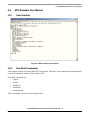
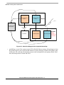
User Interface
Figure 4-2. MFS example user interface
4.6.2
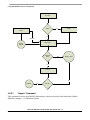
New Shell Commands
This example is based on existing MFS SD Card example. Therefore, it has common shell commands and
some new commands, which are only used for FFS.
New shell commands are:
• fsopen
• fsclose
• nanderase
• nandrepair
• nanderasechip
These commands are shown in the diagram below:
Freescale MQX™ Flash File System User Guide, Rev. 1.4
Freescale Semiconductor
25
Using MQX NAND Flash Wear Leveling Module
WL Open
Failed
Yes
Repair
Erase
No
Try again
MFS Open
Unknow
ERROR
Not DOS
DISK
No
Ready to USE
Yes
Format
No
ERROR
4.6.2.1
No
Success
“fsopen” Command
This command is used to open NAND flash memory with wear leveling. Each sub module (Media,
DataDrive, Mapper…) is initialized in order.
Freescale MQX™ Flash File System User Guide, Rev. 1.4
26
Freescale Semiconductor
Using MQX NAND Flash Wear Leveling Module
4.6.2.2
“fsclose” Command
This command is used to close NAND flash memory and shutdown initialized wear leveling module.
4.6.2.3
“nanderase” Command
This command is used to erase all blocks, which are defined as Data drive. These blocks are erased by wear
leveling module, not NFC directly.
4.6.2.4
“nandrepair” Command
This command is used to repair all blocks in defined Data drive. Random data will be written to these
blocks (included the spare area) and their status is also checked. The wear leveling module will rebuild
necessary maps because they were erased while the Data drive is being repaired.
4.6.2.5
“nanderasechip” Command
This command is used to erase all blocks in NAND flash memory. These blocks are erased directly by the
NFS ioctl. The wear leveling module is not installed.
NOTE
•
•
First time users of the MFS NAND Flash example, should run “nanderasechip” command first. If
the data in the spare area, which holds metadata of each sector, is cluttered, it will cause the core
to malfunction. With incorrect data, the core will build incorrect maps and critical errors may occur.
To change the size of the default data drive or the structure of the NAND media, please make sure
they were declared in g_nandZipConfigBlockInfo variable.
Freescale MQX™ Flash File System User Guide, Rev. 1.4
Freescale Semiconductor
27
Using MQX NAND Flash Wear Leveling Module
Freescale MQX™ Flash File System User Guide, Rev. 1.4
28
Freescale Semiconductor
MQX Wear Leveling Internal Functionality
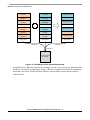
Chapter 5 MQX Wear Leveling Internal Functionality
This section describes the functionalities of Wear Leveling module in NAND flash driver.
5.1
Role of WL Module in NAND Driver
This module is mainly responsible for mapping from a virtual page address to a physical page address. By
doing so, the wear leveling works transparently with the upper layer such as MQX MFS. Applications in
the upper layer pass a logical sector (or virtual page address) to WL’s module resists inside NAND driver.
After that, the WL mechanism searches its internal mapping table on RAM or flash memory to find the
desired physical page address.
There are a few existing mapping tables, namely PhyMap, ZoneMap, and NonSequentialSectorMap,
maintained in the WL module. In the initialization step, WL tries to build up the PhyMap and ZoneMap
by scanning all blocks in the reserved area on NAND physical to find the suitable map structure.
NonSequentialSectorMap is built from metadata in every physical page.
If NAND memory is fresh or does not contain WL information, these maps will initialize with default
parameters. On each read/write operation from the upper layer, these maps will update by getting rid of a
non-existing entry and fetching a new one from the flash memory. Finally, when upper layer closes the
flash driver, all map data will be flushed to the physical pages encapsulated in a special structure.
In addition, WL map retains all good blocks and bad blocks on NAND flash memory. If WL catches an
error related to the writing or erasing operation on a specific block, it marks the block as bad and avoids it
in the future allocation.
5.2
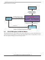
Input and Output of WL Module
The following figure depicts WL input and output parameters that are passed between each module and
function.
Freescale MQX™ Flash File System User Guide, Rev. 1.4
Freescale Semiconductor
1
MQX Wear Leveling Internal Functionality
Application/Upper layer
Read/Write on specific
Logical Sector Address
used on file system
Call NAND Read/Write raw on
calculated
Physical Page Address
NAND Read/Write
raw functions
WL module
Calculate Logical Sector Address (Virtual
Page Address) Physical Page Address
Get Metadata from page’s Spare area
Read/Write raw
NFC
Figure 5-1. Input/Ouput Parameters of WL Module
5.3
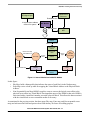
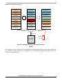
Internal Mechanism inside WL Module
The most important task for WL module is to get essential information from maps or flash memory and
calculate the physical page address from Logical Sector/Page Address to Physical Page Address. To do so,
WL must cooperate with maps as shown in the figure below:
Freescale MQX™ Flash File System User Guide, Rev. 1.4
2
Freescale Semiconductor
MQX Wear Leveling Internal Functionality
NAND Read/
Write raw
MFS/Upper layer
Read/Write raw
A logical sector address
used on file system
WL Module
Get metadata
NFC
WL Module
Logical sector
address
Mathematical convert
Virtual sector
address
Virtual sector
offset
Not found on Map
Get FREE block
Phy map
return FREE block
Zone map
Look up
block
Virtual block
address
Look up
page
Physical block
address
Nonsequential
Sector Map
Physical sector
offset
Physical sector
address
Figure 5-2. Internal Mechanism inside WL Module
In this figure:
• Phy Map: holds a bitmap table that indicates the status of each block in the flash memory.
• Zone Map: stores a look up table for mapping the Vritual Block Address to the Physical Block
Address.
• Non-Sequential Sector Map (NSSM): supplies a map to convert the logical sector offset to the
physical sector offset in a Virtual Block. One important aspect of the NSSM is that each NSSM is
associated with a virtual block number, not with a physical block. This allows the data associated
with the virtual block to move around the media as necessary.
As mentioned in the previous section, the three maps (Phy map, Zone map, and Non-sequential sector
map) are both stored in RAM and preserved on flash memory for future re-building purpose.
Freescale MQX™ Flash File System User Guide, Rev. 1.4
Freescale Semiconductor
3
MQX Wear Leveling Internal Functionality
Freescale MQX™ Flash File System User Guide, Rev. 1.4
4
Freescale Semiconductor
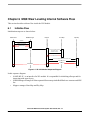
Chapter 6 MQX Wear Leveling Internal Software Flow
This section describes software flow inside the WL Module.
6.1
Initialize Flow
Initialization steps are as shown below:
NAND WL IF
NSSM Manager
Mapper
Zone Map
Phy Map
Initialize
Initialize successfully
Initialize failed
Initialize
Load or scan and build from NAND
Flash memory device
Load/Build successfully
Load/Build failed
Load or scan and build from NAND Flash memory device
Load/Build successfully
Load/Build failed
Initialize failed
Figure 6-1. WL Initialization Sequence Diagram
In this sequence diagram:
• NAND WL IF : is an interface for WL module. It is responsible for initializing all maps and for
interacting with upper layers.
• NSSM Manager: manages all Non-sequential Sector maps in the Red Black tree structure and LRU
list.
• Mapper: manages Zone Map and Phy Map.
Freescale MQX™ Flash File System User Guide, Rev. 1.4
Freescale Semiconductor
1
MQX Wear Leveling Internal Software Flow
6.2
Read Sector Flow
Virtual Block Number
Logical Sector
Number
Zone Map + Phy Map
Relative Physical
Block Number
Mathematical
Converter
Physical Sector
Number
Virtual Block Number
Virtual Sector Offset
Non-sequential Sector
Map of the virtual
block
Relative Physical
Sector Offset
Figure 6-2. WL Read Sector Flow
NAND WL IF
Logical Sector
Number
Zone Map
Get relative Physical Block Number
of Virtual Block Number
of Logical Sector Number
Phy Map
Non‐sequential Sector Map
Assign a new free physical block
if does not find out
Return 0xFF buffer when can’t get
relative Physical Block
Return a new free
Physical Block Number
Return the relative
Physical Block Number
Get Physical Sector Offset of Virtual Sector Number
of Logical Sector Number within the relative Physical Block Number
There is something wrong
Return relative Physical Sector Offset
Physical
Sector Number
Figure 6-3. WL Read Sector Sequence Diagram
In this sequence diagram:
• Step 1: If MFS wants to read data from a logical sector, it passes a logical sector address to the
NAND WL IF of the NAND driver. WL needs to make sure that a given logical sector is not out
of bounds.
• Step 2: The NAND WL IF converts the input logical sector number mathematically into a virtual
block number and a virtual block offset.
• Step 3: If the Zone map object is loaded or built from the initialization phase, the NAND WL IF
searches the map to figure out a relative physical block of this virtual block. If the physical block
cannot be found, that means that no physical block was assigned to this virtual block, and that a
Freescale MQX™ Flash File System User Guide, Rev. 1.4
2
Freescale Semiconductor
MQX Wear Leveling Internal Software Flow
•
•
6.3
free physical block that is available in Phy map is assigned and a buffer filled with 0xFF sent back
to MFS.
Step 4: The NAND WL IF scans all entries in Non-sequential Sector Map of the virtual block to
get location (offset) of the virtual sector in the block which it belongs to. If the Non-sequential
Sector Map was not loaded to SDRAM, each sector of the relative physical sector is scanned to
read metadata and Non-sequential Sector Map is built.
Step 5: If WL has the physical sector number and the physical sector offset number, it knows
exactly which physical sector must be sent to the NFC. However, WL also needs to confirm
whether the sector is written or not. If it is not written, it returns an 0xFF buffer.
Write Sector Flow
Virtual Block Number
Logical Sector
Number
Zone Map + Phy Map
Relative Physical
Block Number
Mathematical
Converter
Available Physical
Sector Number
Virtual Block Number
Virtual Sector Offset
Non-sequential Sector
Map of the virtual
block
The next
available Physical
Sector Offset
Figure 6-4. WL Write Sector Flow
Freescale MQX™ Flash File System User Guide, Rev. 1.4
3
Freescale Semiconductor
MQX Wear Leveling Internal Software Flow
NAND WL IF
Logical Sector
Number
Zone Map
Get relative Physical Block Number
of Virtual Block Number
of Logical Sector Number
Phy Map
Non‐sequential Sector Map
Assign a new free physical block
if does not find out
Return 0xFF buffer when can’t get
relative Physical Block
Return a new free
Physical Block Number
Return the relative
Physical Block Number
Get the next available Physical Sector Offset of Virtual Sector Number
of Logical Sector Number within the relative Physical Block Number
There is something wrong
Return suitable Physical Sector Offset
Physical
Sector Number
Update Non-sequential Sector Map
Figure 6-5. WL Write Sector Sequence Diagram
In this sequence diagram:
• Step 1: If the MFS wants to write data to a logical sector, it transfers a logical sector address to the
NAND WL IF of the NAND driver. WL needs to make sure that a given logical sector is not out
of bounds.
• Step 2: The NAND WL IF converts the input logical sector number mathematically into a virtual
block number and a virtual block offset.
• Step 3: If the Zone map object is loaded or built from the initialization phase, the NAND WL IF
searches the map to figure out the relative physical block of this virtual block. If the physical block
cannot be found, that means that no physical block is assigned to this virtual block, and that a free
physical block, which is available in Phy map, is assigned.
• Step 4: The NAND WL IF scans all entries in the Non-sequential Sector Map of the virtual block
to get location (offset) of the next available virtual sector in the block to which it belongs. If the
Non-sequential Sector Map was not loaded to SDRAM, each sector of the relative physical sector
is scanned to read metadata and Non-sequential Sector Map is built later.
• If the next available virtual sector is out of bounds because the physical block is full, WL marks
that physical block as a backup block and gets a new free block to write data. Old backup block
needs to be erased and marked as free.
• Step 5: If WL has the physical sector number and the physical sector offset number, WL knows
exactly which physical sector must be sent to the NFC. However, if an error occurs when writing
and the NFC cannot fix that error, WL has to copy content of the physical block to another free
block and mark the previous block as bad. The NFC continues writing on the new block.
Freescale MQX™ Flash File System User Guide, Rev. 1.4
4
Freescale Semiconductor
MQX Wear Leveling Internal Software Flow
•
6.4
Step 6: After the NFC writes successfully, the Non-sequential Sector Map of the physical block
needs to be updated.
Shutdown Flow
Figure 6-6. WL Shutdown/Flush Sequence Diagram
Before releasing all variable that is allocated on memory, WL needs to flush all Non-sequential Sector
Maps by merging the backup block and the primary block to free the unused block, and write Zone map
and Phy map on NAND flash memory device if they are not saved.
6.5
Zone Map, Physical Map, and Non-sequential Sector Map
Structure
Zone Map and Physical Map are organized inside the flash memory as shown in the figure below:
Freescale MQX™ Flash File System User Guide, Rev. 1.4
5
Freescale Semiconductor
MQX Wear Leveling Internal Software Flow
Reserved Block Area
Zone Map Block
All data & spare are 0xFF
indicate this page is FREE
Persistent Phy Map Block
FREE
FREE
FREE
User Block
User Block
Page 0
First LBA
FREE
Page 1
FREE
Page 2
Section 1
Page 3
Section 2
Page 4
Section 3
Page 5
Section 4
Header contains
Signature,
totalEntries,
firstLBA
User Block
Entry
2nd
Entry
totalEn
tries-th
Entry
3rd
Spare –
generally
unused
A Page (or Section)
organization
User Block
User Block
Entry
1st
top section page Idx
A Map Block
Organization
User Block
User Block
NAND Flash memory
Figure 6-7. Zone Map and Phy Map Organization in Flash Memory
Maps are located in a Reserved Area Block that the user’s data cannot touch. Each map occupies one block
and the others are backups. One map block contains multiple sections that are spread continuously in
virtual pages on the flash memory. To slow down the premature wear-out on this map block, whenever WL
adds new section number to flash memory, it always writes to the first available virtual page (indicated by
top section page index). By using this strategy, WL regularly touches all virtual pages in this block.
Every section contains a header on the first page data. The most important fields in each header are:
• Signature: for identifying a Zone Map or Phy Map
• firstLBA: Logical Block Address of first entry
• totalEntries: total number of entries in this section
The assumption is that, with one physical block (64*4 virtual pages, 512 byte in each page), it is possible
to preserve all mapping information for physical NAND memory. For example:
• For storing Phy Map:
— Virtual page size = 512 bytes and a block contains 64*4 virtual pages
— Section header = 24 bytes
— 02 bits are used for indicating a block’s status
— A block can present status of maximum ((512 bytes-24 bytes)*8bit)/(2 bit) * 64*4 pages =
499,712 blocks (~ 499,712 * 128KB in each block = 61GB NAND flash device)
• For storing Zone Map:
— Virtual page size = 512 bytes and a block contains 64*4 virtual pages
— Section header = 24 bytes
— Each entries contain a 24-bit physical block address
Freescale MQX™ Flash File System User Guide, Rev. 1.4
6
Freescale Semiconductor
MQX Wear Leveling Internal Software Flow
— A block can hold a maximum of ((512 bytes-24 bytes)*8bit)/(24 bit) * 64*4 pages = 41,642
physical block address (~ 41,642 * 128KB in each block = 5GB NAND flash device)
NOTE
When the top section page index reaches the total virtual page in a block
(64*4), it means that this map block is completely full. WL relocates this
block to the new one (still in reserved area block). This process is called
consolidation.
Compared to the Zone and Phy Map, a Non-sequential Sector map is distributed in every virtual page spare
area.
In case NFC_CFG[PAGECNT]=4, we have 64*4 virtual
pages in one block
Virtual Page 0
Block
status
(Non-0xff
= BAD) (1
byte)
Virtual Page 0
Reserved
– use in
case
16bit
Nandflas
h (1 byte)
Logical
Block
Address
(3 bytes)
...
Logical
Sector
Index (2
bytes)
Virtual Page
63*4
Flags
indicates
that all
pages in
the block
are sorted
logically(1
byte)
Spare
Virtual
page 0
Spare
Virtual
page 1
...
Spare
Virtual
page
63
In case ECC uses 8 bytes
for 04bits auto correctiion
ECC
(8bytes)
Figure 6-8. Organization of Non-sequential Sector Map in Virtual Page Spare Area
NOTE
Generally, the reserved block area (RBA) is expandable if there are bad blocks inside this area. In this
instance, the reserved block area moves toward the higher block address and relocates any non-map blocks
which reside in RBA.
6.5.1
Phy Map
Phy map is responsible to get/set a status of the specific physical block. It stores the status of each block
in the flash memory by using a bitmap entry. Each entry in this map uses 01 bit to represent three different
states of a block:
• Block is used (occupied or bad)
• Block is free
Freescale MQX™ Flash File System User Guide, Rev. 1.4
7
Freescale Semiconductor
MQX Wear Leveling Internal Software Flow
Block 1
Used
Block 3
Free
SECTION 2
Block 2
Free
Virtual Page 1
Block 4
Bad
Current Idx Pos++
Block N
Used
SECTION 1
Virtual Page 2
SECTION 3
Used 01 bit for
each entries.
(used/free and
bad/good block)
These entries are encapsulated with a
header and write to NEXT available
virtual page in specific PhyMap block.
Each Virtual page (section) will store
MAX_ENTRIES_PER_PAGE entries.
top section page Idx
Virtual Page 3
Block stores PhyMap
FREE
Blocks
Phy bitmap
entries
NAND Flash memory
Index of Section contains entry for LBAi =
LBAi / Total Entries Per Section
Figure 6-9. Phy Map Organization in Memory and Flash
In this figure:
• Each Physical Virtual Page stores a maximum of MAX_ENTRIES_PER_PAGE entries. WL
encapsulates these entries into a section by padding a header before flushing to flash memory.
• Current index position indicates that the next free non-map block can be allocated. This position is
helpful whenever a user wants to request a new block for writing.
• Top section page index indicates the section of the next free virtual page that can be stored. This
index continuously increments toward the higher address; when it reaches a total page number, WL
will consolidate all sections of this map into the next free block in RBA.
NOTE
A trust number (TN), informs that all maps have been flushed into the flash memory successfully. It is
located in the last two bytes of metadata (byte 7 and byte 8) of every map block. Normally, the TN in Zone
and Phy maps should be as follows:
• TNZoneMap = 16 bit random number
• TNPhyMap = TNZoneMap + 1 (the Phy Map is always written to NAND flash before ZoneMap)
Freescale MQX™ Flash File System User Guide, Rev. 1.4
8
Freescale Semiconductor
MQX Wear Leveling Internal Software Flow
6.5.1.1
Phy Map initialization
Normally, WL checks the trust number to find out whether all maps have been flushed. If so, WL will scan
all blocks in RBA in flash memory to locate the block that holds the PhyMap table during initialization
phase. A valid PhyMap Block should have a valid signature and a consistent structure on each page. If WL
does not find a good Phy Map block, it scans all blocks to build a new one.
6.5.1.2
Phy Map preservation
Whenever the Phy Map changes, (it is dirty),WL flushes it to the flash memory.
6.5.2
Zone Map
Zone map contains a mapping table between Logical Block Address and Physical Block Address.
Logical Block 1
Physical Block 1
Logical Block 2
Physical Block 2
Logical Block 3
Physical Block 3
...
...
Logical Block N
Physical Block N
Logical NAND Flash
memory
Physical NAND Flash
memory
Figure 6-10. Zone Map - Mapping Table between Logical Block Address and Physical Block Address
WL splits this map into many sections and writes to flash memory. Each section contains entries whereby
each entry stores 16 or 24 bits physical block address.
Freescale MQX™ Flash File System User Guide, Rev. 1.4
9
Freescale Semiconductor
MQX Wear Leveling Internal Software Flow
Figure 6-11. Zone Map Organization In memory and Flash
WL maintains this map in flash memory the same way as it does the Phy Map. However, it is difficult to
load the entire Zone Map to memory beacause of the limited RAM . As a result, only some sections of the
zone map are loaded into a cache array for fast look up. If the cache array is full, WL uses the Least
Recently Used (LRU) strategy to remove and fetch a new one from flash memory.
Freescale MQX™ Flash File System User Guide, Rev. 1.4
10
Freescale Semiconductor
MQX Wear Leveling Internal Software Flow
Cache Array which stores n Section of Zone
map wil be filled until it is full.
Section 1
Newer MRU section
Section 2
(The 1st used section)
Most Recently Used
(MRU) section in
SDRAM
Section 3
(up-to-date)
Other section in
SDRAM
3. update to new MRU section
...
Cache miss -> 1. evict
...
Section N-1
(The 2nd used section)
2. fetch
(LRU) section in
SDRAM
Section N
RAM
Zone Map in Flash
memory
Figure 6-12. Cache Array for Zone Map
6.5.3
Non-sequential Sector Map
The Non-sequential sector map (NSSM) is responsible for tracking the block's logical sectors within the
physical location of a block. It also manages the mechanism which updates the block contents in an
efficient manner. All upper layer sectors reading and writing must utilize a non-sequential sector map to
either find the physical location of a logical sector, or to get the page where a new sector should be written.
The NSSM is composed of two key components. First, it has a map which explains the relationship of the
logical sector to a physical page within a block. This allows logical sectors to be written to the block in
any order, which is important for ensuring that pages are only written sequentially within the block as
required by NAND. The map also enables logical sectors to be written to the block more than once, with
the most recent copy taking precedence.
The second element is a backup block. The backup block contains previous contents of the block and
allows only new sectors to be written to the primary block. If a logical sector is not present in the primary
block, it can be read from the backup block. When the primary block becomes full, the primary and backup
are merged into a new block. Merging takes the most recent version of each logical sector from either the
primary or backup and writes it to the new block.
Another important aspect of the NSSM is that each NSSM is associated with a virtual block number, not
a physical block. This allows the data associated with the virtual block to move around on the media as
necessary.
Freescale MQX™ Flash File System User Guide, Rev. 1.4
11
Freescale Semiconductor
MQX Wear Leveling Internal Software Flow
Logical Sector 1
Physical Sector 1
Logical Sector 2
Physical Sector 2
Logical Sector 3
Physical Sector 3
...
...
Logical Sector N
Physical Sector N
Logical Block
Physical Block
Figure 6-13. Mapping between Logical Sector <-> Physical Sector
Each block holds a non-sequential map in the spare area of every page. Whenever upper layer requests to
read or write on a given sector, WL will calculate a virtual block that contains a sector. After that, WL
scans the spare area of all pages of this virtual block to build up a non-sequential sector map.
To boost performance, WL uses specific caching mechanism to improve speed when looking up a logical
sector in one block. Similar to Zone Map, only a few maps are loaded into memory. WL uses LRU strategy
for every cache-missed map. In addition, to enhance the search time, a Red-black tree is used to hold the
non-sequential maps. Each node of the tree is a non-sequential map whereby the key is related to the
Virtual Block Address (VBA) of that map. Since a Red-black tree is a self-balancing binary search tree,
searching-time is optimized.
Freescale MQX™ Flash File System User Guide, Rev. 1.4
12
Freescale Semiconductor
MQX Wear Leveling Internal Software Flow
ROOT
NSSMap for
VBA 13
NSSMap
for VBA
17
NSSMap
for VBA 8
NSSMap
for VBA
11
NSSMap
for VBA 1
NSSMap
for VBA 6
NILL
NILL
NILL
NSSMap
for VBA
15
NILL
NILL
NSSMap
for VBA
25
NILL
NILL
NILL
NILL
Figure 6-14. Non-sequential Map in Red Black Tree Structure
6.5.3.1
Prevent thrashing when switching from primary block to backup block
Since NSSM uses a backup block that contains the previous contents of the block (primary one), when the
primary block becomes full, the primary and backup are merged into a new block. There are a few existing
merge strategies as described below:
• shortCircuitMerge: When the primary block is full, WL requests a new free physical block from
the PhyMap and assigns it as a new primary block. The backup block is erased and freed. At this
time, the backup block points to the previous primary block.
Freescale MQX™ Flash File System User Guide, Rev. 1.4
13
Freescale Semiconductor
MQX Wear Leveling Internal Software Flow
Mapped to
A. Before
m
Physical Primary
Block
fro
Physical Backup
Block
ue
st
a
n
P h ew
y fre
M e
a p bl
oc
k
Mapped to
R
eq
The same logical
block (VBA)
Erased and
Set free
B. After
Free Block
New Backup Block
New Primary Block
When
primary
block is full
completely
Mapped to
Mapped to
Figure 6-15. ShortCircuitMerge for Non-sequential Sector Map
•
quickMerge: occurs if the system requests WL to flush all data to memory. Merge happens when
the primary block is not yet full, but the number of sectors in backup is fitted to the primary only.
In this case, WL will copy all remaining sectors in the backup block to the primary block. After
that, the backup block is erased and freed.
Freescale MQX™ Flash File System User Guide, Rev. 1.4
14
Freescale Semiconductor
MQX Wear Leveling Internal Software Flow
Physical Sector 1
(Old data)
Physical Sector 1
(new data)
Physical Sector 1
Physical Sector 2
(Old data)
Physical Sector 2
(new data)
Physical Sector 2
Physical Sector 3
(Old data)
Physical Sector 3
(new data)
Physical Sector 3
...
...
...
Physical Sector N-2
(Old data)
Physical Sector N-2
(new data)
Physical Sector N-2
Physical Sector N-1
(Old data)
Physical Sector N-1
(Unused)
Physical Sector N-1
Physical Sector N
(Old data)
Physical Sector N
(Unused)
Physical Sector N
Backup Block
Primary Block
Mapped to
Primary Block
Mapped to
Mapped to
The same logical
block (VBA)
Figure 6-16. QuickMerge for Non-sequential Sector Map
•
mergeBlocksCore: When the upper layer is writing to a sector, if any error occurs, that means that
the block, to which the sector belongs, is bad, so WL has to merge the backup block and primary
block into a new block. Finally, the backup block is erased and the previous primary block is
marked as bad.
Freescale MQX™ Flash File System User Guide, Rev. 1.4
15
Freescale Semiconductor
MQX Wear Leveling Internal Software Flow
Physical Sector 1
(Old data)
Physical Sector 1
(new data)
Physical Sector 1
Physical Sector 2
(Old data)
Physical Sector 2
(new data)
Physical Sector 2
Physical Sector 3
(Old data)
Physical Sector 3
(new data)
Physical Sector 3
...
...
...
Physical Sector N-2
(Old data)
Write Sector failed > BAD SECTOR
Physical Sector N-2
(ready to write data)
Physical Sector N-1
(Old data)
Physical Sector N-1
(Unused)
Physical Sector N-1
Physical Sector N
(Old data)
Physical Sector N
(Unused)
Physical Sector N
Backup Block
Primary Block
Mapped to
NEW Primary Block
Mapped to
Mapped to
The same logical
block (VBA)
Request new
block
from PhyMap
Figure 6-17. MergeBlocksCore for Non-sequential Sector
NOTE
Occasionally, because of power-loss, the backup block and the primary block are not merged together. In
this situation, two physical blocks are assigned to only one logical block. When the conflict occurs, WL
needs to re-merge the blocks.
Freescale MQX™ Flash File System User Guide, Rev. 1.4
16
Freescale Semiconductor
MQX Wear Leveling Internal Software Flow
Freescale MQX™ Flash File System User Guide, Rev. 1.4
Freescale Semiconductor
17
MQX Wear Leveling Internal Software Flow
Freescale MQX™ Flash File System User Guide, Rev. 1.4
18
Freescale Semiconductor
Revision History
To provide the most up-to-date information, the revision of our documents on the World Wide Web will
be the most current. Your printed copy may be an earlier revision. To verify you have the latest information
available, see freescale.com/mqx.
The following revision history table summarizes changes contained in this document.
Revision
Number
Revision
Date
Description of Changes
Rev. 1.0
04/2012
Initial Release coming with MQX 3.8.0.
Rev. 1.1
07/2012
Update document for MQX 3.8.1.
Rev. 1.2
12/2012
Update document for MQX 4.0.0.
Rev. 1.3
06/2013
Update documents for MQX 4.0.2.
Language improvements.
Rev. 1.4
12/2013
Updates specific to MQX 4.1.0-beta release.
Freescale MQX™ Flash File System User Guide, Rev. 1.4
Freescale Semiconductor
1