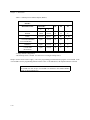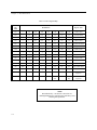
1
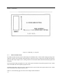
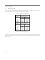
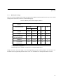
 XVME-103
3U RAM/ROM/Flash Memory Module
USER’S MANUAL
ACROMAG INCORPORATED
30765 South Wixom Road
P.O. BOX 437
Wixom, MI 48393-7037 U.S.A.
Tel: (248) 295-0885
Fax: (248) 624-9234
Email: [email protected]
Copyright 2012, Acromag, Inc., Printed in the USA.
Data and specifications are subject to change without notice.
8500-963B Xycom Revision Record
Revision
A
B
Description
Manual Released
Manual Updated (incorporated PCN #193)
Date
12/92
5/96
Trademark Information
Brand or product names are registered trademarks of their respective owners.
Copyright Information
This document is copyrighted by Xycom Incorporated (Xycom) and shall not be reproduced or copied
without expressed written authorization from Xycom.
The information contained within this document is subject to change without notice.
xycom
Technical Publication Department
750 North Maple Road
Saline, MI 48176-1292
313-429-4971
313-429-1010 (fax)
TABLE OF CONTENTS
CHAPTER
1
2
3
TITLE
PAGE
INTRODUCTION
1.1
Overview
1.2
Manual Structure
1.3
Module Operational Description
1.4
Specifications
1-1
1-2
1-3
1-4
INSTALLATION
2.1
Introduction
2.2
Location of Components Relevant to Installation
2.3
Jumper and Switch List
2.4
Jumper and Switch Descriptions
2.4.1
VME Address/Memory Chip Size
2.4.2
Memory Device Size
2.4.3
Address Modifier Decode
2.4.4
Memory Device Speed
2.4.5
Memory Device Type
2.4.6
SYSRESET* Driver
2.4.7
SYSFAIL* Driver
2.5
Installing Memory Chips on the XVME-103
2.6
Memory Backup Power
2.7
Securing the On-board Battery
2-1
2-1
2-2
2-3
2-3
2-4
2-6
2-8
2-9
2-12
2-12
2-13
2-15
2-16
REAL TIME CLOCK PROGRAMMING
3.1
Introduction
3.2
Real Time Clock/Readable Bank Information Port
3.3
Register Map
3.4
Register Descriptions
3.5
Programming Procedures
3-1
3-2
3-3
3-5
3-9
APPENDICES
A
B
C
VMEbus Connector/Pin Description
Quick Reference Guide
Block Diagram/Assembly Drawing/Schematics
2-i
Table of Contents
FIGURE
1-1
2-1
2-2
2-3
2-4
2-5
2-6
2-7
TABLE
1-1
1-2
2-1
2-2
2-3
2-4
2-5
2-6
2-7
2-8
ii
TITLE
PAGE
Operational Block Diagram
Location of Jumper, Switches, Sockets and Connectors
XVME-103 Memory Map
Addressing - 4 x Chip Size
EPROM Memory Chip Pinouts
SRAM Memory Chip Pinouts
FLASH/EEPROM Memory Chip Pinouts
Notched End of the Memory Chip
1-3
2-1
2-5
2-6
2-11
2-11
2-12
2-14
TITLE
PAGE
XVME-103 Memory Module Hardware Specifications
Memory Module Environmental Specifications
Switch and Jumper List
VME Base Address Select Bank 1 & 2
Memory Device Size (Bank 1 and Bank 2)
Address Modifier Switches
Memory Device Speed Switch
Memory Device Pinout Jumpers (Bank 1)
Memory Device Pinout Jumpers (Bank 2)
Jumper Configuration for each Option
1-4
1-5
2-2
2-3
2-4
2-7
2-8
2-9
2-10
2-15
Chapter 1 - INTRODUCTION
1.1 OVERVIEW
The XVME-103 RAM/ROM Memory Module is a single-high, VMEbus compatible board that can accommodate up
to 4 Mbytes of RAM, 8 Mbytes of EPROM, 4 Mbytes of FLASH or 4 Mbytes of EEPROM. The module is designed
with an on-board battery backup circuit to provide power to CMOS RAM devices in the event of a power failure.
The XVME-103 has eight 32-pin JEDEC sockets, which are divided into two separate memory banks, containing four
sites each. Each bank is designed to employ memory devices of the same type and speed, and each bank can be
independently configured (via jumpers and switches) in terms of:
•
•
•
•
•
•
VME Address
Address Modifier Decode
Memory Device Speed
Memory Device Type
Memory Device Size
Memory Backup Power Source
The XVME-103 RAM/ROM Memory Module has power down memory protection circuitry which prevents data from
being written to memory when the power supply voltage falls below 4.65 volts. The module also has the option of
asserting SYSRESET under this condition. Another option is to drive SYSFAIL when a low battery is detected on power
up.
The XVME-103 supports 8-bit and 16-bit data transfers, including read modify write (RMW) cycles.
Chapter 1 – Introduction
1.2 MANUAL STRUCTURE
The purpose of Chapter One is to introduce the general specifications and functional capabilities of the XVME-103.
Chapter Two will develop the various aspects of module installation and operation.
1-2
Chapter One
A general description of the memory module, including functional and environmental
specifications, and VMEbus compliance information.
Chapter Two
Information covering switch/jumper options, memory chip and cardcage installation
procedures.
Appendix A
Backplane signal/pin descriptions.
Appendix B
Quick reference guide of jumper and switch configurations, and memory device timing.
Appendix C
Block diagram, assembly drawing, and schematics.
XVME-103 RAM/ROM Memory Module
December 1992
1.3 MODULE OPERATIONAL DESCRIPTION
Figure 1-1 below shows an operational block diagram of the XVME-103 RAM/ROM Memory Module.
Figure 1-1. Operational Block Diagram
2-3
Chapter 1 – Introduction
1.4
SPECIFICATIONS
Table 1-1 lists the XVME-103 Memory Module's Hardware Specifications.
Table 1-1. XVME-103 Memory Module Hardware Specifications
Characteristic
Specification
Maximum Memory Capacity:
RAM
EPROM
FLASH
EEPROM
2 Banks of 4 sites
4 Mbytes Total
8 Mbytes Total
4 Mbytes Total
4 Mbytes Total
Device Sizes Supported:
RAM
EPROM
FLASH
EEPROM
128K by 8 up to 512K by 8
128K by 8 up to 1024K by 8
128K by 8 up to 512K by 8
128K by 8 up to 512K by 8
Device Speeds Supported:
50, 100, 150, 200 ns
Power Requirements:
+5 V @ .7A typ. .9 A max.
Battery Rating:
1.9 Amp hours
Battery Life:
3.0 years typ. (using a 628128 Hitachi RAM or equivalent
device)
VMEbus Compliance
Complies with VMEbus Specifications, IEEE 1014, Rev C.1
•
•
•
•
•
1-4
A24:D16/D08(EO)DTB Slave for memory banks
4 BUS GRANT INs are connected to their respective BUS GRANT OUTs
IACKIN is connected to IACKOUT
SINGLE - 3U Form Factor
Supports RMW
XVME-103 RAM/ROM Memory Module
December 1992
Table 1-2 lists the XVME-103 Memory Module's Environmental Specifications.
Table 1-2. Memory Module Environmental Specifications
Characteristic
Temperature:
Operating
Non-operating
Humidity:
Altitude:
Operating
Non-Operating
Vibration:
Operating
Non-operating
Shock:
Operating
Non-operating
Specification
0° to 65° C (32° to 149° F)
-40° to 85° C (-40° to 185° F)
5% to 95% RH non-condensing
(Extreme low humidity conditions may require special protection
against static discharge)
Sea level to 10,000 ft. (3048 m)
Sea level to 50,000 ft. (15240 m)
5 to 2000 Hz
.015" peak to peak
2.5 g peak acceleration
5 to 2000 Hz
.030" peak to peak
5.0 g peak acceleration
30 g peak acceleration,
11 msec duration
50 g peak acceleration,
11 msec duration
NOTE
To meet the shock and vibration specifications, you must secure the on-board battery
with the Ty-Wrap included with the XVME-103. Refer to Chapter 2 for information
on how to secure it.
2-5
Chapter 1 – Introduction
1-6
Chapter 2 - INSTALLATION
2.1 INTRODUCTION
This chapter explains how to configure the XVME-103 Memory Module before installing the module into a VMEbus
system. Information on jumper and switch options and locations is also included.
2.2 LOCATION OF COMPONENTS RELEVANT TO INSTALLATION
The jumpers, switches, memory sockets, and the VMEbus P1 connector on the XVME-103 Memory Module are
illustrated in Figure 2-1 below.
Figure 2-1. Location of Jumpers, Switches, Sockets and Connectors
Chapter 2 - Installation
2.3 JUMPER AND SWITCH LIST
Prior to installing the XVME-103 Memory Module, it is necessary to configure several switch and jumper options. Table
2-1 provides a list of all the switches and jumpers.
Table 2-1. Switch and Jumper List
Switch
SW1
SW2
Jumper
J1
J2
J3
J4
J5
J6
J7
J8
J9
J10
J11
J12
J13
J14
J15
J16
J17
J18
2-2
Description
Configuration Bank 1, SYSRESET
Configuration Bank 2, SYSFAIL
Description
VME Address A23 Bank 2
VME Address A22 Bank 2
VME Address A21 Bank 2
VME Address A20 Bank 2
VME Address A19 Bank 2
+5VSTBY, Alternate Power Source
VME Address A23 Bank 1
VME Address A22 Bank 1
VME Address A21 Bank 1
VME Address A20 Bank 1
VME Address A19 Bank 1
Battery, Alternate Power Source
VCC or VBU Bank 2
VCC or VBU Bank 1
Program FLASH Bank 1
Program FLASH Bank 2
Program FLASH Bank 1
Program FLASH Bank 2
XVME-103 RAM/ROM Memory Module
April 1996
2.4 JUMPER AND SWITCH DESCRIPTIONS
The two memory banks are independently configurable, via jumpers and switches, to define six different memory module
parameters:
•
•
•
•
•
•
VME Address
Address Modifier Decode
Memory Device Speed
Memory Device Size
Memory Device Type
Memory Backup Power Source
The following subsections examine these jumper and switch options in detail, showing specifically when and how
jumpers should be configured.
2.4.1
VME Address
Five jumpers exist for each bank (10 total) to define the VMEbus address. Table 2-2 lists the jumpers and their
definitions. The bank will occupy a VMEbus address space of four times the memory chip size. The bank must be
assigned to a boundary which is a multiple of four times the memory chip size.
Table 2-2. VME Base Address Select Bank 1 & 2
BANK 1
128K x 8
256K x 8
512K x 8
1024K x 8
Base Address Bit
=1
=0
=1
=0
=1
=0
=1
=0
A23(J7)
A
B
A
B
A
B
A
B
A22(J8)
A
B
A
B
A
B
A
B
A21(J9)
OUT
B
OUT
B
OUT
B
A
A
A20(J10)
OUT
B
OUT
B
A
A
A
A
A19(J11)
OUT
B
A
A
A
A
A
A
A23(J1)
A
B
A
B
A
B
A
B
A22(J2)
A
B
A
B
A
B
A
B
A21(J3)
OUT
B
OUT
B
OUT
B
A
A
A20(J4)
OUT
B
OUT
B
A
A
A
A
A19(J5)
OUT
B
A
A
A
A
A
A
BANK 2
2-3
Chapter 2 - Installation
2.4.2
Memory Device Size
The XVME-103 contains two switch settings per Bank that determine the device size. Table 2-3 shows the memory
device size for Banks 1 and 2.
Table 2-3. Memory Device Size (Bank 1 and Bank 2)
BANK 1
128K x 8 Devices
256K x 8 Devices
512K x 8 Devices
1024K x 8 Devices
BANK 2
128K x 8 Devices
256K x 8 Devices
512K x 8 Devices
1024K x 8 Devices
SWITCH 1 POSITION
1
2
Closed*
Closed
Open
Open
Closed*
Open
Closed
Open
SWITCH 2 POSITION
1
2
Closed*
Closed
Open
Open
Closed*
Open
Closed
Open
*XVME-103 factory default configuration
2-4
XVME-103 RAM/ROM Memory Module
April 1996
The following is an example of the jumpers and switch settings required to install 256Kx8 EPROMS in bank 1.
Example:
27020 256Kx8 EPROMs are to be installed in bank 1 with a VMEbus base address of 900000 Hex.
J7 A
J8 B
J9 B
J10 Out
J11 A
Switch 1 Position 1 Closed
Switch 1 Position 2 Open
Bank 1 will reside in memory address: 900000 Hex. through 9FFFFF Hex.
Figure 2-2 shows the memory map for the XVME-103 and Figure 2-3 (on the following page) shows the bank addressing
four times the memory chip size.
Figure 2-2. XVME-103 Memory Map
2-5
Chapter 2 - Installation
Figure 2-3. Addressing - 4 x Chip Size
2.4.3
Address Modifier Decode
The address modifier decode uses three switch settings for each bank (6 total). The first switch setting is privilege select.
When the switch is closed, the bank will respond only to supervisor accesses. When open, the bank will respond to
supervisor and non-privileged accesses. During each access of a bank, that bank's LED will momentarily light on the
front panel.
The second switch setting is program access select. When open, the module will respond to program accesses. When
closed, the module does not respond to program accesses.
The third switch setting is data access select. When this switch is open, the bank will respond to data accesses. When
closed, the bank does not respond to data accesses.
Table 2-4, on the following page, lists these switch settings and their definitions.
2-6
XVME-103 RAM/ROM Memory Module
April 1996
Table 2-4. Address Modifier Switches
BANK 1
SWITCH 1 POSITION
7 ClosedSupervisory only AM2=1
7 Open* Supervisory & non-privileged AM2=no preference
8 Open* Data Access - Responds to address modifier codes 3DH or 39H
8 ClosedNo Data Access - Will not respond to 3DH or 39H
9 Open* Program Access - Responds to address modifier codes 3EH or 3AH
9 ClosedNo program access - Will not respond to 3EH or 3AH
BANK 2
SWITCH 2 POSITION
7 ClosedSupervisory only AM2=1
7 Open* Supervisory & non-privileged AM2=no preference
8 Open* Data Access - Responds to address modifier codes 3DH or 39H
8 ClosedNo Data Access - Will not respond to 3DH or 39H
9 Open* Program Access - Responds to address modifier codes 3EH or 3AH
9 ClosedNo Program Access - Will not respond to 3EH or 3AH
*Factory default configuration
The two switch settings (8 & 9) are independent of one another. When both the data access select and program access
select switch positions are closed, the bank is disabled from VMEbus accesses.
2-7
Chapter 2 - Installation
2.4.4
Memory Device Speed
Two switch settings exist for each bank to define the speed of the memory devices. Selections are 50, 100, 150, and 200
ns access times. Table 2-5 lists the switches and speed definition for each device.
Table 2-5. Memory Device Speed Switch
BANK 1
50 ns
100 ns
150 ns
200 ns
BANK 2
50 ns
100 ns
150 ns
200 ns
SWITCH 1 POSITION
5
6
Closed
Closed
Open*
Open
Closed
Open
Closed*
Open
SWITCH 2 POSITION
5
6
Closed
Closed
Open*
Open
Closed
Open
Closed*
Open
*XVME-103 factory default configuration
VMEbus access timing is a function of the memory device speed of the bank being accessed. Data strobe asserted to
DTACK* asserted will typically be 100 ns plus the chosen access time. Data strobe negated to DTACK* negated will
typically be 40 ns.
2-8
XVME-103 RAM/ROM Memory Module
April 1996
2.4.5
Memory Device Type
There are two switch settings and five jumpers per Bank on the XVME-103 that determine the device type. These switch
settings are listed in Tables 2-6 and 2-7, on the following page.
Table 2-6. Memory Device Pinout Jumpers (Bank 1)
BANK 1
MEMORY TYPE
SWITCH 1
J15
J17
J14
3
4
EPROM
Closed
Closed
B
B
A
RAM*
Closed*
Open*
B*
B*
A*, B**
Open
Closed
B
B
A
EEPROM
Open
Closed
B
B
A
+12V FLASH
(Write/Read)
Open
Closed
A
A
A
+5V FLASH (WR/RD)
+12V FLASH (Read)
* Factory Default Configuration
**B if backup source is needed. See Section 2.6 to configure backup source.
Jumpers J15 and J17 are used to supply +12V to the programming pin VPP needed to program +12V FLASH. If +5V
FLASH is used or programming will not be done to the +12V FLASH device, the B position must be selected.
2-9
Chapter 2 - Installation
Table 2-7. Memory Device Pinout Jumpers (Bank 2)
BANK 2
MEMORY TYPE
SWITCH 2
J16
J18
J13
3
4
EPROM
Closed
Closed
B
B
A
RAM*
Closed*
Open*
B*
B*
A*, B**
Open
Closed
B
B
A
EEPROM
Open
Closed
B
B
A
+12V FLASH
(Write/Read)
Open
Closed
A
A
A
+5V FLASH (WR/RD)
+12V FLASH (RD)
* Factory Default Configuration
**B if backup source is needed. See Section 2.6 to configure backup source.
Jumpers J16 and J18 are used to supply +12V to the programming pin VPP needed to program +12V FLASH. If the
+5V FLASH is used or programming will not be done to the +12 FLASH device, the B position must be selected.
NOTE
The XVME-103 does accept +5V FLASH if it conforms to the standard JEDEC
pinout, as shown in Figure 2-6.
2-10
XVME-103 RAM/ROM Memory Module
April 1996
Figures 2-4 through 2-6 show the memory chip pinouts for EPROM, SRAM, and FLASH/EEPROM.
Figure 2-4. EPROM Memory Chip Pinouts
2-5. SRAM Memory Chip Pinouts
2-11
Chapter 2 - Installation
Figure 2-6. FLASH/EEPROM Memory Chip Pinouts
2.4.6
SYSRESET* Driver
A SYSRESET* driver is provided to assert SYSRESET* when the power monitor circuitry detects that Vcc is less than
4.65V. To enable the SYSRESET* driver, open switch 1, position 10. To disable the SYSRESET* driver, close switch
1 position 10. Default = switches closed.
2.4.7
SYSFAIL* Driver
A SYSFAIL* driver is provided to assert SYSFAIL* when a low battery is detected at power up. A low battery LED
on the front panel will also light. To enable the SYSFAIL* driver, open switch 2 position 10. To disable the SYSFAIL*
driver, close switch 2 position 10. Any access to either bank will deassert the SYSFAIL* driver once asserted. Default
= switches closed.
NOTE
If the SYSFAIL* signal is asserted by the XVME-103, it can be cleared by any access
to the board. The low battery LED will remain on even if the SYSFAIL* signal has
been deasserted by an access to the XVME-103.
2-12
XVME-103 RAM/ROM Memory Module
April 1996
2.5
INSTALLING MEMORY CHIPS ON THE XVME-103
As previously mentioned, there are a total of eight 32-pin sockets intended for use by RAM, EPROM, FLASH, and
EEPROM devices on the XVME-103 Module.
Installing memory in any of the sockets requires setting the proper jumpers and installing the memory devices. This
NOTE
Static precautions should be exercised when handling the memory chips, especially the
CMOS RAM chips.
procedure is detailed on the next page.
NOTE
Memory configuration jumpers should be set before installing memory devices.
2-13
Chapter 2 - Installation
•
With all power removed from the board, locate the proper socket. Refer to Figure 2-1 for the location of sockets
and banks.
•
Refer to the notched end of the memory chips as shown in Figure 2-7.
Figure 2-7. Notched End of the Memory Chip
•
Line up the pins on each chip with the socket holes found at the inside top of each socket location, and push each
chip firmly and evenly into place.
•
Check to make sure that the chips are fully seated in the bottom of the sockets, with no pins bent or out of alignment
in the sockets.
2-14
XVME-103 RAM/ROM Memory Module
April 1996
2.6
MEMORY BACKUP POWER
During power loss, CMOS RAM chips may have an alternative power source connected to retain the data stored. Two
alternative power sources are available: the on board battery or the +5V STDBY signal from the VMEbus. The
following chart shows the jumper configuration for each option.
Table 2-8. Jumper Configuration for each Option
Alternative
Power Source
J12
J6
None*
On-Board Battery
3.6V On +5V STDBY
+5V On +5V STDBY
A*
B
A
A
OUT*
OUT
B**
A**
*Factory default configuration
**If +5V STDBY voltage is equivalent to battery voltage of approximately 3.6V, select B. If +5V STDBY
voltage is equivalent to VCC voltage of approximately +5V, select A.
In order to achieve maximum battery life, RAM chips must have a small data retention current. Most static RAM
suppliers have chips that guarantee very low data retention currents. To calculate the typical battery life, use the
following equation:
Hours of battery life =
1,900,000
((n x IsB) + 22)
where:
IsB
=
the data retention current required by the particular RAM chips, in micro amperes
n
=
the number of RAM chips selected to be battery backed
Example:
Hitachi 628128LP-12 RAM chips have a typical IsB of 2uA:
Battery Life
=
1,900,000
((8 x 2) + 22)
=
50000 hours = 5.7 years
Each bank can be individually configured to either have or not have backup battery power, as shown by the jumper
settings below:
Bank 1
No backup power =
Backup power = J14B
J14A
No backup power =
J13A
Bank 2
2-15
Chapter 2 - Installation
Backup power = J13B
2-16
XVME-103 RAM/ROM Memory Module
April 1996
If backup power is not needed for either bank, J6 should be in the OUT position and J12 should be in the A position.
If EPROM, FLASH or EEPROM is installed in any bank, the Vcc jumper, (J14A for Bank 1 and J13A for Bank 2)
should be installed to prevent drawing current from the alternate power source.
2.7
SECURING THE ON-BOARD BATTERY
After the sockets have been populated, secure the on-board battery with the included Ty-Wrap. Follow the steps below
to install the Ty-Wrap (refer to Figure 2-1 to determine placement of the Ty-Wrap).
Insert the pointed end of the Ty-Wrap through the hole adjacent to the battery. The Ty-Wrap should be fed through
from the component side of the XVME-103.
Bring the pointed end of the Ty-Wrap up between the edge of the board and the front panel, slipping the pointed end
through the sqaure hole in the opposete end of the Ty-Wrap.
Continue to pull the pointed end through the square hold until the Ty-Wrap is tight against the battery. You can cut
the Ty-Wrap to remove the excess.
2-17
Chapter 3 - REAL TIME CLOCK PROGRAMMING
3.1
INTRODUCTION
This chapter focuses on programming the Real Time Clock (RTC). It gives a complete description of each of the RTC
registers, as well as procedures for programming the various functions of the RTC.
The following is a list of Acronyms and Abbreviations used in this chapter.
ACRONYM AND ABBREVIATION LIST
AIE
AF
CIE
CF
ENB
RTC
Alarm Interrupt Enable
Alarm Flag
Carry Interrupt Enable
Carry Flag
Enable
Real Time Clock
Chapter 3 – Real Time Clock
3.2
REAL TIME CLOCK/READABLE BANK INFORMATION PORT
All writes and reads to the Real Time Clock are at odd memory locations (D7-D0). The Real Time Clock uses 16 registers,
and the remaining odd memory locations in the 1K address space are shadowed on 32 byte blocks. Table 3-1, shows the
location of the registers.
The device type and size for the two banks are readable at even locations (D15-D8) in the same Short I/O address space as
the Real Time Clock. This is readable only and is shadowed 1K times. Table 3-1 shows register addressing and Table 3-2
shows data bit definitions.
Table 3-1. Register Addressing
Offset from 1K Base
Address
0
1
2
3
4
5
6
7
8
9
A
B
C
D
E
F
10
11
12
13
14
15
16
17
18
19
1A
1B
1C
1D
1E
1F
20
21
.
.
.
3-2
Real Time Clock/Configuration Register
Configuration Reg.
RTC Register 1
Configuration Reg.
RTC Register 3
Configuration Reg.
RTC Register 5
Configuration Reg.
RTC Register 7
Configuration Reg.
RTC Register 9
Configuration Reg.
RTC Register B
Configuration Reg.
RTC Register D
Configuration Reg.
RTC Register F
Configuration Reg.
RTC Register 11
Configuration Reg.
RTC Register 13
Configuration Reg.
RTC Register 15
Configuration Reg.
RTC Register 17
Configuration Reg.
RTC Register 19
Configuration Reg.
RTC Register 1B
Configuration Reg.
RTC Register 1D
Configuration Reg.
RTC Register 1F
Same as 00
Same as 01
.
.
.
XVME-103 RAM/ROM Memory Module
April 1996
Table 3-2. Data Bit Definitions
Bit
D15
D14
Memtypelb
Memtypela
D13
D12
Memsizelb
Memsizela
D11
D10
Memtype2b
Memtype2a
D9
D8
Memsize2b
Memsize2a
D7-D0
Real Time Clock Bits
3.3
Bit Location
Determines Memory Type Bank 1 (upper bit)
Determines Memory Type Bank 1 (lower bit) 00=EPROM 01=SRAM 10=FLASH/EEPROM
Determines Memory Size Bank 1 (upper bit)
Determines Memory Size Bank 1 (lower bit) 00=128K x 8 01=256K x 8 10=512K x 8 11=1024K
x8
Determines Memory Type Bank 2 (upper bit)
Determines Memory Type Bank 2 (lower bit) 00=EPROM 01=SRAM 10=FLASH/EEPROM
Determines Memory Size Bank 2 (upper bit)
Determines Memory Size Bank 2 (lower bit) 00=128K x 8 01=256K x 8 10=512K x 8 11=1024K
x8
REGISTER MAP
Table 3-3, on the following page, shows the address map of the 16 RTC registers. The registers are accessed on odd-byte
addresses, beginning at the base address of the XVME-103 in the VMEbus Short I/O space.
3-3
Chapter 3 – Real Time Clock
Table 3-3. RTC Register Map
RTC
Reg.
Offset
Bit Definitions
Register Name
01h
*
1 Hz
2 Hz
4 Hz
8 Hz
16 Hz
32 Hz
64 Hz
64 Hz Counter
03h
*
c-s40
c-s20
c-s10
c-s8
c-s4
c-s2
c-s1
Seconds Counter
05h
*
c-mi40
c-mi20
c-mi10
c-mi8
c-mi4
c-mi2
c-mi1
Minutes Counter
07h
*
*
c-h20
c-h10
c-h8
c-h4
c-h2
c-h1
Hours Counter
09h
*
*
*
*
*
c-w4
c-w2
c-w1
Day of Week Counter
0Bh
*
*
c-d20
c-d10
c-d8
c-d4
c-d2
c-d1
Day Counter
0Dh
*
*
*
c-mo10
c-mo8
c-mo4
c-mo2
c-mo1
Month Counter
0Fh
c-y80
c-y40
c-y20
c-y10
c-y8
c-y4
c-y2
c-y1
Year Counter
11h
ENB
1 Hz
2 Hz
4 Hz
8 Hz
16 Hz
32 Hz
64 Hz
64 Hz Alarm
13h
ENB
a-s40
a-s20
a-s10
a-s8
a-s4
a-s2
a-s1
Seconds Alarm
15h
ENB
a-mi40
a-mi20
a-mi10
a-mi8
a-mi4
a-mi2
a-mi1
Minutes Alarm
17h
ENB
*
a-h20
a-h10
a-h8
a-h4
a-h2
a-h1
Hours Alarm
19h
ENB
*
*
*
*
a-w4
a-w2
a-w1
Day of Week Alarm
1Bh
ENB
*
a-d20
a-d10
a-d8
a-d4
a-d2
a-d1
Day Alarm
1Dh
CF
*
*
CIE
AIE
*
*
AF
Control
Register A
1Fh
RAM7
RAM6
RAM5
RAM4
TEST
30 sec
ADJ
RESET
Start/
Stop
Control
Register B
NOTE
Bits indicated by '*' are unused. These bits are
unchanged during write operations and will always read
'0' during read operations.
3-4
XVME-103 RAM/ROM Memory Module
April 1996
3.4
REGISTER DESCRIPTIONS
The functions of the bits in the RTC registers are described in detail in the following sections.
3.4.1
64 Hz Counter (RTC Register 01h)
The 64 Hz Counter Register is a read-only register which can be used to gain access to time values with greater resolution
than one second. The bits in this register will toggle from '0' to '1' at the indicated frequency. For example, the 2 Hz bit
(bit 5) will change from '0' to '1' twice per second.
This register is clocked by an internal 128 Hz source. An internal "carry" occurs each time the 128 Hz clock rolls over,
indicating that the data in the 64 Hz Counter Register is changing. The length of the carry operation is 125 μs. If the
64 Hz Counter Register is being read during this time, the Carry Flag (CF) (bit 7 of Control Register A) will be set to
'1'. The data read during this time is not valid, so the register must be read again. Refer to the procedure for reading the
RTC time in section 3.4.3.
The 64 Hz Counter Register can only be reset using the RESET or 30-sec. ADJ operations. Refer to the description of
these bits in Control Register B in section 3.4.7.3
3.4.2
Seconds, Minutes, Hour Counter Registers (RTC Registers 03h, 05h, 07h)
These registers are used to set or read the RTC time of day using the 24-hour system. Each of the registers is encoded
in BCD format. For example, 59 seconds is expressed in the Seconds Counter Register as '01011001'.
Similar to the 64 Hz Counter Register, an internal carry will occur in the Seconds Counter Register once each second.
The length of the internal carry is 125 μs. If the Seconds Counter Register is being read during this time, the CF (bit
7 of Control Register A) will be set to '1'. The data read during this time is not valid, so the register must be read again.
Refer to the procedure for reading the RTC time in section 3.5.3
None of these registers is affected by RESET. The Seconds Counter and Minutes Counter registers are affected by the
30-sec. ADJ operation. Refer to the description of these bits in Control Register B in section 3.4.7.3
3-5
Chapter 3 – Real Time Clock
3.4.3
Day of Week Counter Register (RTC Register 09h)
The Day of Week Counter Register is used to set or read the day of the week. The day is encoded with a value from 0
to 6, according to the following chart.
3.4.4
Data
0
1
2
3
4
5
6
Day of Week
Sun.
Mon.
Tue.
Wed.
Thu.
Fri.
Sat.
Day, Month, and Year Counter Registers (RTC Registers 0Bh, 0Dh, 0Fh)
These registers are used to set or read the RTC calendar date. Each of these registers is encoded in BCD format. For
example, the 25th day of the month would be encoded in the Day Counter Register as '00100101'.
Only the last two digits of the year are used. Leap years are automatically recognized (Note: A year whose last two digits
are a multiple of four is recognized as a leap year).
3.4.5
64 Hz Alarm - Day Alarm Registers (RTC Registers 11h through 1Bh)
These registers are used to set the time at which the RTC triggers an alarm condition. Bit 7 of each of these registers
is the register's enable (ENB) bit. If an alarm register's ENB bit is set, the RTC uses that register in its comparison to
its corresponding counter register to determine if the alarm time has been reached. Two or more alarm registers may
be enabled at a time. When the values in the counter registers match the corresponding values in the enabled alarm
registers, the alarm condition is met. This can be thought of as a logical AND of the alarm registers that are enabled.
The RTC then sets the Alarm Flag (AF) bit in Control Register A. Since interrupts from the RTC are not used on the
XVME-103, the AF bit is the only indication to the host processor that the alarm time has been reached.
3.4.6
Control Register A (RTC Register 1Dh)
CF
*
*
CIE
AIE
*
*
AF
The only bits that are used in this register are the CF and the AF bits. Since interrupts from the RTC are not used on the
XVME-103, the Carry Interrupt Enable (CIE) and Alarm Interrupt Enable (AIE) bits are unused and should always be
written as '0'.
3-6
XVME-103 RAM/ROM Memory Module
April 1996
3.4.6.1 Carry Flag (CF)
The CF bit indicates that an internal carry has overlapped with a read from the 64 Hz Counter Register or a carry
occurred from the Seconds Counter Register. After each read operation, the CF bit should be polled to ensure that the
data read is valid. If the CF bit is set after a read operation, the data is not valid and must be read again. Refer to the
procedure for reading the RTC time in section 3.4.2
The CF bit can be reset by writing a '0' to it during any period except the carry period. A write of '1' to this bit is invalid.
3.4.6.2 Alarm Flag (AF)
The AF bit indicates to the host processor that the time specified in the enabled alarm registers has been reached. This
bit will remain set as long as the corresponding counter registers match the alarm registers. When the alarm condition
is no longer true, the AF bit will automatically be cleared to '0'.
The AF bit may be reset by writing a '0' to it during any period except the alarm period. In other words, writing a '0' to
the AF bit while the alarm condition is still true will reset the bit to '0' but only momentarily. The AF bit will be set again
immediately due to the alarm condition. A write of '1' to this bit is invalid.
3.4.7
Control Register B (RTC Register 1Fh)
RAM7
RAM6
RAM5
RAM4
TEST
ADJ
RESET
Start/Stop
NOTE
The TEST bit should always be set to '0'. User functions
are not guaranteed if the TEST bit has been set to '1'.
The bits in this register are used to control the operation of the RTC. It contains four defined bits which are used to test,
adjust, reset, start or stop the counter. The other four bits may be employed by the user as read-write bits to be used as
RAM or flag bits.
3-7
Chapter 3 – Real Time Clock
3.4.7.1 RAM
These bits may be used as RAM or as flag bits at the user's discretion. These are readable/writable bits which retain their
state upon power down. These bits may only be used if the TEST bit has been set to '0'.
3.4.7.2 TEST
This bit is used to test the RTC at the factory and should always be set to '0' by the user's program. Failure to do so will
result in improper operation of the RTC.
3.4.7.3 ADJ (30-Second Adjust)
This bit is used to execute the 30-second adjustment feature of the RTC, which can be used to automatically synchronize
the RTC to another clock source. When a '1' is written to this bit, the Minutes Counter Register will be adjusted
according to the value in the Seconds Counter Register. If the Seconds Counter Register value is less than 30, the
Minutes Counter Register is unchanged. Otherwise, a carry will occur in the Minutes Counter Register. The 64 Hz
Counter Register and the Seconds Counter Register are both reset to 00h.
After being written to '1', the ADJ bit will remain set for 250 μs while the 30-second adjust operation takes place. The
bit will then be reset to '0' automatically.
3.4.7.4 RESET
This bit is used to reset the 64 Hz Counter Register to 00h to initialize the dividing circuit. This operation is typically
done with the counter stopped in order to set the RTC time and date before restarting the RTC.
After being written to '1', the RESET bit will remain set for 250 μs while the reset operation takes place. The bit will
then be reset to '0' automatically.
3.4.7.5 Start/Stop
This bit is used to start and stop the RTC. When a '0' is written to this bit, the RTC stops counting. When a '1' is written
to this bit, counting begins (or continues).
3-8
XVME-103 RAM/ROM Memory Module
April 1996
3.5
PROGRAMMING PROCEDURES
This section describes the programming procedures required for the RTC. Included are procedures for initializing the
RTC, setting or reading the RTC, using the alarm function, and using the RTC as a long term timer.
3.5.1
Power-on Initialization
The RTC on the XVME-103 must be initialized after power is first applied to the device. Initialization is only required
when the power is initially turned on. As long as battery backup is enabled, the RTC will not need to be initialized after
the VMEbus system is powered up. Follow the procedure for initializing the RTC registers as indicated in the flow chart
and instructions below.
•••••••••••••••••••••••••••••
•
Power Applied
•When power is first applied, all registers are undefined.
•••••••••••••••••••••••••••••
•
•••••••••••••••••••••••••••••
•
TEST bit <-- 0
•
To ensure proper operation (write '0' every time).
•••••••••••••••••••••••••••••
•
•••••••••••••••••••••••••••••
•
Wait 3 Seconds
•
Time delay necessary for oscillator stabilization.
•••••••••••••••••••••••••••••
•
•••••••••••••••••••••••••••••
• Set the counter registers •
• and alarm registers, and •
• initialize the control
•
• registers, as desired.
•
•••••••••••••••••••••••••••••
•
•
NOTE
The RTC chip has no hardware means for resetting the
registers. Therefore, after power is first applied to the
device, all registers must be initialized.
3-9
Chapter 3 – Real Time Clock
Follow the procedure below to initialize the RTC after initial power is applied:
3.5.2
1.
The TEST bit (bit 3 of Control Register B) is undefined after initial power up. Therefore,
calendar/clock operation is also undefined. Set the TEST bit to '0' before continuing with
initialization.
2.
Delay for 3 seconds before continuing with initialization. This time is required for oscillator
stabilization within the RTC chip.
3.
Since interrupts from the RTC are not used on the XVME-103, clear the CIE (bit 4 of Control Register
A) and AIE (bit 3 of Control Register A) bits to '0'.
4.
The Start/Stop bit (bit 0 of Control Register B) is undefined at power-up. This bit should be cleared
to '0' to stop the clock in order for the time to be set.
Time Setting Procedure
There are two ways that the RTC time can be set. If the date and time are to be set from scratch, the clock should be
stopped. This is the easiest way for the RTC time to be set. Alternatively, RTC registers can be set while the clock is
running. Both methods are described in the following sections.
3-10
XVME-103 RAM/ROM Memory Module
April 1996
3.5.2.1 Setting the Time with the RTC Stopped
If all of the date and time registers need to be set, stopping the clock is the preferred method for initializing the RTC.
The procedure for setting the RTC time while it is stopped is described in the flow chart and instructions below.
•
•
•••••••••••••••••••••••••••••
•
Stop the Clock
•
•••••••••••••••••••••••••••••
•
•••••••••••••••••••••••••••••
•
Reset the Clock
•
•••••••••••••••••••••••••••••
•
•••••••••••••••••••••••••••••
•
Wait for Reset
•
•••••••••••••••••••••••••••••
•
•••••••••••••••••••••••••••••
• Set the counter registers •
• and alarm registers, as •
•
desired.
•
•••••••••••••••••••••••••••••
•
•••••••••••••••••••••••••••••
•
Start the Clock
•
•••••••••••••••••••••••••••••
•
Clear the Start/Stop bit in Control Register B.
Set the RESET bit in Control Register B.
Do not set the Counter Registers until RESET bit
returns to '0'.
Set the Start/Stop bit in Control Register B.
Follow the procedure below to set the RTC time with the clock stopped:
1.
Stop the RTC by clearing the Start/Stop bit (bit 0 of Control Register B) to '0'. The clock will then
be stopped, but no registers will be affected.
2.
Since the 64 Hz Counter Register is a read-only register, it must be reset with the RESET bit. Reset
the 64 Hz Counter Register by setting the RESET bit (bit 1 of Control Register B) to '1'.
3.
Wait for the reset operation to conclude by polling the RESET bit until it has been reset to '0'. The
RTC automatically clears the RESET bit when the reset operation is complete.
4.
Set the Seconds Counter through Year Counter Registers to the desired values. Except for the Day
of Week Counter Register, these registers are encoded in BCD format.
5.
Start the RTC by setting the Start/Stop bit (bit 0 of Control Register B) to '1'.
3-11
Chapter 3 – Real Time Clock
3.5.2.2 Setting Registers with the RTC Running
If only one or a few of the date and time registers need to be set, they can be set while the RTC is running. The algorithm
is more complicated, involving verification of the write operations by checking the CF. The procedure for setting the
RTC time while it is running is described in the flow chart and instructions below.
•
••••••••••••••••••••••
•
•••••••••••••••••••••••••••••
•
•
Clear CF
•
•
•••••••••••••••••••••••••••••
•
•
•
•••••••••••••••••••••••••••••
•
• Write to Counter Register •
•
•••••••••••••••••••••••••••••
•
•
•
•••••••••••••••••••••••••••••
• YES • Verify Write Operation
•
••••••••
(CF = 1 ?)
•
•••••••••••••••••••••••••••••
• NO
•
Clear the Carry Flag in Control Register A.
Poll CF bit in Control Register A.
(Repeat for each register to be set)
Follow the procedure below to set the RTC time with the clock running:
3-12
1.
Clear the CF bit in Control Register A to '0'. Note: To prevent the AF bit from being cleared as well,
set the AF bit to '1' for the write operation.
2.
Set the desired time or date register by writing to the appropriate counter register (RTC Registers 03h
to 0Fh).
3.
Poll the CF bit in Control Register A. If the CF bit is '0', the write operation was successful and the
time or date register has been set.
4.
If the CF bit is '1', a carry has occurred and the procedure must be repeated. The internal carry period
lasts for a maximum of 125 μs. Wait 125 μs before attempting the procedure again. Restart the
procedure by clearing the CF bit to '0' (Step 1).
XVME-103 RAM/ROM Memory Module
April 1996
3.5.3
Time Reading Procedure
The following flow chart and instructions demonstrate the procedure for reading the RTC time and date. Reading the
RTC time and date requires the use of the CF to validate the data read from the counter registers.
•
••••••••••••••••••••••
•
•••••••••••••••••••••••••••••
•
•
Clear CF
•
•
•••••••••••••••••••••••••••••
•
•
•
•••••••••••••••••••••••••••••
•
• Read the Counter Register •
•
•••••••••••••••••••••••••••••
•
•
•
•••••••••••••••••••••••••••••
• YES •
Verify Read Operation
•
••••••••
(CF = 1 ?)
•
•••••••••••••••••••••••••••••
• NO
•
Clear the Carry Flag in Control Register A.
Poll CF bit in Control Register A.
(Repeat for all counter registers)
Follow the procedure below to read the RTC time and date:
1.
Since interrupts are not used, there is no need to be concerned with handling an interrupt from a carry
operation. (The CIE and AIE bits in Control Register A should always be written with '0').
2.
Clear the CF bit in Control Register A to '0'. Note: To prevent the AF bit from being cleared as well,
set the AF bit to '1' for the write operation.
3.
Read the desired time or date register by reading from the appropriate counter register (RTC Registers
03h to 0Fh).
4.
Poll the CF bit in Control Register A. If the CF bit is '0', the read operation was successful and the time
or date register data is valid.
5.
If the CF bit is '1', a carry has occurred and the procedure must be repeated. The internal carry period
lasts for a maximum of 125 μs. Wait 125 μs before attempting the procedure again. Restart the
procedure by clearing the CF bit to '0' (Step 2).
3-13
Chapter 3 – Real Time Clock
3.5.4
RTC Alarm Function
The RTC alarm function can be used to determine when the RTC time has reached a specified time, without having to
read the entire set of RTC registers. The alarm time is specified by the user, and when the RTC time reaches the alarm
time, the AF is set. The alarm registers (64 Hz, Seconds, Minutes, Hours, Day of Week, and Day) each have an enable
(ENB) bit which controls whether that register is used in the comparison. Two or more alarm registers may be enabled
simultaneously.
The following flow chart and instructions demonstrate the procedure for setting up the RTC alarm function.
•
•
•••••••••••••••••••••••••••••
•
Clock Running ...
•
•••••••••••••••••••••••••••••
•
•••••••••••••••••••••••••••••
•
Set the alarm time and •
•
set appropriate ENB
•
• bits in alarm registers •
•••••••••••••••••••••••••••••
•
•••••••••••••••••••••••••••••
•
Clear AF
•
•••••••••••••••••••••••••••••
•
•••••••••••••••••••••••••••••
• Monitor the alarm time
•
•
(Check AF)
•
•••••••••••••••••••••••••••••
Enable only those alarm registers that are to be
used in the comparison.
Clear the Alarm Flag in Control Register A.
Follow the procedure below to setup and monitor the alarm function:
3-14
1.
Since interrupts are not used, there is no need to be concerned with handling an interrupt from a the
alarm function. (The AIE and CIE bits in Control Register A should always be written with '0').
2.
Determine which of the alarm registers needs to be used in the comparison. For those registers, set
the desired alarm time and set the ENB bit to '1'.
3.
Clear the AF bit in Control Register A to '0'. Note: To prevent the CF bit from being cleared as well,
set the CF bit to '1' for the write operation.
4.
Monitor the AF bit in Control Register A until it becomes set to '1'. When this occurs, the alarm time
has been reached. The AF bit will remain set as long as the RTC time matches the alarm time. The
AF bit can be cleared by writing a '0' to it, but will be set again immediately if the alarm condition is
still met. To avoid this, either set the alarm time to a different time, or clear all of the ENB bits of the
alarm registers.
XVME-103 RAM/ROM Memory Module
April 1996
3.5.5
Application as a Long Term Timer
The RTC can be used as a long-term timer and will keep accurate track of the year, month and day. If used in this
application, setting the correct date is required. The RTC will properly handle the number of days in each of the twelve
months, including leap years.
NOTE
A year whose lower two digits are divisible by four is
recognized as a leap year.
3-15
APPENDIX A - VMEBUS CONNECTOR/PIN DESCRIPTION
A.1
VMEBUS SIGNAL IDENTIFICATION
Table A-1 (on pages 1 through 5) shows the VMEbus Signal Identification. Table A-2, on page 6, shows the Backplane P1
pin assignments.
Table A-1. VMEbus Signal Identification
Signal
Mnemonic
Connector and
Pin Number
ACFAIL*
1B:3
IACKIN*
1A:21
IACKOUT*
1A:22
Signal Name and Description
AC FAILURE: Open-collector driven signal which indicates that the AC
input to the power supply is no longer being provided, or that the required
input voltage levels are not being met.
INTERRUPT ACKNOWLEDGE IN: Totem-pole driven signal.
IACKIN* and IACKOUT* signals form a daisy-chained acknowledge.
The IACKIN* signal indicates to the VME board that an acknowledge
cycle is in progress.
INTERRUPT ACKNOWLEDGE OUT: Totem-pole driven signal.
IACKIN* and IACKOUT* signals form a daisy-chained acknowledge.
The IACKOUT* signal indicates to the next board that an acknowledge
cycle is in progress.
ADDRESS MODIFIER (bits 0-5): Three-state driven lines that provide
additional information about the address bus, such as: size, cycle type,
and/or DTB master identification.
AM0-AM5
AS*
1A:23
1B:16, 17
18, 19
1C:14
ADDRESS STROBE: Three-state driven signal that indicates a valid
address is on the address bus.
1A:18
A-1
Appendix A - VMEbus Connector/Pin Description
Table A-1. VMEbus Signal Identification (Continued)
Signal
Mnemonic
Connector
and
Pin Number
Signal Name and Description
A01-A23
1A:24-30
1C:15-30
ADDRESS BUS (bits 1-23): Three-state driven address lines that specify a
memory address.
A24-A31
2B:4-11
ADDRESS BUS (bits 24-31): Three-state driven bus expansion address
lines.
BBSY*
1B:1
BUS BUSY: Open-collector driven signal generated by the current DTB
master to indicate that it is using the bus.
BCLR*
1B:2
BUS CLEAR: Totem-pole driven signal generated by the bus arbitrator to
request release by the DTB master if a higher level is requesting the bus.
BERR*
1C:11
BG0IN* BG2IN*
1B:4,6,
8,10
BG0OUT* BG3OUT*
A-2
1B:5,7,
9,11
BUS ERROR: Open-collector driven signal generated by a slave. It
indicates that an irrecoverable error has occurred and the bus cycle must be
aborted.
BUS GRANT (0-3) IN: Totem-pole driven signals generated by the Arbiter
or Requesters. Bus Grant In and Out signal indicates to this board that it may
become the next bus master.
BUS GRANT (0-3) OUT: Totem-pole driven signals generated by
Requesters. These signals indicate that a DTB master in the daisy-chain
requires access to the bus.
XVME-103 RAM/ROM Memory Module
December 1992
Table A-1. VMEbus Signal Identification (Continued)
Signal
Mnemonic
Connector
and
Pin Number
Signal Name and Description
BR0*-BR3*
1B:12-15
BUS REQUEST (0-3): Open-collector driven signals generated by
Requesters. These signals indicate that a DTB master in the daisy-chain
requires access to the bus.
DS0*
1A:13
DATA STROBE 0: Three-state driven signal that indicates during byte and
word transfers that a data transfer will occur on data bus lines (D00-D07).
DS1*
1A:12
DTACK*
1A:16
DATA STROBE 1: Three-state driven signal that indicates during byte and
word transfers that a data transfer will occur on data bus lines (D0-D15).
DATA TRANSFER ACKNOWLEDGE: Open-collector driven signal
generated by a DTB slave. The falling edge of this signal indicated that valid
data is available on the data bus during a read cycle, or that data has been
accepted from the data bus during a write cycle.
DATA BUS (bits 0-15): Three-state driven, bi-directional data lines that
provide a data path between the DTB master and slave.
D00-D15
1A:1-8
1C:1-8
GND
1A:9,11,
15,17,19,
1B:20,23
1C:9
2B:2,12,
22,31
GROUND
A-3
Appendix A - VMEbus Connector/Pin Description
Table A-1. VMEbus Signal Identification (Continued)
Signal
Mnemonic
IACK*
IRQ1*
IRQ7*
Connector
and
Pin Number
1A:20
1B:24-30
Signal Name and Description
INTERRUPT ACKNOWLEDGE: Open-collector or three-state driven
signal from any master processing an interrupt request. It is routed via
the backplane to slot 1, where it is looped-back to become slot 1
IACKIN* in order to start the interrupt acknowledge daisy-chain.
INTERRUPT REQUEST (1-7): Open-collector driven signals,
generated by an interrupter, which carry prioritized interrupt requests.
Level seven is the highest priority.
LONGWORD: Three-state driven signal indicates that the current
transfer is a 32-bit transfer.
LWORD*
1C:13
RESERVED: Signal line reserved for future VMEbus enhancements.
This line must not be used.
(RESERVED)
2B:3
A reserved signal which will be used as the clock for a serial
communication bus protocol which is still being finalized.
SERCLK
1B:21
A reserved signal which will be used as a transmission line for serial
communication bus messages.
SERDAT
1B:22
SYSCLK
1A:10
A-4
SYSTEM CLOCK: A constant 16-MHz clock signal that is
independent of processor speed or timing. It is used for general system
timing use.
XVME-103 RAM/ROM Memory Module
December 1992
Table A-1. VMEbus Signal Identification (Continued)
Signal
Mnemonic
Connector
and
Pin Number
Signal Name and Description
SYSFAIL*
1C:10
SYSTEM FAIL: Open-collector driven signal that indicates that a failure
has occurred in the system. It may be generated by any module on the
VMEbus.
SYSRESET*
1C:12
SYSTEM RESET: Open-collector driven signal which, when low, will
cause the system to be reset.
WRITE*
1A:14
WRITE: Three-state driven signal that specifies the data transfer cycle in
progress to be either read or written. A high level indicates a read operation,
a low level indicates a write operation.
+5V STDBY
1B:31
+5V
1A:32
1B:32
1C:32
2B:1,13,32
+12V
1C:31
-12V
1A:31
+5 VDC STANDBY: This line supplies +5 VDC to devices requiring
battery backup.
+5 VDC POWER: Used by system logic circuits.
+12 VDC POWER: Used by system logic circuits.
-12 VDC POWER: Used by system logic circuits.
A-5
Appendix A - VMEbus Connector/Pin Description
A.2
BACKPLANE CONNECTOR P1
The following table lists the P1 pin assignments by pin number order. (The connector consists of three rows of pins labeled
rows A, B, and C.)
Table A-2. P1 Pin Assignments
Pin
Number
1
2
3
4
5
6
7
8
9
10
11
12
13
14
15
16
17
18
19
20
21
22
23
24
25
26
27
28
29
30
31
32
A-6
Row A
Signal
Mnemonic
Row B
Signal
Mnemonic
Row C
Signal
Mnemonic
D00
D01
D02
D03
D04
D05
D06
D07
GND
SYSCLK
GND
DS1*
DS0*
WRITE*
GND
DTACK
GND
AS*
GND
IACK*
IACKIN*
IACKOUT*
AM4
A07
A06
A05
A04
A03
A02
A01
-12V
+5V
BBSY*
BCLR*
ACFAIL*
BG0IN*
BG0OUT*
BG1IN*
BG1OUT*
BG2IN*
BG2OUT*
BG3IN*
BG3OUT*
BR0*
BR1*
BR2*
BR3*
AM0
AM1
AM2
AM3
GND
SERCLK(1)
SERDAT(1)
GND
IRQ7*
IRQ6*
IRQ5*
IRQ4*
IRQ3*
IRQ2*
IRQ1*
+5V STDBY
+5V
D08
D09
D10
D11
D12
D13
D14
D15
GND
SYSFAIL*
BERR*
SYSRESET*
LWORD*
AM5
A23
A22
A21
A20
A19
A18
A17
A16
A15
A14
A13
A12
A11
A10
A09
A08
+12V
+5V
APPENDIX B - QUICK REFERENCE GUIDE
Tables B-1, B-2, B-3, and B-4 list the jumpers, switch bits, and their function.
Table B-1. Bank 1 Configuration Switches
Bank 1
Switch 1
Switch Position
Description
1=Open, 0=Closed
1
2
Bank 1 Memory Size (Upper Bit)
Bank 1 Memory Size (Lower Bit)
00=128K x 8
01=256K x 8
10=512K x 8
11=1024K x 8
3
4
Bank 1 Memory Type (Upper Bit)
Bank 1 Memory Select (Lower Bit)
00=EPROM
01=SRAM
10=FLASH/EEPROM
5
6
Bank 1 Speed Select (Upper Bit)
Bank 1 Speed Select (Lower Bit)
00=50 NS Access
01=100 NS Access
10=150 NS Access
11=200 NS Access
7
Bank 1 Supr/Nonpriv Select
8
Bank 1 Data Access
9
Bank 1 Program Access
0=Supr
1=Supr/Nonpriv
1=Respond to Prog. Acc
0=Don't Respond
1=Respond to Data Acc
0=Don't Respond
J14 is used to select VBU or VCC to the power pin (pin 32)
VCC = A pos
VBU = B pos
J15 and J17 are used to supply +12V to the programming pin VPP needed to program FLASH. If FLASH is not used or
programming will not be done to the device, select the A position.
+12V = B position
else = A position
B-1
Appendix B - Quick Reference Guide
Table B-2. VME Base Address Select Bank 1
BANK 1
128K x 8
256K x 8
512K x 8
1024K x 8
Base Address Bit
=1
=0
=1
=0
=1
=0
=1
=0
A23(J7)
A
B
A
B
A
B
A
B
A22(J8)
A
B
A
B
A
B
A
B
A21(J9)
OUT
B
OUT
B
OUT
B
A
A
A20(J10)
OUT
B
OUT
B
A
A
A
A
A19(J11)
OUT
B
A
A
A
A
A
A
B-2
XVME-103 RAM/ROM Memory Module
December 1992
Table B-3. Bank 2 Configuration Switches
Bank 2
Switch 2
Switch Position
Description
1=Open, 0=Closed
1
2
Bank 2 Memory Size (Upper Bit)
Bank 2 Memory Size (Lower Bit)
00=128K x 8
01=256K x 8
10=512K x 8
11=1024K x 8
3
4
Bank 2 Memory Type (Upper Bit)
Bank 2 Memory Type (Lower Bit)
00=EPROM
01=SRAM
10=FLASH/EEPROM
5
6
Bank 2 Speed Select (Upper Bit)
Bank 2 Speed Select (Lower Bit)
00=50 NS Access
01=100 NS Access
10=150 NS Access
11=200 NS Access
7
Bank 2 Supr/Nonpriv Select
8
Bank 2 Data Access
9
Bank 2 Program Access
0=Supr
1=Supr/Nonpriv
1=Respond to Prog. Acc
0=Don't Respond
1=Respond to Data Acc
0=Don't Respond
J13 is used to select VBU or VCC to the power pin (pin 32)
VBU = A pos
VCC = B pos
J16 and J18 are used to supply +12V to the programming pin VPP needed for +12V FLASH to program. If FLASH is
not used or programming will not be done to device, select the A position.
+12V = B position
else = A position
B-3
Appendix B - Quick Reference Guide
Table B-4. VME Base Address Select Bank 2
BANK 2
128K x 8
256K x 8
512K x 8
1024K x 8
Base Address Bit
=1
=0
=1
=0
=1
=0
=1
=0
A23(J1)
A
B
A
B
A
B
A
B
A22(J2)
A
B
A
B
A
B
A
B
A21(J3)
OUT
B
OUT
B
OUT
B
A
A
A20(J4)
OUT
B
OUT
B
A
A
A
A
A19(J5)
OUT
B
A
A
A
A
A
A
B-4
XVME-103 RAM/ROM Memory Module
December 1992
Table B-5 shows the jumper configuration for battery backup options.
Table B-5. Jumper Configuration
Alternative
Power Supply
J12
J6
None*
Battery
3.6V On +5V Standby
+5V On +5V Standby
A*
B
A
A
OUT*
OUT
B
A
*Factory shipped configuraton
Table B-6. Device Parameters For Memory Sites Banks 1 and 2
RAM Device
Parameter
Must be
Chosen Access Times
502NS
1003NS
1504NS
2005NS
tCO
<
50
100
150
200
tAA
<
79.5
129.5
179.5
235.5
tOE
<
65.5
115.5
165.5
229.5
tOLZ
>
0
0
0
0
tOHZ
<
47.5
47.5
47.5
47.5
tRC
<
50
100
150
200
tAS
<
16
16
16
16
tAW
<
74
124
174
224
tCW
<
45
95
145
195
tWP
<
60
110
160
210
tWR
<
12.5
12.5
12.5
12.5
tDH
<
9.5
9.5
9.5
9.5
tDW
<
50.5
100.5
150.5
200.5
tWC
<
50
100
150
200
B-5
Appendix B - Quick Reference Guide
1
A write occurs during the overlap of a low CS1 and a low WE. A write begins at the latest transition among
CS1 going low, and WE going low. A write ends at the earliest transition among CS1 going high, and WE
going high. Twp is measured from the beginning of write to the end of write.
2
Tas is measured from the address valid at the beginning of write.
3
Twr is measured from the earliest of CS1 or WE going high to the end of the write cycle.
4
During this period, I/O pins are in output state; therefore, the input signals of the opposite phase to the
outputs must not be applied.
Figure B-1. Write Timing Waveform
B-6
XVME-103 RAM/ROM Memory Module
December 1992
Figure B-2. Read Timing Waveform
B-7
APPENCIX C - BLOCK DIAGRAM/ASSEMBLY DRAWING/SCHEMATICS
Figure C-1. XVME-113 Block Diagram
C-1
Appendix C - Block Diagram/Assembly Drawing/Schematics
Figure C-2. Assembly Drawing
C-2