1
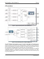
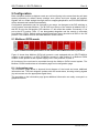
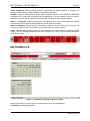
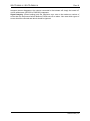
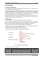
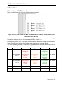
SDI-TD-MUX-4 / SDI-TD-DMUX-4 4 x SD-SDI / DVB-ASI over HD-SDI Time Division Multiplexer / De-Multiplexer User manual Rev. N Nevion Nordre Kullerød 1 3241 Sandefjord Norway Tel: +47 33 48 99 99 nevion.com SDI-TD-MUX-4 / SDI-TD-DMUX-4 Rev. N Nevion Support Nevion Europe Nevion USA P.O. Box 1020 3204 Sandefjord, Norway Support phone 1: +47 33 48 99 97 Support phone 2: +47 90 60 99 99 1600 Emerson Avenue Oxnard, CA 93033, USA Toll free North America: (866) 515-0811 Outside North America: +1 (805) 247-8560 E-mail: [email protected] See http://www.nevion.com/support/ for service hours for customer support globally. Revision history Current revision of this document is the uppermost in the table below. Rev. Repl. Date Sign N 12 2015-05-14 MB 12 11 2012-04-04 TB 11 10 2011-04-15 TB 10 - 2011-01-31 TB Change description Cover page update; DoC removed; no other changes to content Clarified the ASI data rate in the specification lists (updated chapters 1, 2 and 3). Corrected error in the description of the DIPs for fallback to internal video generator. Based on version 5.4 of MUX and DMUX codes and combined from earlier FLP3 versions of the manual. nevion.com | 2 SDI-TD-MUX-4 / SDI-TD-DMUX-4 Rev. N Contents 1 The SDI-TD-MUX-4 and SDI-TD-DMUX-4 at a glance ............................................ 4 1.1 Product versions .............................................................................................................. 4 2 Multiplexer specifications ......................................................................................... 5 3 De-multiplexer specifications ................................................................................... 6 4 Description............................................................................................................... 7 5 Configuration ........................................................................................................... 9 5.1 Multicon GYDA mode ...................................................................................................... 9 5.2 MUX DIP switches ..........................................................................................................16 5.3 DMUX DIP switches .......................................................................................................17 6 Connections........................................................................................................... 18 6.1 Power connections .........................................................................................................18 6.2 Backplane ......................................................................................................................18 6.3 The main board ..............................................................................................................19 7 Operation ............................................................................................................... 21 7.1 Front panel LED indicators .............................................................................................21 7.2 GPI alarms .....................................................................................................................22 7.3 RS422 commands ..........................................................................................................22 8 Laser safety precautions........................................................................................ 27 General environmental requirements for Nevion equipment..................................... 28 Product Warranty ...................................................................................................... 29 Appendix A Materials declaration and recycling information..................................... 30 nevion.com | 3 SDI-TD-MUX-4 / SDI-TD-DMUX-4 Rev. N 1 The SDI-TD-MUX-4 and SDI-TD-DMUX-4 at a glance The SDI-TD-MUX-4 is a Flashlink time-division multiplexer (TDM) that allows any combination of four SD-SDI or DVB-ASI inputs to be transported over a single HD-SDI link according to the SMPTE 346M-2000 standard. The SDI-TD-DMUX-4 is a Flashlink time division de-multiplexer that recovers the four SDSDI or DVB-ASI input signals from the SMPTE 346M-2000 compliant transport signal. The key features of the combination SDI-TD-MUX-4 / SDI-TD-DMUX-4 include: Accepts any synchronous or asynchronous SD-SDI 270 Mbps input format as well as 270 Mbps DVB-ASI. Automatic input format detection for each channel. Mix of input formats allowed and correct format recovered at the de-multiplexer side. Built-in routing switcher at both ends. Separate stream clock reference data for each channel is transferred for remote clock regeneration. The four streams embedded in the HD-SDI are completely independent, no contamination of remaining streams when one or more inputs are lost. High performance optics for short and long haul applications available, including CWDM laser option. Optical and electrical 1.485 Gbps HD output TDM available simultaneously. Change-over functionality between de-multiplexer electrical and optical inputs. The transport signal is compliant with the SMPTE-346M-2000 standard, allowing use of a standard HD infrastructure for transport and switching of the multiplexed signal. EDH handling for the SD-SDI signals. Multicon interface allows remote control, status monitoring, error reporting and SNMP support. 1.1 Product versions SDI-TD-MUX-4 4xSD-SDI/DVB-ASI multiplexer with electrical HD-SDI output. SDI-TD-MUX-4-T 4xSD-SDI/DVB-ASI multiplexer with simultaneous electrical and optical HD-SDI outputs.1 SDI-TD-DMUX-4 HD-SDI to 4xSD-SDI/DVB-ASI de-multiplexer with electrical input. SDI-TD-DMUX-4-R HD-SDI to 4xSD-SDI/DVB-ASI de-multiplexer with both electrical and high sensitivity 9/125µm single mode optical input. 1 Several wavelength/power options exist. From a control perspective all these versions are identical, but the laser control block reports its parameters to the system controller. nevion.com | 4 SDI-TD-MUX-4 / SDI-TD-DMUX-4 Rev. N 2 Multiplexer specifications Electrical input Number of inputs Data rates Equalization Impedance Return loss Connector 4 independent SD-SDI, DVB-ASI or SDTI 270 Mbps, any DVB-ASI payload data rate2 Automatic up to 300m 75 ohm >15dB @ 270MHz BNC Electrical output (standard) Output signal Data rate Impedance Return loss Jitter (UI = Unit Interval) Peak to peak signal level Signal polarity Connector HD-SDI with TDM payload according to SMPTE 346M-2000 1485 Mbps 75 ohm >15dB @ 1485MHz Max. 0.2UI 0.8V ±0.1V Non-inverting BNC Optical output (optional) Output signal Transmission circuit fiber Light source Optical power Optical center wavelength Max. wavelength drift Jitter (UI = Unit Interval) Connector return loss Connector HD-SDI, TDM payload according to SMPTE 346M-2000 Single Mode F-P / DFB laser -7.5dBM @ 1310nm (F-P laser), 0 dBm (DFB laser) 1310nm, 1550nm, CWDM according to ITU-T G.694.2 ±20nm (F-P lasers), ±6nm (DFB lasers) Max. 0.2UI @ 1485Mbps better than 40dB w/ SM fiber SC/UPC Electrical Temperature range Power consumption Control 0 to +45 °C +5V/3.5 W, +15V/1.0W (4.5W when running on a single +5V supply) RS-422, Multicon GYDA enabled, SNMP Latency Electrical and optical delay Less than 100 us (combined through MUX and DEMUX) In addition comes 5 us/km of fiber signal propagation time Supported standards for electrical and optical ports SMPTE DVB-ASI 2 SMPTE 346M-2000, SMPTE 292M, SMPTE 259M, SMPTE 305.2M, SMPTE 297M, SMPTE RP165 EN50083-9 Early versions of the MUX/DMUX modules were limited to DVB-ASI payload data rates ≤ 35 Mbps. nevion.com | 5 SDI-TD-MUX-4 / SDI-TD-DMUX-4 Rev. N 3 De-multiplexer specifications Optical input Input signal Sensitivity Max multi mode fiber length Detector overload threshold Detector damage threshold Optical wavelength Transmission circuit fiber Connector return loss Connector HD-SDI, TDM payload according to SMPTE 346M-2000 Better than -25dBm 300m (version SDI-TD-DMUX-4-RM) Min. -6dBm > +1dBm 1200 - 1620nm Single Mode 9/125µm or multimode 50/125µm better than 40dB w/ SM fiber SC/UPC Electrical input Output signal Data rate Equalization Impedance Return loss Signal level Connector HD-SDI with TDM payload according to SMPTE 346M2000 1485 Mbps Automatic up to 100m 75 ohm >15dB @ 270MHz Nom. 800mV BNC Electrical output Number of outputs Data rates Impedance Return loss Jitter (UI = Unit Interval) Peak to peak signal level Signal polarity Connector 4 independent SD-SDI, DVB-ASI or SDTI 270 Mbps (see footnote on the previous page) 75 ohm >15dB @ 270MHz Max. 0.2UI 0.8V ±0.1V Non-inverting BNC Electrical Temperature range Power consumption Control 0 to +45 °C +5V/3.5 W, +15V /1.8W (5.2W when running on a single +5V supply) RS-422, Multicon GYDA enabled, SNMP Latency Electrical and optical delay Less than 100μs (combined through MUX and DEMUX) In addition comes 5us/km of fiber signal propagation time Supported standards for electrical and optical ports SMPTE DVB-ASI SMPTE 346M-2000, SMPTE 292M, SMPTE 259M, SMPTE 305.2M, SMPTE 297M, SMPTE RP165 EN50083-9 nevion.com | 6 SDI-TD-MUX-4 / SDI-TD-DMUX-4 Rev. N 4 Description Figure 1: Logical building blocks for SDI-TD-MUX-4(-T) Figure 2: Logical building blocks for SDI-TD-DMUX-4(-R) The SDI-TD-MUX-4 board transfers any or all of the four 270 Mbps input signals via an optical or electrical HD interface according to SMPTE 346M-2000. An SDI-TD-DMUX-4 board is required to reconstruct the four 270 Mbps signals, normally at a remote location and linked via an optical fiber or an electrical coax cable. The inputs to the SDI-TD-MUX-4 can be any combination of 270 Mbps SD-SDI or DVB-ASI (188 or 204 word packets). The output from the SDI-TD-MUX-4 module is either electrical HD according to the SMPTE 346M-2000 standard, or simultaneous electrical and optical HD according to the same standard if an optional laser module is purchased (in which case the module will identify itself as an SDI-TD-MUX-4-T). nevion.com | 7 SDI-TD-MUX-4 / SDI-TD-DMUX-4 Rev. N The SDI-TD-DMUX-4 board receives any combination of four 270 Mbps time division multiplexed SD-SDI or DVB-ASI signals embedded in the 1.485 Mbps HD signal according to SMPTE 346M-2000. If the customer has purchased an optional pin diode module for optical input (in which case the module will identify itself as an SDI-TD-DMUX-4-R), there will be an option available to select either input manually, or to select between them automatically. All outputs can be either 270 Mbps SD-SDI or DVB-ASI (188 or 204 word packets). Channel swapping (“shuffler”) is available either from DIP-switches or remotely via the standard Multicon GYDA interface. Shuffling is available in both modules, in case the two modules are on different control networks, or only one of the modules is even connected to the control network. I cases where fewer than four SD signal are transported, the shuffling feature can also be used to duplicate channels on the outputs, potentially saving a distribution amplifier. The SD-SDI clocks for each recovered SD channel will be regenerated based on a frequently received SCR counter (Stream Clock Reference – refer to the SMPTE 346M-2000 standard). This ensures a stable, low-jitter output. There are four signal generators available on the board. Each can be set to color bar 525, color bar 625, black 525 or black 625 from Multicon GYDA. Since the SDI-TD-DMUX-4 does not have a local clock reference input, a valid SD signal must be present in the HD stream from the SDI-TD-MUX-4 (i.e. at least one SD signal must be connected to one of the SDI-TDMUX-4 SD inputs) in order to guarantee that the output signals from the test signal generators in the SDI-TD-DMUX-4 are compliant with the SD clock requirements. The module will still generate an output based on the video signal that was lost, but without a clock reference there’s no guarantee that equipment down the signal chain will be able to lock (or remain locked) to that output. By default, there is no fallback for missing SD streams. If fallback is set to black or color bar, the video format (SD-SDI, 525 vs. 625 lines) will be selected automatically based on the signal that was lost. If the lost signal was DVB-ASI, no fallback will be available, regardless of the setting. The board measures the RSSI (Received Signal Strength Indicator) from the optical input. Normally, the readout (in the Multicon GYDA GUI) shows the signal strength within ±1-2 dB. However, the measurement is NOT calibrated and the readout should be used as an indication only. Also, while the readout is fairly linear within a range from -15 dBm to -30 dBm, outside this range the meter will just “bottom out” at -15dBm or -30dBm. If that occurs, disregard the actual readout but know that the signal is either strong enough with good margins or too weak to be detectable. nevion.com | 8 SDI-TD-MUX-4 / SDI-TD-DMUX-4 Rev. N 5 Configuration Both multiplexer and de-multiplexer cards are self-configuring in the sense that they will start working according to default factory settings once power and input signals are applied. Signals will be routed straight through without swapping/duplication and SD-SDI/DVB-ASI will be detected and handled automatically. Configuration parameters can be changed in two ways, via changes to the DIP switches or via the system controller Multicon. The 8th DIP from the top of the module is labeled OVR. If this DIP is set to the ON position, DIP switches 1-7 will control the module. Conversely, if it is set to the OFF position, DIPs 1-7 are disregarded altogether and the module is controlled from Multicon GYDA. Default settings as delivered from factory should be all DIPs in the Off position. The module will then be under Multicon GYDA control. 5.1 Multicon GYDA mode Figure 3: Multicon GYDA presentation of rack with an SDI-TD-MUX-4 module in position 2 Figure 3 shows how Multicon GYDA will present a rack equipped with an SDI-TD-MUX-4 module in rack position 2, an SDI-TD-DMUX-4 module in rack position 6, a Multicon GYDA module in rack position 9 and a power supply unit in rack positions 10 and 11. All functions of the card can be controlled through the Multicon GYDA control system. The Multicon GYDA interface has an information page and a configuration page. 5.1.1 Information page The information page shows a dynamic block diagram of the board and some additional information text. The block diagram updates with the board status, showing missing signals (by red crosses over the appropriate signal lines). The text table on the information page gives additional information not easily conveyed in a graphical manner. nevion.com | 9 SDI-TD-MUX-4 / SDI-TD-DMUX-4 Rev. N Figure 4: The MUX info page in Multicon GYDA. From the text table, we can read the following: All four cable equalizers are enabled (“Normal”), as opposed to “Bypassed”. Of the four reclockers, only reclocker 1 has been able to lock to an input signal. That reclockers 2-4 are unlocked can also be seen from the three red crosses in the block representation. The locked input is indicated as 270Mbps SD-SDI. The error counter has found no errors for input 1 (at least not errors of the types that should be counted), but plenty of errors for inputs 2-4. We can also tell that the voltages are reasonably close to their nominal values. And last, since this is a board with the laser option, we can see that the laser is powered and what kind of laser it is (wavelength, power and type). nevion.com | 10 SDI-TD-MUX-4 / SDI-TD-DMUX-4 Rev. N Figure 5: The DMUX info page in Multicon GYDA. From the text table, we can read the following: The electrical input has been manually selected. This (and the name of the module) also indicates that this board has the optional optical input installed. No carrier is detected on the optical input. Of the four streams, only stream 4 can be locked to and recovered. The locked stream is indicated to contain an 270Mbps SD-SDI. The line that says “Routing” is a list of how the streams are routed to the outputs. In this case we can see that output 1 is routed from stream 4, output 2 from stream 3 and so on. If fallback had been selected for the missing streams, “Stream3”, “Stream 2” and “Stream 1“ would have been replaced with the texts “Black” or “Cbar”. The error counter has found no errors for the HD input (at least not errors of the types that should be counted). We can also see that the voltages are reasonably close to their nominal values (It is quite normal for the 5V supply to be 0.2V – 0.3V under its nominal value). nevion.com | 11 SDI-TD-MUX-4 / SDI-TD-DMUX-4 Rev. N 5.1.2 Configuration page Figure 6: The MUX config page in Multicon GYDA. Starting from the top of the page, the following things can be set/adjusted: Card label: This field enables the user to set a name for each module (Actually, it’s the slot in the frame, as the label will persist even if the card/backplane combination is replaced by a completely different module.) The name will show up above the card type on the info page and on the conf page, and it will also be shown as a mouse-over text when the mouse cursor is held over the card’s icon in the pictured rack. Locate card: Flashes the 4 LEDs on the front of the module at about 0.5Hz for the number of seconds the user specifies. Firmware upgrade: The firmware for the onboard microcontroller and the FPGA can both be upgraded, if needed. This line only shows up if the Multicon GYDA system controller has found a folder containing Flashlink firmware files. Contact Nevion support if you need an updated firmware. nevion.com | 12 SDI-TD-MUX-4 / SDI-TD-DMUX-4 Rev. N Cable equalizers: (Stored setting) ‘Normal’ means that the cable equalizer is enabled. ‘Eq bypass’ means that the cable equalizer is bypassed (disabled). Shuffler: (Stored setting) this is where each transport stream (in the SMPTE 346M-2000 compatible HD video) has a physical input assigned to it. In this particular case a reversediagonal is formed; all four inputs are transported, but they have all changed places. Input 1…4 integrity: (Stored setting) sets the maximum error rate or the maximum number of errors that can be present before Multicon GYDA sets off an alarm. Input 1-4 integrity: (Stored setting) This setting is common for all the four error counters and sets which types of errors should be counted and which should be ignored. Laser: (Stored setting) this control is only available for boards with the optional optical output. The only setting available for the laser is power On or Off. All other settings should be done at the factory. Figure 7: The DMUX config page in Multicon GYDA. Starting from the top of the page, the following things can be set/adjusted: Card label: See MUX description. nevion.com | 13 SDI-TD-MUX-4 / SDI-TD-DMUX-4 Rev. N Locate card: See MUX description. Firmware upgrade: See MUX description. Input selector: (Stored setting). This control is only available for boards with the optional optical input. Here the user can select to force the input to be taken from either the electrical or the optical input, or allow the card to automatically select between them. In “Auto (pri opt)”, the operation is like this: 1. If there is a carrier on the optical input, this input will always be preferred. 2. If there is no carrier on the optical input, the electrical input will only be selected if it has got a carrier. 3. There is no check for signal lock and there are no significant delays before swapping to the other input. In “Auto (latch)” mode, the operation is like this: 1. On power-on, the board will start with selecting the optical input as default. 2. If, at any time, the lock is lost on the presently selected input, after a ~one second delay, the board will first check if there is a carrier on the other input. If it isn’t, the input select will remain unchanged. If there is a carrier on the other input, the board will swap to that input and try to lock to it. 3. If both inputs have a carrier, but the board is incapable of locking to any of the signals, the board will toggle between the two inputs until a lockable signal is applied to either of the two inputs. Then, this input will be selected. The toggling rate is about once per second while searching for a lockable signal. 4. If none of the inputs has a carrier, the board will remain at its present input selection (the last one it successfully locked to or tried to lock to). 5. If there is a carrier on only one of the inputs, only this input will be selected as long as this is the case (no toggling). 6. There will always be a one second delay before giving up the presently selected signal on loss of lock. 7. There will be no non-volatile memory for keeping the last selected input when in auto mode. The above algorithm will always start working to find a signal when starting the board. This means that, after power-on, the optical input will always win if there is a lockable signal present at that input. Shuffler: (Stored setting) Each SD output is here assigned to one of the transport streams (in the SMPTE 346M-2000 compatible HD video) or to one of the onboard generators. Note that in this particular case a reverse-diagonal is formed, and when combined with the reverse-diagonal we saw in the MUX, this means that input 1 on the MUX side is routed out as output 1 on the DMUX side, input 2 is routed out as output 2, and so forth. The option also exists to force one or more of the outputs to internal generators. This is primarily useful during site installation, to validate parts of the signal chain. Fallback (for SD-SDI only): If/when the SD-SDI is lost on the MUX side, or if the HD link between the MUX and the DMUX breaks down, the DMUX has optional fallback to internal generators. The video format (525 vs. 625 lines) will then be determined by the last valid video to be seen by that particular output, while the user selects the video pattern (black picture or color bars). If no fallback is selected, the output driver will simply be turned off when the card can no longer output a valid SD signal. This is also the behavior when transporting DVB-ASI: Since the card has no onboard DVB-ASI generators, and thus no valid fallback for DVB-ASI, the fallback logic will always treat a DVB-ASI gone missing as if the fallback option for that particular output was “None”. In other words, when a DVB-ASI nevion.com | 14 SDI-TD-MUX-4 / SDI-TD-DMUX-4 Rev. N transport stream disappears, the outputs connected to that stream will simply be turned off, until a valid stream (SD-SDI or DVB-ASI) reappears. Signal integrity: (Stored setting) sets the maximum error rate or the maximum number of errors that can be present before Multicon GYDA sets off an alarm. Also sets which types of errors should be counted and which should be ignored. nevion.com | 15 SDI-TD-MUX-4 / SDI-TD-DMUX-4 Rev. N 5.2 MUX DIP switches Switch # 1-3 Function name Shuffler Function DIPs Input to stream allocation: RD0 RD1 RD2 S1 S2 S3 S4 [OFF][OFF][OFF]: 1 2 3 4 [ON ][OFF][OFF]: 1 1 3 4 [OFF][ON ][OFF]: 1 1 3 3 [ON ][ON ][OFF]: 1 1 1 4 [ ---- ][ ---- ][ON ]: 1 1 1 1 4-6 ( ---- means “Don’t care”. As long as RD2=ON, any combination of values for RD0 and RD1 will give the same result.) EQ0 EQ1 EQ2 [OFF][OFF][OFF]: Bypassed: none [ON ][OFF][OFF]: Bypassed: 1 [OFF][ON ][OFF]: Bypassed: 1+2 [ON ][ON ][OFF]: Bypassed: 1+2+3 [ ---- ][ ---- ][ON ]: Bypassed: all Cable equalizer bypass ( ---- means “Don’t care”. As long as EQ2=ON, any combination of values for EQ0 and EQ1 will give the same result.) 7 8 --OVR --Off: Multicon GYDA mode On: Manual mode Comment Changing the shuffler DIPs to something other than [OFF][OFF][OFF] will substitute one or more of the inputs 24 for a duplicate of input 1 or 3. Usually this should rather be done on the DMUX side. Changing the cable equalizer DIPs to something other than [OFF][OFF][OFF] will bypass one or more of the cable equalizers. This will normally result in reduced performance. Only use this feature if you understand why you would want to do it. Reserved This DIP is only read at power up. OVR is short term for Multicon GYDA override. Table 1: MUX DIP switch functions (Upper left corner of board) OFF ON RD0 RD1 RD2 EQ0 EQ1 EQ2 --OVR 1 2 3 4 5 6 7 8 Switch 1 (’off’ / 0) Switch 2 (’off’ / 0) Switch 3 (’off’ / 0) Switch 4 (’off’ / 0) Switch 5 (’on’ / 1) Switch 6 (’off’ / 0) Switch 7 (’on’ / 1) Switch 8 (’on’ / 1) Remote Distribution Shown: 1=>1 , 2=>2 , 3=>3 , 4=>4 Cable Equalisers Shown: 1 and 2 bypass, 3 and 4 enabled Spare (not in use). Override. Shown: DIP switch control only Figure 8: MUX DIP switch settings exemplified nevion.com | 16 SDI-TD-MUX-4 / SDI-TD-DMUX-4 Rev. N 5.3 DMUX DIP switches Switch # 1-3 Function name Shuffler Function DIPs Stream to output allocation: 1 2 3 O1 O2 O3 O4 [OFF][OFF][OFF]: 1 2 3 4 [ON ][OFF][OFF]: 1 1 3 4 [OFF][ON ][OFF]: 1 1 3 3 [ON ][ON ][OFF]: 1 1 1 4 [ ---- ][ ---- ][ON ]: 1 1 1 1 ( ---- means “Don’t care”. As long as RD2=ON, any combination of values for RD0 and RD1 will give the same result.) 4 5 INPUT [OFF][OFF]: Optical (manually) [ON ][OFF]: Electrical (manually) [OFF][ON ]: Auto (pri. optical) [ON ][ON ]: Auto (latching) 4-5 Input selector 6-7 Video fallback 6 7 Output video [OFF][OFF]: Black, auto vstd. [ON][OFF ]: Color bar, auto vstd. [OFF ][ON]: No fallback [ON ][ON ]: No fallback (auto vstd. = automatic standard detection - 525/625 lines according to the lost SD-SDI signal) 8 OVR Off: Multicon GYDA mode On: Manual mode Comment Changing the shuffler DIPs to something other than [OFF][OFF][OFF] will substitute one or more of the inputs 24 for a duplicate of input 1 or 3. This means that the card can be used as a distribution amplifier. For boards without the optional optical input, electrical input will always be selected and these DIPs have no function. There is no on-board DVB-ASI signal generator available. When losing a DVBASI signal, no fallback is available. The output will simply be lost, regardless of the fallback setting. This DIP is only read at power up. OVR is short term for Multicon GYDA override. Table 2: DMUX DIP switch functions (Upper left corner of board) OFF ON 1 2 3 4 5 6 7 8 Switch 1 (’off’ / 0) Switch 2 (’off’ / 0) Switch 3 (’off’ / 0) Switch 4 (’off’ / 0) Switch 5 (’off’ / 0) Switch 6 (’off’ / 0) Switch 7 (’off’ / 0) Switch 8 (’off’ / 0) Routing Shown: 1=>1 , 2=>2 , 3=>3 , 4=>4 Input Select Shown: Auto, priority optical Output Select (when no input) Shown: black picture, auto video standard Mode. Shown: GYDA control enabled Figure 9: DMUX DIP switches exemplified nevion.com | 17 SDI-TD-MUX-4 / SDI-TD-DMUX-4 Rev. N 6 Connections 6.1 Power connections Power is applied to the board via the backplane board, which in turn is plugged into the power distribution bus in the Flashlink rack. The SDI-TD-MUX-4 board consumes slightly more than the full maximum of 3 watts from the +5V supply and slightly more than the full maximum of 1.5 watts from the +15V supply available at the backplane. The SDI-TD-DMUX-4 consumes 3.5W from the +5V supply and 1.8W from the +15V supply. In both cases this limits the number of boards in a rack to 8 boards plus Multicon GYDA, when using a standard single power supply. Note that both boards can run on a single 5V supply, but then the full power of about 4.5 watts will be drawn from the 5V supply. The boards automatically adapts to sharing the load between +5V and +15V when 15V is available. 6.2 Backplane The SDI-TD-MUX-4 and SDI-TD-DMUX-4 boards use the same backplane. Figure 10 shows the backplane rear view. The signal directions indicated are for the SDI-TDMUX-4 card, with the DMUX in parentheses. When the backplane is used for the SDI-TDDMUX-4, the directions of SD1-SD4, HD electrical and HD optical will be reversed. The SD1 to SD4 connectors are for 270 Mbps SD-SDI or DVB-ASI signals. The HD output carries the electrical HD-signal with the four input signals time division multiplexed according to the SMPTE 346M-2000 standard. The optical and electrical outputs both carry the same HD-signal. The GPI outputs are alarm signals for driving external alarm devices. SD2 Input HD Optical Output SD3 Input SD1 Input SD4 Input GPI Outputs HD Electrical Output Figure 10: Rear view of the backplane The following connectors are available: Name SD1 SD2 SD3 SD4 Description Input (Output) for 270 Mbps SD-SDI or DVB-ASI. Input (Output) for 270 Mbps SD-SDI or DVB-ASI. Input (Output) for 270 Mbps SD-SDI or DVB-ASI. Input (Output) for 270 Mbps SD-SDI or DVB-ASI. Connector Type BNC BNC BNC BNC nevion.com | 18 SDI-TD-MUX-4 / SDI-TD-DMUX-4 HD OPT GPI Rev. N Output (Input) for 1.485 Gbps HD-SDI (Multiplexed according to SMPTE 346M-2000). Optical output (input) for 1.485 Gbps HD-SDI. General Purpose Interface (transistor drivers for external alarm devices). BNC SC/UPC RJ-45 Unused inputs should be terminated to avoid alarms triggered by noise. 6.2.1 GPI/ Data connections RJ45 Figure 11: RJ45 Connector for GPI Signals The below table show the signals available on the GPI connector on the backplane. RJ45 Pin Number 8 7 6 5 4 3 2 1 Description GND Not Used Not Used Not Used GPI2 GPI3 GPI0 GPI1 6.3 The main board There are also a number of connectors on the board itself. None of these are intended for the end-user. For proper operation, make sure there is a jumper in the lower position of the connector located behind the DIP-switches (see Figure 12 and Figure 13 below). The rear end of the boards (with the connector that mates to the backplane) is towards the right side of the board. The boards must be mounted in a Flashlink FR-2RU-10-2 frame with dedicated backplanes. Avoid inserting the SDI-TD-MUX-4 or SDI-TD-DMUX-4 board into a wrong backplane, as this may cause electrical and/or mechanical damage to the main boards and/or the backplanes. nevion.com | 19 SDI-TD-MUX-4 / SDI-TD-DMUX-4 DIP switches OFF ON ’0’ ’1’ Jumper needed for proper operation LED indicators Rev. N Optical backplane connector Electrical backplane connector with signals and power lines Figure 12: MUX main board overview DIP switches OFF ON ’0’ ’1’ LED indicators Jumper needed for proper operation Optical backplane connector Electrical backplane connector with signals and power lines Figure 13: DMUX main board overview nevion.com | 20 SDI-TD-MUX-4 / SDI-TD-DMUX-4 Rev. N 7 Operation 7.1 Front panel LED indicators Figure 14 shows how the LEDs are located on the front panel. Figure 14: Front panel view for the MUX. The DMUX LEDs are identical, except that the lower LED refers to the HD input. The table below shows how the front panel LEDs are to be interpreted. The four LEDs correspond closely to the four GPI alarms explained in chapter 7.2. Note that the term “in error” in the table means that there is either a missing signal (no carrier detect) AND/OR the reclocker has not been able to lock to the incoming signal. The term “operating normally” means that a signal has been detected (carrier detect on the cable equalizer) AND the reclocker has been able to lock to the signal. Diode 1 Description Card status Red LED Power on, FPGA not configured Both SD inputs/streams (1 and 2) In error 2 Status of SD inputs/streams 1 and 2 3 4 (MUX) 4 (DMUX) Orange LED Not applicable One of the inputs/streams (1 or 2) in error Status of SD inputs/streams 3 and 4 Both SD inputs/streams (3 and 4) in error One of the inputs/streams (3 or 4) in error Status of HD OUT Status of HD IN Output failure Laser failure Input failure N/A Green LED Power on and FPGA configured Both inputs/streams (1 and 2) operating normally Both inputs/streams (3 and 4) operating normally Output OK and laser working Input OK No light No power to board No power to board No power to board No power to board No power to board nevion.com | 21 SDI-TD-MUX-4 / SDI-TD-DMUX-4 Rev. N 7.2 GPI alarms Four alarms are present on the RJ45 connector. These four GPI signals indicate the same status as the LEDs (see above): GPI0: On => Power on, FPGA not configured Off => Power on, FPGA configured GPI1: On => One of the channels (1 or 2) in error Off => Both channels (1 and 2) are OK GPI2: On => One of the channels (3 or 4) in error Off => Both channels (3 and 4) are OK GPI3: On => For SDI-TD-MUX-4: Laser failure, for SDI-TD-DMUX-4: No HD input Off => For SDI-TD-MUX-4: Laser OK, for SDI-TD-DMUX-4: Locked to an HD electrical or optical input signal.3 An active alarm condition means that the transistor is conducting. 7.3 RS422 commands 7.3.1 FLP4.0 required commands Block Blk # Commands Example Response Control - - ? ? product name\ SW rev n.m\ FW rev r.s\ protocol ver 4.0\ Hello command. Note 1: No other commands will be available until the card has received this hello. Note 2: This command will also enable checksums. Note 3: Cards are designed to be hot-swappable. To sync with the start of a new command, the cards will wait for a <lf> character before looking for a valid command. conf 0 - conf 0 *too long to list* Configuration settings Retrieves the card's configurable settings. Each addressable block is represented by a single line. Dynamic status may be included in response, but is usually reported in info only. - - info info *too long to list* Dynamic status info Blocks with static settings only will usually not be included, see conf above. - - chk off chk off ok Checksum off If issued twice in succession, this command will disable checksums. Note: Responses will still have the checksums appended. NOTE1:? command turns the checksum on again - - locate on <seconds> locate on 3 ok Card locator This command will cause all the 3 When optical input is selected by Multicon GYDA, alarm status is indicated only for optical input. When electrical input is selected from Multicon GYDA, status is indicated only for electrical input. When Multicon GYDA control is disabled or auto-select is chosen from Multicon GYDA, an alarm will be indicated only when both input HD signals are lost. nevion.com | 22 SDI-TD-MUX-4 / SDI-TD-DMUX-4 Block Blk # Commands Rev. N Example locate off locate off Response Control LEDs to flash for a user specified number of seconds. If omitted, the value <seconds> will be set to a default of 120 seconds. The flashing can be terminated at any time with locate off. - - address Address address <address> Card address This command will force the module to check and update its current rack and slot address. This is normally only done at start-up. - - filename filename tdmux103.ffw <name>'.'<extensio Firmware update n> The <name> part must match the card's hardware and include a revision number, and the extension must be either 'ffw' for FPGA firmware or 'mfw' for microcontroller firmware. After running this command, the board will be ready to receive its new firmware in Intel-hex format. filename tddmx321.ffw - - fin Fin ok Finalize Finalize the programming of the microcontroller. See description of the uC boot loader (separate document). misc 0 - STATUS NOT AVAILABLE BY SEPARATE COMMAND, ONLY FOUND in conf 0 AND info RESPONSES! prog | fin Misc info prog if the card is freshly programmed by the boot loader and the program is still un-finalized. fin is the normal condition. ovr if DIP-switch 16 is set to the ON position and the card is under DIPswitch control. Note 1: The info part of misc has additional functionality when locate is used: locating <remaining seconds>. This enables a visible countdown clock in Multicon GYDA, but is not a required part of FLP4. ' ' | ovr ' ' | err nevion.com | 23 SDI-TD-MUX-4 / SDI-TD-DMUX-4 Rev. N 7.3.2 Normal control blocks Block ceq Blk # Commands 0-3 (0) Example(s) ceq 0 Response Control cd | ncd Cable equalizer No control; only used to report carrier detected or no carrier detected. The DMUX has only one (ceq 0) for its HD electrical input, the MUX has one for each SD input, 4 in total. ceq 3 gpi 0 act inact gpi 0 inact act | inact Free-running vs. Locked to SD (MUX only) This gpi control is normally hidden to the end user. See the ‘cal’ command under ch. 7.3.3. ‘act’ means that the frequency of the HD output from the MUX is locked to one of the SD inputs, while ‘inact’ means that it is free-running. By locking to incoming SD, frequency drift is eliminated, but glitches will occur in all 4 outputs on the DMUX side if/when the MUX board must change its reference to a different SD input. lsr 0 on | off lambda <wavelen> lpwr <laser_pwr> type ( c | t | n ) lsr 0 off lsr 0 lambda 1310 lsr 0 lpwr 0 lsr 0 type c on type C 1310nm 0dBm Laser control (MUX only) Only on/off is directly available from Multicon. The other commands does not affect the laser itself, they just provide a tool to set information about the laser fitted to the board. C=CWDM T=DWDM N=None mtx 0 <input> <output> mtx 0 0 2 size 4:4 <in1> <in2> <in3> <in4> Input/stream shuffler mtx 0 controls which input is routed to which stream (MUX) or which stream is routed to each output (DMUX). mtx 1 <input> <output> mtx 0 0 2 size 4:1 <in1> Input selector (DMUX) 0: Always optical input 1: Always electrical input 2: Auto (pri optical) 3: Auto (latching) mtx 2 <input> <output> mtx 3 - size 2:1 <in1> Currently selected input (DMUX) 0: optical input 1: electrical input mtx 4 - size 6:4 < in1> <in2> <in3> <in4> Output status (DMUX) Reports the current status of all four outputs: 0: stream 1 1: stream 2 2: stream 3 3: stream 4 4: color bar 5: black Note that per SW 5.3, the fallbacks are not yet implemented and used. pin (0) - cd | ncd Pin diode status (DMUX only) No control. Only used to report Fallback generators (DMUX) Do not use, not fully implemented per SW 5.3. pin 0 nevion.com | 24 SDI-TD-MUX-4 / SDI-TD-DMUX-4 Block Blk # Commands Rev. N Example(s) Response Control carrier detected or no carrier detected. <nom>Vnom <volt>V Power supply monitors pwr 0 = 5.0V pwr 1 = 3.3V pwr 2 = 2.5V pwr 3 = 1.8V pwr 4 = 1.2V rcl 0 lock | lol Reclocker No commands available, only used to report lock status. The MUX board has one rcl block for each SD input, while the DMUX board has one rcl block for the HD input (rcl 0) and one rcl block for each recovered stream (rcl 1 – rcl 4). 0-3 reset vmon 3 reset vmon N cnt <errors> edh <edh_bits> err <error_bits> Video monitor (MUX) The vmon blocks 0-3 consist of an error counter for each SD input. Each error counter can be reset with the reset command. vmon 4 msk <bit_mask> vmon 4 msk 1 vmon 4 msk <bit_mask> Video monitor (MUX) Which errors are to be counted is set for all 4 error counters at once with the msk command. See the chapter on Signal integrity for explanation on the bit values. vmon 0 reset msk <bit_msk> reset msk 0x7b vmon 0 msk <bit_mask> vmon 0 cnt <errors> edh <edh_bits> err <error_bits> Video monitor (DMUX) The DMUX has one vmon block to monitor the incoming HD signal. See the chapter on Signal integrity for explanation on the bit values. pwr 0-5 - rcl 0-3 (4) vmon 7.3.3 Commands intended for debug/lab use only Block Commands example Response Control cal gpi sesame cal gpi sesame ok Toggles the visibility of normally hidden control blocks. rdp <page_number> rdp 4 *too long to list* Will list the contents of one page of the flash memory holding the FPGA program. rdr <address> rdr 0x0679 r<bits> <value> Ex: r16 0x0001 Reads a register value. Register value is returned as a hexadecimal numbers, and it’s preceded by either r8 or r16 to show if the rgister is 8 bit or 16 bit. MUX addresses: 0100-01FF: Deserializer 1 0200-02FF: Deserializer 2 0300-03FF: Deserializer 3 0400-04FF: Deserializer 4 0600-06FF: FPGA 0700-07FF: MCU EEPROM 0800-08FF: Serializer 0900-09FF: LED 1000-10FF: FPGA program flash nevion.com | 25 SDI-TD-MUX-4 / SDI-TD-DMUX-4 Block Commands Rev. N example Response Control DMUX addresses: 0100-01FF: Serializer 1 0200-02FF: Serializer 2 0300-03FF: Serializer 3 0400-04FF: Serializer 4 0600-06FF: FPGA 0700-07FF: MCU EEPROM 0800-08FF: Deserializer 0900-09FF: LED 1000-10FF: FPGA program flash rst <number> rst 1 wrr <address> <value> wrr 0x0679 1 ok <number>=0: Restarts all chips except MCU and FPGA. <number>=1: (DMUX only) Restarts deserializer <number>=2: Restarts MCU, thereby reinitializing entire board. <number>=4: Restarts FPGA only ok Write to register. See description of the ‘rdr’ command for valid address ranges. Note that the LEDs are read-only; all other registers are writable, even if the written value in some cases will be overwritten almost immediately. nevion.com | 26 SDI-TD-MUX-4 / SDI-TD-DMUX-4 Rev. N 8 Laser safety precautions These are guidelines to limit hazards from laser exposure. All the available EO (including ETH100) units in the Flashlink range include a laser. Therefore this note on laser safety should be read thoroughly. The lasers emit light at wavelengths from 1270 nm up to 1610 nm. This means that the human eye cannot see the beam, and the blink reflex cannot protect the eye. (The human eye can see light between 400 nm to 700 nm). A laser beam can be harmful to the human eye (depending on laser power and exposure time). Therefore: Be careful when connecting / disconnecting fiber pigtails (ends). Never look directly into the pigtail of the laser/fiber. Never use microscopes, magnifying glasses or eye loupes to look into a fiber end. Use laser safety goggles blocking light at 1310 nm and at 1550 nm Instruments exist to verify light output power: Power meters, IR-cards etc. Flashlink features: All the laser module cards in the Flashlink product range, are Class 1 laser products according to IEC 825-1 1993, and class I according to 21 CFR 1040.10 when used in normal operation. Maximum output power4: 5 mW Operating wavelengths: > 1270 nm 4 Max power is for safety analysis only and does not represent device performance. nevion.com | 27 SDI-TD-MUX-4 / SDI-TD-DMUX-4 Rev. N General environmental requirements for Nevion equipment 1. 2. - The equipment will meet the guaranteed performance specification under the following environmental conditions: Operating room temperature range: 0°C to 45°C Operating relative humidity range: <90% (non-condensing) The equipment will operate without damage under the following environmental conditions: Temperature range: -10°C to 55°C Relative humidity range: <95% (non-condensing) nevion.com | 28 SDI-TD-MUX-4 / SDI-TD-DMUX-4 Rev. N Product Warranty The warranty terms and conditions for the product(s) covered by this manual follow the General Sales Conditions by Nevion, which are available on the company web site: www.nevion.com nevion.com | 29 SDI-TD-MUX-4 / SDI-TD-DMUX-4 Rev. N Appendix A Materials declaration and recycling information A.1 Materials declaration For product sold into China after 1st March 2007, we comply with the “Administrative Measure on the Control of Pollution by Electronic Information Products”. In the first stage of this legislation, content of six hazardous materials has to be declared. The table below shows the required information. Toxic or hazardous substances and elements 組成名稱 Part Name SDI-TD-DMUX-4(-R) SDI-TD-MUX-4(-T) 鉛 汞 镉 六价铬 多溴联苯 多溴二苯醚 Lead Mercury Cadmium Hexavalent Polybrominated Polybrominated (Pb) (Hg) (Cd) Chromium biphenyls diphenyl ethers (Cr(VI)) (PBB) (PBDE) O O O O O O O: Indicates that this toxic or hazardous substance contained in all of the homogeneous materials for this part is below the limit requirement in SJ/T11363-2006. X: Indicates that this toxic or hazardous substance contained in at least one of the homogeneous materials used for this part is above the limit requirement in SJ/T11363-2006. This is indicated by the product marking: A.2 Recycling information Nevion provides assistance to customers and recyclers through our web site http://www.nevion.com/. Please contact Nevion’s Customer Support for assistance with recycling if this site does not show the information you require. Where it is not possible to return the product to Nevion or its agents for recycling, the following general information may be of assistance: Before attempting disassembly, ensure the product is completely disconnected from power and signal connections. All major parts are marked or labeled to show their material content. Depending on the date of manufacture, this product may contain lead in solder. Some circuit boards may contain battery-backed memory devices. nevion.com | 30