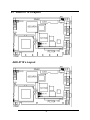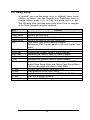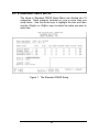
1
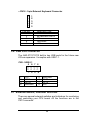
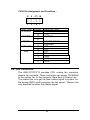
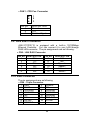
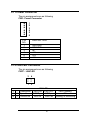
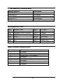
JUKI – 3711P/3712 Pentium® III, Celeron™, VIA Cyrix® III with Ethernet, VGA/LCD Ver 1.x @Copyright 2000 All Rights Reserved. Manual first edition March 7, 2000 The information in this document is subject to change without prior notice in order to improve reliability, design and function and does not represent a commitment on the part of the manufacturer. In no event will the manufacturer be liable for direct, indirect, special, incidental, or consequential damages arising out of the use or inability to use the product or documentation, even if advised of the possibility of such damages. This document contains proprietary information protected by copyright. All rights are reserved. No part of this manual may be reproduced by any mechanical, electronic, or other means in any form without prior written permission of the manufacturer. Trademarks JUKI-3711P/3712 is registered trademarks of ICP Electronics Inc., IBM PC is a registered trademark of International Business Machines Corporation. Intel is a registered trademark of Intel Corporation. AWARD is registered trademarks of AWARD SOFTWARE INTERNATION, INC. Other product names mentioned herein are used for identification purposes only and may be trademarks and/or registered trademarks of their respective companies. I Contents Introduction............................................................... 1 1.1 Specifications .....................................................................2 1.2 What You Have ..................................................................3 Installation ................................................................ 4 2.1 JUKI-3711P's/JUKI-3712's Layout......................................5 2.2 CompactFlash Disk Master/Slave Mode..............................6 2.3 Clear CMOS Setup .............................................................6 2.4 Inverter Power Select..........................................................6 2.5 LCD Panel Shift Clock/Panel VCC Select ...........................7 2.6 Serial Port B(COM2) Mode select .......................................7 2.7 Serial Port B -- RI or External Power Select ........................8 2.8 CPU Fan Power Voltage Select ..........................................8 Connection ............................................................... 9 3.1 Floppy Disk Drive Connector...............................................9 3.2 PCI IDE Disk Drive Connector .......................................... 10 3.3 Parallel Port ...................................................................... 11 3.4 Serial Ports ....................................................................... 11 3.5 Keyboard Connector ......................................................... 13 3.6 USB Port Connector.......................................................... 14 3.7 External Switch, Indicator and IrDA................................... 14 II 3.8 Fan Connector .................................................................. 15 3.9 LAN RJ45 Connector ........................................................ 16 3.10 VGA Connector................................................................. 16 3.11 Power Connector .............................................................. 17 3.12 LAN LED Connector.......................................................... 17 3.13 LCD Connector ................................................................. 18 3.14 Power LED Connector....................................................... 19 BIOS Setup ............................................................ 20 4.1 Introduction....................................................................... 20 4.2 Starting Setup ................................................................... 20 4.3 Using Setup ...................................................................... 21 4.4 Main Menu........................................................................ 22 Setup Items ..................................................................... 23 4.5 STANDARD CMOS SETUP.............................................. 25 4.6 BIOS FEATURES SETUP ................................................ 27 4.7 CHIPSET FEATURES SETUP.......................................... 32 4.8 INTEGRATED PERIPHERALS ......................................... 34 4.9 POWER MANAGEMENT SETUP ..................................... 37 4.10 PNP/PCI CONFIGURATION SETUP ................................ 40 4.11 Defaults Menu................................................................... 42 4.12 IDE HDD auto detection.................................................... 43 4.13 Supervisor/User Password Setting .................................... 43 4.14 Exit Selecting.................................................................... 44 III Appendix A. Watch-Dog Timer............................... 45 Appendix B. E2 Key™ Function................................ 47 Appendix C. Address Mapping............................... 48 IO Address Map ......................................................................... 48 st 1 MB Memory Address Map ..................................................... 49 IRQ Mapping Table .................................................................... 49 DMA Channel Assignments ........................................................ 49 IV 1 Introduction Welcome to the JUKI-3711P/3712 Pentium® III, Celeron Single Board Computer. The JUKI-3711P/3712 board is a PCISA/ISA form factor board, which comes equipped with high performance Pentium® III, Celeron™ , VIA Cyrix®III Processor and advanced high performance multi-mode I/O, designed for the system manufacturers, integrators, or VARs that want to provide all the performance, reliability, and quality at a reasonable price. In addition, the JUKI-3711P/3712 provides C&T MI69K VGA chip . The VGA which provides up to 1280x1024 resolution. The VGA memory is share main memory. An advanced high performance super AT I/O chip – Winbond W83977TF-AW is used in the JUKI-3711P/3712 board. Both onchip UARTs are compatible with the NS16C550. The parallel port and IDE interface are compatible with IBM PC/AT architecture's. JUKI-3711P/3712 uses Intel 82559ER Fast Ethernet Multifunction PCI Controller as LAN controller. The 82559ER is a fully integrated 10BASE-T/100BASE-TX LAN solution with high performance networking functions and low power features. JUKI-3711P/3712 uses the advanced VIA Chipset, 82C693A/82C596B. 1 1.1 Specifications : • CPU: Celeron™ 300- 566Mhz or above Processor Pentium® III (FC-PGA) 450 - 866Mhz or above Processor VIA Cyrix® III 466Mhz or above Processor • FSB: 66/100/133MHz • Bus: PCISA Bus, compatible to Jump PISA Ver. 1.07 (JUKI-3711P) ISA Bus (JUKI-3712) • DMA channels : 7 • Interrupt levels : 15 • Chipset : VIA 82C693A/82C596B • RAM memory : Single 168-pin DIMM sockets support SDRAM module. The max memory is up to 256MB. • Ultra ATA66 IDE Interface : Two PCI Enhance IDE hard drives. The south bridge supports Ultra ATA66 IDE interface. • Floppy disk drive interface : Single 2.88 MB, 1.44MB, 1.2MB, 720KB, or 360KB floppy disk drive. • Two high speed Serial ports : NS16C550 compatible UARTs, with one RS232/RS422/RS485 multifunction serial port. RS485 provides the function of auto-direction. • Bi-directional Parallel Port: compatible with ECP and EPP • Hardware Monitoring: W83L784R to monitor power supply voltage and fan speed status. • IrDA port : Support Serial Infrared(SIR) and Amplitude Shift Keyed IR(ASKIR) interface. • USB port : Support two USB ports for future expansion. USB 1.1. • WatchDog Timer : can be set by 1,2,3… 255 seconds period. Reset or NMI was generated when CPU did not periodically trigger the timer. Your program use hex 843 and 443 to control the watch-dog and generate a system reset. 2 2 • E Key Function : Nonvolatile memory for data backup and security. • VGA Controller : C&T Mini 69000 VGA controller, 2M memory . Screen Resolution : up to 1280x1024 in 8-bit Color. Supports CRT & LCD interface • Intel 82559ER Fast Ethernet LAN PCI Controller : IEEE 802.3u Auto-Negotiation support for 10BASE-T/100BASE-TX standard. Fast back-to-back transmission support with minimum interframe spacing. Connected to your LAN through RJ45 connector. • CompactFlash Disk: 100% compatibie with IDE hard disk • Keyboard Connector • Mouse : PS/2 Mouse Port on-board. • Power Consumption : +5V/3.5A (PIII 500, 64M DRAM, running WINSTONE on NT4.0) • Operating Temperature : 0° ~ 60°C ( CPU needs Cooler) 1.2 What You Have In addition to this User's Manual, the JUKI-3711P/3712 package includes the following items: • JUKI-3711P/3712 Celeron™, Pentium® III Single Board Computer • RS-232(Top),RS422/485(Bottom) Cable x 1 • Printer Cable x 1 • FDD Cable x 1 • IDE HDD DMA66 Cable x1 • 6-pin Mini-Din to 5-pin Din Keyboard & PS2 Mouse Adapter Cable x 1 • CD-ROM Driver x1 If any of these items is missing or damaged, contact the dealer from whom you purchased the product. Save the shipping materials and carton in case you want to ship or store the product in the future. 3 2 Installation This chapter describes how to install the JUKI-3711P/3712. At first, the layout of JUKI-3711P/3712 is shown, and the unpacking information that you should be careful is described. The jumpers and switches setting for the JUKI-3711P/3712's configuration, such as CPU type selection, system clock setting, and watch dog timer, are also included. 4 2.1 JUKI-3711P's Layout JUKI-3712’s Layout 5 2.2 CompactFlash Disk Master/Slave Mode This jumper is used to select CompactFlash Disk device mode. The CompactFlash used IDE channel 2. • JP2 : CompactFlash Disk Mode Setup JP2 SHORT OPEN DESCRIPTION Master Slave 2.3 Clear CMOS Setup If want to clear the CMOS Setup(for example forgot the password you should clear the setup and then set the password again.),you should close the JP3 about 3 seconds, then open again. Set back to normal operation mode. • JP3 : Clear CMOS Setup JP3 OPEN SHORT DESCRIPTION Keep CMOS Setup (Normal Operation) Clear CMOS Setup 2.4 Inverter Power Select This jumper is for LCD inverter power voltage setting. • JP4 : Inverter VCC ¢ ˜ ˜ 1 JP4 1-2 2-3 2 3 DESCRIPTION +12V +5V 6 2.5 LCD Panel Shift Clock/Panel VCC Select This jumper is for the setting of LCD panel shift clock mode and Panel power voltage. ˜ ˜ ˜ ˜ ˜ ¢ 6 5 4 3 2 1 • JP5 : LCD Panel Shift Clock JP5 DESCRIPTION 3-5 Normal Invert 1-3 • JP5 : Panel VCC JP5 DESCRIPTION 4-6 +3.3V +5V 2-4 2.6 Serial Port B(COM2) Mode select This jumper is for the setting of serial port B(COM2) operation mode. ˜ ˜ ¢ ˜ 34 12 • JP6 : Serial Port B(COM2) JP6 DESCRIPTION 1-2 RS-232 RS-422/485 3-4 7 2.7 Serial Port B -- RI or External Power Select These jumpers are used to signal or external power. JP7 JP8 ¢ ¢ ˜ ˜ ˜ ˜ set the “RI” pin of COM2 as ring 1 2 3 • JP7, JP8 : RI mode select JP7 JP8 DESCRIPTION X 2-3 RS-232 RI +5V 1-2 1-2 +12V 2-3 1-2 X: don’t care 2.8 CPU Fan Power Voltage Select This jumper is for the setting of CPU Fan power voltage. If your CPU card don’t use backplane, you can connect power to CN8. You must choose jumper 2-3 or use external power for CPU Fan. ¢ ˜ ˜ 1 2 3 • JP10 : CPU Fan Power Voltage JP10 DESCRIPTION 1-2 +12V +5V 2-3 8 3 Connection This chapter describes how to connect peripherals, switches and indicators to the JUKI-3711P/3712 board. 3.1 Floppy Disk Drive Connector JUKI-3711P/3712 board equipped with a 34-pin daisy-chain driver connector cable. • CN14 : FDC CONNECTOR 1 2 ¡ ¡ ¡ ¡ . . . . ¡ ¡ ¡ ¡ 33 34 PIN NO. DESCRIPTION PIN NO. DESCRIPTION 1 GROUND 2 REDUCE WRITE 3 GROUND 4 N/C 5 GROUND 6 N/C 7 GROUND 8 INDEX# 9 GROUND 10 MOTOR ENABLE A# 11 GROUND 12 DRIVE SELECT B# 13 GROUND 14 DRIVE SELECT A# 15 GROUND 16 MOTOR ENABLE B# 17 GROUND 18 DIRECTION# 19 GROUND 20 STEP# 21 GROUND 22 WRITE DATA# 23 GROUND 24 WRITE GATE# 9 25 27 29 31 33 GROUND GROUND N/C GROUND N/C 26 28 30 32 34 TRACK 0# WRITE PROTECT# READ DATA# SIDE 1 SELECT# DISK CHANGE# 3.2 PCI IDE Disk Drive Connector You can attach two IDE( Integrated Device Electronics) hard disk drives to the JUKI-3711P/3712 IDE controller. This connector supports ATA-66 hard disk ribbon cable. • CN1 : IDE Interface Connector 2 4 6 … 36 38 40 ¡ ¡ ¡…¡ ¡ ¡ ¡ ¡ ¡…¡ ¡ ¡ 1 3 5 … 35 37 39 PIN NO. DESCRIPTION PIN NO. DESCRIPTION 1 RESET# 2 GROUND 3 DATA 7 4 DATA 8 5 DATA 6 6 DATA 9 7 DATA 5 8 DATA 10 9 DATA 4 10 DATA 11 11 DATA 3 12 DATA 12 13 DATA 2 14 DATA 13 15 DATA 1 16 DATA 14 17 DATA 0 18 DATA 15 19 GROUND 20 N/C 21 N/C 22 GROUND 23 IOW# 24 GROUND 25 IOR# 26 GROUND 27 N/C 28 BALE -- DEFAULT 29 N/C 30 GROUND -- DEFAULT 31 INTERRUPT 32 IOCS16# -- DEFAULT 33 SA1 34 N/C 35 SA0 36 SA2 37 HDC CS0# 38 HDC CS1# 39 HDD ACTIVE# 40 GROUND 10 3.3 Parallel Port This port is usually connected to a printer. The JUKI-3711P/3712 includes an on-board parallel port, accessed through a 26-pin flat-cable to connector CN13. • CN13 : Parallel Port Connector 1 14 ¡ ¡ ¡ ¡ . . . . ¡ ¡ ¡ ¡ 13 26 PIN NO. DESCRIPTION PIN NO. DESCRIPTION 1 STROBE# 2 DATA 0 3 DATA 1 4 DATA 2 5 DATA 3 6 DATA 4 7 DATA 5 8 DATA 6 9 DATA 7 10 ACKNOWLEDGE 11 BUSY 12 PAPER EMPTY 13 PRINTER SELECT 14 AUTO FORM FEED # 15 ERROR# 16 INITIALIZE 17 PRINTER SELECT LN# 18 GROUND 19 GROUND 20 GROUND 21 GROUND 22 GROUND 23 GROUND 24 GROUND 25 GROUND 26 NC 3.4 Serial Ports The JUKI-3711P/3712 offers two high speed NS16C550 compatible UARTs with Read/Receive 16 byte FIFO. COM2 also provides multifunctios as RS422 (full-duplex) or RS485 (halfduplex). The RS485 can automatically change its direction depending on the data flow. So you can take the advantage of normal serial port programming without special care for its direction control. 11 CN10 : COM1 (external DB-9 connector) CN11 : COM2 • CN11 : Serial Port 14-pin Connector 2 4 6 8 10 12 14 ¡ ¡ ¡ ¡ ¡ ¡ ¡ ¡ ¡ ¡ ¡ ¡ ¡ ¡ 1 3 5 7 9 11 13 CN10 1 2 3 4 5 6 7 8 9 CN11 1 3 5 7 9 2 4 6 8 10 11 12 13 14 DESCRIPTION DATA CARRIER DETECT RECEIVE DATA TRANSMIT DATA DATA TERMINAL READY GROUND DATA SET READY REQUEST TO SEND CLEAR TO SEND RING INDICATOR N/C TX+ (RS422/RS485) TX- (RS422/RS485) RX+ (RS422) RX- (RS422) 12 (DCD, RS232) (RXD, RS232) (TXD, RS232) (DTR, RS232) (GND, RS232) (DSR, RS232) (RTS, RS232) (CTS, RS232) (RI, RS232) Cable for COM2: Notes : If you want to use the RS485 mode, just connect to pin1 and pin2.If you want to use the RS422 mode, then connect to pin 1~4. 3.5 Keyboard Connector The JUKI-3711P/3712 provides 6-pin Min-DIN keyboard/mouse connector. • CN15 : 6-pin Mini-DIN Keyboard/Mouse Connector PIN NO. DESCRIPTION 1 KEYBOARD DATA 2 MOUSE DATA 3 GROUND 4 +5V 5 KEYBOARD CLOCK 6 MOUSE CLOCK 13 • CN16 : 5-pin External Keyboard Connector l l l l l 1 2 3 4 5 PIN NO. 1 2 3 4 5 DESCRIPTION KEYBOARD CLOCK KEYBOARD DATA NC GROUND +5V 3.6 USB Port Connector The JUKI-3711P/3712 built-in two USB ports for the future new I/O bus expansion. It complies with USB 1.1. CN5 : USB 0,1 5 6 ¡ ¡ ¡ ¡ 1 2 1 2 3 4 7 8 ¡ ¡ ¡ ¡ 3 4 VCC DATADATA+ GROUND 5 6 7 8 GROUND DATA + DATA VCC 3.7 External Switch, Indicator and IrDA There are several external switches and indicators for monitoring and controlling your CPU board. All the functions are in the CN12 connector. 14 CN12 Pin Assignment and Functions : 8 ¡ ¡ 1 9 ¡ ¡ 2 …13 …¡ …¡ …6 FUNCTION SPEAKER BUZZER RESET HDD LED IrDA 14 ¡ ¡ 7 PIN NO. 8 11 10 11 6 7 14 13 1 2 3 4 5 DESCRIPTION SPK SIGNAL VCC JUMPER POWER GOOD GROUND LED VCC VCC NC IRRX GND IRTX 3.8 Fan Connector The JUKI-3711P/3712 provides CPU cooling fan connector, chassis fan connector. These connectors can supply 12V/500mA to the cooling fan. In the connector there have a “rotation” pin . The rotation pin is to get the fan’s rotation signal to system. So the system BIOS could recognize the fan speed. Please note only specified fan offers the rotation signal. 15 • FAN1 : CPU Fan Connector l l l PIN NO. 1 2 3 1 2 3 DESCRIPTION Ground 12V Rotation Signal 3.9 LAN RJ45 Connector JUKI-3711P/3712 is equipped with a built-in 10/100Mbps Ethernet Controller. You can connect it to your LAN through RJ45 LAN connector. The pin assignments are as following: • CN9 : LAN RJ45 Connector PIN NO. DESCRIPTION 1 TX+ 2 TX3. RX+ 4. N/C 5 N/C 6. RX- PIN NO. 7. 8. 9. 10. 11. 12. DESCRIPTION N/C N/C Speed + Speed Active + Active - 3.10 VGA Connector The pin assignments are as following • CN6 : 15-pin Connector 1 RED 2 GREEN 3 BLUE 4 NC 5 GROUND 6 GROUND 7 GROUND 8 GROUND 9 NC 10 GROUND 11 NC 12 DDC DAT 13 HSYNC 14 VSYNC 15 DDCCLK 16 3.11 Power Connector The pin assignments are as following CN8 : Power Connector l l l l l l 1 2 3 4 5 6 PIN NO. 1 2 3 4 5 6 DESCRIPTION GROUND GROUND NC +5V +5V +5V 3.12 LAN LED Connector The pin assignments are as following CN27 : LAN LED 3 4 ¡ ¡ ¡ ¡ 1 2 + 2 4 - Description 1 Speed 3 Link/Active LAN LED LED ON LED OFF LED Flashing 100Mbps 10Mbps NA Link Ok Link Fail Sending or Receiving 17 3.13 CD Connector JUKI-3711P/3712 board equipped with a 50-pin connector. • CN14 : LCD CONNECTOR 1 2 ¡ ¡ ¡ ¡ . . ¡ ¡ ¡ ¡ 49 50 PIN NO. 1 3 5 7 9 11 13 15 17 19 21 23 25 27 29 31 33 35 37 39 41 43 45 47 49 DESCRIPTION N/C P34 P35 P30 P29 P25 P24 P23 P16 P17 P19 P13 P15 P7 Panel-VCC P9 P4 P3 P2 M Shift Clock FPVDD Enable VEE GND Inverter VCC PIN NO. 2 4 6 8 10 12 14 16 18 20 22 24 26 28 30 32 34 36 38 40 42 44 46 48 50 18 DESCRIPTION P33 P31 P32 P28 P27 P26 P21 P22 P20 P18 P14 P12 P11 P10 Panel-VCC P8 P6 P5 P1 P0 Enable Backlight FLM LP GND Inverter VCC 3.14 Power LED Connector The pin assignments are as following CN26 : Power LED Connector l l 1 2 PIN NO. 1 2 DESCRIPTION LED + LED - 19 4 BIOS Setup 4.1 Introduction This chapter discusses Award™ Setup program built into the ROM BIOS. The Setup program allows users to modify the basic system configuration. This special information is then stored in battery-backed CMOS RAM so that it retains the Setup information while the power is off. 4.2 Starting Setup The BIOS is immediately activated when you turn on the computer. While the BIOS is in control, the Setup program can be activated in one of two ways: 1. By pressing <Del> immediately after switching the system on, or 2. by pressing the <Del> key when the following message appears briefly at the bottom of the screen during the POST (Power On Self-Test). Press DEL to enter SETUP. If the message disappears before you respond and you still wish to enter Setup, restart the system to try again by turning it OFF then ON or pressing the "RESET" button on the system case. You may also restart by simultaneously pressing <Ctrl>, <Alt>, and <Delete> keys. If you do not press the keys at the correct time and the system does not boot, an error message will be displayed and you will again be asked to... PRESS F1 TO CONTINUE, DEL TO ENTER SETUP 20 4.3 Using Setup In general, you use the arrow keys to highlight items, press <Enter> to select, use the PageUp and PageDown keys to change entries, press <F1> for help and press <Esc> to quit. The following table provides more detail about how to navigate in the Setup program using the keyboard. Key Up Arrow Down Arrow Left Arrow Right Arrow Esc Move Enter PgUp key PgDn key + key - key Esc key F1 key F5 key F6 key F7 key F10 key Function Move to the previous item Move to the next item Move to the item on the left (menu bar) Move to the item on the right (menu bar) Main Menu: Quit without saving changes Submenus: Exit Current page to the next higher level menu Move to the item you desired Increase the numeric value or make changes Decrease the numeric value or make changes Increase the numeric value or make changes Decrease the numeric value or make changes Main Menu -- Quit and not save changes into CMOS Status Page Setup Menu and Option Page Setup Menu - Exit current page and return to Main Menu General help on Setup navigation keys Load previous values from CMOS Load the fail-safe defaults from BIOS default table Load the optimized defaults Save all the CMOS changes and exit 21 4.4 Main Menu Once you enter the AwardBIOS™ CMOS Setup Utility, the Main Menu will appear on the screen. The Main Menu allows you to select from several setup functions and two exit choices. Use the arrow keys to select among the items and press <Enter> to accept and enter the sub-menu. ROM PCI/ISA BIOS (2A6LGI99) CMOS SETUP UTILITY AWARD SOFTWARE, INC. STANDARD CMOS SETUP INTEGRATED PERIPHERALS BIOS FEATURE SETUP SUPERVISOR PASSWORD CHIPSET FEATURE SETUP USER PASSWORD POWER MANAGEMENT SETUP IDE HDD AUTO DETECTION PNP/PCI CONFIGURATION SAVE & EXIT SETUP LOAD BIOS DEFAULTS EXIT WITHOUT SAVING LOAD SETUP DEFAULTS Esc : Quit F10 : Save & Exit Setup ↑ ↓ ← → : Select Item (Shift)F2 : Change Color Note that a brief description of each highlighted selection appears at the bottom of the screen. 22 Setup Items The main menu includes the following main setup categories. STANDARD CMOS SETUP Use this menu for basic system configuration. See Section 4.5 for the details. BIOS FEATURES SETUP Use this menu to set the Advanced Features available on your system. See Section 4.6 for the details. CHIPSET FEATURES SETUP Use this menu to change the values in the chipset registers and optimize your system's performance. See section 4.7 for the details. INTEGRATED PERIPHERALS Use this menu to specify your settings for integrated peripherals. See section 4.8 for the details. IDE HDD AUTO DETECTION Use this menu to specify your settings for integrated peripherals. See section 4 for the details. POWER MANAGEMENT SETUP Use this menu to specify your settings for power management. See section 4.9 for the details. PNP / PCI CONFIGURATION This entry appears if your system supports PnP / PCI. See section 4.10 for the details. LOAD BIOS DEFAULTS Use this menu to load the BIOS default values for the minimal/stable performance for your system to operate. See section 8 for the details. 23 LOAD SETUP DEFAULTS Use this menu to load the BIOS default values that are factory settings for optimal performance system operations. While Award has designed the custom BIOS to maximize performance, the factory has the right to change these defaults to meet their needs. See section 8 for the details. SUPERVISOR / USER PASSWORD Use this menu to set User and Supervisor Passwords. See section 9 for the details. SAVE & EXIT SETUP Save CMOS value changes to CMOS and exit setup. See section 10 for the details. EXIT WITHOUT SAVE Abandon all CMOS value changes and exit setup. See section 10 for the details. 24 4.5 STANDARD CMOS SETUP The items in Standard CMOS Setup Menu are divided into 10 categories. Each category includes no, one or more than one setup items. Use the arrow keys to highlight the item and then use the <PgUp> or <PgDn> keys to select the value you want in each item. Figure 1: The Standard CMOS Setup 25 Standard CMOS Setup Selections Item Options Date MM DD Time IDE Primary Master IDE Primary Slave IDE Secondary Master IDE Secondary Slave Drive A Drive B LCD & CRT Halt On YYYY HH : MM : SS Options are in its sub menu (described in Table 3) Options are in its sub menu (described in Table 3) Options are in its sub menu (described in Table 3) Options are in its sub menu (described in Table 3) None 360K, 5.25 in 1.2M, 5.25 in 720K, 3.5 in 1.44M, 3.5 in 2.88M, 3.5 in Both LCD CRT All Errors No Errors All, but Keyboard All, but Diskette All, but Disk/Key Description Set the system date. Set the system time Press <Enter> to enter the sub menu of detailed options Press <Enter> to enter the sub menu of detailed options Press <Enter> to enter the sub menu of detailed options Press <Enter> to enter the sub menu of detailed options Select the type of floppy disk drive installed in your system Select the default display device Select the situation in which you want the BIOS to stop the POST process and notify you Table 2 Standard CMOS Setup Selections 26 4.6 BIOS FEATURES SETUP This section allows you to configure your system for basic operation. You have the opportunity to select the system’s default speed, boot-up sequence, keyboard operation, shadowing and security. VIirus Warning Allows you to choose the VIRUS Warning feature for IDE Hard Disk boot sector protection. If this function is enabled and someone attempt to write data into this area, BIOS will show a warning message on screen and alarm beep. Enabled Activates automatically when the system boots up causing a warning message to appear when anything attempts to access the boot sector or hard disk partition table. Disabled No warning message will appear when anything attempts to access the boot sector or hard disk partition table. 27 CPU Internal Cache/External Cache These two categories speed up memory access. However, it depends on CPU/chipset design. Enabled Enable cache Disabled Disable cache CPU L2 Cache ECC Checking This item allows you to enable/disable CPU L2 Cache ECC checking. The choice: Enabled, Disabled. Quick Power On Self Test This category speeds up Power On Self Test (POST) after you power up the computer. If it is set to Enable, BIOS will shorten or skip some check items during POST. Enabled Enable quick POST Disabled Normal POST Boot Sequence The BIOS attempts to load the operating system from the devices in the sequence selected in these items. The Choice: Floppy, LS/ZIP, HDD, SCSI, CDROM, Disabled. Swap Floppy Drive If the system has two floppy drives, you can swap the logical drive name assignments. The choice: Enabled/Disabled. Boot Up Floppy Seek Seeks disk drives during boot up. Disabling speeds boot up. The choice: Enabled/Disabled. Boot Up Numlock Status Select power on state for NumLock. The choice: On/Off. 28 IDE HDD Block Mode Block mode is also called block transfer, multiple commands, or multiple sector read/write. If your IDE hard drive supports block mode (most new drives do), select Enabled for automatic detection of the optimal number of block read/writes per sector the drive can support. The choice: Enabled, Disabled Gate A20 Option Select if chipset or keyboard controller should control GateA20. Normal A pin in the keyboard controller controls GateA20 Fast Lets chipset control GateA20 Memory Parity/ECC Check Select if chipset or keyboard controller should control GateA20. Normal A pin in the keyboard controller controls GateA20 Fast Lets chipset control GateA20 Typematic Rate Setting Key strokes repeat at a rate determined by the keyboard controller. When enabled, the typematic rate and typematic delay can be selected. The choice: Enabled/Disabled. Typematic Rate (Chars/Sec) Sets the number of times a second to repeat a key stroke when you hold the key down. The choice: 6, 8, 10, 12, 15, 20, 24, 30. Typematic Delay (Msec) Sets the delay time after the key is held down before it begins to repeat the keystroke. The choice: 250, 500, 750, 1000. 29 Security Option Select whether the password is required every time the system boots or only when you enter setup. System The system will not boot and access to Setup will be denied if the correct password is not entered at the prompt. Setup The system will boot, but access to Setup will be denied if the correct password is not entered at the prompt. Note: To disable security, select PASSWORD SETTING at Main Menu and then you will be asked to enter password. Do not type anything and just press <Enter>, it will disable security. Once the security is disabled, the system will boot and you can enter Setup freely. PCI/VGA Palette Snoop Leave this field at Disabled. Choices are Enabled, Disabled. OS Select For DRAM > 64MB Select the operating system that is running with greater than 64MB of RAM on the system. The choice: Non-OS2, OS2. Video BIOS Shadow Key strokes repeat at a rate determined by the keyboard controller. When enabled, the typematic rate and typematic delay can be selected. The choice: Enabled/Disabled. C8000-CBFFF Shadow / DC000-DFFFF Shadow These categories determine whether option ROMs will be copied to RAM. An example of such option ROM would be support of on-board SCSI. Enabled Disabled Optional shadow is enabled Optional shadow is disabled 30 LCD Panel Type This setting is to select the type of LCD used with JUKI-3711P/3712. User can select appropriate setting according to his LCD. But not all the same type of LCD could be support. You could try it first and if it does not work, the VGA BIOS have to be modified to fit the LCD. 1024 x 768 DSTN 640 x 480 MONO 640 x 480 DSTN 800 x 600 DSTN 640 x 480 12 BIT TFT 640 x 480 18 BIT TFT 1024 x 768 TFT 800 x 600 TFT 31 4.7 CHIPSET FEATURES SETUP This section allows you to configure the system based on the specific features of the installed chipset. This chipset manages bus speeds and access to system memory resources, such as DRAM and the external cache. It also coordinates communications between the conventional ISA bus and the PCI bus. It must be stated that these items should never need to be altered. The default settings have been chosen because they provide the best operating conditions for your system. Bank 0/1 DRAM Timing The first chipset settings deal with CPU access to dynamic random access memory (DRAM). The default timings have been carefully chosen and should only be altered if data is being lost. Such a scenario might well occur if your system had mixed speed DRAM chips installed so that greater delays may be required to preserve the integrity of the data held in the slower memory chips. The Choice: SDRAM 8/10ns, Normal, Medium, Fast, Turbo. 32 SDRAM Cycle Length Select the number of SCLKs for an access cycle. The Choice: 2, 3. DRAM Clock Selecting HOST Clk is DRAM Clock equal CPU HOST Clock. If you choice HOST-33, DRAM Clock equal CPU Host Clock-33MHz. The Choice: HOST Clk, HOST-33. System BIOS Cacheable Selecting Enabled allows caching of the system BIOS ROM at F0000hFFFFFh, resulting in better system performance. However, if any program writes to this memory area, a system error may result. The choice: Enabled, Disabled. Video BIOS Cacheable Select Enabled allows caching of the video BIOS , resulting in better system performance. However, if any program writes to this memory area, a system error may result. The Choice: Enabled, Disabled.] OnChip USB Select Enabled if your system contains a Universal Serial Bus (USB) controller and you have USB peripherals. The choice: Enabled, Disabled. USB Keyboard Support Select Enabled if your system contains a Universal Serial Bus (USB) controller and you have a USB keyboard. The choice: Enabled, Disabled. Auto Detect DIMM/PCI Clk This item allows you to enable/disable auto detect DIMM/PCI Clock. The choice: Enabled, Disabled. 33 Spread Spectrum Modulated This item allows you to enable/disable the spread spectrum modulate. The choice: Enabled, Disabled. 4.8 INTEGRATED PERIPHERALS OnChip IDE Channel 0/1 The integrated peripheral controller contains an IDE interface with support for two IDE channels. Select Enabled to activate each channel separately. The choice: Enabled, Disabled. IDE Primary/Secondary Master/Slave PIO The four IDE PIO (Programmed Input/Output) fields let you set a PIO mode (0-4) for each of the four IDE devices that the onboard IDE interface supports. Modes 0 through 4 provide successively increased performance. In Auto mode, the system automatically determines the best mode for each device. The choice: Auto, Mode 0, Mode 1, Mode 2, Mode 3, Mode 4. 34 IDE Primary/Secondary Master/Slave UDMA Ultra DMA/33/66 implementation is possible only if your IDE hard drive supports it and the operating environment includes a DMA driver (Windows 95 OSR2 or a third-party IDE bus master driver). If your hard drive and your system software both support Ultra DMA/33/66, select Auto to enable BIOS support. The Choice: Auto, Disabled. Init Display First This item allows you to decide to active whether PCI Slot or on-chip VGA first The choice: PCI Slot, Onboard , AGP KBC input clock This item is keyboard controller input clock option. The choice: 6, 8 ,12, 16 MHz . Onboard FDC Controller Select Enabled if your system has a floppy disk controller (FDC) installed on the system board and you wish to use it. If you install and-in FDC or the system has no floppy drive, select Disabled in this field. The choice: Enabled, Disabled. Onboard Serial Port 1/Port 2 Select an address and corresponding interrupt for the first and second serial ports. The choice: 3F8/IRQ4, 2E8/IRQ3, 3E8/IRQ4, 2F8/IRQ3, Disabled, Auto. UART Mode Select Select a operation mode. The choice: IrDA, ASKIR, Normal. UART2 Duplex Mode Select a UART2 speed mode. The choice: Full, Half. 35 RxD , TxD Active Select a RxD, TxD active level. The choice: Hi,Hi, Hi,Lo, Lo,Hi, Lo,Lo Onboard Parallel Port Select an address and corresponding interrupt for the parallel port. The Choice: 3BC/IRQ7, 378/IRQ7, 278/IRQ5, Disabled. Parallel Port Mode Select parallel port Mode. The Choice: SPP, EPP, ECP, ECP+EPP. ECP Mode Use DMA Select a ECP mode used DMA channel. The choice: 1, 3. EPP Mode Select Select a EPP mode. The choice: EPP1.7, EPP1.9. 36 4.9 POWER MANAGEMENT SETUP The Power Management Setup allows you to configure you system to most effectively save energy while operating in a manner consistent with your own style of computer use. POWER MANAGEMENT This category allows you to select the type (or degree) of power saving and is directly related to the following modes: 1. HDD Power Down 2. Doze Mode 3. Suspend Mode 37 There are four selections for Power Management, three of which have fixed mode settings. Disable (default) No power management. Disables all four modes Min. Power Minimum power management. Doze Mode = 1 hr. Saving Standby Mode = 1 hr., Suspend Mode = 1 hr., and HDD Power Down = 15 min. Max. Power Maximum power management -- ONLY AVAILABLE Saving FOR SL CPU’s. Doze Mode = 1 min., Standby Mode = 1 min., Suspend Mode = 1 min., and HDD Power Down = 1 min. User Defined Allows you to set each mode individually. When not disabled, each of the ranges are from 1 min. to 1 hr. except for HDD Power Down which ranges from 1 min. to 15 min. and disable. Video Off After This determines the manner in which the monitor is blanked. The choice: Yes, No. Video Off Method This determines the manner in which the monitor is blanked. V/H This selection will cause the system to turn off the SYNC+Blank vertical and horizontal synchronization ports and write blanks to the video buffer. Blank Screen This option only writes blanks to the video buffer. DPMS Initial display power management signaling. MODEM Use IRQ This determines the IRQ in which the MODEM can use. The choice: 3, 4, 5, 7, 9, 10, 11, NA. HDD Power Down When enabled and after the set time of system inactivity, the hard disk drive will be powered down while all other devices remain active. The choice: Enabled, Disabled. 38 Doze Mode When enabled and after the set time of system inactivity, the CPU clock will run at slower speed while all other devices still operate at full speed. Suspend Mode When enabled and after the set time of system inactivity, all devices except the CPU will be shut off. The choice: Enabled, Disabled. PM Events PM events are I/O events whose occurrence can prevent the system from entering a power saving mode or can awaken the system from such a mode. In effect, the system remains alert for anything which occurs to a device which is configured as Enabled , even when the system is in a power down mode. Primary IDE 0, Primary IDE 1 Secondary IDE 0, Secondary IDE 1 FDD, COM, LPT Port PCI PIRQ[A-D] # 39 4.10 PNP/PCI CONFIGURATION SETUP This section describes configuring the PCI bus system. PCI, or Personal Computer Interconnect, is a system which allows I/O devices to operate at speeds nearing the speed the CPU itself uses when communicating with its own special components. This section covers some very technical items and it is strongly recommended that only experienced users should make any changes to the default settings. PNP OS Installed This item allows you to determine install PnP OS or not. The choice: Yes, No. Resource controlled by The Award Plug and Play BIOS has the capacity to automatically configure all of the boot and Plug and Play compatible devices. However, this capability means absolutely nothing unless you are using a Plug and Play operating system such as Windows95. If you set this field to “manual” choose specific resources by going into each of the sub menu that follows this field (a sub menu is preceded by a “Ø”). The choice: Auto(ESCD), Manual. 40 Reset Configuration Data Normally, you leave this field Disabled. Select Enabled to reset Extended System Configuration Data (ESCD) when you exit Setup if you have installed a new add-on and the system reconfiguration has caused such a serious conflict that the operating system can not boot. The choice: Enabled, Disabled . IRQ Resources When resources are controlled manually, assign each system interrupt a type, depending on the type of device using the interrupt. IRQ3/4/5/7/9/10/11/12/14/15 assigned to This item allows you to determine the IRQ assigned to the ISA bus and is not available to any PCI slot. Legacy ISA for devices compliant with the original PC AT bus specification, PCI/ISA PnP for devices compliant with the Plug and Play standard whether designed for PCI or ISA bus architecture. The Choice: Legacy ISA and PCI/ISA PnP. DMA Resource When resources are controlled manually, assign each system DMA channel a type, depending on the type of device using the DM channel. DMA 0/1/3/5/6/7 assigned to Legacy ISA for devices compliant with the original PC AT bus specification, PCI/ISA PnP for devices compliant with the Plug and Play standard whether designed for PCI or ISA bus architecture. Choices are Legacy ISA and PCI/ISA PnP. 41 4.11 Defaults Menu Selecting “Defaults” from the main menu shows you two options which are described below LOAD BIOS SETUP DEFAULTS When you press <Enter> on this item you get a confirmation dialog box with a message similar to: LOAD BIOS DEFAULTS (Y/N) ? N Pressing Y ‘ ’loads the BIOS default values for the most stable, minimal performance system operations. LOAD SETUP DEFAULTS When you press <Enter> on this item you get a confirmation dialog box with a message similar to: LOAD SETUP DEFAULTS (Y/N) ? N Pressing Y ‘ ’loads the default values that are factory settings for optimal performance system operations. 42 4.12 IDE HDD auto detection This option will automatically checks the correct hard disk type. 4.13 Supervisor/User Password Setting You can set either supervisor or user password, or both of then. The differences between are: supervisor password : can enter and change the options of the setup menus. user password : just can only enter but do not have the right to change the options of the setup menus. When you select this function, the following message will appear at the center of the screen to assist you in creating a password. ENTER PASSWORD: Type the password, up to eight characters in length, and press <Enter>. The password typed now will clear any previously entered password from CMOS memory. You will be asked to confirm the password. Type the password again and press <Enter>. You may also press <Esc> to abort the selection and not enter a password. To disable a password, just press <Enter> when you are prompted to enter the password. A message will confirm the password will be disabled. Once the password is disabled, the system will boot and you can enter Setup freely. PASSWORD DISABLED. When a password has been enabled, you will be prompted to enter it every time you try to enter Setup. This prevents an unauthorized person from changing any part of your system configuration. Additionally, when a password is enabled, you can also require the BIOS to request a password every time your system is rebooted. This would prevent unauthorized use of your computer. 43 You determine when the password is required within the BIOS Features Setup Menu and its Security option (see Section 3). If the Security option is set to password will be required both at boot and at entry to Setup. If set to “Setup”, prompting only occurs when trying to enter Setup. 4.14 Exit Selecting Save & Exit Setup Pressing <Enter> on this item asks for confirmation: Save to CMOS and EXIT (Y/N)? Y Pressing “Y” stores the selections made in the menus in CMOS – a special section of memory that stays on after you turn your system off. The next time you boot your computer, the BIOS configures your system according to the Setup selections stored in CMOS. After saving the values the system is restarted again. Exit Without Saving Pressing <Enter> on this item asks for confirmation: Quit without saving (Y/N)? Y This allows you to exit Setup without storing in CMOS any change. The previous selections remain in effect. This exits the Setup utility and restarts your computer. 44 Appendix A. Watch-Dog Timer The WatchDog Timer is a device to ensure that standalone systems can always recover from abnormal conditions that cause the system to crash. These conditions may result from an external EMI or a software bug. When the system stops working, hardware on the board will perform hardware reset (cold boot) to bring the system back to a known state. Three I/O ports control the operation of WatchDog Timer. 443 (hex) 443 (hex) 043/843 (hex) Write Read Read Set WatchDog Time period Enable the refresh the WatchDog Timer. Disable the WatchDog Timer. Prior to enable the WatchDog Timer, user has to set the time-out period. The resolution of the timer is 1 second and the range of the timer is from 1 sec to 255 sec. You need to send the time-out value to the I/O port – 443H, and then enable it by reading data from the same I/O port – 443H. This will activate the timer that will eventually time out and reset the CPU board. To ensure that this reset condition won’t occur, the WatchDog Timer must be periodically refreshed by reading the same I/O port 443H. This must be done within the time-out period that is set by the software, please refer to the example program. Finally, we have to disable the WatchDog timer by reading the I/O port -- 843H or 043H. Otherwise the system could reset unconditionally. A tolerance of at least 5% must be maintained to avoid unknown routines in the operating system (DOS), such as disk I/O that can be very timeconsuming. Therefore if the time-out period has been set to 10 seconds, the I/O port 443H must be read within 7 seconds. 45 Example assembly program: TIMER_PORT = 443H TIMER_START = 443H TIMER_STOP = 843H ;;Initial Timer Counter MOV DX, TIMER_PORT MOV AL, 8 ;;8 seconds OUT DX, AL MOV DX, TIMER_START IN AL, DX. ;;Start counter W_LOOP: MOV DX, TIMER_STOP IN AL, DX MOV DX, TIMER_START IN AL, DX ;;Restart counter ;;Add Your Appliaction Here CMP EXIT_AP, 0 JNE W_LOOP MOV DX, TIMER_STOP IN AL, DX ;;Exit AP 46 2 Appendix B. E Key™ Function 2 The JUKI-3711P/3712 provides an outstanding E KEY™ 2 function for system integrator. Based on the E KEY™ , youcan free to store the ID Code, Password or Critical Data in the 1Kbit EEPROM. Because the EEPROM is nonvolatile memory, you don’t have to worry for losing very important data. 2 Basically the E KEY™ is based on a 1Kbit EEPROM which is configured to 64 words(from 0 to 63). You could access (read or write) each word at any time. 2 When you start to use the E KEY™ you should have the utility in the package. The software utility will include four files as follows, README.DOC E2KEY.OBJ EKEYDEMO.C EKEYDEMO.EXE. The E2KEY.OBJ provides two library functions for user to 2 integrate their application with E KEY™ function. These library (read_e2key and write_e2key) are written and compiled in C language. Please check the following statement, then you will know how to implement it easily. unsigned int read_e2key(unsigned int address) 2 /* This function will return the E KEY™ s’ data at address. The address range is from 0 to 63. Return data is one word,16 bits */void write_e2key(unsigned int address,unsigned data) 2 /* This function will write the given data to E KEY™ at certain address. The address range is from 0 to 63. The data value is from 0 to 0xffff. */ To easily start to use the function, please refer to the included EKEYDEMO.C code at first. 47 Appendix C. Address Mapping IO Address Map I/O address Range 000-01F 020-021 040-05F 060-06F 070-07F 080-09F 0A0-0BF 0C0-0DF 0F0 0F1 0F2 0F8-0FF 1F0-1F8 200-207 278-27F 2E8-2EF 2F8-2FF 300-31F 360-36F 378-37F 3B0-3BF 3C0-3CF 3D0-3DF 3E8-3EF 3F0-3F7 3F8-3FF Description DMA Controller #1 Interrupt Controller #1, Master 8254 timer 8042 (Keyboard Controller) Real time Clock, NMI Mask DMA Page Register Interrupt Controller #2 DMA Controller #2 Clear Math Coprocessor Busy Reset Math Coprocessor Core logic programming configuration Math Coprocessor Fixed Disk Game I/O Parallel Printer Port 2 (LPT3) Serial Port 4 Serial Port 2 Prototype Card Reserved Parallel Printer Port 1 (LPT2) Monochrome Display and Printer Adapter (LPT1) Reserved Color/Graphics Monitor Adapter Serial Port 3 Diskette Controller Serial Port 1 48 st 1 MB Memory Address Map Memory address 00000-9FFFF A0000-BFFFF C0000-C7FFF F0000-FFFFF 1000000- Description System memory VGA buffer VGA BIOS System BIOS Extend BIOS *Default setting IRQ Mapping Table IRQ0 IRQ1 IRQ2 IRQ3 IRQ4 IRQ5 IRQ6 IRQ7 System Timer Keyboard Cascade to IRQ Controller COM2 COM1 Available FDC Printer IRQ8 IRQ9 IRQ10 IRQ11 IRQ12 IRQ13 IRQ14 IRQ15 DMA Channel Assignments Channel 0 1 2 3 4 5 6 7 Function Available Available Floppy disk ( 8-bit transfer ) Available Cascade for DMA controller 1 Available Available Available 49 RTC clock Available Available Available PS2 mouse FPU Primary IDE Secondary IDE