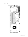
1
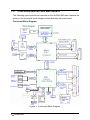
NuPRO-850
Full-Size ePCI-X System
Host Board
Intel® Pentium® 4 processor
User’s Manual
Recycled Paper
© Copyright 2004 ADLINK Technology Inc.
All Rights Reserved.
Manual Rev. 1.00: June 18, 2004
Part Number: 50-13045-100
The information in this document is subject to change without prior notice in
order to improve reliability, design, and function and does not represent a
commitment on the part of the manufacturer.
In no event will the manufacturer be liable for direct, indirect, special,
incidental, or consequential damages arising out of the use or inability to use
the product or documentation, even if advised of the possibility of such
damages.
This document contains proprietary information protected by copyright. All
rights are reserved. No part of this manual may be reproduced by any
mechanical, electronic, or other means in any form without prior written
permission of the manufacturer.
Trademarks
NuDAQ®, NuIPC®, NuDAM®, NuPRO® are registered trademarks of ADLINK
Technology Inc. Other product names mentioned herein are used for
identification purposes only and may be trademarks and/or registered
trademarks of their respective companies.
Getting Service from ADLINK
Customer Satisfaction is top priority for ADLINK Technology Inc. If you need
any help or service, please contact us.
ADLINK TECHNOLOGY INC.
Web Site
http://www.adlinktech.com
Sales & Service
[email protected]
TEL
+886-2-82265877
Address
9F, No. 166, Jian Yi Road, Chungho City, Taipei, 235 Taiwan
FAX
+886-2-82265717
Please email or FAX your detailed information for prompt, satisfactory, and
consistent service.
Detailed Company Information
Company/Organization
Contact Person
E-mail Address
Address
Country
TEL
FAX
Web Site
Questions
Product Model
Environment
Detail Description
Suggestions for ADLINK
OS:
Computer Brand:
M/B:
Chipset:
Video Card:
NIC:
Other:
CPU:
BIOS:
Table of Contents
Chapter 1 Introduction.................................................................. 1
1.1
1.2
1.3
1.4
Unpacking Checklist........................................................................ 2
Features .......................................................................................... 3
Functional Blocks and Main Board .................................................. 4
Specifications .................................................................................. 8
Chapter 2 Jumpers and Connectors ......................................... 11
2.1
2.2
NuPRO-850 Board Outline and Illustration................................... 12
NuPRO-850 Connector Pin Assignments...................................... 14
Chapter 3 Getting Started........................................................... 25
3.1
3.2
3.3
3.4
3.5
CPU Installation ........................................................................... 25
Memory Installation ....................................................................... 26
Connecting IDE Devices to the NuPRO-850 ................................. 27
BIOS Configuration Overview ....................................................... 28
Operating System Installation ....................................................... 29
Chapter 4 Device Driver Installation.......................................... 31
4.1
4.2
Intel® 875P/6300ESB Chipset ...................................................... 31
Driver Installation .......................................................................... 32
Chapter 5 Watchdog Timer......................................................... 35
5.1
Watchdog Timer............................................................................ 35
Chapter 6 ePCI-X Bus Details..................................................... 41
6.1
6.2
6.3
NuPRO-850 ePCI-X Bus ............................................................... 41
Global Signals ............................................................................... 41
PCI-X Bus Signals......................................................................... 42
Warranty Policy ........................................................................... 43
List of Tables and Figures • i
How to Use This Guide
This manual is designed to help users configure the NuPRO-850 Full-Size
ePCI-X System Host Board with Dual Xeon CPU. It is divided into five
chapters.
Chapter 1
Introduction
Gives an overview of the product features, applications, and
specifications.
Chapter 2
Connectors and Jumpers
Outlines all the connectors and its pin definitions.
Chapter 3
Getting Started
Summarization of what is required to setup an operational
system using the NuPRO-850. Hardware installation and BIOS
overview is discussed.
Chapter 4
Driver Installation
Detailed instructions on how to install the software drivers
successfully.
Chapter 5
Utilities
Explains the operation of the WDT, PXE booting, and Hardware
Doctor.
ii • How to Use This Guide
1
Introduction
The NuPRO-850 is a full-size ePCI-X System Host Board (SHB) based on the
Intel® Pentium® 4 processor and 875P Memory Controller Hub / 6300ESB I/O
Controller Hub chipset. It features AGP4X/8X VGA, Serial ATA I/F, Gigabit
Ethernet, and USB v2.0 I/F. It supports two PCI/PCI-X busses via the Intel
6300ESB chipset (one PCI-X 64-bit/66MHz bus and one PCI 32-bit/33MHz
bus). The NuPRO-850 is designed to run under Windows 2000/XP and Linux
operating systems as well as in embedded real time applications.
The NuPRO-850 is a System Host Board with premium computing
performance powered by an Intel® Pentium® 4 processor. The CPU module
supports a front side bus (FSB) of 533/800MHz and a maximum CPU clock
speed of 3.4GHz featuring 64-bit/66MHz PCI/PCI-X bus with up to 4GB high
performance DDR host SDRAM support.
It provides input/output via RS-232, four USB 2.0 ports, Dual IDE Channels
with ATA 100/66/33, Onboard Gigabit Ethernet, and video interfaces for LVDS
Digital LCD Display and dual CRT displays. The NuPRO-850 is designed to
meet the needs of applications which require the highest computing
performance and highest reliability and is designed to run Windows 2000/XP
and Linux operating systems, as well as embedded real-time applications. It is
the ideal solution for telecommunications, internet, and industrial networking
applications.
This chapter is designed to give the user with an overview of the NuPRO-850
SHB. This chapter covers the following topics:
•
Unpacking and Checklist
•
Features
•
Specifications
Introduction • 1
1.1
Unpacking Checklist
Check the shipping carton for any damage. If the shipping carton and contents
are damaged, notify the dealer for a replacement. Retain the shipping carton
and packing materials for inspection by the dealer. Obtain authorization before
returning any product to ADLINK.
Check the following items are included in the package, if there are any items
missing, contact your dealer.
•
The NuPRO-850 module (May be equipped with different speed or
capacity CPU, RAM, and HDD).
•
This User’s Manual
•
ADLINK CD
•
Com Cable
•
Dual Ports USB Cable with bracket
•
1 set of Cooler kits
•
2 x ATA-100 Cables
•
2 x Serial ATA Cables
Note:
The package of the NuPRO-850 OEM version non-standard
configuration may vary in function or contents according to
different configuration requests
CAUTION: This board must be protected from static discharge and
physical shock. Never remove any of the socketed parts except
at a static-free workstation. Use the anti-static bag shipped with
the product to handle the board. Wear a wrist strap grounded
through one of the system's ESD Ground jacks while servicing
system components.
!
2 • Introduction
1.2
Features
•
PICMG 1.2 Rev 1.0 Embedded PCI-X Specification compliant.
•
PCI Local Bus Specification, Rev 2.2 compliant.
•
Single Intel® Pentium® 4 processor with 1MB L2 cache,
533/800MHz FSB, Hyper-Threading Technology.
•
Four 184-pin DIMM sockets, support single/dual channel DDR
DIMM. Up to four DIMMs of DDR 266/333/400 with ECC unbuffered.
Supports a maximum of 4GB of system memory.
•
Intel® 82547GI Gigabit Ethernet Controller. Supports 1000Base-TX,
100Base-TX and 10Base-T (IEEE802.3, 802.3u, and 802.3ab).
•
ATI Mobility M9/M10 with AGP4X/8X compliant, 64MB memory.
LVDS signal output connector supports LVDS Digital LCD Display
and dual CRT displays.
•
AC'97 link Interface, AC’97 2.2 compliant with optional with ADLINK
DB-AC97 board.
•
Supports all generic features include VGA, COM port, USB 2.0,
keyboard, mouse, and hardware monitoring.
•
Built-in monitoring CPU temperatures, FAN speed, system
temperature, CPU voltage, and DC voltages.
•
Supports Intel® Pre-boot Execution Environment (PXE).
•
2 x IDE channels, 2 x SATA ports.
Introduction • 3
1.3
Functional Blocks and Main Board
The following topics provide an overview of the NuPRO-850 main features as
shown in the functional block diagram below and also the main board.
Functional Block Diagram
Figure 1: Functional Block Diagram
4 • Introduction
Main Board Drawing
P
M
A
B
8
7
4
A
G
P
m
Figure 2: Main Board Drawing
Introduction • 5
1.3.1
Intel® Pentium® 4 Processor
The Intel® Pentium® 4 processor is based on Intel® NetBurst®
microarchitecture and built with Intel®'s 0.13-micron and 90nm manufacturing
process and featuring Hyper-Threading technology, a 1MB level two-cache
size. The Intel® Pentium® 4 has a maximum clock speed of 3.4GHz and front
side bus frequency of 400/533/800MHz.
The Intel® NetBurst™ micro-architecture and Hyper-Threading Technology is
designed specifically for multi-tasking environments and provides outstanding
performance for multi-threaded applications.
1.3.2
Video
The NuPRO-850 provides standard SVGA CRT analog output on a bracket I/O
panel. The video function is provided via an ATI Mobility M9 (AGP4X) or M10
(AGP8X) VGA chip with 64MB video memory. NuPRO-850 also supports dual
CRT output (via one onboard 14-pin header) and one LVDS interface. The
NuPRO-850 has one jumper to disable the onboard video and BIOS options
are used to select the resolution of the LVDS panel
1.3.3
Ethernet Interfaces
The NuPRO-850 provides one 10/100/1000Mbps Ethernet interface via the
Intel® 82547GI Gigabit Ethernet Controller. The 82547GI is connected to the
CSA (Communicating Streaming Architecture) interface of the 875P MCH. The
Ethernet interface is routed to a RJ-45 w/LED all-in-one connector on bracket.
The LAN chip will be assigned one unique static MAC Address. LED drive
signals for Ethernet link status and activity are routed to the same connector.
1.3.4
Serial I/O
The NuPRO-850 has one RS-232 serial port with a 10-pin connector. The
16550 compatible serial port is provided by the SIU port on the Intel® 6300ESB
ICH.
1.3.5
Universal Serial Bus (USB)
The NuRPRO-850 supports four USB 2.0 ports, with two connectors (USB0 &
USB1) on bracket and the remaining (USB2 & USB3) routed to one onboard
9-pin header. USB allows for the easy addition of peripherals such as mouse,
keyboard, speakers, etc.
1.3.6
IDE and Serial ATA Controller Controller
The NuPRO-850 provides IDE and Serial ATA interfaces from the Intel®
6300ESB ICH. Two IDE connectors can support up to four drives Ultra DMA
100 Mode. Two serial ATA ports support up to two serial ATA devices for data
transfer rates up to 150Mbps.
6 • Introduction
1.3.7
Software
The NuPRO-850 is compatible with all major PC operating systems. ADLINK
provides support, which may include additional drivers for ADLINK peripherals.
Software device drivers for the NuPRO-850 may be found in the ADLINK CD.
1.3.8
AC’97 Link
NuPRO-850 provides one AC’97 link 10-pin header, the AC’97 link is provided
by the 6300ESB ICH.
1.3.9
Serial I/O
NuPRO-850 provides one RS-232 serial port via one 10-pin connector. The
serial port is provided by the 16550 compatible SIU port in the 6300ESB ICH.
1.3.10 MiniPCI slot
NuPRO-850 provides one MiniPCI type III slot. The MiniPCI slot and ePCI-X
bus B share the 6300ESB PCI bus I/F.
Introduction • 7
1.4
Specifications
Compliant Specifications
•
PICMG 1.2 Rev 1.0 Embedded PCI-X Specification compliant.
•
PCI Local Bus Specification, Rev 2.2 compliant.
Form Factor
•
Standard Full-Size ePCI-X System Host Board, 338.6mm x 122mm
(13.33”x4.8”).
CPU/Cache
•
Intel® Pentium® 4 processor. The socket supports CPUs manufactured
using Intel's 0.13-micron and 90nm manufacturing processes, FC-mPGA4
package (478-pin).
•
The Intel Pentium® 4 processor runs at a core speed of up to 3.4GHz,
with a Front Side Bus (FSB) speed of 400/533/800MHz, and on-die 512KB
or 1MB Advanced Transfer L2 Cache.
®
Chipset
•
Intel 6300ESB I/O Controller Hub
•
Intel® 82875P Memory Controller Hub (MCH)
®
Host Memory
•
Four DDR DIMM sockets
•
266/333/400MHz DDR DIMM modules
•
Dual-channel or single-channel DDR interface
•
Non-ECC and ECC, un-buffered DIMMs only
•
Each socket supports up to 1GB of DDR DIMM
•
128-Mb, 256-Mb, 512Mb technologies implemented as x8, x16 DDR
devices with four banks
•
Up to 4GB system memory
•
Registered DIMMs are not supported
DDR DIMM speed, type and size can be determined by the BIOS reading the
DIMM presence detect bits on the SMBus (System Management Bus). The
8 • Introduction
DDR DIMM timing register, which provides the DIMM speed control for the
entire array, must be programmed to use the timings of the slowest DIMMs
installed. Note: DIMMs must be populated in identical pairs for dual-channel
operation
BIOS: Award / Phoenix BIOS advanced by ADLINK
•
NuPRO-850 supports BIOS memory size up to 8Mbytes (Firmware Hub
I/F).
•
Flash write protection will be implemented under software control. This bit
must be set to 1 before any write will be allowed to the BIOS Flash.
Gigabit Ethernet
•
One 10/100/1000Mbps Ethernet interfaces via the Intel® 82547GI Gigabit
Ethernet Controller. The 82547GI is connected to the CSA
(Communicating Streaming Architecture) interface of the 82875P MCH.
•
Support 1000Base-T, 100Base-TX and 10Base-T (IEEE 802.3, 802.3u,
and 802.3ab).
•
IEEE802.3x compliant flow control, support auto-negotiation and link
setup.
•
Ethernet link status and activity LEDs on the RJ-45 connector.
Graphic Display
•
ATI Mobility M9 (AGP4X) or M10 (AGP8X) VGA chip with 64MB video
memory.
•
Standard SVGA CRT analog output on bracket I/O panel.
•
Also supports 2
LVDS interface.
nd
CRT output (via one onboard 14-pin header) and one
USB Interface
•
Supports four USB 2.0 ports, two connectors (USB0 & USB1) on bracket
and the others (USB2 & USB3) are routed to one onboard 9-pin header
IDE Ports
•
Two IDE connectors support up to four drivers. Up to Ultra DMA 100
Mode.
Super I/O and WDT
•
Built-in HanceRapids, support 2-stage WDT, programmable timer 1 - 255
seconds or 1 - 255 minutes.
Introduction • 9
•
The NuPRO-850 edge connector uses three standard 32-bit PCI
connectors. These three connectors carry two busses, one PCI-X
64-bit/66MHz bus and one PCI 32-bit/33MHz bus. Both busses are
provided by Intel 6300ESB ICH.
Hardware Monitor
•
The W83L784R provides temperature, fans, and voltage monitors. It has
analog to digital converters that allow software to monitor the voltages on
NuPRO-850.
OS Compatibility
•
MS-DOS 6.2+, Windows 2000/XP, Red Hat Linux 7.3 or higher
•
Other OS support available upon request
Environment
•
Operating temperature: 5 to 55 °C
•
Storage temperature: -40 to 70 °C
•
Humidity: 5% to 95% non-condensed
Safety Certificate and Test
•
CE, FCC
•
All plastic material used onboard are all UL-94V certified
10 • Introduction
2
Jumpers and Connectors
This chapter will familiarize the user with the NuPRO-850 with the interfaces and
connections available before getting started. The chapter also contains
information about the board layout, connector definitions and jumper setup as
well as the following information:
•
NuPRO-850 board outline and illustration
•
NuPRO-850 connectors pin assignments
•
NuPRO-850 jumpers setting
Jumpers and Connectors • 11
2.1
2.1.1
NuPRO-850 Board Outline and Illustration
NuPRO-850 Top View
CN16
CN17
LAN1
CN13
CN3
CN6
CN18
CN4
CN9
CN7
ePCI-X bus A
JP1
CN10
CN11
CN12
JPY1
CN1
CN14
CN2
FN1
ePCI-X bus B
PN1
DIMM1
DIMM2
DIMM3
DIMM4
U12
FN2
Figure 3: NuPRO-850 Top View
12 • Jumpers and Connectors
2.1.2
Front View
CN13
LAN1
CN16 CN17
Figure 4: View of Face Plate
Position
CN1
CN2
CN3
CN4
CN6
CN7
CN9
CN10
CN11
CN12
CN13
CN14
CN16
CN17
CN18
LAN1
FN1
FN2
DIMM1
DIMM2
DIMM3
DIMM4
U12
PN1
JP1
JPY1
Description
Case open pin header
Front panel pin header
COM1 connector
Secondary IDE connector
AC’97 link connector
Primary IDE connector
MiniPCI slot
SATA-1 connector
SATA-0 connector
VGA 2nd CRT pin header
VGA CRT connector
LVDS connector
USB-0 connector
USB-1 connector
USB-2/3 pin header
Gigabit Ethernet RJ-45 connector
VGA Fan power connector
CPU Fan power connector
DDR DIMM B1 socket
DDR DIMM B2 socket
DDR DIMM A1 socket
DDR DIMM A2 socket
CPU socket
ATX 12V 4-pin connector
Clear CMOS jumper
VGA disable jumper
Jumpers and Connectors • 13
Table 1: Description of Connector Locations
2.2
NuPRO-850 Connector Pin Assignments
A detailed description and pin-out for each connector is given in the following
section.
2.2.1
VGA CRT connector (CN13)
PIN
1
2
3
4
5
6
7
8
9
10
11
12
SIGNAL
RED
GREEN
BLUE
NC
GND
GND
GND
GND
5VCC
GND
NC
DDC_DATA
13
HSYNC
14
VSYNC
15
DDC_CLK
Table 2: VGA Connector Pin Definition
2.2.2
USB 2.0 connector (CN16, CN17)
Pin #
1
2
3
4
Signal Name
VCC
USBUSB+
Ground
Table 3: USB Connectors Pin Definition
14 • Jumpers and Connectors
FUNCTION
Analog RED
Analog GREEN
Analog BLUE
No Connect
Ground
Ground
Ground
Ground
+5V
Ground
No connect
DDC Data for
CRT
Horizontal sync
for Monitor
Vertical sync for
Monitor
DDC Clock for
CRT
2.2.3
Gigabit Ethernet connector (LAN1)
Green / Orange LED
PIN
1
2
3
4
5
6
7
8
SIGNAL
MDI[0]+
MDI[0]MDI[1]+
MDI[1]MDI[2]+
MDI[2]MDI[3]+
MDI[3]-
Yellow LED
Table 4: Gigabit Ethernet Connector Pin Definition
LED Color
Green / Orange
(Speed status)
Yellow (Link status)
Status
Orange
Green
ON
OFF
Blinking
Function
1000Mbps
100Mbps
Link
No link
Data transfer in progress
Table 5: Ethernet Color LED Status
2.2.4
COM1 connector (CN3)
PIN
1
2
3
4
5
6
7
8
9
10
SIGNAL
DCD
RXD
TXD
DTR
GND
DSR
RTS
CTS
RI
NC
FUNCTION
Data Carrier Detect
Receive Data
Transmit Data
Data Terminal Ready
Ground
Data Set Ready
Request to Send
Clear to Send
Ring Indicate
No Connect
Table 6: Ethernet Color LED Status
Jumpers and Connectors • 15
2.2.5
AC’97 connector (CN6)
PIN
1
2
3
4
5
6
7
8
9
10
SIGNAL
GND
GND
5VCC
5VCC
AC_SYNC
AC_BITCLK
AC_SDIN0
AC_SDOUT
AC_SDIN1
AC_RST#
FUNCTION
Ground
Ground
+5V
+5V
AC’97 Sync
AC’97 Bit Clock
AC’97 Serial Data In 0
AC’97 Serial Data Out
AC’97 Serial Data In 1
AC’97 Reset
Table 7: AC’97 connector (CN6)
2.2.6
Case Open connector (CN1)
Signal is connected to a limit switch sensor of the chassis to detect if the case
is open or closed.
1
PIN
1
2
SIGNAL
CASEOPEN#
GND
FUNCTION
Case Open Signal
Ground
Table 8: Case Open connector Pin Definition
16 • Jumpers and Connectors
2.2.7
VGA 2nd CRT pin header (CN12)
8
1
10
7
PIN
1
2
3
4
5
6
SIGNAL
CRT2_DATA
CRT2_CLK
CRT2_RED
CRT2_GREEN
CRT2_BLUE
CRT2_HSYNC
7
CRT2_VSYNC
8
9
10
11
12
13
14
VCC_CRT2
NC
GND
GND
GND
GND
GND
FUNCTION
DDC Data for CRT2
DDC Clock for CRT2
CRT2 Analog RED
CRT2 Analog GREEN
CRT2 Analog BLUE
CRTR2 Horizontal
sync for Monitor
CRT2 Vertical sync for
Monitor
+5V
No Connect
Ground
Ground
Ground
Ground
Ground
Table 9: VGA 2nd CRT pin header (CN12)
2.2.8
SATA-0 / SATA-1 connectors (CN11, CN10)
CN11: SATA-0
CN10: SATA-1
1
7
PIN
1
2
3
4
5
6
7
SIGNAL
GND
SATA_TXP
SATA_TXN
GND
SATA_RXN
SATA_RXP
GND
FUNCTION
Ground
Serial ATA Transmit
Pair
Ground
Serial ATA Receive
Pair
Ground
Table 10: SATA-0 / SATA-1 connectors (CN11, CN10)
Jumpers and Connectors • 17
2.2.9
LVDS connector (CN14)
PIN
1
2
3
4
5
6
7
8
9
10
11
12
13
14
15
16
17
18
19
20
1
20
SIGNAL
LVDS_PWR
LVDS_PWR
GND
GND
LVDS_L0N
LVDS_L0P
GND
LVDS_L1N
LVDS_L1P
GND
LVDS_L2N
LVDS_L2P
GND
LVDS_LCKN
LVDS_LCKP
GND
LVDS_L3N
LVDS_L3P
GND
GND
FUNCTION
LVDS Power
LVDS Power
Ground
Ground
LVDS lower data channel 0 (-)
LVDS lower data channel 0 (+)
Ground
LVDS lower data channel 1 (-)
LVDS lower data channel 1 (+)
Ground
LVDS lower data channel 2 (-)
LVDS lower data channel 2 (+)
Ground
LVDS lower clock channel (-)
LVDS lower clock channel (+)
Ground
LVDS lower data channel 3 (-)
LVDS lower data channel 3 (+)
Ground
Ground
Table 11: LVDS connector (CN14)
18 • Jumpers and Connectors
2.2.11 ATX 12V 4-pin connector (PN1)
3
1
4
2
PIN
1
2
3
4
SIGNAL
GND
GND
ATX12V
ATX12V
FUNCTION
Ground
Ground
+12V
+12V
Table 12: Floppy Connector Pin Definition
2.2.12 Fan1 / Fan2 connector (FN1/FN2)
3
1
Pin #
1
2
3
Signal Name
GND
Fan power
Fan speed
Table 13: Floppy Connector Pin Definition
Jumpers and Connectors • 19
2.2.13 Primary/Secondary IDE Connector (CN7, CN4)
CN7: Primary IDE
CN4: Secondary IDE
Signal Name
Reset IDE
Host data 7
Host data 6
Host data 5
Host data 4
Host data 3
Host data 2
Host data 1
Host data 0
Ground
DRQ0 / DRQ1
Host IOW
Host IOR
IOCHRDY
DACK0 / DACK1
IRQ14 / IRQ 15
Address 1
Address 0
Chip select 0
Activity
Pin #
1
3
5
7
9
11
13
15
17
19
21
23
25
27
29
31
33
35
37
39
Pin #
2
4
6
8
10
12
14
16
18
20
22
24
26
28
30
32
34
36
38
40
Signal Name
Ground
Host data 8
Host data 9
Host data 10
Host data 11
Host data 12
Host data 13
Host data 14
Host data 15
No connect
Ground
Ground
Ground
Host ALE
Ground
No connect
No connect
Address 2
Chip select 1
Ground
Table 14: IDE Connector Pin Definition
20 • Jumpers and Connectors
2.2.14 Front Panel Pin Header (CN2)
1
10
PI
N
1
2
SIGNAL
FUNCTION
+5V
WDTLED#
3
PLED
4
5
6
7
8
NC
GND
GND
NC
PWRON
9
+5VSB
10
PME#
(Optional)
11
WDSPK
12
13
14
15
NC
NC
+5V
RESETBT
16
17
GND
HDDLED
18
19
+5V
PWRBT
20
GND
Power
Watch Dog
LED Signal
Power LED
Signal
No Connect
Ground
Ground
No connect
Power-on
signal
+5V Standby
Power
Power
Management
Event
Speaker
signal
No connect
No connect
Power
RESET
Button signal
Ground
Hard Disk
LED signal
Power
POWER
Button signal
Ground
PIN
GROUP
Power
LED
Key Lock
ATX
Power
connector
Chassis
Speaker
RESET
button
Hard Disk
LED
Power on
button
Table 15: Front Panel Pin Definition
Jumpers and Connectors • 21
2.2.15 Mini PCI Socket (CN9)
PIN
SIGNAL
1
3
5
7
9
11
13
15
17
19
21
23
25
27
29
31
33
35
37
39
41
43
45
47
49
51
53
55
57
59
61
NC
NC
NC
NC
NC
NC
NC
GND
INTB#
+3.3V
EX_CLK
GND
CLK
GND
REQ#
+3.3V
AD[31]
AD[29]
GND
AD[27]
AD[25]
EX_IDSEL#
C/BE[3]
AD[23]
GND
AD[21]
AD[19]
GND
AD[17]
C/BE[2]
IRDY#
22 • Jumpers and Connectors
PIN
2
4
6
8
10
12
14
16
18
20
22
24
26
28
30
32
34
36
38
40
42
44
46
48
50
52
54
56
58
60
62
SIGNAL
NC
NC
NC
NC
NC
NC
NC
EX_INTC#
+5V
INTA#
EX_INTD#
+3.3VS
RESET#
+3.3V
GNT#
GND
PME#
EX_REQ#
AD[30]
+3.3V
AD[28]
AD[26]
AD[24]
IDSEL#
GND
AD[22]
AD[20]
PAR
AD[18]
AD[16]
GND
63
65
67
69
71
73
75
77
79
81
83
85
87
89
91
93
95
97
99
101
103
105
107
109
111
113
115
117
119
121
123
+3.3V
CLKRUN#
SERR#
GND
PERR#
C/BE[1]
AD[14]
GND
AD[12]
AD[10]
GND
AD[8]
AD[7]
+3.3V
AD[5]
EX_GNT#
AD[3]
+5V
AD[1]
GND
AC_SYNC
AC_SDIN
AC_BITCLK
AC_ID1#
NC
NC
NC
NC
NC
NC
+5Analog
64
66
68
70
72
74
76
78
80
82
84
86
88
90
92
94
96
98
100
102
104
106
108
110
112
114
116
118
120
122
124
FRAME#
TRDY#
STOP#
+3.3V
DEVSEL#
GND
AD[15]
AD[13]
AD[11]
GND
AD[9]
C/BE[0]
+3.3V
AD[6]
AD[4]
AD[2]
AD[0]
SMBCLK
SMBDATA
GND
GND
AC_SDOUT
AC_ID0#
AC_RST#
NC
GND
NC
NC
NC
NC
+3.3VSB
Table 16: Mini PCI Socket Pin Definition
Jumpers and Connectors • 23
3
Getting Started
This chapter gives a summary of what is required to setup an operational
system using the NuPRO-850, including hardware installation and an overview
of the BIOS.
3.1
CPU Installation
The NuPRO-850 CPU module supports single/dual FC-mPGA2 Intel®
Pentium® 4 processor with a front side bus (FSB) of 800MHz or 533MHz.
Users need to install highly efficient CPU fan/cooler to guarantee the systems
stability.
To install the CPU follow the steps below carefully:
1.
Lift the lever on the CPU socket.
2.
Insert the CPU in the socket, making sure that pin 1 of the CPU aligns
with pin 1 of the socket (both corners are marked with a triangle)
3.
Press the lever down until you hear it “click” into the locked position.
4. Apply the proper amount of thermal compound to the CPU die and
place the heatsink and fan on top of the CPU.
5.
Connect the three wires of the CPU fan to the respective CPU fan
connector.
Note:
Ensure that the CPU heat sink and the CPU top surface are in
tight contact to avoid CPU overheating problem that would
cause your system to hang or crash. The CPU heat sink and fan
should be installed tightly together. Please contact ADLINK
dealers for suitable heat sink and fan assemblies
Getting Started • 25
3.2
Memory Installation
This section details the procedure for installing system memory on the
NuPRO-850. Correct memory configuration is critical for proper system
operation.
3.2.1
Memory Configuration Options
The NuPRO-850 has flexible memory configuration options. These include
support for 64MB, 128MB, 256MB, 512MB, 1GB Modules. Note that the
modules must all be the of the same type and density and must be installed in
pairs (DIMM1 and SIMM2 or DIMM3 and DIMM4) for dual-channel mode
operation.
Figure 5: DIMM Sockets
3.2.2
Installing Memory Modules
Installing DIMM modules is simple. The modules insert in the sockets and are
held in place by the socket retaining arms. The edge connectors on the
modules are of different widths and there are key notches in each module.
These ensure that you do not insert a module incorrectly.
Before installing any modules, a configuration should be chosen. The required
number and type of DDR modules should then be prepared.
26 • Getting Started
To install either types of module, follow these procedures:
Figure 6: Inserting DIMM into Socket
3.3
1.
Align the module to the socket so that the edge connectors on the
module match the socket sections.
2.
Hold the module perpendicular to the motherboard and press the
edge connector into the socket.
3.
Press the module fully into the socket so that the socket retaining
arms swing up and engage the retention notches at each end of the
module.
4.
Following the configuration chosen, repeat for all other modules (if
any).
5.
Once the modules are installed, system memory installation is
complete.
Connecting IDE Devices to the NuPRO-850
The NuPRO-850 supports two IDE channels, Primary and Secondary. It has
two IDE device connectors onboard supporting IDE devices running in any
data transfer mode up to ATA-100. Each IDE connector supports two drives, a
Master and a Slave. The drives connect to the NuPRO-850 with an IDE ribbon
cable.
To install an IDE drive, connect the drive to one of the drive connectors to a
suitable ribbon cable. Plug the board end of the cable into one of the IDE
connectors on the NuPRO-850. Make sure pin 1 of the ribbon cable connector
is aligned with pin 1 of the IDE device connector.
Getting Started • 27
3.4
BIOS Configuration Overview
This section gives an introduction to the Phoenix/Award Plug and Play BIOS
Setup Utility. For more detailed information about the BIOS and other utilities,
please refer to the BIOS Manual.
The BIOS has many separately configurable features. These features are
selected by running the built-in Setup utility. System configuration settings are
saved in a portion of the battery-backed RAM in the real-time clock device and
are used by the BIOS to initialize the system at boot up or reset. The
configuration is protected by a checksum word for system integrity.
To access the Setup utility, press the "Del" key during system RAM check at
boot time. When Setup runs, an interactive configuration screen displays.
Setup parameters are divided into different categories. The available
categories are listed in a menu. The parameters within the highlighted (current)
category are listed in the bottom portion of the Setup screen. Context sensitive
help is displayed in the right portion of the screen for each parameter.
Use the arrow keys to select a category from the menu. To display a submenu,
highlight the category and then press the "Enter" key.
28 • Getting Started
3.5
Operating System Installation
For more detailed information about your operating system, refer to the
documentation provided by the operating system vendor.
Install peripheral devices. NuPRO devices are automatically configured by the
BIOS during the boot sequence.
Most operating systems require initial installation on a hard drive from a floppy
or CDROM drive. These devices should be configured, installed, and tested
with the supplied drivers before attempting to load the new operating system.
Read the release notes and installation documentation provided by the
operating system vendor. Be sure to read any README files or documents
provided on the distribution disks, as these typically note documentation
discrepancies or compatibility problems.
Select the appropriate boot device order in the SETUP boot menu depending
on the OS installation media used. For example, if the OS includes a bootable
installation floppy, select Floppy as the first boot device and reboot the system
with the installation floppy installed in the floppy drive. (Note that if the
installation requires a non-bootable CD-ROM, it is necessary to boot an OS
with the proper CD-ROM drivers in order to access the CD-ROM drive).
Proceed with the OS installation as directed, be sure to select appropriate
device types if prompted. Refer to the appropriate hardware manuals for
specific device types and compatibility modes of ADLINK NuIPC products.
When installation is complete, reboot the system and set the boot device order
in the SETUP boot menu appropriately.
Getting Started • 29
4
Device Driver Installation
To install drivers for the NuPRO-850, refer to the installation information in this
chapter. Basic driver installation information for Windows XP/2000 is outlined
in this section. For installation information for non-Windows Operating
Systems, refer to the extensive explanations on the ADLINK CD. The drivers
are located in the following directories of the CD-Rom:
Chipset driver
\NuPRO\NuPRO-850\chipset
LAN relative driver
\NuPRO\NuPRO-850\LAN
WDT
\NuPRO\NuPRO-850\
4.1
Intel® 875P/6300ESB Chipset
This section describes the installation procedure for the Intel® 6300ESB
chipset device driver under Windows 2000/XP.
4.1.1
System Requirements
One of the following operating systems must be fully installed on the system
before installing any other driver, utilities, or software:
¾
Windows® 2000
¾
®
Windows XP
Device Driver Installation • 31
4.1.2
Hardware Configuration File Installation
This section describes how to install the hardware configuration files into a
system operating Windows 2000/XP.
1.
Check the System Requirements. Windows 2000/XP must be fully
installed and running on the system prior to running this software.
2.
Close any running applications.
3.
The files are stored in an integrated application setup program. This
program is designed for a Windows 2000/XP and can be executed from
the Run command prompt.
4.
Place the ADLINK CD into the CD-ROM drive. Run Setup.exe under
X:\NuPRO\NuPRO-850\chipset. Where X is the CD drive letter.
5.
The user will be prompted with a license agreement. Should the user not
agree with the terms and conditions for using the software, the Installer will
exit before extracting any files.
6.
Follow the on-screen instructions and use the default settings to complete
the setup, once the operating system has rebooted. This completes the
installation of the Intel® Chipset Software Installation Utility.
4.2
Driver Installation
4.2.1
VGA Driver Installation
Windows 2000/XP will attempt to install a standard VGA driver automatically.
To guarantee compatibility, manually install the most updated VGA driver,
which is stored in the ADLINK CD. After installing Windows 2000/XP, update to
the most updated driver by following these steps:
1.
Boot Windows 2000/XP, then run the program
\NuPRO\NuPRO-850\VGA\SETUP.EXE
2.
The VGA driver will automatically be installed onto the system.
3.
Restart the system.
32 • Driver Installation
4.2.2
LAN Driver Installation
This section describes the LAN driver installation process for the Intel® 82547
Gigabit Ethernet controller under Windows 2000/XP. The Intel® software
utilities package include Diagnostics utility; Makedisk utility; and
10/100/1000Mbps Ethernet device drivers. All drivers and utilities are stored in
the ADLINK CD under the directory: X:\NuPRO\NuPRO-850\LAN, where X: is
the location of the CD-ROM drive. For driver installations of other OS, please
refer to the readme file on the CD.
The installation procedures for Windows 2000/XP are the same. During
Windows 2000/XP installation, the operating system will install a LAN driver
automatically. It is recommended that the most updated LAN driver be
installed, which is shipped with the ADLINK CD. This will ensure total
compatibility. After installing the OS, update to the newer driver by following
these steps:
1.
Run the self-extracting pro2kxpm.exe file. The extracted files are stored
to the default location C:\IntelPRO.
2.
To install or update the Ethernet drivers for the system, click ‘Install Now’.
All Ethernet devices on the computer will be updated.
3.
Reboot the system for the new drivers to take effect.
Note:
To check if there are newer updates of the drive, it is
recommended
that
the
following
website
http://www.intel.com/design/software/driver/platform/
be
checked out on a regular basis.
Device Driver Installation • 33
5
Watchdog Timer
5.1
Watchdog Timer
The operation of the Nupro-850’s watchdog timer is described in this chapter.
An overview of the watchdog operation and features, as well as the
programming procedure is provided to give the user an insight into the
workings of the watchdog timer.
5.1.1
WDT Overview
The primary function of the watchdog timer is to monitor the Nupro-850’s
operation and to generate IRQ or to reset the system should the software fail to
function as programmed. The major features of the watchdog timer are:
z Enabled and disabled through software control
z Armed and strobed through software control
The Nupro-850’s custom watchdog timer circuit is integrated in the south
bridge 6300ESB.
Watchdog Timer • 35
The Intel 6300ESB ICH includes a two-stage Watchdog Timer (WDT) that
provides a resolution that ranging from 1 micro second to 10 minutes. The
timer uses a 35-bit Down-Counter. The counter is loaded with the value from
the first Preload register. The timer is then enabled and starts counting down.
The time at which the WDT first starts counting down is called the first stage. If
the host fails to reload the WDT before the 35-bit down counter reaches zero
the WDT generates an internal interrupt. After the interrupt is generated, the
WDT loads the value from the second Preload register into the WDT’s 35-bit
Down-Counter and starts counting down. The WDT is now in second stage. If
the host still fails to reload the WDT before the second timeout, the WDT drives
the WDT_TOUT# pin low. The WDT_TOUT# pin is held low until the system is
reset.
The WDT of 6300ESB also supports multiple modes, WDT and free-running.
Free-running mode is a one stage timer and it will toggle WDT_TOUT# after
programmable time. WDT mode is a two stage timer and its operation is
described as above.
5.1.2
Configuration Registers
The Intel® 6300ESB ICH WDT, appears to BIOS as PCI Bus 0, Device 29,
Function 4, and has the standard set of PCI Configuration register. The
following describes the configuration registers.
Offset 10H: Base Address Register (BAR)
This register determines the memory base for WDT down-counter setting. It
will be used to set Preload value 1 register, Preload value 2 register, General
Interrupt Status register and Reload register.
Preload Value 1 & 2 registers
These two registers are used to hold the preload value for the WDT timer. Its
value will be automatically transferred into the down-counter every time the
WDT enters the first and second stage. Preload Value 1 register is located at
Base + 00H and Preload Value 2 register is located at Base + 04H. Only bit
[19:0] are settable.
The register unlocking sequence is necessary whenever writing to the Preload
registers. Instructions for writing a value into preload value 1&2 register are as
follows:
1. Write 80H to offset BAR + 0CH.
2. Write 86H to offset BAR + 0CH.
3. Write desired value to preload register. (BAR + 00H or BAR + 04H)
36 • Watchdog Timer
General Interrupt Status Register
This register is at Base + 08H. Bit 0 is set when the first stage of down-counter
reaches zero.
Bit 0 = 0 – No Interrupt
Bit 1 = 1 – Interrupt Active
NOTE: This bit is not set in free-running mode.
Reload Register
This register is at Base + 0CH. Write 1 to bit 8 will reload the down-counter’s
value. To prevent a timeout:
1.
Write 80H to offset BAR + 0CH
2.
Write 86H to offset BAR + 0CH
3.
Write a ‘1’ to RELOAD[8] of the reload register
Offset 60 – 61H: WDT Configuration Register
Bit 5 indicates whether or not the WDT will toggle the WDT_TOUT# pin when
WDT times out. (0 = Enabled, 1 = Disabled)
Bit 2 provides two options for prescaling the main down-counter. (0 = 1ms –
10min, 1 = 1us – 1sec)
Bit [1:0] allows the user to choose the type of interrupt desired when the WDT
reached the end of the first stage without being reset. (00 = IRQ, 01 = reserved,
10 = SMI, 11 = Disabled)
NOTE: The WDT does not support SMI now. IRQ uses APIC 1, INT 10 and it is
active low, level triggered.
Offset 68H: WDT Lock Register
Bit 2 is used to choose the functionality of the timer. (0 = Watchdog Timer
mode, 1 = Free running mode) The free-running mode ignores the first stage
and only uses Preload Value 2. In free-running mode it is not necessary to
reload the timer as it is done automatically every time the down-counter
reaches zero.
Bit 1 enables or disables the WDT. (0 = Disabled, 1 = Enabled)
Bit 0 will lock the values of this register until a hard reset occurs or power is
cycled. (0 = unlocked, 1 = locked) The default is Unlocked.
Watchdog Timer • 37
5.1.2
GPIO Control Registers
There are two GPIOs on Nupro-850 that relate to watchdog timer. They are
listed below. The GPIO control base port is 480H.
WDT_TOUT# pin selection
WDT_TOUT# signal is multiplexed with GPIO32. When using WDT, this signal
must be switched to WDT_TOUT# function. It used bit 0 of GPIOBASE + 30H
to set WDT_TOUT function. (0 = WDT_TOUT#, 1 = GPIO32)
WDT LED Control
GPO25 of 6300ESB is designed to control WDT LED. Two features of WDT
LED are supported on Nupro-850’s WDT LED lights or blinks.
WDT LED light
Set bit 25 of GPIOBASE + 04H to 0. Bit 25 of GPIOBASE + 0CH determines
the state of WDT LED. (0 = light, 1 = dark)
WDT LED blink
Set bit 25 of GPIOBASE + 04H to 0. Bit 25 of GPIOBASE + 18H enables WDT
LED blinking function. (0 = function normally, 1 = enable blinking) The high and
low times have approximately 0.5 seconds each.
5.1.3
The procedure of programming WDT
Step 1:
Make sure WDT_TOUT# signal is workable. (Not GPIO32 function).
Step 2:
Set WDT output enable, presecaler and interrupt type into WDT
configuration register.
Step 3:
Get control base from Base Address register.
Step 4:
Program Preload register’s value according to unlocking sequence.
Step 5:
Set WDT timer mode into WDT Lock Register.
Step 6:
Enable WDT from WDT Lock register and program which
functionality of WDT LED will be.
To keep the timer from causing an interrupt or driving WDT_TOUT#, the timer
must be reloaded periodically. The frequency of reloads required is dependent
on the value of the preload values. To reload the down-counter, the register
unlocking sequence must be performed.
To disable WDT, Set bit 1 of WDT Lock Register to 0.
38 • Watchdog Timer
5.1.4
Utilities
ADLINK provides a demo DOS utility, HRWDT.EXE. It is included in the driver
CD. Run “hrwdt /?” under the following directory:
X:\CHIPDRV\WDT\HRWDT for a more detailed explanation.
User also can download the Intel WDT demo windows application from Intel
driver download center.
Watchdog Timer • 39
6
ePCI-X Bus Details
6.1
NuPRO-850 ePCI-X Bus
The NuPRO-850 provides PCI-X/PCI buses. Bus-A can run up to 64-bit PCI-X
66. Bus-B can run PCI 33MHz.
The ePCI-X Bus pin assignment is compatible with the PICMG 1.2 ePCI-X
specifications. In the following sections, we will describe the detail signal
definition and the design guide for the backplane designer to be compatible
with the NuPRO-850 ePCI-X bus.
6.2
6.2.1
Global Signals
Standby Supply (+3.3Vaux)
The NuPRO-850 onboard circuit generate 3.3Vaux power from the +5Vaux or
+5V. Therefore, NuPRO-850 does not require the backplane to provide
+3.3Vaux.
6.2.2
ATX Support
The ATX support signals include PWRGD, PSON#, PWRBT#, +5Vaux. The
NuPRO-850 design provides the ATX power control capability.
If the backplane did not provide the +5Vaux, then the PWRBT# and PSON#
will not work under ATX power mode. Users have to setup the external wiring to
switch on/off the power supply.
6.2.3
JTAG
NuPRO-850 does NOT implement the JTAG signals.
6.2.4
I2C Bus
The onboard SMBus is connected to the SER_SCL and SER_SDA pins.
ePCI-X Bus Details • 41
6.2.5
PME#
The NuPRO-850 implement PME# signal and connect it to 6300ESB
6.3
6.3.1
PCI-X Bus Signals
Backplane Present
The a_PRSNT# and b_PRSNT# signals are connected to the super I/O chip’s
GP25 and GP26 pins respectively. These signal are pulled to +3.3V via 4.7k
resistors.
6.3.2
VIO Electrical Keying
NuPRO-850 monitors the VIO keying signals from backplane.
6.3.3
M66EN and PCIXCAP
The Bus-A supports up to PCI-X 66, the M66EN, and PCIXCAP of Bus-A and
Bus-B can be used to program the PCI mode.
42 • ePCI-X Bus Details
Warranty Policy
Thank you for choosing ADLINK. To understand your rights and enjoy all the
after-sales services we offer, please read the following carefully.
1.
Before using ADLINK’s products please read the user manual and follow the
instructions exactly. When sending in damaged products for repair, please
attach an RMA application form which can be downloaded from:
http://rma.adlinktech.com/policy/.
2.
All ADLINK products come with a limited two-year warranty, one year for
products bought in China.
3.
•
The warranty period starts on the day the product is shipped from
ADLINK’s factory.
•
Peripherals and third-party products not manufactured by ADLINK
will be covered by the original manufacturers' warranty.
•
For products containing storage devices (hard drives, flash cards,
etc.), please back up your data before sending them for repair.
ADLINK is not responsible for any loss of data.
•
Please ensure the use of properly licensed software with our
systems. ADLINK does not condone the use of pirated software
and will not service systems using such software. ADLINK will not
be held legally responsible for products shipped with unlicensed
software installed by the user.
•
For general repairs, please do not include peripheral accessories. If
peripherals need to be included, be certain to specify which items
you sent on the RMA Request & Confirmation Form. ADLINK is not
responsible for items not listed on the RMA Request &
Confirmation Form.
Our repair service is not covered by ADLINK's guarantee in the following
situations:
•
Damage caused by not following instructions in the User's Manual.
•
Damage caused by carelessness on the user's part during product
transportation.
•
Damage caused by fire, earthquakes, floods, lightening, pollution,
other acts of God, and/or incorrect usage of voltage transformers.
•
Damage caused by inappropriate storage environments such as
with high temperatures, high humidity, or volatile chemicals.
•
Damage caused by leakage of battery fluid during or after change
of batteries by customer/user.
Warranty Policy • 43
4.
•
Damage from
technicians.
•
Products with altered and/or damaged serial numbers are not
entitled to our service.
•
This warranty is not transferable or extendible.
•
Other categories not protected under our warranty.
improper
repair
by
unauthorized
ADLINK
Customers are responsible for all fees necessary to transport damaged
products to ADLINK.
For further questions, please e-mail our FAE staff: [email protected]
44 • Warranty Policy