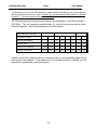
1
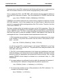
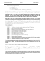
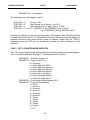
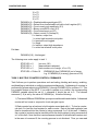
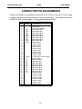
ACCES I/O PRODUCTS INC
10623 Roselle St., San Diego, CA 92121
Tel (619) 550-9559 FAX (619) 550-7322
COUNTER TIMER CARD
CTR-05
USER MANUAL
file: MCTR-05.B3c
COUNTER TIMER CARD
CTR-05
USER MANUAL
NOTICES
The information in this document is provided for reference only. ACCES I/O PRODUCTS
INC does not assume any liability arising out of the application or use of the information
or products described herein. This document may contain or reference information and
products protected by copyrights or patents and does not convey any license under the
patent rights of ACCES, nor the rights of others.
IBM PC, PC/XT, and PC/AT are registered trademarks of the International Business
Machines Corporation.
Printed in USA. Copyright 1993 by ACCES I/O PRODUCTS INC, 16023 Roselle Street,
San Diego,CA 92121. All rights reserved.
COUNTER TIMER CARD
CTR-05
USER MANUAL
TABLE OF CONTENTS
INSTALLATION . . . . . . . . . . . . . . . . . . . . . . . . . . . . . . . . . . . . . . . . . . . . . . . . . . . . . . .
CD INSTALLATION . . . . . . . . . . . . . . . . . . . . . . . . . . . . . . . . . . . . . . . . . . . .
3.5-INCH DISKETTE INSTALLATION . . . . . . . . . . . . . . . . . . . . . . . . . . . . . .
DIRECTORIES CREATED ON THE HARD DISK . . . . . . . . . . . . . . . . . . . . .
INSTALLING THE CARD . . . . . . . . . . . . . . . . . . . . . . . . . . . . . . . . . . . . . . .
1-1
1-1
1-1
1-2
1-5
FUNCTIONAL DESCRIPTION . . . . . . . . . . . . . . . . . . . . . . . . . . . . . . . . . . . . . . . . . . . .
COUNTERS . . . . . . . . . . . . . . . . . . . . . . . . . . . . . . . . . . . . . . . . . . . . . . . . .
CRYSTAL TIMEBASE . . . . . . . . . . . . . . . . . . . . . . . . . . . . . . . . . . . . . . . . . .
DIGITAL I/O . . . . . . . . . . . . . . . . . . . . . . . . . . . . . . . . . . . . . . . . . . . . . . . . .
INTERRUPTS . . . . . . . . . . . . . . . . . . . . . . . . . . . . . . . . . . . . . . . . . . . . . . . .
SOFTWARE . . . . . . . . . . . . . . . . . . . . . . . . . . . . . . . . . . . . . . . . . . . . . . . . .
2-1
2-1
2-1
2-2
2-2
2-2
BLOCK DIAGRAM . . . . . . . . . . . . . . . . . . . . . . . . . . . . . . . . . . . . . . . . . . . . . . . . . . . . . 2-3
ADDRESS ASSIGNMENTS FOR 286/386/486 COMPUTERS . . . . . . . . . . . 3-1
OPTION SELECTION . . . . . . . . . . . . . . . . . . . . . . . . . . . . . . . . . . . . . . . . . . . . . . . . . .
CRYSTAL TIMEBASE . . . . . . . . . . . . . . . . . . . . . . . . . . . . . . . . . . . . . . . . . .
SYNCHRONIZATION . . . . . . . . . . . . . . . . . . . . . . . . . . . . . . . . . . . . . . . . . .
READ/WRITE PULSE WIDTH . . . . . . . . . . . . . . . . . . . . . . . . . . . . . . . . . . .
INTERRUPTS . . . . . . . . . . . . . . . . . . . . . . . . . . . . . . . . . . . . . . . . . . . . . . . .
4-1
4-1
4-1
4-1
4-1
OPTION SELECTION MAP . . . . . . . . . . . . . . . . . . . . . . . . . . . . . . . . . . . . . . . . . . . . . . 4-2
SOFTWARE . . . . . . . . . . . . . . . . . . . . . . . . . . . . . . . . . . . . . . . . . . . . . . . . . 5-1
INTRODUCTION . . . . . . . . . . . . . . . . . . . . . . . . . . . . . . . . . . . . . . . . . . . . . . 5-1
LOADING THE CALL ROUTINE . . . . . . . . . . . . . . . . . . . . . . . . . . . . . . . . . . 5-1
CALL STATEMENT FORMAT . . . . . . . . . . . . . . . . . . . . . . . . . . . . . . . . . . . . 5-2
TASK SUMMARY
. . . . . . . . . . . . . . . . . . . . . . . . . . . . . . . . . . . . . . . . . . . 5-3
TASK 0 INITIALIZE & SET MASTER MODE REGISTER . . . . . . . . . . . 5-3
TASK 1 SET A COUNTER MODE REGISTER . . . . . . . . . . . . . . . . . . 5-5
TASK 2 MULTIPLE COUNTER CONTROL COMMANDS . . . . . . . . . . . 5-6
TASK 3 LOAD COUNTER LOAD REGISTER . . . . . . . . . . . . . . . . . . . 5-8
TASK 4 READ SELECTED COUNTER HOLD REGISTER . . . . . . . . . 5-8
TASK 5 READ THE DIGITAL INPUT PORT . . . . . . . . . . . . . . . . . . . . 5-9
TASK 6 WRITE TO DIGITAL OUTPUT PORT . . . . . . . . . . . . . . . . . . . 5-9
TASK 7 LATCH COUNTERS AND SAVE ON INTERRUPT . . . . . . . . 5-10
TASK 8 RETURN STATUS OF INTERRUPTS . . . . . . . . . . . . . . . . . 5-12
TASK 9 TRANSFER DATA DURING/AFTER INTERRUPT . . . . . . . . . 5-13
TASK 10 MEASURE FREQUENCY . . . . . . . . . . . . . . . . . . . . . . . . . . 5-14
SUMMARY OF ERROR CODES . . . . . . . . . . . . . . . . . . . . . . . . . . . . . 5-16
PROGRAMMING IN OTHER LANGUAGES . . . . . . . . . . . . . . . . . . . . . . . . 5-17
PROGRAMMING . . . . . . . . . . . . . . . . . . . . . . . . . . . . . . . . . . . . . . . . . . . . . . . . . . . . . .
I/O ADDRESSES . . . . . . . . . . . . . . . . . . . . . . . . . . . . . . . . . . . . . . . . . . . . .
BYTE-ORIENTED OPERATION . . . . . . . . . . . . . . . . . . . . . . . . . . . . . . . . . .
9513 REGISTER FUNCTIONS . . . . . . . . . . . . . . . . . . . . . . . . . . . . . . . . . . .
COMMAND REGISTER . . . . . . . . . . . . . . . . . . . . . . . . . . . . . . . . . . . . .
i
6-1
6-1
6-1
6-1
6-2
COUNTER TIMER CARD
CTR-05
USER MANUAL
DATA POINTER REGISTER . . . . . . . . . . . . . . . . . . . . . . . . . . . . . . . . .
MASTER MODE REGISTER . . . . . . . . . . . . . . . . . . . . . . . . . . . . . . . . .
COUNTER MODE REGISTER . . . . . . . . . . . . . . . . . . . . . . . . . . . . . . .
DIGITAL INPUT/OUTPUT . . . . . . . . . . . . . . . . . . . . . . . . . . . . . . . . . . . . . . .
INTERRUPT INPUT . . . . . . . . . . . . . . . . . . . . . . . . . . . . . . . . . . . . . . . . . . .
6-3
6-5
6-7
6-9
6-9
CALIBRATION . . . . . . . . . . . . . . . . . . . . . . . . . . . . . . . . . . . . . . . . . . . . . . . 7-1
CONNECTOR PIN ASSIGNMENTS . . . . . . . . . . . . . . . . . . . . . . . . . . . . . . . . . . . . . . . . 8-1
SPECIFICATION . . . . . . . . . . . . . . . . . . . . . . . . . . . . . . . . . . . . . . . . . . . . . . . . . . . . . . 9-1
WARRANTY . . . . . . . . . . . . . . . . . . . . . . . . . . . . . . . . . . . . . . . . . . . . . . . . 10-1
LSI TYPE 9513 DATA SHEET . . . . . . . . . . . . . . . . . . . . . . . . . . . . . . . . . . . . . . . . . . . . A-1
ii
COUNTER TIMER CARD
CTR-05
USER MANUAL
INSTALLATION
The software provided with this card is contained on either one CD or multiple diskettes
and must be installed onto your hard disk prior to use. To do this, perform the following
steps as appropriate for your software format and operating system. Substitute the
appropriate drive letter for your CD-ROM or disk drive where you see d: or a:
respectively in the examples below.
CD INSTALLATION
DOS/WIN3.x
1. Place the CD into your CD-ROM drive.
2. Type d:K to change the active drive to the CD-ROM
drive.
3. Type installK to run the install program.
4. Follow the on-screen prompts to install the software for
this card.
WIN95/98/NT
1. Place the CD into your CD-ROM drive.
2. The CD should automatically run the install program after 30 seconds.
If the install program does not run, click START | RUN and type
d:install, click OK or press K.
3. Follow the on-screen prompts to install the software for this card.
4. Click the “Go to ACCES Web” button to check for software updates.
3.5-INCH DISKETTE INSTALLATION
As with any software package, you should make backup copies for everyday use and
store your original master diskettes in a safe location. The easiest way to make a
backup copy is to use the DOS DISKCOPY utility.
In a single-drive system, the command is:
diskcopy a: a:K
You will need to swap disks as requested by the system.
In a two-disk system, the command is:
diskcopy a: b:K
This will copy the contents of the master disk in drive A to the backup disk in drive B.
1-1
COUNTER TIMER CARD
CTR-05
USER MANUAL
To copy the files on the master diskette to your hard disk, perform the following steps.
1.
Place the master diskette into a floppy drive
2.
Change the active drive to the drive that has the diskette installed. For
example, if the diskette is in drive A, type a:K.
3.
Type installK and follow the on-screen prompts.
DIRECTORIES CREATED ON THE HARD DISK
The installation process will create several directories on your hard disk. If you accept
the installation defaults, the following structure will exist.
[CARDNAME]
Root or base directory containing the SETUP.EXE setup program
used to help you configure jumpers and calibrate the card.
DOS\PSAMPLES:
A subdirectory of [CARDNAME] that contains Pascal
samples.
DOS\CSAMPLES:
A subdirectory of [CARDNAME] that contains “C” samples.
WIN32\language
Subdirectories containing samples for Win95/98 and
NT.
WinRisc.exe: A Windows dumb-terminal type communication program designed for RS422/485 operation. Used primarily with
REMOTE ACCES Data Acquisition Pods and our RS422/485 serial
communication product line. Can be used to say hello to an installed modem.
ACCES32:
This directory contains the Windows 95/98/NT driver used to provide
access to the hardware registers when writing 32-bit Windows software. Several samples are provided in a variety of languages to
demonstrate how to use this driver. The DLL provides four functions
(InPortB, OutPortB, InPort, and OutPort) to access the hardware.
This directory also contains the device driver for Windows NT,
ACCESNT.SYS. This device driver provides register-level hardware
access in Windows NT. Two methods of using the driver are
available, through ACCES32.DLL (recommended) and through the
DeviceIOControl handles provided by ACCESNT.SYS (slightly faster).
SAMPLES: Samples for using ACCES32.DLL are provided in this
directory. Using this DLL not only makes the hardware
programming easier (MUCH easier), but also one
source file can be used for both Windows 95/98 and
1-2
COUNTER TIMER CARD
CTR-05
USER MANUAL
WindowsNT. One executable can run under both
operating systems and still have full access to the
hardware registers. The DLL is used exactly like any
other DLL, so it is compatible with any language
capable of using 32-bit DLLs. Consult the manuals
provided with your language’s compiler for information
on using DLLs in your specific environment.
VBACCES:
PCI:
This directory contains sixteen-bit DLL drivers for use
with VisualBASIC 3.0 and Windows 3.1 only. These
drivers provide four functions, similar to the
ACCES32.DLL. However, this DLL is only compatible
with 16-bit executables. Migration from 16-bit to 32-bit
is simplified because of the similarity between
VBACCES and ACCES32.
This directory contains PCI-bus specific programs and information. If
you are not using an ACCES PCI card, this directory will not be
installed.
SOURCE:
A utility program is provided with source code you can
use to determine allocated resources at run-time from
your own programs in DOS.
PCIFind.exe A utility for DOS and Windows to determine what base
address and IRQ are allocated to installed PCI cards.
This program runs two versions, depending on the
operating system. Windows 95/98/NT displays a GUI
interface, and modifies the registry. When run from
DOS or Windows3.x, a text interface is used. For
information about the format of the registry key, consult
the card-specific samples provided with the hardware.
In Windows NT, NTioPCI.SYS runs each time the
computer is booted, thereby refreshing the registry as
PCI hardware is added or removed. In Windows
95/98/NT PCIFind.EXE places itself in the bootsequence of the OS to refresh the registry on each
power-up.
This program also provides some COM configuration
when used with PCI COM ports. Specifically, it will
configure compatible COM cards for IRQ sharing and
multiple port issues.
WIN32IRQ: This directory provides a generic interface for IRQ handling in
Windows 95/98/NT. Source code is provided for the driver, greatly
1-3
COUNTER TIMER CARD
CTR-05
USER MANUAL
simplifying the creation of custom drivers for specific needs. Samples
are provided to demonstrate the use of the generic driver. Note that
the use of IRQs in near-real-time data acquisition programs requires
multi-threaded application programming techniques and must be
considered an intermediate to advanced programming topic. Delphi,
C++ Builder, and Visual C++ samples are provided.
Findbase.exe
DOS utility to determine an available base address for ISA bus , nonPlug-n-Play cards. Run this program once, before the hardware is
installed in the computer, to determine an available address to give
the card. Once the address has been determined, run the setup
program provided with the hardware to see instructions on setting the
address switch and various option selections.
Poly.exe
A generic utility to convert a table of data into an nth order polynomial.
Useful for calculating linearization polynomial coefficients for
thermocouples and other non-linear sensors.
Risc.bat
A batch file demonstrating the command line parameters of
RISCTerm.exe.
RISCTerm.exe
A dumb-terminal type communication program designed for
RS422/485 operation. Used primarily with REMOTE ACCES Data
Acquisition Pods and our RS422/485 serial communication product
line. Can be used to say hello to an installed modem. RISCTerm
stands for Really Incredibly Simple Communications TERMinal.
INSTALLING THE CARD
Before installing the card, carefully read the Address Selection section of this manual
and configure the card according to your requirements. Use the special software
program called SETUP provided with the card. It supplies visual aids to configure all
areas of the card.
Be especially careful with address selection. If the addresses of two installed functions
overlap, you'll experience unpredictable computer behavior. If unsure what locations
are available, you can use the FINDBASE program provided on our CD to locate blocks
of available addresses.
To install the card:
1. Remove power from the computer.
2. Remove the computer cover.
1-4
COUNTER TIMER CARD
CTR-05
USER MANUAL
3. Remove the blank I/O backplate.
4. Install jumpers and set switches for the selected options. See Option Selection
section of this manual.
5. Select the base address on the card. See Address Selection section of this
manual.
6. Install the card in the selected I/O expansion slot.
7. Inspect for proper fit of the card and cables and tighten screws. Make sure that
the card mounting bracket is properly screwed into place and that there is a positive
chassis ground.
8. Replace the computer cover.
1-5
COUNTER TIMER CARD
CTR-05
USER MANUAL
FUNCTIONAL DESCRIPTION
CTR-05 is a half-size card that contains five general-purpose 16-bit counters, a
crystal-controlled timebase with dividers, and two 8-bit parallel digital I/O ports. CTR-05
plugs into IBM PC/XT/AT and compatible computers.
COUNTERS
The counters can be programmed to count up or count down in either binary or BCD. A
selection of various internal frequency sources and outputs may be chosen as inputs for
individual counters with software selectable active-high or active-low polarities. Each
counter may be gated by either software or hardware. The CTR-05 card includes flip-flops
to synchronize gate and clock inputs and improve timing and counting accuracy. As
described in the Option Selection section of this manual, you can place jumpers to select
either the synchronized mode or the non-synchronized mode for each counter. Moreover,
a second jumper associated with each counter selects either leading edge or falling edge
synchronization.
Also, CTR-05 contains a means to assure that Read and Write pulses from the computer
are at least 400 nanoseconds in duration. This feature is activated when a jumper is
placed across two programming pins labeled WAIT. While normally not required, this
feature is useful for computers with bus speeds above 6-8 MHz.
Each counter has associated with it a Load Register and a Hold Register. Load Registers
are used to automatically reload the counter to any predefined value, thus controlling the
effective count period. Hold Registers are used to save count values without disturbing
the count process. This permits the processor to read intermediate counts. The Hold
Register may also be used as a second Load Register.
Counters 1 and 2 have additional alarm registers and comparators associated with them
plus logic for operations in a 24-hour time-of-day mode. The time-of-day logic will accept
50 Hz, 60 Hz, and 100 Hz input frequencies.
Each counter has a single dedicated output pin. It may be configured in such a way as to
be turned off when the output is not of interest. Considerable versatility for configuring
both the input and the gating of individual counters is provided. This not only permits
dynamic re-assignment of inputs under software control but also allows multiple counters
to use a single input and allows a single gate input to control more than one counter.
CRYSTAL TIMEBASE
An 8-MHz crystal oscillator is provided on the card. Also, a three-stage divider provides
means for jumper selection of 4, 2, and 1 MHz clock inputs for the counters.
2-1
COUNTER TIMER CARD
CTR-05
USER MANUAL
DIGITAL I/O
The CTR-05 also contains an 8-bit, latched, parallel digital, TTL input port and an 8-bit,
latched, parallel digital, TTL output port. The input port is comprised of transparent D-type
latches meaning that when an Enable control input is high, outputs will follow the inputs.
When the Enable input is taken low, outputs will be latched at the data levels that were set
up. The output port features three-state outputs designed specifically for driving capacitive
or low-impedance loads. Outputs can sink up to 24 mA and can drive 15 standard TTL
loads or 60 low-power schottky TTL loads.
INTERRUPTS
Interrupts from counter outputs or external sources are supported. An output from a PAL
is connected to any one of interrupt levels IRQ2 through IRQ7 are user-selected by jumper
installation on the card. If an Interrupt Enable input at I/O connector pin 2 is held high, the
interrupt function is disabled. Conversely, if the Interrupt Enable input is held low, a
positive edge on the Interrupt Input, pin 1, will generate an interrupt on the selected level.
It is the user's responsibility to set up and enable the 8259 controller in the computer, the
interrupt vectors, and an interrupt service routine.
Typically, counter outputs can be jumpered to the Interrupt Input and the Interrupt Enable
can be controlled by one of the digital output bits. This would allow periodic interrupts.
Alternatively, the Interrupt Input can be used for other purposes such as transferring data
into and out of the computer, etc.
SOFTWARE
Utility software provided with the CTR-05 card includes an illustrated setup program,
drivers, and sample programs. The driver is provided in three forms; a BASIC loadable
file, a C language linkable file, and a QuickBASIC and Pascal linkable file.
In addition, two sample programs are included in C, Pascal, and QuickBASIC. One of
these programs sets up all five counters to count down from different levels, then latches
and reads their contents at a given interval using interrupts. The other program measures
frequency.
Finally, a VisualBASIC utility driver is included. That driver includes PEEK and POKE
statements for reading and writing RAM as well as INPORT and OUTPORT for reading
and writing port I/O. The driver is in the form of a DLL and allows you to access hardware
as if the language was designed for it when you use VisualBASIC for Windows.
2-2
COUNTER TIMER CARD
CTR-05
BLOCK DIAGRAM
2-3
USER MANUAL
COUNTER TIMER CARD
CTR-05
USER MANUAL
ADDRESS SELECTION
The CTR-05 card requires four consecutive address locations in I/O space. The base
address can be selected anywhere within the I/O range 100-3FF hex (except 1F0 through
1F8) for AT's and 200 through 3FF for XT's provided that it does not overlap with other
functions. If in doubt refer to the following tables and the FINDBASE program to find an
available address.
STANDARD ADDRESS ASSIGNMENTS FOR 286/386/486 COMPUTERS
Hex Range
000-01F
020-03F
040-05F
060-06F
070-07F
080-09F
0A0-0BF
0C0-0DF
0F0
0F1
0F8-0FF
1F0-1F8
200-207
278-27F
2F8-2FF
300-31F
360-36F
378-37F
380-38F
3A0-3AF
3B0-3BF
3C0-3CE
3D0-3DF
3F0-3F7
3F8-3FF
Usage
DMA Controller 1
INT Controller 1, Master
Timer
8042 (Keyboard)
Real Time Clock, NMI Mask
DMA Page Register
INT Controller 2
DMA Controller 2
Clear Math Coprocessor Busy
Reset Coprocessor
Arithmetic Processor
Fixed Disk
Game I/O
Parallel Printer Port 2
Asynchronous Comm'n (Secondary)
Prototype Card
Reserved
Parallel Printer Port 1
SDLC or Binary Synchronous Comm'n 2
Binary Synchronous Comm'n 1
Monochrome Display/Printer
Local Area Network
Color/Graphic Monitor
Floppy Diskette Controller
Asynchronous Comm'n (Primary)
The illustrated setup program provided with CTR-05 provides an easy method to set Base
Address. The following discussion is presented to help you understand how that program
operates.
The CTR-05 base address is set by a DIP switch. The DIP switch controls address bits A2 through
A9. (Lines A1, and A0 are used on the card to select individual registers.)
3-1
COUNTER TIMER CARD
CTR-05
USER MANUAL
To determine how to set the DIP switches for a desired hex-code address, first convert the hex
address number to binary form. Then, for each "0", set the corresponding switch to ON and
for each "1", set the corresponding switch to OFF.
The following example illustrates switch selection corresponding to hex 300 (or binary 11
0000 00xx). The "xx" represents address lines A1, and A0 used on the card to select
individual registers. See Programming section of this manual.
Base Address in Hex Code
3
0
0
Conversion Factors
2
1
8
4
2
1
8
4
Binary Representation
1
1
0
0
0
0
0
0
Switch Legend
A9
A8
A7
A6
A5
A4
A3
A2
Address Line Controlled
A9
A8
A7
A6
A5
A4
A3
A2
OFF
OFF
ON
ON
ON
ON
ON
ON
Address Switch Setup
Carefully review the address selection reference table on the preceding page before
selecting the card address. If the addresses of two installed functions overlap, you will
experience unpredictable computer behavior.
3-2
COUNTER TIMER CARD
CTR-05
USER MANUAL
OPTION SELECTION
There are four selectable options on CTR-05; (a) crystal controlled time base frequency,
(b) synchronized or non-synchronized gate and clock inputs, (c) activation of circuitry which
assures that Read and Write pulses are at least 400 nanoseconds long, and (d) interrupt
level to assert. Options are selected by placing jumpers on the card. In the text that
follows, jumper identification is given in capitol letters and is identical to what is
silkscreened on the board.
CRYSTAL TIMEBASE
You can select 1, 2, or 4 MHz output by placing a jumper at one of the three CLK SEL
jumper positions 1, 2, or 4 located in the upper left quadrant of the card. Note that a jumper
must be placed in one of those three positions for the on-board clock to operate.
SYNCHRONIZATION
If the gate inputs are synchronized with the counter inputs, improved timing and counting
accuracy is achieved; particularly at higher frequencies. Flip-Flops on CTR-05 provide
synchronization when jumper selected. Five jumper locations labeled GATE-1 through
GATE-5 control each of the five counters and pins at those locations are labeleled S
(Synchronized) and N (Non-Synchronized. Moreover, a second jumper associated with
each counter selects either leading-edge or falling-edge synchronization. These jumper
locations are labeled SYNC-1 through SYNC-5 and pins at each of these locations are
labeled + (Leading edge) and - (Falling edge).
READ/WRITE PULSE WIDTH
In computers that have I/O bus speeds above 6-8 MHz, Read and Write pulse width can
be very narrow. A means to insure that Read and Write pulses from the host computer are
at least 400 nanoseconds is provided when a jumper is installed between the pins labeled
WAIT.
INTERRUPTS
Interrupt commands are supported if the Interrupt Enable input at I/O connector pin 2 is
held high. Interrupt levels 2 through 7 are available. You can select the desired level by
installing a jumper in one of the locations marked IRQ2 through IRQ7.
4-1
COUNTER TIMER CARD
CTR-05
OPTION SELECTION MAP
4-2
USER MANUAL
COUNTER TIMER CARD
CTR-05
USER MANUAL
SOFTWARE
INTRODUCTION
Software provided with CTR-05, in addition to the FINDBASE and SETUP programs
previously mentioned, includes a C-linkable driver and samples, a Pascal-linkable driver
and samples, a BASIC driver in binary form, a QuickBASIC-linkable driver and samples,
and a VisualBASIC utility driver.
When using Assembly and most high level languages, the CTR-05 card can be
programmed using INPUT and OUTPUT functions. However using these functions; (a)
normally requires formatting data and dealing with absolute I/O addresses, (b) can require
many lines of code, and (c) necessitates a detailed understanding of the type 9513 LSI chip
used on CTR-05. Further, there are a number of mode registers and counter control
combinations possible using that chip. To write initializing and control routines in BASIC
can be time consuming and is error prone. To simplify application program generation a
special I/O driver routine, CTR5DRV, is included on the CD provided with the CTR-05 card.
This driver can be accessed in BASIC by a single line CALL statement:
100 CALL CTR5DRV (TASK%, PARAM%(0), STATUS%)
This CALL routine provides ten tasks (TASK%) to select functions of the CTR-05, transfer
data to and from BASIC variables (PARAM%(0)), check for errors (STATUS%), and perform
complex operations such as measuring frequency or transferring counter contents to
memory using periodic interrupts.
NOTE
BASIC has no interrupt-processing functions and
data acquisition using interrupts is only available
by using the CALL routine
Due to the very large number of operating modes of the 9513, the CTR5DRV driver is a
compromise between flexibility and simplicity. It performs the more common operations that
the CTR-05 can be used for, but you may wish to resort to programming with INP and OUT
statements for some of the less common applications.
LOADING THE CALL ROUTINE
When loading the CALL routine into memory, avoid loading it over any part of memory that
is being used by another program; e.g. BASIC, print spoolers, RAM disk, etc. If another
program's use of memory is interfered with, the CALL routine will not work and your
computer may hang up.
CALL STATEMENT FORMAT
5-1
COUNTER TIMER CARD
CTR-05
USER MANUAL
If you are new to using CALL statements, the following will assist you to understand how
the CALL transfers execution to the machine language (binary) driver routine.
Prior to entering the CALL, the DEF SEG = SG statement sets the segment address at
which the CALL subroutine is located. The CALL statement for CTR5DRV must be in the
form:
xxxxx CALL CTR5DRV (TASK%, PARAM%(0), STATUS%)
CTR5DRV is the address offset from the current memory segment as defined in the last
DEF SEG statement. In all of the examples here, we have chosen to define the current
segment to correspond with the starting address of the CALL routine. Therefore, the offset
is zero and CTR5DRV = 0.
The three variables within the brackets are known as the CALL parameters. When the
CALL is executed, the addresses of the variables (pointers) are passed in the sequence
written to BASIC's stack. The CALL routine starts off by unloading these pointers from the
stack and uses them to locate the variables in BASIC's data space so that data can be
exchanged with them. Several important format requirements must be met:
1. CALL parameters are positional. The subroutine knows nothing about the names
of the variables, it only knows their location from the order of their pointers on the
stack. you write:
xxxxx CALL CTR5DRV (PARAM%(0), TASK%, STATUS%)
you will mix up the CALL routine because it will interpret PARAM%(0) as the Task
number, the TASK% as the data, etc. The parameters must always be written in the
order (task, data, errors).
2. The CALL routine expects parameters to be integer type variables and reads and
writes accordingly. If you slip up and use a non-integer variable (real single or double
precision) in the CALL parameters, the routine will not function correctly. Also, the data
variable PARAM% should always be declared as a ten-element array; i.e., (DIM
PARAM%(9).
3. You cannot perform any arithmetic functions within the parameter list brackets of
the following CALL statement is illegal and will produce a syntax error:
CALL CTR5DRV (TASK% + 2, PARAM%(0) + 8, STATUS%)
4. You cannot use constants for any of the parameters in the CALL statement. For
example, the following is illegal:
CALL CTR5DRV (7, 2, STATUS%)
5-2
COUNTER TIMER CARD
CTR-05
USER MANUAL
That must be programmed as:
xxx10 TASK% = 7
xxx20 PARAM%(0) = 2
xxx30 CALL CTR5DRV (TASK%, PARAM%(0), STATUS%)
Apart from these restrictions, you can name the variables whatever you want, the names
are just convenient mnemonics. However, you should declare the variables before
executing the call. If you do not, the simple variables will be declared by default on
execution. But, an array variable cannot be dimensioned by default and must be
dimensioned before the CALL to pass data correctly if used as a CALL parameter.
Most tasks of the CALL routine require that data be passed in an array. In this case
PARAM%(0) should be specified as the data variable so that the CALL routine can correctly
locate the position of the array. It is OK to dimension arrays with more elements than will
be used by the CALL, unused elements will be unchanged and, for example, could be used
to tag data with time, date, or other information.
TASK SUMMARY
TASK 0 .... Initialize, set master mode register and base I/O address
TASK 1 .... Set a counter mode register
TASK 2 .... Multiple counter control commands, arm, load, latch, etc
TASK 3 .... Load a selected counter load register
TASK 4 .... Read a selected counter hold register
TASK 5 .... Read digital input port IP0-7
TASK 6 .... Write digital output port OP0-7
TASK 7 .... Latch counter(s) & store data on interrupt
TASK 8 .... Return status of interrupts
TASK 9 .... Unload interrupt data from memory and transfer to BASIC array variable
TASK 10.... Measure frequency from any of nine inputs
The following paragraphs contain detailed information and examples of use of the CALL
routine for all 11 tasks. The tasks are selected by the TASK% parameter in the CALL as
follows:
TASK 0 INITIALIZE & SET MASTER MODE REGISTER
Task 0 checks that the base I/O address is in the legal range of 256-1020 (Hex 100-3FC)
for the IBM PC. If not, an error exit will occur. If OK, the base I/O address is stored for use
by other tasks on re-entry to the CALL.
Task 0 must be executed as an initializing step before any of the other tasks are selected.
Selecting any other task before task 0 is entered will cause error code 1 because the driver
will not be aware of the I/O location of the CTR-05.
5-3
COUNTER TIMER CARD
CTR-05
USER MANUAL
After storing the base I/O address, the 9513 master mode register is loaded according to
the content of PARAM% parameter in the CALL statement. Four default conditions are
assumed:
1.) MM15=1: scaler set to BCD. Because a 1 MHz crystal is used, BCD scaling
gives round-number sub-multiples:
F1 = 1 MHz
F2 = 100 KHz
F3 = 10 KHz
F4 = 1 KHz
F5 = 100 Hz
2.) MM14=1: data pointer automatic increment disabled. Automatic increment is not
used by the CTR5DRV driver.
3.) MM13=0: eight bit data bus is required by the hardware.
4.) MM12=0: Fout is permanently ON.
The remaining master mode register bits are controlled by the input variables.
Entrance data are as follows:
PARAM%(0) = Base I/O address (100H-3FCH)
PARAM%(1) = Fout divider ratio (0-15)
0 = /16
n = /n
PARAM%(2) = Fout source (0-15)
0 = F1
1 = Source 1
2 = Source 2
3 = Source 3
4 = Source 4
5 = Source 5
6 = Gate 1
7 = Gate 2
8 = Gate 3
9 = Gate 4
10 = Gate 5
11 = F1
12 = F2
13 = F3
14 = F4
15 = F5
PARAM%(3) = Compare 2 disable/enable (0/1)
PARAM%(4) = Compare 1 disable/enable (0/1)
PARAM%(5) = Time of day mode control (0-3)
Exit data:
5-4
COUNTER TIMER CARD
CTR-05
USER MANUAL
PARAM%(0-9) - Unchanged
The following error codes apply to task 0:
STATUS% = 0
(no error, OK)
STATUS% = 2
(task number out of range, <0 or >10)
STATUS% = 3
(base address out of range, <256 or >1020)
STATUS% = 11 thru 19 (PARAM%(1) thru PARAM%(9) out of range;
e.g. if PARAM%(2) wrong, yields error #12)
Note that error #3 will occur if you have specified an I/O address is less than 256 (hex 100)
or greater than 1020 (hex 3FC). I/O addresses below hex 100 are all used internally by PC
computer resources and would always cause an address conflict with the CTR-05.
Addresses above hex 3FF are not exclusively decoded by other peripherals on the
computer.
TASK 1 SET A COUNTER MODE REGISTER
Task 1 is used to configure each individual counter by setting the associated mode register.
Task 1 is usually used right after task 0. Entrance data are as follows:
PARAM%(0) = Counter number (1-5)
PARAM%(1) = Gating control (0-7)
0 = No gating
1 = Active high level TCN-1
2 = Active high level Gate N+1
3 = Active high level Gate N-1
4 = Active high level Gate N
5 = Active low level Gate N
6 = Active high edge Gate N
7 = Active low edge Gate N
PARAM%(2) = Count edge positive/negative (0/1)
PARAM%(3) = Count source selection
0 = TCN-1
1 = Source 1
2 = Source 2
3 = Source 3
4 = Source 4
5 = Source 5
6 = Gate 1
7 = Gate 2
8 = Gate 3
9 = Gate 4
10 = Gate 5
11 = F1
5-5
COUNTER TIMER CARD
CTR-05
USER MANUAL
12 = F2
13 = F3
14 = F4
15 = F5
PARAM%(4) = Disable/enable special gate (0/1)
PARAM%(5) = Reload from load/reload from load or hold register (0/1)
PARAM%(6) = Count once/count repetitively (0/1)
PARAM%(7) = Binary count/BCD count (0/1)
PARAM%(8) = Count down/count up (0/1)
PARAM%(9) = Output control (0-5 except 3)
0 = inactive, output low
1 = active high terminal count pulse
2 = terminal count toggled
3 = illegal
4 = Inactive, output high impedance
5 = active low terminal count pulse
Exit data:
PARAM%(0-9) - Unchanged
The following error codes apply to task 1:
STATUS% = 0
(no error, OK)
STATUS% = 1
(base address unknown)
STATUS% = 2
(task number out of range, <0 or >10)
STATUS% = 10 thru 19
(PARAM%(0) thru PARAM%(9) out of range;
e.g. if PARAM%(2) is wrong, gives error #12)
TASK 2 MULTIPLE COUNTER CONTROL COMMANDS
Task 2 allows you to perform operations such as loading, latching and saving, enabling,
and disabling on individual or multiple counters simultaneously. Addressing of counters is
performed by a linear select using PARAM%(1) through PARAM%(5) for counters 1-5. This
is a powerful feature of the 9513. If you wish to operate on a counter, the corresponding
PARAM% variable should be set to 1, otherwise it should be set to 0. The chosen
command (1-6) is set by the value of PARAM%(n). Note the following:
1.) The terms ARM and DISARM are synonymous with enable and disable. A disarmed
counter will not count or respond to clock and gate inputs.
2.)Each counter has a load and a hold register associated with it. To load a counter,
use task 3 to load the load register for each counter. Data in the load register(s) can
then be transferred into the counter(s) using commands 2 or 3 of this task. Likewise,
the counter(s) contents can be transferred into the hold register(s) using commands 4
or 5 of this task. Note that this is a simultaneous transfer for all selected counters and,
in the case of command 5, the counting process is not disturbed. Thus you can read
5-6
COUNTER TIMER CARD
CTR-05
USER MANUAL
any of the counters simultaneously "on the fly" and the contents of the hold register(s)
can be read at leisure using task 4.
3.)Operations of unselected counters is not disturbed in any way by operations on
selected counters.
Entrance data are as follows:
PARAM%(0) = Command (1-6) as follows:
1 = Arm selected counter
2 = Load source to counter
3 = Load and arm counter
4 = Disarm and save counter
5 = Latch counter to hold register
6 = Disarm counter
PARAM%(1) = Select counter 1 (0/1)
PARAM%(2) = Select counter 2 (0/1)
PARAM%(3) = Select counter 3 (0/1)
PARAM%(4) = Select counter 4 (0/1)
PARAM%(5) = Select counter 5 (0/1)
PARAM%(6-9) = Not used
Exit data:
PARAM%(0-9) - Unchanged
The following error codes apply to task 2:
STATUS% = 0
STATUS% = 1
STATUS% = 2
STATUS% = 10
STATUS% = 11
STATUS% = 12
STATUS% = 13
STATUS% = 14
STATUS% = 15
(no error, OK)
(base address unknown)
(task number out of range, <0 or >10
(command number out of range, <1 or >6)
(counter 1 select not 0 or 1)
(counter 2 select not 0 or 1)
(counter 3 select not 0 or 1)
(counter 4 select not 0 or 1)
(counter 5 select not 0 or 1)
TASK 3 LOAD COUNTER LOAD REGISTER
Task 3 is used to place data in any selected counter's load register. (Note that this does
not physically load the counter until task 2 is used to perform a load and arm (enable) or
load command. This transfers data from the load register into the counter. In this way,
counters can be simultaneously loaded and started even though data are entered
sequentially into each load register.)
5-7
COUNTER TIMER CARD
CTR-05
USER MANUAL
Entrance data are as follows:
PARAM%(0) = Counter number (1-5)
PARAM%(1) = Load data (-32768 to +32767)
PARAM%(2-9) = Not used
Exit data:
PARAM%(0-9) - Unchanged
The following error codes apply to task 3:
STATUS% = 0
STATUS% = 1
STATUS% = 2
STATUS% = 10
(no error, OK)
(base address unknown)
(task number out of range, <0 or >10)
(counter number out of range, <1 or >5)
TASK 4 READ SELECTED COUNTER HOLD REGISTER
Task 4 is used to read a selected counter's hold register. Note that this task does not read
the counter's content directly. Counter contents must be transferred to its associated hold
register using task 2 before entering task 4 to read the counter contents indirectly. There
is no direct method of reading a counter.
Entrance data are as follows:
PARAM%(0) = Counter number (1-5)
PARAM%(1) = Data read variable, value does not matter
PARAM%(2-9) = Not used
Exit data:
PARAM%(0) = Counter number (1-5)
PARAM%(1) = Counter data (-32,768 to +32,767)
PARAM%(2-9) = Unchanged
The following error codes apply to task 4:
STATUS% = 0 (no error, OK)
STATUS% = 1 (base address unknown)
STATUS% = 2 (task number out of range, <0 or >10)
TASK 5 READ THE DIGITAL INPUT PORT
Task 5 allows you to read the state of the digital input port IP0-IP7. This port consists of
a transparent latch and has a hardware strobe input on pin 21 at the rear connector. When
the STROBE INPUT is high, data at the inputs may be read directly. When the STROBE
5-8
COUNTER TIMER CARD
CTR-05
USER MANUAL
INPUT is taken low, the data at IP0-IP7 are latched and reading the port yields the latched
data regardless of the inputs. Eight-bit data (range 0-255) are returned in PARAM%(0).
The digital input port is entirely independent of the 9513 LSI counter. Task 5 is equivalent
to a BASIC INP(BASE +2) instruction.
Entrance data are as follows:
PARAM%(0) = Data read variable, value does not matter
PARAM%(1-9) = Not used
Exit data:
PARAM%(0) = Input port data (0-255)
PARAM%(1-9) = Not used
The following error codes apply to task 5:
STATUS% = 0 (no error, OK)
STATUS% = 1 (base address unknown)
STATUS% = 2 (task number out of range, <0 or >10)
TASK 6 WRITE TO DIGITAL OUTPUT PORT
Task 6 allows you to write data to the 8-bit digital output port OP0-OP7. Data should be
in the range 0 to 255 decimal which corresponds to eight binary bits. Task 6 performs an
equivalent function to BASIC's OUT BASE+3. The output port is entirely independent of
the 9513 LSI counter.
Entrance data are as follows:
PARAM%(0) = Output data, range 0-255
PARAM%(1-9) = Not used
Exit data:
PARAM%(0-9) - Unchanged
The following error codes apply to task 6:
STATUS% = 0
STATUS% = 1
STATUS% = 2
STATUS% = 10
(no error, OK)
(base address unknown)
(task number out of range, <0 or >10)
(output data out of range, <0 or >255)
TASK 7 LATCH COUNTERS AND SAVE ON INTERRUPT
5-9
COUNTER TIMER CARD
CTR-05
USER MANUAL
Task 7 is a complex task that transfers selected counter contents "on the fly" to buffer
memory each time an interrupt occurs.
A typical application might drive the interrupt input from the Fout pin or a counter in
divide-by-N mode, so that interrupts are generated at a constant rate. Any combination of
the remaining counters can be set up to transfer their contents on each interrupt to
individual buffer areas outside BASIC's workspace. This is especially useful when you
need to measure the change in frequency versus time and also accumulate the total count.
On each interrupt the counters are simultaneously latched and data transferred to a
selected segment. The next interrupt transfers the data to (memory address+2) so that a
series of words are built up in memory that are a log of the counter contents versus time.
Each counter is allocated an individual segment of memory that may be up to 64K bytes in
length, sufficient for 32,767 interrupts. (A 16-bit counter uses two bytes to store its data.)
The PARAM%(1) - PARAM%(5) variables control allocation of the buffer segment for each
counter. The segments should be chosen outside BASIC's workspace to avoid writing over
the program/stack area.
Before selecting task 7, you should decide which interrupt level you wish to assign to the
CTR-05 and move the interrupt jumper to that level. The IBM PC and PC/XT provide eight
levels of interrupt which operate through the 8259 Interrupt Controller. Level 0 has the
highest priority and level 7 has the lowest priority. However, levels 0 and 1 are not
available on the I/O bus connectors because level 0 is used internally by the timer for the
TIME & DATE functions and level 1 is used to service the keyboard. Levels 2-7 are
accessible on the bus and have been pre-assigned for use by expansion boards as follows:
Level 2... Reserved (but not used) by the Color Graphics Adapter
Level 3... Serial I/O (used if COM2 is installed)
Level 4... Serial I/O (used if COM1 is installed)
Level 5... Printer (may be used by LPT2 if installed)
Level 6... Always in use by disk drives
Level 7... Printer (may be used by LPT1 if installed)
In most systems, at least one or more of levels 2-5 will be available making these the best
choices.
Task 7 initiates the following sequence of actions:
1. Loads interrupt vectors into memory for the level selected and stores any old vectors
for subsequent automatic restitution at the end of interrupts.
2. Enables the interrupt handler routine.
3. Initializes the 8259 Interrupt Controller and enables the 8259 interrupt mask register
for the level selected. Interrupts are generated by a low-to-high transition on the IN5-10
COUNTER TIMER CARD
CTR-05
USER MANUAL
TERRUPT INPUT (pin 1). This interrupt is enabled when the INTERRUPT ENABLE
(pin 2) is held low.
4. Selects which counter(s) will be dumped on interrupt according to PARAM%(1) thru
PARAM%(5) which control the dump segments in memory for each counter. If any of
these variables is zero, dumping for that counter will be disabled.
5. Performs the number of interrupts (up to 32,767) set by PARAM%(0) and then
disables further interrupts and restores old vectors.
Notes on the hardware operation under task 7:
i.)After setting interrupts running, exit takes place from task 7 as follows. Data
collection continues as a background operation and can be monitored using task 8.
Meanwhile, the foreground program can be analyzing/manipulating data as it is
collected.
ii.) Due to the finite time that the interrupt handler takes to execute, it's not
recommended that the interrupt rate exceed 4000 per second. As the rate increases,
more and more processor time is used servicing interrupts and less is available for
foreground tasks.
iii.) Latency, or the uncertainty of exactly when the interrupt is serviced, may cause
small variations or jitter in the sampling intervals. Major contributors to this jitter are
any other interrupts in the computer; especially the timer interrupt which occurs on level
0 eighteen times/second. If necessary, this interrupt can be suppressed by reading the
8259 mask register and disabling the timer interrupt. You can do this with the following
BASIC code before entering task 7:
xxx00 IMR% = INP(&H21)
xxx10 OUT &H21, (IMR% OR &H01)
Since the disk drives use the timer for run up, the timer should be re-enabled after
interrupts by:
xxx20 OUT &H21,IMR%
Other interrupts can be avoided by not using the keyboard or COM ports during data
collection. Suppressing interrupts will reduce latency to the variation of a few clock
cycles.
Entrance data are as follows:
PARAM%(0) = Number of interrupts (1-32767)
PARAM%(1) = Memory segment to dump data from counter 1 (0-65535)
PARAM%(2) = Memory segment to dump data from counter 2 (0-65535)
5-11
COUNTER TIMER CARD
CTR-05
USER MANUAL
PARAM%(3) = Memory segment to dump data from counter 3 (0-65535)
PARAM%(4) = Memory segment to dump data from counter 4 (0-65535)
PARAM%(5) = Memory segment to dump data from counter 5 (0-65535)
PARAM%(6) = Start on IP0 disabled/enabled (0/1)
PARAM%(7) = Interrupt level (2-7)
PARAM%(8-9) = Not used, value does not matter
NOTE
If any of the dump segments is set to zero,
then dumping of that counter's data is disabled. This provides means to select which
counter(s) data will be stored on interrupt.
Exit data:
PARAM%(0-9) - Unchanged
The following error codes apply to task 7:
STATUS% = 0
STATUS% = 1
STATUS% = 2
STATUS% = 10
(no error, OK)
(base address unknown)
(task number out of range, <0 or >10)
(interrupt count out of range, <=0)
TASK 8 RETURN STATUS OF INTERRUPTS
Task 8 provides a means of determining the progress of an interrupt operation initiated by
task 7. PARAM%(0) returns the status in terms of whether the interrupts are still active or
finished and PARAM%(1) returns the current word count (number of interrupts).
Entrance data are as follows:
PARAM%(0-9) = Value irrelevant
Exit data:
PARAM%(0) = Interrupt active/finished (1/0)
PARAM%(1) = Current word count
PARAM%(2-9) = Unchanged
The following error codes apply to task 8:
STATUS% = 0 (no error, OK)
STATUS% = 1 (base address unknown)
STATUS% = 2 (task number out of range, <0 or >10)
5-12
COUNTER TIMER CARD
CTR-05
USER MANUAL
TASK 9 TRANSFER DATA DURING/AFTER INTERRUPT
Task 9 is a general purpose block transfer routine that will transfer any number of words
from any position in any memory segment to a suitably dimensioned integer array in BASIC.
Data may be transferred in small blocks, piece by piece, when it is not possible to
dimension a large integer array (e.g. to hold 32767 words because of limitations in BASIC's
workspace. Task 9 is a faster method than using BASIC's PEEK which could perform the
same function. Task 9 is usually used to retrieve data after the interrupt task7 has placed
data in memory.
Entrance data are as follows:
PARAM%(0) = Number of words to transfer (1-32767)
PARAM%(1) = Starting word number (0-PARAM%(0)
PARAM%(2) = Memory segment to transfer from
PARAM%(3) = Starting integer array element address (offset) to transfer data to.
PARAM%(4-9) = Not used, value does not matter
NOTE
The pointer to the starting element in each
array is provided by BASIC's VARPTR function;
e.g. PARAM%(3) = VARPTR(ARRAY%(N))
It is the programmer's responsibility to assure that integer data arrays are adequately
dimensioned to receive the data. Overrunning the array may have strange effects and
cause system crashes.
Exit data:
PARAM%(0-9) - Unchanged
Data transferred to selected array
The following error codes apply to task 9:
STATUS% = 0 (no error, OK)
STATUS% = 1 (base address unknown)
STATUS% = 2 (task number out of range, <0 or >10)
STATUS% = 10 (number of words <=0)
STATUS% = 11 (starting word number <0)
TASK 10 MEASURE FREQUENCY
Task 10 uses features of the 9513 LSI chip to measure frequency from any of nine external
frequency inputs. The TTL compatible input signals are applied to any or all of Sources 1-5
or Gates 1-4.
5-13
COUNTER TIMER CARD
CTR-05
USER MANUAL
The measurement method uses a pair of counters. Counter 4 is used in the toggled mode
and establishes a timebase. Counter 5 is used to accumulate pulses. The input to counter
4 is internally gated to the F4 crystal-divider source. In the BCD mode (default), this is a
1 KHz signal. Counter 4 is loaded in the countdown mode with the gating interval such that
the toggled output is alternately high for the gating interval and then low for the gating
interval. The output of counter 4 (connector pin 32) is connected to the gate input of
counter 5 (pin 12). The clock input of counter 5 can be any of the nine source or gate
inputs. While the gate input is high, counter 5 accumulates input pulses. The state of
counter 4's output and, hence, counter 5's gate is sensed in the routine by reading the 9513
status register through the control port.
A measurement is performed as follows:
1. Set the mode registers of counters 4 and 5.
2. Load and continuously run the timebase counter 4.
3. Wait for the timebase counter output to go from high to low by reading the status
register.
4. Load counter 5 with zeroes. Counter 5 is in the count up mode and is now disabled
because it's gate is low.
5. Wait for counter 5's gate to go high and then low again by reading the status register
for counter 4's output. Counter 5 will now contain the count accumulated during the
gating interval.
6. Read counter 5 and transfer the data to PARAM%(2).
7. Return.
Note the following features and limitations:
a.) The gate interval can be from 1mS to 32,767 Sec. as set by PARAM%(0).
b.) The accumulating counter has 16 bits resolution (65,535 counts). Select a gate
interval appropriate for the input frequency range. For example, you wouldn't use a 1
mS gate with a 10KHz signal because that would only provide capability to accumulate
ten counts. Similarly, you wouldn't use a 1 second gate with a 5 MHz signal (5,000,000
counts). In the event of an overflow, the counter will continue to count but there is no
way to ascertain the number of times it overflows.
c.)Due to the measurement algorithm used, it can take up to three gate intervals to
return a result. If you select a long gate interval (e.g., 10 seconds) your computer may
appear to have hung up when it is simply waiting for the result.
5-14
COUNTER TIMER CARD
CTR-05
USER MANUAL
d.)Nine separate frequency sources can be connected to the Gate and Source inputs
of the CTR-05 at the same time. However, measurements are performed on one
source at a time. In effect, the 9513 LSI chip is used to multiplex the input signals as
well as to count them. The selected source is controlled by PARAM%(1). Counters 1
through 3 are unaffected by task 10 and can be used for other purposes.
e.)Counter 5's Gate input must be externally jumpered to counter 4's output. This is
most easily accomplished by installing an external jumper between pins 12 and 32 of
the I/O connector.
f.)Crystal oscillator precision is better than 0.01% after adjustment of the trimmer
capacitor. (See Calibration section of this manual.) Without that adjustment, it will be
within 0.1%. Also, the maximum frequency input with optimum 50% duty cycle is 7MHz.
g.)Note that the method described here is not the only way to measure frequency with
this card. For example, to provide greater count capacity, you can modify this task to
concatenate another counter for a total of 32 bits.
Entrance data are as follows:
PARAM%(0) = Gate interval in mSec (1-32767)
PARAM%(1) = Selects input source (1-9)
1 = Source 1
2 = Source 2
3 = Source 3
4 = Source 4
5 = Source 5
6 = Gate 1
7 = Gate 2
8 = Gate 3
9 = Gate 4
PARAM%(2-9) = Not used, value does not matter
Exit data:
PARAM%(0-1) = Unchanged
PARAM%(2) = Counts accumulated in gating interval
PARAM%(3-9) = Unchanged
The following error codes apply to task 10:
STATUS% = 0 (no error, OK)
STATUS% = 1 (base address unknown)
STATUS% = 2 (task number out of range, <0 or >10)
STATUS% = 10 (gate interval out of range, <1 or >32767)
STATUS% = 11 (source input out of range, <0 or >9)
5-15
COUNTER TIMER CARD
CTR-05
USER MANUAL
SUMMARY OF ERROR CODES
If, for any reason, the STATUS% variable is returned non-zero, then an error has occurred
in input of data to the CALL routine. Checking for valid data occurs first in the routine and
no action will be taken if an error condition exists. An immediate return will take place with
the error specified in the STATUS% variable. The following is a list of error codes:
ERROR
FAULT
1
Base address unknown. Failure to initialize base address using task 0.
2
Task number out of range. TASK% is specified as less than 0 or greater
than 10.
3
Base address out of range. Invalid base I/O address. Valid addresses
must be in the range hex 100 to hex 3FC.
10-19
These error codes apply to data parameters that are out of range for the
particular mode selected. If, for example, PARAM%(4) was incorrect,
then error code 14 would be generated. In general, error code (10+n) is
generated when PARAM%(n) is wrong. See each task description for the
specific error conditions.
Error detection after the CALL routine is easily implemented as follows:
xxx10 CALL CTR5DRV(TASK%, PARAM%(0),STATUS%)
xxx20 IF FLAG% <> 0 then gosub YYYYY
.
.
.
YYYYY REM: Error handling subroutine
zzzzz RETURN
This is useful while debugging a new program or, with a suitable error handling subroutine,
can be left permanently in place in the program.
PROGRAMMING IN OTHER LANGUAGES
The Driver is provided in three forms; (a) a BASIC loadable form called CTR5DRV.BIN, (b)
a C language linkable file called CTR5DRVC.OBJ and (c) a QuickBASIC and Pascal
linkable form called CTR5DRV.OBJ.
Either of the object drivers may be linked to an Assembly language program provided that
the proper calling convention is used. If using the C driver, before each driver call, the
parameters must be PUSH'ed on to the stack in reverse order; i.e., first STATUS, then
5-16
COUNTER TIMER CARD
CTR-05
USER MANUAL
PARAM, and then TASK. Upon return from the driver call, the stack must be POP'ed to
remove the parameters. Three POP's must be done to clear the stack.
If using the Pascal driver, the parameters are PUSH'ed in normal order; i.e., first TASK,
then PARAM, and then STATUS. No cleanup of the stack is required upon return from the
driver call because the driver will POP the stack upon return.
5-17
COUNTER TIMER CARD
CTR-05
USER MANUAL
PROGRAMMING
I/O ADDRESSES
The CTR5 uses four consecutive addresses in I/O address space and available addresses
are from hex 100 to hex 3FC. The base or starting address is selected by DIP switch as
described in the Address Selection section of this manual and automatically falls on a 4-bit
boundary. Each device of the CTR-05 has its own I/O location as follows:
I/O ADDRESS
FUNCTION
Write
Base +0
+1
+2
+3
9513 data in
9513 command reg.
OP0-7 dig. out
Read
9513 data out
9513 status reg.
IP0-7 dig. input
-
BYTE-ORIENTED OPERATION
If you are using an AT class computer, note that all ports are eight bits wide (one byte) and
you should perform byte-oriented read/write operations rather than word (16 bits)
operations. When performing consecutive byte transfers to the same I/O port on an AT, be
sure to allow sufficient recovery time for the I/O circuits. The AT Technical Reference
Manual recommends the following Assembly language code:
NEXT:
OUT IO_ADDR,AL
JMP NEXT
MOV AL,AH
OUT IO_ADDR,AL
'write low byte
'delay
'fetch high byte
'write high byte
9513 REGISTER FUNCTIONS
All data transfers to the 9513 LSI counter timer chip are performed through two I/O ports.
The Data port at the base address is used for data transfer; i.e., loading and reading
counters and counter mode registers. The port at (base address+1) is used for addressing,
command, control, and status purposes. Since there are a number of internal registers in
the 9513 LSI chip, an indirect system of accessing those registers is used via an internal
data pointer register which, in turn, is reached through the command register. The
command register also performs other functions such as loading and enabling the counters,
latching counter contents, etc. (Appendix A of this manual contains a data sheet with
detailed information on the 9513 LSI chip.) The various command register codes are as
follows:
6-1
COUNTER TIMER CARD
CTR-05
USER MANUAL
COMMAND REGISTER
FUNCTION
COMMAND CODE
C7
C6
C5
C4
C3
C2
C1
C0
0
0
0
E2
E1
G4
G2
G1
Load Data Pointer Reg w/ E & G
0
0
0
0
1
1
1
0
1
S5
S5
S5
S4
S4
S4
S3
S3
S3
S2
S2
S2
S1
S1
S1
Arm Counting for Selected Ctrs
Load Source into Spec'd Ctr
Load and Arm Spec'd Ctrs
1
1
1
0
0
1
0
1
0
S5
S5
S5
S4
S4
S4
S3
S3
S3
S2
S2
S2
S1
S1
S1
Disarm & Save all Selected Ctrs
Save Selected Ctrs in Hold Reg's
Disarm all Selected Ctrs
1
1
1
1
1
1
1
1
1
0
0
1
0
1
0
N4
N4
N4
N2
N2
N2
N1
N1
N1
Clear Output Bit N (001<= N <= 101)
Set Output Bit N (001<= N <= 101
Step Ctr N (001<= N <= 101)
1
1
1
1
1
1
1
1
1
0
0
0
0
0
0
0
1
1
0
1
1
0
0
1
Enable Data Pnt'r Seq'g (clrMM14)
Gate Fout (clr MM12)
Enter 8-Bit Bus Mode (clr MM13)
1
1
1
1
1
1
1
1
1
0
0
0
1
1
1
0
1
1
0
1
1
0
0
1
Disable Data Pnt'r Seq'g (set MM14)
Gate Fout Off (ste MM12)
Enter 16-Bit Bus Mode (set MM13)
1
1
1
1
1
1
1
1
Master Reset
Note that there is the following logical structure to command codes:
a. Codes beginning with 000 reference the data pointer register.
b. Codes from 001 to 110 reference counter operations.
c. Codes beginning with 111 and ending in 001 thru 101 perform single-bit
counter functions.
d. Codes beginning with 111 and ending in 000 or 110 thru 111 perform
master control functions. (These functions can also be activated by
writing to the master mode register.)
Those codes that reference counter operations use a linear select S5 thru S1. All
counter(s) with the appropriate"S" bit are affected. This feature allows
simultaneous loading, latching, enabling, etc of any combination of counters.
Command codes that commence with 000 select internal registers according to
the "E" and "G" fields which set the internal data pointer register. The 9513 LSI
chip has one master mode register that controls operation of all counters and the
scaler. This register must be set in the initialization sequence of your program.
Also, each counter has its own mode, load, and hold registers. These registers
6-2
COUNTER TIMER CARD
CTR-05
USER MANUAL
are accessed through the data port at the CTR-05 base address after setting the
internal data pointer register to the desired register. The data pointer register format is as follows:
DATA POINTER REGISTER
E2
E1 G4
G2 G1
BP
T
T
.)))Q
Byte Pointer
*
*
*
*
1 = Least significant
*
*
byte transferred next
*
*
*
*
0 = Most significant
*
*
byte transferred next
*
*
R
.))))))))Q
Group Pointer
Element Pointer
000 = Illegal
001 = Counter group 1
Counter Group
010 = Counter group 2
(at base address)
011 = Counter group 3
00 = Mode register
100 = Counter group 4
01 = Load register
101 = Counter group 5
10 = Hold register
110 = Illegal
11 = Hold register
111 = Control group
(hold cycle increment)
Control Group
(at base address+1)
00 = Alarm register 1
01 = Alarm register 2
10 = Master mode register
11 = Status register
(no increment)
The data pointer consists of: (a) a 2-bit element pointer (E2 and E1), (b) a 3-bit
group pointer (G4, G2, and G1), and (c) a 1-bit byte pointer. The element and
group pointers select which internal register is to be accessible through the data
port. The byte pointer bit indicates which byte of a 16-bit register is to be
transferred on the next access through the data port. Whenever the data pointer
is loaded, the byte pointer is set to 1 indicating that a least significant byte is
expected next. With an 8-bit data bus as used on the CTR-05, the byte pointer
toggles following each 8-bit data transfer (Master mode MM13=0). The byte
pointer can be read as a bit in the status register but the element and group
pointers cannot be read.
6-3
COUNTER TIMER CARD
CTR-05
USER MANUAL
Random access to any internal location can be accomplished by loading the data
pointer (through base address+1) and then reading or writing to the location
through the data port (at base address) as appropriate. The counter registers are
all 16 bit and after loading the pointer the data are transferred in
low-byte/high-byte sequence. The following is an example of loading counter 3's
load register using C:
OUTPORTB(BASE+1, 0x13) //write 000 10 011 to command register
OUTPORTB(BASE,0)
//low byte = 0
OUTPORTB(BASE, 0x80)
//high byte = 128
//register loaded with 32,768
In many applications you will find a pattern of loading the counter mode register,
load register and hold register in sequence or setting alarm register 1, alarm
register 2, and the master mode register. The element pointers auto-increment
on each two-byte data transfer if master mode bit 14 (MM14) = 0. This saves writing to the command register between items of data and, depending on your
preference, is a feature that can reduce the amount of code that you write.
In general, most programs will consist of an initialization section to set the overall
operation through the master mode register, then proceed to set each counter's
operating configuration through their individual mode registers, and then load initial data into the counters through the load and hold registers. Following this
initialization, the counters are usually enabled using the command register,
possibly latched and read using the command and hold registers, etc or disabled,
re-loaded and re-enabled, etc. Most of the programming work is in initialization.
Subsequent reading and writing operations are much simpler.
(Continued on Next Page)
6-4
COUNTER TIMER CARD
CTR-05
USER MANUAL
MASTER MODE REGISTER
The master mode register controls overall operation of the 9513 LSI chip and
should be the first register initialized by your program. It is a 16-bit register and,
in the following description, bit locations are listed as MM15 through MM0
corresponding to the most significant bit through the least significant bit. Bit
functions in the master mode register are as follows:
BIT POSITION FUNCTION
MM15
CODE
Scaler control
0 = Binary division
1 = BCD division
MM14
Data pointer control
0 = Enable increment
1 = Disable increment
MM13
Data bus width
0 = 8-bit data bus
1 = 16-bit data bus
MM12
Fout gate
0 = Fout ON
1 = Fout OFF
MM11
Fout divider
0000 = Divide by 16
through
0001 = Divide by 1
MM8
0010 = Divide by 2
0011 = Divide by 3
0100 = Divide by 4
0101 = Divide by 5
0110 = Divide by 6
0111 = Divide by 7
1000 = Divide by 8
1001 = Divide by 9
1010 = Divide by 10
1011 = Divide by 11
1100 = Divide by 12
1101 = Divide by 13
1110 = Divide by 14
1111 = Divide by 15
MM7
Fout source
0000 = E1
through
0001 = Source 1
MM4
0010 = Source 2
0011 = Source 3
0100 = Source 4
0101 = Source 5
0110 = Gate 1
0111 = Gate 2
1000 = Gate 3
(Continued on Next Page)
6-5
COUNTER TIMER CARD
CTR-05
USER MANUAL
Master Mode Register (Continued)
MM3
MM2
MM1
and
MM0
1001 = Gate 4
1010 = Gate 5
1011 = F1
1100 = F2
1101 = F3
1110 = F4
1111 = F5:
Compare 2 enable 0 = disabled
1 = enabled
Compare 1 enable 0 = disabled
1 = enabled
Time of day mode 00 = TOD disabled
01 = TOD enabled/5 input
10 = TOD enabled/6 input
11 = TOD enabled/10 input
MM15 selects the counting configuration of four 4-bit frequency scaler counters. The
scaler stages divide by either 10 or 16 according to whether MM15 is a "1" or a "0". The
fundamental crystal frequency F1 (1 MHz) and each of the scaler outputs F2, F3, F4, and
F5 can be routed to any of the counters and the Fout divider under software control. Thus,
frequency scaler outputs are as follows:
Frequency
F1
F2
F3
F4
F5
BCD
OSC
F1/10
F1/100
F1/1000
F1/10,000
Binary
OSC
F1/16
F1/256
F1/4096
F1/65536
MM14 controls the data pointer register to enable/disable automatic sequencing functions.
When MM14 is a "1", contents of the data pointer register can only be changed via the
command register. When MM14 is a "0", several types of automatic sequencing of the
data pointer are available as described in the data sheet in Appendix A of this manual.
MM13 controls a multiplexer at the 9513's data bus interface to configure for either 8-bit
or 16-bit data bus. In the CTR-05, an 8-bit bus is used.
MM12 provides software-controlled gating capability for the Fout signal (I/O connector pin
30). MM12 can also be individually controlled via the command register.
MM11 through MM8 specify how to divide the Fout source signal. This is a four-bit divider
ahead of the Fout output and divides the Fout source by an integer value between 1 and 16.
(Note: Don't confuse this with the oscillator scaler described previously.)
6-6
COUNTER TIMER CARD
CTR-05
USER MANUAL
MM7 through MM4 specify the source input for the Fout divider. Fifteen inputs are
available for selection including the oscillator scaler outputs F1 through F5, any of the
counter gate inputs G1 through G5, and any of the external source inputs S1 through S5.
The sixteenth combination (all zeroes) assures that an active frequency is available at the
Fout divider input following reset.
MM3 and MM2 control comparators associated with counters 1 and 2. When a
comparator is enabled, its output is substituted for the normal counter outputs on I/O
connector pins 35 and 34 for counters 1 and 2 respectively. When a comparison occurs,
the output will be true and will remain true until the count changes at which time it will go
false.
The comparator will be active-high if the output control field (CM2 through CM0) of the
counter mode register is 001 or 010 and will be active-low if that control field is 101.
A special case occurs when the time-of day option is revoked and both comparators are
enabled. In this case, operation of comparator 2 will be conditioned by comparator 1. This
provides means for 32-bit comparison.
MM1 and MM0 set the optional time-of-day mode for counters 1 and 2. When both these
bits are set to zero, the mode is disabled and these counters operate identically to the
other counter. When either MM0 or MM1 are are set to "1", additional decoding and
control logic is enabled on these counters such that the most significant byte of counter
2 represents hours, the less significant byte of counter 2 represents minutes, and the most
significant byte of counter 1 represents seconds. The least significant byte of counter 1
becomes a scaler in this mode and can divide by 50, 60, or 100 for 50 Hz, 60 Hz, or 100
Hz input frequencies.
COUNTER MODE REGISTER
A counter mode register associated with each counter controls each counter's operation.
The counter mode registers should be initialized after the master mode register. It is a
16-bit register and, in the following description, bit locations are designated CM15 through
CM0 corresponding to the most significant bit through the least significant bit respectively.
Bit functions are as follows:
BIT POSITION
CM15
through
CM13
FUNCTION
Gating control
CODE
000 = No gating
001 = Active high lvl TCN-1
010 = Active high lvl Gate N+1
011 = Active high lvl Gate N-1
100 = Active high lvl Gate N
101 = Active low lvl Gate N
110 = Active high edge Gate N
111 = Active low edge Gate N
6-7
COUNTER TIMER CARD
CTR-05
USER MANUAL
Counter Mode Register (Continued)
CM12
through
CM8
Count source
0xxxx = Count on rising edge
selection 1xxxx = Count on falling edge
x0000 = Output of cntr (n-1)
x0001 = Source 1
x0010 = Source 2
x0011 = Source 3
x0100 = Source 4
x0101 = Source 5
x0110 = Gate 1
x0111 = Gate 2
x1000 = Gate 3
x1001 = Gate 4
x1010 = Gate 5
x1011 = F1
x1100 = F2
x1101 = F3
x1110 = F4
x1111 = F5
CM7
through
CM3
Count control
0xxxx = Disable special gate
1xxxx = Enable special gate
x0xxx = Reload from load
x1xxx = Reload from load/hold
xx0xx = Count once
xx1xx = Count repetitively
xxx0x = Binary count
xxx1x = BCD count
xxxx0 = Count down
xxxx1 = Count up
CM2
through
CM0
Output control
000 = Inactive, output low
001 = Active high TC pulse
010 = TC toggled
011 = Illegal
100 = Inactive high impedance
101 = Active low TC pulse
110 = Illegal
111 = Illegal
CM15 through CM13 control how the Gate inputs affect the selected counter. The gate
input can either be disabled or it can be enabled in a variety of ways. The counter can be
gated to count from the output of the previous counter (TCN-1 = terminal count of counter
-1). Alternatively a counter can be gated from it's own gate input (Gate N) or from adjacent
gate inputs (Gate N+1 or Gate N-1). That latter configuration allows two or three counters
6-8
COUNTER TIMER CARD
CTR-05
USER MANUAL
to share the same gate control input provided the gate is level triggered. If only the
counter's own gate input is used, it may be level triggered (active high or low) or edge
triggered (positive or negative).
CM12 through CM8 specify the clock input source for the counter. You can select
whether to count on the positive or negative input edge and you can select any of the
source inputs, gate inputs, or crystal scaler outputs or from the output of the next lower
counter. Thus, you can connect several counters to the same source or a standard
frequency input or, to provide greater resolution, you can cascade counters for 32, 48, 64,
or 80 bits.. all under software control.
CM7 through CM3 control counter operations. Note that each bit performs a specific
function.
CM2 through CM0 establish terminal-count output characteristics. (TC = terminal count)
DIGITAL INPUT/OUTPUT
The CTR-05 card also contains two independent eight-bit parallel digital I/O ports; one for
inputs and one for outputs. These are independent of the 9513 LSI chip and may be used
for any purpose.
The port at (base address+2) is the input port and uses an eight-bit transparent latch.
While the Strobe line is high data passes through the latch. Data present when the strobe
line is taken low is latched and held as long as the Strobe line is held low.
The port at (base address+3) is the output port. Each output can sink up to 24 mA and can
drive 15 standard TTL loads or 60 low-power schottky TTL loads.
INTERRUPT INPUT
An output from a PAL is provided which can be connected to any of the bus interrupt levels
2 through 7 via an IRQ jumper. When the Interrupt Enable input at I/O connector pin 2 is
held low, a positive edge at the Interrupt Input pin 1 will generate an interrupt on the
selected level. It is your responsibility to set up and enable the 8259 interrupt controller
in the computer, the interrupt vectors, and an interrupt service routine.
6-9
COUNTER TIMER CARD
CTR-05
USER MANUAL
CALIBRATION
A trimmer capacitor on the CTR-05 card can change the crystal oscillator frequency by
+/-0.01%. If you are not using the internal frequency source in your application or if 0.1%
accuracy is satisfactory for your application, then there is no need to adjust this frequency.
The internal crystal source can be readily adjusted to 0.001% but remember that it has a
temperature coefficient of 1 PPM/oC and an aging characteristic of under 3 PPM/year.
To calibrate the crystal, connect an accurate frequency counter to Fout (pin 30) and digital
common (pin 11). An extender card will be helpful in providing access to the CTR-05 card.
After the computer is re-booted and performed a reset of the CTR-05, the output frequency
will default to 62.500 KHz (1 MHz/16). Adjust the trimmer capacitor for a reading of
62.5000 KHz using a 10-second gate interval on the frequency counter.
That's a rather long gate interval so, if you prefer you can use a 1 second gate interval with
an Fout of 1 MHz using the following procedure in C:
OUTPORTB(BASE + 1,23);
OUTPORTB(BASE,0);
OUTPORTB(BASE,1);
(Note: BASE is the base address selected for the CTR-05)
After the third OUT, the frequency will change to 1 MHz and the adjustment can be
performed to 1.000000 MHz.
7-1
COUNTER TIMER CARD
CTR-05
USER MANUAL
CONNECTOR PIN ASSIGNMENTS
Counter and digital I/O signals are connected to the CTR-05 card via a 37-pin D type
connector that extends through the back of the computer case. The mating connector is
an AMP 747304-1 or equivalent. Pin assignments are as follows:
PIN
1
2
3
4
5
6
7
8
9
10
11
12
13
14
15
16
17
18
19
20
21
22
23
24
25
26
27
28
29
30
31
32
33
34
35
36
37
NAME
OP7
OP6
OP5
OP4
OP3
OP2
OP1
OP0
GND
+5VDC
IP7
IP6
IP5
IP4
IP3
IP2
IP1
IP0
Fout
FUNCTION
Interrupt Input
(Not) Interrupt Enable
Digital Output Bit 8
Digital Output Bit 7
Digital Output Bit 6
Digital Output Bit 5
Digital Output Bit 4
Digital Output Bit 3
Digital Output Bit 2
Digital Output Bit 1
Digital common
Counter 5 Gate
Counter 5 Input
Counter 4 Gate
Counter 4 Input
Counter 3 Gate
Counter 3 Input
Counter 2 Gate
Counter 2 Input
+5 VDC Power from Computer
(Not) IP Strobe
Digital Input Bit 8
Digital Input Bit 7
Digital Input Bit 6
Digital Input Bit 5
Digital Input Bit 4
Digital Input Bit 3
Digital Input Bit 2
Digital Input Bit 1
Oscillator Output
Counter 5 Output
Counter 4 Output
Counter 3 Output
Counter 2 Output
Counter 1 output
Counter 1 Input
Counter 1 Gate
8-1
COUNTER TIMER CARD
CTR-05
USER MANUAL
SPECIFICATION
MODES
Software-Triggered Strobe w/No Hardware Gating
Software-Triggered Strobe w/Level Gating
Hardware-Triggered Strobe
Rate Generator w/No Hardware Gating
Rate Generator w/Level Gating
Non-Retriggerable One-Shot
Software-Triggered Delayed-Pulse One-Shot
Software-Triggered Delayed-Pulse One-Shot w/ Hardware Gating
Hardware-Triggered Delayed Pulse Strobe
Variable Duty Cycle Rate Generator w/No Hardware Gating
Variable Duty Cycle Rate Generator w/Level Gating
Hardware-Triggered Delayed-Pulse One-Shot
Software-Triggered Strobe w/Level Gating and Hardware Retriggering
Software-Triggered Strobe w/Edge gating and Hardware Retriggering
Rate Generator w/Synchronization (Event Counter with Auto-Read/Reset)
Retriggerable One-Shot
Frequency Shift Keying
INPUTS
Voltage:
One LSTTL load
Logic High:
2.2 to 5.0 VDC
Logic Low:
-0.5 to 0.8 VDC
Hysteresis (Source & Gate): 0.2V min., 0.3V typical
Switching Characteristics:
See Appendix A
Maximum Input Frequency: 7 MHz
OUTPUTS
Counter Outputs:
Can sink 3.2 mA and source 200 uA
Fout:
Can sink 3.2 mA and source 200 uA.
Digital Output Port: Can drive up to 15 standard TTL loads or 60 low-power LSTTL
loads.
ENVIRONMENTAL
Operating Temperature Range:
Storage Temperature Range:
Humidity:
Power Required:
00 to 50o C.
-25o to +85o C.
0 to 90% RH, non-condensing
+5 VDC at 400 mA typical
9-1
COUNTER TIMER CARD
CTR-05
USER MANUAL
WARRANTY
Prior to shipment, ACCES equipment is thoroughly inspected and tested to applicable
specifications. However, should equipment failure occur, ACCES assures its customers that
prompt service and support will be available. All equipment originally manufactured by ACCES
which is found to be defective will be repaired or replaced subject to the following considerations.
TERMS AND CONDITIONS
If a unit is suspected of failure, contact ACCES' Customer Service department. Be prepared to
give the unit model number, serial number, and a description of the failure symptom(s). We may
suggest some simple tests to confirm the failure. We will assign a Return Material Authorization
(RMA) number which must appear on the outer label of the return package. All units/components
should be properly packed for handling and returned with freight prepaid to the ACCES
designated Service Center, and will be returned to the customer's/user's site freight prepaid and
invoiced.
COVERAGE
First Three Years: Returned unit/part will be repaired and/or replaced at ACCES option with no
charge for labor or parts not excluded by warranty. Warranty commences with equipment
shipment.
Following Years: Throughout your equipment's lifetime, ACCES stands ready to provide on-site
or in-plant service at reasonable rates similar to those of other manufacturers in the industry.
EQUIPMENT NOT MANUFACTURED BY ACCES
Equipment provided but not manufactured by ACCES is warranted and will be repaired according
to the terms and conditions of the respective equipment manufacturer's warranty.
GENERAL
Under this Warranty, liability of ACCES is limited to replacing, repairing or issuing credit (at
ACCES discretion) for any products which are proved to be defective during the warranty period.
In no case is ACCES liable for consequential or special damage arriving from use or misuse of
our product. The customer is responsible for all charges caused by modifications or additions
to ACCES equipment not approved in writing by ACCES or, if in ACCES opinion the equipment
has been subjected to abnormal use. "Abnormal use" for purposes of this warranty is defined as
any use to which the equipment is exposed other than that use specified or intended as
evidenced by purchase or sales representation. Other than the above, no other warranty,
expressed or implied, shall apply to any and all such equipment furnished or sold by ACCES.
10-1
COUNTER TIMER CARD
CTR-05
USER MANUAL
APPENDIX A
LSI TYPE 9513 DATA SHEET
The following pages are a data sheet for the LSI counter used on the CTR05 counter
card.
A-1