1
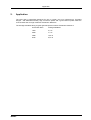
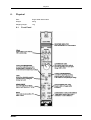
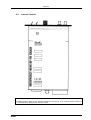
7070 Analog-to-Digital-Converter User Manual copyright FAST ComTec GmbH Grünwalder Weg 28a, D-82041 Oberhaching Germany Version 2.0, July 7, 2005 Software Warranty FAST ComTec warrants proper operation of this software only when used with software and hardware supplied by FAST ComTec. FAST ComTec assumes no responsibility for modifications made to this software by third parties, or for the use or reliability of this software if used with hardware or software not supplied by FAST ComTec. FAST ComTec makes no other warranty, expressed or implied, as to the merchantability or fitness for an intended purpose of this software. Software License You have purchased the license to use this software, not the software itself. Since title to this software remains with FAST ComTec , you may not sell or transfer this software. This license allows you to use this software on only one compatible computer at a time. You must get FAST ComTec's written permission for any exception to this license. Backup Copy This software is protected by German Copyright Law and by International Copyright Treaties. You have FAST ComTec's express permission to make one archival copy of this software for backup protection. You may not otherwise copy this software or any part of it for any other purpose. Copyright 1988 - 2005 FAST ComTec Communication Technology GmbH, D-82041 Oberhaching, Germany. All rights reserved. This manual contains proprietary information; no part of it may be reproduced by any means without prior written permission of FAST ComTec, Grünwalder Weg 28a, D-82041 Oberhaching, Germany. Tel: ++49 89 66518050, FAX: ++49 89 66518040, http://www.fastcomtec.com The information in this manual describes the hardware and the software as accurately as possible, but is subject to change without notice. ComTec GmbH II Table of Contents 1. Introduction .............................................................................................................................. 1-1 2. Application ............................................................................................................................... 2-1 3. Specification............................................................................................................................. 3-1 3.1. Inputs........................................................................................................................... 3-1 3.2. Outputs........................................................................................................................ 3-1 3.3. ADC Signal Timing...................................................................................................... 3-2 3.4. Frontpanel Controls..................................................................................................... 3-2 3.5. Indicators..................................................................................................................... 3-3 4. Performance ............................................................................................................................ 4-1 5. Power Requirements ............................................................................................................... 5-1 6. Physical.................................................................................................................................... 6-1 6.1. Front Panel.................................................................................................................. 6-1 6.2. Rear Panel .................................................................................................................. 6-2 6.3. Internal Controls.......................................................................................................... 6-3 7. Operating Instructions.............................................................................................................. 7-1 7.1. Installation ................................................................................................................... 7-1 7.2. Power-Up .................................................................................................................... 7-1 7.3. Pulse Height Analysis ................................................................................................. 7-1 7.3.1. ADC Setup ..................................................................................................... 7-1 7.3.2. Offset.............................................................................................................. 7-1 7.3.3. ZERO ............................................................................................................. 7-1 7.3.4. LLD Lower Level Discriminator ...................................................................... 7-2 7.3.5. ULD Upper Level Discriminator...................................................................... 7-2 8. Theory of Operation ................................................................................................................. 8-1 8.1. Signal Input Section .................................................................................................... 8-1 8.2. Conversion Sequence................................................................................................. 8-1 ComTec GmbH III Introduction 1. Introduction The 7070 ADC is a high resolution Wilkinson type Analog to Digital converter with 13 bit conversion range. The use of state of the art integrated circuitry provides excellent performance and stability. The 7070 is a single-NIM module. ComTec GmbH 1-1 Application 2. Application The 7070 ADC is specifically designed for use in nuclear -and x-ray spectroscopy. Excellent integral - and differential linearity, high conversion speed and a good channel profile make the 7070 an ideal ADC for high resolution Germanium Detectors. The average deadtime taking a typical gamma-spectrum with a Germanium detector is ComTec GmbH Conversion Gain Average Deadtime 1024 3,7 us 2048 7,1 us 4096 13,9 us 8192 27,4 us 2-1 Specification 3. Specification 3.1. Inputs SIGNAL IN accepts positive or bipolar pulses (positive portion leading) input range 25m V to 10 V, input impedance 1000 ohm. Risetime 100 ns to 100 us, flat top, width 0,5 us minimum, fall time 200 ns to 100 us, DC-coupled, front panel BNC. GATE IN accepts pos. TTL Level or signal. Width 100 ns. Input impedance approx. 4,7 kOhm (pull-up). For coincidence mode of operation - COINCIDENCE/ANTICOINCIDENCE switch has to be in COINC position, Front panel BNC connector. 3.2. Outputs DATA provides 13 bit data output lines and command I/0 Lines - see Rear Panel connector reference, Amphenol 25 pin Connector, Rear Panel. The polarities of the command I/O (handshake) lines are individually selectable via jumpers. The factory settings are: DRDY negative true / active low DACC negative true / active low DEAD positive true / active high ENC positive true / active high DENB negative true / active low The polarity of the data lines is always negative true / active low. IMPORTANT NOTE : The ENC polarity jumper on the board is labeled the wrong way. Thus, an ENC jumper setting of "-" corresponds to "positive true" and vice versa. SCA Rear panel BNC Connector, positive TTL Output, width approx. 1 us. Output pulse appears for every event that corresponds to an input signal with an amplitude that falls between LLD and ULD setting. ComTec GmbH 3-1 Specification 3.3. ADC Signal Timing 3.4. Frontpanel Controls OFFSET Five toggle switches for digital offset, range 256 to 4096. CONVERSION GAIN Six position rotary switch selects full-scale resolution of input signal. For 10 V Input signal 256, 512, 1024, 2048, 4096 or 8192 channels can be selected. Data output is 8 bit to 13 bit corresponding to Conversion Gain switch setting. LLD Screwdriver adjustable 20-turn precision potentiometer to set lower level discriminator, continuously adjustable from +20mV to +10V. ULD Screwdriver adjustable 20-turn precision potentiometer to set upper level discriminator, continuously adjustable from +10V to +20mV. ZERO Screwdriver adjustable 20-turn precision potentiometer to set the analog zero level. Range + 200mV. ComTec GmbH 3-2 Specification COINC /COINC Toggle switch to select Coincidence or Anti coincidence. In PHA mode no signal is required for operation. For Coincidence or Anti coincidence mode of operation TTL input must be present during the linear gate time. Coincidence: positive TTL pulse Anti-coincidence: TTL pulse going to zero 3.5. Indicators DEADTIME LED Bargraph display for deadtime 0% to 100%. ComTec GmbH 3-3 Performance 4. Performance CONVERSION TIME (1,0 + 0,01 N) us - where N is the channel address generated by the 7070 ADC, N is the selected range inclusive of the selected digital offset. ADC DEADTIME Time to peak + Conversion time + Transfer time to MCA. (The 7070 has a one word buffer which normally eliminates the transfer time) LINEARITY Integral Nonlinearity + 0.05 % of full scale over top 99 % of range. Differential Nonlinearity <<+ 1 % of full scale over top 99% of range. STABILITY Gain 50 ppm/degree Celsius Zero 50 µV /degree Celsius COUNT RATE SHIFT ComTec GmbH + 0,5 Channels at rates up to 50 k events/s 4-1 Power Requirements 5. Power Requirements + 24 V 80 mA - 24 V 120 mA +6V 600 mA -6V 20 mA ComTec GmbH 5-1 Physical 6. Physical Size: Single width NIM module Weight: 0.8 kg Shipping weight: 1 kg 6.1. Front Panel ComTec GmbH 6-1 Physical 6.2. Rear Panel ADC port connctor SCA Output BNC type connctor ComTec GmbH 6-2 Physical 6.3. Internal Controls IMPORTANT NOTE : The ENC polarity jumper on the board is labeled the wrong way. Thus, an ENC jumper setting of "-" corresponds to "positive true" and vice versa. ComTec GmbH 6-3 Operating Instructions 7. Operating Instructions 7.1. Installation The 7070 ADC can be used in any NIM-BIN that supplies + 24 V and + 6 V. Ample airflow must be provided for sufficient cooling of the active components of the 7070 ADC. Do not cover bottom or top of NIM-BIN. 7.2. Power-Up Before powering up of the NIM-BIN, connect ADC to MCA, MCD or the supplied cable. computer interface using Connect input signal and then power up the NIM-BIN. Depending on amplitude of input signal and count rate the Deadtime LED-bar-display will be illuminated. NOTE : if LED-bar-display indicates 100 % deadtime even with low countrate, there is most likely a DClevel on your input signal. Adjust the DC adjust on your amplifier to zero DC-offset or AC-couple your input-signal to the ADC signal input. 7.3. Pulse Height Analysis 7.3.1. ADC Setup Set conversion gain to the desired range and view the data in the MCA, MCD or computer. With different conversion gain settings and some adjustment of the external signal amplifier the ADC can be calibrated. 7.3.2. Offset In steps of 256 channels the set energy range can beshifted left relative to the, memory of the MCA, MCD or Computer. Example: ADC set to 8k conversion gain. With no offset (all switches down the memory will accumulate data in channel 0 to 8191. If you now switch the 4k offset switch up the 7070, will accumulate the upper half of the 8k spectrum in channels 0 to 4095 of the memory. This feature is useful as it enables to accumulate an 8k spectrum in a 1k MCA memory by taking 8 successive measurements with different offset settings. 7.3.3. ZERO With the Zero control the Zero point of the ADC can be adjusted to make the input signal amplitude directly proportional to the channel number. This is a useful feature if MCA's are used to accumulate data that do not have an energy calibration feature. It greatly simplifies all manual calculations required to determine the energy of unknown peaks. ComTec GmbH 7-1 Operating Instructions If the 7070 ADC is used with MCD’ s or computers address values can be directly calibrated in energy - an adjustment of the Zero point is therefore not required. 7.3.4. LLD Lower Level Discriminator Can be used to reduce deadtime . The LLD should be set that all input signals having an amplitude less than the first channel of interest are rejected. Setup the LLD visually while accumulating data in your MCA, MCD or computer. Turn the LLD potentiometer clockwise until the channels below the first channel of interest no longer increment. The LLD also determines the lower energy level of the SCA output. 7.3.5. ULD Upper Level Discriminator Can also be used to reduce deadtime. The ULD should be set that all input signals having an amplitude higher than the last channel of interest are rejected. The setup is the same as described for the LLD except that the ULD potentiometer has to be turned counterclockwise. The ULD also determines the upper energy level of the SCA output. NOTE: If the ULD is set below the LLD the ADC will not operate. ComTec GmbH 7-2 Theory of Operation - Conversion Sequence 8. Theory of Operation The Model 7070 ADC is a Wilkinson type Analog-to-Digital Converter with a clock frequency of 100 MHz. 8.1. Signal Input Section The input is connected to a fast peak-detector and a lower threshold comparator. Every event which has an amplitude that passes the lower threshold triggers the Control Logic. The ultra fast peak-detector OP-Amp charges the storage capacitor via three Schottky-diodes. When the maximum amplitude level is reached, the Schottky-diodes go into reversed bias and the OP-Amp output slews very fast to the negative supply. The storage capacitor now holds the peak amplitude value of the in-put signal. At the time the OP-Amp output changes to negative the Control Logic checks if the Lower Level has been crossed but not the Upper Level. If also the Coincidence FF is set, the Control Logic starts the conversion sequence. If above conditions are not met the Control Logic rapidly discharges the storage capacitor and resets the input stage. 8.2. Conversion Sequence At the start of the conversion sequence the input OP-Amp is disabled to prevent further input signals to cause disturbance. After a short delay the Control Logic activates the Synchronization Circuit and starts the linear ramp current-source synchronously with the 100 MHz, clock. During the linear ramp the clock pulses are counted in the fast l3-bit ripple counter - which can have various presets as selected by the digital offset switches. When the linear ramp crosses the zero level (adjustable with the front panel "zero" potentiometer) the conversion stops and halts the counter. If the counter has a value within the selected range (Conversion Gain setting) the value is latched in the output buffer register and the "data ready" FF is set - which signals to the connected MCA, MCD or computer that a valid conversion took place. Data can now be transferred by an external "data accepted" signal, whereby the "data enable" signal must be true to turn the output-buffers on. Either "data accepted", "enable converter" or power on clears the data-ready FF. While data is stored in the output buffer another conversion can take place. ComTec GmbH Appendix 8-1