1
DESIGN AND SIMULATION OF AN MC68000-BASED
MULTIMICROPROCESSOR SYSTEM
James T. Kuehn
Howard Jay Siegel
Peter D. Hallenbeck
Purdue University
School of Electrical Engineering
West Lafayette, IN 47907, USA
C.mmp [22], Cm* [18]).
As with SIMD architectures, there is a multiple data stream and an interconnection network.
A Multiple-SIMD machine is a parallel processing system that can be structured as one or more
independent SIMD machines of varying sizes (e.g.,
MPP C8D). A partitionable SIMD/MIMD machine can
be structured as one or more independent SIMD
and/or MIMD machines of varying sizes (e.g., PASM
[133).
SIMD and MIMD parallelism has been shown to be
applicable to a wide variety of image processing
tasks C13, 14, 15]. In this paper, the SIMD mode
is emphasized; however, the use of full processors
and the overall organization of the system will
also allow MIMD operation.
The system to be
presented could be used as a single SIMD machine,
or
as a building block for a multiple-SIMD
machine, or a partitionable SIMD/MIMD machine (using the techniques described in [13]).
SIMD algorithm simulations for several machine
configurations have been performed [5, 11]. These
studies have examined the possibilities for overlapped operation of the control unit and processors. Overlapping can be improved as additional
hardware (e.g., latches, buffers) is added at the
interfaces of these components.
Each hardware
configuration represents a "case" for which relative run time performance of assembly language
test algorithms was measured.
The results of
these simulations were used as a basis for the
control unit/processor organization described in
this paper. A design based on this organization
and employing currently available off-the-shelf
components is described and simulated.
This design work is motivated by two research
projects at Purdue.
One is the development and
implementation
of
the
PASM
(partitionable
SIMD/MIMD) multimicroprocessor system. The other
is the study of the use of parallel processing for
mapping applications.
In Section II, a model of
the
proposed
SIMD/MIMD system is given. A summary of our earlier SIMD algorithm simulation studies and overlapping schemes is presented in Section III. In
Section IV, the design of a multimicroprocessor
system which incorporates Motorola MC68000 processors is described. The hardware organization of
the control unit, processors, and additional support components is discussed in detail in Section
V.
It is shown that the interface logic for the
microprocessors necessary for SIMD/MIMD processing
will be minimal; thus the high cost of a custom
VLSI design can be saved. Ideas for a prototype
patterned on this design are given. Finally,
results of simulation studies of the proposed
MC68000-based machine are summarized in Section
VI.
Abstract — The design of a multimicroprocessor
system for image processing and pattern recognition applications utilizing the 16-bit Motorola
MC68000 and other off-the-shelf components is
described. This system can be dynamically reconfigured to operate in either SIMD or MIMD mode and
can be used as a building block for the PASM partitionable SIMD/MIMD machine.
The results of
simulations of SIMD operation that were used to
guide the design of the MC68000-based system are
discussed.
The possibilities
for
overlapped
operation of the SIMD control unit and processors
are examined. The system architecture, including
hardware to interface the off-the-shelf components
needed for SIMD/MIMD processing, is given. Finally, simulation studies of the performance of the
proposed MC68000-based system are presented.
I.
Introduction
The demand for higher throughput and very large
database handling capabilities is forcing computer
system designers to consider nontraditional architectures, notably distributed/parallel systems.
Architects have
proposed
microprocessor-based
large-scale parallel processing systems with as
many as 2
and 2
processors [e.g., 9, 173 that
show promise in meeting these data-handling and
throughput demands.
Two types of parallel processing systems are
SIMD and MIMD C4D.
SIMD (single instruction
stream - multiple data stream) machines (e.g., Illiac IV [33, STARAN [13) typically consist of a
set of N processors, N memories, an interconnection network, and a control unit. The control
unit broadcasts instructions to the processors,
and all enabled ("turned on") processors execute
the same instruction at the same time. Each processor executes instructions using data from a
memory with which only it is associated. The interconnection network allows interprocessor communication.
An MIMD (multiple instruction stream - multiple
data stream) machine also typically consists of N
processors and N memories, but each processor can
follow an independent instruction stream (e.g.,
This research was supported by the Air Force Office of Scientific Research, Air Force Systems
Command, USAF, under Grant No. AFOSR-78-3581, and
by the Defense Mapping Agency, monitored by the
United States Air Force Systems Command, Rome Air
Development
Center,
under
Contract
No.
F30602-81-C-0193. The United States Government is
authorized to reproduce and distribute reprints
for Governmental purposes notwithstanding
any
copyright notation hereon.
353
II.. Model of the Proposed SIMD/MIMD System
structions and generates no network conflicts
while disabled.
The basic system components of the proposed
machine are a Control Unit (CU) (including its own
The interconnection network has the single task
of transferring data among the PEs. It accepts
data from the "source" PEs at its N input ports
and routes the data to its N output ports, where
it is accessible to the "destination" PEs.
The
Generalized Cube network, a network being considered for use in PASM for reasons discussed in
[12], is assumed in the simulations. This network
consists of n stages of switches and is controlled
by routing tags.
In a serial processor, components 4, 5, 6, 9,
10, and 11 are either unnecessary or are meaningless. These functions comprise what is known as
the "overhead due to parallelism." Well-designed
CU/PE and PE/network interfaces can minimize this
overhead by overlapping the operations of the CU,
PEs, and network. Overlapping allows the CU, the
set of PEs, and the network to perform their own
tasks, synchronizing only when there is some information to be exchanged. Examples of overlapping are:
(1) the CU fetching the next instruction in the
stream or executing CU instructions while the
PEs are executing an instruction,
(2) the PEs executing an instruction while a set
of data items is passing through the network,
and
(3) the network passing more than one set of data
items from input to output simultaneously.
In this paper, (1) is analyzed and simulated.
(Aspects of (2) and (3) are discussed in [113, but
are beyond the scope of this paper.)
In SIMD mode, all of the enabled PEs will execute instructions broadcast to them by the CU. A
masking scheme is a method for determining which
PEs will be active at a given point in time. An
SIMD machine may have several different masking
schemes.
The general masking scheme uses an N-bit PE enable vector to determine which PEs to activate.
PE i will be active if the i-th bit of the PE enable vector is a 1, for O<i<N. A mask instruction
is executed whenever a change in the active status
of the PEs is required. The Illiac IV, which has
64 processors and 64-bit words, uses general masks
[16].
However, when N is larger, say 1024, a
scheme such as this becomes less appealing.
The PE address masking scheme [10] uses a 2nbit mask to specify which of the N PEs are to be
activated. PE address masks are fetched from the
instruction stream and sent to the masking operations unit to be decoded into a PE enable vector
[13].
This vector is passed to the CU/PE interface to effect the change in status of the PEs.
General masks are passed to the CU/PE interface
unchanged by the masking operations unit.
PE address masks may be decoded and then manipulated by the masking operations unit. For example, decoding two PE address masks, "or"-ing them
together, and using the result as the PE enable
vector activates the union of the sets of PEs activated by each individual mask [13]. This implies that the masking operations unit can perform
basic boolean operations on masks and can temporarily store a number of general and decoded PE
address masks.
memory), N=2 n processors, N memory modules, and an
interconnection network.
The processors are microprocessors that perform the actual SIMD and
MIMD computations.
A memory module is connected
to each processor to form a processor/memory pair,
called a processing element (PE). The PEs are
numbered (addressed) from 0 to N-1. The interconnection network provides a means of communication
among the PEs.
In SIMD mode, the CU fetches instructions from
its memory, executes the control flow instructions
(e.g., branches), and broadcasts the data processing instructions to the PEs. The CU may coordinate the activities of the PEs in MIMD mode.
"Functional-block" models of the interactions
of the CU, PEs, and network will now be presented.
Later, the hardware used to implement each function will be described.
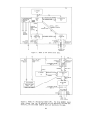
The CU's functions may be classified into six
areas
(consult
Figure
1 ) . The numbers in
parentheses in Figure 1 correspond to the component classifications given below.
(1) The CU execution unit performs program flow
operations (e.g., loop counting, branching).
(2) CU memory contains the SIMD
instruction
stream.
It also provides data storage for
the CU execution unit.
(3) The fetch unit fetches instructions from CU
memory and routes them to the CU execution
unit, the PEs (via the CU/PE interface), or
to other specialized CU hardware.
(4) The CU/PE interface collects PE instructions
and enable signals and broadcasts these to
the PEs.
(5) The masking operations unit decodes and manipulates masks.
Masks specify which PEs are
to be enabled or disabled.
(6) Microprogrammed logic directs the operations
of the fetch unit, masking operations unit,
and other specialized CU hardware.
Signals
are generated for system control functions
(e.g., "bringing up" the CU and PE execution
units, initializing I/O devices).
A PE's functions include the following (consult
Figure 2 ) .
(7) In SIMD mode, the PE execution unit accepts
instructions broadcast by the CU and performs
computations that process the local
(PE
memory) data stream. In MIMD mode, instructions and data are fetched from PE memory.
(8) PE memory contains data for the SIMD mode
operations of the PE execution unit. It also
contains instructions and data for MIMD mode
operations.
(9) The PE/network interface sends data and routing information to and accepts data from the
interconnection network.
(10) The condition codes register stores the PE
execution unit condition codes.
The data
condition select lines specify which bit or
boolean function of bits in the register will
represent the status of the PE.
(11) Logic controlled by the PE's enable/disable
signal ensures that the PE executes no in354
Figure 1. Model of the Control Unit (CU).
Figure 2. Model of a Processing Element (PE). The three ADDRESS buses
shown coming from the PE execution unit are physically the same bus.
Similarly, the three READ (/WRITE) buses are physically the same.
The Illiac IV and MPP control units and PEPE
arithmetic control unit use the case 3 overlap
processing method [2, 19, 213. All three machines
employ data conditional masking, but the resulting
masks are stored in the PEs themselves.
For case 4, a CU instruction buffer is added to
the case 3 configuration. An implicit assumption
for this case is that the fetch unit and CU execution unit are independent processors. (For cases
1-3, the fetch and execution units are not necessarily distinct.) The fetch unit classifies instructions as CU or PE instructions and sends them
to the appropriate instruction buffer. The fetch
unit must distinguish branch operations (including
"if any/if all" branches) by stopping the fetching
process when these instructions are encountered.
Branch instructions affect the program counter
(which the fetch unit maintains to know the "next"
instruction), so the fetch unit must wait until
the CU has emptied its instruction buffer and adjusted the program counter based on the result of
the branch before continuing. Fetching is also
discontinued during masking operations to allow
the masking operations unit to associate the new
PE enable signals with subsequently fetched PE instructions.
For the previous cases, the fetch unit decoded
each instruction in order to determine where (the
CU or the PEs) the instruction would be executed
and the size (number of operands) of the instruction. This scheme required that the fetch unit
have full knowledge of CU and PE instruction types
and formats. This adds considerable complexity to
the fetch unit, and would necessitate changes to
it if either the CU or PE execution units were
changed. An effective solution is to associate a
tag with each CU memory word, specifying which
component (CU execution unit, CU microprogrammed
logic, or PEs) is to interpret the word. Cases 5
and 6 correspond to cases 3 and 4, but with fetching and buffering by words rather than by instructions. Each word (as opposed to each instruction,
including both opcode and operands, as in cases
1-4) sent to the PE instruction buffer will have
associated with it an N-bit enable vector.
The tag scheme just described has several advantages. First, the PEs will only be idled when
the instruction queue becomes empty; an unlikely
event since the instructions are delivered to the
queue at the rate of the CU memory access time.
The time needed to decode the tag is negligible in
comparison to the time necessary to fully decode
each instruction and determine how many operand
words are associated with that instruction. The
fetch unit no longer requires knowledge of the
specifics of the PE instruction set since PE instruction words are treated as data. Furthermore,
a 16-bit line connecting the CU to the processors
is needed, as opposed to the 80 bit line if complete instructions, including operands, were sent
to the PEs (assuming MC68000 instructions require
1 to 5 16-bit words). However, the instruction
opcode must be decoded by the PE execution units
to determine if "immediate" data operands or address fields are present. This step was previously done by the control unit; data operands were
associated with the instruction opcode before being broadcast to the PEs.
Data conditional masks are the result of performing a test on local (PE) data in an SIMD
machine environment,
where the results of different PEs1 evaluations may differ. As shown in
Figure 1, the CU receives an N-bit data conditional mask comprised of N one-bit "true/false" data
conditional results, one result from each PE's
condition code register. The "true/false" data
conditional results are stored in the masking
operations unit for use in activating or deactivating the PEs. For example, this type of data
conditional masking was used in PEPE to implement
the "where" conditional tests [213.
Certain CU execution unit instructions cause a
branch based on data conditional mask information.
For example, "if any" PE meets some criteria (a
bit in the data conditional mask is "true"), the
CU execution unit would execute a branch to a different part of the program. The masking operations unit uses the data conditional mask results
from the PEs to evaluate the "if any," "if all,"
etc., conditions.
III.
A.
SIMD Simulation Overview
Introduction
Our earlier SIMD algorithm simulation studies
have examined the possibilities for overlapped
operation of the control unit, processors, and interconnection network [5, 11]. Overlapping can be
improved as additional hardware (e.g., Latches,
buffers) is added to the CU/PE and PE/network interfaces. Six hardware configuration "cases" were
identified and the relative run time performance
of assembly language test algorithms was measured
for each. A summary of the four cases from C53
and the two cases using tagged instruction words
from [113 appear in Subsection B. In Subsection
C, simulation results from the six cases will be
summarized and compared. Based on the results,
one of the cases will be chosen
for the
MC68000-based design.
B. Summary of Cases
In case 1, the CU and PEs are forced to operate
in lock-step fashion. That is, while the CU is
fetching or executing an instruction, the PEs are
idled, and vice-versa. The STARAN system operates
in a case 1 mode since there is a single instruction register in the control unit which contains
the currently executing instruction C193.
Case 2 allows the CU to fetch instructions or
execute CU instructions while the PEs are executing. However, the CU must wait until the PEs have
completed their operation before broadcasting the
next PE instruction.
A FIFO instruction queue shared by the PEs is
added in case 3. This allows the CU to send PE
instructions (opcodes and operands) to the queue
without having to wait for the PEs to complete
their current instruction. Associated with each
opcode/operand
pair in the queue, the N-bit
enabled/disabled status associated with that instruction (the PE enable vector at fetch time) is
stored. The PE enable vector must be stored since
CU
masking
operations
(changing
the PE
enabled/disabled status) might be performed before
the queued PE instruction is actually executed.
356
C.
Simulation Results
During simulations performed for several assembly language test algorithms, the relative run
time performance of the 6 cases was measured. The
results of cases 1-4 were presented in C5] but are
summarized here for comparison with cases 5 and 6.
The assembly Language instruction set that was
used for the simulations is of our own design. It
is similar to instruction sets supported by sophisticated current microprocessors, but augmented
by instructions for the control unit operations,
masking operations, and network data transfers.
The test algorithms are two versions of an image smoothing algorithm for a 16-PE system smoothing a 16x16 pixel image [13].
For these algorithms, each PE contains a subimage of 4x4 pixels.
In the "original" version of the algorithm, a PE's
subimage pixels and "border" pixels from adjacent
PEs are copied to a 6x6 pixel "work area" array.
Smoothing operations are performed on the pixels
in the work area. For the "improved" version of
the algorithm, the "border" pixels and a subset of
the subimage pixels are copied to the work area.
In this version, both the work area array and the
subimage array are accessed during the smoothing
operations.
As will be shown, the original algorithm performs better for small images, while the
improved algorithm performs better for large (more
realistically-sized) images. Some parameters of
the algorithms are shown in Table 1.
Table 1. Test algorithm characteristics.
The
"TOTAL CU" and "TOTAL PE" columns indicate the
percentages of CU and PE instructions executed.
"CU IF ANY" is a subclass of "CU BRANCH," which is
a subclass of "CU TOTAL." Similarly, "PE NETWORK"
instructions are included in the "TOTAL PE" classification.
Each test algorithm was assembled using a special assembler supporting the augmented instruction set and simulated using our Purdue SIMD Simulation and Timing (PSST) system. An instruction
execution trace for each simulated algorithm was
generated to be used later as input to the timing
algorithms. A small number of PEs and small image
sizes were used since the simulations of the SIMD
system are performed comparatively slowly on a
Table 2.
serial host computer. Details of the algorithms,
instruction set, assembler, simulations, and timing routines are presented in [11].
In preparation for timing the simulations, each
instruction in the instruction set was classified
by its constituent operations and characteristics.
These
characteristics
include the number of
operand words to be fetched, the CU execution time
(for CU instructions), the CU to PE transfer time
(for PE instructions), the PE execution time and
network execution time (for PE instructions),
flags to indicate data conditional mask instructions, branch instructions, network instructions,
and so on. A table of instructions and their
characteristics was prepared.
The timing algorithms reference the instruction
set characterization table and accept input of
relevant timing information (e.g., opcode load
time (1 cycle), 16-bit operand load time (1 cycle), buffer enqueue or dequeue time (1/2 cycle),
mask decoding time (1 cycle)). The interconnection network set-up time and network propagation
delay time were 1 cycle each. Finally, the instruction trace output from the test algorithms
was used as input to evaluate the timing for cases
1-6. Note that the same instruction execution
trace can be used repeatedly for many combinations
of cases and timing assumptions. For these simulations, a circuit-switched network whose ports
are directly connected to PE execution unit registers was assumed. No PE/network overlap was considered.
The run time results shown in Table 2 are nor—
malized such that the case 1 timing = 1.00. As
shown, the run time of case 3 is significantly
less than those of case 2 and case 1. This was
expected since the instruction "mix" for these algorithms is such that PE instructions greatly outnumber CU instructions and PE instructions occur
in large groups, allowing the buffer to do its intended function. The case 4 run time falls somewhere between the case 2 and case 3 timing. The
fact that case 4 performs worse than case 3 for
these algorithms is not surprising since CU instructions rarely occur in groups (thus underutilizing the CU instruction buffer). Further,
the percentage of branch instructions performed
ranges from 70 to 80 percent of the CU instructions, thus preventing the filling of the CU instruction buffer in the case 4 configuration.
In cases 5 and 6 (fetching and buffering by
words), the time needed to fetch and enqueue instructions, including their operands, is proportional to their length (cases 1-4 had a constant
time). However, the simplified tag decoding for
these cases might offset the overhead of the extra
enqueue/dequeue operations.
Comparisons
made
between cases 1-4 and 5-6 may be influenced
Normalized run times for cases 1-6.
The MC68000 is a state-of-the-art 16-bit microprocessor [20, 73. Internally, it can operate
on bit, byte, word (16-bit), and long (32-bit)
data formats.
Its fast cycle time and large address space (currently 24-bit addresses) make it
ideal for image processing applications where
speed and large data set handling capabilities are
a must.
Its very regular instruction set, many
addressing modes, and suitability to high-level
language operations make it easy to program.
While some of the MC68000's functions go unused
when it operates in SIMD mode (e.g., branch and
control operations), these functions are essential
for MIMD "stand-alone" processing.
While the
MC68000 is not quite as "powerful" as the Illiac
IV [33 or PEPE [213 PE, it is considerably more
complex than the STARAN [13 or MPP [23 processors.
Each PE will be able to address any of three
logical address spaces.
Physical PE memory addresses (both ROM and
RAM
addresses)
will
represent one space. Addresses of I/O ports will
be contained in the second space. The PE instruction queue (for the case 5 configuration) will
have addresses in the third space. Initially, all
PEs will be enabled, and have their internal program counter set to the address of the beginning
of the PE instruction queue space. When the PEs
try to fetch the first SIMD instruction, the address sent out by each of the PE execution units
will be decoded by the "address decoding logic" as
a reference to the PE instruction queue space.
This logic will send an "instruction request signal" to the FIFO instruction queue. When all PEs
request an instruction, the buffer acknowledges
the requests and puts an instruction word on all
the PE data buses. Each PE decodes the instruction and performs the operation or requests additional operand words.
If the logic determines
that a PE memory or I/O device address is being
referenced, the operation is performed normally.
strongly by the simpler (and potentially faster)
case 5-6 hardware. For example, enqueue and dequeue times may be shorter for cases 5 and 6 since
all queuing functions involve a shorter, fixedsize word. The very wide bus assumed in cases 1-4
may in reality be a smaller, time-multiplexed bus,
thus increasing the CU/PE instruction transfer
time for those cases. If the fetch, decode, enqueue, dequeue, and execution times are assumed to
be the same as for cases 1-4, cases 5 and 6 perform somewhat worse than the case 2 configuration
because of the aforementioned factors. Case 3 is
faster than case 5 because enqueuing and dequeuing
operations are not done word-by-word. The speed
advantage of case 3 would be negated if it used a
16-bit time-multiplexed bus and a slightly slower
fetch/decode unit. The percentage of instructions
with operands and the average operand length (both
algorithm-dependent parameters) also influence the
relative performance of the cases greatly.
The instruction queue sizes chosen for the case
3-6 configurations also have an effect on the algorithms' run time. The minimum size needed was
seven words for case 3, six for case 4, and three
for cases 5 and 6. A detailed analysis of the
minimum PE instruction buffer sizes required to
get the same overall execution time the infinite
buffer (assumed in Table 2) would provide is given
in C113.
Based on the simulation results obtained for
the SIMD mode, the case 5 configuration has been
chosen. Case 3 was not chosen because of the more
complex fetch unit design and the very wide CU/PE
bus width requirement. Assuming the use of standard microprocessors, the case 3 configuration unnecessarily duplicates the instruction decoding
function of the PEs. A narrower, time-multiplexed
CU/PE bus could be implemented with case 3, but
this approach would likely negate the speed advantage gained by buffering instructions as a unit.
Furthermore, standard microprocessors accept instructions word-by-word. Case 5 simplifies the
design of the fetch unit considerably since tags
associated with each memory word indicate that
word's destination.
The fetch unit requires no
knowledge of either the CU or PE execution unit's
processor instruction set.
The tagged memory
scheme also allows the instruction complement of
the microprogrammed hardware to be developed independently. The PE instruction queue and bus
width of 16 bits is quite manageable. The case 5
queue may be longer since it is word-by-word, but
has a much narrower width that is always fully
utilized. Simulation results of the MC68000-based
system are presented in a later section.
IV.
In SIMD mode, the PE program counter serves
only to identify a request for an instruction
word. The actual value of the PE program counter
is irrelevant, as long as it references an instruction in the PE instruction queue space. However, the program counter is incremented automatically upon receiving an instruction from the PE
instruction
queue.
Eventually,
the program
counter will near the end of the instruction queue
space and will need to be reset. The instruction
queue address space is made large so that the
overhead of resetting the program counter is
minimal.
When the PE enable vector specifies that a PE
is to be disabled, the address decoding logic in
that PE continues to send an instruction request
signal to the PE instruction queue. However, the
acknowledgement and data word from the queue is
intercepted by the logic so that the PE execution
unit never "sees" the instruction.
When the PE
execution unit is re-enabled, processing can continue.
In order to avoid internal modifications to the
PE execution unit, PEs will communicate via the
interconnection network using a sequence of I/O
port read and write operations. A PE specifies
where its data is to be routed by computing the
address of the destination processor (PEs are addressed 0 to N-1). The address is written to an
The MC68000-Based PE
Referring to the model of a PE (Figure 2 ) , consider incorporating the Motorola MC68000 processor
as the PE execution unit. The processor itself,
256K-bytes of PE memory, and some simple latches
(PE/network interface, condition code register)
and logic can easily fit on a single physical
board. The organization of the model was chosen
carefully so that the number of wires running
between the CU and PEs is minimized. The consolidation of specialized hardware in the CU makes
each PE board simpler and cheaper to construct.
358
external (n+1)-bit "network set" Latch (the "exThis action
tra" bit will be described later).
instructs the network to set switches to make a
connection with the destination address [63. Data
transmissions will occur through two 16-bit external data latches called Data Transfer Registers
(DTRs) [133.
One latch is connected to the network input (DTRin), and the other to the network
output (DTRout).
The data to be transmitted is
written to the DTRin latch.
Finally, a control
word is written to an external 1-bit "network
transfer" register, signaling to the network that
the transfer should be made. Subsequent transfers
route items to the same destination until the
"network set" latch is modified. In SIMD mode,
all PEs do these operations at the same time.
In
MIMD mode, PEs use the network asynchronously.
At the destination PE, the network sets a flag
indicating
that
the
DTRout contains newlytransferred data and may be read. When the PE attempts to read DTRout, specialized logic examines
this flag. If the PE attempts to read DTRout
prematurely (the flag is not yet set), the PE is
made to wait until the network has passed the data.
For this reason, other processing is often
done during network transfers to maximize overlapped operation of the PEs and network. In MIMD
mode, a PE might send data faster than the destination PE requires it as input. In this situation, the network-generated signal flag might be
used to interrupt the receiving PE and instruct it
to buffer the incoming data.
When a PE is disabled, logic insures that the
"network set" data does not create "conflicts" in
the network switch settings. The "extra" bit in
the "network set" latch is used to indicate that
this network input should be ignored. A disabled
PE may receive data normally since the DTRout is
unaffected by the enabled/disabled status of the
PE execution unit.
When re-enabled, the PE can
read DTRout.
When a data conditional mask is needed, PE instructions to evaluate the PE data condition are
executed. Then the PEs write their status register (which contains the processor condition codes)
to the condition codes register. Logic associated
with the condition codes register can generate
eight different conditional tests (e.g., equal,
not equal, positive, overflow). Data condition
select lines from the CU specify which of the conditional tests is to be returned to the masking
operations unit as that PE's component of the data
conditional mask.
From time to time, the CU fetch unit will enqueue a JUMP instruction to the beginning of the
PE instruction queue space. This is to prevent
the PE program counters from entering a different
address space. The mechanism that the fetch unit
uses to perform this function will be described
later. When the machine is to change from SIMD to
MIMD mode, the fetch unit broadcasts a JUMP instruction to some address within the PE memory
space.
Typically, this would be the beginning of
a program stored in ROM that would initialize the
PE operating system for MIMD processing. While in
MIMD mode, PEs do not access the PE instruction
queue space since MIMD instructions and data are
contained entirely within the PE memory. When the
PE is ready to revert to SIMD mode, it jumps to
the beginning of the PE instruction queue space.
When all the PEs have done this, SIMD processing
continues.
V.
CU
Architecture Details
There exist no off-the-shelf processors that
can perform all of the functions of the control
unit at a speed sufficient to keep the PE execution units busy. Therefore, fast microprogrammable bit-slice components will be used for all of
the CU specialized functions. These functions include the operations of the fetch unit, masking
operations unit, and CU/PE interface. In order to
simplify the programming of the system and to make
data formats uniform throughout, the CU execution
unit will also be an MC68000 processor. For comparison, the execution component of the Illiac
control unit is a powerful 64-bit integer/floating
point processor [33. The MPP "main control" and
the PEPE arithmetic control unit are also quite
sophisticated [21, 23.
By contrast, the STARAN
execution unit and MPP "PE control" unit consist
of only a few dedicated registers for loop counting and handling of "associative array field
pointers" [19, 23.
The speed at which the bit-slice fetch unit can
fill the PE instruction queue to capacity, and the
Large ratio of PE to CU instructions in algorithms
programmed so far indicates that the MC68000 will
be an acceptable CU execution unit. When the subset of MC68000 instructions actually used in normal CU execution unit operations is
defined
through actual use and further simulation, and if
there is a need for more speed, the MC68000 could
be replaced with a bit-slice machine.
CU memory will be comprised of 20-bit words.
The most significant four bits will be interpreted
by the microprogrammed logic portion of the fetch
unit as a destination for the remaining 16.
The CU fetch unit will contain two registers:
the Fetch Unit Program Counter (FUPC) and the PE
Space Counter (PESC. The FUPC gives the address
of the next instruction to be fetched from CU
memory. The CU execution unit program counter
serves only to identify a request for an instruction word. The actual value of the CU execution
unit program counter is irrelevant, except when
branch instructions are executed.
The FUPC and
the CU execution unit program counters must be
equal before a branch instruction is executed
since computations using the program counter will
be done (e.g., relative branches).
The PESC begins at zero and is incremented each
time a word is enqueued in the PE instruction
queue. When the PESC reaches a threshold value
close to the size of the PE instruction queue
space, the fetch unit enqueues a JUMP instruction
before the next PE instruction. (The first word
of a PE instruction has a special tag.) The JUMP
instruction causes the PE program counter to be
reset to the beginning of the PE instruction queue
space (see Section IV). When the JUMP instruction
is enqueued, all PEs are temporarily enabled. The
PESC register is also reset to zero.
The 4-bit memory word tags will specify what
sequence of actions the microprogrammed Logic is
to take. Examples of these actions are enqueuing
a PE instruction opcode or operand, sending a CU
359
The large address space of the MC68000 could be
used to access any part of up to thirty-two 256Kbyte PE memories if the hardware is so arranged.
This scheme would be most useful in a prototype:
the CU execution unit could load and unload PE
memories, monitor the behavior of individual PEs,
and so on. (A real system would not use this
scheme because of speed and memory contention
problems.)
VI. MC68000 Simulation Results
instruction to the CU execution unit, mask decoding, and-ing and or—ing of masks, PE data condition selection, initialization of the CU execution
unit, masking operations unit, PEs, or I/O devices, etc.
The CU fetch unit never operates at the same
time the CU execution unit is performing branch
instructions or while the masking operations unit
is operating. The CU execution unit may modify
the program counter which the fetch unit maintains
to know the "next" instruction. The masking
operations unit may modify the PE enable vector
which must be associated with each enqueued PE instruction.
The masking operations unit maintains a stack
of N-bit masks generated by nested "where" conditionals and PE address masks [113. The PE enable
vector that is currently on the top of the stack
is enqueued whenever a PE instruction word is enqueued. The details of the stack operations,
stack hardware, and the interplay between SIMD
programs and masks are discussed in [113.
The PE instruction queue (CU/PE interface) is a
high-speed I/O buffer N+16 bits wide and 32 words
long. This length allows about ten average PE instructions to be queued. A head and tail pointer
indicate the position of the next word to be dequeued or enqueued, respectively. The buffer dequeues a word if nonempty and when all PEs make
the request (inactive PEs are always "requesting"). The fetch unit may enqueue a word provided
the queue is nonfull.
In order for the instruction queue to be useful, the total time to fetch an average instruction, decode its tags, and enqueue its constituent
words should not exceed the time needed by the PE
to execute
that
instruction.
Given
that
2900-series microprogrammable bit-slice components
have a cycle time of 200 nanoseconds vs. the
MC68000
basic
memory
cycle time of 500
nanoseconds, there should be no problem in filling
the PE instruction queue to keep the PEs "satisfied." If the queue is sufficiently large, the execution of several consecutive CU execution unit,
masking, or control instructions should not empty
the queue and "starve" the PEs.
For a prototype system of size N = 16 or 32
PEs, the MC68000 execution unit could be used to
simulate some of the CU operations in software and
monitor the PEs. For example, the masking operations unit and CU/PE interface could be implemented in software (but at a cost in system speed).
The simulation of the MC68000-based system was
carried out using the same techniques as described
earlier. However, these simulations required the
writing of new SIMD algorithms in the MC68000 instruction set, a specialized version of an MC68000
assembler, and new PSST simulation programs. The
PSST timing algorithms were largely unchanged, but
a new table of instruction timing characteristics
had to be prepared.
The PSST simulator consists of two main
coroutines: the simulation of an MC68000 processor
and the simulation of the CU microprogrammed logic. The actions of the fetch unit and masking
operations unit are included in the CU microprogrammed logic simulation. When the CU execution
unit is to be activated, a copy of the "CU data
area" is passed to the MC68000 simulator and processing is initiated. When a PE is to be activated, a copy of the appropriate "PE data area" is
passed to the MC68000 simulator. The action of
the CU/PE interface (case 5: overlapping of the
instructions) is simulated by the timing routines.
The PSST simulator for the MC68000 system is
largely complete although it lacks BCD arithmetic
operations, trap and exception processing, interrupts, and MIMD operation (the asynchronous interaction of the PEs). It also cannot detect interconnection network "conflicts." Major effort
will be required to implement interrupts and MIMD
operation
in both the simulation and timing
routines.
Two versions of the SIMD image smoothing algorithm for a 16-PE system were simulated. The algorithms are identical to those described in Section III. Simulations of both algorithms were
performed for a variety of image sizes ranging
from 16x16 to 128x128 pixels. The complete image
can be superimposed onto an array of 4x4 (=16) PEs
such that each PE processes a subimage of 4x4 to
32x32 pixels.
Table 3 compares the simulation and timing
Table 3. Comparison of smoothing algorithm simulation and timing
characteristics. The "original" algorithm run time results are normalized to 1.00. The internal cycle time is 250ns. All of the simulations
are performed with N=16 PEs.
360
If better run times were necessary, the algorithm
could be restructured to smooth a window of eight
nearest-neighbor pixels (as opposed to nine) and
scale the data by shifting the result right by
three bits. A typical 3-bit shift requires 7 cycles, or about 10% of the divide cycle time. However, a load and add cycle (about 7 cycles) is
saved since only eight pixels are used in the window. Thus a 35% improvement can be gained by replacing the divide instruction.
The 75 cycles for a divide instruction is the
maximum instruction time; the actual time required
is data-dependent and is not considered by the
PSST timing routines. If some PEs finish the instruction before others, they will be made to wait
until all the PEs have finished. Recall that a PE
instruction is dequeued from the FIFO buffer only
when all PEs make the request for the next instruction. However, if all of the PEs finish the
division before the 75 cycle maximum, the hardware
will be able to exploit this and release the next
instruction to the PEs.
The simulation results presented may be extrapolated to determine timings and speedups for other machine and/or image sizes. The run time of an
algorithm depends on the relative sizes of the
machine and the image, or equivalently, the subimage size in pixels per PE. For the smoothing examples, a minimum machine size of 4 PEs is necessary and sufficient so that all relevant inter-PE
transfer and masking instructions are included.
For example, a 4-PE SIMD machine can smooth an 8x8
pixel image in the same amount of time as a 16-PE
machine can smooth a 16x16 pixel image. In each
case, a PE operates on a subimage of 16 pixels.
Similarly,
since
16 PEs can smooth a
128x128 (=16K) pixel image in 31ms, a 64-PE system
of the same design and using the same algorithm
could smooth a 256x256 (=64K) pixel image in 31ms.
(For larger machines, the number of stages in the
Generalized Cube network will increase; however,
assuming that the propagation delay of the network
is overlapped with PE operations, the impact of
the added stages is negligible.) In general, increasing the number of PEs by a factor of four allows four times as many pixels to be processed in
the same amount of time. However, this does not
mean that processing four times as many pixels
will take four times as long for a fixed machine
size. In the latter case, the fixed and variable
costs of performing the particular algorithm must
be taken into account.
results for the two smoothing algorithms. The run
time has been normalized such that the original
algorithm run time=1.00. These results indicate
that the original algorithm is more efficient for
small subimages (fewer than 12x12 pixels per PE)
than the "improved" algorithm. The improved algorithm would be used for real-world-size problems.
The actual algorithm execution time can be calculated for a given algorithm/image size pair by
multiplying the number of cycles by the cycle
time. Assuming a standard 8HHz MC68000 processor,
the internal cycle tine is two clock cycle times,
or 250ns. Thus, a 128x128 (=16K) pixel image can
be smoothed by the 16-PE system in about 31ms.
Note that this is algorithm execution time. The
simulations do not include data load/unload time
between primary and secondary memory (which will
be highly implementation dependent, e.g., see
C13D).
The 128x128 pixel simulation required about 16
minutes of VAX cpu time. This corresponds to an
average execution rate of over 19 SIMD instruction
per second of cpu time. Recall that the simulator
executes a single PE instruction 16 times, once
for each PE. Somewhat less than half of the cpu
time may be saved if the "PE memory dump" following the simulation is inhibited. The writing of
128 numbers to disk files (for verification of
the smoothed output) takes a considerable amount
of time.
A "serialized" (single PE) algorithm was constructed from the original parallel algorithm to
determine the "speedup." The serial algorithm
operates on the entire image (rather than a subimage) and thus does not need to perform masking or
inter-PE transfer operations. When the number of
masking and transfer operations per pixel processed (parallel overhead) is high, the parallel
algorithm will not be very efficient. If no over—
head is involved, the parallel algorithm should
execute 16 times faster on a 16-PE machine than on
a 1-PE machine. As shown in Table 4, the parallel
algorithm performs relatively poorly for small subimage sizes, but approaches a perfect speedup for
"real-size" tasks.
Table 4. Determination of the speedup factor of
the original parallel algorithm. All of the simulations are performed with N=16 PEs.
VII.
Conclusions
Based on the results of past simulation studies, the design of an extensible SIMD/MIMD
machine based on state-of-the-art microprocessors
and off-the-shelf components was developed. The
interface logic necessary for SIMD/MIMD processing
was found to be minimal. Thus the high cost of
designing and fabricating a custom VLSI PE has
been saved. The architecture could be used as a
single SIMD/MIMD machine, or as a building block
for a larger multiple-SIMD or partitionable
SIMD/MIMD system using the techniques described in
C13D. Also, the design presented is easily modified even after it is constructed since the CU
does not decode any PE instructions. This is
It was observed that the MC68000 divide instruction, which is executed once per pixel processed to scale the result, accounts for roughly
35% of the total run time. The divide instruction
requires about 75 machine cycles as compared to a
typical add instruction requiring about 4 cycles.
361
[11] H. J. Siegel and J. T. Kuehn, Parallel Image
Processing/Feature Extraction Algorithms and
Architecture Emulation: Interim Report for
Fiscal
1981, Volume
II: Architecture
Emulation, School of Electrical Engineering,
Purdue University, Technical Report, Oct.
1981.
[12] H. J. Siegel and R. J. McMillen, "The multistage cube: a versatile interconnection
network," Computer, Vol. 14, Dec. 1981, pp.
65-76.
[13] H. J. Siegel, L. J. Siegel, F. C. Kemmerer,
P. T. Mueller, Jr., H. E. Smalley, Jr., and
S. D. Smith, "PASM: a partitionable
SIMD/MIMD system for image processing and
pattern recognition," IEEE Trans. Comp.,
Vol. C-30, Dec. 1981, pp.934-947.
[14] L. J. Siegel, "Image processing on a partitionable SIMD machine," in Languages and
Architectures for Image Processing, M. Duff
and S. Levialdi, ed.. Academic Press, London, 1981.
[15] L. J. Siegel, E. J. Delp, T. N. Mudge, and
H. J. Siegel, "Block truncation coding on
PASM," 19th Ann. Allerton
Conf. on
Communication, Control, and Computing, Oct.
1981, pp. 891-900";
[16] K. G. Stevens, Jr., "CFD - A FORTRAN-like
language for the Illiac
IV," Conf.
Programming Languages and Compilers
for
Parallel and Vector Machines, ACM, Mar.
1975, pp. 72-76.
[17] H. Sullivan, T. R. Bashkow, and K. Klappholz, "A Large-scale homogeneous, fully
distributed parallel machine," 4th Symp.
Comp. Arch., Mar. 1977, pp. 105-124.
especially important since the MC68000 processor
is not yet in the final stages of its evolution.
The use of an MC68000-based control unit in a prototype has also been shown to be highly desirable.
In a final design however, many of the CU functions will have to be implemented using bit-slice
technologies.
Given these considerations, it appears that a
powerful SIMD/MIMD system having at least 128 processors could be built without encountering severe
physical
hardware
restrictions (e.g., space,
power, and cooling requirements, bus length restrictions), and at a reasonable cost using current
technology. Further, we have working SIMD machine
simulators and trace-driven timing analysis algorithms that can be used to evaluate additional
SIMD programs for image processing and pattern
recognition in order to study various system architecture features.
References
[1]
K. E. Batcher, "STARAN parallel processor
system hardware," AFIPS 1974 Nat'l. Comp.
Conf., May 1974, pp. 405-410
[2] K. E. Batcher, "Design of a massively parallel processor," IEEE Trans. Comp., Vol.
C-29, Sept. 1980, pp. 836-844.
[3] W. Bouknight et al., "The Illiac IV system,"
Proc. IEEE, Vol. 60, Apr. 1972, pp. 369-388.
[4] M. Flynn, "Very high speed computing systems," Proc. IEEE, Vol. 54, Dec 1966, pp.
1901-1909.
C53 J. T. Kuehn and H. J. Siegel, "Simulation
studies of PASM in SIMD mode," IEEE Computer
Architecture for Pattern Analysis and Image
Database Management Workshop, Nov. 1981, pp.
43-50.
[6] D. H. Lawrie, "Access and alignment of data
in an array processor," IEEE Trans. Comp.,
Vol. C-24, Dec. 1975, pp. 1145-1155.
[7] Motorola
Semiconductor, MC68000 16-bit
Microprocessor User's Manual, Motorola IC
Division, Austin, TX, 78721.
C8D G. J. Nutt, "Microprocessor implementation
of a parallel processor," 4th Symp. Comp.
Arch., Mar. 1977, pp. 147-152.
C9D M. Pease, "The indirect binary n-cube microprocessor array," IEEE Trans. Comp., Vol.
C-26, May 1977, pp. 458-473.
[10] H. J. Siegel, "Analysis techniques for SIMD
machine interconnection networks and the effect of processor address masks," IEEE
Trans. Comp., Vol. C-26, Feb. 1977, pp.
153-161.
[18] R. Swan, S. Fuller, and D. Siewiorek, "Cm*:
a modular, multimicroprocessor," AFIPS 1977
Nat'l. Comp. Conf., June 1977, pp. 637-644.
C19] K. J. Thurber, Large Scale
Computer
Architecture: Parallel
and
Associative
Processors, Hayden Book Co., Rochelle Park,
NJ, 1976.
[20] H-m. D. Toong and A. Gupta, "An architectural comparison of contemporary 16-bit microprocessors," IEEE Micro, Vol. 1, May
1981, pp. 26-37.
[21] C. R. Vick and John A. Cornell, "PEPE
architecture-present and future," AFIPS 1978
Nat'l. Comp. Conf., June 1978, pp. 981-992
[22] W. Wulf and C. Bell, "C.mmp—A multiminiprocessor," 1972 Fall Joint Computer Conf.,
Dec. 1972, pp. 765-777.
362