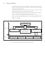
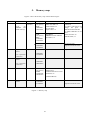
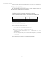
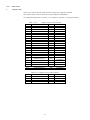
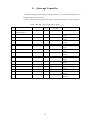
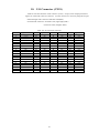
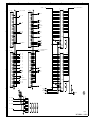
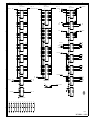
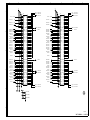
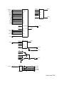
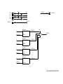
1
SH7751R Solution Engine TM (MS7751RSE01) User’s Manual 4th Edition Hitachi ULSI Systems Co., Ltd. MS7751RSE01-M Cautions 1. Products and product specifications are subject to change without notice. 2. Hitachi ULSI Systems Co., Ltd. makes every attempt to ensure that the information of this manual is correct and reliable; however, Hitachi ULSI Systems Co., Ltd. takes no responsibility for damages or infringement of patent rights or other rights derived from the use of the information, product or circuit. 3. This manual does not authorize the use of the patent rights or other rights of third parties or Hitachi ULSI Systems Co., Ltd. 4. No one is permitted to reproduce or duplicate, in any form, the whole or part of this document without written approval from Hitachi ULSI Systems Co., Ltd. 5. The product overview described in this manual may differ slightly from the actual product. Notes on Using the SH Solution Engine This section contains topics to be carefully read and considered when using the SH Solution Engine (referred to as Solution Engine) of the Hitachi ULSI systems. (Solution Engine Components) 1. After opening the package, check the following items to confirm that everything is in place. a. Solution Engine main unit b. CD-ROM (A set of software, User’s manual) c. Monitor EPROM for big endian d. Software license agreement (How to connect the Solution Engine) 2. Before connecting the power supply, cables, development equipment and a daughterboard, the power must be turned off. 3. Before turning on the power following the connection of cables and other equipment, check all connections again to be sure that the wiring and polarity are correct. (Installation) 4. Do NOT touch some parts on board during operating, because their temperature is high. Whenever you want to touch them, you must turn off the power and keep enough time to cool down. 5. The Solution Engine is developed for evaluation of products before they are put under the development phase. Do not incorporate the Solution Engine into any of the products. 6. Do not install the Solution Engine in an area subject to direct sunlight and other areas exposed to heaters or other source of high temperatures. 7. Do not choose area subject to extremely dusty condition. 8. Use care to keep the board free from contact with pieces of wire, soldering waste and other foreign matter. (Restriction) 9. OS of the host system connected and checked before shipping the Solution Engine is Windows 95. In using Solution Engine by OS other than Windows 95, please use after checking enough. 10. Please connect the included power supply adapter to the Solution Engine. Although the power supply terminal stand is mounted in Solution Engine, please do not use it as much as possible. 11. When using Ethernet, be sure to connect through a hub. It may be unable to communicate, if Solution Engine is connected directly to PC via a cross cable. 12. Ethernet may encounter an abrupt drop of signal level and the line cannot be connected depending on the number of hub line connections or cable length. So that if the Solution Engine is connected to a hub, reduce the number of lines connected to a hub to a minimum to ensure reliable operation. 13. The ROM emulator controls reset and NMI while the ROM emulator is used. Do not actuate reset switch (SW2) and abort switch (SW3) during the ROM emulator is used. (1) 14. The free warranty period of the system is one year from the delivered day. But it is limited to systems that are being used under normal condition such as environment condition, the way to operate the Solution Engine. 15. The warranty is void in the following cases. a. Any problems of system caused by natural disaster. b. Systems that are modified and repaired by user c. Any problems caused by improper handling 16. Do not reprovide the Solution Engine to the people who use the Solution Engine to hinder international peace and safety and do not use the Solution Engine for such aims personally and do not have third parties use the Solution Engine for such aims. For exporting the Solution Engine, follow Foreign Exchange and Foreign Trade Control Low and prescribed procedure. (2) Components of the Solution Engine Open the package and check the contents to match against the packing list. Table 0.1 lists the components of the Solution Engine. Figure 0.1 shows the contents of the Solution Engine. Table 0.1 Solution Engine components No Item Description 1 SH7751R Solution Engine SH7751R Solution Engine Hardware 2 CD-ROM (Software, User’s manual) C compiler (Trial Version), driver software source file, various header file, User’s manual 3 Monitor EPROM Monitor EPROM for big endian 4 Software License Agreement Condition to use software Vx.xB ×2(included) 2 CD-ROM 1 SH7751R Solution Engine main unit 3 Monitor EPROM for big endian 4 Software license agreement Figure0.1 Components of the Solution Engine (3) Table of Contents Notes on Using the SH Solution Engine ………… (1) Components of the Solution Engine …………(3) Table of Contents 1. Features of the Solution Engine 1.1 2. Features of the Solution Engine ………… 1 1.2 Debugging Function ………… 1 1.3 System Configuration ………… 2 1.4 Software Configuration ………… 4 1.5 Solution Engine Specifications ………… 5 Setting the Solution Engine ………… 6 2.1 Connecting the Host System ………… 9 2.2 Connecting the E10A Emulator 2.3 3. ………… 1 Connecting the Power ………… 11 ………… 12 Switch Functions ………… 13 3.1 Switch (SWn) Functions ………… 13 3.2 Jumper Pin Functions ………… 18 3.3 Test Pin Functions ………… 20 4. LED Functions ………… 21 5. Memory Map ………… 22 6. Hardware Configuration ………… 24 7. Function Blocks ………… 26 7.1 Ethernet Control 7.2 Serial Control ………… 36 7.3 Super I/O Control 7.4 Memory Block 7.5 General-purpose switches 7.6 8-bit LED 8. Interrupt Controller ………… 55 9. Expansion Slot (CN1) ………… 56 ………… 26 ………… 49 ………… 52 ………… 53 ………… 54 9.1 Expansion Slot Pin Assignments ………… 56 9.2 Expansion Slot Connector configuration………… 58 9.3 Daughter Board Dimensions ………… 58 (4) 10. I/O Connector (CN18) ………… 59 11. Bus Controller Setting ………… 60 12. SH7751R CPU Bus interface 13. Monitor program usage ………… 62 ………… 61 13.1 Monitor program usage ………… 62 13.2 Monitor program function ………… 71 14. Description of Command 15. Appendix ………… 72 ………… 80 15.1 Board Dimension ………… 81 15.2 Circuit Diagram ………… 83 15.3 FPGA Logic ………… 110 15.4 Parts List ………… 130 (5) 1. Features The Solution Engine is a system capable of efficiently developing software and hardware for systems that employ the Hitachi SH7751R (SH-4) 32-bit SuperH series microcomputer. 1.1. Features of the Solution Engine The Solution Engine has the following features. 1. All the information concerning this board including the circuit diagrams, various connector specifications, and the internal logic of the FPGA used with the board are contained in the manual. 2. The specification of this board is a summary of the proposals presented by Real Time OS manufacturers and many middleware development manufacturers. This is why hardware is configured so as to render OS and middleware easily portable. 3. Ethernet controller, PCMCIA controller, serial controller and other peripherals are off-theshelf purchases. 4. Because Ethernet, PCMCIA, serial controllers and similar hardware are loaded on the board, system development is easier with these pieces of hardware applied. 5. The Solution Engine has the expansion slot outputting address bus and control signals of the SH7751R so that a user’s hardware can be connected. 6. The Solution Engine has an I/O bus which carries an SH7751R port and the output of the timer output terminal. 7. 1.2. The Solution Engine has CPU bus interface connector so as to trace SH7751R bus signal. Debugging Function The Solution Engine has a monitor program on the board. The monitor program has the following debugging functions. 1. Execution and pause of user programs The program can be executed from an optional address. When the following condition arises, the user program halts. 2. a. When a break point is detected. b. When the Reset switch or Abort switch is pressed. Display and change of register contents The contents of the general-purpose register can be displayed and changed as required. 3. Display and change of memory contents Memory contents can be expressed in mnemonic or hexadecimal numbers and changed as required. 1 1.3. System Configuration Figure1.1 shows a system configuration of the Solution Engine. Figure1.2 shows an external overview of the Solution Engine. Connect a host system, a modem and an Ethernet Hub to the Solution Engine according to the debugging environment and peripherals such as a modem. User must prepare a host system, a modem and an Ethernet hub. The host system, the modem, the Ethernet hub and power supply used to check the operation before shipping are as follows. (Host system) Hitachi FLORA310 and 330 (Windows 95 machine with 9-pin serial connector) (Modem) Microcom V.34ES II (Ethernet Hub) 8-Port Ethernet Hub (Power supply) ATX power supply [Notes] Ethernet may encounter an abrupt drop of signal level and the line cannot be connected depending on the number of hub line connections or cable length. When connecting the Solution Engine to the hub, reduce the number of lines connected to the hub to a minimum to ensure reliable operation. * Windows is a trademark of U.S. Microsoft Corporation. ATX power supply 5V, 12V, 3.3V Solution Engine AC 110V power supply PC card Host system (FLORA310 or equivalent) 10BASE-T Cable Ethernet Hub Modem RS-232C cross cable Figure1.1 System configuration of the Solution Engine 2 Ethernet 100BASE-T RJ-45 connector PS2 connector (Top: Mouse, Bottom: Keyboard) IEEE1284 parallel port connector LED for LAN CN12 M9 NM93C46 SCIF CN2 USB LVC374A (M1543C SCI) ISA slot UART CN3 U1 U2 U3 SP211E U6 CN6 CN4 CN7 PS2x2 CN5 USB connector (Top: CN0, Bottom: CN1) U5 U4 H1081 SP211ECA 0018 SH7751R I/O connector CN19 CN20 SP211ECA 0018 AM79C973A MBM29LV160T C41 U9 CBTD3384 M2 U12 U10 MBM29LV160T U13 CBTD3384 M3 OSC3 uPD45128841 CN8 PCI Slot 1 SH7751R CPU bus Interface M1 SH7751R E10A connector U11 HD6417751R CBTD3384 3.6864 MHz (For EPM) CY2308SC-1 U14 EPM7128ATC 100-7 HAD279949 M5 CBTD3384 J4 uPD45128841 Expansion slot U16 U15 CBTD3384 CN18 Port I/F 5.0V PCI slot CN9 PCI Slot 2 J1 U19 (For FCT3805) 48MHz CN11 CN10 ISA Slot 2 ISA Slot 1 SW7 SW5 CN 17 OSC1 14.3181 MHz (For M1543C) U24 U27 LS245 U32 U34 LVC14 LSO7 SW8 16bit generalpurpose switch1 U21 U22 U23 CARD SLOT U28 U26 U25 U29 U30 U31 LVC245A LVC245A LVC245A LVC245A SW9 CN21 TPS2211 LVC08 CN32 (CR2032 holder) U20 LVC244A LVC244A LVC244A LVC244A FCT3805 SW4 (For M1543C/USB) M1543C B1 MR-SHPC-01 V2 U 18 33MHz OSC5 20MHz (For SH7751R) OSC2 SW6 CN1 ETX-BUS U17 OSC4 16bit general-purpose switch0 M8 27C160 27C800 U35 U36 CN22 M7 27C160 27C800 CN23 RTC6593 U33 LM1085 IT-3.3 CR2032 CN30 CN29 CN28 CN27 CN26 CN25 CN13 FDD connector IDE 1 CN15 EPF10K30ATC 144-2 DCA519931 CN16 40pin IDE connector (Primary) CN24 J2 FDD J3 CN14 IDE 2 SW1 POWER 40pin IDE connector (Secondary) Power supply switch M11 SW3 SW2 RESET NMI Reset switch Abort switch System LED (Reset etc.) Connector for ATX power 8 bit LED C113 LED for PC CARD Figure1.2 SH7751R Solution Engine External view EPC 1441PC8 1.4. Software Configuration The Solution Engine has a monitor program in EPROM. The monitor program displays memory data and executes programs transferred to user memory. The user program can be executed and evaluated by connecting the host system. For connection between host system and the Solution Engine, terminal software such as hyper terminal mounted as a standard accessory of Windows 95 can be used. The source programs input by using various editors can be converted into machine language by using the C compiler, the assembler, the linkage editor and the object converter. Figure1.3 shows software configuration when the Solution Engine is connected to the host system. For more details on the functions and the usage of the supplied software, refer to ReadMe.txt in the CD-ROM. Host system OS Host system Editor Interface software (Hyper terminal etc.) C compiler (SHC.EXE) Cross assembler (ASMSH.EXE) Linkage editor (LNK.EXE) Serial interface Monitor program Solution Engine User program execution control function Break function Reverse assembler function Figure 1.3 Software Configuration when connected to the Host System 4 Memory control function 1.5. Solution Engine Specifications Table1.1 lists the functional specifications of the Solution Engine. Table1.2 lists the specifications for the power supply, dimensions and environmental factors. Table 1.1 Functional Specifications of the Solution Engine Item Subject device System Clock User memory ROM Flash ROM EPROM Ethernet PCMCIA Serial Interface Super I/O (Expansion Board) Monitor Program Host System Host Interface Command Components Specifications SH7751R(SH-4 PCI) Operation frequency: Internal 240MHz, External: 60MHz(Maximum 81MHz*) (20MHz oscillation module is equipped) Oscillation module model name: SG-8002DC-20M-PTCB(SEIKO-EPSON) 64-MByte SDRAM(Cycle time: 10ns) SDRAM model name: uPD45128841G5-A75-9JF (ELPIDA) 4-Mbyte Flash ROM model name: MBM29LV160T-90PFTN (Fujitsu) 2-Mbyte(mounted) EPROM model name: MX27C8100PC-10 (MACRONIX) 10/100BASE-TX 1ch Controller model name: Am79C973AVC(AMD) 1 slot Controller model name: MR-SHPC-01 V2 (Marubun) 1ch Controller: SH7751R on-chip SCIF Serial 2ch, Parallel 1ch, IDE 2ch, FDC 1ch, USB 2ch, PS2(Keyboard/Mouse) 2ch mounted Controller model name: M1543C B1(ALi) FLORA310 or equivalent (Windows95 or Windows98 is equipped) RS-232C interface 9 pin connector used (Transfer speed: 9600, 19200, 38400, 115200bit/s) 17 commands ML(Memory Load), RR(Register Read), RW(Register Write), RC(Register Clear), ME(Memory Edit), G(Go), BS(Breakpoint Set) and etc. Solution Engine, CD-ROM (User’s manual) and etc. (Note)* MS7751RSE01 can be execute external 81MHz except for PCMCIA as maximum. 66MHz specification. Table 1.2 Power Supply, Dimensions and Environmental Factors of the Solution Engine Item Environment Operating voltage Current consumption External dimension Specifications Operating conditions - Temperature: 10-35 degree C - Humidity: 30-85%RH (no condensation) - Ambient gas: Should not have corrosive gas DC3.3V, 5.0V, 12V (Off-the-shelf power supply for ATX should be used) 1A (temporary value) ATX size 304.8mm× 243.84mm 5 2. Setting the Solution Engine After opening the package, set the Solution Engine as follows. 1. Choosing the debugging environment The Solution Engine has a monitor program stored in EPROM. Connect the host system equivalent of FLORA310 to use the monitor program. The monitor program is an implementation of the basic functions including reference and change of memory data and execution of programs. Use E10A emulator for trace of user programs and other debugging. 2. Connecting a daughterboard When using a daughterboard, connect the cable to the expansion slot (CN1) on the Solution Engine. 3. Connecting the modem Connect the modem to M1543C B1 COM1 connector (CN3). M1543C B1 COM1 connector outputs all signals necessary for connection of the modem. 4. Connecting the LAN Connect the LAN to the RJ-45 connector (CN7) via the Ethernet hub. 5. Connecting the I/O board Use the I/O connector (CN18) to use SH's general-purpose I/O port. The I/O connector outputs all general-purpose ports of the microcomputer. 6. Setting Jumper Pins and DIP SW Set jumper pins and the DIP SW according to the operating condition. 7. Connecting the power supply Connect power supply cable of ATX power to CN16. Do not connect to CN16 while ATX power supply remains connected to AC110V. [Notes] (1) Before connecting ATX power supply to the 110V AC power following upon completion of Steps 1 through 7 above, recheck that connection of the board and a cable, and setting of jumper pins and DIP switches are correct. (2) When using Ethernet, be sure to connect through HUB. It may be unable to communicate, if the Solution Engine is connected directly to PC via a cross cable. 6 Figure 2.1 shows the procedure to install the Solution Engine. Start Installation Open the package and check the contents to match against the packing list. Use the limited monitor program Use development device? N (Little endian) Use big endian? Y (Big endian) Remove EPROM(MX27C8100) on 42-pin IC socket M7 and M8 from the IC socket. Mount monitor EPROM (Vx.xB) for big endian on a 42-pin IC socket M7 and M8. Turn SW4-6 ON Use ROM emulator Connect ROM emulator to 42-pin IC socket M7 and M8. Connect the daughterboard? Connect CN2 to host system via RS232C cable (9pin cross cable) N Y Connect the daughterboard to expansion slot (CN1) Use RS-232C connector CN3? N Y Connect a cable to RS-232C connector CN3 N Use LAN(10BASE-T)? Y Connect 10BASE-T cable to CN7 Connect I/O board using SH7751 port and private pin? N Y Connect I/O board to CN18. N Use keyboard and mouse? Y Connect keyboard and mouse to CN5. Connect USB function device? N Y Connect USB function device to CN6. Figure 2.1 Installing the Solution Engine 7 Mount monitor EPROM (Vx.xA) for big endian on a 42-pin IC socket M7 and M8. Turn SW4-6 OFF N Use IEEE1284 board? Y Connect IEEE1284 cable to CN4 N Mount PCI board? Y Mount PCI board to CN8 and CN9. N Mount ISA board? Y Mount ISA board to CN10 and CN11. N Use IDE? Y Connect IDE cable to CN13(primary) and CN14(secondary) N Connect FDD? Y Connect FDD to CN15 Set jumper pin Connect ATX power supply to the Solution Engine Installation is completed Figure2.1 Installing the Solution Engine 8 2.1. Connecting the host system To use the monitor program, connect the host interface connector (CN2) to the host system via an interface cable. Figure2.2 shows how to connect the host system. Host Interface Cable (9 pin cross cable) Host System (FLORA310 or equivalent) CN2 Figure 2.2 Connecting the host system 9 1. Host Interface Cable For example, Figure 2.3 shows the wire connection when FLORA310 is connected to the Solution Engine. The Solution Engine can be connected to the host system via an off-the-shelf 9pin cross cable. FRORA310 (9pin connector) 2Pin 3Pin 5Pin 7Pin 8Pin Solution Engine CN2 RxD TxD GND RTS CTS RxD TxD GND RTS CTS DTR DSR 2Pin 3Pin 5Pin 7Pin 8Pin 4Pin 6Pin Figure 2.3 Wire connection between FLORA310 and the Solution Engine 2. Transfer Speed Setting 9600, 19200, 38400 and 115200 bit/s can be selected as a transfer speed with DIP switches (SW5-1, SW5-2) on the Solution Engine. Set the DIP switch according to the transfer rate. For specifications of the DIP switch, refer to Section 3.1 (4), “ DIP switch(SW5) for setting baud rate”. 3. Host Interface Connector (CN2) Figure 2.4 shows the pin assignments of the host interface connector (CN2) and the list of signals. 1 2 3 4 5 6 7 8 9 Pin code I/O Name 1 (NC) 2 RxD Input Receive data 3 TxD Output Send data 4 DTR Output data terminal ready 5 GND 6 DSR Input data set ready 7 RTS Output Request to send 8 CTS Input Clear to send 9 (NC) ground Figure 2.4 Pin Assignments (CN2) 10 2.2. Connecting the E10A emulator This Solution Engine has a debugging chip(*Note) on the SH7751R, and SH7751R E10A emulator can be used. Figure2.5 shows how to connect the E10A emulator. The PCMCIA card emulator that is main unit of SH7751R E10A emulator can be connected to the connector (CN19) via H-UDI port (Hitachi-User Debug Interface). The E10A emulator connectable to the Solution Engine is as follows. For more details on the connecting method and the E10A emulator setup, refer to the following manual. Hitachi Co., Ltd. E10A emulator HS7751RKCM02H(PCMCIA) *Note: Debugging chip is same as actual chip. E10A HITACHI E10A main unit (PCMCIA card) HS7751RKCM02H User Interface Cable CN19 AUD connector Figure 2.5 Connecting the E10A emulator 11 2.3. Connecting the power supply 1. Connecting ATX power supply SH7751R Solution Engine uses ATX power supply (option product) as a power supply. Connect the power supply to AC110V as shown in figure2.6. [Notes] Before connecting the power adapter, recheck the board and cable are correctly connected, and check the jumper pins and DIP switch are correctly set. ATX power supply 5V,12V,3.3V Solution Engine AC 110V power supply PC card CN16 Figure 2.6 Connecting the power source 12 3. 3.1. Switch (SWn) functions 1. Power supply switch (SW1) Switch Functions This switch is to turn ON and OFF power supply of SH7751R Solution Engine. This switch is a push button switch. Power supply is turned to ON or OFF by pushing this switch. Figure 3.1 Power supply switch 2. Reset Switch (SW2) This switch is to reset microcomputer. This switch is a push button switch. The microcomputer is reset by pushing this switch. Reset is cleared by releasing this switch [Notes] While ROM emulator is used, ROM emulator controls reset of the microcomputer. Do not operate the reset switch when connecting the ROM emulator. Figure 3.2 Reset switch 13 3. Abort switch(SW3) This switch controls NMI pin of the microcomputer. This switch is a push button switch. NMI pin is turned to Low by pushing this switch. NMI pin is turned to High by releasing this switch. [Notes] ROM emulator controls NMI pin while ROM emulator is used. Do not operate the abort switch when connecting ROM emulator. Figure 3.3 Abort switch (SW3) 14 DIP switch for setting microcomputer operating mode(SW4) Figure3.4 shows the DIP switch for setting microcomputer operating mode (SW4). Table3.1 shows switch functions. This switch is connected to mode pins (MD0-MD5) of the SH7751R. This switch can select the operating mode and endian as shown in table3.1. This switch must be switched while the power supply is in OFF state. 6 5 4 3 2 O N SW4 1 4. SW4-6 SW4-5 SW4-4 SW4-3 SW4-2 SW4-1 Figure3.4 DIP switch for setting microcomputer operating mode(SW4) Table3.1 Functions of SW4 SW SW4-1 SW4-2 SW4-3 Name Microcomputer operating mode setting switch SW4-4 SW4-5 Area0 bus select switch width SW4-6 Endian select switch Function SW4-1 to SW4-3 is connected to mode pins MD0 to MD2, and this switch selects clock operating mode of the SH7751R. SW4-1 SW4-2 SW4-3 MD[0:2] ON ON ON 000 Clock operating mode Mode0 OFF ON ON 100 Mode1 ON OFF OFF OFF ON ON 010 110 Mode2 Mode3 ON ON OFF 001 Mode4 OFF ON OFF 101 Mode5 remarks At shipment SW4-4 and SW4-5 are connected to mode pins MD3 and MD4, and select bus width of Area0 (CS0). Bus width is fixed to 32-bit. SW4-4 and SW4-5 must be used in OFF state. SW4-6 is connected to mode pin MD5 of the SH7751R, and select big endian or little endian. [ON] Big endian [OFF] (At shipment) Little endian 15 DIP Switch for setting baud rate(SW5) Figure3.5 shows DIP switch for setting the baud rate (SW5). Table3.2 lists the functions of the switch. As listed in Table3.2, this switch can select the baud rate of the SH7751R on-chip SCIF and ROM placed at area0. 8 7 6 5 4 3 N 2 O SW5 1 5. SW5-5, SW5-7, SW5-8 are not used SW5-6 SW5-4 SW5-3 SW5-2 SW5-1 Figure 3.5 DIP Switch for setting the baud rate(SW5) 16 Table3.2 SW5 Functions SW SW5-1 SW5-2 Name SH7751R SCIF baud rate select switch Function Select the baud rate of SH7751R on-chip SCIF2 (SCI with FIFO). [SW5-1: OFF, SW5-2: OFF] (At shipment) 9600bit/s [SW5-1: ON, SW5-2: OFF] 119200bit/s [SW5-1: OFF, SW5-2: ON] 38400bit/s [SW5-1: ON, SW5-2: ON] 115200bit/s SW5-3 SW5-4 ROM select switch Select ROM placed at h’0000000-h’00FFFFFF and h’01000000-h’01FFFFFF. [SW5-3: ON, SW5-4: ON](At shipment) h’00000000-h’003FFFFF: EPROM h’01000000-h’013FFFFF: Flash ROM [SW5-3: OFF, SW5-4: ON] h’00000000-h’003FFFFF: Flash ROM h’01000000-h’013FFFFF: EPROM [SW5-3: ON, SW5-4: OFF] h’00000000-h’003FFFFF: CPU bus I/F connector(CN20) h’01000000-h’013FFFFF: Flash ROM [SW5-3: ON, SW5-4: OFF] h’00000000-h’003FFFFF: CPU bus I/F connector(CN20) h’01000000-h’013FFFFF: EPROM SW5-6 CS6 on-board resource select switch Select whether to use peripheral LSI of CS6 area on the Solution Engine. [SW5-6: ON] (At shipment) Use peripheral LSI of CS6 area. [SW5-6: OFF] Peripheral LSI (MR-SHPC-01) placed at CS6 area is allocated at CS1. All space of CS6 is allocated to expansion slot. This switch can be used for evaluating a daughterboard using CS6. SW5-5 SW5-7 SW5-8 For test(Not used) This switch is for testing. [SW5-5: ON, SW5-7: ON, SW5-8: ON] (At shipment) Do not change the factory-shipped setting. 17 3.2. Jumper Pin (Jn) Functions 1. Test Jumper1 (J1) This jumper is the jumper for testing SH7751R PCIC. Table 3.3 shows the function of the jumper for testing SH7751R PCIC. This jumper must be used while pins 1-2 are closed. When pins 2-3 are closed, microcomputer does not work. Table3.3 Functions of the jumper for testing SH7751R PCIC (J1) Jumper Pin name Jumper Pin Connected State J1 J1 1 Function Input 33MHz to SH7751 PCICLK.(at shipment) 3 (1-2pin closed) Power supply is not provided to SH7751 PCICLK. J1 1 3 (2-3pin closed) 2. Test jumper2 (J2) This jumper is the jumper for testing NMI pin. Table3.4 shows the function of the jumper for testing NMI pin. Use this jumper while pins 1-2 are closed. When pins 2-3 are closed, the microcomputer does not work. Close pins1-2 and connect NMI clip to TP3 while ROM emulator is used. Table3.4 Function of the jumper for testing NMI pin (J2) Jumper Pin name Jumper Pin Connected State J2 J2 1 3 (1-2pin closed) J2 1 3 (2-3pin closed) Function Abort switch can control NMI pin of the SH7751.(at shipment) Close 1-2pin and connect NMI clip to TP3 when connecting ROM emulator by using ROM socket Abort switch makes NMI pin of the SH7751 unconnected, NMI pin is connected to CPU bus interface. Close 2-3pin when connecting ROM emulator by using CPU bus interface connector. 18 3. Test Jumper3 (J3) This jumper is the jumper for testing ATX power supply control. Table3.5 shows the function of the jumper for testing ATX power supply control. Use this jumper with 2-3pin closed. When 1-2pin is closed, ATX power is in ON state at all times, and the power supply switch on the Solution Engine become invalid. Table3.5 Function of the jumper for testing ATX power supply control Jumper Pin name Jumper Pin Connected State J3 J3 1 3 Function ATX power supply is in ON state, and power supply is provided to the Solution Engine all the time. (1-2pin closed) J3 1 3 Power supply switch(SW1) on the Solution Engine controls ON/OFF of ATX power supply.(at shipment) (2-3pin closed) 4. Expansion slot 5V power supply(J4) Table3.6 shows the function of the expansion slot 5V power supply jumper (J4). As shown table3.6, this jumper connects pins A66 and A67 of the expansion slot to 5V power supply on the Solution Engine. When mounting LSI or IC that need analog 5V power supply, analog 5V power can be provided from pins A66 and A67 of the expansion slot by closing J1. Signals of address bus and data bus output to the expansion slot are 3.3V. Mount 3.3V→5V interface IC on a daughterboard if 5V interface is necessary. Table 3.6 Function of the expansion slot 5V power supply jumper (J4) Jumper Pin name Jumper Pin Connected State J4 J4 1 2 (Closed) J4 1 2 Function Pins A 66 and A67 of the expansion slot are connected to A+5V of the Solution Engine. In this state, A+5V power is provided to the daughterboard. Power supply switch on the Solution Engine controls ON/OFF of ATX power. (Open) 19 3.3. Description of test pin (TPn) Table 3.7 lists the function of test pins. Table 3.7 Test Pin Functions Test Pin Function TP1 For test (Flash Ready/Busy) TP2 RESET-IN (Connect RESET probe when using IC socket-equipped ROM emulation ) TP3 NMI-IN (Connect NMI probe when using IC socket-equipped ROM emulator) TP4 For test (Super I/O) TP5 For test (Super I/O) TP6 For test (Super I/O) TP7 For test (Super I/O) TP8 For test (Super I/O) TP9 For test (Super I/O) TP10 For test (Super I/O) TP11 For test (Super I/O) TP12 For test (Super I/O) TP13 For test (Super I/O) TP14 For test (Super I/O) TP15 For test (Super I/O) 20 4. LED Functions 1. Power LED (LED17) This LED indicates that the power is supplied correctly. Function is as follows. LED ON: Power is supplied to the Solution Engine. LED OFF: Power is not supplied to the Solution Engine. 2. CPU Status LED (LED9-LED12) This LED indicates CPU operation. Function is as follows. LED9 ON: CPU is in RESET mode. LED10 ON: CPU is in SLEEP mode. LED11 ON: CPU is in STANBY mode. LED12 ON: CPU is under operating condition 3. PC card detection LED (LED13) This LED indicates that the PCMCIA controller detects the PC card normally. LED ON: PC card is detected. LED OFF: PC card is not detected. 4. Ethernet line monitor LED (CN7-LED1 CN7-LED2, LED14-LED15) This LED indicates presence or absence of transmit signal and receive signal and connected condition of Ethernet line. For mode details on LED, refer to Section7, “Function block”. 5. HDD access LED (LED16) This LED indicates access condition to HDD. Function is as follows. LED ON: Accessing to HDD LED OFF: Not accessing to HDD. 6. 8-bit LED (LED1-LED8) This LED is 8-bit LED that can turn ON and OFF LED via register allocated to memory map of the Solution Engine. For mode details on usage, refer to Section7, “Function block”. 21 5. Memory map Figure5.1 shows the memory map of the Solution Engine. Area No. Area 0 Space name ROM Area Bus width 32Bit (5WAIT) (Area for EPROM and Flash memory) Space 16MB Real capacity (4MB) h’00000000h’003FFFFF Device EPROM MX27C8100PC-10 (MACRONIX)×2 or equivalent 42pin socket ×2 16MB Real capacity (4MB) h’01000000h’013FFFFF FlashROM MBM29LV160T-90PFTN (FUJITSU) ×2 32MB h’02000000h’03FFFFFF Area1 Area2 Expansion Area1 (On expansion connector) Expansion Area2 Option SDRAM Area Expansion area0 Expansion slot/CS0 assert 64MB Expansion area1 Expansion slot/CS1 assert Expansion area2 Expansion slot/CS2 assert h’04000000h’07FFFFFF Option 64MB h’08000000h’0BFFFFFF (On expansion connector) Area3 Remarks (1) ROM emulator can be connected. (2) SW5-3 and SW5-4 can change the place of EPROM and Flash ROM. (3) 8Mbit EPROM can be used. MX27C8100PC-10 (MACRONIX) ×2 32Bit 64MB Real capacity (64MB) h’0C000000h’0FFFFFFF Device Model name: UPD45128841G5-A75-9JF (ELPIDA) ×4 (128M SDRAM) Area4 Expansion Area4 Option 64MB h’10000000h’13FFFFFF Expansion Area4 Expansion Area4 Expansion slot/CS4 assert Figure5.1 Memory map 22 Area No. Area5 Area6 Space name Expansion Area5 (on expansion connector) Bus width Option 16Bit Peripheral device control register 16Bit (3WAIT) Space 64MB h’14000000h’17FFFFFF Device Expansion Area5 16MB h’18000000 -h’18FFFFFF Card controller LSI area manufactured by MARUBUN Model name: MR-SHPC-01 V2 General-purpose switch area Memory and register must access to this area. 16MB h’1A000000 -h’1AFFFFFF Area for debug LED Area for debug LED Single LED ×8 16MB h’1B000000 -h’1BFFFFFF Test mode area Area for testing the Solution Engine. This address is not open to users. Do not access to this area. Expansion slot/CS5 assert 16MB h’19000000 -h’19FFFFFF Area7 SH7751R incorporated - Remarks Expansion Area5 h’1C000000 -h’1CFFFFFF H’1D000000 -h’1DFFFFFF PCI memory space Access area H’1E000000 -h’1E1F0000 h’1E200000 -h’1E2000FF PCIC register PCI configuration register area h’1E20010 -h’1E200227 PCIC register PCIC local register area H’1E200228 -h’1E23FFFF h’1E240000 -h’1E27FFFF PCI I/O space Access area H’E280000 -h’1FFFFFFF Figure5.1 Memory map 23 This area reads generalpurpose register ×2 6. Hardware Configuration Figure6.1 shows the block diagram of Solution Engine. As figure6.1 shows, there are 3.3V bus, 5V bus and PCI bus. 1. 3.3V Bus Memory including SDRAM and Flash ROM are connected to 3.3V Bus to execute user program at high-speed. 2. 5V Bus EPROM is 5V bus interface. EPROM is connected to SH via 3V→5V conversion buffer. 3. PCI Bus This PCI Bus used SH7751R PCIC. M1543C B1, Am79C973AVC and 2slot of PCI bus slot are connected to PCI bus. 24 5V Interface 3.3V Interface PCMCIA card slot (CN17) Expansion slot (CN1) MRSHPC -01 V2 16bit DIP switch 8bitLED 64MB SDRAM (UPD45128841 G5-A75-9JF) x4 4MB FlashROM FPGA (MBM29LV16 0T) x2 (EPF10K 30TC144) SH BUS 4MB EPROM (MX27C 8100PC-10) HD74LVC244AT SH BUS 3.3-5V Conversion SH bus I/F Connector(CN20) AUD connector(CN19) SH7751R RJ-45(CN7) FPGA (EPM7128 ATC100) PortI/O connector(CN18) SCIF connector(CN2) PCI BUS Pulse Transformer (H1081) RS232C Driver Ethernet Controller (AM79C973AVC) PCI Bus slot (CN9) PCI Bus slot (CN8) PCI BUS 3.3-5V Conversion FDD connector(CN15) IDE connector(CN13) SuperI/O (M1543C B1) IDE connector(CN14) PS2 connector(CN5) PRN connector(CN4) USB connector(CN6) SCI connector(CN3) SCI connector(CN12) ISA BUS RS232C Driver ISA Bus slot (CN10) Figure6.1 Block diagramof the Solution Engine ISA bus slot (CN11) 7. 7.1. Ethernet Control 1. Block description Function Block Figure7.1 shows a block diagram of the Ethernet control block. The Ethernet control block has a controller (Am79C973A manufactured by AMD), serial EPROM (NM93C46) and a pulse transformer (H1081 manufactured by Pulse Engineering), and provides Ethernet-interface at 10BASE-T/100BASE-TX via RJ-45 connector CN7. Other features include LEDs (CN7-LED1, CN7-LED2, LED14-LED15) used to indicate the presence of reception signals. In addition, a 25MHz crystal oscillator (× 3) is mounted as the operation clock of Am70C973A. Am79C973A Main memory SH7751R PCI bus System bus Figure 7.1 Ethernet Control Block Diagram 26 2. Memory Map Figure 7.2 shows a memory map of the Ethernet controller. Am79C973AVC uses 32byte(h’00-h’1F) on PCI bus. Address of the memory map is offset address. Address on the PCI bus is decided by adding the set PCI base address. Am79C973AVC can be assigned to both memory and I/O, because Am79C973AVC is connected to device number0 (IDSEL=AD16). DWIO=0 h’00 h’0F h’10 h’12 h’14 h’16 h’18 h’1F DWIO=1 h’00 h’0F h’10 APROM RDP APROM RDP RAP h’14 RAP Reset Register h’18 Reset Register h’1C BDP Reserved Figure 7.2. Ethernet memory map 27 BDP a. Am79C973AVC PCI Configuration register Table 7.1 shows a configuration of the PCI configuration register. The PCI configuration register is assigned to allocate Am79C973AVC on the PCI bus. Table 7.1. Configuration of DP83902A Register 31 24 23 Device ID Status 16 15 8 7 0 Vendor ID Command Base-Class Sub-Class Programming IF Revision ID Reserved Header Type Latency Timer Reserved I/O Base Address Memory Mapped I/O Base Address Reserved Reserved Reserved Reserved Reserved Subsystem ID Subsystem Vendor ID Expansion ROM Base Address Reserved CAP-PTR Reserved MAX_LAT MIN_GNT Interrupt Pin Interrupt Line PMC NXT_ITM_PTR CAP_ID DATA_REG PMCSR_BSE PMCSR Offset h’00 h’04 h’08 h’0C h’10 h’14 h’18 h’1C h’20 h’24 h’28 h’2C h’30 h’34 h’38 h’3C h’40 h’44 Reserved - Reserved h’FC 28 b. Control and Status register Table7.2 shows a configuration of Control and Status register. CSR sets address of CSR to RAP and accesses from RDP. Table7.2 Configuration of Control and Status register RAP Addr 00 Symbol Default Value Comments CSR0 uuuu 0004 Am79C973/Am79C975 Controller Status Register R 01 CSR1 uuuu uuuu Lower IADR: maps to location 16 S 02 03 CSR2 CSR3 uuuu uuuu uuuu 0000 Upper IADR: maps to location 17 Interrupt Masks and Deferral Control S S 04 05 CSR4 CSR5 uuuu 0115 uuuu 0000 Test and Features Control Extended Control and Interrupt 1 R R 06 CSR6 uuuu uuuu RXTX: RX/TX Encoded Ring Lengths S 07 08 CSR7 CSR8 0uuu 0000 uuuu uuuu Extended Control and Interrupt 1 LADRF0: Logical Address Filter — LADRF[15:0] R S 09 10 CSR9 CSR10 uuuu uuuu uuuu uuuu LADRF1: Logical Address Filter — LADRF[31:16] LADRF2: Logical Address Filter — LADRF[47:32] S S 11 CSR11 uuuu uuuu LADRF3: Logical Address Filter — LADRF[63:48] S 12 13 CSR12 CSR13 uuuu uuuu uuuu uuuu PADR0: Physical Address Register — PADR[15:0] PADR1: Physical Address Register — PADR[31:16] S S 14 CSR14 PADR2: Physical Address Register — PADR[47:32] S 15 CSR15 MODE: Mode Register S 16 17 CSR16 CSR17 uuuu uuuu see register description uuuu uuuu uuuu uuuu IADRL: Base Address of INIT Block Lower (Copy) IADRH: Base Address of INIT Block Upper (Copy) T T 18 19 CSR18 CSR19 uuuu uuuu uuuu uuuu CRBAL: Current RCV Buffer Address Lower CRBAU: Current RCV Buffer Address Upper T T 20 CSR20 uuuu uuuu CXBAL: Current XMT Buffer Address Lower T 21 22 CSR21 CSR22 uuuu uuuu uuuu uuuu CXBAU: Current XMT Buffer Address Upper NRBAL: Next RCV Buffer Address Lower T T 23 24 CSR23 CSR24 uuuu uuuu uuuu uuuu NRBAU: Next RCV Buffer Address Upper BADRL: Base Address of RCV Ring Lower T S 25 CSR25 uuuu uuuu BADRU: Base Address of RCV Ring Upper S 26 27 CSR26 CSR27 uuuu uuuu uuuu uuuu NRDAL: Next RCV Descriptor Address Lower NRDAU: Next RCV Descriptor Address Upper T T 28 29 CSR28 CSR29 uuuu uuuu uuuu uuuu CRDAL: Current RCV Descriptor Address Lower CRDAU: Current RCV Descriptor Address Upper T T 30 CSR30 uuuu uuuu BADXL: Base Address of XMT Ring Lower S 31 32 CSR31 CSR32 uuuu uuuu uuuu uuuu BADXU: Base Address of XMT Ring Upper NXDAL: Next XMT Descriptor Address Lower S T 33 CSR33 uuuu uuuu NXDAU: Next XMT Descriptor Address Upper T Note: u = undefined value, R = Running register, S = Setup register, T = Test register; all default values are in hexadecimal format. 29 Use Table7.2 Configuration of Control and Status register RAP Addr 34 Symbol Default Value Comments Use CSR34 uuuu uuuu CXDAL: Current XMT Descriptor Address Lower T 35 CSR35 uuuu uuuu CXDAU: Current XMT Descriptor Address Upper T 36 37 CSR36 CSR37 uuuu uuuu uuuu uuuu NNRDAL: Next Next Receive Descriptor Address Lower NNRDAU: Next Next Receive Descriptor Address Upper T T 38 39 CSR38 CSR39 uuuu uuuu uuuu uuuu NNXDAL: Next Next Transmit Descriptor Address Lower NNXDAU: Next Next Transmit Descriptor Address Upper T T 40 CSR40 uuuu uuuu CRBC: Current Receive Byte Count T 41 42 CSR41 CSR42 uuuu uuuu uuuu uuuu CRST: Current Receive Status CXBC: Current Transmit Byte T T 43 44 CSR43 CSR44 uuuu uuuu uuuu uuuu CXST: Current Transmit Status NRBC: Next RCV Byte Count T T 45 CSR45 uuuu uuuu NRST: Next RCV Status T 46 47 CSR46 CSR47 uuuu uuuu uuuu uuuu POLL: Poll Time Counter PI: Polling Interval T S 48 49 CSR48 CSR49 uuuu uuuu uuuu uuuu Reserved Reserved 50 CSR50 uuuu uuuu Reserved 51 52 CSR51 CSR52 uuuu uuuu uuuu uuuu Reserved Reserved 53 54 CSR53 CSR54 uuuu uuuu uuuu uuuu Reserved Reserved 55 CSR55 uuuu uuuu Reserved 56 57 CSR56 CSR57 Reserved Reserved 58 CSR58 59 CSR59 uuuu uuuu uuuu uuuu see register description uuuu uuuu 60 61 CSR60 CSR61 62 63 SWS: Software Style S Reserved T uuuu uuuu uuuu uuuu PXDAL: Previous XMT Descriptor Address Lower PXDAU: Previous XMT Descriptor Address Upper T T CSR62 CSR63 uuuu uuuu uuuu uuuu PXBC: Previous Transmit Byte Count PXST: Previous Transmit Status T T 64 CSR64 uuuu uuuu NXBAL: Next XMT Buffer Address Lower T 65 66 CSR65 CSR66 uuuu uuuu uuuu uuuu NXBAU: Next XMT Buffer Address Upper NXBC: Next Transmit Byte Count T T 67 68 CSR67 CSR68 uuuu uuuu uuuu uuuu NXST: Next Transmit Status Reserved T 69 CSR69 uuuu uuuu Reserved 70 CSR70 uuuu uuuu Reserved 30 Table7.2 Configuration of Control and Status register RAP Addr 71 Symbol Default Value Comments Use CSR71 uuuu uuuu Reserved 72 CSR72 uuuu uuuu RCVRC: RCV Ring Counter T 73 74 CSR73 CSR74 uuuu uuuu uuuu uuuu Reserved XMTRC: XMT Ring Counter T 75 76 CSR75 CSR76 uuuu uuuu uuuu uuuu Reserved RCVRL: RCV Ring Length S 77 CSR77 uuuu uuuu Reserved 78 79 CSR78 CSR79 uuuu uuuu uuuu uuuu XMTRL: XMT Ring Length Reserved S 80 81 CSR80 CSR81 uuuu 1410 uuuu uuuu DMATCFW: DMA Transfer Counter and FIFO Threshold Reserved S 82 CSR82 uuuu uuuu Transmit Descriptor Pointer Address Lower S 83 84 CSR83 CSR84 uuuu uuuu uuuu uuuu Reserved DMABA: Address Register Lower T 85 86 CSR85 CSR86 uuuu uuuu uuuu uuuu DMABA: Address Register Upper DMABC: Buffer Byte Counter T T 87 CSR87 88 CSR88 89 90 CSR89 CSR90 uuuu uuuu 262 5003 (Am79C973) 262 7003 (Am79C975) uuuu 262 uuuu uuuu 91 92 CSR91 CSR92 uuuu uuuu uuuu uuuu Reserved RCON: Ring Length Conversion 93 CSR93 uuuu uuuu Reserved 94 95 CSR94 CSR95 uuuu uuuu uuuu uuuu Reserved Reserved 96 97 CSR96 CSR97 uuuu uuuu uuuu uuuu Reserved Reserved 98 CSR98 uuuu uuuu Reserved 99 100 CSR99 CSR100 uuuu uuuu uuuu 0200 Reserved Bus Timeout 101 102 CSR101 CSR102 uuuu uuuu uuuu uuuu Reserved Reserved 103 CSR103 uuuu 0105 Reserved 104 105 CSR104 CSR105 uuuu uuuu uuuu uuuu Reserved Reserved 106 107 CSR106 CSR107 uuuu uuuu uuuu uuuu Reserved Reserved Reserved Chip ID Register Lower T Chip ID Register Upper T Reserved T S 31 Table7.2 Configuration of Control and Status register RAP Addr 108 Symbol Default Value CSR108 uuuu uuuu Reserved 109 CSR109 uuuu uuuu Reserved 110 111 CSR110 CSR111 uuuu uuuu uuuu uuuu Reserved Reserved 112 113 CSR112 CSR113 uuuu uuuu uuuu uuuu Missed Frame Count Reserved R 114 CSR114 uuuu uuuu Received Collision Count R 115 116 CSR115 CSR116 uuuu uuuu 0000 0000 Reserved On Now Miscellaneous S 117 118 CSR117 CSR118 uuuu uuuu uuuu uuuu Reserved Reserved 119 CSR119 uuuu 0105 Reserved 120 121 CSR120 CSR121 uuuu uuuu uuuu uuuu Reserved Reserved 122 123 CSR122 CSR123 uuuu 0000 uuuu uuuu Receive Frame Alignment Control Reserved S 124 CSR124 uuuu 0000 Test Register 1 T 125 126 CSR125 CSR126 003c 0060 uuuu uuuu MAC Enhanced Configuration Control Reserved T 127 CSR127 uuuu uuuu Reserved Comments 32 Use c. Bus Configuration register Table7.3 shows a configuration of the bus configuration register. BCR sets address of BCR to RAP and accesses from BDP. Table7.3 Configuration of the bus configuration register Name Programmability EEPRO User M No No RAP Mnemonic Default 0 MSRDA 0005h Reserved 1 2 MSWRA MC 0005h 0002h Reserved Miscellaneous Configuration No Yes No Yes 3 4 Reserved LED0 N/A 00C0h Reserved LED0 Status No Yes No Yes 5 LED1 0084h LED1 Status Yes Yes 6 7 LED2 LED3 0088h 0090h LED2 Status LED3 Status Yes Yes Yes Yes 8 9 Reserved FDC N/A 0000h Reserved Full-Duplex Control No Yes No Yes 10-15 Reserved N/A Reserved No No 16 17 IOBASEL IOBASEU N/A N/A Reserved Reserved No No No No 18 19 BSBC EECAS 9001h 0002h Burst and Bus Control EEPROM Control and Status Yes Yes Yes No 20 SWS 0000h Software Style Yes No 21 22 INTCON PCILAT N/A FF06h Reserved PCI Latency No Yes No Yes 23 24 PCISID PCISVID 0000h 0000h PCI Subsystem ID PCI Subsystem Vendor ID No No Yes Yes 25 SRAMSIZ 0000h SRAM Size Yes Yes 26 27 SRAMB SRAMIC 0000h 0000h SRAM Boundary SRAM Interface Control Yes Yes Yes Yes 28 29 EBADDRL EBADDRU N/A N/A Expansion Bus Address Lower Expansion Bus Address Upper Yes Yes No No 30 EBD N/A Expansion Bus Data Port Yes No 31 32 STVAL MIICAS FFFFh 0000h Software Timer Value PHY Control and Status Yes Yes No Yes 33 34 MIIADDR MIIMDR 0000h N/A PHY Address PHY Management Data Yes Yes Yes No 35 PCIVID 1022h PCI Vendor ID No Yes 36 37 PMC_A DATA0 C811h 0000h PCI Power Management Capabilities (PMC) Alias Register PCI DATA Register Zero Alias Register No No Yes Yes 38 39 DATA1 DATA2 0000h 0000h PCI DATA Register One Alias Register PCI DATA Register Two Alias Register No No Yes Yes 40 DATA3 0000h PCI DATA Register Three Alias Register No Yes 33 Table7.3 Configuration of the bus configuration register 4. Name Programmability EEPRO User M No Yes RAP Mnemonic Default 41 DATA4 0000h PCI DATA Register Four Alias Register 42 43 DATA5 DATA6 0000h 0000h PCI DATA Register Five Alias Register PCI DATA Register Six Alias Register No No Yes Yes 44 45 DATA7 PMR1 0000h N/A PCI DATA Register Seven Alias Register Pattern Matching Register 1 No Yes Yes No 46 PMR2 N/A Pattern Matching Register 2 Yes No 47 48 PMR3 Reserved N/A 0000h Pattern Matching Register 3 Reserved (for Am79C975) Yes Yes* No Yes* 49 Reserved 0000h Reserved (for Am79C975) Yes* Yes* 50 Reserved 0000h Reserved (for Am79C975) Yes* Yes* 51 52 Reserved Reserved 0000h 0000h Reserved (for Am79C975) Reserved (for Am79C975) Yes* Yes* Yes* Yes* 53 Reserved 0000h Reserved (for Am79C975) Yes* Yes* 54 Reserved 0000h Reserved (for Am79C975) Yes* Yes* Ethernet Line Monitor LED(CN7-LED1, CN7-LED2, LED14 to LED15) LEDs (CN7-LED1, CN7-LED2, LED14 to LED15) indicate the line condition of Ethernet. Function of each LED is as follows. (CN7-LED1) This LED indicates that the line is normally connected. When lit, the line is normally connected. (CN7-LED2) This LED indicates the state of reception of the Solution Engine. When lit, packet is being received. (LED14) This LED does not light in initial state. (LED15) This LED indicates the state of transmission of the Solution Engine. When lit, packet is being transmitted. 34 4. RJ-45 Connector (CN7) Pin Assignments Figure 7.3 shows the pin assignments and functions of RJ-45 connector. Type: RJHS-5381 Maker: Amphenol CN7-LED1 8 7 6 5 4 Pin No. Pin Name I/O 3 2 1 Function 1 TX+ O Transmit Data 2 TX- O Transmit Data 3 RX+ I Receive Data 4 (NC) - - 5 (NC) - - 6 RX- I Receive Data 7 (NC) - - 8 (NC) - - Figure 7.3 RJ-45 connector 35 7.2. Super I/O control 7.2.1. Block Diagram Figure7.4 shows a block diagram of the Super I/O control block. The Super I/O control block has a controller (M1543C B1 manufactured by ALi). The Super I/O control block provides various input device-interface. The Super I/O controller has the following functions. (1) PCI device - ISA bus interface (PCI to ISA Bridge) - IDE interface (IDE Master M5229) - USB interface (USB M5237) - Power management unit (PMU M7101) (2) Super I/O - Serial interface (UART1, UART3) - Parallel interface (Parallel Port) - RTC (Lithium battery can be connected) - Keyboard interface (PS2) - Mouse interface (PS2) - FIR interface (UART2) - FDD interface (FDC) The Super I/O control block has a 14.3181MHz crystal oscillator (OSC1) and 48MHz crystal oscillator (OSC5) as the operation clock. Transfer speed (baud rate) of serial interface is generated based on 1.8462MHz. The Super I/O control block has a 32.768KHz crystal oscillator for RTC(×2). SH7751R PCIC M1543C B1 PCI Bus PCI RS-232C UART Serial connector(CN3, CN12) Parallel Parallel connector (CN4) KCB Keyboard/Mouse connector (CN5) USB USB connector (CN6) IDE connector(CN13,CN14) IDE FDD connector(CN15) FDC Backup battery socket(CN32) 14.3181MHz 48MHz OSC1 OSC5 Figure7.4 Super I/O control block 36 7.2.2. Super I/O controller To use various kinds of M1543C B1-embedded modules, it is necessary to set configuration data (base address and etc.) to M1543C B1. Set M1543C B1 configuration data as follows. This configuration data includes using/not using each of modules, interruption allocation and base address setting of modules of PCI device and Super I/O. (1) Configuration of PCI device Configuration of PCI device is performed by configuration cycle of PCI bus. For data of configuration register of each device, refer to SuperI/O (M1543C B1) manual. PCI device number of each device is as follows. Device name ISA bus interface IDE interface USB interface Power management unit Device No. H’2 H’B H’F H’C Remarks IDSEL=AD18 IDSEL=AD27 IDSEL=AD31 IDSEL=AD28 (2) Configuration of SuperI/O Perform configuration of SuperI/O as follows. Address described below is address of PCI I/O area. 1. Write 0x51 and 0x23 to CONFIG PORT(0x000003F0) twice. By this, FDC37C935A enters into configuration data setting mode. 2. Set INDEX to INDEX PORT(0x000003F0) and set configuration data from DATA PORT(0x000003F1). 3. After setting configuration data, go out of configuration data setting mode by writing 0xBB to CONFIG PORT. Refer to manual of super I/O (M1543C B1) for details on configuration data. 37 7.2.3. Serial Controller 1. Register Map Table 7.4 lists the memory map of M1543C B1 super I/O serial controller. Base address initial value of serial controller register is UART1: h’03F8, UART3: h ’02F8. Set the configuration data as shown in section 7.2.2, “SuperI/O Controller”. Table 7.4 M1543C B1 Super I/O serial controller register map Channel UART1 *(CN3) UART3 *(CN12) Address R/W DLAB Register name h’0(h'000003F8) R 0 RBR(Receiver Buffer Register) h’0(h'000003F8) W 0 THR(Transmitter Holding Register) h’0(h'000003F8) W 1 DLL(Divisor Latch LSB) h’1(h'000003F9) W 1 DLM(Divisor Latch MSB) h’1(h'000003F9) R/W 0 IER(Interrupt Enable Register) h’2(h'000003FA) R X IIR(Interrupt Identification Register) h’2(h'000003FA) W X FCR(FIFO Control Register) h’3(h'000003FB) R/W X LCR(Line Control Register) h’4(h'000003FC) R/W X MCR(Modem Control Register) h’5(h'000003FD) R/W X LSR(Line Status Register) h’6(h'000003FE) R/W X MSR(Modem Status Register) h’7(h'000003FF) R/W X SCR(Scratch Register) h’0(h'000002F8) R 0 RBR(Receiver Buffer Register) h’0(h'000002F8) W 0 THR(Transmitter Holding Register) h’0(h'000002F8) W 1 DLL(Divisor Latch LSB) h’1(h'000002F9) W 1 DLM(Divisor Latch MSB) h’1(h'000002F9) R/W 0 IER(Interrupt Enable Register) h’2(h'000002FA) R X IIR(Interrupt Identification Register) h’2(h'000002FA) W X FCR(FIFO Control Register) h’3(h'000002FB) R/W X LCR(Line Control Register) h’4(h'000002FC) R/W X MCR(Modem Control Register) h’5(h'000002FD) R/W X LSR(Line Status Register) h’6(h'000002FE) R/W X MSR(Modem Status Register) h’7(h'000002FF) R/W X SCR(Scratch Register) *DLAB is bit7 of “LCR”. Don’t care X. * ( ): Serial interface connector section 38 2. 9-pin D-sub connector (CN3) pin assignment Connector Model Name: DM11351-Z3 1 2 3 6 Pin No. Pin Name 4 7 8 5 9 I/O Function I Carrier Detect RxD I Receive Data TxD O Transmit Data 4 DTR O Data Terminal Ready 5 GND - Ground 6 DSR I Data Set Ready 7 RTS O Request To Send 8 CTS I Clear To Send 9 RI I Ring Indicator 1 CD 2 3 Figure7.5 9-pin D-SUB connector(CN3) pin assignment 2. 10-pin connector (CN12) pin assignment Connector Model Name: HIF3C-10PA-2.54DSA 1 3 5 7 9 2 4 6 8 10 Pin No. Pin Name I/O Function 1 CD I Carrier Detect 2 RxD I Receive Data 3 TxD O Transmit Data 4 DTR O Data Terminal Ready 5 GND - Ground 6 DSR I Data Set Ready 7 RTS O Request To Send 8 CTS I Clear To Send 9 RI I Ring Indicator 10 NC - No Connect Figure7.6 10-pin connector (CN12) pin assignment 39 7.2.4. Parallel controller 1. Register map Table7.5 (1) and (2) list a memory map of IEEE 1284 parallel controller register of M1543C B1 super I/O controller. Base address initial value of parallel controller register is h’378. Set the configuration data as shown in section 7.2.2, “SuperI/O controller” to change base address. Table 7.5 (1) Parallel port register Address h’0(h’00000378) h’1(h’00000379) h’2(h’0000037A) h’3(h’0000037B) h’4(h’0000037C) h’5(h’0000037D) h’6(h’0000037E) h’7(h’0000037F) Compatible Parallel Port Register Description Name DTP Data Port STP Status Port CTP Control Port Table7.5(2) Enhanced Parallel Port(EPP) Register Description Name DTP Data Port STP Status Port CTP Control Port ADDR EPP Address Port DATA0 EPP Data Port0 DATA1 EPP Data Port1 DATA2 EPP Data Port2 DATA3 EPP Data Port3 Parallel port register Extended Capacities Parallel Port(EPC) Address h’000(h’00000378) h’001(h’00000379) h’002(h’0000037A) h’400(h’00000778) h’401(h’00000779) h’402(h’0000077A) Register Name data ecpAFifo dsr dcr cFifo ecpFio tFifo cofigA cnfigB ecr Description Data Register ECP FIFO(Address) Status Register Control Register Parallel Port Data FIFO ECP FIFO(Data) Test FIFO Configuration RegisterA Configurationj RegisterB Extended Control Register 40 EPC MODES 000-001 011 All All 010 011 110 111 111 All 2. 25 pin D-sub parallel connector (CN4) pin assignment Table7.6 lists pin assignments and functions of 25-pin D-sub connector (CN4). Table7.6 25-pin D-sub parallel connector (CN4) pin assignment Pin No Signal name /STROBE D0 D1 D2 D3 D4 D5 D6 D7 /ACK BUSY PF SLCT /AUTOFD /ERR /INIT /SLCTin GND GND GND GND GND GND GND GND 1 2 3 4 5 6 7 8 9 10 11 12 13 14 15 16 17 18 19 20 21 22 23 24 25 I/O Remarks I/O I/O I/O I/O I/O I/O I/O I/O I/O I I I I I/O I I/O I/O /STB, /WRITE PD0 PD1 PD2 PD3 PD4 PD5 PD6 PD7 /ACK Busy PE SLCT /AFD, /DSTRB /ERR /INIT /SLIN, /ASTRB Connector Model Name: DM11351-Z3 13 12 25 11 24 10 23 9 22 8 21 7 20 6 19 5 18 4 17 3 16 2 15 1 14 Figure 7.7 25 pin D-sub parallel connector(CN4) 41 7.2.5. Keyboard /Mouse controller 1. keyboard(KBC) register map Table7.7 lists a register map of a keyboard controller(KBC). Base address initial value of the keyboard controller register is h’60. Set the configuration data as section 7.2.2, “SuperI/O controller”. Table 7.7 Address h’00000060 h’00000064 2. keyboard controller (KBC) register map Read Register Name Description DBBOUT DBBOUT STATUS STATUS Write Register Name DTP STP Description F1 Clear(Data) F1 Set(Command) Keyboard/Mouse interface connector (CN5) pin assignment Figure7.8 shows pin assignments and functions of a keyboard/mouse interface connector (CN5). Mouse connector pin assignment Connecter Model Name: MH11061-D2 CN5 Top: Mouse Pin No. 1 2 3 4 5 6 Signal MDAT N.C GND +5V MCLK N.C I/O I/O I/O - Remark Reserved Reserved Keyboard connector pin assignment Bottom: Keyboard Board side Figure7.8 Pin No. 1 2 3 4 5 6 Signal KBDAT N.C GND +5V KBCLK N.C I/O I/O I/O - Keyboard/mouse interface connector(CN5) 42 Remark Reserved Reserved 7.2.6. RTC controller 1. Register map Table7.8 lists the register map of RTC controller. Base address initial value of RTC register address is h’70. Base address initial value of RTC register address cannot be changed. Table7.8 Register map of RTC controller Address h’00000070 h’00000071 Table 7.8 Address h’00 h’01 h’02 h’03 h’04 h’05 h’06 h’07 h’08 h’09 h’0A h’0B h’0C h’0D h’0E - h’FF Register Name Address Register Data Register Register map of RTC controller Register Name SEC SEC ALM MIN MIN ALM HR HR ALM DOW DOM MON YEAR CRA CRB CRC CRD - 43 Register Set Description Seconds Seconds Alarm Minutes Minutes Alarm Hours Hours Alarm Day of Week Date of Month Month Year Control Register A Control Register B Control Register C Control Register D General-purpose RAM 7.2.7. Floppy disk controller 1. Register map Table7.10 lists the register map of a super I/O floppy disk controller(FDC). Base address initial value of the SuperI/O floppy disk controller is h’3F0. Set configuration data shown in section 7.2.2, “SuperI/O controller” to change base address. Table 7.10 Register map of the floppy disk controller(FDC) Read Address h’000003F0 h’000003F1 h’000003F2 h’000003F3 h’000003F4 h’000003F5 h’000003F6 h’000003F7 Register Name SRA SRB DOR TDR MSR FIFO DIR Write Description Status RegisterA Status RegisterB Digital Output Register Tape Driver Register Main Status Register Data Register Reserved Digital Input Register 44 Register Name DOR TDR DSR FIFO CCR Description Digital Output Register Tape Driver Register Data Rate Select Register Data Register Reserved Configuration Control Register 2. Pin assignment of a floppy disk interface connector(CN15) Table 7.11 lists pin assignments of the floppy disk interface connector pin (CN15). Table 7.11 Pin No. 1 2 3 4 5 6 7 8 9 10 11 12 13 14 15 16 17 Pin assignment of the floppy disk interface connector pin(CN15) Signal name I/O Remarks O DENSEL GND MODE SELECT GND OPEN GND DRATE0 GND INDEX GND MOTOR ON 0 GND DRIVE SELECT1 GND DRIVE SELECT0 GND MOTOR ON 1 GND O DRATE0 I /INDEX O /MTR0 O /DR1 O /DR0 O /MTR1 Pin No. 18 19 20 21 22 23 24 25 26 27 28 29 30 31 32 33 34 Signal name I/O DIRECTION SELECT GND STEP GND WRITE DATA GND WRITE GATE GND TRACK 00 GND WRITE PROTECT GND READ DATA GND SIDE ONE SELECT GND DISK CHANGE O /DIR O /STEP O /WDATA O /WGATE I /TRK0 I /WP I /RDATA O /HDSEL I /DSKCHG Connector Model Name: HIF3C-34PA-2.54DSA 2 4 6 1 3 5 8 7 10 12 14 16 18 9 11 13 15 17 20 19 22 24 26 28 30 32 34 21 23 25 27 29 31 33 Figure7.9 floppy disk interface pin connector(CN15) 45 Remarks 7.2.8. IDE controller 1. Register map Table7.12 lists the IDE controller register map of super I/O interface. Base address initial value of IDE controller register address is h’170(secondary) and h’1F0(primary). Set configuration data shown in section 7.2.2, “SuperI/O controller” to change base address. Table 7.12 IDE controller register map Address Register Name - h’170 h’1F0 h’374 h’3F4 2. Bank1 Register Set Description Task File Register(Secondary) Task File Register(Primary) MISC. AT Register(Secondary) MISC. AT Register(Primary) 40-pin connector (CN13, Cn14) pin assignment Table7.13 shows pin assignments of 40-pin connector(CN13,CN14). Table7.13 Pin assignment of 40-pin connector (CN13, CN14) Pin No. 1 2 3 4 5 6 7 8 9 10 11 12 13 14 15 16 17 18 19 20 Signal name RESET GND D7 D8 D6 D9 D5 D10 D4 D11 D3 D12 IRQ D13 D1 D14 D0 D15 GND KEY I/O O Pin No. 21 22 23 24 25 26 27 28 29 30 31 32 33 34 35 36 37 38 39 40 I/O I/O I/O I/O I/O I/O I/O I/O I/O I/O I/O I/O I/O I/O I/O I/O I/O Signal name DREQ GND /DIOW GND /DIOR GND IORDY CSEL /DMAACK GND IRQ /IOCS16 A1 /PDIAG A0 A2 /CS0 /CS1 /DASP GND I/O I O O I O O I I O I O O O O I/O Connector Model Name: HIF3C-40PA-2.54DSA 2 4 6 1 3 5 8 7 10 12 14 9 11 13 16 15 Figure7.10 18 17 20 19 22 24 21 23 26 25 28 27 30 29 32 31 40-pin connector(CN6) 46 34 33 36 38 40 35 37 39 7.2.9. 1. USB control Register map Table7.14(1) and (2) show the USB controller register map of SuperI/O interface. Base address initial value of USB control register address is h’00000000. Set configuration data shown in section 7.2.2, “SuperI/O controller” to change base address. Table 7.14 (1) Register map of USB controller Address h’00 h’04 h’08 h’0C h’10 h’14 h’18 h’1C h’20 h’24 h’28 h’2C h’30 h’34 h’38 h’3C h’40 h’44 Register Name HcRevision HcControl HcCommandStatus HcInterruptStatus HcInterruptEnable HcInterruptDisable HcHCCA HcPeriodCurrentED HcControlHeadED HcControlCurrentED HcBulkHeadED HcBulkCurrentED HcDoneHead HcFmInterval HcFrameRemaining HcFmNumber HcPeriodicStart HcLSThreshold R/W R R/W R/W R/W R/W R/W R/W R/W R/W R/W R/W R/W R/W R/W R/W R/W R/W R/W h’48 HcRhDescriptorA R/W h’4C h’50 h’54 h’58 h’5C HcRhDescriptorB HcRhStatus HcRhPortStatus0 HcRhPortStatus1 HcRhPortStatus2 R/W R/W R/W R/W R/W Default Value h’00000110 h’00000000 h’00000000 h’00000000 h’00000000 h’00000000 h’00000000 h’00000000 h’00000000 h’00000000 h’00000000 h’00000000 h’00000000 h’00002EDF h’00000000 h’00000000 h’00000000 h’00000000 h’01000002 h’01000003 h’00000000 h’00000000 h’00000000 h’00000000 h’00000000 Table7.14 (2) Register map of USB controller Address h’100 h’104 h’108 h’10C Register Name HceControl Register HceInput Register HceOutput Register HceStatus Register 47 R/W R/W R/W R/W R/W Default Value h’00000000 h’000000xx h’000000xx h’00000000 2. Pin assignment of USB interface connector(CN6) Figure7.11 shows pin assignments and functions of USB interface connector(CN6). Connecter Model Name: USB1112C-D1 Pin assignment of USB connector CN6 Top: USB1 Pin No. 1 2 3 4 Signal Vcc DATA+ DATA+ GND Bottom: USB0 Board side Figure7.11 USB interface connector(CN6) 48 I/O I/O I/O - Remark Reserved 7.3. PCMCIA Control 1. Block description Figure7.12 shows a PCMCIA control block. As shown in figure7.13, the PCMCIA control block has a controller (Marubun-supplied MR-SHPC-01 V2), a 68-pin IC card connector (molex-supplied 53409-6810) and a power control IC(TI-supplied TPS2211IDB). The PCMCIA control block provides ATA card-interface and I/O card-interface via a 68-pin IC card connector. This controller provides system-interface with ATA card based on PC card standard 97 and I/O card. This controller has following features. - Support 68-pin card slot based on PC card standard97 - 2 memory windows and one I/O window incorporated - Card access timing adjustment function incorporated - Read /Write buffer incorporated - Endian control on-chip circuit - Support 5.0V/3.3V card - External buffer is not necessary - Interrupt steering function incorporated - Power-down function incorporated - Suspend function incorporated Marubun-supplied System Bus Interface MR SHPC-01 S H PC card bus I/F PCMCIA controller CARD VCC SYSTEM VCC core Power Supply Control Circuit (TPS2211IDB) Figure7.12 CARD PW GOOD CVPP1 CVPP0 +5.0V -CVCC5 -CVCC3 +3.3V Card SLOT Vcc(+5.0/+3.3/0V) Vpp(+5.0/+3.3/0V) PCMCIA I/F control block 49 2. 68-pin IC Card Connector (CN17) Pin Assignments Table 7.15 lists the pin assignments of the 68-pin IC card connector (CN17). Table 7.15 Pin Assignments of 68-pin IC Connector (CN17) Pin No. Pin Name Pin No. Pin Name Pin No. Pin Name Pin No. Pin Name 1 GND 18 CARD_Vpp 35 GND 52 CARD_Vpp 2 PD3 19 PA16 36 /P_CD1 53 PA22 3 PD4 20 PA15 37 PD11 54 PA23 4 PD5 21 PA12 38 PD12 55 PA24 5 PD6 22 PA7 39 PD13 56 PA25 6 PD7 23 PA6 40 PD14 57 /P_VS2 7 /P_CE1 24 PA5 41 PD15 58 /P_RESET 8 PA10 25 PA4 42 /P_CE2 59 /P_WAIT 9 /P_OE 26 PA3 43 /P_VS1 60 /P_INPACK 10 PA11 27 PA2 44 /P_IORD 61 /P_REG 11 PA9 28 PA1 45 /P_IOWR 62 P_BVD2 12 PA8 29 PA0 46 PA17 63 P_BVD1 13 PA13 30 PD0 47 PA18 64 PD8 14 PA14 31 PD1 48 PA19 65 PD9 15 /P_WE 32 PD2 49 PA20 66 PD10 16 /P_RDY 33 /P_IOIS16 50 PA21 67 /P_CD2 17 CARD_Vcc 34 GND 51 CARD_Vcc 68 GND 50 3. Register Map Table 7.16 shows a memory map of PCMCIA control register. All registers should be accessed in word size. Table7.16 Address Initial value PCMCIA Control Register Register name Function h'B83FFFE4 (h'183FFFE4*1*2) H'0000 Mode register Set operating mode of PCIC h'B83FFFE6 (h'183FFFE6*1*2) H'000C Option register Control option function h'B83FFFE8 (h'183FFFE8*1*2) H'03BF Card status register Monitor input signal from card h'B83FFFEA (h'183FFFEA*1*2) H'0000 Interrupt source register Show interrupt occurrence source h'B83FFFEC (h'183FFFEC*1*2) H'0000 Interrupt control register Control interrupt occurrence condition h'B83FFFEE (h'183FFFEE*1*2) H'0000 Card power control register Control card power and low power consumption h'B83FFFF0 (h'183FFFF0*1*2) H'7FC0 Memory window 0 Control register 1 Control system memory access address area for h'B83FFFF2 (h'183FFFF2*1*2) H'7FC0 Memory window 1 Control register 1 Control system memory access address area for h'B83FFFF4 (h'183FFFF4*1*2) H'7FC0 I/O window Control register 1 Control system address area for I/O access h'B83FFFF6 (h'183FFFF6*1*2) H'0000 Memory window 0 Control register 2 Control access condition to card h'B83FFFF8 (h'183FFFF8*1*2) H'0000 Memory window 1 Control register 2 Control access condition to card h'B83FFFFA (h'183FFFFA*1*2) H'0000 I/O window Control register 2 Control access condition to card h'B83FFFFC (h'183FFFFC*1*2) H'0000 Card control register Control card mode h'B83FFFFE (h'183FFFFE*1*2) H'5333 Chip information register Chip Revision *1 Physical address when MMU is used *2 When MMU is used, do not cache at the time of TLB entry(TLB entry C-bit=0). 51 7.4. Memory Block EPROM and FlashROM are placed at area 0, and SDRAM is placed at area3. Figure7.13 shows a memory map of area 0. As shown in figure7.13, the assignment of EPROM (M7, M8) and FlashROM (M1, M2) can be changed depending on the state of SW5-5, SW5-4 and SW5-3. EPROM and FlashROM are placed at area 0 which bus width is 32-bit. Two EPROM and two FlashROM with 16-bit bus width are used to connect to 32-bit bus. Assignment of EPROM and FlashROM is as follows. High order 16 bits: M7, M1 Low order 16 bits: M8, M2 h’00000000 h’00000000 EPROM(M7, M8) h’003FFFFF h’003FFFFF Shadow H’h’01000000 h’013FFFFF Flash ROM (M1, M2) Shadow H’h’01000000 Flash RO (M1, M2) EPROM(M7, M8) h’013FFFFF Shadow Shadow h’02000000 h’02000000 Expansion slot Expansion slot h’03FFFFFF h’03FFFFFF SW5-3=”ON” SW5-4=”ON” Figure7.13 SW5-3=”OFF” SW5-4=”ON” Area 0 memory map 52 General-purpose Switch Figure7.14 shows a configuration of general-purpose switches. SW6 to SW9 can detect ON or OFF state from the registers (h’B9000000(h’19000000 *1*2) and h’B9000002(h’19000002 *1 *2)) allocated on the memory map. This switch is useful for setting IP addresses. Read addresses h’B9000000 (h’19000000 *1*2) and h’B9000002 (h’19000002 *1*2) by 16bit access. This register is a read only register. *1 Physical address when MMU is used *2 When MMU is used, do not cache at the time of TLB entry(TLB entry C-bit=0). General purpose switch area (address h'B9000000(h'19000000 *1*2)) D15 D14 D13 D12 D11 D10 D9 D8 D7 D6 D5 D4 D3 8 7 6 5 4 3 2 1 8 7 6 5 4 3 2 1 O N SW7 O N SW6 D2 D1 D0 1 O N Switch ON: Read "0" from bit of corresponding switch 1 O N Switch OFF: Read "1" from bit of corresponding switch General purpose switch area (address h'B9000002(h'19000002 *1*2) D15 D14 D13 D12 D11 D10 D9 D8 D7 D6 D5 D4 D3 8 7 6 5 4 3 2 1 8 7 6 5 4 3 2 O N SW9 O N SW8 1 D2 D1 D0 1 O N Switch ON: Read "0" from bit of corresponding switch O N Switch OFF: Read "1" from bit of corresponding switch 1 7.5. Figure7.14 Configuration of General-purpose Switches 53 8-bit LED Figure7.15 shows the configuration of the 8-bit LED. LED1 to LED8 are capable of controlling LED ON/OFF by writing data to the register (h’BA000000(h’1A000000*1*2)) allocated on the memory map. These LEDs are useful for checking the operation of programs. Read and write to address h’BA000000(h’1A000000 *1 *2) in 16-bit width. 1and 0 written to each register become invalid because nothing is connected to D7-D0. *1 Physical address when MMU is used *2 When MMU is used, do not cache at the time of TLB entry(TLB entry C-bit=0). 8bit LED ( h'B9000000 (h'19000000 *1*2) D9 D8 D6 D5 D4 D3 8 7 6 5 4 N D7 3 O 2 8 7 6 5 4 3 2 D15 D14 D13 D12 D11 D10 1 SW7 O N SW6 1 7.6. D2 D1 D0 Nothing is connected (Write) Corresponding LED is turned ON or OFF depending on data of 1/0 written in register Write 1: LED is ON Write 0: LED is OFF Figure7.15 Configuration of 8-bit LED 54 8. Interrupt Controller The SolutionEngine has the interrupt controller FPGA1 (U17) that determines the priority of interrupts output from each device. Table8.1 lists the outputs of IRL3-IRL0 signals of SH controlled by the interrupt controller. Table8.1 Interrupt Level Cross Reference Table No. 1 Interrupt request source Signal name Interrupt SH7751R pin state level IRL[3:0] - NMI 2 Abort switch/ ROM emulator Expansion slot ~SLOT_IRQ8 15 0000 3 Expansion slot ~SLOT_IRQ7 14 0001 4 MR-SHPC-01-IRQ2 ~PCIC_SIRQ2 13 0010 5 6 Super I/O Expansion slot INTR ~SLOT_IRQ6 12 11 0011 0100 7 Expansion slot ~SLOT_IRQ5 10 0101 8 MR-SHPC-01-IRQ1 ~PCIC_SIRQ1 9 0110 9 10 Not defined Expansion slot ~SLOT_IRQ4 8 7 0111 1000 11 Expansion slot ~SLOT_IRQ3 6 1001 12 13 Not defined Expansion slot ~SLOT_IRQ2 5 4 1010 1011 14 15 Not defined Expansion slot ~SLOT_IRQ1 3 2 1100 1101 16 MR-SHPC-01-IRQ0 ~PCIC_SIRQ0 1 1110 55 Other Expansion slot~IRQ8 signal Expansion slot~IRQ7 signal MR-SHPC-01 register setting Super I/O Expansion slot~IRQ6 signal Expansion slot~IRQ5 signal MR-SHPC-01 register setting Expansion slot~IRQ4 signal Expansion slot~IRQ3 signal Expansion slot~IRQ2 signal Expansion slot~IRQ1 signal MR-SHPC-01 register setting 9. 9.1. Expansion Slot (CN1) Expansion Slot Pin Assignments Table 9.1 lists the pin assignments of the expansion slot. SH bus signals (data bus, address bus and control signals) are connected to the expansion slot via buffers (74ALVCH16244T, 245T). Electrical level is 3.3V. When LSI or the IC that need 5V interface are mounted, mount the IC with 3V→5V interface on the daughter board. The symbols listed in Table 9.1 have the following meanings. OUT: Output, IN: Input, BO: Buffer output, BI: Buffer input, P-UP: Pull up Table 9.1 Expansion Slot Pin Assignments (Column A) No. Pin Assignment Type A1 GND - A2 CKIO BO A3 GND - A4 D0 T I/O Remarks No. Pin Assignment Type I/O A36 A16 BO OUT A37 A18 BO OUT - A38 A20 BO OUT I/O A39 A22 BO OUT A24 BO OUT OUT A5 D2 T I/O A40 A6 D4 T I/O A41 GND - - A7 D6 T I/O A42 /DACK0 BO OUT A8 GND - - A43 /DREQ0 BI,P-UP IN A9 D8 T I/O A44 GND - - A10 D10 T I/O A45 /CS0 BO OUT A11 D12 T I/O A46 /CS2 BO OUT /CS4 BO OUT A12 D14 T I/O A47 A13 GND - - A48 /CS6 BO OUT A14 D16 T A49 GND - - A15 D18 T I/O A50 /RD BO OUT A16 D20 T I/O A51 GND - - A17 D22 T I/O A52 /WE0 BO OUT A18 GND - - A53 /WE2 BO OUT A19 D24 T I/O A54 GND - - A20 D26 T I/O A55 /WAIT0 BI,P-UP IN A21 D28 T I/O A56 /WAIT2 BI,P-UP IN A22 D30 T I/O A57 GND - - A23 3.3V - - A58 /IRQ1 BI,P-UP IN A24 3.3V - - A59 /IRQ3 BI,P-UP IN A25 NC0 Option Option A60 /IRQ5 BI,P-UP IN A26 A0 BO OUT A61 /IRQ7 BI,P-UP IN OUT A62 +5V - - +5V - A27 A2 BO Spare pin Remarks A28 A4 BO OUT A63 A29 A6 BO OUT A64 NC1 A30 GND - A65 /RES BO A31 A8 BO OUT A66 A+5V - - A32 A10 BO OUT A67 A+5V - - A33 A12 BO OUT A68 NC3 Option Option Spare pin A34 A14 BO OUT A69 NC5 Option Option Spare pin A35 GND - - A70 NC7 Option Option Spare pin - 56 Option Option Reserve OUT Table 9.2 Expansion Slot Pin Assignments (Column B) No. Pin assignment Type I/O Remarks No. Pin assignment Type I/O Remarks B1 GND - - B36 A17 BO OUT B2 GND - - B37 A19 BO OUT B3 GND - - B38 A21 BO OUT B4 D1 T I/O B39 A23 BO OUT B5 D3 T I/O B40 A25 BO OUT B6 D5 T I/O B41 GND - B7 D7 T I/O B42 /DACK1 BO B8 GND - - B43 /DREQ1 BI,P-UP IN B9 D9 T I/O B44 GND - B10 D11 T I/O B45 /CS1 BO OUT B11 D13 T I/O B46 /CS3 BO OUT B12 D15 T I/O B47 /CS5 BO OUT B13 GND - - B48 R/W BO OUT B14 D17 T I/O B49 GND - B15 D19 T I/O B50 /BS BO B16 D21 T I/O B51 GND - B17 D23 T I/O B52 /WE1 BO OUT B18 GND - - B53 /WE3 BO OUT B19 D25 T I/O B54 GND - B20 D27 T I/O B55 /WAIT1 BI,P-UP IN B21 D29 T I/O B56 /WAIT3 BI,P-UP IN B22 D31 T I/O B57 GND - B23 3.3V - - B58 /IRQ2 BI,P-UP IN B24 3.3V - - B59 /IRQ4 BI,P-UP IN B25 3.3V - - B60 /IRQ6 BI,P-UP IN B26 A1 BO OUT B61 /IRQ8 BI,P-UP IN B27 A3 BO OUT B62 +5V - - B28 A5 BO OUT B63 +5V - - B29 A7 BO OUT B64 +5V - - B30 GND - B65 +5V - - B31 A9 BO OUT B66 +5V - B32 A11 BO OUT B67 NC2 Option Option Spare pin B33 A13 BO OUT B68 NC4 Option Option Spare pin B34 A15 BO OUT B69 NC6 Option Option Spare pin B35 GND - B70 NC8 Option Option Spare pin - - 57 OUT - OUT - - - - 9.2. Expansion Slot Connector Configuration Figure9.1 shows a connector configuration of the expansion slot. As shown in Figure9.1, an additional daughter board can be connected on top of the daughter board by mounting connectors on both sides of the daughter board. Maximum 4 daughter boards can be connected by using the expansion slot. Figure9.1 Expansion Slot Connector Configuration Daughterboard side connector 4: KX14-140K5D1(made by JAE) Daughterboard 2 Daughterboard side connector 3: KX15-140K4D1(made by JAE) Daughterboard side connector 2: KX14-140K5D1(made by JAE) Daughterboard 1 Daughterboard side connector 1: KX15-140K4D1(made by JAE) Solution Engine side connector: KX14-140K5D1(made by JAE) Solution Engine 9.3. Daughter Board Dimensions Figure9.2 shows the dimensions of the daughter board to be mounted on the Solution Engine. When a user design a daughter board originally, design the board with dimensions shown in figure9.2. 64 128 5 Figure9.2 Daughterboard Dimensions 5 3x4 5 8 5 182 unit:mm 58 10. I/O Connector (CN18) Table10.1 lists the functions of I/O connector (CN18). I/O port, timer output pin and SCI signals are connected to the I/O connector. Use this connector to control by using the I/O port. Solution Engine-side connector: 8800-080-170S(KEL) I/O board-side connector: 8810-080-170L (right angle) (KEL) / 8810-080-170S (straight) (KEL) Table 10.1 I/O Connector Functions Pin No. 1 2 3 4 5 6 7 8 9 10 11 12 13 14 15 16 17 18 19 20 Signal Name +3.3V +3.3V +3.3V +3.3V RXD0/SCPT0 TXD0/SCPT0 SCK0/SCPT1 NC NC NC GND GND NC NC NC NC GND GND NC NC Pin No. 21 22 23 24 25 26 27 28 29 30 31 32 33 34 35 36 37 38 39 40 Signal Name NC NC NC NC NC NC GND GND NC NC NC NC NC NC NC NC GND GND +5V +5V 59 Pin No. 41 42 43 44 45 46 47 48 49 50 51 52 53 54 55 56 57 58 59 60 Signal Name +5V +5V NC NC NC NC GND GND NC NC NC NC NC NC NC NC GND GND GND GND Pin No. 61 62 63 64 65 66 67 68 69 70 71 72 73 74 75 76 77 78 79 80 Signal Name NC NC NC NC GND GND NC NC NC NC GND GND +3.3V +3.3V NC NC NC NC NC NC 11. Bus Controller Setting SH7751R bus controller has 21 registers. Set the set values to each of 21 registers by using user programs when using various kinds of Solution Engine hardware. For the bus controller setting, refer to monitor program source (START.SRC) of sample software on the attached CD-ROM. 60 12. SH 7751R CPU Bus Interface Table12.1 lists the pin assignment of the SH7751R CPU bus interface (CN20). SH7751R bus signal (data bus, address bus, control signal) is output to CPU bus interface connector directly. These signals can be used for tracing SH7751R signal to the emulator. Connector Model Name: WR-120PB-VF-1(JAE) Table12.1 Pin assignment of SH7751R CPU bus interface (CN20) Pin No. 1 2 3 4 5 6 7 8 9 10 11 12 13 14 15 16 17 18 19 20 21 22 23 24 25 26 27 28 29 30 Signal name Vcc Vcc NC /BS1 A2 A3 A4 A5 GND GND A6 A7 A8 A9 A10 A11 A12 A13 GND GND A14 A15 A16 A17 A18 A19 A20 A21 GND GND Pin No. 31 32 33 34 35 36 37 38 39 40 41 42 43 44 45 46 47 48 49 50 51 52 53 54 55 56 57 58 59 60 Signal name A22 A23 A24 A25 A0 A1 /CS5 /CS6 GND GND /CS1 /CS4 /CS0 NC D0 D1 D2 D3 GND GND D4 D5 D6 D7 D8 D9 D10 D11 Vcc Vcc Pin No. 61 62 63 64 65 66 67 68 69 70 71 72 73 74 75 76 77 78 79 80 81 82 83 84 85 86 87 88 89 90 61 Signal name Vcc Vcc D12 D13 D14 D15 D16 D17 D18 D19 GND GND D20 D21 D22 D23 D24 D25 D26 D27 GND GND D28 D29 D30 D31 RDWR /RD /WEO /WE1 Pin No. 91 92 93 94 95 96 97 98 99 100 101 102 103 104 105 106 107 108 109 110 111 112 113 114 115 116 117 118 119 120 Signal name GND GND /WE2 /WE3 DQM0 DQM1 DQM2 DQM3 /RAS NC GND GND NC NC /CS2 /CS3 TADPCS NMIN /RSTOUT NMIOUT GND GND NC CKIO NC NC NC NC Vcc Vcc 13. Usage of Monitor Program 13.1. Usage of Monitor Program 1. How to Connect the Host System Connect the serial port of the host system to CN2 of the Solution Engine via a RS-232C cross cable. After completion of serial connection, start communications software. Any communication software for personal computer communications can be used (Hyper terminal, Windows terminal and etc.). Set communication software as listed in the table13.1. The transfer rate can be selected with the DIP switch (SW5-1, 5-2) on the Solution Engine. For details, refer to Section 3.1 (4), “DIP Switch for setting baud rate(SW5)”. This monitor program outputs CR+LF as a line feed code. Table 13.1 Communication specifications 2. Data communication 8 bit Parity None Stop bit 1 bit Control flow Xon/Xoff Data communication speed 9600, 19200, 38400, 115200 bit/s Monitor Program Specifications Figure13.1 shows the address map of the monitor program. Do not write at the area used by the monitor program (H’0DF00000-H’0DFFFFFF). For more details of each memory area, refer to Section 5, “Memory Map”. 62 h'00000000 Monitor Program h'0001FFFF h'00020000 Area0 (ROM area, 32bit bus width) Vacant Area h'03FFFFFF h'04000000 Expansion Area1 Area1 (Option bus width) Expansion Area2 Area2 (Option bus width) h'08000000 h'0C000000 User Area h'0DF00000 Monitor Program Use Area h'0DFFFFFF h'0E000000 Area3 (SDRAM area, 64bit bus width) Work Memory h'0FFFFFFF h'10000000 Peripheral Device Control Register Area Area 4 (16bit bus width) Expansion Area 5 Area 5 (Option Bus Area) Area for PCMCIA Area 6 (16bit bus width) h'14000000 h'18000000 Figure 13.1 Memory Map (Real Memory Space) 3. Starting Monitor Program The following starting message is displayed on the host system screen after connecting the Solution Engine to the host system via a RS232C cross cable and the monitor program is started. ============================================================= Self Debugger Ver x.x n ------------------------------------------------------------(C) Copyright 1999-2005. Hitachi.Ltd. All rights reserved. ============================================================= H[elp] for help messages... Ready> x.x means monitor program version. n is changed depending on endian. A: Little endian B: Big endian 63 4. Download user program Use the ml command to transfer the user program to user RAM. Input "ml" in response to a command prompt as follows. Ready>ml After inputting the command, the following transfer request message is output from the monitor program, and the message is displayed on the host system screen. Please Send A S-format Record When the message is displayed, send the S-format object file by using the file transfer function of the communication software. Address information is also added to the S-format object file. Allocate the object program according to this address information. For it is a relocatable file that does not have specified address in object file, specify the offset address with the "ml" command as follows. The specified address should be within the user area shown in Figure13.1. Upon completion of loading into memory, the following message is displayed on the host system screen. (In this example, the program is loaded from address H’AC100000 of area 3.) Start Addrs = AC100000 End Addrs = AC1000BC Transfer complete 64 5. Display and change register contents Before running the program, set the stack pointer for the program loaded into memory to R15. Because h’CF00000 has already been set to R15, change the setting as follows to set a stack pointer at different location. Ready >rw r15 CEF0000 After completion of register setting, the information about all registers is displayed as follows and enter into command prompt status. ---General Registers-----------------------------------------------R0 =00000000 R1 =00000000 R2 =00000000 R3 =00000000 R4 =00000000 R5 =00000000 R6 =00000000 R7 =00000000 R8 =00000000 R9 =00000000 R12=00000000 R13=00000000 R10=00000000 R14=00000000 R11=00000000 R15=0CEF0000 R0_BANK=00000000 R1_BANK=00000000 R2_BANK=00000000 R3_BANK=00000000 R4_BANK=00000000 R5_BANK=00000000 R6_BANK=00000000 R7_BANK=00000000 ---Control Registers-----------------------------------------------SSR=600000E0 SPC=00000000 GBR=00000000 VBR=00000000 Ready > SR =600000E0 MD RB BL M Q I S T =1 1 0 0 0 E 0 0 65 6. Dump memory contents Confirm the command transferred to user memory by using the md command. Input the md command as follows. Ready >md ac100000 When the md command is executed, the data of the area (address H’AC100000 - H'AC1000FF in this example) of 256 bytes is dumped from the address input on the command line. AC100000 03 61 21 41 13 62 21 42 23 63 21 43 33 64 21 44 AC100010 43 65 21 45 53 66 21 46 63 67 21 47 73 68 21 48 AC100020 83 69 21 49 93 6A 21 4A A3 6B 21 4B B3 6C 21 4C AC100030 C3 6D 21 4D D3 6E 21 4E FF C3 1C D0 1C D1 01 21 AC100040 1C D0 1D D2 01 22 58 00 1F 42 33 4F 43 4F 83 4F AC100050 93 4F A3 4F B3 4F C3 4F D3 4F E3 4F F3 4F 32 00 AC100060 3E 40 42 00 4E 40 82 08 8E 49 92 09 9E 48 A2 08 AC100070 AE 49 B2 09 BE 48 C2 08 CE 49 D2 09 DE 48 E2 08 AC100080 EE 49 F2 09 FE 48 F7 4F E7 4F D7 4F C7 4F B7 4F AC100090 A7 4F 97 4F 87 4F 47 4F 37 4F 83 0F 0D 31 25 33 AC1000A0 4C 45 6D 47 09 00 FD AF 09 00 00 00 02 00 00 00 AC1000B0 00 00 11 0C FF FF 00 00 10 00 11 0C 36 9F EA BB AC1000C0 20 50 0A 04 CC 18 41 10 04 CF 28 47 F1 FC 1F AF AC1000D0 20 1E 04 43 95 45 D3 A8 79 10 88 C5 97 47 D1 2D AC1000E0 82 86 80 70 B3 A2 6A 02 B7 FA 81 72 7D 22 1B B9 AC1000F0 D0 00 0A 00 98 04 97 AC EA 2F 9C 40 83 18 13 BB 66 7. Execute user program Execute the program transferred to user memory with the g command. Input the g command as follows. Ready >g ac100000 When the g command is input, h’AC100000 is set to the program counter (PC), and the program is executed from address h’AC100000. When either Ctrl+C key or the Abort switch (SW2) is pressed, the information about all registers is displayed as follows and the user program execution is suspended. ---General Registers-----------------------------------------------R0 =00000000 R1 =00000000 R2 =00000000 R3 =00000000 R4 =00000000 R5 =00000000 R6 =00000000 R7 =00000000 R8 =00000000 R9 =00000000 R12=00000000 R13=00000000 R10=00000000 R14=00000000 R11=00000000 R15=0CEF0000 R0_BANK=00000000 R1_BANK=00000000 R2_BANK=00000000 R3_BANK=00000000 R4_BANK=00000000 R5_BANK=00000000 R6_BANK=00000000 R7_BANK=00000000 ---Control Registers-----------------------------------------------SSR=600000E0 SR =700000E1 ---System GBR=00000000 VBR=00000000 MD RB BL M Q I S T =1 1 1 0 0 E 0 1 Registers------------------------------------------------ MACH=00000000 8. SPC=AC10003A MACL=00000000 PR =00000000 PC =AC10003A Step user program Step the program transferred to user memory with the s command. Input the s command as follows. Ready >s ac100000 When the s command is executed, instruction of executed address is displayed. Ready >s ac100000 AC100000 0009 NOP Ready > 67 9. Set Breakpoint Set a breakpoint with the bs command. Input the bs command as follows. The breakpoint is set at address h’AC100010 by inputting the bs command. When the program is executed under this condition, a break is occurred at address h’AC100010 and user program is aborted. This break is generated by replacing the instruction of the said address with an illegal instruction. It is impossible to break read only memory. Ready >bs ac100010 Use the bi command to disable the breakpoint set previously. Ready >bi ================ < IGNORE BREAK > ================ PC Break Address [0000] : AC100010 ================ Using the be command enables the breakpoint disabled by the bi command Ready >be ================ < ENABLE BREAK > ================ PC Break Address [0000] : AC100010 ================ 10. Change memory contents Use the me command to change memory data. Input the me command as follows. If characters other than hexadecimal number are input, the program come out of the me command, and goes into command wait status. Ready >me ac100000 AC100000 03AC100001 61-. 68 11. Writing to the Flash ROM Use the “fl” command to transfer the user program to user RAM and to write to Flash ROM. Input the “fl” in command standby mode as follows. To write to Flash ROM, erase Flash ROM and start writing to Flash ROM. Figure13.2 shows the procedure to execute user programs from Flash ROM after completion of writing user programs to Flash ROM. Offset is necessary. When offset is not used, set offset to 0. Ready >fl offset After input, following transfer request message is output from the monitor program and the message is displayed on the host system screen. Flash ROM data copy to RAM Please Send A S-format Record After the message is displayed, send the S-format object file by using the file transfer function of communication software. S-format object file has address information. Place object program according to this address information. If it is relocatable file which address is not specified in object file, specify offset address with the fl command. Specify the address within the user area shown in figure13.1. Following message is displayed on the host system screen after completion of loading to memory. (In this example, program is loaded from h’A0000000 address of area3) Start Addrs = A0000000 End Addrs = A00044BE Transfer complete Erasion of Flash ROM is started and the following message is displayed. Flash chip erase: After completion of erasing Flash ROM, the following message is displayed and writing is started. Flash chip erase: complete Program : After completion of writing, command prompt is displayed on the screen. Program :complete Flash write complete Ready 69 Start writing Power supply is connected to CN16? N Y Remove power supply from CN16 Connect the host system via RS-232C cable(9pin cross cable) N (Little endian) Use big endian mode? Y (Big emdian) Mount Vx.xB EPROM on 42 pin IC socket M7and M8 Mount Vx.xB EPROM on 42 pin IC socket M7and M8 Turn ON SW4-6 Turn OFF SW4-6 Turn ON SW5-3, SW5-4 Connect power supply adapter to CN16 Start up hyper terminal on the host system Turn ON reset switch(SW2) Starting message is displayed on the host system screen? N Y Remove the power adapter from CN16 Write to FlashROM by using the FL command N Confirm the cable connection and communication protocol Execute the program written to the Flash ROM? Connect the power adapter to CN16 Y Disconnect the power adapter from CN16 Turn OFF SW5-3 and turn ON SW5-4 Connect the power adapter to CN16 Turn ON Reset SW(SW2) Comletion of writing Figure13.2 Procedure to write to Flash ROM 70 13.2. Monitor Program Function List Table 13.2 lists the commands of the monitor program. Table 13.2 List of Monitor Functions Classification Command Description Host PC Interface ML(Memory Load) Download object from the host Write to Flash ROM FL(Flash Load) Write to Flash RR(Register Read) Read all register of SH RW(Register Write) Write to the specific register of SH RC(Register Clear) Clear all register of SH ME(Memory Edit) Edit memory MD(Memory Dump) Dump memory MF(Memory Fill) Fill memory DA(Disassemble) Disassemble G(Go) Execute program S(Step) Step program BS(Breakpoint Set) Set breakpoints BD(Breakpoint Delete) Delete a breakpoint BC(Breakpoint Clear) Delete all breakpoints BE(Breakpoint Enable) Break at breakpoint BI(Break Ignore) Ignore breakpoint H(Help) Describe command format of commands Register display Memory Execute Program Other 71 14. Command Command Function ML (Memory Load) Load objects from the host. Option None Format ML Example: ( offset address ) Ready >ML Ready >ML AC000000 (Note) Program can be loaded by specifying offset addressing only when loaded program does not use absolute addressing (only when loaded program is relocatable). The operation is not guaranteed when loading a program that executes jumps by absolute addressing, by using offset addressing. Therefore, do not use offset addressing but load to linking address. 72 Command Function FL(Flash Load) Write data and programs to Flash ROM Option offset Format FL(offset) Example: Ready>FL Write FL command to Flash ROM as follows. (1) Make Flash ROM image on SDRAM Make Flash ROM image on SDRAM by copying Flash ROM data to the first 4-Mbyte area of the SDRAM address (2) Download S format object file Transfer MOTOROLA S format object file on PC to SDRAM. MOTOROLA S format object files should be transferred to the following SDRAM address. SDRAM address =MOTOROLA S format address + (SDRAM top address(H'0c000000)-offset) Upper 4 bits of MOTOROLA S format address are ignored. (3) Delete FlashROM data Delete all Flash ROM data after the transfer. (4) Writing Write first 4-Mbyte data of the SDRAM address to Flash ROM. (5) Changing place between Flash ROM and EPROM Change the place between EPROM and Flash ROM by DIP switch setting after writing. Programs written to Flash ROM can be run by changing the place. H'00000000 MOTOROLA S Transfer format object file H'00000FFF Changing the place H'00000000 EPROM EPROM EPROM Flash ROM Flash ROM EPROM SDRAM Flash ROM H'003FFFFF H'01000000 Write Copy Flash ROM H'013FFFFF H'0c000000 H'0c000000 H'0c000FFF H'0c3FFFFF SDRAM SDRAM SDRAM (1) (2) (3) H'0dFFFFFF 73 (4) (offset) The transfer address for downloading MOTOROLA S format object files to SDRAM can be adjusted by specifying the offset on command input. The final Flash ROM address can be specified by adjusting the transfer address. 1. When running the program written to Flash ROM right after power on reset (1) Place the program at area 0 of SH microcomputer to run the program on Flash ROM. Link the program to place the program at area 0 on MOTOROLA S format object file generation. (2) It is necessary to set the offset to 0 to download the object generated in process (1). Ttansfer the object to top address of SDRAM by setting the offset to 0. Example: Ready>FL 0 H'0c000000 H'00000000 MOTOROLA S H'00000FFF format object file H'0c000FFF SDRAM 2. When writing the data of address H'1000 to address H'0. (1) MOTOROLA S format object file should be transferred to the following SDRAM address. SDRAM address = MOTOROLA S format address +(SDRAM top address(H'0c000000)-offset ) Specify the offset to write the object of address H'1000 to address H'0. Obtain the offset as follows. offset = MOTOROLA S format address+SDRAM top address (H'0c000000)-SDRAM address =H'1000+H'c000000-H'c000000 =H'1000 Example: Ready>FL 1000 [NOTE] (1) Be sure to specify the offset. It is impossible to write normally without specifying the offset. (2) The object file data of address from H'0000 to H'0FFF is not transferred to user memory when specifying the offset 1000. Flash ROM data is not changed when specifying the offset 1000 and writing the object file with address from H'0000 to H'0FFF to Flash ROM. 74 Command Function RR (Register Read) Read all registers. Option None Format RR Example: Ready >RR Command Function RW (Register Write) Writes to the corresponding register. Option None Format RW Example: <regname> Ready >RW R0 Command <data> 12AB Function RC (Register Clear) Clears all registers to 0. Option None Format RC Example: Ready >RC 75 Command Function ME (Memory Edit) Edit memory. Option -W,-L Word access, Long word access Format ME Example: <address> ( option ) Ready >ME AC000000 Ready >ME AC000000 -W Ready >ME AC000000 -L Command Function MD (Memory Dump) Option Dumps memory. -A Displays in ASCII code. Format MD Example: ( start address ) ( end address ) Ready >MD Ready >M D 0 Ready >MD 0 200 -A Command Function Fills memory. MF (Memory Fill) Option - ( data ) Fills by specified data. Format MF Example: ( start address ) ( end address ) Ready >MF Ready >MF AC000000 AC000200 Ready >MF AC000000 AC000200 -55 76 ( option ) Command Function DA (Disassemble) Disassembles from the specified address. Option None Format DA Example: ( start address ) Ready >DA AC000000 Command Function G (Go) Executes from the specified address. Option None Format G Example: ( start address ) Ready >G AC000000 Command Function S (Step) Step from specified address. Option None Format S Example: Ready >S (start address) AC000000 77 Command Function BS (Breakpoint Set) Set breakpoint Option None Format BS Example: ( address) Ready >BS AC000000 Command Function BD (Break Delete) Deletes breakpoints Option None Format BD Example: <address> Ready >BD Command 45C Function BC (Break Clear) Deletes all breakpoints. Option None Format BC Example: Ready >BC Command Function BE (Break Enable) Breaks at breakpoints. Option None Format BE Example: Ready >BE 78 Command Function BI (Break Ignore) Ignores breakpoints. Option None Format BI Example: Ready >BI Command Function H (Help) Describes the monitor system commands. Option ( number ) Describes concerned items in detail. Format H ( number ) Ready >h Display help menu ------------------------------------------------------------------------------------------Debugger Help: Address or data must be specified by hex(need not H’) ------------------------------------------------------------------------------------------[1] General ---H [2] Register ---RC RR RW [3] Break Point ---BS BR BD BC BI BE [4] Memory ---ML ME MD MF FL [5] Disassemble ---DA [6] Start User Program --- G S ......H[elp] number(or class), for more information. -----------------------------------------------------------------------------------------------------Ready>H4 Display detailed help of command related to [4] Memory -----------------------------------------------------------------------------------------------------Debugger Help: [4] Memory -----------------------------------------------------------------------------------------------------Memory Load : M[em] L[oad] Memory Edit : M[em] E[dit] startAdrs [size(-W, -L)] Memory Dump : M[em] D[ump] [startAdrs] [endAdrs] [ASCIIcode(-A)] Memory Fill : M[em] F[ill] [startAdrs] [endAdrs] [Data(-Data)] Flash Load : F[lash] L[oad] [offsetAdrs] ----------------------------------------------------------------------------------------------------Ready > 79 15. 15.1. Appendix Board Dimension (P.81-P.82) Contains Solution Engine dimensions. 15.2. Circuit Diagram (P.83-P.109) Contains a circuit diagram of the Solution Engine. It is a useful reference for designing system. 15.3. FPGA Logic Contains internal FPGA logic 1 (YP76010) on the Solution Engine(P.110-P.115). Contains internal FPGA logic 2 (YP76020) on the Solution Engine(P.116-P129). 15.4. Parts List (P.153-P.156) Contains parts lists. 80 Enlarged view Enlarged view MS7751RSE01 External dimensions MS7751RSE01 External dimensions 1 2 3 4 5 6 7 8 HD6417751RF240(PART 1) D[31:0] A PCICLK PCIRST 125 124 C/BE2 C/BE1 C/BE0 AD31 AD30 AD29 AD28 AD27 AD26 AD25 AD24 AD23 AD22 AD21 AD20 AD19 AD18 AD17 AD16 AD15 AD14 AD13 AD12 C AD11 AD10 AD9 AD8 AD7 AD6 AD5 AD4 AD3 AD2 AD1 AD0 PAR 139 152 163 174 PCI_CLK0 2/D5 D31 PCI_RST# 21/D2,23/B4,23/B7 D30 PCI_C/BE3# 14/B2 D28 PCI_C/BE2# 14/C2 D27 PCI_C/BE1# 14/E2 D26 PCI_C/BE0# 14/A5 D25 PCI_AD[31:0] 14/A4 D24 129 PCI_AD31 D23 130 PCI_AD30 D22 133 PCI_AD29 D21 134 PCI_AD28 D20 135 PCI_AD27 D19 136 PCI_AD26 D18 137 PCI_AD25 D17 138 PCI_AD24 D16 140 PCI_AD23 D15 141 PCI_AD22 D14 142 PCI_AD21 D13 147 PCI_AD20 D12 148 PCI_AD19 D11 149 PCI_AD18 D10 150 PCI_AD17 D9 151 PCI_AD16 D8 164 PCI_AD15 D7 165 PCI_AD14 D6 166 PCI_AD13 D5 167 PCI_AD12 D4 168 PCI_AD11 D3 171 PCI_AD10 172 PCI_AD9 173 PCI_AD8 177 PCI_AD7 178 PCI_AD6 179 PCI_AD5 180 PCI_AD4 181 PCI_AD3 182 PCI_AD2 185 PCI_AD1 186 PCI_AD0 162 A[25:0] 4/A5,4/C4,5/B3,6/A3,7/A2,8/A2,11/A2 STATUS1 10/B7 CS6 STATUS0 10/B7 CS5 U12 D29 C/BE3 B 4/A7,5/B3,6/E3,7/A4,8/A4,11/C2 U12 U12 D2 D1 D0 96 D31 95 D30 92 D29 91 D28 90 D27 89 D26 88 D25 87 D24 86 D23 85 D22 84 D21 83 D20 78 D19 77 D18 76 D17 75 D16 35 D15 34 D14 33 D13 32 D12 31 D11 28 D10 27 D9 26 D8 25 D7 24 D6 23 D5 22 D4 21 D3 20 D2 19 D1 14 D0 U12 STATUS1 STATUS0 242 241 CS4 A25 A24 A23 A22 A21 A20 A19 A18 A17 A16 A15 A14 A13 A12 A11 A10 A9 A8 A7 A6 A5 A4 A3 A2 A1 A0 108 A25 107 A24 104 A23 103 A22 102 A21 101 A20 100 A19 99 A18 72 A17 71 A16 70 A15 69 A14 66 A13 65 A12 64 A11 63 A10 62 A9 61 A8 60 A7 59 A6 58 A5 57 A4 54 A3 53 A2 52 A1 51 A0 CS3 CS2 CS1 CS0 BS RD/WR RD WE3 WE2 WE1 WE0 RAS CAS3 CAS2 CAS1 CAS0 RDY CKE CKIO DREQ1 DREQ0 BREQ BACK 203 202 SH_BREQ 1/D7 DACK1 SH_BACK 1/D7 DACK0 MD8 3/C4 MD7 3/C4 MD6 3/B4 TDO MD5 3/C4 TDI MD4 3/B4 TCK MD3 3/B4 TMS MD2 3/A4 TRST MD1 3/A4 ASEBRK MD0 3/A4 DRAK1 AUDATA3 AUDATA2 AUDATA1 AUDATA0 AUDSYNC AUDCK HD6417751RF240 SH7751R(2/7) 228 227 224 223 219 220 AUDATA3 2/B7 MD8/RTS2 AUDATA2 2/A7 MD7/CTS2 AUDATA1 2/A7 MD6/IOIS16 AUDATA0 2/A7 MD5 AUDSYNC 2/B7 MD4/CE2B AUDCK 2/A7 MD3/CE2A MD2/RXD2 MD1/TXD2 PCI_PAR 14/D2 PCI_FRAME# 14/D2 TXD PCI_IRDY# 14/D2 RXD PCI_TRDY# 14/D2 SCK PCI_STOP# 14/D2 PCI_LOCK# 14/D2 SH_IDSEL 1/E7 PCI_DEVSEL# 14/D2 MD0/SCK2 214 218 204 232 231 230 211 216 217 D PCIFRAME IRDY TRDY PCISTOP PCILOCK IDSEL DEVSEL 153 154 155 159 160 122 156 SLEEP CA MRESET PERR SERR INTA E PCIGNT4 PCIGNT3 PCIGNT2 PCIGNT1 PCIREQ4 PCIREQ3 PCIREQ2 PCIREQ1 161 128 123 114 115 116 126 117 118 121 127 PCI_PERR# 14/D2 PCI_SERR# 14/D2 SH_INTA# 1/D7 PCI_GNT4# 15/E2,25/B7 PCI_GNT3# 23/B7,25/B7 PCI_GNT2# 23/B4,25/B7 PCI_GNT1# 21/D2,25/B7 PCI_REQ4# 15/E2,25/A7 MD10 3/C4 MD9 3/C4 PCI_REQ1# 25/A7 RESET 206 212 215 113 197 200 198 SH_TXD 12/A5 SH_RXD 12/A5 SH_SCK 12/A6 DRAK0 10 CS6 9 CS5 8 CS4 50 CS3 49 CS2 7 CS1 6 CS0 11 38 44 110 WE3 109 WE2 13 WE1 12 WE0 46 74 73 37 36 205 45 39 244 243 236 235 238 237 246 5 2 1 199 245 CS[6:0] 4/C4,5/D2,6/A3,8/A6 WE[3:0] 4/E5,6/E4,7/A6,8/B6,11/E2 BS 6/A2,7/B6,8/B6,11/D2 RDWR 4/E2,5/D2,6/C5,7/A6,8/E2 RD 4/E5,5/D2,6/C5,7/B6,8/B6,11/D2 RAS 5/D2,6/D5 DQM3 5/D2,6/D5 DQM2 5/D2,6/D5 DQM1 5/D2,6/D5 DQM0 5/D2,6/C5 RDY 4/E4 CKE 5/D2 CKIO 2/E2 SH_DREQ1 8/C8 SH_DREQ0 8/C8 SH_DACK1 8/C6 SH_DACK0 8/C6 SH_DRAK1 1/D7 SH_DRAK0 1/E7 HDI_TDO 2/C7 HDI_TDI 2/D7,2/C7 HDI_TCK 2/D7,2/B7 HDI_TMS 2/D7,2/B7 HDI_TRST 2/E7,2/B7 ASEBRK 2/E7,2/C7 SH_INTA# 1/E2 HD6417751RF240 SH7751R(4/7) 3.3V 1 R34 2 1 R66 2 R=10K 1 R65 2 R=10K SH_BREQ 1/C5 SH_BACK 1/C5 1/E7 1 R70 2 R=10K 1 R69 2 R=10K SH_DRAK1 1/C7 SH_DRAK0 1/C7 SH_MRESET 1/E7 SH_SLEEP 1/D5 SH_RESET 2/C7,3/A7 1 R36 2 R=10K 1 R62 2 R=10K SH_CA 1/D5 SH_MRESET 1/E5 SH_IDSEL 1/D2 SH_SLEEP 1/E7 SH_CA 1 R64 2 R=10K R=10K HD6417751RF240 SH7751R(3/7) 1 R35 2 R=0 GND 01 HD6417751RF240 SH7751R(1/7) F 7-27-2000_14:39 MS7751RSE01/0 PAGE=1 1 2 3 4 5 6 7 8 HD6417751RF240(PART 2) VCC 2 X1 VDDQ10 1 VDDQ9 C150 1 2 VDDQ8 C=22PF V=50V VDDQ7 VDDQ6 VDDQ5 3.3V VDDQ4 1 R61 2 1 R73 2 R=33 1 R72 2 R=33 195 253 251 C=0.1UF V=25V VDDQ1 VDDQ0 VSSQ18 221 VSSQ17 207 VSSQ16 192 VSSQ15 183 VSSQ14 169 VSSQ13 157 VSSQ12 143 VSSQ11 131 VSSQ10 119 VSSQ9 105 VSSQ8 93 VSSQ7 79 VSSQ6 67 VSSQ5 55 VSSQ4 41 VSSQ3 29 VSSQ2 15 VSSQ1 3 VSSQ0 HD6417751RF240 SH7751R(6/7) 1 R76 2 R=10K J1 1 3.3V OSC2 SG-8002JC-33M-PCCB 1 OE/ST 4 GND GND GND 2 GND OUT 2 3 C72 INA OA1 OEA OA2 OA3 OA5 GND 3 11 12 F=33MHZ 1 INB OB1 OEB OB2 1-2:PCI Clock 33MHz 2-3:PCI Clock SH7751R CKIO 2 OB3 OB4 C=0.1UF V=25V OB5 MON GND U13 FBK CLKA3 CLKA4 CLKB1 Do Not Stuff R210,R211 1 R211 2 CLKB2 8 1 R210 2 R=10K R=10K S2 9 S1 CLKB4 14 15 R=22 1 R46 2 1 R42 2 R=22 1 R41 2 R=22 6 7 10 GND GND 5 SLOT_CKIO 8/E2 16 PCIC_CKIO 11/F2 SD_CKIO1 5/D4 SD_CKIO0 5/D2 1 C43 C=0.01UF V=50V 2 1 C=0.01UF V=50V C45 2 1 C54 2 1 C=0.01UF V=50V 1 C42 11 AUDSYNC C=0.1UF V=25V 2 C=0.1UF V=25V 1 C44 2 C=0.1UF V=25V 2 10 12 13 14 15 222 GND 208 GND GND GND 16 GND 1/D7,2/D7 17 HDI_TCK 191 18 3.3V 184 3.3V 3.3V 3.3V 3.3V 1/D7,2/D7 19 HDI_TMS 170 20 158 144 132 1/D7,2/E7 HDI_TRST 1/D7,2/D7 HDI_TDI 21 22 23 120 24 106 GND 94 GND GND GND GND 80 1/D7 25 HDI_TDO 26 1/D7,2/E7 27 ASEBRK 68 28 56 29 42 30 30 31 1/E5,3/A7,3/D1 SH_RESET 16 32 4 33 34 35 GND 36 GND AUDATA0 GND AUDATA1 GND AUDATA2 GND AUDATA3 GND AUDSYNC GND N.C GND N.C GND TCK GND TMS GND ~TRST GND TDI GND TDO GND ~ASEBRK GND Vcc GND nRESET GND GND GND N.C GND DX20M-36S Hitachi UDI port 2 7 1 R103 2 1 R102 2 R=22 1 R101 2 R=22 1 R99 2 R=22 19 1 R100 2 3 4 6 R=22 VCCA GNDB VCCB 23/B6 PCI_CLK3 23/B2 PCI_CLK2 21/D2 PCI_CLK1 15/E2 PCI_CLK0 3.3V 1/D7,2/B7 HDI_TCK 1 R58 2 R=10K 1/D7,2/B7 HDI_TMS 1 R60 2 R=10K 1/D7,2/C7 HDI_TDI 1 R57 2 R=10K 1/D7,2/C7 ASEBRK 1 R68 2 R=10K 1/D7,2/B7 HDI_TRST 1 R63 2 R=10K 1/A2 17 15 14 13 3.3V GNDQ GNDA R=22 18 PCI_CLK4 1 20 GND IDT49FCT3805PY 1 C135 2 C=0.1UF V=25V FPGA_CKIO 4/D4 TADP_CKIO 6/E5 1 C134 02 2 C=0.1UF V=25V GND 3.3V 1 C=0.01UF V=50V 3.3V C165 1 C163 C=100PF V=50V 3.3V 2 C=100PF V=50V 2 C162 1 3.3V 8 1 R44 2 R=22 R=22 11 CY2308SC-1 3.3V;4,13 GND;5,12 GND F CLKB3 3 GND 3.3V 1 16 E 1 R52 2 1 R47 2 R=22 1 R45 2 R=22 1 R51 2 R=22 2 C=0.01UF V=50V CLKA2 C166 REF CLKA1 2 1 CKIO 2 1/C7 9 AUDATA3 AUDCK U18 10 OA4 VCC GND 8 GND 9 250 VSS-PLL2 HD6417751RF240 SH7751R(5/7) 7 AUDATA2 3.3V 254 252 5 AUDATA1 234 HD6417751RF240 SH7751R(7/7) 196 VSS-PLL1 248 1 233 C=0.1UF V=25V 1 C152 1 2 C156 VDDQ2 VSSQ19 3.3V 2 1 C155 2 C=0.1UF V=25V 1 C154 C=0.1UF V=25V VDDQ3 1 R71 2 R=33 R=33 Do Not Stuff R71,R72 249 2 D VCC 247 C67 VDDQ11 GND VCC VSS-CPG 1/D4 C=0.1UF V=25V VDDQ12 GND VSS-RTC 18 2 2 C=22PF V=50V F=32.768KHZ VDD-PLL2 1/C4 C=0.1UF V=25V VDDQ13 C149 1 193 VDD-PLL1 3.3V 1 194 VDD-CPG 3.3V C65 VDDQ14 VDD-RTC 3.3V 2 VDDQ15 C 3.3V 1 VDDQ17 VDDQ16 XTAL2 3.3V 48 3.3V 255 EXTAL2 VSS0 1/C4 C59 3/B7 VDDQ18 XTAL 17 GND C50 EXTAL VDDQ19 B VSS1 GND 2 256 EXTAL 47 82 GND 1 VDD0 VSS2 1/D4 GND C=0.1UF V=25V VDD1 81 3 AUDATA0 4 GND 1 VDD2 98 C46 2/F4 VSS3 1/D4 6 2 TCLK 97 1 AUDCK 112 1 213 TCLK VSS4 C61 VDD3 111 2 VDD4 146 C66 2/F4,10/C7 VSS5 C=0.01UF V=50V IRL0 145 2 VDD5 176 1 2/F4,10/C7 VSS6 C53 IRL1 175 C=0.1UF V=25V VDD6 210 2 2/F4,10/C7 VSS7 CN19 VCC 2 1 IRL2 209 VCC 226 C58 187 IRL0 VDD7 VCC 1/D4 C=0.1UF V=25V 188 IRL1 2/F4,10/C7 VSS8 VCC 2 189 IRL2 IRL3 225 240 1 190 IRL3 VSS9 C=0.01UF V=50V VDD8 239 C=0.1UF V=25V VDD9 C=0.1UF V=25V 26/E5 C57 SH_NMI VCC 2 201 NMI 1 R77 2 R=10K A 3.3V U12 U12 U12 1 R67 2 1 R59 2 R=10K 1 R56 2 R=10K 1 R55 2 R=10K 1 R50 2 R=10K R=10K TCLK 2/A2 IRL3 2/A2,10/C7 IRL2 2/A2,10/C7 IRL1 2/A2,10/C7 IRL0 2/A2,10/C7 GND 7-27-2000_14:39 MS7751RSE01/0 PAGE=2 1 2 3 4 5 6 7 8 SH7751R MODE CONTROL 5V 6 7 13 1 5V 1 R207 2 R=10K 1 R203 2 R=10K 1 R201 2 R=10K IOIS16 17/E2 SH_CTS2 17/D2 SH_RTS2 3 7 11 17 23/B2,25/B6 PCI_REQ2# 21 23/B6,25/B6 PCI_REQ3# 8 14 18 Do Not Stuff R205,R209 1 R206 2 R=0 22 1 R202 2 R=0 B4 D4 13 1 1 1/D5 MD1 1/D5 MD2 1/D5 MD3 1/D5 9 15 19 23 MD4 1/D5 BX C0 A1 C1 A2 C2 A3 C3 A4 C4 B0 D0 B1 D1 B2 D2 B3 D3 B4 D4 13 15 5V OSC4 SG-8002DC-20M-PTCB 1 8 10 16 D3 1 9 15 19 23 4 2 GND OUT 5 GND GND GND 1 C143 GND MD6 1/D5 MD7 1/C5 MD8 1/C5 MD9 1/F2 MD10 1/E2 Y4 EXTAL 2/B2,3/D1 SCIF0 4/C2 SCIF1 4/C2 ROMSEL 4/C2 DBG 4/C2 CS0EN 4/C2 CS6EN 4/D2 OPT0 4/D2 OPT1 4/D2 7 5 3 3.3V;20 GND;10 3.3V SW5 VCC_L2;24 GND;12 SN74CBT3383PW 1/D5,11/F2 1 16 2 15 3 14 4 13 5 12 6 11 7 10 8 9 CHS-08B GND 10 U50 U50 PRE 12 Q CLK Q 9 2 8 3 3.3V;14 GND;7 HD74LVC74T 13 CLR D 4 PRE D 11 3/B7 Y3 A4 9 2 BE 1 R94 2 R=10k SH_RESET A3 G GND MD5 Y2 C=0.1UF V=25V BX GND Y1 A2 GND 3.3V 2/C7,3/A7 8/E2,11/D5,11/F2 HD74LVC244AT F=27MHZ 1SS355 20 5 17 A1 VCC GND GND RESET2 U49 11 5V VCC_L2 2 6 G 19 VCC_L1;24 BE GND;12 SN74CBT3383PW A0 10/B7 HD74LVC244AT NC U55 3/D4 4 1 R200 2 R=0 1 GND MD0 5 22 4/E5,4/D4 RESET1 R=10k 8 1 R205 2 R=0 D3 5 6 5 1 R204 2 R=10K 1 R208 2 R=10K B3 RESET0 3.3V;20 GND;10 4 18 Do Not Stuff R201,R203.R207 1 R209 2 R=0 D2 12 7 9 GND C D1 B2 Y4 3 4 CHS-06B MD6=1 MD7=1 MD8=0 MD9=0 MD10=0 B1 A4 14 2 14 Y3 1 NR32 8 8 10 4 5V D0 8 A3 SH_RESET 1/E5,2/C7,3/D1 16 20 C=0.1UF V=25V 11 3 5V B0 16 1 2 5V C4 C153 12 5V C3 A4 2 1 B A3 Y2 5 21 6 A2 18 R=10k 17 10 Y1 6 CE2B C2 A1 4 CE2A A2 4 7 3/D4 3/D4 11 2 CPU_RESET 26/C5 3 SH_RXD2 C1 6 U49 1SS355 2 17/E2 A1 VCC_L1 2 1 NR31 8 SH_TXD2 C0 C144 17/D2 7 A0 C=0.1UF V=25V 5 3 SH_SCK2 2 4 R=10k 6 7 3 2 1 NR34 8 5 6 R=10k 4 3 SW4 2 1 NR33 8 A SW4-1:MD0(ON:0/OFF:1) SW4-2:MD1(ON:0/OFF:1) SW4-3:MD2(ON:0/OFF:1) SW4-4:MD3(ON:0/OFF:1) SW4-5:MD4(ON:0/OFF:1) SW4-6:MD5(ON:0/OFF:1) 7 4/E2 2 U53 5V D2 1 D Q CLK CLR 1 Q SW5-2:SCIF1 SW5-1:SCIF0 9,600bps OFF/OFF 19,200bps OFF/ON 38,400bps ON/OFF ON/ON 115,200bps 5 SW5-3:ROMSEL ON:Boot EPROM OFF:Boot Flash 6 SW5-4:DBG ON:Normal mode OFF:DBG mode 3.3V;14 GND;7 HD74LVC74T SW5-5:CS0DIS ON:CS0 on board resource enable OFF:CS0 on bord resource disable SW5-6:CS6EN ON:CS6 on board resource enable OFF:CS6 on board resource disable 3.3V EXTAL 1 R80 2 R=10k CE2A 3/A3 1 R78 2 R=10k CE2B 3/A3 1 R75 2 R=10k IOIS16 3/B3 3.3V OSC3 SG-8002JC-3R6864M-PCCB 1 OE/ST 4 VCC E 2 GND OUT 3 CLK_3M 4/D4 F=3.6864MHZ 1 C63 03 2 C=0.1UF V=25V GND F 7-27-2000_14:39 MS7751RSE01/0 PAGE=3 1 2 3 4 5 6 7 8 SYSTEM CONTROL FPGA/FLASH MEMORY 1/A5,4/C4,6/A3 IO18 IO19 12 GND2 14 VCC0 ISP_TMS 4/F2 IO30 EPROMCE 9/E5 IO31 17 19 20 21 IO47 IO48 TCK IO49 D IO50 IO51 VCCIO5 IO52 IO53 IO54 IO55 IO56 IO57 TDO GND5 IO58 25 A6 21 A5 22 42 A4 23 43 A3 24 A2 25 8/D4 EXTCS0 8/A6 EXTCS1 8/A6 EXTCS6 8/B6 1 R30 2 R=10k SLOT_WAIT0 8/E8 SLOT_WAIT1 8/E8 SLOT_WAIT2 8/D8 SLOT_WAIT3 8/D8 IO59 52 53 54 55 56 57 58 SCIF0 3/C7 IO60 SCIF1 3/C7 IO61 ROMSEL 3/C7 IO62 DBG 3/C7 IO63 CS0EN 3/C7 IO64 CS6EN 3/C7 VCCIO5 OPT0 3/C7 IO66 60 OPT1 3/C7 IO67 61 WE3 62 ISP_TCK 4/F2 11 63 FROMCE 65 TADPCS 6/D5 IO68 68 69 PC_CS 11/D2 PC_RDY 11/B6,11/D2 IO69 IO70 70 RDWR 72 73 1/B7,5/D2,6/C5,7/A6,8/E2 IO71 SH_SCK2 3/A3 IO72 ISP_TDO 4/F2 IO73 74 GND 9 78 A21 A20 16 79 A22 A19 17 80 A23 A18 48 81 A24 A17 1 A16 2 83 A25 A15 3 84 CS2 A14 4 85 CS3 A13 5 A12 6 A11 7 A10 8 A9 18 A8 19 A7 20 FPGA_CKIO 2/E3 RESET0 CLK_3M 3/A7 3/E3 92 CS0 A6 21 93 CS1 A5 22 94 CS4 A4 23 A3 24 25 96 CS5 A2 97 CS6 3.3V 1 R37 2 R=10k 99 100 IO75 DQ10 A13 DQ9 A12 DQ8 A11 DQ7 A10 DQ6 A9 DQ5 A8 DQ4 A7 DQ3 A6 DQ2 A5 DQ1 A4 DQ0 D28 36 D27 34 D26 32 D25 30 D24 44 D23 42 D22 40 D21 38 D20 35 D19 33 D18 31 D17 29 D16 A3 A2 A1 RY/BY A0 15 3.3V BYTE CE OE WE 3.3V;37 GND;27,46 RESET EPM7128ATC100 EPM7128A(4/4) 3.3V GND M2 98 IO74 A18 75 A21 95 GND7 71 A20 91 VCCINT1 67 1/A7,5/D2,6/A3,8/A6 77 90 OE2/GCLK2 66 CS[6:0] A19 89 GCLR 4/E5 1/A5,4/A5,5/B3,6/A3,7/A2,8/A2,11/A2 88 OE1 64 A[25:0] 76 87 GCLK1 A14 39 MBM29LV160TPFTN 86 GND6 26 28 82 IO65 59 47 12 U16 YP7601x 51 DQ11 3.3V EPM7128ATC100 EPM7128A(2/4) RDY 26 28 1/C7 WE1 GND 47 1/A7,6/E4 WE[3:0] 4/D2 FROMCE 1/B7,6/C5 RD 3/A7 RESET0 11 12 A19 DQ15/A-1 A18 DQ14 A17 DQ13 A16 DQ12 A15 DQ11 A14 DQ10 A13 DQ9 A12 DQ8 A11 DQ7 A10 DQ6 A9 DQ5 A8 DQ4 A7 DQ3 A6 DQ2 A5 DQ1 A4 DQ0 45 D15 43 D14 41 D13 39 D12 36 D11 34 D10 32 D9 30 D8 44 D7 42 D6 40 D5 38 D4 35 D3 33 D2 31 D1 29 D0 A3 A2 A1 RY/BY A0 15 3.3V BYTE CE OE WE 3.3V;37 GND;27,46 RESET MBM29LV160TPFTN GND 3.3V 1 TP1 REDAY/BUSY 04 3.3V CN23 1 ISP_TCK 3 ISP_TDO 5 ISP_TMS 6 7 F 8 4/A2 20 50 IO39 4 4/B2 A7 49 IO38 2 4/E2 39 48 IO37 7/B8,9/E5,10/C6 24 EPM7128ATC100 EPM7128A(3/4) 4/D2 19 7/D4,8/D4 A_BEN 47 IO36 1 NR37 8 E A8 AB_DIR 5 IO46 GND4 38 7/D4 46 IO35 B_A1 R=1K IO45 18 B_BEN 45 IO34 6 IO44 A9 44 IO33 4 IO43 8 41 GND3 7 IO42 A10 40 IO32 18 3 IO41 7 37 IO29 13 2 IO40 A11 36 IO28 U16 YP7601x VCCIO4 6 9/F2 DQ12 A15 D29 1 11 EPM7128ATC100 EPM7128A(1/4) C A12 35 IO27 B_RD 5 SWRD1 34 VCCIO3 10/C6 10 23 A13 33 IO26 A16 D30 41 1 R43 2 R=10k IO17 4 9/C2 DQ13 43 C=0.1UF V=25V IO16 8 22 A14 SWRD0 A17 D31 45 C=0.1UF V=25V IO15 3 DQ14 C48 IO14 A15 DQ15/A-1 A18 2 IO13 31 32 IO25 16 2 10/C6 A19 1 IO12 VCCIO1 7 15 A16 9 ISP_TDI 10 TCK GND TDO Vcc N.C N.C N.C TDI 3.3V 3.3V 3.3V GND FFC-10BMEP1B GND 3.3V TMS 1 IO11 IO24 1/A4,5/B3,6/E3,7/A4,8/A4,11/C2 C=0.1UF V=25V TMS 30 C62 IO10 B 1 2 IO9 48 A17 1 IO8 IO23 6 BCRCS A18 29 C=0.1UF V=25V GND0 5 9 28 C70 IO7 IO22 2 IO6 IO21 4/F2 1 IO5 3 C73 IO4 17 LEDCS C=0.1UF V=25V IO3 A19 27 IO20 ISP_TDI 16 2 IO2 2 4 9 A20 26 GND1 1 TDI A21 U16 YP7601x C=0.1UF V=25V VCCIO0 7/A3,9/A5,10/B6 C69 IO1 B_A[23:0] 1 2 IO0 D[31:0] M1 C56 U16 YP7601x A A[25:0] 3.3V 2 3.3V GND GND GND 7-27-2000_14:39 GND MS7751RSE01/0 PAGE=4 1 2 3 4 5 6 7 8 SDRAM A 37 CAS WE DQM CLK 16 D CS[6:0] 1/B7,6/D5 RAS 1/B7,6/C5 RD 1/B7,4/E2,6/C5 RDWR 1/B7,6/D5 DQM3 1/B7,6/D5 DQM2 1/B7,6/D5 DQM1 1/B7,6/C5 DQM0 2/E3 SD_CKIO1 2/E3 SD_CKIO0 1/C7 CKE 39 38 37 CKE uPD45128841 GND 3.3V;1,3,9,14,27,43,49 GND;6,12,28,41,46,52,54 1/A7,4/C4,6/A3 17 GND A2 A4 25 A1 A3 24 A2 23 A0 CS GND GND 3.3V 3.3V RAS CAS WE DQM CLK CS3 19 18 17 16 38 37 CKE uPD45128841 GND 3.3V;1,3,9,14,27,43,49 GND;6,12,28,41,46,52,54 39 GND A9 32 2 D8 A8 31 A7 30 A6 29 A5 26 A4 25 A3 24 A2 23 3.3V 3.3V A4 A3 A2 A1 A0 CS GND GND RAS 3.3V 3.3V CAS WE DQM CLK CS3 19 18 17 16 38 37 CKE uPD45128841 GND 3.3V;1,3,9,14,27,43,49 GND;6,12,28,41,46,52,54 39 GND A7 DQ1 A6 DQ0 D3 8 D2 5 D1 2 D0 A5 3.3V 3.3V A4 A3 A2 A1 1 A3 D9 DQ2 C169 26 5 A8 C=0.1UF V=25V 3.3V 29 A5 3.3V 33 A0 CS GND GND RAS 3.3V 3.3V CAS WE DQM CLK C=0.1UF V=25V 3.3V RAS 18 A6 3.3V A4 A5 A10 D4 11 2 GND 30 DQ0 D10 DQ3 1 19 GND A7 A6 8 A9 C168 CS3 CS 31 34 D5 44 2 23 A8 A11 DQ4 D6 47 C170 + 1 A2 A0 D16 DQ1 D11 DQ5 A10 D7 50 C=3.3UF V=16V 24 2 A7 11 A11 53 2 A3 32 22 DQ6 1 A1 A9 A12 DQ7 A12 C167 25 D17 DQ2 D12 1 A4 5 A8 44 A13 C=0.1UF V=25V A2 33 35 C64 A3 A10 A13 C=0.1UF V=25V 26 D18 DQ3 D13 2 29 A5 3.3V 8 A9 47 1 A6 3.3V A4 A5 34 DQ4 21 C=3.3UF V=16V 30 DQ0 A11 DQ5 A10 A14 C71 + 1 A7 A6 D19 1 31 11 A11 D14 2 38 A8 22 50 C68 39 D24 DQ1 A12 20 C=0.1UF V=25V 16 2 A7 D20 A15 2 17 32 44 DQ6 D15 C=0.1UF V=25V C A9 35 A12 53 2 18 D25 DQ2 A13 DQ7 1 19 5 A8 D21 M6 A13 C60 CS3 33 47 C159 23 A10 21 C=0.1UF V=25V A2 D26 DQ3 A14 2 24 8 A9 D22 1 A3 34 DQ4 50 C157 25 A11 DQ5 A10 20 C=0.1UF V=25V A4 D27 A11 A15 2 26 11 DQ6 D23 C=3.3UF V=16V 29 A5 A5 22 A12 53 C=0.1UF V=25V A6 DQ0 A12 DQ7 C151 + 1 30 A6 D28 A13 2 A7 DQ1 44 1 31 A7 35 C55 A8 DQ2 A13 C=0.1UF V=25V 32 A8 D29 2 A9 DQ3 47 1 33 A9 21 C49 A10 DQ4 A14 C=0.1UF V=25V 34 DQ5 A10 D30 2 A11 A11 50 C=3.3UF V=16V 22 20 C=0.1UF V=25V A12 A15 C41 + 1 35 DQ6 D31 2 A13 A12 53 1 21 DQ7 C47 A14 M5 M4 A13 2 B 20 2 M3 A15 1 A[25:0] C161 D[31:0] 1/A5,4/C4,6/A3 2 1/A4,4/A7,6/E3,7/A4,8/A4,11/C2 CKE uPD45128841 GND 3.3V;1,3,9,14,27,43,49 GND;6,12,28,41,46,52,54 GND E 05 F 7-27-2000_14:39 MS7751RSE01/0 PAGE=5 1 2 3 4 5 6 7 8 TADP64-SH4 CN20 A 2 3 1/B7,7/B6,8/B6,11/D2 4 BS A2 5 A3 6 A4 7 A5 8 9 10 B A6 11 A7 12 A8 13 A9 14 A10 15 A11 16 A12 17 A13 18 19 20 A14 21 A15 22 A16 23 A17 24 A18 25 A19 26 A20 27 A21 28 29 C 30 A22 31 A23 32 A24 33 A25 34 A0 35 A1 36 CS5 37 CS6 38 39 40 41 CS1 D CS4 42 CS0 43 44 D0 45 D1 46 D2 47 D3 48 49 50 E D4 51 D5 52 D6 53 D7 54 D8 55 D9 56 D10 57 D11 58 59 60 3.3V TCN(1/2) CN20 61 TVcc1 62 TVcc1 Reserve /BS A2 A3 A4 A5 GND GND D12 63 D13 64 D14 65 D15 66 D16 67 D17 68 D18 69 D19 70 71 A6 72 A7 A8 A9 A10 A11 A12 A13 GND GND D20 73 D21 74 D22 75 D23 76 D24 77 D25 78 D26 79 D27 80 81 A14 82 A15 A16 A17 A18 A19 A20 1/B7,4/E2,5/D2,7/A6,8/E2 RDWR A21 1/B7,4/E5,5/D2,7/B6,8/B6,11/D2 RD D28 83 D29 84 D30 85 D31 86 87 88 GND GND WE0 89 WE1 90 91 A22 92 A23 A24 A25 A0 1/B7,5/D2 DQM0 A1 1/B7,5/D2 DQM1 /CS5 1/B7,5/D2 DQM2 /CS6 1/B7,5/D2 DQM3 GND 1/B7,5/D2 RAS WE2 93 WE3 94 95 96 97 98 99 100 GND 101 /CS1 3.3V 102 /CS4 103 /CS0 1 R38 2 R=10K 1 Reserve D0 D1 D2 4/D2 TADPCS D3 26/E5 NMI_IN GND 26/D2 RSTOUT GND 26/E5 NMI_OUT D10 D11 106 111 112 113 114 2/E3 TADP_CKIO 115 116 117 118 119 TVcc2 TVcc2 CS3 110 D6 D9 105 109 D5 D8 CS2 108 D4 D7 104 107 1 3.3V C=100PF V=50V CS[6:0] C51 A[25:0] 1/A7,4/C4,5/D2,8/A6 2 1/A5,4/A5,4/C4,5/B3,7/A2,8/A2,11/A2 GND 120 1/A7,4/E5,7/A6,8/B6,11/E2 WE[3:0] D[31:0] TVcc2 D12 D13 D14 D15 D16 D17 D18 D19 GND GND D20 D21 D22 D23 D24 D25 D26 D27 GND GND D28 D29 D30 D31 RD/WR [/RD] [/TWE0] [/TWE1] GND GND [/TWE2] [/TWE3] /CAS0 /CAS1 /CAS2 /CAS3 /RAS Reserve GND GND Reserve Reserve /CS2 /CS3 [/ROMCS1] [NMIIN] [/RSTOUT] [NMIOUT] GND GND Reserve CKIO Reserve [/ROMCS3] [/ROMCS2] [/ROMCS4] 06 TVcc3 TVcc3 WR-120PB-VF-1 WR-120PB-VF-1 1/A4,4/A7,5/B3,7/A4,8/A4,11/C2 TCN(2/2) TVcc2 GND GND F 7-27-2000_14:39 MS7751RSE01/0 PAGE=6 1 2 3 4 5 6 7 8 SYSTEM BUS(3.3V <-> 5V) 14 B_A21 D29 4 12 B_A20 D28 5 D27 6 D26 7 D25 8 D24 9 3.3V;20 GND;10 HD74LVC244AT U23 1 Y3 A4 Y4 G D23 2 D22 3 D21 4 18 B_A15 D20 5 16 B_A14 D19 6 14 B_A13 D18 7 12 B_A12 D17 8 D16 9 3.3V;20 GND;10 19 HD74LVC244AT 1 U22 A11 11 A10 13 A9 15 A8 17 19 C A1 Y1 A2 Y2 A3 Y3 A4 Y4 G 9 B_A11 7 B_A10 5 B_A9 D15 2 A6 4 A5 6 A4 8 A1 3 B_A8 D14 3 D13 4 D12 5 D11 6 D10 7 3.3V;20 GND;10 A2 Y1 Y2 A3 Y3 A4 Y4 18 B_A7 D9 8 16 B_A6 D8 9 14 B_A5 12 B_A4 19 1 1 G 3.3V;20 GND;10 D A2 13 A1 15 A0 17 19 A1 Y1 A2 Y2 A3 Y3 A4 Y4 G HD74LVC244AT U20 1/B7,4/E2,6/C5 RDWR 1/B7,6/A2 BS 1/B7,6/C5 RD 11 13 15 17 A1 Y1 A2 Y2 A3 Y3 A4 Y4 A1 B1 A2 B2 A3 B3 A4 B4 A5 B5 A6 B6 A7 B7 A8 B8 18 B_D23 17 B_D22 16 B_D21 15 B_D20 14 B_D19 13 B_D18 12 B_D17 11 B_D16 18 B_D15 17 B_D14 16 B_D13 15 B_D12 14 B_D11 13 B_D10 12 B_D9 11 B_D8 18 B_D7 17 B_D6 16 B_D5 15 B_D4 14 B_D3 13 B_D2 12 B_D1 11 B_D0 19 G 9 B_RDWR 7 B_BS 5 B_RD 4/C2,9/E5,10/C6 3 3.3V;20 GND;10 HD74LVC244AT GND G 3.3V;20 DIR GND;10 A1 B1 A2 B2 A3 B3 A4 B4 A5 B5 A6 B6 A7 B7 A8 B8 3.3V G 3.3V;20 DIR GND;10 3.3V 3.3V 3.3V 3.3V 3.3V 3.3V 3.3V U28 HD74LVC244AT 11 3.3V;20 DIR GND;10 HD74LVC245AT U21 A3 G 3.3V;20 GND;10 U29 U21 2 B_D24 G HD74LVC245AT HD74LVC244AT A7 11 1 1 8 Y2 A3 B_D25 12 B_WE0 C90 A12 A2 B_D26 12 Y4 C=0.1UF V=25V 6 13 A4 2 4 A13 Y1 B_D27 14 B_WE1 1 A14 A1 14 16 B_WE2 C=0.1UF V=25V 2 8 Y3 U30 3.3V;20 GND;10 U22 A15 WE0 HD74LVC245AT HD74LVC244AT B B_D28 Y2 A3 C91 B_A16 B8 15 A2 2 3 1 B7 A8 6 1 G B_A17 A7 WE1 C=0.1UF V=25V Y4 5 19 B6 9/E5,10/C6 18 B_WE3 C92 A4 B_A18 A6 B_D29 Y1 2 19 Y3 B_A19 7 B5 16 A1 1 17 A3 9 B4 A5 4 C93 A16 Y2 A4 2 WE2 1 15 Y1 A2 B3 WE3 B_D30 C=0.1UF V=25V A17 A1 B2 A3 B_D31 17 C80 13 A2 18 2 11 A18 B1 1 A19 A1 C=0.1UF V=25V G Y4 3 C81 A4 2 D30 2 1 Y3 D31 B_A22 1 8 Y2 A3 B_A23 16 C82 A20 A2 18 C=0.1UF V=25V 6 Y1 2 A21 A1 1 4 B_WE[3:0] U20 WE[3:0] C83 2 A22 9/A7,10/C4,10/A6 1/A7,6/E4 U31 D[31:0] C=0.1UF V=25V A23 B_D[31:0] 4/A2,9/A5,10/B6 1/A4,4/A7,5/B3,6/E3,8/A4,11/C2 C=0.1UF V=25V U23 2 A A[25:0] 2 B_A[23:0] 1/A5,4/C4,6/A3 D7 2 9 B_A3 D6 3 7 B_A2 D5 4 5 B_A1 D4 5 3 B_A0 D3 6 D2 7 D1 8 D0 9 3.3V;20 GND;10 HD74LVC244AT GND 4/B4 B_BEN 4/B4 AB_DIR 19 1 A1 A2 B1 B2 A3 B3 A4 B4 A5 B5 A6 B6 A7 B7 A8 B8 GND GND GND GND GND GND GND GND G 3.3V;20 DIR GND;10 HD74LVC245AT E 07 F 7-27-2000_14:39 MS7751RSE01/0 PAGE=7 1 2 3 4 5 6 7 8 SYSTEM BUS(3.3V <-> 3.3V) 3.3V;7,18,31,42 GND;4,10,15,21,28,34,39,45 1/A5,4/C4,6/A3 A_A[25:0] U51 A[25:0] A A25 47 A24 46 A23 44 A22 43 1 3.3V;7,18,31,42 GND;4,10,15,21,28,34,39,45 13/A2 1/A4,4/A7,5/B3,6/E3,7/A4,11/C2 A1 Y1 A2 Y2 A3 Y3 A4 Y4 2 A_A25 D31 47 3 A_A24 D30 46 5 A_A23 D29 44 6 A_A22 D28 43 D27 41 D26 40 D25 38 D24 37 G HD74ALVCH16244T U51 A21 41 A20 40 A19 38 A18 37 A1 Y1 A2 Y2 A3 Y3 A4 Y4 A_D[31:0] U47 D[31:0] 8 A_A21 9 A_A20 48 11 A_A19 1 12 A_A18 A1 B1 A2 B2 A3 B3 A4 B4 A5 B5 A6 B6 A7 B7 A8 B8 3.3V;7,18,31,42 GND;4,10,15,21,28,34,39,45 U57 47 2 A1 Y1 46 3 A2 Y2 44 5 A3 Y3 43 6 A4 Y4 13/A2 1/A7,4/C4,6/A3 CS[6:0] 4/B4 EXTCS0 4/B4 EXTCS1 2 A_D31 3 A_D30 5 A_D29 CS2 6 A_D28 CS4 8 A_D27 9 A_D26 11 A_D25 12 A_D24 1 A_CS[6:0] 8/E5,13/B3,13/B6 A_CS0 A_CS1 A_CS2 A_CS4 G HD74ALVCH16244T U57 41 CS5 G 4/B4 DIR HD74ALVCH16245T 40 EXTCS6 1/B7,6/A2 BS 1/B7,6/C5 RD 38 37 A1 Y1 A2 Y2 A3 Y3 A4 Y4 8 A_CS5 9 A_CS6 11 12 A_BS 13/B6 A_RD 13/B3 A_WE[3:0] 13/B3,13/B6 U47 48 G HD74ALVCH16244T A17 36 A16 35 A15 33 A14 32 25 A1 Y1 A2 Y2 A3 Y3 A4 Y4 36 D22 35 D21 33 13 A_A17 D20 32 14 A_A16 D19 30 16 A_A15 D18 29 17 A_A14 D17 27 D16 26 U51 B D23 A12 29 A11 27 A10 26 24 C 24 A1 Y1 A2 Y2 A3 Y3 A4 Y4 19 A_A13 20 A_A12 22 A_A11 D15 47 23 A_A10 D14 46 D13 44 D12 43 D11 41 G HD74ALVCH16244T D10 40 2 A_A9 D9 38 3 A_A8 D8 37 5 A_A7 6 A_A6 U52 A9 47 A8 46 A7 44 A6 43 A1 Y1 A2 Y2 A3 Y3 A4 Y4 48 1 1 G D A4 40 A3 38 A2 37 48 B3 A4 B4 A5 B5 A6 B6 A7 B7 A8 B8 A_D23 14 A_D22 16 A_D21 17 A_D20 WE3 36 19 A_D19 WE2 35 20 A_D18 WE1 33 22 A_D17 WE0 32 23 A_D16 A1 Y1 A2 Y2 A3 Y3 A4 Y4 D7 36 8 A_A5 D6 35 9 A_A4 D5 33 11 A_A3 D4 32 12 A_A2 D3 30 D2 29 D1 27 D0 26 G HD74ALVCH16244T 1/B7,4/E2,6/C5 RDWR 3/A7 RESET2 36 A0 35 33 32 25 Y1 A2 Y2 A3 Y3 A4 Y4 13 A_A1 14 A_A0 4/B4 4/B4 16 17 A_RDWR 13/B6 A_RES 13/C3 29 27 26 24 1/C7 SH_DACK1 U48 1/C7 SH_DACK0 A1 B1 A2 B2 A3 B3 A4 B4 A5 B5 A6 B6 A7 B7 A8 B8 GND GND GND GND GND A1 Y1 A2 Y2 A3 Y3 A4 Y4 27 A_D15 3 A_D14 5 A_D13 6 A_D12 8 A_D11 9 A_D10 11 A_D9 A_IRQ8 2 12 A_D8 A_IRQ7 4 A_IRQ6 6 A_IRQ5 8 13/D2,13/B6 A_DREQ1 13/D2,13/B3 A_DREQ0 26 24 24 19 13/E2,13/C3,13/C6 A_IRQ[8:1] 1 B1 A2 B2 A3 B3 A4 B4 A5 B5 A6 B6 A7 B7 A8 B8 13 A_D7 14 A_D6 A_IRQ4 11 16 A_D5 A_IRQ3 13 17 A_D4 A_IRQ2 15 19 A_D3 A_IRQ1 17 20 A_D2 22 A_D1 23 A_D0 19 GND A_WE0 G A1 Y1 A2 Y2 A3 Y3 A4 Y4 19 20 22 23 A_DACK1 13/B6 A_DACK0 13/B3 SH_DREQ1 1/C7 SH_DREQ0 1/C7 G A1 Y1 A2 Y2 A3 Y3 A4 Y4 G 18 16 14 12 SLOT_IRQ8 10/B7 SLOT_IRQ7 10/B7 SLOT_IRQ6 10/A7 SLOT_IRQ5 10/A7 3.3V;20 GND;10 A1 Y1 A2 Y2 A3 Y3 A4 Y4 G 9 7 5 3 SLOT_IRQ4 10/A7 SLOT_IRQ3 10/A7 SLOT_IRQ2 10/A7 SLOT_IRQ1 10/A7 3.3V;20 GND;10 G DIR U56 A_WAIT3 2 A_WAIT2 4 A_WAIT1 6 A_WAIT0 8 A_CS[6:0] 8/A7,13/B3,13/B6 A1 Y1 A2 Y2 A3 Y3 A4 Y4 G 18 16 14 12 SLOT_WAIT3 4/C4 SLOT_WAIT2 4/C4 SLOT_WAIT1 4/C4 SLOT_WAIT0 4/C4 3.3V;20 GND;10 HD74LVC244AT A_CS3 GND U56 11 17 A1 Y1 A2 Y2 A3 Y3 A4 Y4 G 9 7 5 3 08 3.3V;20 GND;10 HD74LVC244AT GND GND GND 1 C147 C=0.1UF V=25V 3.3V 2 1 C160 C=0.1UF V=25V 3.3V 2 1 C139 C=0.1UF V=25V 3.3V 2 1 C146 C=0.1UF V=25V 3.3V 2 1 C=0.1UF V=25V C137 2 1 C145 C=0.1UF V=25V GND A_WE1 17 HD74LVC244AT GND 3.3V Y4 A_WE2 16 U58 15 3.3V A4 14 HD74LVC244AT A1 22 13/A2 Y3 DIR 13 A_CKIO Y2 A3 A_WE3 U58 20 23 A2 13 HD74ALVCH16244T 19 2 1 C158 GND 29 2 G 1 R74 2 R=10k G 3.3V 2 1 C164 C=0.1UF V=25V 3.3V 2 1 C132 C=0.1UF V=25V 3.3V 2 1 C138 C=0.1UF V=25V 3.3V 2 1 C131 C=0.1UF V=25V 3.3V 2 1 C136 2 F C=0.1UF V=25V 3.3V 30 3.3V HD74ALVCH16244T 3.3V;7,18,31,42 GND;4,10,15,21,28,34,39,45 GND AB_DIR 25 Y1 U57 DIR HD74ALVCH16245T 1 G C=0.1UF V=25V 2/E3 SLOT_CKIO A_BEN A1 HD74ALVCH16244T HD74ALVCH16245T 3.3V;7,18,31,42 GND;4,10,15,21,28,34,39,45 U52 E U57 WE[3:0] 13/D2,13/B3,13/B6 A_WAIT[3:0] A1 HD74ALVCH16244T 30 1/A7,6/E4 G U52 A1 G HD74ALVCH16244T U48 U52 41 A3 48 13 HD74ALVCH16245T HD74ALVCH16244T A5 B2 25 25 U51 30 B1 A2 G HD74ALVCH16244T A13 A1 GND 7-27-2000_14:39 MS7751RSE01/0 PAGE=8 1 2 3 4 5 6 7 8 GENERAL SW REGISTER/EPROM 5V B_D[31:0] 3 14 IP29 6 4 13 IP28 8 5 12 6 11 7 10 8 9 1 5V IP27 11 IP26 13 IP25 15 IP24 17 16 IP23 2 2 15 IP22 4 3 14 IP21 6 4 13 IP20 8 5 12 6 11 10 9 1 IP19 11 IP18 13 IP17 15 IP16 17 19 SWRD0 2 2 15 IP14 4 3 14 IP13 6 4 13 IP12 8 5 12 6 11 7 10 8 9 1 5V IP11 11 IP10 13 IP9 15 IP8 17 SWRD1 B_A15 36 B_A14 37 B_A13 38 B_A12 39 B_A11 40 3.3V;20 GND;10 A1 Y1 A2 Y2 A3 Y3 A4 Y4 G 9 B_D11 B_A10 41 7 B_D10 B_A9 3 5 B_D9 B_A8 4 3 B_D8 B_A7 5 B_A6 6 B_A5 7 B_A4 8 B_A3 9 B_A2 10 3.3V;20 GND;10 A1 Y1 A2 Y2 A3 Y3 A4 Y4 G 18 B_D7 16 B_D6 32 14 B_D5 11 12 B_D4 13 A1 Y1 A2 Y2 A3 Y3 A4 G Y4 Y1 A2 Y2 A3 Y3 A4 Y4 G B_A21 42 9 B_D3 B_A20 1 7 B_D2 B_A19 2 5 B_D1 B_A18 33 3 B_D0 B_A17 34 B_A16 35 B_A15 36 B_A14 37 B_A13 38 B_A12 39 B_A11 40 B_A10 41 B_A9 3 B_A8 4 18 B_D15 B_A7 5 16 B_D14 B_A6 6 14 B_D13 B_A5 7 12 B_D12 B_A4 8 B_A3 9 B_A2 10 A2 Y2 A3 Y3 A4 Y4 G A15 Q11 A14 Q10 A13 Q9 A12 Q8 A11 Q7 A10 Q6 A9 Q5 A8 Q4 A7 Q3 A6 Q2 A5 Q1 Q0 A4 B_D29 24 B_D28 21 B_D27 19 B_D26 17 B_D25 15 B_D24 29 B_D23 27 B_D22 25 B_D21 23 B_D20 20 B_D19 18 B_D18 16 B_D17 14 B_D16 A3 A2 5V A1 A0 BYTE/VPP CE OE 5V;22 GND;12,31 GND A19 Q15/A-1 A18 Q14 A17 Q13 A16 Q12 A15 Q11 A14 Q10 A13 Q9 A12 Q8 A11 Q7 A10 Q6 A9 Q5 A8 Q4 A7 Q3 A6 Q2 A5 Q1 A4 Q0 9 B_D11 7 B_D10 5 B_D9 3 B_D8 4/B2 EPROMCE 4/C2,7/B8,10/C6 B_RD 13 B_WE[3:0] B_D15 B_D14 26 B_D13 24 B_D12 21 B_D11 19 B_D10 17 B_D9 15 B_D8 29 B_D7 27 B_D6 25 B_D5 23 B_D4 20 B_D3 18 B_D2 16 B_D1 14 B_D0 A2 5V A1 A0 BYTE/VPP CE OE 5V;22 GND;12,31 M27C160F1 7/A7,10/C6 3.3V;20 GND;10 11 30 28 A3 5V 32 Y1 Q12 M8 3.3V;20 GND;10 A1 A16 B_D30 26 M27C160F1 3.3V;20 GND;10 A1 Q13 5V 3.3V;20 GND;10 HD74LVC244AT GND CN21 B_WE3 1 B_WE2 2 WE3 WE2 IC26-0210-GS4 4 3 R=10k 5 6 7 2 1 NR55 8 4 R=10k 5 6 3 2 1 NR54 8 7 19 4/B4 B_D12 U46 GND F 12 HD74LVC244AT CHS-08B GND 35 R=10k 4 3 IP15 16 IP7 2 2 15 IP6 4 3 14 IP5 6 4 13 IP4 8 5 12 6 11 7 10 8 9 1 A1 Y1 A2 Y2 A3 Y3 A4 Y4 G 09 CN22 U44 1 CHS-08B B_A16 5 6 7 2 1 NR59 8 4 3 R=10k 5 6 7 2 1 NR58 8 16 SW9 B_D13 U46 1 E 14 HD74LVC244AT 5V SW8 G 34 HD74LVC244AT GND D Y4 B_A17 U43 CHS-08B 4/A4 A4 B_D14 U43 1 8 Y3 16 HD74LVC244AT 4 3 R=10k 5 6 7 2 1 NR61 8 4 3 R=10k 5 6 7 2 1 NR60 8 19 7 A3 33 U45 GND C Y2 B_A18 HD74LVC244AT CHS-08B SW7 A2 B_D15 Q14 A17 B_D31 1 4 18 A18 30 28 C=0.1UF V=25V IP30 2 Q15/A-1 C120 15 Y1 B_A19 A19 2 2 A1 1 1 2 B_A20 C119 IP31 42 2 16 B_A21 C=0.1UF V=25V 5 6 7 R=10k U45 1 B 7/A5,10/C4,10/A6 B_A[23:0] M7 4 3 2 1 NR63 8 5 6 R=10k 4 3 SW6 2 1 NR62 8 A 7 4/A2,7/A3,10/B6 18 B_D7 B_WE1 1 16 B_D6 B_WE0 2 14 B_D5 12 B_D4 9 B_D3 7 B_D2 5 B_D1 3 B_D0 WE1 WE0 IC26-0210-GS4 3.3V;20 GND;10 HD74LVC244AT U44 IP3 11 IP2 13 IP1 15 IP0 17 19 A1 Y1 A2 Y2 A3 Y3 A4 Y4 G 3.3V;20 GND;10 7-27-2000_14:39 HD74LVC244AT MS7751RSE01/0 PAGE=9 1 2 3 4 5 6 7 8 PERIPHERAL FPGA A TCK CEO TDO VCCIO0 VCCINT0 CLKUSR IO0 IO1 IO2 RDY/BUSY IO3 IO4 INIT_DONE GNDIO0 GNDINT0 IO5 IO6 IO7 IO8 IO9 IO10 IO11 VCCIO1 VCCINT1 IO12 C 3.3V IO13 IO14 IO15 IO16 IO17 IO18 IO19 TMS STATUS IO20 1 TCK_10K 2 10/E4 CONF_DONE IO21 10/E2 IO22 3 IO23 4 TDO_10K GNDIO1 5 IO24 6 IO25 7 PCI_INTA# 15/E2,21/D2,23/A2,23/A7,25/A6 8 9 10 IO26 PCI_INTB# 15/E2,23/A4,23/A6,25/A6 IO27 PCI_INTC# 15/E2,23/A2,23/A7,25/A6 VCCIO2 PCI_INTD# 15/E2,23/A4,23/A6,25/A6 IO28 11 IO29 12 IO30 13 IO31 14 GNDIO2 15 IO32 16 VCCINT2 17 18 19 20 21 22 INIT 16/D7,16/A5 VCCINT3 CPURST 16/D7,16/A5 DED_IN0 IGNNE 16/D7,16/A5 GCLK0 INTR 16/D7,16/B5 DED_IN1 NMI 16/D7,16/B5 GNDINT1 A20M 16/D7,16/B5 GNDINT2 23 IO33 24 IO34 25 VCCIO3 26 IO35 27 IO36 28 IO37 29 IO38 30 LED_RESET 31 10/D7 33 34 35 GNDIO3 10/D7 IO39 LED_STANDBY 10/D7 IO40 LED_NORMAL 10/E7 IO41 TMS_10K 10/E4 IO42 STATUS 10/E2 VCCIO4 LED_SLEEP 32 36 EPF10K30ATC144 EPF10K30A(1/4) IO43 37 IO44 38 CONFIG 39 VCCINT4 40 LED[7:0] 41 LED7 42 LED6 43 LED5 44 LED4 10/D5 MSEL1 MSEL0 IO45 IO46 IO47 45 IO48 46 LED3 47 LED2 48 LED1 49 LED0 IO49 IO50 GNDINT3 GNDIO4 50 IO51 51 IO52 52 IO53 53 IO54 54 IO55 55 IO56 56 IO57 57 VCCINT5 58 VCCIO5 59 IO58 60 IO59 61 B_D[31:0] 62 B_D15 63 B_D14 64 B_D13 65 B_D12 IO60 7/A5,9/A7,10/A6 IO61 IO62 IO63 IO64 66 IO65 67 B_D11 68 B_D10 69 B_D9 70 B_D8 GNDINT4 GNDIO5 TDI CE 71 DCLK B_D7 72 EPF10K30ATC144 EPF10K30A(2/4) GND 3.3V U35 U35 CONF_DONE B 3.3V 3.3V U35 DATA0 7/A5,9/A7,10/C4 CONFIG 10/E2 U35 B_D6 73 DATA1 74 DATA2 75 DATA3 76 DATA4 77 DATA5 78 B_D5 79 B_D4 80 B_D3 81 B_D2 82 B_D1 83 B_D0 DATA6 VCCIO6 DATA7 IO66 IO67 IO68 84 IO69 85 B_A[23:0] 86 B_A7 87 B_A6 88 B_A5 89 B_A4 90 B_A3 91 B_A2 92 B_A1 IO70 4/A2,7/A3,9/A5 DEV_CLR VCCINT6 DED_IN2 GCLK1 DED_IN3 GNDINT5 DEV_OE 93 GNDIO6 94 IO71 95 IO72 96 IO73 97 98 99 B_WE0 100 B_WE1 IO74 B_WE[3:0] 7/A7,9/E5 B_RD 4/C2,7/B8,9/E5 VCCIO7 IO75 IO76 101 102 LEDCS 4/A4 IO77 BCRCS 4/B2 IO78 103 GNDIO7 104 IO79 105 TDI_10K 10/E4 RS 106 WS 107 108 EPF10K30ATC144 EPF10K30A(3/4) GND B_D[31:0] DCLK 10/E2 CS DATA0 10/E2 CS 109 SLOT_IRQ2 8/D8 111 SLOT_IRQ3 8/D8 112 SLOT_IRQ4 8/D8 113 SLOT_IRQ5 8/C8 114 SLOT_IRQ6 8/C8 115 116 SLOT_IRQ7 8/C8 117 SLOT_IRQ8 8/C8 118 119 120 121 122 PC_SIRQ0 11/A6,11/E2 PC_SIRQ1 11/A6,11/E2 PC_SIRQ2 11/A6,11/E2 PC_SIRQ3 11/A6,11/E2 RESET1 3/A7 123 124 STATUS1 1/A5 STATUS0 1/A5 125 126 127 128 129 130 131 132 133 134 135 LED7 136 LED6 137 LED5 138 LED4 IRL3 2/A2,2/F4 IRL2 2/F4,2/A2 IRL1 2/F4,2/A2 IRL0 2/F4,2/A2 LED[7:0] 12/D5 139 140 LED3 141 LED2 142 LED1 143 LED0 144 EPF10K30ATC144 EPF10K30A(4/4) GND SLOT_IRQ1 8/D8 110 GND 3.3V D 10/A4 LED[7:0] LED7 LED6 LED5 3.3V 3.3V 3.3V M11 YP7602x 10/D2 STATUS 10/A2 CONF_DONE 2 3 4 DATA VCC2 DCLK VCC1 OE CASC CS GND 8 1 1 7 C116 DCLK 6 5 C=0.1UF V=25V DATA0 10/D6 2 10/D6 10/D2 TMS_10K 1 R145 2 R=10K 10/C6 TDI_10K 1 R135 2 R=10K LED4 LED3 LED2 EPC1441PC8 GND 3.3V CN24 1 R134 2 R=1K 1 R133 2 R=1K R=1K 1 R189 2 R=560 SML-210MT 1 R190 2 R=560 SML-210MT 1 R191 2 R=560 SML-210MT 1 R192 2 R=560 SML-210MT 1 R193 2 R=560 1 R194 2 R=560 1 R195 2 R=560 1 1 1 1 1 1 2 LED7 2 LED6 2 LED5 2 LED4 2 LED3 bit7 bit6 bit5 bit4 10/C2 10/C2 LED_RESET LED_SLEEP 10/C2 LED_STANDBY 10/C2 LED_NORMAL SML-210MT 1 R185 2 R=560 SML-210MT 1 R186 2 R=560 SML-210MT 1 R187 2 R=560 SML-210MT 1 1 1 1 3.3V 3.3V 3.3V 3.3V RESET 2 LED10 2 LED11 2 LED12 SLEEP STANDBY NORMAL bit3 bit2 SML-210MT 1 2 LED2 bit1 SML-210MT 1 2 LED1 bit0 SML-210MT 10 3.3V 1 C88 C=0.1UF V=25V 2 1 C=0.1UF V=25V C89 2 1 C=0.1UF V=25V C96 2 1 C100 C=0.1UF V=25V 1 1 C=0.1UF V=25V 2 GND C107 DATA0 2 N.C C106 STATUS 1 N.C C=0.1UF V=25V 10 3.3V 2 9 3.3V C99 8 3.3V C=0.1UF V=25V 1 R148 2 1 R132 2 R=1K 1 R141 2 R=1K 3.3V 2 7 CONFIG 1 3.3V LED0 SML-210MT 3.3V 2 LED9 1 R184 2 R=560 Vcc C=0.1UF V=25V 6 GND C95 5 LED1 CONF_DONE 2 4 CONFIG 10/A6 TCK_10K GND 1 3 C117 2 PS(YP7602x) 10/A2 DCLK C=0.1UF V=25V 1 2 E GND 1 R128 2 R=10K 2 LED8 1 R188 2 R=560 FFC-10BMEP1B GND GND GND GND GND GND GND GND GND GND F 7-27-2000_14:39 MS7751RSE01/0 PAGE=10 1 2 3 4 5 6 7 8 MR-SHPC-01 V2 110 A9 111 A8 112 A7 113 A6 114 A5 115 A4 116 A3 117 A2 118 A1 119 A0 120 D15 122 D14 123 D13 124 D12 125 D11 126 D10 128 D9 129 D8 130 D7 132 D6 133 D5 134 D4 135 D3 136 D2 137 D1 138 D0 139 CCA13 SA12 CCA12 SA11 CCA11 SA10 CCA10 SA9 CCA9 SA8 CCA8 SA7 CCA7 SA6 CCA6 SA5 CCA5 SA4 CCA4 SA3 CCA3 SA2 CCA2 SA1 CCA1 SA0 CCA0 36 P_A14 34 P_A13 48 P_A12 28 P_A11 24 P_A10 30 P_A9 32 P_A8 50 P_A7 11/E2 CD13 SD12 CD12 SD11 CD11 SD10 CD10 SD9 CD9 SD8 CD8 SD7 CD7 SD6 CD6 SD5 CD5 SD4 CD4 52 P_A6 54 P_A5 58 P_A4 60 P_A3 62 P_A2 65 P_A1 67 P_A0 23 P_D15 20 P_D14 17 P_D13 15 P_D12 12 P_D11 75 P_D10 72 P_D9 5 70 P_D8 6 19 P_D7 16 P_D6 3 13 P_D5 4 SD3 CD3 SD2 CD2 SD1 CD1 SD0 CD0 11 P_D4 9 P_D3 74 P_D2 71 P_D1 69 P_D0 Q2 11/E2 XCWE_PGM WE[3:0] 10/B7,11/A6 PC_SIRQ1 10/B7,11/A6 PC_SIRQ0 142 143 144 SIRQ3 CBVD1_STSCHG SIRQ2 XCCD2 SIRQ1 XCCD1 SIRQ0 CRDY_BSY_IREQ XCREG E 11/B5 SSPKR_OUT 11/B5 SLED_OUT 82 83 SSPKR_OUT SLED_OUT XCCWAIT CWP_XIOIS16 CRESET 86 87 88 89 RA25 XCINPACK RA24 XVS2 RA23 XVS1 93 MD5 85 ENDIAN XCVCC5 CVPP1 TEST CVPP0 11/D7 8 CARD_PW 91 2/E3 PCIC_CKIO F 2 RESET2 GND 66 68 77 10 41 64 59 76 57 61 53 27 12/B3 P_IOWR 12/B3 P_OE 12/B2 P_WE 12/B2 P_BVD2 12/C3 P_BVD1 12/C3 P_CD2 12/C3 P_CD1 12/A3 P_RDY 12/B2 P_REG 12/C3 P_WAIT 12/C3 P_IOIS16 12/C2 P_RESET 12/C3 P_INPACK 12/C3 P_VS2 12/C3 P_VS1 12/B3 80 81 VCC3 11/D5 VCC5 78 11/D5 VPP1 79 11/D5 VPP0 11/D5 CARD_PW_GOOD CARD_VCC1 3/A7 3 2 4 C 3 SPEAKER N.C GND +5V FFC-4AMEP1B GND GND AVCC3 5V_1 AVCC1 13 CARD_VCC 11/F4,12/B2,12/B3 12 11 5V_2 3.3V_1 3.3V_2 GND 10 CARD_VPP 12/B2,12/B3 VCC5 11/F4 VPP1 11/F4 VPP0 1 14 15 VCCD1 VCCD0 VPPD1 VPPD0 16 SHDN GND GND 8 7 TPS2211DB 1 GND 3.3V GND 5V CARD_PW 11/F2 HD74LVC08T 3.3V;14 GND;7 12V GND 3 2 RESET2 3/A7 U25 4 U25 6 5 HD74LVC08T 3.3V;14 GND;7 GND 9 10 GND U25 8 11 HD74LVC08T 3.3V;14 GND;7 RA22 XCVCC3 3/C4 39 P_IORD CKIO CARD_VCC2 XRESET CARD_VCC3 3.3V 22 3.3V 3.3V 3.3V CARD_VCC 11/C7,12/B2,12/B3 43 63 MR-SHPC-01 3.3V;14,55,90,127 GND;1,18,37,56,73,92,109,121,131,140 GND GND 1 10/B7,11/A6 PC_SIRQ2 CBVD2_SPKR 141 12V OC C133 10/B7,11/A6 PC_SIRQ3 26 12/B2 11/F4 1 XSWAIT 1 R167 2 R=68 12V 2 C85 XCOE 31 P_CE1 VCC3 2 XSWE0 29 12/B3 11/E4 C=0.1UF V=25V 84 PC_RDY XCIOWR 21 P_CE2 2 4 XCIORD XSWE1 CN31 E AVPP 1 WE0 XSRD 2 1 B AVCC2 C=0.1UF V=25V 1/A7,6/E4 5 CARD LED U26 C142 4/D2,11/B6 3 WE1 XCCE1 5V 9 2 RD XCS 2 12/A2 3.3V 25 1 1/B7,6/C5 7 XCCE2 C140 PC_CS XBS LED13 SML-210MT 1 GND C=0.1UF V=25V 4/D2 6 2 BS 1 R163 2 R=2.2K SSPKR_OUT 2SC4116 D 1/B7,6/A2 1 1 R169 2 R=68 2 CD14 SD13 SLED_OUT 1 C CD15 3.3V 1 R198 2 R=560 5V P_D[15:0] SD14 4/D2,11/D2 GND D[31:0] SD15 PC_RDY 1 A10 CCA14 SA13 1 R199 2 R=10K C=0.1UF V=25V 108 SA14 P_A15 10/B7,11/E2 C113 A11 CCA15 P_A16 46 PC_SIRQ0 2 107 SA15 44 1 R123 2 R=10K 1 A12 CCA16 P_A17 C84 106 SA16 P_A18 33 10/B7,11/E2 C=0.1UF V=25V 105 A13 CCA17 35 PC_SIRQ1 C78 A14 SA17 P_A19 C=0.1UF V=25V 104 CCA18 P_A20 38 10/B7,11/E2 2 103 A15 SA18 40 PC_SIRQ2 1 R122 2 R=10K 1 A16 CCA19 P_A21 C=0.1UF V=25V 102 CCA20 SA19 P_A22 42 C77 101 A17 SA20 45 10/B7,11/E2 2 A18 CCA21 PC_SIRQ3 1 R121 2 R=10K 1 100 CCA22 SA21 1 R120 2 R=10K C=0.1UF V=25V 99 A19 SA22 P_A23 C79 A20 CCA23 P_A24 47 2 98 SA23 49 3.3V C=0.1UF V=25V 97 A21 CCA24 12/A2 GND GND 1 A22 SA24 P_A25 C=0.1UF V=25V 96 51 C148 95 A23 CCA25 2 1/A4,4/A7,5/B3,6/E3,7/A4,8/A4 A24 P_A[25:0] SA25 1 B 94 C141 A U17 A25 C=0.1UF V=25V A[25:0] 2 1/A5,4/C4,6/A3 7-27-2000_14:39 GND MS7751RSE01/0 PAGE=11 1 2 3 4 5 6 7 8 PC CARD/I/O PORT 3.3V 3.3V 11/A4 P_A[25:0] 1 A CN17 CN17 11/D4 1 GND P_D3 2 D3 P_D4 3 D4 P_D5 4 D5 P_D6 5 P_D7 6 P_CE1 P_A10 11/D4 P_OE B 11/D4 P_WE 11/E4 P_RDY 2 42 +3.3V +5V +5V 3 +3.3V 43 DRAK1/PTD0 4 +3.3V 44 DRAK0/PTD1 5 RxD0/SCPT0 45 PTD2/RESOUT 6 TxD0/SCPT0 46 WAKEUP/PTD3 GND 36 CD1# P_D11 37 D11 1/D5 SH_RXD P_D12 38 D12 1/D5 SH_TXD P_D13 39 D13 1/D5 SH_SCK D7 P_D14 40 D14 8 RxD1/SCPT2 48 Vss 7 CE1# P_D15 41 D15 9 TxD1/SCPT2 49 PTG0 8 A10 11/D4 P_CE2 42 CE2# 10 SCK1/SCPT3 50 PTG1 9 OE# 11/E4 P_VS1 43 VS1# 11 Vss 51 PTG2 A11 11/D4 P_IORD 11/D4 P_IOWR P_A9 11 A9 P_A8 12 A8 P_A13 13 P_A14 14 15 16 11/E4 P_CD1 D6 10 44 7 12 RFU,IORD# 47 SCK0/SCPT1 52 Vss Vss PTG3 45 RFU,IOWR# 13 IRQ4/PTH4 53 PTG4 P_A17 46 A17 14 PTH5/ADTRG 54 PTG5 A13 P_A18 47 A18 15 PTH6 55 PTG6 A14 P_A19 48 A19 16 TCLK/PTH7 56 PTG7 P_A20 49 P_A21 50 WE# READY,IREQ# 17 Vcc 18 Vpp1 P_A16 19 A16 P_A15 20 A15 P_A12 21 P_A7 22 A7 P_A6 23 A6 11/E4 P_VS2 P_A5 24 A5 11/E4 P_RESET P_A4 25 A4 11/E4 P_WAIT P_A3 26 A3 11/E4 P_INPACK P_A2 27 A2 11/E4 P_REG P_A1 28 A1 11/E4 P_BVD2 P_A0 29 A0 11/E4 P_BVD1 11/D7,12/B3 CARD_VPP 11/E4 CN18 41 +3.3V 35 P_A11 11/C7,11/F4,12/B3 CARD_VCC C 5V CN18 1 R29 2 R=10K P_D[15:0] 1 R24 2 R=10K 11/C4 18 A21 51 Vcc 12/E7 PORT0 52 Vpp2 12/E7 PORT1 P_A22 53 A22 12/E7 PORT2 P_A23 54 A23 12/E7 PORT3 P_A24 55 A24 12/D7 PORT4 P_A25 56 A25 12/D7 PORT5 57 VS2# 12/D7 PORT6 58 RESET 12/D7 PORT7 59 WAIT# 11/C7,11/F4,12/B2 CARD_VCC 11/D7,12/B2 CARD_VPP A12 17 A20 60 61 Vss Vss PTC0/PINT0 59 AVss 20 PTC1/PINT1 60 AVss 21 PTC2/PINT2 61 AN0/PTL0 22 PTC3/PINT3 62 AN1/PTL1 63 PTC4/PINT4 AN2/PTL2 24 PTC5/PINT5 64 AN3/PTL3 25 PTC6/PINT6 65 AVss 26 PTC7/PINT7 66 AVss 27 Vss 67 AN4/PTL4 28 29 REG# 58 Vss 19 23 RFU,INPACK# 57 Vss 68 Vss 69 PTF0/PINT8 62 BVD2,SPKR# 30 PTF1/PINT9 63 BVD1,STSCHG# 31 PTF2/PINT10 3.3V AN5/PTL5 AN6/DA1/PTL6 70 AN7/DA0/PTL7 71 AVss P_D0 30 D0 P_D8 64 D8 32 PTF3/PINT11 72 AVss P_D1 31 D1 P_D9 65 D9 33 PTF4/PINT12 73 AVcc P_D2 32 P_D10 66 P_IOIS16 D2 33 WP,IOIS16# 34 GND 11/E4 P_CD2 74 PTF5/PINT13 AVcc 67 CD2# 35 PTF6/PINT14 75 N.C 68 GND 36 PTF7/PINT15 76 N.C 37 Vss 77 N.C 38 Vss 78 N.C 53409-6810 53409-6810 GND 34 D10 5V GND 39 40 79 +5V 80 +5V N.C N.C 8800-080-170S 8800-080-170S GND GND D 10/C7 LED[7:0] U54 LED7 2 LED6 4 LED5 6 LED4 8 1 A1 Y1 A2 Y2 A3 Y3 A4 Y4 G 18 16 14 12 PORT7 12/C5 PORT6 12/C5 PORT5 12/C5 PORT4 12/C5 PORT3 12/B5 PORT2 12/B5 PORT1 12/B5 PORT0 12/B5 3.3V;20 GND;10 HD74LVC244AT U54 E LED3 11 LED2 13 LED1 15 LED0 17 19 A1 Y1 A2 Y2 A3 Y3 A4 Y4 G 9 7 5 3 3.3V;20 GND;10 12 HD74LVC244AT GND F 7-27-2000_14:39 MS7751RSE01/0 PAGE=12 1 2 3 4 5 6 7 8 SOLUTION ENGINE EXTEND SLOT A 8/A3 A_A[25:0] 8/A5 A_D[31:0] CN1 CN1 1 8/E3 2 A_CKIO 3 A_D0 4 A_D2 5 A_D4 6 A_D6 7 8 A_D8 9 A_D10 10 A_D12 11 A_D14 12 B 13 A_D16 14 A_D18 15 A_D20 16 A_D22 17 18 A_D24 19 A_D26 20 A_D28 21 A_D30 22 23 3.3V 24 25 C A_A0 26 A_A2 27 A_A4 28 A_A6 29 30 A_A8 31 A_A10 32 A_A12 33 A_A14 34 35 GND CKIO GND D0 D2 A_A16 36 A_A18 37 A_A20 38 A_A22 39 A_A24 40 41 D4 8/C8 D6 GND D8 42 A_DACK0 8/C6,13/D2 A_DREQ0 8/E5,8/A7,13/B6 A_CS[6:0] 43 44 D10 D12 D14 GND A_CS0 45 A_CS2 46 A_CS4 47 A_CS6 48 49 D16 D18 8/B8 A_RD D20 8/B7,13/B6 A_WE[3:0] 50 51 D22 GND A_WE0 52 A_WE2 53 54 8/D6,13/D2,13/B6 A_WAIT[3:0] D24 D26 D28 8/C6,13/E2,13/C6 D30 A_WAIT0 55 A_WAIT2 56 57 A_IRQ[8:1] +3.3V +3.3V NC0 A0 A2 A_IRQ1 58 A_IRQ3 59 A_IRQ5 60 A_IRQ7 61 5V 62 63 A4 64 A6 8/E3 GND 65 A_RES 66 A8 67 A10 68 A12 69 A14 70 GND 5V J4 KX14-140K5D1 1 GND CN1 71 A16 72 A18 73 A20 A22 A24 GND /DACK0 A_D1 74 A_D3 75 A_D5 76 A_D7 77 78 /DREQ0 GND /CS0 /CS2 /CS4 A_D9 79 A_D11 80 A_D13 81 A_D15 82 83 /CS6 GND /RD GND /WE0 A_D17 84 A_D19 85 A_D21 86 A_D23 87 88 /WE2 GND /WAIT0 /WAIT2 GND A_D25 89 A_D27 90 A_D29 91 A_D31 92 93 /IRQ1 /IRQ3 94 3.3V 95 /IRQ5 /IRQ7 +5V +5V NC1 A_A1 96 A_A3 97 A_A5 98 A_A7 99 100 /RES +5VA +5VA NC3 NC5 NC7 A_A9 101 A_A11 102 A_A13 103 A_A15 104 105 KX14-140K5D1 2 GND CN1 GND A_A17 106 GND A_A19 107 GND A_A21 108 D1 A_A23 109 D3 A_A25 110 D5 D7 GND D9 D11 111 8/C8 A_DACK1 8/C6,13/D2 A_DREQ1 8/E5,8/A7,13/B3 A_CS[6:0] 112 113 114 A_CS1 115 D13 A_CS3 116 D15 A_CS5 117 GND D17 D19 D21 D23 8/E3 119 8/B8 A_BS 8/B7,13/B3 A_WE[3:0] GND D25 D27 +3.3V 120 121 A_WE1 122 A_WE3 123 124 8/D6,13/D2,13/B3 A_WAIT[3:0] D29 D31 118 A_RDWR 8/C6,13/E2,13/C3 A_WAIT1 125 A_WAIT3 126 127 A_IRQ[8:1] A_IRQ2 128 +3.3V A_IRQ4 129 +3.3V A_IRQ6 130 A1 A_IRQ8 131 A3 132 A5 133 A7 134 GND 5V 135 A9 136 A11 137 A13 138 A15 139 GND 140 KX14-140K5D1 GND A17 A19 A21 A23 A25 GND /DACK1 /DREQ1 GND /CS1 /CS3 /CS5 R/W GND /BS GND /WE1 /WE3 GND /WAIT1 /WAIT3 GND /IRQ2 /IRQ4 /IRQ6 /IRQ8 +5V +5V +5V (+5V) (+5V) NC2 NC4 NC6 NC8 KX14-140K5D1 GND D 3.3V 8/C6,13/B3 A_DREQ0 8/C6,13/B6 A_DREQ1 1 NR25 8 2 7 3 6 4 8/D6,13/B3,13/B6 8/C6,13/C3,13/C6 E 5 R=10k A_WAIT[3:0] A_WAIT0 1 NR23 8 A_WAIT1 2 7 A_WAIT2 3 6 A_WAIT3 4 5 R=10k A_IRQ[8:1] A_IRQ1 1 NR22 8 A_IRQ3 2 7 A_IRQ5 3 6 A_IRQ7 4 5 13 R=10k A_IRQ2 1 NR21 8 A_IRQ4 2 7 A_IRQ6 3 6 A_IRQ8 4 5 R=10k F 7-27-2000_14:39 MS7751RSE01/0 PAGE=13 1 2 3 4 5 6 7 8 3.3V PCI <-> 5V PCI 1/A2 PCI_AD[31:0] U9 A PCI_AD31 3 PCI_AD30 4 PCI_AD29 7 PCI_AD28 8 11 1 A0 B0 A1 B1 A2 B2 A3 B3 A4 B4 2 PAD31 5 PAD30 PCI_AD7 4 6 PAD29 PCI_AD6 7 9 PAD28 PCI_AD5 8 PCI_AD4 11 1/A2 10 3 PCI_C/BE0# 5V;24 BE GND;12 1 SN74CBTD3384PW 1/A2 14 PCI_AD26 17 PCI_AD25 18 PCI_AD24 21 22 PCI_C/BE3# A0 B0 A1 B1 A2 B2 A3 B3 A4 B4 2 5 PAD7 PC/BE0# 15/D2,21/D2,23/E4,23/E7 6 PAD6 9 PAD5 10 PAD4 5V;24 BE GND;12 U15 A0 B0 A1 B1 A2 B2 A3 B3 A4 15/A2,21/A2,23/B2,23/B3,23/B7,23/B6 SN74CBTD3384PW U9 PCI_AD27 PAD[31:0] U15 B4 15 PAD27 PCI_AD3 14 16 PAD26 PCI_AD2 17 19 PAD25 PCI_AD1 18 20 PAD24 PCI_AD0 21 23 PC/BE3# 22 15/D2,21/D2,23/C2,23/C6 A0 B0 A1 B1 A2 B2 A3 B3 A4 B4 15 PAD3 16 PAD2 19 PAD1 20 PAD0 23 B 13 5V;24 BE GND;12 13 SN74CBTD3384PW SN74CBTD3384PW U10 PCI_AD23 3 PCI_AD22 4 PCI_AD21 7 PCI_AD20 8 11 1 A0 B0 A1 B1 A2 B2 A3 B3 A4 B4 5V;24 BE GND;12 2 PAD23 5 PAD22 6 PAD21 9 PAD20 GND 10 5V;24 BE GND;12 SN74CBTD3384PW U10 C 1/A2 PCI_AD19 14 PCI_AD18 17 PCI_AD17 18 PCI_AD16 21 22 PCI_C/BE2# 13 A0 B0 A1 B1 A2 B2 A3 B3 A4 B4 15 PAD19 16 PAD18 19 PAD17 20 PAD16 23 PC/BE2# 15/D2,21/D2,23/C2,23/C6 PFRAME# 15/D2,21/E2,23/C4,23/C7,25/B6 PIRDY# 15/D2,21/E2,23/C2,23/C6,25/B6 PTRDY# 15/D2,21/E2,23/C4,23/C7,25/B6 5V;24 BE GND;12 SN74CBTD3384PW U11 1/D2 PCI_FRAME# 1/D2 PCI_IRDY# 1/D2 PCI_TRDY# 1/E2 PCI_DEVSEL# 1/D2 PCI_STOP# 3 4 7 8 11 D 1 A0 B0 A1 B1 A2 B2 A3 B3 A4 B4 2 5 6 9 PDEVSEL# 15/D2,21/E2,23/D2,23/D6,25/B6 10 PSTOP# 15/D2,21/E2,23/D4,23/D7,25/B6 PLOCK# 23/D2,23/D6,25/B6 PPERR# 21/E2,23/D2,23/D6,25/B6 5V;24 BE GND;12 SN74CBTD3384PW U11 1/D2 PCI_LOCK# 1/E2 PCI_PERR# 1/E2 PCI_SERR# 1/D2 PCI_PAR 14 17 18 21 22 13 A0 B0 A1 B1 A2 B2 A3 B3 A4 B4 15 16 19 20 PSERR# 15/D2,21/E2,23/D2,23/D6,25/B6 PPAR 15/D2,21/E2,23/D4,23/D7 PC/BE1# 15/D2,21/D2,23/D2,23/D6 23 5V;24 BE GND;12 SN74CBTD3384PW U14 1/A2 E 3 PCI_C/BE1# PCI_AD15 4 PCI_AD14 7 PCI_AD13 8 PCI_AD12 11 1 A0 B0 A1 B1 A2 B2 A3 B3 A4 B4 2 5 PAD15 6 PAD14 9 PAD13 10 PAD12 14 5V;24 BE GND;12 SN74CBTD3384PW U14 PCI_AD11 14 PCI_AD10 17 PCI_AD9 18 PCI_AD8 21 22 F 13 A0 B0 A1 B1 A2 B2 A3 B3 A4 B4 15 PAD11 16 PAD10 19 PAD9 20 PAD8 23 5V;24 BE GND;12 SN74CBTD3384PW GND 7-27-2000_14:39 MS7751RSE01/0 PAGE=14 1 2 3 4 5 6 7 8 M1543C B1(PART 1) A PAD[31:0] 14/A6,21/A2,23/B2,23/B3,23/B7,23/B6 U19 U19 AD31 AD30 AD29 AD28 AD27 AD26 AD25 AD24 AD23 AD22 AD21 B AD20 AD19 AD18 AD17 AD16 AD15 AD14 AD13 AD12 AD11 AD10 AD9 AD8 AD7 C AD6 AD5 AD4 AD3 AD2 AD1 AD0 D5 PAD31 D4 PAD30 D1 PAD29 D2 PAD28 D3 PAD27 C1 PAD26 C2 PAD25 C3 PAD24 B2 PAD23 B3 PAD22 A1 PAD21 A2 PAD20 A3 PAD19 C4 PAD18 B4 PAD17 A4 PAD16 B7 PAD15 A7 PAD14 D8 PAD13 C8 PAD12 B8 PAD11 A8 PAD10 E9 PAD9 D9 PAD8 B9 PAD7 A9 PAD6 E10 PAD5 D10 PAD4 C10 PAD3 B10 PAD2 A10 PAD1 E11 PAD0 WGATEJ WDATAJ HDSELJ DIRJ STEPJ DSKCHGJ DRV1J DRV0J MOT1J MOT0J WPROTJ TRK0J INDEXJ DENSEL CBEJ2 CBEJ1 CBEJ0 PD7 PD6 PD5 PD4 PD3 PD2 PD1 PD0 SLCTINJ INITJ AUTOFDJ STROBJ BUSY ACKJ PE SLCT B1 C5 C7 C9 PC/BE3# 14/B3,21/D2,23/C2,23/C6 D TRDYJ IRDYJ STOPJ DEVSELJ PC/BE2# 14/C3,21/D2,23/C2,23/C6 SIN2 PC/BE1# 14/E3,21/D2,23/D2,23/D6 SOUT2 PC/BE0# 14/A6,21/D2,23/E4,23/E7 RTS2J B5 D6 A5 B6 C6 PFRAME# 14/D3,21/E2,23/C4,23/C7,25/B6 PTRDY# 14/D3,21/E2,23/C4,23/C7,25/B6 DSR2J PIRDY# 14/D3,21/E2,23/C2,23/C6,25/B6 DCD2J PSTOP# 14/D3,21/E2,23/D4,23/D7,25/B6 RI2J PDEVSEL# 14/D3,21/E2,23/D2,23/D6,25/B6 DTR2J PAR PHLDAJ PHOLDJ A6 D7 B11 A11 PSERR# 14/D3,21/E2,23/D2,23/D6,25/B6 SOUT1 PPAR 14/D3,21/E2,23/D4,23/D7 RTS1J PCI_GNT4# 1/E2,25/B7 CTS1J PCI_REQ4# 1/E2,25/A7 DTR1J DSR1J INTAJ_MI INTBJS0 INTCJS1 E INTDJS2 W1 U2 P5 W2 T3 T4 R5 R4 T5 V1 V2 U4 T6 19/C6 PIDED15 WGATE 19/C6 PIDED14 WDATA 19/C6 PIDED13 HDSEL 19/D6 PIDED12 DIR 19/B6 PIDED11 STEP 19/C6 PIDED10 DSKCHG 19/D6 PIDED9 DRV1 19/B6 PIDED8 DRV0 19/B6 PIDED7 MOT1 19/B6 PIDED6 MOT0 19/B6 PIDED5 WPROT 19/C6 PIDED4 TRK0 19/C7 PIDED3 INDEX 19/B6 PIDED2 DENSEL 19/A6 PIDED1 E4 E5 E6 F4 Y8 W8 V8 U8 T8 Y7 W7 V7 W10 V10 Y9 U7 U9 T9 V9 W9 U10 PCI_INTA# 10/B2,21/D2,23/A2,23/A7,25/A6 PCI_INTB# 10/B2,23/A4,23/A6,25/A6 PCI_INTC# 10/B2,23/A2,23/A7,25/A6 PCI_INTD# 10/B2,23/A4,23/A6,25/A6 Y4 W4 W3 Y2 V4 Y3 U5 Y1 DCD1J RI1J Y6 W6 Y5 W5 V6 U6 T7 V5 17/B2 PD6 17/B2 PIDEA2 PD5 17/B2 PIDEA1 PD4 17/B2 PIDEA0 PD3 17/C2 PIDECS3J PD2 17/C2 PIDECS1J PD1 17/B2 PIDEIORJ PD0 17/B2 PIDEIOWJ SLCTIN 17/C2 PIDERDY INIT 17/C2 PIDEDRQ AUTOFD 17/B2 PIDEDAKJ STROB 17/B2 BUSY 17/C2 SIDED15 ACK 17/C2 SIDED14 PE 17/C2 SIDED13 SLCT 17/C2 SIDED12 ERROR 17/C2 SIDED11 SIN2 18/D2 SIDED9 SOUT2 18/D2 SIDED8 RTS2 16/C7,18/D2 SIDED7 CTS2 18/D2 SIDED6 DTR2 16/C7,18/D2 SIDED5 DSR2 18/D2 SIDED4 DCD2 18/D2 SIDED3 RI2 18/E2 SIDED2 SIN1 18/B2 SOUT1 18/A2 RTS1 16/C7,18/A2 SIDEA2 CTS1 18/B2 SIDEA1 DTR1 18/A2 SIDEA0 DSR1 18/B2 SIDECS3J DCD1 18/B2 SIDECS1J RI1 18/B2 SIDEIORJ SIDED0 SIDERDY SIDEDRQ PCICLK PCIRSTJ M1543C M1543C(1/8) E8 E7 15/B7,16/E2 PCI_CLK1 2/D5 M1543_RST# 16/F2,19/A2,19/A4,22/F2 SIDEDAKJ M1543C M1543C(3/8) XD[7:0] U24 XD7 2 XD6 3 XD5 4 XD4 5 XD3 6 XD2 7 XD1 8 XD0 9 F 19 16/C7,16/B4 1 XDIR SD[7:0] A1 B1 A2 B2 A3 B3 A4 B4 A5 B5 A6 B6 A7 B7 A8 B8 18 SD7 17 SD6 16 SD5 15 SD4 14 SD3 13 SD2 12 SD1 11 SD0 24/A3,24/A7,25/A2 PIDED15 H1 PIDED14 H3 PIDED13 H5 PIDED12 J2 PIDED11 J4 PIDED10 K1 PIDED9 K3 PIDED8 K4 PIDED7 K2 PIDED6 J5 PIDED5 J3 PIDED4 J1 PIDED3 H4 PIDED2 H2 PIDED1 G5 PIDED0 19/A2 U19 SD[15:8] SD15 SD14 SD13 SD12 SD11 SD10 SD9 SD8 SD7 SD6 SD5 SD4 SD3 SD2 SD1 SD0 E3 19/D2 XD7 PIDEA1 19/D2 XD6 PIDEA0 19/D2 XD5 PIDEA2 F2 F1 E1 E2 G1 G2 F5 G3 F3 M5 SIDED15 N2 SIDED14 N4 SIDED13 P1 SIDED12 P3 SIDED11 R1 SIDED10 R3 SIDED9 T2 SIDED8 U1 SIDED7 T1 SIDED6 R2 SIDED5 P4 SIDED4 P2 SIDED3 N5 SIDED2 N3 SIDED1 N1 SIDED0 PIDECS3 19/D2 XD4 PIDECS1 19/D2 XD3 PIDEIOR 19/C2 XD2 PIDEIOW 19/C2 XD1 PIDERDY 19/C2 XD0 PIDEDRQ 19/C2 PIDEDAK 19/D2 IRQ15 SIDED[15:0] 19/A4 IRQ14 FERRJ IRQ11 IRQ10 IRQ9 IRQ8J IRQ7 IRQ6 IRQ5 IRQ4 IRQ3 DREQ7 DREQ6 DREQ5 DREQ3 DREQ2 DREQ1 SIDEIOWJ M1543C M1543C(2/8) G4 A18 SD15 A19 SD14 A20 SD13 B18 SD12 B20 SD11 C19 SD10 D18 SD9 D20 SD8 Y11 W11 Y12 W12 Y13 W13 U13 T13 L2 L4 L3 K5 L1 M2 M3 M1 M4 L5 SIDEA2 19/D4 SIDEA1 19/D4 SIDEA0 19/D4 DACKJ7 SIDECS3 19/D4 DACKJ6 SIDECS1 19/D4 DACKJ5 SIDEIOR 19/C4 DACKJ3 SIDEIOW 19/C4 DACKJ2 SIDERDY 19/C4 DACKJ1 SIDEDRQ 19/C4 DACKJ0 SIDEDAK 19/D4 DREQ0 RSTDRV C17 XD7 B17 XD6 A17 XD5 C16 XD4 B16 XD3 A16 XD2 C15 XD1 B15 XD0 H17 G17 G20 N16 N18 V11 L19 W20 V19 U17 U20 U16 B19 C20 E18 W16 V12 V17 F18 C18 D19 E20 T15 T16 Y17 F20 T10 24/E3,24/E7,25/A4 PWR_EN 20/A2 GPIO6 16/D7 CH2_DETECT 19/D4 CH1_DETECT 19/D2 OVCROFF 27/D6 IRRX 27/D5 IRRXH 27/D6 IRTX 27/D6 XD[7:0] PD7 SIDED1 SIN1 SERRJ V3 RDATA SIDED10 CTS2J FRAMEJ U3 PIDED0 ERRORJ CBEJ3 PIDED[15:0] U19 RDATAJ 15/E2,16/E2 IRQ15 24/D2,24/D5,25/E2 IRQ14 24/D2,24/D5,25/E2 FERR 16/D7 IRQ11 24/D2,24/D5,25/E2 IRQ10 24/D2,24/D5,25/E2 IRQ9 24/A2,24/A5,25/A2 RTC_IRQ 16/E3 IRQ7 24/C2,24/C5,25/C2 IRQ6 24/C2,24/C5,25/C2 IRQ5 24/C2,24/C5,25/C2 IRQ4 24/C2,24/C5,25/D2 IRQ3 24/C2,24/C5,25/D2 DREQ7 24/E2,24/E5,25/C4 DREQ6 24/D2,24/D5,25/C4 DREQ5 24/D2,24/D5,25/C4 DREQ3 24/B2,24/B5,25/C4 DREQ2 24/B2,24/B5,25/C4 DREQ1 24/B2,24/B5,25/C4 DREQ0 24/D2,24/D5,25/C4 DACK7 24/D2,24/D5 DACK6 24/D2,24/D5 DACK5 24/D2,24/D5 DACK3 24/B2,24/B5 DACK2 24/C2,24/C5 DACK1 24/B2,24/B5 DACK0 24/D2,24/D5 RST_DRV 24/A2,24/A5 M1543C M1543C(4/8) 15 G 5V;20 DIR GND;10 HD74LS245FP 7-27-2000_14:39 GND MS7751RSE01/0 PAGE=15 1 2 3 4 5 6 7 8 M1543C B1(PART 2) A 5V B SA16 SA15 SA14 SA13 SA12 SA11 SA10 SA9 SA8 SA7 SA6 SA5 SA4 SA3 C SA2 SA1 SA0 SA18 U15 SA17 Y16 SA16 V16 SA15 W17 SA14 Y18 SA13 Y20 SA12 W19 SA11 V18 SA10 V20 SA9 U18 SA8 U19 SA7 T17 SA6 T20 SA5 T19 SA4 T18 SA3 R20 SA2 R19 SA1 R18 SA0 USBP0- 24/A3,24/A7,25/B2 USBP1+ USBP1OVCRJ USBCLK SMEMWJ SMEMRJ IOWJ IORJ REFRSHJ SYSCLK D TC BALE SBHEJ M16J IO16J MEMWJ MEMRJ A13 C12 B12 ROMKBCSJ SERIRQ SIRQ1 SIRQ2 XDIR BIOSA17 BIOSA16 PCSJ A15 D16 D12 E13 D14 D13 E14 D15 SPKR SPLED E17 SMBCLK SMBDATA Y10 V13 Y14 V14 W14 U14 Y15 V15 Y19 W18 IOCHK 24/A3,24/A7,25/C4 RTCRW NOWS 24/B2,24/B5,25/B4 RTCDS IOCHRDY 24/B3,24/B7,25/B4 AEN 24/B3,24/B7 SMEMW 24/B2,24/B5,25/B4 SMEMR 24/B2,24/B5,25/B4 IOW 24/B2,24/B5,25/B2 IOR 24/B2,24/B5,25/B2 REFRSH 24/B2,24/B5,25/B4 SYSCLK R17 R16 P18 P19 P17 E19 F17 M16 L16 C14 B14 A14 OSC14M TC 24/C2,24/C5,25/D2 BALE 24/C2,24/C5 SBHE 24/D3,24/D7 M16 24/D2,24/D5,25/B4 IO16 24/D2,24/D5,25/B4 MEMW 24/D3,24/D7,25/F2 MEMR 24/D3,24/D7,25/F2 A20MJ USBP1- 20/C2 RSM_RSTJ OVCR 20/D4 SMIJ USBCLK 16/E6 STPCLKJ ROMKBCS 16/C7 ZZ SERIRQ 16/C7 CPU_STPJ SIRQ1 19/C2 PCI_STPJ SIRQ2 19/C4 SUSTAT1J XDIR 15/F2,16/C7 PWRBTNJ BIOSA17 16/E4 PCIREQJ BIOSA16 16/F4 SQWO PCS 16/C7 OFF_PWR1 SPKR 25/F2,27/D2 SLED 16/D7 RI THRMJ SMBCLK 16/E7 SMBDATA 16/E7 DOCKJ J19 H20 H19 G19 K18 H18 J18 J17 K16 D11 C11 K19 L20 A12 E15 K17 L17 M18 E16 K20 L18 10/C2,16/D7 RSM_RST 16/E7,26/B5 SMI 16/F4 STPCLK 16/F4 SLEEP 16/F4 ZZ 16/E5 CPU_STP 16/F5 PCI_STP 16/F5 SUSTAT1 16/F5 PWRBTN 26/A5 PCIREQ 16/D7 SQWO 16/D7 OFF_PWR1 16/F5 OFF_PWR2 16/F5 RI 16/E7 THRM 16/D7 ACPWR 16/E7 DOCK VCC_3A1 VCC_3A0 VCC_B VCC_C VCC_3C VCC_E VDD_5 VDD_5S VBAT CLK32KO P20 GND15 16/E7 M1543C M1543C(7/8) GND14 GND13 16/E2 GND12 RTCRW 16/F2 GND11 RTCDS 16/F2 GND10 M19 16/D6 CLK32KO 16/F4 GND8 U32 5 CLK32K1 1 N20 C122 2 C=22PF V=50V GND CLK32K2 N19 1 F=32.768KHZ M1543C M1543C(6/8) C123 OSC1 SG-8002JC-14R3181M-PTCB 1 OE/ST 4 5V GND7 1 R130 2 R=33 CLK_14M 16/D4 U32 2 2 GND OUT 3 1 GND4 GND3 F=14.3181MHZ GND C76 1 U32 2 HD74LVC14T 3.3V;14 GND;7 2 3 4 GND6 GND5 HD74LVC14T 3.3V;14 GND;7 VCC C=22PF V=50V Do Not Stuff C122,C123 6 GND2 1 R129 2 R=33 OSC R14 24/C2,24/C5 GND1 GND0 HD74LVC14T 3.3V;14 GND;7 7 XD2 6 XD1 5 XD0 4 AD5 AD4 P15 17 22 18 1 R115 2 R=0 1 R117 2 R=0 GND GND GND 1 GND 3.3VSB GND F15 GND GND R6 N15 H15 M1543C M1543C(8/8) 1 R124 2 1 R125 2 R=10K 1 R126 2 R=10K M12 M11 M10 RTS2 15/D4,18/D2 DTR2 15/D4,18/D2 RTS1 15/D4,18/A2 ROMKBCS 16/B4 SERIRQ 16/B4 XDIR 15/F2,16/B4 PCS 16/C4 SLED 16/C4 SQWO 16/C5 THRM 16/C5 GPIO6 15/B7 1 R82 2 1 R91 2 R=10K PCIREQ 16/B5 1 R92 2 R=10K 1 R93 2 R=10K FERR 15/C7 INIT 10/B2,16/A5 CPURST 10/B2,16/A5 IGNNE 10/B2,16/A5 INTR 10/B2,16/B5 NMI 10/C2,16/B5 A20M 10/C2,16/B5 RSM_RST 16/B5,26/B5 ACPWR 16/C5 1 R86 2 R=10K 1 R87 2 R=10K 1 R83 2 R=10K M9 L12 L11 1 R84 2 R=10K 1 R89 2 R=10K L10 L9 1 R85 2 R=10K 1 R88 2 R=10K K12 K11 1 R127 2 R=10K R=10K K10 K9 3.3V J12 J11 J10 J9 1 R95 2 R=10K 1 R105 2 R=10K GND 3.3VSB 1 R96 2 R=33 3 5V 2 C=0.1UF V=25V GND USBCLK Do Not Stuff R116,R139 1 R116 2 R139 R=10K 1 2 R=10K 1 R114 2 AD0 15 1 C75 3.3V GND G15 3.3V AD1 14 MOT 23 AD2 13 M1543_RST# SQW AD3 R=10K 1 R106 2 1 R107 2 R=10K 1 R108 2 R=10K 16/B4 PW_OK 16/E2 MOT 16/F2 XALM 16/F2 1 R110 2 R=10K 1 R109 2 R=10K R=10K 1 R111 2 R=10K DOCK 16/C5 SMBCLK 16/C4 SMBDATA 16/C4 RI 16/C5 GND 16 5V RTC AS VDD 24 VBAT 16/B4 BIOSA17 16/C4 BIOSA16 16/D4 CLK32KO 16/B5 SMI 16/B5 STPCLK 16/B5 SLEEP 1 R/W DS VBAT 20 XALM RESET MOT GND 12 1 XALM 8 XD3 GND OUT 3.3V 1 R98 2 R=10K 1 R90 2 R=10K R=10K F=48MHZ C=0.1uF V=25V 16/E6 XD4 2 15/D7 21 C87 RTCDS 9 XIRQ RTC_IRQ 2 RTCRW 16/C4 XD5 AD6 19 1 16/C4 10 IRQ C=0.1uF V=25V RTCAS XD6 AD7 C86 PW_OK 11 GND F6 GND 2 16/E6 XD7 GND F7 C=0.1UF V=25V OSC5 SG-8002JC-48M-PCCB 1 OE/ST 4 1 F14 5V RTCAS CLK_14M C=0.1uF V=25V 10/C2,16/D7 C127 NMI 2 10/B2,16/D7 1 INTR G6 C=0.1uF V=25V VCC_A0 C130 10/B2,16/D7 P6 2 IGNNE A20M U34 1 R138 2 R=0 F 20/C2 VCC_A1 VCC 16/C4 16/E6 20/B2 USBP1+ 10/B2,16/D7 GND9 24/C2,24/C5 XD[7:0] E 15/E2,19/A2,19/A4 USBP0- ACPWR M1543C M1543C(5/8) 15/B7,15/E2 NMI 20/B2 OFF_PWR2 D17 2 AEN E12 X2 IOCHRDY USBP0+ C13 1 NOWSJ B13 SLEEPJ RTCAS IOCHKJ IGNNEJ CPURST 1 W15 27/E2 J20 R7 C=0.1uF V=25V SA17 SA19 KBINH VCC_A2 2 USBP0+ 5VSB C129 SA18 T14 CPURST INTR SA[19:0] SA19 20/E2 10/B2,16/D7 1 LA17 MSDATA INIT VCC_A3 G18 C=0.1uF V=25V F19 INIT C125 LA18 F16 20/E2 26/D5 2 G16 KBINH MSCLK VCC_A4 PWG 1 LA19 T12 20/E2 20/D2 C124 H16 MSDATA PWG KBCLK KBDATA C=0.1uF V=25V LA20 T11 5V C=0.1uF V=25V LA17 J16 MSCLK 5V 1 LA18 LA21 U12 5V C128 LA19 M17 KBCLK KBDATA 5VSB 3.3VSB R15 2 LA20 LA22 3.3V U19 M20 2 LA21 N17 U11 1 LA22 U19 U19 24/E3,24/E7,25/F2 C126 LA23 LA23 C=0.1uF V=25V LA[23:17] P16 2 U19 1 1 1 RTC-6593 Do Not Stuff R115,R117 GND 1 1 TP9 16/B5 ZZ 16/B5 CPU_STP 16/B5 PCI_STP 16/B5 SUSTAT1 TP8 TP10 TP4 TP6 16/C5 OFF_PWR1 TP5 16/C5 OFF_PWR2 1 1 1 1 1 1 TP7 TP12 TP11 TP13 TP14 TP15 7-27-2000_14:39 MS7751RSE01/0 PAGE=16 1 2 3 4 5 6 7 8 PARALLEL/SERIAL(SH7751R SCIF) 6 5 3 4 R=1K 7 2 5 4 1 NR4 8 6 3 R=1K 7 2 4 R=1K 6 5 3 1 NR3 8 7 2 1 C=180PF V=50V C209 2 2 GND 3 GND 4 GND 5 GND 6 GND 7 GND 8 GND 9 GND C=180PF V=50V 1 C218 2 C219 1 C221 2 C=180PF V=50V C20 1 12 13 14 15 16 GND 17 GND 18 GND 19 GND 20 GND 21 GND 22 GND 23 GND 24 25 (G4) (G4) C1+ C2+ C1- C2- 15 14 SH_TXD2 3/B3 SH_RTS2 7 6 20 21 T1IN T1OUT T2IN T2OUT T3IN T3OUT T4IN T4OUT (G4) 2 (G4) 3 3 (G4) 4 1 1 5 28 6 7 8 HD74LVC14T 3.3V;14 GND;7 U32 11 10 HD74LVC14T 3.3V;14 GND;7 2 C=0.1uF V=25V 1 C200 (G4) 13 (G4) 17 2 C=0.1uF V=25V V+ VCC V- GND SP211ECA Data5 Data6 Data7 Data8 nAck Busy PError Select nAutoFd nFault nInit nSelectin GND GND GND FG5 GND FG6 1 1 GND GND GND GND GND 25 5V C=100PF V=50V 1 2 C25 C=100PF V=50V 1 1 C26 18 CD RxD TxD DTR FG1 GND FG2 DSR RTS CTS RI 1 1 DM11351-Z3-1 GND SH_SCIF GND C=100PF V=50V SD 23 17 11 10 2 1 U32 9 C184 EN 27 C24 24 5V R5OUT R5IN 9 2 E R4OUT R4IN (G4) 2 19 4 1 22 R3OUT R3IN 8 C=100PF V=50V 26 R2OUT R2IN (G4) C27 5 9 2 SH_CTS2 R1OUT R1IN C=0.1uF V=25V 3/B3 8 1 SH_RXD2 C182 3/A3 Data4 CN2 16 2 3/A3 Data3 PRN GND C=0.1uF V=25V 1 12 C201 U5 Data2 DM11351-Z3-3 2 2 D C=0.1uF V=25V C183 1 (G4) Data1 FL20 1 2 BLM31P500SPT R=33 2 5 1 4 C21 PD3 6 C=180PF V=50V 15/C4 3 2 SLCTIN 7 C=180PF V=50V 15/C4 2 1 PD2 C22 15/C4 1 NR6 8 2 INIT C=180PF V=50V 15/C4 1 ERROR C23 15/D4 2 C C=180PF V=50V SLCT 2 15/C4 C=180PF V=50V PE 1 15/C4 11 C220 BUSY 2 15/C4 10 C=180PF V=50V ACK 1 15/C4 nStrobe FL15 1 2 BLM31P500SPT 1 C=180PF V=50V C210 2 1 C211 C=180PF V=50V 2 C=180PF V=50V C212 1 C217 CN4 1 GND 4 3 R=1K 2 5 6 7 2 1 NR1 8 2 1 R=33 C=180PF V=50V 5 C213 4 2 PD7 6 1 15/B4 3 C=180PF V=50V PD6 7 C214 15/B4 2 2 PD5 1 15/B4 1 NR7 8 C215 PD4 5 R=33 C=180PF V=50V 15/C4 6 4 2 PD1 7 3 1 15/C4 2 C=180PF V=50V PD0 C216 AUTOFD 1 15/C4 15/C4 1 NR5 8 2 STROB C=180PF V=50V B 15/C4 1 NR2 8 1 R15 2 R=1K 1 A RLS-73 D1 2 5V GND GND GND GND GND GND GND U32 F 13 GND 12 HD74LVC14T 3.3V;14 GND;7 7-27-2000_14:39 MS7751RSE01/0 PAGE=17 1 2 3 4 5 6 7 8 SERIAL(COM1,2) 14 C2+ C1- C2- 15 C199 C1+ 16 (G4) CN3 1 2 15/D4 SOUT1 15/E4 DTR1 15/D4,16/C7 RTS1 7 6 20 21 T1IN T1OUT T2IN T2OUT T3IN T3OUT T4IN T4OUT 2 (G4) 3 3 (G4) 4 1 (G4) 5 28 6 7 C=0.1uF V=25V 1 C198 17 VCC V- GND C=0.1uF V=25V GND GND GND GND GND 1 C=100PF V=50V C15 2 1 C13 2 C=100PF V=50V 1 1 1 GND C14 C19 GND C12 1 10 SP211ECA RxD TxD DTR GND FG3 DSR FG4 RTS CTS RI DM11351-Z3-2 1 1 COM1 GND GND C=100PF V=50V (G4) 2 V+ 5V 11 2 13 C=100PF V=50V (G4) SD 2 2 EN 2 1 C181 1 5V 25 C179 24 C=0.1uF V=25V B C=100PF V=50V 18 (G4) 2 R5OUT R5IN C=100PF V=50V R4OUT R4IN C16 19 2 22 1 RI1 9 27 (G4) 23 (G4) C=100PF V=50V CTS1 15/E4 8 (G4) 2 15/E4 R3OUT R3IN (G4) 4 C17 26 DSR1 R2OUT R2IN 9 2 SIN1 R1OUT R1IN 1 15/E4 5 C=100PF V=50V 15/D4 8 DCD1 C18 15/E4 CD FL19 1 2 BLM31P500SPT 1 (G4) U4 C=0.1uF V=25V 12 2 2 A (G4) C=0.1uF V=25V C180 1 (G4) GND GND GND GND C 1 12 (G4) 14 C2+ C1- C2- 15 16 (G4) 2 C1+ C205 U2 C=0.1uF V=25V (G4) C=0.1uF V=25V 2 C188 1 (G4) CN12 1 2 D 15/D4 SOUT2 15/D4,16/C7 DTR2 15/D4,16/C7 RTS2 7 6 20 21 T1IN T1OUT T2IN T2OUT T3IN T3OUT T4IN T4OUT 2 (G4) 3 3 (G4) 4 1 (G4) 5 28 6 7 E 1 C204 C=0.1uF V=25V GND 10 GND GND GND GND 1 C4 C=100PF V=50V 1 2 C11 GND RxD TxD DTR GND DSR RTS CTS RI HIF3FC-10PA-254DSA COM2 C=100PF V=50V 2 1 C10 C=100PF V=50V 2 1 GND 1 1 GND C5 GND C8 V- SP211ECA 11 C=100PF V=50V 17 VCC 2 (G4) 2 V+ 5V 1 13 25 C187 2 C=0.1uF V=25V (G4) SD 2 1 C189 EN C=0.1uF V=25V 24 5V C=100PF V=50V 18 (G4) 2 R5OUT R5IN C=100PF V=50V R4OUT R4IN 10 C6 22 19 27 (G4) 23 (G4) 2 RI2 9 C=100PF V=50V CTS2 15/D4 R3OUT R3IN 4 1 15/D4 26 8 (G4) C9 DSR2 R2OUT R2IN (G4) 2 15/D4 5 9 C=100PF V=50V SIN2 R1OUT R1IN 1 15/D4 8 C7 DCD2 2 15/D4 CD GND GND 18 GND GND F 7-27-2000_14:39 MS7751RSE01/0 PAGE=18 1 2 3 4 5 6 7 8 PCI IDE/FLOPPY 5V 2 PIDED7 2 7 3 PIDED8 3 6 4 PIDED6 5 PIDED9 4 R=33 5 1 NR40 8 PIDED5 2 7 7 PIDED10 3 6 8 PIDED4 9 PIDED11 4 R=33 5 1 NR41 8 10 PIDED3 2 7 11 PIDED12 3 12 PIDED13 6 4 R=33 5 1 NR42 8 PIDED1 2 7 15 PIDED14 3 6 4 R=33 5 1 NR43 8 16 2 7 19 3 6 20 4 R=33 5 21 PIDED2 PIDED0 PIDED15 15/C5 PIDEDRQ 15/C5 PIDEIOW 15/C5 PIDEIOR 1 R151 2 R=5.6K 6 13 14 17 18 22 1 R150 2 R=10K 23 24 GND 25 C 26 15/C5 1 R153 2 1 R152 2 PIDERDY 5V SIRQ1 15/C5 PIDEDAK 15/B5 PIDEA1 15/C5 PIDEA0 15/B5 PIDEA2 15/C5 PIDECS1 15/C5 PIDECS3 27 R=470 28 29 1 R154 2 R=1K 16/B4 R=47 30 1 R155 2 1 NR44 8 R=47 31 32 2 7 33 3 6 34 4 R=33 5 35 36 D 1 NR45 8 37 2 7 38 3 6 39 4 R=33 5 CH1_DETECT 1 R156 2 R=0 1 R142 2 R=10K GND 1 15/B7 2 GND C108 PIDE_LED C=0.047UF V=25V 27/F2 40 GND GND DATA7 DATA8 DATA6 DATA9 DATA5 DATA10 DATA4 DATA11 DATA3 DATA12 1 NR47 8 2 SIDED7 2 7 3 SIDED8 3 6 4 SIDED6 5 SIDED9 4 R=33 5 1 NR48 8 SIDED5 2 7 7 SIDED10 3 6 8 SIDED4 9 SIDED11 4 R=33 5 1 NR49 8 10 SIDED3 2 7 11 SIDED12 3 12 SIDED13 6 4 R=33 5 1 NR50 8 SIDED1 2 7 15 SIDED14 3 6 4 R=33 5 1 NR51 8 16 2 7 19 3 6 20 4 R=33 5 21 SIDED2 DATA2 DATA13 DATA1 DATA14 SIDED0 DATA0 SIDED15 DATA15 GND 15/E5 SIDEDRQ N.C 15/E5 SIDEIOW DREQ 15/E5 SIDEIOR 1 R176 2 R=5.6K GND nIOW GND 6 13 14 17 18 22 1 R175 2 R=10K 23 24 GND 25 nIOR 26 GND IORDY 15/E5 1 R178 2 1 R177 2 SIDERDY 5V ALE nDACK INTRQ 16/B4 SIRQ2 nIOCS16 15/E5 SIDEDAK ADR1 15/E5 SIDEA1 N.C 15/E5 SIDEA0 ADR0 15/D5 SIDEA2 nCS0 15/E5 SIDECS1 nCS2 15/E5 SIDECS3 27 R=470 28 29 1 R179 2 R=1K GND R=47 30 1 R180 2 1 NR52 8 R=47 31 32 2 7 33 3 6 34 4 R=33 5 35 36 ADR2 nDASP GND HIF3FC-40PA-254DSA 27/E3 SIDE_LED PRIMARY IDE 15/B7 CH2_DETECT 1 NR53 8 37 2 7 38 3 6 39 4 R=33 5 40 GND 15/B4 5 6 7 R=1K 2 DENSEL 3 DATA7 4 DATA8 5 DATA6 6 DATA9 7 DATA5 DATA10 15/B4 8 INDEX 9 DATA4 DATA11 15/B4 10 MOT0 11 DATA3 DATA12 15/B4 12 DRV1 13 DATA2 DATA13 15/B4 14 DRV0 15 DATA1 DATA14 15/B4 16 MOT1 17 DATA0 DATA15 15/A4 18 DIR 19 GND N.C 15/B4 20 STEP 21 DREQ GND 15/A4 22 WDATA 23 nIOW GND 15/A4 24 WGATE 25 nIOR GND 15/B4 26 TRK0 27 IORDY ALE 15/B4 28 WPROT 29 nDACK GND 15/A4 30 RDATA 31 INTRQ nIOCS16 15/A4 32 HDSEL 33 ADR1 N.C 15/B4 34 DSKCHG ADR0 ADR2 GND DENSEL GND N.C GND DRATE0 GND nINDEX GND nMTR0 GND nDR0 GND nDR1 GND nMTR1 GND nDIR GND nSTEP GND nWDATA GND nWGATE GND nTRK0 GND nWP MEDIA_ID0 nRDATA GND nHDSEL MEDIA_ID1 nDSKCHG HIF3FC-34PA-254DSA GND FDD I/F nCS0 nCS2 nDASP GND HIF3FC-40PA-254DSA 1 R181 2 R=0 1 R166 2 R=10K GND CN15 1 4 M1543_RST# nRESET 3 15/E2,16/F2,19/A2,22/F2 1 2 SIDED[15:0] GND 1 B 1 NR39 8 15/C5 SECONDARY IDE C=0.047UF V=25V M1543_RST# nRESET C114 15/E2,16/F2,19/A4,22/F2 1 2 PIDED[15:0] 1 NR46 8 CN14 CN13 15/A5 1 R162 2 R=1K A GND E 19 F 7-27-2000_14:39 MS7751RSE01/0 PAGE=19 1 2 3 4 5 6 7 8 USB/KEYBOARD/MOUSE U7 5 4 GND GND 2 GND 2 3 1 TPS2014D 1 FL7 1 2 BLM31P500SPT OC 1 EN 6 C=470PF V=50V 4 OUT1 C207 1 R27 2 R=0 PWR_EN IN2 7 C=0.1UF V=25V 15/B7 OUT2 C194 3 IN1 CN6 FL1 1 2 BLM31P500SPT 8 2 2 OUT3 C=22UF V=16V A GND C29 + 1 1 2 5V 5 6 7 8 Vcc DATA- USB 0 DATA+ (undder) GND Vcc DATA- USB 1 DATA+ (upper) GND UB1112C-D1 FG12 GND U8 GND 1 1 GND R=27 GND 1 R23 2 R=15K 1 R22 2 R=15K R=27 1 R12 2 R=15K C=47PF V=50V 5V 2 C171 1 2 C175 C C=47PF V=50V 2 C176 1 USBP1+ 1 R=27 C=47PF V=50V 16/B4 1 R25 2 1 R26 2 C172 USBP1- GND R=27 2 USBP0+ 1 16/B4 16/B4 C=47PF V=50V USBP0- 1 R16 2 1 R17 2 2 GND 16/B4 C206 1 TPS2014D GND FG15 1 FL17 1 2 BLM31P500SPT 5 FG14 1 FL6 1 2 BLM31P500SPT OC C=470PF V=50V EN 6 C=0.1UF V=25V OUT1 1 IN2 7 2 4 R=0 OUT2 1 R13 2 R=15K B 3 IN1 FL2 1 2 BLM31P500SPT 8 C195 Do Not Stuff R28 1 R28 2 OUT3 C=22UF V=16V 2 GND C30 + 1 1 2 5V FG13 5V GND 1 R113 2 R=10K 1 R112 2 R=10K GND U25 12 11 13 16/B4 OVCR HD74LVC08T 3.3V;14 GND;7 5V F1 2 1 F2 2 D FL4 1 2 BLM31P500SPT FL5 1 2 BLM31P500SPT CN5 FL9 16/A4 KBDATA 1 2 BLM31A700SPT 1 2 3 4 FL8 16/A4 KBCLK 16/A4 MSDATA 1 2 BLM31A700SPT FL11 1 2 BLM31A700SPT 5 6 7 8 9 10 FL10 1 2 BLM31A700SPT 11 1 2 BLM31P500SPT FL3 FL16 1 2 BLM31P500SPT 1 C=0.1UF V=25V C222 2 C=0.1UF V=25V 1 C223 2 1 C185 C=470PF V=50V 2 C=470PF V=50V 1 C186 2 1 C202 2 2 C203 C=470PF V=50V 12 C=470PF V=50V MSCLK 1 E 16/A4 KDAT N.C GND KeyBoard +5V (undder) KCLK N.C MDAT N.C GND Mouse +5V (upper) MCLK N.C MH11061-D3 FG7 FG8 FG9 FG10 GND F GND GND FG11 20 1 1 1 1 1 FL18 1 2 BLM31P500SPT 1 GND 7-27-2000_14:39 MS7751RSE01/0 PAGE=20 1 2 3 4 5 6 7 8 LAN CONTROLER 14/A6,15/A2,23/B2,23/B3,23/B7,23/B6 AD7 C AD6 AD5 AD4 AD3 AD2 AD1 AD0 PAD8 50 PAD7 52 PAD6 53 PAD5 55 PAD4 56 PAD3 58 PAD2 60 PAD1 61 PAD0 EBUA_EBA3 EBUA_EBA2 EBUA_EBA1 EBUA_EBA0 EBCLK EROMCS AS_EBOE EBWE C/BE2# C/BE1# C/BE0# EBA5 74 EBA4 73 EBA3 72 EBA2 69 EBA1 67 EBA0 TMS EAR 174 17 32 48 PC/BE3# 14/B3,15/D2,23/C2,23/C6 EEDI/LED0 PC/BE2# 14/C3,15/D2,23/C2,23/C6 EEDO/LED3 PC/BE1# 14/E3,15/D2,23/D2,23/D6 EESK/LED1 PC/BE0# 14/A6,15/D2,23/E4,23/E7 LED2 DVDDA DVDDD 65 64 EROMCS 22/F2 AS_EBOE 22/F2 EBWE 22/F2 DVDDP 142 135 130 140 139 EECS 22/C2 DVDDRX EEDI 22/C3 DVDDCO EEDO 22/C3 EESK 22/C2 LAN_LED2 22/C2 DVSSD DVSSP DVSSX PCI_CLK2 2/D5 XCLK/XTAL D 157 PCI_INTA# 10/B2,15/E2,23/A2,23/A7,25/A6 PCI_RST# 1/A2,23/B4,23/B7 C190 REQ# GNT# PAR FRAME# IRDY# TRDY# STOP# E IDSEL DEVSEL# 160 159 30 19 20 22 25 3 24 112 C=22PF V=50V VDD5 VDD1 C173 VDD0 FL12 1 2 BLM31P500SPT FL13 1 2 BLM31P500SPT FL14 1 2 BLM31P500SPT 115 118 128 VSSB16 VSSB15 126 VSSB13 114 VSSB12 129 123 GND VSSB11 VSSB10 VSSB9 VSSB8 VSSB7 VSSB6 VSSB5 VSSB4 VSSB3 2 PCI_REQ1# 25/A7 PCI_GNT1# 1/E2,25/B7 PPAR 14/D3,15/D2,23/D4,23/D7 PFRAME# 14/D3,15/D2,23/C4,23/C7,25/B6 VSS6 PIRDY# 14/D3,15/D2,23/C2,23/C6,25/B6 VSS5 PTRDY# 14/D3,15/D2,23/C4,23/C7,25/B6 VSS4 PSTOP# 14/D3,15/D2,23/D4,23/D7,25/B6 VSS3 IDSEL0 21/F3 VSS2 PDEVSEL# 14/D3,15/D2,23/D2,23/D6,25/B6 VSS1 XTAL2 AM79C973AVC Am79C973AVC(2/5) GND F=25MHZ C=22PF V=50V VSSB2 VSSB1 GND VSSB0 VSS0 PERR# SERR# 27 28 PPERR# 14/D3,23/D2,23/D6,25/B6 PSERR# 14/D3,15/D2,23/D2,23/D6,25/B6 AM79C973AVC Am79C973AVC(1/5) 1 C=0.1UF V=25V C38 2 1 C=0.1UF V=25V C32 2 1 C31 C=0.1UF V=25V 2 1 C=0.1UF V=25V C28 2 154 107 70 54 26 10 GND U6 VSSB14 116 71 AM79C973AVC Am79C973AVC(4/5) 120 GND 1 23/A4,23/A7,25/C6 VDD3 AM79C973AVC Am79C973AVC(3/5) 2 1 RST# 156 1 113 X3 INTA# 137 2 XTAL1 23/A2,23/A6 TMS 143 2 CLK 158 TDO 3.3V 1 R31 2 R=10K 63 149 VDD2 3.3V 66 151 VDD4 DVDDTX EECS C/BE3# 75 TDO C=0.1UF V=25V 47 EBA6 23/A4,23/A7,25/C6 C=0.1UF V=25V PAD9 EBUA_EBA4 EBA7 76 TDI 83 1 42 EBUA_EBA5 77 153 VDDB0 C33 PAD10 EBUA_EBA6 TDI 23/A2,23/A6,25/D6 2 41 EBUA_EBA7 22/D2 TCK 98 1 PAD11 EBA[7:0] VDDB1 GND 148 111 C3 39 TCK VDDB2 2 PAD12 EBDA8 VDDB3 R=10K 104 138 1 PAD13 38 79 Do Not Stuff R4 2 150 C40 36 EBDA9 R4 1 155 VDDB4 C=0.1UF V=25V PAD14 81 PG VAUXDET VDDB5 2 35 EBDA8 EBDA10 2 R=10K 146 1 PAD15 82 R3 1 145 C2 33 EBDA9 EBDA11 147 C=0.1UF V=25V PAD16 EBDA10 84 WUMI 7 3.3V C=0.1UF V=25V 16 EBDA11 EBDA12 PME 15 C=0.1UF V=25V PAD17 85 PWU 23 1 14 EBDA13 31 C39 PAD18 EBDA14 86 VDD_PCI0 40 2 12 EBDA12 91 VDD_PCI1 GND 3.3V EBDA15 92 VDD_PCI2 51 1 PAD19 EBDA13 22/D3 1 R10 2 R=12K 59 2 AD8 11 EBDA14 117 VDD_PCI3 161 C1 AD9 PAD20 EBDA15 124 169 2 AD10 PAD21 9 EBDA[15:8] VDD_PCI4 1 AD11 8 IREF 122 C=0.1UF V=25V AD12 PAD22 EBD0 VDD_PCI5 C178 AD13 6 103 22/A2 2 AD14 PAD23 EBD0 EBD1 TX- 1 AD15 4 EBD1 102 SDI- VDD_PCI6 C=0.1UF V=25V AD16 PAD24 EBD2 22/A2 C197 AD17 173 101 SDI+ VDD_PCI7 TX+ 2 AD18 PAD25 EBD3 121 VDD_PCI8 22/B2 1 AD19 172 EBD2 99 TX- 22/A2 RX- C=0.1UF V=25V AD20 PAD26 EBD4 119 RX+ C193 AD21 170 EBD3 97 TX+ 127 2 AD22 PAD27 EBD5 RX- 1 AD23 168 EBD4 96 RX+ C=0.1UF V=25V AD24 PAD28 EBD6 C196 AD25 167 EBD5 95 3.3V U6 125 2 AD26 PAD29 EBD6 U6 1 AD27 166 EBD7 22/D3 C192 AD28 PAD30 EBD7 C=0.1UF V=25V AD29 165 93 1 AD30 PAD31 C177 AD31 B 3.3V EBD[7:0] U6 162 C=0.1UF V=25V PAD[31:0] U6 2 A 171 163 152 141 136 109 105 94 80 68 57 49 37 29 21 13 5 164 144 100 78 62 34 18 21 AM79C973AVC Am79C973AVC(5/5) GND PAD16 1 R11 2 R=100 IDSEL0 21/E2 F 7-27-2000_14:39 MS7751RSE01/0 PAGE=21 1 2 3 4 5 6 7 8 LAN CONNECTORS 21/A6 TX+ U3 10 3 TX+ TXRX+ CT RD- RX- 7 5 5 6 6 7 1 C=0.1UF V=25V C191 2 1 C208 2 C=0.1UF V=25V 1 R212 2 R=49.9 RX- 8 H1081 3.3V B RX+ CT2 9 1 R219 2 R=75 RX1 R213 2 R=49.9 21/A6 2 RD+ 1 R218 2 R=75 3 1 R217 2 R=75 1 RX+ 1 R214 2 R=75 21/A6 2 4 10 11 12 1 R216 2 R=2K 1 TX- 2 C225 TD- 12 C=0.1UF V=25V CMT 1 1 16 TX- CT1 11 2 21/A6 TX+ C=0.1UF V=25V 14 CN7 TD+ C174 15 1 R6 R=49.9 2 A GND GND_FG LED1(K) LED1(A) LED2(K) FG16 LED2(A) FG17 1 1 406549-1 2 GND GND_FG C=100PF V=3KV 1 GND C224 1 R215 2 R=1K GND GND_FG 3.3V R=10K 1 C 21/D4 EECS 21/D4 EESK 21/D4 EEDI 21/D4 EEDO 2 R=1.5K 5V 1 R5 2 3.3V R8 1 M9 1 2 3 4 CS VCC 1 SK 2 LED14 1 SML-210MT DI DO GND R7 2 R=1.5K 8 1 5 2 LED15 1 SML-210MT NM93C46M8 R1 2 R=1.5K R2 2 R=1.5K GND 21/D4 LAN_LED2 21/A4 EBD[7:0] 21/B4 EBDA[15:8] 21/B4 EBA[7:0] U1 D EBA7 3 EBA6 4 EBA5 7 EBA4 8 EBA3 13 EBA2 14 EBA1 17 EBA0 18 11 1 1D 1Q 2D 2Q 3D 3Q 4D 4Q 5D 5Q 6D 6Q 7D 7Q 8D 8Q CLK OC HD74LVC374AT GND E 2 LA7 5 LA[7:0] M10 LA4 9 LA6 LA3 16 6 LA5 LA2 17 9 LA4 LA1 48 12 LA3 LA0 1 15 LA2 EBDA15 2 16 LA1 EBDA14 3 19 LA0 EBDA13 4 EBDA12 5 EBDA11 6 EBDA10 7 EBDA9 8 EBDA8 18 EBA7 19 EBA6 20 EBA5 21 EBA4 22 EBA3 23 EBA2 24 EBA1 25 3.3V;20 GND;10 47 21/C4 EROMCS 21/C4 AS_EBOE 21/C4 EBWE 15/E2,19/A2,19/A4 M1543_RST# 26 28 11 12 F GND A19 DQ15/A-1 A18 DQ14 A17 DQ13 A16 DQ12 A15 DQ11 A14 DQ10 A13 DQ9 A12 DQ8 A11 DQ7 A10 DQ6 A9 DQ5 A8 DQ4 A7 DQ3 A6 DQ2 A5 DQ1 A4 DQ0 45 EBA0 43 41 39 36 34 32 30 44 EBD7 42 EBD6 40 EBD5 38 EBD4 35 EBD3 33 EBD2 31 EBD1 29 EBD0 22 A3 A2 A1 A0 RY/BY 15 BYTE CE OE WE 3.3V;37 GND;27,46 RESET MBM29LV160TPFTN Do Not Stuff M10 7-27-2000_14:39 MS7751RSE01/0 PAGE=22 1 2 3 PCI CONNECTORS 4 3.3V 5 6 3.3V 5V 5V -12V 7 3.3V 5V 12V 5V -12V 12V CN9 CN8 B1 A 21/B6,23/A6,25/D6 B2 TCK B3 21/B6,23/A6 B4 TDO B5 B6 B7 10/B2,15/E2,23/A7,25/A6 PCI_INTC# B8 10/B2,15/E2,21/D2,23/A7,25/A6 PCI_INTA# 23/E4 B9 PRSNT1#0 B10 23/F4 B11 PRSNT2#0 B12 B13 B14 B15 B 2/D5 B16 PCI_CLK3 B17 B18 3/B3,25/B6 PCI_REQ2# B19 PAD[31:0] 14/A6,15/A2,21/A2,23/B3,23/B7,23/B6 PAD31 B20 PAD29 B21 B22 PAD27 B23 PAD25 B24 B25 14/B3,15/D2,21/D2,23/C6 B26 PC/BE3# PAD23 B27 B28 C PAD21 B29 PAD19 B30 B31 PAD17 14/C3,15/D2,21/D2,23/C6 PC/BE2# 14/D3,15/D2,21/E2,23/C6,25/B6 PIRDY# 14/D3,15/D2,21/E2,23/D6,25/B6 PDEVSEL# 14/D3,23/D6,25/B6 PLOCK# 14/D3,21/E2,23/D6,25/B6 PPERR# B32 B33 B34 B35 B36 B37 B38 B39 B40 B41 14/D3,15/D2,21/E2,23/D6,25/B6 PSERR# 14/E3,15/D2,21/D2,23/D6 PC/BE1# B42 B43 D B44 PAD14 B45 B46 PAD12 B47 PAD10 B48 B49 PAD8 B52 PAD7 B53 B54 PAD5 B55 PAD3 B56 B57 E PAD1 B58 B59 25/C6 B60 ACK64#0 B61 B62 -12V TRST# TCK -12V GND TMS TDO TDI +5V +5V +5V INTA# INTB# INTC# INTD# +5V PRSNT1# RSV RSV +5V PRSNT2# RSV GND GND GND GND RSV RSV GND RST# CLK +5V GND GNT# REQ# GND +5V RSV AD31 AD30 AD29 +3.3V GND AD28 AD27 AD26 AD25 GND +3.3V C/BE3# AD24 IDSEL AD23 +3.3V GND AD22 AD21 AD20 AD19 GND +3.3V AD18 AD17 AD16 C/BE2# +3.3V GND FRAME# IRDY# +3.3V GND TRDY# DEVSEL# GND GND STOP# LOCK# +3.3V PERR# SDONE +3.3v SBO# SERR# GND +3.3V PAR C/BE1# AD15 AD14 +3.3V GND AD13 AD12 AD11 AD10 GND GND AD9 AD8 C/BE0# AD7 +3.3V +3.3V AD6 AD5 AD4 AD3 GND GND AD2 AD1 AD0 +5V +5V ACK64# REQ64# +5V +5V +5V +5V A1 TRST# B1 23/A7,25/D6 A2 21/B6,23/A2,25/D6 A3 TMS A4 TDI B3 21/B6,23/A2 21/B6,23/A7,25/C6 F PAD17 1 R40 2 R=100 B4 TDO B5 A6 B6 PCI_INTB# 10/B2,15/E2,23/A6,25/A6 A7 B7 10/B2,15/E2,23/A4,25/A6 PCI_INTD# PCI_INTD# 10/B2,15/E2,23/A6,25/A6 A8 B8 10/B2,15/E2,23/A4,25/A6 PCI_INTB# A9 23/F4 B9 PRSNT1#1 A10 B10 A11 B11 23/F4 PRSNT2#1 A12 B12 A13 B13 A14 B14 A15 PCI_RST# B15 1/A2,21/D2,23/B7 A16 2/D5 A17 B17 PAD[31:0] A22 PAD28 A23 PAD26 14/A6,15/A2,21/A2,23/B2,23/B3,23/B7 B20 PAD29 B21 PAD27 B23 PAD25 B24 B25 PAD24 A26 PIDSEL0 14/B3,15/D2,21/D2,23/C2 23/F3 B26 PC/BE3# PAD23 A27 A28 PAD22 A29 PAD20 A31 PAD18 A32 PAD16 PFRAME# PTRDY# PSTOP# 14/C3,15/D2,21/D2,23/C2 PC/BE2# 14/D3,15/D2,21/E2,23/C2,25/B6 PIRDY# PSDONE#0 A41 PSBO#0 14/D3,15/D2,21/E2,23/D2,25/B6 PDEVSEL# 14/D3,23/D2,25/B6 PLOCK# 14/D3,21/E2,23/D2,25/B6 PPERR# PPAR B35 B36 B37 B38 14/D3,15/D2,21/E2,23/D7,25/B6 25/C6 B39 B40 B41 25/C6 14/D3,15/D2,21/E2,23/D2,25/B6 PSERR# 14/E3,15/D2,21/D2,23/D2 PC/BE1# B42 B43 14/D3,15/D2,21/E2,23/D7 PAD15 B44 PAD14 A45 A46 PAD13 A47 PAD11 PAD12 B47 PAD10 B48 B49 PAD9 PC/BE0# 14/A6,15/D2,21/D2,23/E7 A53 A54 PAD6 A55 PAD4 PAD2 A58 PAD0 PAD8 B52 PAD7 B53 B54 A56 A57 B45 B46 A48 A52 B32 B33 14/D3,15/D2,21/E2,23/C7,25/B6 A42 A43 B30 B34 A39 A40 PAD19 14/D3,15/D2,21/E2,23/C7,25/B6 A37 A38 B29 B31 A35 A36 PAD21 PAD17 A33 A34 B27 B28 A30 A49 PAD31 B22 A24 A44 B19 PAD[31:0] 14/A6,15/A2,21/A2,23/B2,23/B7,23/B6 PAD30 A21 A25 B18 3/B3,25/B6 PCI_REQ3# A19 A20 B16 PCI_CLK4 PCI_GNT2# 1/E2,25/B7 A18 PAD5 B55 PAD3 B56 B57 PAD1 B58 B59 A59 A60 REQ64#0 25/C6 25/C6 ACK64#1 B60 A61 B61 A62 B62 23/A2 PRSNT1#0 1 C35 23/B2 PIDSEL1 23/A6 PIDSEL0 PRSNT2#0 23/C7 PRSNT1#1 1 C34 2 C=0.1UF V=25V 23/C4 23/B6 PRSNT2#1 -12V TRST# TCK -12V GND TMS TDO TDI +5V +5V +5V INTA# INTB# INTC# INTD# +5V PRSNT1# RSV RSV +5V PRSNT2# RSV GND GND GND GND RSV RSV GND RST# CLK +5V GND GNT# REQ# GND +5V RSV AD31 AD30 AD29 +3.3V GND AD28 AD27 AD26 AD25 GND +3.3V C/BE3# AD24 IDSEL AD23 +3.3V GND AD22 AD21 AD20 AD19 GND +3.3V AD18 AD17 AD16 C/BE2# +3.3V GND FRAME# IRDY# +3.3V GND TRDY# DEVSEL# GND GND STOP# LOCK# +3.3V PERR# SDONE +3.3v SBO# SERR# GND +3.3V PAR C/BE1# AD15 AD14 +3.3V GND AD13 AD12 AD11 AD10 GND GND AD9 AD8 C/BE0# AD7 +3.3V +3.3V AD6 AD5 AD4 AD3 GND GND AD2 AD1 AD0 +5V +5V ACK64# REQ64# +5V +5V +5V +5V A1 TRST# 23/A4,25/D6 TMS 21/C6,23/A4,25/C6 TDI 21/B6,23/A4,25/C6 A2 A3 A4 A5 A6 PCI_INTC# 10/B2,15/E2,23/A2,25/A6 A7 PCI_INTA# 10/B2,15/E2,21/D2,23/A2,25/A6 A8 A9 A10 A11 A12 A13 A14 A15 PCI_RST# 1/A2,21/D2,23/B4 A16 A17 PCI_GNT3# 1/E2,25/B7 A18 A19 A20 PAD[31:0] 14/A6,15/A2,21/A2,23/B2,23/B3,23/B6 PIDSEL1 23/F3 PFRAME# 14/D3,15/D2,21/E2,23/C4,25/B6 PTRDY# 14/D3,15/D2,21/E2,23/C4,25/B6 PSTOP# 14/D3,15/D2,21/E2,23/D4,25/B6 PSDONE#1 25/C6 PSBO#1 25/C6 PPAR 14/D3,15/D2,21/E2,23/D4 PC/BE0# 14/A6,15/D2,21/D2,23/E4 REQ64#1 25/C6 PAD30 A21 A22 PAD28 A23 PAD26 A24 A25 PAD24 A26 A27 A28 PAD22 A29 PAD20 A30 A31 PAD18 A32 PAD16 A33 A34 A35 A36 A37 A38 A39 A40 A41 A42 A43 A44 PAD15 A45 A46 PAD13 A47 PAD11 A48 A49 PAD9 A52 A53 A54 PAD6 A55 PAD4 A56 A57 PAD2 A58 PAD0 A59 A60 A61 A62 23 EH06001-GL-V 2 C=0.1UF V=25V 1 R39 2 R=100 TCK A5 GND PAD19 B2 21/C6,23/A7,25/C6 EH06001-GL-V GND 8 3.3V GND 1 C37 GND 2 C=0.1UF V=25V 1 C36 2 C=0.1UF V=25V GND 7-27-2000_14:39 MS7751RSE01/0 PAGE=23 1 2 3 4 5 6 7 8 ISA CONNECTORS 12V 12V -12V -12V -5V A -5V 5V CN10 B1 15/E7,24/A5 RST_DRV 15/C7,24/A5,25/A2 IRQ9 B2 B3 B4 B5 15/D7,24/B5,25/C4 B6 DREQ2 B7 16/C2,24/B5,25/B4 B8 NOWS B9 B10 B C 16/D2,24/B5,25/B4 SMEMW 16/D2,24/B5,25/B4 SMEMR 16/D2,24/B5,25/B2 IOW 16/D2,24/B5,25/B2 IOR 15/E7,24/B5 DACK3 15/D7,24/B5,25/C4 DREQ3 15/E7,24/B5 DACK1 15/D7,24/B5,25/C4 DREQ1 16/D2,24/B5,25/B4 REFRSH 16/D2,24/C5 SYSCLK 15/D7,24/C5,25/C2 IRQ7 15/D7,24/C5,25/C2 IRQ6 15/D7,24/C5,25/C2 IRQ5 15/D7,24/C5,25/D2 IRQ4 15/D7,24/C5,25/D2 IRQ3 15/E7,24/C5 DACK2 16/D2,24/C5,25/D2 TC 16/D2,24/C5 BALE B11 B12 B13 B14 B15 B16 B17 B18 B19 B20 B21 B22 B23 B24 B25 B26 B27 B28 B29 16/D6,24/C5 B30 OSC B31 D 16/D2,24/D5,25/B4 M16 16/D2,24/D5,25/B4 IO16 15/C7,24/D5,25/E2 IRQ10 15/C7,24/D5,25/E2 IRQ11 24/D5,25/E2 IRQ12 15/C7,24/D5,25/E2 IRQ15 15/C7,24/D5,25/E2 IRQ14 15/E7,24/D5 DACK0 15/D7,24/D5,25/C4 DREQ0 15/E7,24/D5 DACK5 15/D7,24/D5,25/C4 DREQ5 15/E7,24/D5 DACK6 15/D7,24/D5,25/C4 DREQ6 15/E7,24/D5 DACK7 15/D7,24/E5,25/C4 DREQ7 D1 D2 D3 D4 D5 D6 D7 D8 D9 D10 D11 D12 D13 D14 D15 D16 24/E5,25/C4 D17 MASTER 1 C52 2 C=47PF V=50V 1 C74 2 C=47PF V=50V D18 GND GND GND ~I/OCHCK RESETDRV SD7 +5V SD6 IRQ9 SD5 -5V SD4 DRQ2 SD3 -12V SD2 ~0WS SD1 +12V SD0 GND IOCHRDY ~SMEMW AEN ~SMEMR SA19 ~IOW SA18 ~IOR SA17 ~DACK3 SA16 DRQ3 SA15 ~DACK1 SA14 DRQ1 SA13 REFRESH SA12 SYSCLK SA11 IRQ7 SA10 IRQ6 SA9 IRQ5 SA8 IRQ4 SA7 IRQ3 SA6 ~DACK2 SA5 TC SA4 BALE SA3 +5V SA2 OSC SA1 GND SA0 ~MEMSC16 ~SBHE ~I/OCS16 LA23 IRQ10 LA22 IRQ11 LA21 IRQ12 LA20 IRQ15 LA19 IRQ14 LA18 ~DACK0 LA17 DRQ0 ~MEMR ~DACK5 ~MEMW DRQ5 SD8 ~DACK6 SD9 DRQ6 SD10 ~DACK7 SD11 DRQ7 SD12 +5V SD13 ~MASTER SD14 GND SD15 A1 A2 SD7 A3 SD6 A4 SD5 A5 SD4 A6 SD3 A7 SD2 A8 SD1 A9 SD0 A10 A11 SD[7:0] 15/E4,24/A7,25/A2 SA[19:0] 16/B2,24/A7,25/B2 IOCHK 16/C2,24/A7,25/C4 5V CN11 B1 15/E7,24/A2 RST_DRV 15/C7,24/A2,25/A2 IRQ9 B2 B3 B4 B5 15/D7,24/B2,25/C4 B6 DREQ2 B7 16/C2,24/B2,25/B4 B8 NOWS B9 IOCHRDY 16/C2,24/B7,25/B4 AEN 16/D2,24/B7 B10 16/D2,24/B2,25/B4 SMEMW 16/D2,24/B2,25/B4 SMEMR 16/D2,24/B2,25/B2 IOW B11 B12 A12 SA19 A13 SA18 A14 SA17 A15 SA16 A16 SA15 A17 SA14 A18 SA13 A19 SA12 A20 SA11 A21 SA10 A22 SA9 A23 SA8 A24 SA7 A25 SA6 A26 SA5 A27 SA4 A28 SA3 A29 SA2 B29 A30 SA1 B30 A31 SA0 C1 LA23 C3 LA22 C4 LA21 C5 LA20 C6 LA19 C7 LA18 C8 LA17 C9 C10 C11 SD9 C13 SD10 C14 SD11 C15 SD12 C16 SD13 C17 SD14 C18 SD15 MCR60A-98D-254DS GND DACK3 15/D7,24/B2,25/C4 DREQ3 15/E7,24/B2 DACK1 15/D7,24/B2,25/C4 DREQ1 16/D2,24/B2,25/B4 REFRSH 16/D2,24/C2 SYSCLK 15/D7,24/C2,25/C2 IRQ7 15/D7,24/C2,25/C2 IRQ6 15/D7,24/C2,25/C2 IRQ5 15/D7,24/C2,25/D2 IRQ4 15/D7,24/C2,25/D2 IRQ3 15/E7,24/C2 DACK2 16/D2,24/C2,25/D2 TC 16/D2,24/C2 BALE OSC B14 B15 B16 B17 B18 B19 B20 B21 B22 B23 B24 B25 B26 B27 B28 B31 16/D2,24/D7 16/D2,24/D2,25/B4 M16 16/D2,24/D2,25/B4 IO16 15/C7,24/D2,25/E2 IRQ10 15/C7,24/D2,25/E2 IRQ11 24/D2,25/E2 IRQ12 15/C7,24/D2,25/E2 IRQ15 15/C7,24/D2,25/E2 IRQ14 15/E7,24/D2 DACK0 MEMR 16/D2,24/D7,25/F2 15/D7,24/D2,25/C4 DREQ0 MEMW 16/D2,24/D7,25/F2 15/E7,24/D2 DACK5 15/D7,24/D2,25/C4 DREQ5 SD8 C12 IOR 15/E7,24/B2 16/D6,24/C2 SBHE C2 16/D2,24/B2,25/B2 B13 15/E7,24/D2 DACK6 15/D7,24/D2,25/C4 DREQ6 15/E7,24/D2 DACK7 15/D7,24/E2,25/C4 DREQ7 D1 D2 D3 D4 D5 D6 D7 D8 D9 D10 D11 D12 D13 D14 D15 D16 24/E2,25/C4 MASTER D17 D18 LA[23:17] 16/A2,24/E7,25/F2 SD[15:8] 15/A7,24/E7,25/A4 GND ~I/OCHCK RESETDRV SD7 +5V SD6 IRQ9 SD5 -5V SD4 DRQ2 SD3 -12V SD2 ~0WS SD1 +12V SD0 GND IOCHRDY ~SMEMW AEN ~SMEMR SA19 ~IOW SA18 ~IOR SA17 ~DACK3 SA16 DRQ3 SA15 ~DACK1 SA14 DRQ1 SA13 REFRESH SA12 SYSCLK SA11 IRQ7 SA10 IRQ6 SA9 IRQ5 SA8 IRQ4 SA7 IRQ3 SA6 ~DACK2 SA5 TC SA4 BALE SA3 +5V SA2 OSC SA1 GND SA0 ~MEMSC16 ~SBHE ~I/OCS16 LA23 IRQ10 LA22 IRQ11 LA21 IRQ12 LA20 IRQ15 LA19 IRQ14 LA18 ~DACK0 LA17 DRQ0 ~MEMR ~DACK5 ~MEMW DRQ5 ~DACK6 SD8 SD9 DRQ6 SD10 ~DACK7 SD11 DRQ7 SD12 +5V SD13 ~MASTER SD14 GND SD15 MCR60A-98D-254DS GND A1 A2 SD7 A3 SD6 A4 SD5 A5 SD4 A6 SD3 A7 SD2 A8 SD1 A9 SD0 A10 A11 A12 SA19 A13 SA18 A14 SA17 A15 SA16 A16 SA15 A17 SA14 A18 SA13 A19 SA12 A20 SA11 A21 SA10 A22 SA9 A23 SA8 A24 SA7 A25 SA6 A26 SA5 A27 SA4 A28 SA3 A29 SA2 A30 SA1 A31 SA0 C1 C2 LA23 C3 LA22 C4 LA21 C5 LA20 C6 LA19 C7 LA18 C8 LA17 C9 C10 C11 SD[7:0] 15/E4,24/A3,25/A2 SA[19:0] 16/B2,24/A3,25/B2 IOCHK 16/C2,24/A3,25/C4 IOCHRDY 16/C2,24/B3,25/B4 AEN 16/D2,24/B3 SBHE 16/D2,24/D3 MEMR 16/D2,24/D3,25/F2 MEMW 16/D2,24/D3,25/F2 LA[23:17] 16/A2,24/E3,25/F2 SD[15:8] 15/A7,24/E3,25/A4 SD8 C12 SD9 C13 SD10 C14 SD11 C15 SD12 C16 SD13 C17 SD14 C18 SD15 E 5V 1 R220 2 R=47 R220:CN10 B1-B3 1 R221 2 R=47 R221:CN10 B29-B31 1 R222 2 R=47 R222:CN10 D16-D18 24 GND F 7-27-2000_14:59 MS7751RSE01/0 PAGE=24 1 2 3 4 5 6 7 8 ISA BUS PULLUPS/PCI BUS PULLUPS A 5V 15/E4,24/A3,24/A7 15/C7,24/A2,24/A5 B 16/B2,24/A3,24/A7 SD[7:0] SD7 SD8 SD6 2 7 SD9 2 7 SD5 3 6 SD10 3 6 4 5 SD11 4 5 R=8.2K R=8.2K SD4 1 NR57 8 SD12 1 NR36 8 SD3 2 7 SD13 2 7 SD2 3 6 SD14 3 6 SD1 4 5 SD15 4 5 R=8.2K R=8.2K SD0 1 NR9 8 1 NR8 8 SA19 16/D2,24/B2,24/B5 IOW SA18 2 7 3 6 4 5 R=8.2K 16/D2,24/B2,24/B5 1 NR10 8 IOR SA17 2 7 SA16 3 6 SA15 4 5 R=8.2K SA14 1 NR13 8 SA13 2 7 SA12 3 6 SA11 4 5 R=8.2K C 15/D7,24/C2,24/C5 IRQ7 15/D7,24/C2,24/C5 IRQ6 1 NR14 8 SA10 SA9 2 7 3 6 4 5 R=8.2K 15/D7,24/C2,24/C5 1 NR15 8 IRQ5 SA8 15/D7,24/C2,24/C5 IRQ4 SA7 2 7 3 6 4 5 R=8.2K 15/D7,24/C2,24/C5 1 NR17 8 IRQ3 SA6 SA5 D 16/D2,24/C2,24/C5 SD[15:8] 1 NR35 8 IRQ9 SA[19:0] 5V 15/A7,24/E3,24/E7 1 NR56 8 2 7 3 6 4 TC 16/C2,24/B2,24/B5 NOWS 16/C2,24/B3,24/B7 IOCHRDY 16/D2,24/B2,24/B5 SMEMW 16/D2,24/B2,24/B5 SMEMR 16/D2,24/B2,24/B5 REFRSH 16/D2,24/D2,24/D5 M16 16/D2,24/D2,24/D5 IO16 24/E2,24/E5 MASTER 16/C2,24/A3,24/A7 IOCHK 15/D7,24/E2,24/E5 DREQ7 15/D7,24/D2,24/D5 DREQ6 15/D7,24/D2,24/D5 DREQ5 15/D7,24/B2,24/B5 DREQ3 15/D7,24/B2,24/B5 DREQ2 15/D7,24/B2,24/B5 DREQ1 15/D7,24/D2,24/D5 DREQ0 2 7 3 6 4 5 R=1K 1 NR24 8 5V 10/B2,15/E2,21/D2,23/A2,23/A7 PCI_INTA# 10/B2,15/E2,23/A4,23/A6 PCI_INTB# 10/B2,15/E2,23/A2,23/A7 PCI_INTC# 10/B2,15/E2,23/A4,23/A6 PCI_INTD# 3/B3,23/B2 PCI_REQ2# 3/B3,23/B6 PCI_REQ3# 14/D3,15/D2,21/E2,23/C4,23/C7 PFRAME# 14/D3,15/D2,21/E2,23/C2,23/C6 PIRDY# 14/D3,15/D2,21/E2,23/C4,23/C7 PTRDY# 14/D3,15/D2,21/E2,23/D2,23/D6 PDEVSEL# 14/D3,15/D2,21/E2,23/D4,23/D7 PSTOP# 14/D3,23/D2,23/D6 PLOCK# 14/D3,21/E2,23/D2,23/D6 PPERR# 14/D3,15/D2,21/E2,23/D2,23/D6 PSERR# 1 NR38 8 PCI_REQ1# PCI_REQ4# 7 2 7 3 6 3 6 4 5 4 R=2.7K 5 R=8.2K 1 NR16 8 2 7 3 6 4 5 R=2.7K 1/E2,21/D2 PCI_GNT1# 1/E2,23/B4 PCI_GNT2# 1/E2,23/B7 PCI_GNT3# 1/E2,15/E2 PCI_GNT4# 1 NR12 8 2 7 3 6 4 5 R=8.2K 1 NR18 8 2 7 3 6 4 5 R=2.7K 1 NR19 8 7 2 7 3 6 3 6 4 5 4 R=1K R9 1/F2,21/D2 1/E2,15/E2 2 2 1 3.3V 1 NR11 8 5 R=2.7K 2 23/E2 R=4.7K 1 R104 2 R=5.6K 1 R97 2 R=5.6K 1 R81 2 R=5.6K 1 R32 2 R=5.6K 1 R14 2 R=5.6K 1 R33 2 R=5.6K 1 R79 2 R=5.6K GND ACK64#0 23/E4 REQ64#0 23/E6 ACK64#1 23/E7 REQ64#1 23/D4 PSDONE#0 23/D7 PSDONE#1 23/D4 PSBO#0 23/D7 PSBO#1 21/C6,23/A4,23/A7 TMS 21/B6,23/A4,23/A7 TDI 21/B6,23/A2,23/A6 TCK 23/A4,23/A7 TRST# 1 NR28 8 2 7 3 6 4 5 R=2.7K 1 R49 2 R=5.6K 1 R48 2 R=5.6K 1 R54 2 R=5.6K 1 R53 2 R=5.6K 1 R20 2 R=5.6K 1 R21 2 R=5.6K 1 R18 2 R=5.6K 1 R19 2 R=5.6K GND 5 R=8.2K SA4 1 NR20 8 SA3 2 SA2 3 6 SA1 4 5 SA0 1 NR26 8 7 R=8.2K LA23 15/C7,24/D2,24/D5 IRQ10 LA22 2 7 3 6 4 5 R=8.2K 15/C7,24/D2,24/D5 1 NR27 8 IRQ11 LA21 E 24/D2,24/D5 IRQ12 LA20 2 7 3 6 4 5 R=8.2K 15/C7,24/D2,24/D5 LA19 15/C7,24/D2,24/D5 25 1 NR29 8 IRQ15 IRQ14 LA18 2 7 3 6 4 5 R=8.2K LA17 16/D2,24/D3,24/D7 MEMR 16/D2,24/D3,24/D7 MEMW 16/C4,27/D2 SPKR 16/A2,24/E3,24/E7 LA[23:17] 1 NR30 8 2 7 3 6 4 5 R=1K F 7-27-2000_14:39 MS7751RSE01/0 PAGE=25 1 2 3 4 5 6 7 8 SYSTEM 3.3VSB 1 R160 2 R=22K A SW1 U38 2 4 3 4 PWRBTN 16/B5 RSM_RST 16/B5,16/E7 HD74LVC14T 3.3VSB;14 GND;7 2 SKHHAK Power-SW 2 HD74LVC14T 3.3VSB;14 GND;7 C=1UF V=10V 3 U38 1 1 1 POWER-SW C104 27/C2 GND GND 3.3VSB U38 1 R158 2 R=22K C=1UF V=10V 11 10 HD74LVC14T 3.3VSB;14 GND;7 2 C103 12 HD74LVC14T 3.3VSB;14 GND;7 1 B U38 13 1 R144 2 R=10K 5VSB GND 4 U42 27/B4 3 PW-OK J 1 27/B4 2 PW-OK 3.3VSB K 2 2 SKHHAK Reset-SW GND GND D ROM-ICE Reset(Probe) U40 U40 1 RSTOUT 2 SW3 1 9 4 12 E 1 CPU_RESET 3/A6 HD74LS02FP 5VSB;14 GND;7 U38 6 9 C=1UF V=10V C101 PWG 16/A5 HD74LVC14T 3.3VSB;14 GND;7 8 U39 U40 11 5 6 ROM-ICE NMI(Probe) HD74LS132FP 5VSB;14 GND;7 NMI_IN 6/D5 to TADP64 TP3 1 HD74LVC14T 3.3V;14 GND;7 J2 2 SKHHAK NMI-SW 8 U39 1 3.3V GND 1 R159 2 R=10k GND 3.3VSB 1 R137 2 R=10K 5 11 J 13 PRE Q 9 4 HD74LS02FP 5VSB;14 GND;7 8 CLK 12 K CLR Q 7 14 HD74HC112FP 3.3VSB;16 GND;8 10 HD74LS02FP 5VSB;14 GND;7 11 12 NMI_OUT 6/E6 3 from TADP64 1-2:Normal mode 2-3:TADP64 used mode SH_NMI 2/A2 to SH7751R 9 26 8 HD74LVC14T 3.3V;14 GND;7 U40 U41 9 2 U40 U41 6 10 U42 F U38 5 1 13 4 27/B4 HD74LS132FP 5VSB;14 GND;7 3.3VSB HD74LVC14T 3.3V;14 GND;7 3.3VSB PS-ON U41 2 3 10 2 3 6 HD74LVC14T 3.3VSB;14 GND;7 TP2 1 1 R146 2 R=22K HD74LVC14T 3.3V;14 GND;7 3 3 2 1 R143 2 R=10K 6/D6 U39 15 HD74HC112FP 3.3VSB;16 GND;8 HD74LS132FP 5VSB;14 GND;7 3.3VSB 1 6 1 R157 2 R=10K 4 C=1UF V=10V 3 Q U39 5 1 1 RESET-SW C102 27/D2 4 1 R140 2 R=10K HD74LS132FP 5VSB;14 GND;7 CLR 1 R131 2 R=10K 1 R147 2 R=22K SW2 Q 5 CLK 3.3VSB C 5VSB PRE 11 10 HD74LVC14T 3.3V;14 GND;7 U40 U41 13 HD74LS02FP 5VSB;14 GND;7 13 12 HD74LVC14T GND 3.3V;14 GND;7 7-27-2000_14:39 MS7751RSE01/0 PAGE=26 1 2 3 4 5 6 7 8 ATX POWER A 3.3V 5V 5VSB 12V -12V -5V CN16 C109 + 1 C=22UF V=16V 2 1 C=0.1UF V=25V C118 2 26/C5 2 3.3V 3 3 17 18 ADJ GND 19 1 20 C98 + 1 39-29-9202 2 1.5V:20ohm C GND GND GND GND GND GND VCC U33 LMS1585ACT-ADJ 2 IN OUT GND GND GND CN30 2 GND 1 R171 2 R=10K FFC-2AMEP1B CN28 26/C2 1 RESET-SW 2 5V 3 1 B E 2SC4116 3.3V 4 1 C 2 3 GND C=0.1UF V=25V SPKR 1 R165 2 R=68 2 16/C4,25/F2 1 R149 2 R=2.2K 1 C110 Q1 D 2 1 R164 2 R=68 RESET GND FFC-2AMEP1B 15/B7 IRRXH CN27 15/B7 IRRX 4 SPEAKER N.C 15/B7 IRTX GND 15/B7 OVCROFF 5 6 +5V 1 R168 2 R=10K 1 2 3 4 5V +5V GND 1 R119 2 R=10K 1 R118 2 R=10K PIDE_LED 1 2 5V;14 GND;7 HD74LS07FP F 5 6 5V;14 GND;7 HD74LS07FP + VBAT - GND CR2032 Holder HL32-A2 Specification 5 6 HD74LVC14T 3.3VSB;14 GND;7 11 9 HDD ACT# LED17 2 1 2 13 12 HD74LS07FP 5V;14 GND;7 U37 11 POWER SML-210MT LED16 27 U27 8 HD74LVC14T 3.3VSB;14 GND;7 5V 1 10 HD74LS07FP 5V;14 GND;7 U37 +5V 1 R182 2 R=1K U27 U37 GND 1 R183 2 R=1K GND 2 GND FFC-2AMEP1B 3 4 5V;14 GND;7 HD74LS07FP U27 OVCROFF KEYLOCK U27 19/D2 IRTX HL32-A2 CN29 1 R161 2 R=470 1 N.C 5V 2 GND CN32 1 R136 2 R=1K FFC-5AMEP1B 1 IRRX GND CN26 1 R170 2 R=330 E SIDE_LED FIR VBAT 5 19/D4 +5V FFC-6AMEP1B GND U27 CN25 1 3 FFC-4AMEP1B KBINH 5V 5V 2 5V 16/A4 5V GND POWER 1 R173 2 R=10K 1 POWER-SW 1 R172 2 R=10K 26/A2 C=22UF V=16V 1 C94 + 1 16 1 J3 15 2 5V PS-ON 14 1 R174 2 R=10K 5V 26/C2 13 C121 -5V PW-OK GND C=0.1UF V=25V COM 12 GND 2 COM 11 1 R197 2 R=100 COM 26/C2 1 R196 2 R=20 PS-ON PW-OK HD74LVC14T 3.3VSB;14 GND;7 C=100UF V=25V COM 4 GND 10 C111 1 + 2 -12V 3 2 HD74LVC14T 3.3VSB;14 GND;7 C=100UF V=25V B 1 9 C97 1 + 2 3.3V 8 1 U37 U37 C=100UF V=25V 12V 7 C115 + 1 5VSB 2 GND 2 PW-OK OUT 6 C=100UF V=25V COM IN 5 C112 + 1 5V 3.3VSB U36 LM1085IT-3.3 3 4 2 COM 5VSB 3 C105 + 1 5V 2 C=100UF V=25V COM 1 2 3.3V C=100UF V=25V 3.3V 10 HD74LVC14T 3.3VSB;14 GND;7 HDD U37 SML-210MT 13 12 U27 9 8 5V;14 GND;7 HD74LS07FP GND HD74LVC14T 3.3VSB;14 GND;7 7-27-2000_14:39 MS7751RSE01/0 PAGE=27 A[25..18] ~CS[6..0] decoder A[25..18] EPCE ~CS[6..0] FLCE TADPCS PC_CS SWCS LEDCS BCRCS INPUT INPUT NOT OUTPUT NOT OUTPUT NOT OUTPUT PC_CS SWCS NOT OUTPUT ~EPCE ~FLCE ~TADPCS ~PC_CS NOT OUTPUT NOT OUTPUT ~LEDCS ~BCRCS NOT ROMSEL DBG CS0EN CS6EN INPUT RDWR INPUT ~PC_RDY ~SWAIT[3..0] INPUT OUTPUT ECS0 ECS1 ROMSEL ECS6 DBG CS0EN BEA CS6EN BEB INPUT INPUT INPUT NOT OUTPUT NOT OUTPUT ~ECS0 ~ECS1 ~ECS6 NOT OUTPUT NOT OUTPUT ~BEA ~BEB NOT OUTPUT wait_cnt ~PC_RDY ~RDY ~SWAIT[3..0] ~RES_WAIT INPUT PC_CS ~BEA CKIO INPUT DIR OUTPUT ~RDY OUTPUT SCK OUTPUT ~SWRD1 OUTPUT ~SWRD0 PC_CS ~BEA CKIO ~RES res_wait CLK_3M ~RES_WAIT ~RES INPUT CLK_3M INPUT SCIF[1..0] INPUT B_A1 ~B_RD INPUT ~RES cpg CLK_3M SCK SEL[1..0] NAND3 SWCS NOT INPUT NAND3 NOT Main controler(YP76010) SUBDESIGN decoder ( A[25..18], ~CS[6..0] ROMSEL, DBG CS0EN, CS6EN EPCE FLCE TADPCS ECS0 ECS1 PC_CS SWCS LEDCS BCRCS ECS6 BEA, BEB ) : : : : : : : : : : : : : : INPUT; INPUT; INPUT; OUTPUT; OUTPUT; OUTPUT; OUTPUT; OUTPUT; OUTPUT; OUTPUT; OUTPUT; OUTPUT; OUTPUT; OUTPUT; % CS0 Area % % CS2 Area % % CS6 Area % % BUS control % BEGIN TABLE A[25..18], ~CS[6..0], CS0EN, DBG, ROMSEL, CS6EN => EPCE, FLCE, TADPCS, ECS0, ECS1, PC_CS, SWCS, LEDCS, BCRCS, ECS6, BEA, BEB; %-----------------------------------------------------------------------------------% % R T % % C O C A P L B % % ~~~~~~~ S M S E F D E E C S E C E % % AAAAAAAA CCCCCCC 0 D S 6 P L P C C _ W D R C B B % % 22222211 SCCSSSS E B E E C C C S S C C C C S E E % % 54321098 6543210 N G L N E E S 0 1 S S S S 6 A B % %-----------------------------------------------------------------------------------% % CS0 Area % B"00xxxxxx", B"1111110", 0, 0, 0, x => 1, 0, 0, 0, 0, 0, 0, 0, 0, 0, 0, 1; % CS0EN = ON B"01xxxxxx", B"1111110", 0, 0, 0, x => 0, 1, 0, 0, 0, 0, 0, 0, 0, 0, 0, 0; % DBG = ON B"1xxxxxxx", B"1111110", 0, 0, 0, x => 0, 0, 0, 1, 0, 0, 0, 0, 0, 0, 1, 0; % ROMSEL = ON % % % B"00xxxxxx", B"1111110", 0, 0, 1, x B"01xxxxxx", B"1111110", 0, 0, 1, x B"1xxxxxxx", B"1111110", 0, 0, 1, x => => => 0, 1, 0, 0, 0, 0, 0, 0, 0, 0, 0, 0; 1, 0, 0, 0, 0, 0, 0, 0, 0, 0, 0, 1; 0, 0, 0, 1, 0, 0, 0, 0, 0, 0, 1, 0; % CS0EN = ON % DBG = ON % ROMSEL = OFF % % % B"00xxxxxx", B"1111110", 0, 1, 0, x B"01xxxxxx", B"1111110", 0, 1, 0, x B"1xxxxxxx", B"1111110", 0, 1, 0, x => => => 0, 0, 1, 0, 0, 0, 0, 0, 0, 0, 0, 0; 0, 1, 0, 0, 0, 0, 0, 0, 0, 0, 0, 0; 0, 0, 0, 1, 0, 0, 0, 0, 0, 0, 1, 0; % CS0EN = ON % DBG = OFF % ROMSEL = ON % % % B"00xxxxxx", B"1111110", 0, 1, 1, x B"01xxxxxx", B"1111110", 0, 1, 1, x B"1xxxxxxx", B"1111110", 0, 1, 1, x => => => 0, 0, 1, 0, 0, 0, 0, 0, 0, 0, 0, 0; 1, 0, 0, 0, 0, 0, 0, 0, 0, 0, 0, 1; 0, 0, 0, 1, 0, 0, 0, 0, 0, 0, 1, 0; % CS0EN = ON % DBG = OFF % ROMSEL = OFF % % % B"xxxxxxxx", B"1111110", 1, x, x, x => 0, 0, 0, 1, 0, 0, 0, 0, 0, 0, 1, 0; % CS0EN % % CS1 Area % B"xxxxxxxx", B"1111101", x, x, x, 0 => 0, 0, 0, 0, 1, 0, 0, 0, 0, 0, 1, 0; % CS4TO6EN = ON % = OFF B"00xxxxxx", B"01xxxxxx", B"10xxxxxx", B"11xxxxxx", 1 1 1 1 => => => => 0, 0, 0, 0, % CS2 Area % B"xxxxxxxx", B"1111011", x, x, x, x => 0, 0, 0, 0, 0, 0, 0, 0, 0, 0, 1, 0; % CS4 Area % B"xxxxxxxx", B"1101111", x, x, x, x => 0, 0, 0, 0, 0, 0, 0, 0, 0, 0, 1, 0; % CS5 Area % B"xxxxxxxx", B"1011111", x, x, x, x => 0, 0, 0, 0, 0, 0, 0, 0, 0, 0, 1, 0; % CS6 Area % B"00xxxxxx", B"01xxxxxx", B"10xxxxxx", B"11xxxxxx", 0 0 0 0 => => => => 0, 0, 0, 0, B"xxxxxxxx", B"0111111", x, x, x, 1 => 0, 0, 0, 0, 0, 0, 0, 0, 0, 1, 1, 0; END TABLE; END; B"1111101", B"1111101", B"1111101", B"1111101", B"0111111", B"0111111", B"0111111", B"0111111", x, x, x, x, x, x, x, x, x, x, x, x, x, x, x, x, x, x, x, x, x, x, x, x, 0, 0, 0, 0, 0, 0, 0, 0, 0, 0, 0, 0, 0, 0, 0, 0, 0, 0, 0, 0, 0, 0, 0, 0, 0, 0, 0, 0, 0, 0, 0, 0, 1, 0, 0, 0, 1, 0, 0, 0, 0, 1, 0, 0, 0, 1, 0, 0, 0, 0, 1, 0, 0, 0, 1, 0, 0, 0, 0, 1, 0, 0, 0, 1, 0, 0, 0, 0, 0, 0, 0, 0, 0, 0, 0, 0, 0, 0, 0, 0, 0; 1; 1; 1; 0; 1; 1; 1; % % % % MR-SHPC-01 Switch LED BCR % % % % % % % % MR-SHPC-01 Switch LED BCR % % % % ~RES_WAIT ~PC_RDY ~SWAIT[3..0] INPUT PC_CS ~BEA INPUT ~PC_RDY PC_CS ~RES_WAIT ~PC_RDY ~SWAIT[3..0] INPUT INPUT OUTPUT ~RDY PC_CS ~BEA INPUT ~RES_WAIT NAND2 ~RDY BOR6 OR2 ~SWAIT3 ~BEA ~RDY BNAND2 DFF ~SWAIT2 ~BEA ~SWAIT1 ~BEA ~SWAIT0 ~BEA CKIO ~RES BNAND2 D BNAND2 DFF PRN CLRN Q D PRN Q CLRN BNAND2 INPUT INPUT Wait controler(wait_cnt) CLK_3M ~RES ~RES ~WAIT CLK_3M ~RES INPUT INPUT VCC NOT BNAND2 OUTPUT ~RES_WAIT OR2 JKFF JKFF PRN J K CLRN DFF PRN Q J K CLRN Q D PRN Q ~WAIT CLRN ~RES CLK_3M Reset wait control(res_wait) CLK_3M SEL[1..0] INPUT INPUT CLK_3M SEL[1..0] SCK VCC JKFF PRN J Q CLK_115R2K CLK_3M K CLRN CLK_115R2K CLK_38R4K CLK_19R2K CLK_9R6K 4to1sel A B C D SEL[1..0] JKFF SCK SCK OUT SEL[1..0] JKFF PRN J CLK_76R8K OUTPUT PRN Q J Q CLK_76R8K NOT K CLRN K CLRN CLK_38R4K CLK_19R2K VCC JKFF JKFF PRN J K CLRN AND2 JKFF PRN Q J K CLRN PRN Q J Q CLK_9R6K K CLRN Clock pulse generetor(cpg) ~SLOT_IRQ[8..1] ~PC_SIRQ[3..0] ~PCI_INTA ~PCI_INTB ~PCI_INTC ~PCI_INTD NMI INTR INIT CPURST ~IGNNE ~A20M irc ~SLOT_IRQ[8..1] ~PC_SIRQ[3..0] ~INTA ~INTB ~INTC ~INTD NMI INTR INIT CPURST ~IGNNE ~A20M INPUT INPUT INPUT INPUT INPUT INPUT INPUT INPUT INPUT INPUT INPUT INPUT B_A[7..1] ~BCRCS ~B_RD ~B_WE[1..0] INPUT ~RESET INPUT ~LEDCS INPUT ~TIRQ[15..0] ~TIRQ[15..0] ~IRL[3..0] B_D[15..0] Di[15..0] A[7..1] ~BCRCS ~RD ~WE[1..0] INPUT INPUT INPUT B_D[15..0] B_A[7..1] ~BCRCS ~B_RD ~B_WE[1..0] bcr2 Di[15..0] Do[15..0] A[7..1] ~BCRCS ~RD ~WE[1..0] ~RESET ~RES ~TIRQ[15..0] OUTPUT RDB[15..0] ~TIRQ[15..0] ~IRL[3..0] RDA[15..0] Do[15..0] ~RES ~B_RD ~B_WE[1..0] led_reg WD[15..0] RD[15..0] ~CS ~RD ~WE[1..0] ~RESET ~RES B_D[15..0] RDC[15..0] ~LED[7..0] OUTPUT ~LED[7..0] OUTPUT LED[7..0] NOT BNOR2 ~BCRCS ~LEDCS BAND2 ~B_RD RDA[15..0] RDB[15..0] RDC[15..0] OR4 RDD[15..0] TRI BIDIR B_D[15..0] GND STATUS[1..0] INPUT st_led ST[1..0] RES SLP STBY NORM NOT OUTPUT NOT OUTPUT NOT OUTPUT NOT OUTPUT ~LED_RESET ~LED_SLEEP ~LED_STANDBY ~LED_NORMAL Peripheral controler(YP76020) WD[15..0] reg16 Di[15..0] INPUT CS RD WE[1..0] ~RES INPUT ~CS INPUT NOT INPUT ~WE[1..0] INPUT RDA[15..0] Q[15..0] LED[15..0] ~CLR NOT ~RD CS RD WE[1..0] Do[15..0] NOT WIRE RDA[15..8] WIRE CS RD[15..0] ~LED[7..0] OUTPUT OUTPUT RD RD[15..0] ~LED[7..0] WE[1..0] RD[15..8] LED[15..8] NOT ~LED[7..0] RD[7..0] GND Debug LED register(led_reg) SUBDESIGN st_led ( ST[1..0] RES, SLP, STBY, NORM ) BEGIN TABLE ST[1..0] B"00" B"01" B"10" B"11" => => => => => END TABLE; END; RES, 0, 0, 0, 1, SLP, 0, 0, 1, 0, : INPUT; : OUTPUT; STBY, 0, 1, 0, 0, NORM; 1; 0; 0; 0; ~SLOT_IRQ[8..1] INPUT level_cnt ~SLOT_IRQ[8..1] ~PC_SIRQ[3..0] INPUT ~PC_SIRQ[3..0] ~INTA ~INTB ~INTC ~INTD INPUT ~INTA ~INTB ~INTC ~INTD NMI INTR INIT CPURST ~IGNNE ~A20M INPUT INPUT INPUT INPUT ~INT[15..0] NMI INTR INIT CPURST ~IGNNE ~A20M INPUT INPUT INPUT INPUT INPUT ILCRA[15..0] ILCRB[15..0] ILCRC[15..0] ILCRD[15..0] ILCRE[15..0] ILCRF[15..0] ~TIRQ[15..0] INPUT Di[15..0] INPUT A[7..1] ~BCRCS ~RD ~WE[1..0] INPUT ~RES INPUT INPUT INPUT INPUT ~INT[15..0] irl_enc ~INT[15..0] OUTPUT ~IRL[3..0] ~IRL[3..0] ILCRA[15..0] ILCRB[15..0] ILCRC[15..0] ILCRD[15..0] ILCRE[15..0] ILCRF[15..0] ~TIRQ[15..0] ilcr Di[15..0] A[7..1] ~BCRCS ~RD ~WE[1..0] ~RES OUTPUT Do[15..0] ILCRA[15..0] ILCRB[15..0] ILCRC[15..0] ILCRD[15..0] ILCRE[15..0] ILCRF[15..0] ILCRG[15..0] ILCRH[15..0] Do[15..0] ILCRA[15..0] ILCRB[15..0] ILCRC[15..0] ILCRD[15..0] ILCRE[15..0] ILCRF[15..0] ILCRG[15..0] ILCRH[15..0] Interrupt Controler(irc) 74138 Di[15..0] A[7..1] ~BCRCS ~RD ~WE[1..0] ~RES INPUT Di[15..0] A[7..1] ~BCRCS ~RD ~WE[1..0] ~RES INPUT INPUT INPUT INPUT INPUT Di[15..0] reg16 Di[15..0] CS0 RD WE[1..0] CS RD WE[1..0] ~RES ~CLR Di[15..0] reg16 Di[15..0] CS1 RD WE[1..0] CS RD WE[1..0] ~RES ~CLR Di[15..0] reg16 Di[15..0] CS2 RD WE[1..0] CS RD WE[1..0] ~RES ~CLR Di[15..0] reg16 Di[15..0] CS3 RD WE[1..0] CS RD WE[1..0] ~RES ~CLR A1 A2 A3 A4 ~BCRCS A5 A6 A7 NOT Y0N A Y1N B Y2N C Y3N G1 Y4N G2AN Y5N G2BN Y6N Y7N 3:8 DECODER BNAND3 Do[15..0] DoA[15..0] Di[15..0] reg16 Di[15..0] Q[15..0] TIRQ[15..0] CS4 RD WE[1..0] CS RD WE[1..0] ~RES ~CLR Di[15..0] reg16 Di[15..0] Do[15..0] DoB[15..0] Q[15..0] Do[15..0] DoC[15..0] Q[15..0] Do[15..0] DoD[15..0] CS5 RD WE[1..0] CS RD WE[1..0] ~RES ~CLR Di[15..0] reg16 Di[15..0] CS6 RD WE[1..0] CS RD WE[1..0] ~RES ~CLR CS7 RD idr CS RD NOT NOT NOT NOT NOT NOT NOT Do[15..0] CS0 CS1 CS2 CS3 CS4 CS5 CS6 CS7 DoE[15..0] Q[15..0] Do[15..0] DoF[15..0] Do[15..0] OUTPUT Do[15..0] ~TIRQ[15..0] OUTPUT ~TIRQ[15..0] DoA[15..0] DoB[15..0] DoC[15..0] DoD[15..0] DoE[15..0] DoF[15..0] DoG[15..0] DoH[15..0] TIRQ[15..0] Do[15..0] Do[15..0] NOT ~RD ~WE[1..0] Q[15..0] OR8 NOT NOT RD WE[1..0] ~TIRQ[15..0] DoG[15..0] Q[15..0] Do[15..0] DoH[15..0] Q[15..0] Board control register 2(bcr2) ~INT[15..0] ~INT[15..0] INPUT ~INT0 ~INT1 ~INT2 ~INT3 ~INT4 ~INT5 ~INT6 ~INT7 ~INT8 ~INT9 ~INT10 ~INT11 ~INT12 ~INT13 ~INT14 ~INT15 ~IRL[3..0] OUTPUT ~IRL[3..0] 74148 0N 1N EON 2N GSN 3N A0N 4N A1N 5N A2N 6N 7N EIN ENCODER BNOR2 ~IRL0 BNOR2 ~IRL1 BNOR2 ~IRL2 74148 0N 1N 2N EON 3N GSN 4N A0N 5N A1N 6N A2N 7N EIN ENCODER ~IRL3 IRL Encoder(irl_enc) VCC ~SLOT_IRQ[8..1] ILCRA[15..0] ILCRB[15..0] INPUT ~PC_SIRQ[3..0] ILCRC[15..0] INPUT ~SLOT_IRQ[8..1] ILCRA[15..0] ILCRB[15..0] INPUT INPUT ~PC_SIRQ[3..0] ILCRC[15..0] INPUT ~INTA ~INTB ~INTC ~INTD ILCRD[15..0] INPUT ~INTA ~INTB ~INTC ~INTD ILCRD[15..0] INPUT INPUT INPUT INPUT NOT NMI INTR INPUT ILCRE[15..0] INPUT NOT INPUT NOT INIT CPURST ~IGNNE ~A20M ILCRF[15..0] INPUT INPUT ~INIT ~CPURST ~IGNNE ~A20M ILCRF[15..0] ~TIRQ[15..0] INPUT ~TIRQ[15..0] NOT INPUT INPUT INPUT BNOR8 ~IRQA[15..0] ~IRQB[15..0] ~IRQC[15..0] ~IRQD[15..0] ~IRQE[15..0] ~IRQF[15..0] ~TIRQ[15..0] ~INT[15..0] ~INT[15..0] OUTPUT ~INT[15..0] ~NMI ~INTR ILCRE[15..0] VCC ~SLOT_IRQ8 ~SLOT_IRQ7 ~SLOT_IRQ6 ~SLOT_IRQ5 level_sel4 ~INA ~OUT[15..0] ~INB ~INC ~IND ILCRA[15..0] SEL[15..0] ~SLOT_IRQ4 ~SLOT_IRQ3 ~SLOT_IRQ2 ~SLOT_IRQ1 level_sel4 ~INA ~OUT[15..0] ~INB ~INC ~IND ILCRB[15..0] SEL[15..0] ~PC_SIRQ3 ~PC_SIRQ2 ~PC_SIRQ1 ~PC_SIRQ0 level_sel4 ~INA ~OUT[15..0] ~INB ~INC ~IND ILCRC[15..0] SEL[15..0] ~INTA ~INTB ~INTC ~INTD level_sel4 ~INA ~OUT[15..0] ~INB ~INC ~IND ILCRD[15..0] SEL[15..0] ~NMI ~INTR level_sel4 ~INA ~OUT[15..0] ~INB ~INC ~IND ILCRE[15..0] SEL[15..0] ~INIT ~CPURST ~IGNNE ~A20M level_sel4 ~INA ~OUT[15..0] ~INB ~INC ~IND ILCRF[15..0] SEL[15..0] ~IRQA[15..0] ~IRQB[15..0] ~IRQE[15..0] ~IRQF[15..0] ~IRQC[15..0] ~IRQD[15..0] IRQ Level Controler(level_cnt) A[7..1] ~BCRCS ~RD ~WE[1..0] ~RES Di[15..0] INPUT A[7..1] ~BCRCS ~RD ~WE[1..0] ~RES INPUT Di[15..0] INPUT INPUT INPUT INPUT Di[15..0] ~CS0 ~WE[1..0] ilcra D[15..0] ILCRA[15..0] ~CS ~WE[1..0] ~RES ~RES Di[15..0] ~CS1 ~WE[1..0] ilcrb D[15..0] ILCRB[15..0] ~CS ~WE[1..0] ~RES ~RES Di[15..0] ~CS2 ~WE[1..0] ilcrc D[15..0] ILCRC[15..0] ~CS ~WE[1..0] ~RES ~RES Di[15..0] ~CS3 ~WE[1..0] ilcrd D[15..0] ILCRD[15..0] ~CS ~WE[1..0] ~RES ~RES Di[15..0] ~CS4 ~WE[1..0] ilcre D[15..0] ILCRE[15..0] ~CS ~WE[1..0] ~RES ~RES Di[15..0] ~CS5 ~WE[1..0] ilcrf D[15..0] ILCRF[15..0] ~CS ~WE[1..0] ~RES ~RES ILCRA[15..0] CS0 RD ILCRB[15..0] CS1 RD ILCRC[15..0] CS2 RD ILCRD[15..0] CS3 RD DA[15..0] DB[15..0] DC[15..0] DD[15..0] DE[15..0] DF[15..0] DG[15..0] DH[15..0] OR8 Do[15..0] ILCRF[15..0] CS5 RD OUTPUT Do[15..0] ILCRA[15..0] ILCRB[15..0] ILCRC[15..0] ILCRD[15..0] ILCRE[15..0] ILCRF[15..0] ILCRG[15..0] ILCRH[15..0] OUTPUT ILCRA[15..0] ILCRB[15..0] ILCRC[15..0] ILCRD[15..0] ILCRE[15..0] ILCRF[15..0] ILCRG[15..0] ILCRH[15..0] OUTPUT OUTPUT OUTPUT OUTPUT OUTPUT OUTPUT OUTPUT AND3 DA[15..0] AND3 DB[15..0] AND3 DC[15..0] Di[15..0] ~CS6 ~WE[1..0] ilcrg D[15..0] ILCRG[15..0] ~CS ~WE[1..0] ~RES ~RES Di[15..0] ~CS7 ~WE[1..0] ilcrh D[15..0] ILCRH[15..0] ~CS ~WE[1..0] ~RES ~RES ILCRG[15..0] CS6 RD ILCRH[15..0] CS7 RD AND3 DG[15..0] AND3 DH[15..0] AND3 DD[15..0] 74138 A1 A2 A3 ILCRE[15..0] CS4 RD Do[15..0] AND3 DE[15..0] ~BCRCS A7 A6 A5 A4 BNAND4 Y0N Y1N Y2N Y3N Y4N Y5N Y6N Y7N 3:8 DECODER A B C G1 G2AN G2BN ~CS0 ~CS1 ~CS2 ~CS3 ~CS4 ~CS5 ~CS6 ~CS7 AND3 DF[15..0] ~CS[7..0] ~RD NOT NOT CS[7..0] RD Interrupt Level Control Register(ilcr) NAND4 OUTPUT Y0N OUTPUT Y1N OUTPUT Y2N OUTPUT Y3N OUTPUT Y4N OUTPUT Y5N OUTPUT Y6N OUTPUT Y7N NAND4 NOT G1 INPUT NAND4 BAND3 G2AN INPUT G2BN INPUT NAND4 NAND4 NOT A NAND4 NOT B NOT INPUT NAND4 NOT C NOT INPUT NOT INPUT NAND4 AND2 CS RD AND2 INPUT INPUT OUTPUT ID[15..0] WIRE WIRE WIRE WIRE WIRE WIRE WIRE WIRE ID15 WIRE ID14 WIRE ID13 WIRE ID12 WIRE ID11 WIRE ID10 WIRE ID9 Do[15..0] ID7 ID6 ID5 ID4 ID3 ID2 ID1 VCC WIRE GND WIRE ID8 ID0 GND ID register(idr) NAND8 0N 1N INPUT OUTPUT EON OUTPUT GSN OUTPUT A0N OUTPUT A1N OUTPUT A2N INPUT NOT AND2 NAND2 NOT 2N INPUT 3N INPUT NOT VCC AND6 NOT AND4 NOR4 AND3 NOT 4N NOT INPUT AND2 AND4 NOT 5N NOT INPUT AND4 NOR4 AND2 NOT 6N NOT INPUT AND2 AND2 NOT 7N INPUT AND2 NOR4 AND2 AND2 NOT EIN INPUT NOT ~INA ~INB ~INC ~IND INPUT INPUT A B C D SEL[15..0] INPUT SEL[15..0] NOT INPUT NOT INPUT NOT A SEL[15..12] B SEL[11..8] C SEL[7..4] D SEL[3..0] level_sel IN OUT[15..0] ~OUT[15..0] OUTA[15..0] OUTPUT ~OUT[15..0] NOR4 ~OUT[15..0] SEL[3..0] level_sel IN OUT[15..0] OUTB[15..0] SEL[3..0] level_sel IN OUT[15..0] OUTC[15..0] SEL[3..0] level_sel IN OUT[15..0] OUTD[15..0] SEL[3..0] level_sel4(Level Select 4ch) D[15..0] ~WE[1..0] ~CS ~RES D15 D14 D13 D12 NOT NOT NOT NOT CS ~WE1 ~RES INPUT INPUT NOT INPUT INPUT dffe4 D3 D2 D1 D0 D[15..0] ~WE[1..0] CS ~RES NOT Q3 Q2 Q1 Q0 NOT NOT NOT ILCRA[15..0] ILCRA15 ILCRA14 ILCRA13 ILCRA12 D7 D6 D5 D4 NOT NOT NOT CS ~WE0 ~RES ENA CLK ~CLR dffe4 D3 D2 D1 D0 CS ~WE1 ~RES NOT NOT NOT dffe4 D3 D2 D1 D0 NOT Q3 Q2 Q1 Q0 NOT NOT SLOT_IRQ7:Level 14 NOT NOT ILCRA7 ILCRA6 ILCRA5 ILCRA4 ENA CLK ~CLR SLOT_IRQ6:Level 11 ILCRA11 ILCRA10 ILCRA9 ILCRA8 D3 D2 D1 D0 CS ~WE0 ~RES ENA CLK ~CLR ILCRA[15..0] NOT Q3 Q2 Q1 Q0 SLOT_IRQ8:Level 15 D11 D10 D9 D8 OUTPUT NOT NOT dffe4 D3 D2 D1 D0 NOT Q3 Q2 Q1 Q0 NOT ILCRA3 ILCRA2 ILCRA1 ILCRA0 ENA CLK ~CLR SLOT_IRQ5:Level 10 Interrupt Level Control Register A(ilcra) SUBDESIGN level_sel ( IN, SEL[3..0] OUT[15..0] ) BEGIN TABLE IN, SEL[3..0] 1, h"0" 1, h"1" 1, h"2" 1, h"3" 1, h"4" 1, h"5" 1, h"6" 1, h"7" 1, h"8" 1, h"9" 1, h"a" 1, h"b" 1, h"c" 1, h"d" 1, h"e" 1, h"f" END TABLE; END; : INPUT; : OUTPUT; => => => => => => => => => => => => => => => => => OUT[15..0] B"0000000000000001" B"0000000000000010" B"0000000000000100" B"0000000000001000" B"0000000000010000" B"0000000000100000" B"0000000001000000" B"0000000010000000" B"0000000100000000" B"0000001000000000" B"0000010000000000" B"0000100000000000" B"0001000000000000" B"0010000000000000" B"0100000000000000" B"1000000000000000" ; ; ; ; ; ; ; ; ; ; ; ; ; ; ; ; ; # 1 QTY DEVICE 139 GRM39F104Z25PT MS7751RSE01 Parts list (1) MAKER MURATA 2 23 GRM39CH101J50PT MURATA 3 17 GRM39CH181J50PT MURATA 4 5 6 4 4 7 269M1602226M 269M1602335M GRM39F103Z50PT NCC NCC MURATA 7 6 GRM39CH470J50PT MURATA 8 6 SME25VB100M NIKKEMI 9 10 11 4 2 6 GRM39F105Z10PT GRM39F473Z25PT GRM39CH220J50PT MURATA MURATA MURATA 12 6 GRM39CH471J50PT MURATA 130 REFDES C1,C2,C3,C28,C31,C32, C33,C34,C35,C36,C37, C38,C39,C40,C42,C44, C46,C47,C48,C49,C50, C53,C55,C56,C58,C59, C60,C61,C62,C63,C64, C65,C67,C68,C69,C70, C72,C73,C75,C76,C77, C78,C79,C80,C81,C82, C83,C84,C85,C86,C87, C88,C89,C90,C91,C92, C93,C95,C96,C99,C100, C106,C107,C110,C113, C116,C117,C118,C119, C120,C121,C124,C125, C126,C127,C128,C129, C130,C131,C132,C133, C134,C135,C136,C137, C138,C139,C140,C141, C142,C143,C144,C145, C146,C147,C148,C152, C153,C154,C155,C156, C157,C158,C159,C160, C161,C164,C167,C168, C169,C174,C177,C178, C179,C180,C181,C182, C183,C184,C187,C188, C189,C191,C192,C193, C194,C195,C196,C197, C198,C199,C200,C201, C204,C205,C208,C222, C223,C225 C4,C5,C6,C7,C8,C9, C10,C11,C12,C13,C14, C15,C16,C17,C18,C19, C24,C25,C26,C27,C51, C162,C163 C20,C21,C22,C23,C209, C210,C211,C212,C213, C214,C215,C216,C217, C218,C219,C220,C221 C29,C30,C94,C109 C41,C71,C151,C170 C43,C45,C54,C57,C66, C165,C166 C52,C74,C171,C172, C175,C176 C97,C98,C105,C111, C112,C115 C101,C102,C103,C104 C108,C114 C122,C123,C149,C150, C173,C190 C185,C186,C202,C203, C206,C207 # QTY DEVICE 13 1 C4520CH3F101K 14 1 KX14-140K5D1 15 1 DM11351-Z3-1 16 1 DM11351-Z3-2 17 1 DM11351-Z3-3 18 1 MH11061-D3 19 1 UB1112C-D1 20 1 RJHS-5381 21 2 EH06001-GL-V 22 2 MCR60A-98D-254DS 23 1 HIF3FC-10PA-254DSA 24 2 HIF3FC-40PA-254DSA 25 1 HIF3FC-34PA-254DSA 26 1 MH20100 27 1 53409-6810 28 1 8800-080-170S 29 1 DX20M-36S 30 1 WR-120PB-VF-1 31 2 IC26-0210-GS4 32 2 FFC-10BMEP1B 33 1 FFC-6AMEP1B 34 1 FFC-5AMEP1B 35 2 FFC-4AMEP1B 36 3 FFC-2AMEP1B 37 1 HL32-A2 38 1 RLS-73 39 2 1SS355 40 2 MINISMDC050-02 41 16 BLM31P500SPT MS7751RSE01 Parts List (2) MAKER TDK JAE FOXCONN FOXCONN FOXCONN FOXCONN FOXCONN AMPHENOL FOXCONN HRS HRS HRS HRS FOXCONN MOLEX KEL HRS JAE YAMAICHI HONDA HONDA HONDA HONDA HONDA SONY ROHM ROHM RAYCHE MURATA 42 43 44 45 4 3 1 17 BLM31A700SPT 310-93-103 410-93-202 SML-210MT MURATA PRECI-DIP PRECI-DIP ROHM 46 47 48 49 50 51 3 4 2 1 1 9 MBM29LV160T-90PFTN uPD45128841G5-A75-9JF MX27C8100PC-10 NM93C46M8 EPC1441PC8 MNR14E0ABJ102 FUJITSU ELPIDA MACRONIX FAIRCHILD ALTERA ROHM 52 17 MNR14E0ABJ330 ROHM 53 16 MNR14E0ABJ822 ROHM REFDES C224 CN1 CN2 CN3 CN4 CN5 CN6 CN7 CN8,CN9 CN10,CN11 CN12 CN13,CN14 CN15 CN16 CN17 CN18 CN19 CN20 CN21,CN22 CN23,CN24 CN25 CN26 CN27,CN31 CN28,CN29,CN30 CN32 D1 D2,D3 F1,F2 FL1,FL2,FL3,FL4,FL5, FL6,FL7,FL12,FL13, FL14,FL15,FL16,FL17, FL18,FL19,FL20 FL8,FL9,FL10,FL11 J1,J2,J3 J4 LED1,LED2,LED3,LED4, LED5,LED6,LED7,LED8, LED9,LED10,LED11, LED12,LED13,LED14, LED15,LED16,LED17 M1,M2,M10 M3,M4,M5,M6 M7,M8 M9 M11 NR1,NR2,NR3,NR4,NR8, NR24,NR30,NR37,NR46 NR5,NR6,NR7,NR39, NR40,NR41,NR42,NR43, NR44,NR45,NR47,NR48, NR49,NR50,NR51,NR52,NR53 NR9,NR10,NR11,NR12, NR13,NR14,NR15,NR17, NR20,NR26,NR27,NR29, NR35,NR36,NR56,NR57 131 # QTY DEVICE 54 5 MNR14E0ABJ272 55 16 MNR14E0ABJ103 56 57 58 59 60 61 62 63 1 1 1 1 1 2 4 98 SG-8002JC-14R3181M-PTCB SG-8002JC-33M-PCCB SG-8002JC-3R6864M-PCCB SG-8002DC-20M-PTCB SG-8002JC-48M-PCCB 2SC4116 MCR03EZHJ152 MCR03EZHJ103 64 65 66 67 68 69 3 1 1 3 4 17 MCR10EZHF49R9 MCR03EZHJ202 MCR03EZHJ123 MCR03EZHJ101 MCR03EZHJ153 MCR03EZHJ562 70 13 MCR03EZHJ102 71 72 4 MCR03EZHJ270 13 MCR03EZHJ000 73 13 MCR03EZHJ220 MS7751RSE01 Parts List (3) MAKER REFDES ROHM NR16,NR18,NR19,NR28,NR38 ROHM NR21,NR22,NR23,NR25, NR31,NR32,NR33,NR34, NR54,NR55,NR58,NR59, NR60,NR61,NR62,NR63 EPSON OSC1 EPSON OSC2 EPSON OSC3 EPSON OSC4 EPSON OSC5 TOSHIBA Q1,Q2 ROHM R1,R2,R7,R8 ROHM R3,R4,R5,R24,R29,R30, R31,R34,R36,R37,R38, R43,R50,R55,R56,R57, R58,R59,R60,R62,R63, R64,R65,R66,R67,R68, R69,R70,R74,R75,R76, R77,R78,R80,R82,R83, R84,R85,R86,R87,R88, R89,R90,R91,R92,R93, R94,R95,R98,R105, R106,R107,R108,R109, R110,R111,R112,R113, R114,R116,R118,R119, R120,R121,R122,R123, R124,R125,R126,R127, R128,R131,R135,R137, R139,R140,R142,R143, R144,R145,R150,R157, R159,R166,R168,R171, R172,R173,R174,R175, R199,R201,R203,R204, R207,R208,R210,R211 ROHM R6,R212,R213 ROHM R9 ROHM R10 ROHM R11,R39,R40 ROHM R12,R13,R22,R23 ROHM R14,R18,R19,R20,R21, R32,R33,R48,R49,R53, R54,R79,R81,R97,R104, R151,R176 ROHM R15,R132,R133,R134, R136,R141,R148,R154, R162,R179,R182,R183,R215 ROHM R16,R17,R25,R26 ROHM R27,R28,R35,R115, R117,R138,R156,R181, R200,R202,R205,R206,R209 ROHM R41,R42,R44,R45,R46, R47,R51,R52,R99,R100, R101,R102,R103 132 # QTY DEVICE 74 7 MCR03EZHJ330 MS7751RSE01 Parts list (4) MAKER ROHM 75 76 77 78 79 80 81 4 2 3 4 4 1 13 MCR03EZHJ223 MCR03EZHJ222 MCR03EZHJ471 MCR03EZHJ470 MCR03EZHJ680 MCR03EZHJ331 MCR03EZHJ561 ROHM ROHM ROHM ROHM ROHM ROHM ROHM 82 83 84 85 86 87 88 89 90 1 1 4 1 3 1 5 3 12 MCR10EZHF20R0 MCR10EZHF1000 MCR10EZHF75R0 MCR03EZHJ202 SKHHAK CHS-06B CHS-08B HK-2-S LC-4-G ROHM ROHM ROHM ROHM ALPS COPAL COPAL MAC8 MAC8 91 1 92 3 93 1 94 1 95 2 96 5 97 1 98 1 99 1 100 0 1 101 1 1 102 2 1 103 3 12 HD74LVC374AT SP211ECA H1081 AM79C973AVC TPS2014D SN74CBTD3384PW HD6417751RF167 CY2308SC-1 EPM7128ATC100-7 MR-SHPC-01 V1 IDT49FCT3805PY M1543C B1 HD74LVC244AT HITACHI SIPEX PULSE_ENGINEERING AMD TI TI HITACHI CYPRESS ALTERA MARUBUN IDT ALI HITACHI 104 105 106 107 108 109 110 111 112 113 114 115 116 117 118 119 120 121 122 HD74LS245FP HD74LVC08T TPS2211DB HD74LS07FP HD74LVC245AT HD74LVC14T LMS1585ACT-ADJ RTC-6593 EPF10K30ATC144-2 LM 1085IT-3.3 HD74LS132FP HD74LS02FP HD74HC112FP HD74ALVCH16245T HD74LVC74T HD74ALVCH16244T SN74CBT3383PW C-002RX_32.768KHZ AT51_25MHZ HITACHI HITACHI TI HITACHI HITACHI HITACHI N.S EPSON ALTERA N.S HITACHI HITACHI HITACHI HITACHI HITACHI HITACHI TI EPSON NDK 41 51 61 71 84 94 01 11 21 31 41 51 61 72 81 93 02 12 21 133 REFDES R61,R71,R72,R73,R96,R129,R130 R146,R147,R158,R160 R149,R163 R152,R161,R177 R153,R155,R178,R180 R164,R165,R167,R169 R170 R184,R185,R186,R187, R188,R189,R190,R191, R192,R193,R194,R195,R198 R196 R197 R214,R217,R218,R219 R216 SW1,SW2,SW3 SW4 SW5,SW6,SW7,SW8,SW9 TP1,TP2,TP3 TP4,TP5,TP6,TP7,TP8, TP9,TP10,TP11,TP12, TP13,TP14,TP15 U1 U2,U4,U5 U3 U6 U7,U8 U9,U10,U11,U14,U15 U12 U13 U16 U17 U18 U19 U20,U21,U22,U23,U43, U44,U45,U46,U49,U54,U56,U58 U24 U25 U26 U27 U28,U29,U30,U31 U32,U37,U38,U40 U33 U34 U35 U36 U39 U41 U42 U47,U48 U50 U51,U52,U57 U53,U55 X1,X2 X3 SH7751R Solution Engine (MS7751RSE01) User’s Manual Publication Date: 4th Edition, Nov. 2002 Published by: Platform Design Dept. Hitachi ULSI Systems Co., Ltd. Edit by: Platform Design Dept. Hitachi ULSI Systems Co., Ltd. Copy right: Hitachi ULSI Systems Co. Ltd., 2002. All rights are reserved. Printed in Japan.