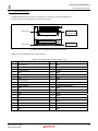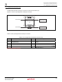
1
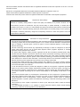
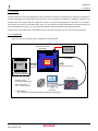
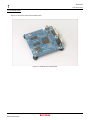
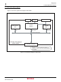
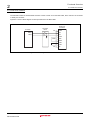
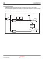
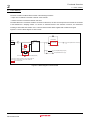
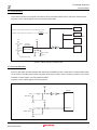
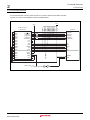
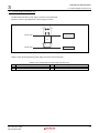
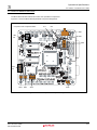
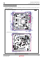
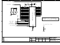
REJ11J0002-0100Z
SH7206 CPU Board
M3A-HS60
32
User's Manual
SuperH
Rev. 1.00
Issued:June 1,2005
TM
Renesas32-Bit RISC Microcomputers
RISC Engine Family/SH7200 Series/SH7206 Group
Microsoft, MS-DOS, Windows and Windows.NET are registered trademarks of Microsoft Corporation of the U.S. in the U.S.
and other countries.
IBM and AT are registered trademarks of International Business Machines Corporation of the U.S.
Adobe and Acrobat are registered trademarks of Adobe Systems Incorporated.
All other brand names and product names are registered trademarks or trademarks of the respective proprietors.
Requests for Safety Design
• Renesas is constantly making efforts to improve the quality and reliability of its products. However, not all
semiconductor products are trouble-free, they may become faulty or operate erratically. To ensure that no
accidents such as injury or a fire or no social damage may arise from Renesas semiconductor products should
they become faulty or operate erratically, please pay careful attention to the safety design of your system by,
for example, considering redundancy design and incorporating measures to check the spread of a fire and
prevent device malfunction.
Precautions on Using This Manual
• This manual only provides reference information to help customers purchase the appropriate type of Renesas
Technology product that suits the intended purpose of use, and the technical information contained herein
does not implicitly or otherwise grant a license or rights to use the intellectual property or other rights of
Renesas Technology.
• Renesas Technology will not assume any responsibility for damage or losses or infringement on the third
parties’ rights arising from the use of product data, diagrams, tables, programs, algorithms or example
application circuits presented in this manual.
• The product data, diagrams, tables, programs, algorithms and all other information presented herein reflect
the latest that was available at the time this manual was issued, and Renesas Technology reserves the right
to change the products or specifications described herein without prior notice. When purchasing Renesas
Technology semiconductor products, please contact Renesas Technology or Renesas Technology Sales or
other distributors to obtain the latest information, and also keep abreast of the information published at the
Renesas Technology home page (http://www.renesas.com) or through other media.
• The information contained herein was carefully prepared and is believed to be correct. However, Renesas
Technology will not assume responsibility for losses that the customers by any possibility may suffer because
of erroneous description in this manual.
• To use the technical contents in product data, diagrams or tables or the programs or algorithms presented
herein for your system, please carefully evaluate their suitability as part of the entire system, not singly as a
technical content, program or algorithm alone, to determine in advance whether they are actually suitable for
your system. Renesas Technology will not assume responsibility for the suitability of said items in user
systems.
• The products presented herein are not designed or manufactured for use in equipment or systems that are
used under conditions where human life is concerned. If you plan to use the products presented herein for
special applications such as transportation, mobile, medical, aerospace, nuclear control or submarine
repeater equipment or systems, please consult Renesas Technology or Renesas Technology Sales or other
distributors.
• This manual may not be copied or reproduced, in whole or part, without prior written consent of Renesas
Technology.
• For more detailed information or for questions or doubts about this manual, please consult Renesas
Technology or Renesas Technology Sales or other distributors.
Revision History
Rev.
SH7206 CPU Board M3A-HS60User's Manual
Date of Issue
Content of Revision
Page
1.00
June 1.2005
-
Points
First edition issued.
Table of Contents
Chapter1 Overview .............................................................................................................................. 1-1
1.1 Overview .................................................................................................................................................................... 1-2
1.2 Configuration .............................................................................................................................................................. 1-2
1.3 External Specifications ............................................................................................................................................... 1-3
1.4 External View ............................................................................................................................................................. 1-4
1.5 M3A-HS60 Block Diagram.......................................................................................................................................... 1-5
1.6 M3A-HS60 Board Overview ....................................................................................................................................... 1-6
1.7 M3A-HS60 Memory Mapping ..................................................................................................................................... 1-8
1.8 Absolute Maximum Ratings........................................................................................................................................ 1-9
1.9 Recommended Operating Conditions ........................................................................................................................ 1-9
Chapter2 Functional Overview ............................................................................................................ 2-1
2.1 Functional Overview................................................................................................................................................... 2-2
2.2 CPU............................................................................................................................................................................ 2-3
2.2.1 SH7206 ............................................................................................................................................................. 2-3
2.3 Memory ...................................................................................................................................................................... 2-4
2.3.1 SH7206's Internal RAM..................................................................................................................................... 2-4
2.3.2 Flash Memory M5M29KT331AVP (included as standard equipment) ............................................................... 2-4
2.3.3 External SDRAM ............................................................................................................................................... 2-6
2.4 Serial Port Interface.................................................................................................................................................... 2-9
2.5 I/O Ports ................................................................................................................................................................... 2-10
2.6 Power Supply Circuit ................................................................................................................................................ 2-12
2.7 Clock Module............................................................................................................................................................ 2-13
2.8 Reset Module ........................................................................................................................................................... 2-14
2.9 Interrupt Switches..................................................................................................................................................... 2-14
2.10 E10A-USB Interface ............................................................................................................................................... 2-15
Chapter3 Operational Specifications ................................................................................................... 3-1
3.1 M3A-HS60 Connectors Outline .................................................................................................................................. 3-2
3.1.1 H-UDI Connector (J1) ....................................................................................................................................... 3-3
3.1.2 Serial Port Connector (J2)................................................................................................................................. 3-4
3.1.3 External Power Supply Connectors(J3 and J5)................................................................................................. 3-5
3.1.4 Power Supply Connector (J4) ........................................................................................................................... 3-6
3.1.5 User I/O Connectors (J6-J8) ............................................................................................................................. 3-7
3.1.6 Extension Connectors (J9-J13) ......................................................................................................................... 3-9
3.2 Outline of Switches and LEDs .................................................................................................................................. 3-13
3.2.1 Power Supply Select Jumpers (JP1 and JP2)................................................................................................. 3-14
3.2.2 Switch and LED Functions .............................................................................................................................. 3-15
3.3 Outline Dimensions of M3A-HS60............................................................................................................................ 3-17
Appendix .............................................................................................................................................A-1
M3A-HS60 Schematics
Rev. 1.00 June 1,2005
REJ11J0002-0100Z
(i)
Chapter1Overview
Chapter1
Overview
1-1
Overview
1
1.1 Overview
1.1 Overview
The M3A-HS60 is the CPU board designed for users to evaluate the function and performance of original microcomputers of
Renesas Technology the SH7206 series. With the board, you can develop and evaluate the application software for the
SH7206 series. The SH7206's data bus, address bus, and pins of various internal peripheral circuit function are connected to
the extension bus connector of the M3A-HS60. Thus, you can evaluate the timing relationships with peripheral devices by
using measurement instruments. You can also develop extension boards depending on development purposes.
Furthermore, the E10A-USB, the on-chip emulator made by Renesas Technology, can be connected to the M3A-HS60.
1.2 Configuration
Figure1.2.1 shows an example system configuration using M3A-HS60.
SH7206 CPU Board
M3A-HS60
Power supply
(5V/1.5A or more)
*1
H-UDI/AUD
SH7206
Application
Board
Extension
connector
Serial port connector
* Created according to
the intended application
HEW
debugger
High-performance *1
E10A-USB *1
Embeded Workshop(HEW)
SuperH RISC engine *1
C/C++ compiler package
USB
*1
Host
Computer
*1: Option Items:
It is necessary to prepare separately for software development.
Figure1.2.1 Example System Configuration of M3A-HS60
Rev.1.00 June 1,2005
REJ11J0002-0100Z
1-2
Overview
1
1.3 External Specifications
1.3 External Specifications
Table1.3.1 lists external specifications of M3A-HS60
Table1.3.1 External Specifications of M3A-HS60
No.
Item
Content
SH7206(R5S72060)
1
CPU
z Input(XIN)clock: 16.67MHz
z Bus clock: 66.67MHz,max
z CPU clock: 200MHz,max
Following items of memory are included.
zSDRAM: 32 Mbytes, max.
Following memory selectable by a DIP switch.
• When 16-bit bus width is selected
2
Memory
EDS1216AATA-75E x 1: 16 Mbytes
• When 32-bit bus width is selected
EDS1216AATA-75E x 2: 32 Mbytes
z Flash memory
• M5M29KT331AVP x 1: 4Mbytes
• Data bus width fixed to 16 bits
z Extension connector (bus, I/O, VCC, GND: 100 pins)
3
Connectors
z User I/O connector (SH7206's MTU2 and A/D function pins: 32 pins)
z Serial port connector (D-sub 9 pins)
z H-UDI connector (36 pins)
4
LED
z POWER LED (1 pc.)
z User LED(7 pcs.)
z Reset switch (1 pc.)
z MRES switch (1 pc.)
5
Switches
z NMI switch (1 pc.)
z User DIP switch (1 pc., 4 poles)
z System setup DIP switch (1 pc., 5 poles)
z Dimensions: 100 mm x 100 mm
6
Package Dimensions
z Mounting form: 4-layer, double-side mounted
z Board configuration: 1 board
Rev.1.00 June 1,2005
REJ11J0002-0100Z
1-3
Overview
1
1.4 External View
1.4 External View
Figure1.4.1 shows the external view of M3A-HS60.
Figure1.4.1 External View of M3A-HS60
Rev.1.00 June 1,2005
REJ11J0002-0100Z
1-4
Overview
1
1.5 M3A-HS60 Block Diagram
1.5 M3A-HS60 Block Diagram
Figure1.5.1 shows the system block diagram of M3A-HS60.
H-UDI
Serial port
connector
SH7206
200MHz
Flash memory
4MB
16 or 32
16
User I/O Connector
SDRAM
16MB x 2
16 or 32
External:66.67MHz
SH7206 CPU Board
M3A-HS60
Extension connector
Enables to connect extension boards, or
enables to monitor all of bus and peripheral
I/O signals.
Figure1.5.1 System Block Diagram of M3A-HS60
Rev.1.00 June 1,2005
REJ11J0002-0100Z
1-5
Overview
1
1.6 M3A-HS60 Board Overview
1.6 M3A-HS60 Board Overview
Figure1.6.1 shows the M3A-HS60 board overview.
J4
Top view of the
Component side
Power
Supply
Connector
JP1,JP2
Power Supply
Select Jumper
LED6-8
User LED
SW1
Power
Switch
LED1
Power LED
SW4
System setup
DIP switch
SDRAM
(16MB)
U5
J1
H-UDI Connector
(36-pin)
U1
J6
J7
SH7206
U8 SDRAM
(16MB)
LED2-5
U3
User
LED
J2
Flash
Memory
Serial Port
Connector
SW2
Reset
Switch
J3
SW5
SW3
U2
Clock
NMI
User
Switch DIP Switch Buffer
J5
U9
X1
SW6
Oscillator RS-232C MRES
16.67MHz
Driver
Switch
(not mounted)
Top view of the
Solder side
J12
U10
J13
3.3V Power
Regulator
J6
U12
1.25V Power
Regulator
U4
Address Shift
Buffer
U7
J11
U6
Logic IC(LVC14)
J9
U11
Reset IC
J10
:Extension connector(not mounted)
Figure1.6.1 M3A-HS60 Board Overview
Rev.1.00 June 1,2005
REJ11J0002-0100Z
1-6
Overview
1
1.6 M3A-HS60 Board Overview
Table1.6.1 lists main components mounted in M3A-HS60.
Table1.6.1 Main Components Mounted in M3A-HS60
Recommended parts’
Symbol
Component name
Note
number for not mounted
components (Makers)
U1
CPU
SH7206 (by Renesas)
U2
Clock Buffer
Not mounted
U3
Flash Memory
M5M29KT331AVP
CY2305SC-1 (by Cypress)
(by Renesas)
U4,U7
Address Shift Buffer
U5,U8
SDRAM
U6
Logic IC
U9
RS-232C Driver
U10
3.3V Power Regulator
U11
Reset IC
U12
1.25V Power Regulator
X1
16.67MHz Oscillator
16.67MHz
X2
Ceramic Resonators
Not mounted, 16.67MHz
EDS1216AATA-75
M51957BFP (by Renesas)
CSTCE-G16M67
(by Murata)
J1
H-UDI Connector
J2
Serial port Connector
J3,J5
External Power Supply Connector
Not mounted
A2-2PA-2.54DSA
(by Hirose)
J4
Power Supply Connector
J6
Extension connector
Not mounted,
XG4C-2634 Right angle
26pin MIL Standard Connector
J7, J8
Extension connector
Not mounted,
A2-3PA-2.54DSA
3pin MIL Standard Connector
J9, J11, J13
Extension connector
Not mounted,
XG4C-2031
20pin MIL Standard Connector
J10, J12
Extension connector
Not mounted,
XG4C-4031
40pin MIL Standard Connector
LED1
Power LED
Red
LED2-8
User LED
Green
SW1
Power Switch
SW2
Reset Switch
SW5
NMI Switch
SW6
MRES Switch
SW3
User DIP Switch
SW4
System setup DIP Switch
Rev.1.00 June 1,2005
REJ11J0002-0100Z
1-7
Overview
1
1.7 M3A-HS60 Memory Mapping
1.7 M3A-HS60 Memory Mapping
Figure1.7.1 shows the memory mapping example of SH7206 in the M3A-HS60.
Logical address
H'0000 0000
H'003F FFFF
Logical space of theSH7206
CS0 space:64MB
Memory Mapping of theM3A-HS60
Flash Memory(4MB)
16-bit bus
User area
H'0400 0000
CS1 space:64MB
User area
CS2 space:64MB
User area
H'0800 0000
H'0C00 0000
CS3 space:64MB
H'0CFF FFFF
SDRAM(32MB)
32-bit bus
SDRAM(16MB)
16-bit bus
User area
H'0DFF FFFF
User area
H'1000 0000
CS4 space:64MB
User area
CS5 space:64MB
User area
CS6 space:64MB
Reserved area
(Disabled)
CS7 space:64MB
Reserved area
(Disabled)
CS0-CS7 spaces
(non-cacheable area)
CS0-CS7 spaces
(non-cacheable area)
CS8 space:1GB
User area
Reserved area
(Disabled)
Reserved area
(Disabled)
Internal RAM(128KB)
Internal RAM(128KB)
Internal RAM, Reserved
Internal RAM, Reserved
Internal peripheral module
Internal peripheral module
H'1400 0000
H'1800 0000
H'1C00 0000
H'2000 0000
H'4000 0000
H'8000 0000
H'FFF8 0000
H'FFFA 0000
H'FFFC 0000
H'FFFF FFFF
Note: There is the cacheable area from H’0000 0000~H’1FFF FFFF.
Figure1.7.1 Memory Mapping Example of SH7206
Rev.1.00 June 1,2005
REJ11J0002-0100Z
1-8
Overview
1
1.8 Absolute Maximum Ratings
1.8 Absolute Maximum Ratings
Table1.8.1 lists the absolute maximum ratings of M3A-HS60.
Table1.8.1 Absolute Maximum Ratings of M3A-HS60
Symbol
Parameter
Rated Value
Remarks
VCC
5V System Power Supply Voltage
-0.3V to 6.0V
Relative to VSS
3VCC
3.3V System Power Supply Voltage
-0.3V to 4.6V
Relative to VSS
1.2VCC
1.25V System Power Supply Voltage
-0.3V to 1.7V
Relative to VSS
Operating Ambient Temperature
-5°C to 55°C
No dewdrops allowed.
Topr
Use in corrosive gas environment prohibited.
Tstr
Storage Ambient Temperature
-10°C to 60°C
No dewdrops allowed.
Use in corrosive gas environment prohibited.
Note: The ambient temperature refers to the air temperature in the closest place from the board.
1.9 Recommended Operating Conditions
Table1.9.1 lists the recommended operating conditions of the M3A-HS60.
Table1.9.1 Recommended Operating Conditions of M3A-HS60
Symbol
Parameter
VCC
5V System Power Supply Voltage
3VCC
3.3V System Power Supply Voltage
Rated Value
Remarks
4.75V to 5.25V
Relative to VSS
3.0V to 3.6V
Relative to VSS
(Normally supplied from regulator)
1.2VCC
1.25V System Power Supply Voltage
1.15V to 1.35V
Relative to VSS
(Normally supplied from regulator)
–
Topr
Maximum Power Consumption in the Board
Operating Ambient Temperature
Within 1A
5°C to 50°C
No dewdrops allowed.
Use in corrosive gas environment prohibited.
Rev.1.00 June 1,2005
REJ11J0002-0100Z
1-9
Overview
1
1.8 Absolute Maximum Ratings
This is a blank page
Rev.1.00 June 1,2005
REJ11J0002-0100Z
1-10
Chapter2Functional Overview
Chapter2
Functional Overview
2-1
Functional Overview
2
2.1 Functional Overview
2.1 Functional Overview
Table2.1.1 lists the functional modules of M3A-HS60.
Table2.1.1 Functional Modules of M3A-HS60
Sections
2.2
Function
CPU
Content
SH7206
zInput(XIN)clock : 16.67MHz
zBus clock : 66.67MHz,max
zCPU clock : 200MHz,max
2.3
Memory
Following items of memory are included
z SDRAM: 32 Mbytes, max
By switching a DIP switch, the following memories can be selected.
• When 16-bit bus width is selected
EDS1216AATA-75E x 1: 16 Mbytes
• When 32-bit bus width is selected
EDS1216AATA-75E x 2: 32 Mbytes
z Flash memory
• M5M29KT331AVP x 1: 4 Mbytes
• Data bus width fixed to 16 bits
2.4
Serial port interface
Connects SCIF0 of the SH7206 to the Serial port connector.
2.5
I/O ports
Connects to the I/O ports of the SH7206
2.6
Power Supply Circuit
Controls the system power supply of the M3A-HS60
2.7
Clock Module
Controls the clock
2.8
Reset Module
Controls device reset mounted on the M3A-HS60
2.9
Interrupt switches
Connects to NMI and MRES pins
2.10
E10A-USB Interface
SH7206 H-UDI/AUD interface
Operational specifications
Connectors, switches and LEDs
–
z SH7206 extension connector
z Switches and LEDs
z H-UDI connector
Detailed in Chapter 3.
Rev.1.00 June 1,2005
REJ11J0002-0100Z
2-2
Functional Overview
2
2.2 CPU
2.2 CPU
2.2.1 SH7206
The M3A-HS60 contains SH7206, the 32-bit RISC microcomputer, which operates with a maximum 200MHz of CPU
clock frequency. The SH7206 includes 128-Kbyte RAM, 8-Kbyte instruction cache and 8-Kbyte data cache, and it can
deal with a wide range of applications from data processing to equipment control.
The M3A-HS60 can be operated with a maximum 200MHz of CPU clock frequency (external bus 66.67MHz, max.)
using a 16.67MHz input clock.
Figure2.2.1 shows the block diagram of SH7206 in the M3A-HS60.
SH7206
Mode
3.3V
GND
GND
System
Control
Address bus
23
Data bus
16
Bus control
WAIT#/DACK2/PA17
RD#
WE0#/DQMLL/#POE6/PA12
WE1#/WE#/DQMLU#/POE7#/PA13
CS0 space
MD2
WE2#/ICIORD#/DQMUL#/TIC5V/PA22
Fixed 16-bit bus WE3#/ICIOWR#/AH#/DQMUU#/TIC5W/PA23
MD0
Mode 2
MD_CLK2
RD_WR#/IRQ2/TCLKC/PA8
MD_CLK0
FRAME#/CKE/TCLKD/IRQ3/PA9
RASL#IRQ2/#POE2/PB4
RES#
CASL#/IRQ3/POE3#PB5
MRES#/TIOC4B/PE13
BS#/RXD2/TIOC2B/UBCTRG/PE7
WDTOVF#
SCK2/TIOC3A/PE8
BREQ#/TEND0/PINT2/PA18
IRQ1/POE1/SDA/PB3
BACK#/TEND1/PINT3/PA19
IRQ0/POE0#/SCL/PB2
TXD2/TIOC3C/PE10
A25/DREQ0/IRQ0/SCK0/PA2
TEND0/TIOC0B/PE1
A24/RXD1/PA3
DREQ1/TIOC0C/PE2
A23-A1
SCK3/TIOC3B/RTS3#/PE9
A0/PC0
TXD3/TIOC4A/PE12
D31/TIOC3AS/ADTRG#/PD31
RXD3/TIOC3D/CTS3#
D30/TIOC3CS/IRQOUT#PD30
DACK1//CKE/TIOC4D/IRQOUT#/PE15
D29/CS3#/TIOC3BS/PD29
WE3#/ICIOWR#/AH#/DACK0/TIOC4C/PE14
D28/CS2#/TIOC3DS/PD28
NMI#
D27/DACK1/TIOCS4AS/PD27
AUDATA0-3
D26/DACK0/TIOC4BS/PD26
TCK
D25/DREQ1/TIOC4CS/PD25
TMS
D24/DREQ0/TIOC4DS/PD24
TDI
D23/IRQ7/PD23
TDO
D22/IRQ6/TIC5US/PD22
TRST#
D21/IRQ5/TIC5VS/PD21
ASEBRKAK#/ASEBRK#
D20/IRQ4/TIC5WS/PD20
AUDCK
D19/IRQ3/POE7#/PD19
AUDSYNC#
D18/IRQ2/POE6#/PD18
ASEMD#
D17/IRQ1/POE5#/PD17
ASEBCK
D16/IRQ0/POE4#/PD16
ASEBRK#
D15-0
TXD0
CS0#
RXD0
CS1#/POE5#/PA11
EXTAL
XTAL
CKIO
Clock
CS2#/TCLKA/PA6
CS3#/TCLKB/PA7
CS4#/RASU#/PINT4/PA20
CS5#/CE1A#/CASU#/PINT5/TIC5U/PA21
CS8#/PE16
CE2A#/DREQ3/PINT6/PA24
CE2B#/DACK3/PINT7/POE8#/PA25
AN0-AN5/PF0-PF5
AN6/DA0/PF6
AN7/DA1/PF7
Bus control
IRQ/SCI/IIC
DMAC/GPIO
MTU2
NMI
4
E10A-USB
Interface
Serial port
Interface
6
A/D Converter
D/A Converter
Figure2.2.1 Block Diagram of SH7206
Rev.1.00 June 1,2005
REJ11J0002-0100Z
2-3
Functional Overview
2
2.3 Memory
2.3 Memory
The M3A-HS60 includes the internal RAM of the SH7206 (128 Kbytes), external Flash memory, and external SDRAM.
These memory chips are detailed below.
2.3.1 SH7206's Internal RAM
The SH7206 contains an internal 128-Kbyte RAM.
2.3.2 Flash Memory M5M29KT331AVP (included as standard equipment)
The M3A-HS60 includes the Flash memory shown in Table2.3.1 as standard equipment. The memory can be used as
the storage in which to save the user program. The Flash memory to boot is fixed to 16-bit mode of external bus and
operates with a single 3.3 V power supply voltage. The write-protect of Flash memory can be enabled or disabled by
using a DIP switch.
Figure2.3.1 shows a block diagram of Flash memory.
Table2.3.2 lists bus state controller settings (write/read) for operation with the SH7206 bus clock at 66.67MHz.
Table2.3.1 Outline of the Flash Memory
Part Number
Bus Size
Capacity
Access Time
M5M29KT331AVP
16-bit mode
4 Mbytes(16 bits × 2 Mword × 1pc.)
70ns
M5M29KT331AVP
(2 M Word x16 bit)
SH7206
A20
A21
20
A20-A1
A19-A0
16
D15-D0
DQ15-DQ0
3.3 V
BYTE#
RD#
OE#
WE0#
WE#
CS0#
CE#
RP#
RES#
NC
3.3 V
RY/BY#
WP#
DIP SW
Figure2.3.1 Block Diagram of Flash Memory
Rev.1.00 June 1,2005
REJ11J0002-0100Z
2-4
Functional Overview
2
2.3.2 Flash Memory M5M29KT331AVP (included as standard equipment)
Table2.3.2 Examples for Bus State Controller Settings (Flash Memory Write/Read)
User Area
Applicable Device
CS0
Bus State Controller Settings
M5M29KT331AVP
CS0 Space Bus Control Register : CS0BCR
Initial value : H'36DB 0600(when MD2= H and MD0=L)
Recommended set value : H'1000 0400
• Specify idle state in write to read and write to write intervals
IWW[2:0] = B'001: 1 idle cycles inserted
• Specify data bus
BSZ[1:0] = B'10 : 16-bit bus width
CS0 Space Wait Control Register (CS0WCR)
Initial value: H'0000 0500
Recommended set value : H'0000 0AC1
• Address, CS0# assert -> RD#, WEn# assert delay cycle
SW[1:0] = B'01 : 1.5 cycles
• Specify access wait cycles
WR[3:0] = B'0110 : 5 cycles
• RD#, WEn# negate -> Address, CS0 negate delay cycle
HW[1:0] = B'01 : 1.5 cycles
<Write and Read Timing>
Write1
Th
T1
Write2
Tw1 Tw2 Tw3 Tw4 Tw5
T2
Tf
Taw1
Th
T1
Tw1 Tw2 Tw3 Tw4 Tw5
Read1
T2
Tf
Taw1
Th
T1
Tw1 Tw2 Tw3 Tw4 Tw5
T2
Tf
CKIO
tWC
tAD1
tAD1
tAD1
tCSD1
tCSD1
tAD1
tAD1
tAD1
tRC
A21-A1
tCSD1
tCSD1
tCSD1
tCSD1
CS0#
tRSD
tRSD
RD#
tWED1
tWED1
tWPH
tCS
tWP
tAS
tWED1
tAH
tCH
tWED1
tOEH
tWP
tAS
tCH
tAH
WE0#
tDS
tWDD1
D15-D0
DATA
tDS
tWDH1
tDH
tWDD1
tWDH1
tDH
ta(OE)
ta(AD)
ta(CE1)
DATA
tRDS1
DATA
tRDH1
tDF(OE)
Figure2.3.2 Flash Memory Read and Write Access Timing
Rev.1.00 June 1,2005
REJ11J0002-0100Z
2-5
Functional Overview
2
2.3.3 External SDRAM
2.3.3 External SDRAM
The M3A-HS60 includes two pcs. of 16-Mbyte SDRAM (for an external SDRAM) as standard equipment.
The SH7206's internal bus state controller can be used to control the SDRAM.
Note that the SDRAM can be switched between 32-bit bus access and 16-bit bus access. (For 16-bit bus access, only
one pc. of 16-Mbyte SDRAM can be used.)
Table2.3.3 lists SDRAM specifications used in M3A-HS60. Figure2.3.3 shows a block diagram of SDRAM.
Table2.3.3 SDRAM Specifications Used in M3A-HS60
Specification
Content
Part number
EDS1216AATA-75E
Configuration
16 Mbytes (16-bit bus width) x 2pcs.
Capacity
32 Mbytes
Access time
5.4ns
CAS latency
2 (At 66MHz bus clock)
Refresh interval
4,096 refresh cycles every 64ms
Row address
A11- A0
Column address
A8 - A0
Number of banks
4-bank operation controlled by BA0 and BA1
3.3V
SDRAM
bus size setting
SDRAM_SZ
SH7206
A15-1
14
3.3V
SDRAM_SZ=Low:16-bit access using SDRAMx1
SDRAM_SZ=High:32-bit access using SDRAMx2
32-bit Access
A[13:2], A15-14
EDS1216AATA
(8Mx16 bits)
14
MA11-0,BA1-0
CS#
CS3#
DQ15-DQ0
16
SH72060 D31-D16
1OE#
2OE#
DQMUU
DQMUL
DQMU
DQML
CLK
CKIO
CKE
CKE
RD/WR#
WE#
RASL#
RAS#
CASL#
CAS#
16-bit Access
A[12:1], A14-13
EDS1216AATA
(8Mx16 bits)
14
MA11-0,BA1-0
CS#
DQ15-DQ0
16
SH72060 D15-D0
1OE#
2OE#
DQMLU
DQMU
DQMLL
DQML
CLK
CKE
WE#
RAS#
CAS#
Figure2.3.3 Block Diagram of External SDRAM
Rev.1.00 June 1,2005
REJ11J0002-0100Z
2-6
Functional Overview
2
2.3.3 External SDRAM
Table2.3.4 lists bus state controller settings for operation with the SH7206 Bus clock at 66.67MHz.
Table2.3.4 Examples for Bus State Controller Settings (SDRAM Read/ Write)
User Area
CS3
Rev.1.00 June 1,2005
REJ11J0002-0100Z
Application Device
EDS1216AATA-75E
Bus State Controller Settings
CS3 Space Bus Control Register (CS3BCR)
Initial value: H'36DB 0600
Recommended set value: H'0000 4400 (for 16-bit bus) or H'0000 4600
(for 32-bit bus)
• Specify memory
TYPE[2:0] B'100; SDRAM
• Specify data bus
BSZ[1:0] = B'10; 16-bit bus width
BSZ[1:0] = B'11; 32-bit bus width
CS3 Space Wait Control Register (CS3WCR)
Initial value: H'0000 0500, Recommended set value: H'0000 2892
• Precharge completion wait cycles
WTRP[1:0] = B'01; 1 cycles
• Wait cycles between ACTV command -> READ(A)/WRITE(A)command
WTRCD[1:0] = B'10; 2 cycles
• Area 3 CAS latency
A3CL[1:0] = B'01; 2 cycles
• Precharge start wait cycles
TRWL[1:0] = B'10; 2 cycles
• Idle cycles between REF command/self-refresh deactivation
-> ACTV/REF/MRS command
WTRC[1:0] = B'10; 5 cycles
SDRAM Control Register (SDCR)
Initial value: H'0000 0000, Recommended set value: H'0000 0809
• Refresh control
RFSH = B'1; Refresh enabled
• Refresh control
RMODE = B'0; Auto refresh
• Bank active mode
BACTV = 0; Auto precharge mode
• Area 3 row address bits
A3ROW[1:0] = B'01; 12 bits
• Area 3 column address bits
A3COL[1:0] = B'01; 9 bits
Refresh Timer Control/Status Register (RTCSR)
Initial value: H'0000 0000, Recommended set value: H'A55A 0010
• Clock select
CKS[2:0] = B'010; B-φ/16
• Refresh times
RRC[2:0] = B'000; 1 time
Refresh Time Constant Register (RTCOR)
Initial value: H'0000 0000, Recommended set value: H'A55A 0041
* The following shows refresh request intervals in cases when clock
select is set to B- φ/16.
1 cycle: 240ns (66MHz/16 = 4.125MHz)
Refresh request intervals for the SDRAM: every 15.625µs
15.625µs/240ns = 64 (0x41) cycles per refresh
AC Characteristics Switching Register (ACSWR)
Initial value: H'0000 0000, Recommended set value: H'0000 0009
• AC Characteristics Switch
ACOSW[3:0] = B'1001; Switches characteristics and extends the
delay time
2-7
Functional Overview
2
2.3.3 External SDRAM
SDRAM SINGLE READ
SDRAM SINGLE WRITE
tRC
tRC
tRAS
tRP
tRAS
tRP
tRCD
tDPL
tDAL
ACT
Tr
Trw1
Trw2
READA
Tc1
Tcw
Td1
Tde
Tap
ACT
Tr
Trw1
Trw2
WRITEA
Tc1
Trw11
Trw12
Tap
ACT
Tr
CKIO
CKE
tSI
tSI
tHI
tCSD1
tHI
tCSD1
tCSD1
tCSD1
CS3#
tRASD1
tHI
tSI
tRASD1
tRASD1
tRASD1
RASL#
tHI
tSI
tCASD1
tCASD1
tCASD1
tCASD1
CASL#
tRWD1
tRWD1
RD/WR#
tDQMD1
tDQMD1
tDQMD1
tDQMD1
DQMUU-LL
tAD1
tAD1
tAD1
tAD1
tAD1
tAD1
tAD1
tAD1
tAD1
tAD1
tAD1
tAD1
tAD1
tAD1
tAD1
tAD1
tAD1
tAD1
A11-A2(A9-A0)
A12(A10/AP)
A15,A14(BA1,0)
tLZ
D0-31
tAC
Data
tRDS2
tRDH2
tOH
tOHZ
tHI
tSI
tWDD2
tWDH2
Figure2.3.4 Typical SDRAM Single Read/Write Timing
Rev.1.00 June 1,2005
REJ11J0002-0100Z
2-8
Functional Overview
2
2.4 Serial Port Interface
2.4 Serial Port Interface
The SH7206 included in the M3A-HS60 contains a UART module. As for the M3A-HS60, SCIF channel 0 is connected
to serial port connector.
Figure2.4.1 shows a block diagram of serial port interface in the M3A-HS60.
SH7206
RXD0
TXD0
RS-232C
driver
Serial port
connector
NC 1
2
3
4
GND 5
6
DCD#
RxD
TxD
DTR#
GND
DSR#
7
RTS#
8
CTS#
NC 9
RI#
Figure2.4.1 Block Diagram of Serial Port Interface
Rev.1.00 June 1,2005
REJ11J0002-0100Z
2-9
Functional Overview
2
2.5 I/O Ports
2.5 I/O Ports
As for the M3A-HS60, the SH7206's I/O ports are connected to the extension bus connector of the M3A-HS60 board.
Some I/O ports are connected to DIP switches and LEDs of the M3A-HS60 board. Users are free to use these ports.
Figure2.5.1 shows a block diagram of SH7206 I/O ports.
Table2.5.1 shows the functions of SH7206 I/O ports.
3.3V
LED8
GREEN
LED7
GREEN
LED6
GREEN
LED5
GREEN
LED4
GREEN
LED3
GREEN
LED2
GREEN
SH7206
PE1
PE2
PE8
PE10
PE11
PE14
PE15
3.3V
DIP Switch
SW3-1
SW3-2
PA18
PA19
SW3-3
PA24
SW3-4
PA25
Figure2.5.1 Block Diagram of SH7206 I/O Ports
Rev.1.00 June 1,2005
REJ11J0002-0100Z
2-10
Functional Overview
2
2.5 I/O Ports
Table2.5.1 Functions of SH7206 I/O Ports
SH7206 Port Name
Connection in the M3A-HS60
PA0-PA1
Serial port connector.
PA2
Extension connector, SDRAM_SZ signal input.
PA3,PA6,PA11,PA17,
Extension connector.
PA20,PA21
PA4-PA5
Flash memory and extension connector.
PA7-PA9,PA13,PA22,PA23
SDRAM and extension connector.
PA12
Flash memory, SDRAM and extension connector.
PA13
SDRAM and extension connector.
PA18
SW1-1 and extension connector.
PA19
SW1-2 and extension connector.
PA24
SW1-3 and extension connector.
PA25
SW1-4 and extension connector.
PB2,PB3
Extension connector.
PB4,PB5
SDRAM and extension connector.
PB9
Flash memory and extension connector.
PC0
Extension connector.
PC1
Flash memory, SDRAM and extension connector.
PD8-PD15
Flash memory, SDRAM and extension connector.
PD16-PD31
SDRAM (when 32-bit bus selected) and extension connector.
PE1
LED2 and extension connector.
PE2
LED3 and extension connector.
PE7,PE9,PE12,PE13,PE16
Extension connector.
PE8
LED4 and extension connector.
PE10
LED5 and extension connector.
PE11
LED6 and extension connector.
PE14
LED7 and extension connector.
PE15
LED8 and extension connector.
PF0-7
Extension connector.
Rev.1.00 June 1,2005
REJ11J0002-0100Z
2-11
Functional Overview
2
2.6 Power Supply Circuit
2.6 Power Supply Circuit
The M3A-HS60 accepts a 5V power supply as its input, and generates 3.3V and 1.25V by using a regulator.
The regulator used here is an output voltage variable type, so that any desired voltage can be generated by changing
the resistance value.
Figure2.6.1 shows a block diagram of power supply circuit in the M3A-HS60.
Extension connector
Extension connector
SW1
SDRAM
5V
Flash
memory
5V ->
3.3V
3
1
External
power supply J3
JP1
2
SH7206
2
JP2
5V ->
1.25V
3
External
power supply J5
1
Figure2.6.1 Block Diagram of Power Supply Circuit
Rev.1.00 June 1,2005
REJ11J0002-0100Z
2-12
Functional Overview
2
2.7 Clock Module
2.7 Clock Module
The clock module in the M3A-HS60 consists of the following two blocks:
• Output from a oscillator connected to EXTAL of the SH7206
• Ceramic resonator connected to EXTAL and XTAL
The M3A-HS60 has a 16.67MHz oscillator connected. Furthermore, the bus clock output from the SH7206 is connected
to the SDRAM via a damping resistor. To connect an extension board to the extension connector, we recommend
including a clock buffer that contains a PLL to ensure that the board will be supplied with a stable clock signal.
Figure2.7.1 shows a block diagram of clock module.
R14
Oscillator
SH7206
Clock Buffer
R18
EXTAL
CLK
CKIO
XTAL
R82
Not mounted
EXCLK(Extension connector)
*2
CY2305SC-1H(Cypress)
Ceramic
Resonator
CLKIH(SDRAM upper bytes)
CLKIL(SDRAM lower bytes)
*1
Not mounted
CSTCE-G16M67(Murata)
*1:To mount ceramic resonator, remove the resistor 18
*2:To mount a clock buffer, remove the resistor 14
:Not mounted parts
Figure2.7.1 Block Diagram of Clock Module
Rev.1.00 June 1,2005
REJ11J0002-0100Z
2-13
Functional Overview
2
2.8 Reset Module
2.8 Reset Module
This module controls the reset signals connected to both the SH7206 and Flash memory mounted in the M3A-HS60.
Figure2.8.1 shows a block diagram of the reset module in M3A-HS60.
H-UDI connector
RES#
ResetIC output delay time,td=0.34 x Cd(pF)µsec = 34ms
ResetIC output detection voltage,Vs = 1.25 x
Flash memory
= 2.5V
) Ra+Rb
Rb )
RP#
Extension connector
Ra
10KW
Reset IC
M51957BFP
Input
Rb
10KW
RESET#
3.3V
3.3V
SH7206
*
Output
RES#
Delay capacitance
Cd
0.1µF
Reset switch
SW 2
*Open-collector output
Figure2.8.1 Block Diagram of Reset Module
2.9 Interrupt Switches
As for the M3A-HS60, both the SH7206's NMI interrupt pin and MRES pin have a push switch connected. MRES switch
can be used for controlling manual reset for SH7206. When manual reset is done, the internal condition of CPU will be
formatted, but each register of on-chip peripheral module.
Figure2.9.1 shows a block diagram of interrupt switches.
3.3V
SH7206
NMI#
SW 5
NMI switch
3.3V
SW 6
MRES#/PE13
MRES switch
Figure2.9.1 Block Diagram of Interrupt Switches
Rev.1.00 June 1,2005
REJ11J0002-0100Z
2-14
Functional Overview
2
2.10 E10A-USB
2.10 E10A-USB Interface
As for the M3A-HS60, a 36-pin H-UDI connector to connect it with the E10A-USB is mounted.
Figure2.10.1 shows a block diagram of the E10A-USB interface.
3.3V
3.3V
H-UDI connector
(36-pin type)
2
4
6
8
10
12
14
16
18
20
22
24
26
28
30
GND
GND
GND
GND
GND
GND
GND
GND
GND
SH7206
AUDCK
AUDATA0
AUDATA1
AUDATA2
AUDATA3
AUDSYNC#
N.C.
N.C.
TCK
TMS
GND
TRST#
(GND)
GND
TDI
TDO
GND
GND ASEBRKAK#/ASEBRK#
UVCC
GND
32
RES#
GND
34
GND
GND
36
GND
N.C.
1
3
5
7
9
11
13
15
17
19
21
23
25
27
29
31
33
35
AUDCK
AUDATA0
AUDATA1
AUDATA2
AUDATA3
AUDSYNC#
TCK
TMS
TRST#
TDI
TDO
ASEBRKAK#/ASEBRK#
ASEMD#
RES#
Reset signal
Figure2.10.1 Block Diagram of the E10A-USB Interface
Rev.1.00 June 1,2005
REJ11J0002-0100Z
2-15
Functional Overview
2
2.10 E10A-USB
This is a blank page
Rev.1.00 June 1,2005
REJ11J0002-0100Z
2-16
Chapter3 Operational Specifications
Chapter3
Operational Specifications
3-1
Operational Specifications
3
3.1 M3A-HS60 Connectors Outline
3.1 M3A-HS60 Connectors Outline
Figure3.1.1 shows the M3A-HS60 connectors assignments.
<Top view of the component side>
J4
J1
J7, J8
J2
J3, J5
<Top view of the solder side>
J12
J13
J6
J11
J9
J10
Figure3.1.1 M3A-HS60 Connector Assignment
Rev.1.00 June 1,2005
REJ11J0002-0100Z
3-2
Operational Specifications
3
3.1.1 H-UDI Connector (J1)
3.1.1 H-UDI Connector (J1)
The M3A-HS60 includes an H-UDI (J1) connector for connection to the E10A-USB emulator.
Figure3.1.2 shows a pin arrangement of the H-UDI connector.
35
36
1
2
Board edge
Top view of the
Component side
J1
Board edge
Side view
Figure3.1.2 Pin Arrangements of the H-UDI Connector
Table3.1.1 lists pin assignments of H-UDI connector.
Table3.1.1 Pin Assignments of H-UDI Connector (J1)
Pin
Signal Name
Pin
Signal Name
1
AUDCK(PE0)
19
TMS
2
GND
20
GND
3
AUDATA0(PE6)
21
TRST#
GND
22
GND
AUDATA1(PE5)
23
TDI
GND
4
5
6
GND
24
7
AUDATA2(PE4)
25
TDO
8
GND
26
GND
9
AUDATA3(PE3)
27
ASEBRKAK#/ASEBRK#
10
GND
28
GND
11
AUDSYNC#(PA16)
29
+3.3V
GND
30
GND
NC
31
RES#
GND
12
13
14
GND
32
15
NC
33
GND
16
GND
34
GND
17
TCK
35
NC
18
GND
36
GND
Rev.1.00 June 1,2005
REJ11J0002-0100Z
3-3
Operational Specifications
3
3.1.2 Serial Port Connector (J2)
3.1.2 Serial Port Connector (J2)
The M3A-HS60 includes a serial port connector for serial communication (J2).
Figure3.1.3 shows a pin assignment of serial port connector.
5
9
1
6
Board edge
Top view of the
Component side
J2
5
9
1
6
Board edge
Side view
Figure3.1.3 Pin Arrangement of Serial Port Connector (J2)
Table3.1.2 lists pin assignments of serial port connector.
Table3.1.2 Pin Assignments of Serial Port Connector (J2)
Pin
Signal Name
Pin
Signal Name
1
NC
6
DSR#
2
RXD(PA0/RxD0)
7
RTS#
3
TXD(PA1/TxD0)
8
CTS#
4
DTR#
9
NC
5
GND
Pins 4-8 are loopback-connected.
Rev.1.00 June 1,2005
REJ11J0002-0100Z
3-4
Operational Specifications
3
3.1.3 External Power Supply Connectors(J3 and J5)
3.1.3 External Power Supply Connectors(J3 and J5)
The M3A-HS60 has the through-hole for two external power supply connectors (J3 for 3.3 V and J5 for 1.25 V) for the
SH7206.
Figure3.1.4 shows a pin assignment of external power supply connectors.
J3
J5
1 2
1 2
Top view of the
Component side
Board edge
Figure3.1.4 Pin Arrangement of External Power Supply Connectors (J3 and J5)
Table3.1.3, and Table3.1.4 list pin assignments of external power supply connectors.
Table3.1.3 Pin Assignments of External Power Supply Connector (J3)
Pin
1
Signal Name
+3.3V
Pin
2
Signal Name
GND
Table3.1.4 Pin Assignments of External Power Supply Connector (J5)
Pin
1
Signal Name
+1.25V
Rev.1.00 June 1,2005
REJ11J0002-0100Z
Pin
2
Signal Name
GND
3-5
Operational Specifications
3
3.1.4 Power Supply Connector (J4)
3.1.4 Power Supply Connector (J4)
The M3A-HS60 includes a power supply connector for the board itself.
Figure3.1.5 shows a pin assignment of power supply connector.
1
2
Top view of the
Component side
Board edge
J4
1
2
Board edge
Side view
Figure3.1.5 Pin Arrangement of Power Supply Connector (J4)
Table3.1.5 lists pin assignments of power supply connector for the M3A-HS60.
Table3.1.5 Pin Assignments of Power Supply Connector (J4)
Pin
1
Signal Name
+5V
Rev.1.00 June 1,2005
REJ11J0002-0100Z
Pin
2
Signal Name
GND
3-6
Operational Specifications
3
3.1.5 User I/O Connectors (J6-J8)
3.1.5 User I/O Connectors (J6-J8)
The through-hole for the extension connector pin connecting the pins of the on-chip peripheral functions (such as MTU2
and AD), which is suitable for the motor control of SH7206, is mounted on M3A-HS60.
Figure3.1.6 shows a pin arrangement of extension connector.
Note: The J6 connects the pins multiplexed to data bus (D31-D16) of SH7206. Therefore, the data bus D31–D16
becomes unusable when the J6 is used. Please set the SDRAM bus width to 16-bit wide (D15-D0) when the J6 is being
used.
Board edge
Board edge
12
J8 J7
1
2
3
Top view of the
Solder side
1
2
3
Top view of the
Component side
25 26
Figure3.1.6 Pin Assignment of Extension Connectors (J6-J8)
Table3.1.6 and Table3.1.7 list pin assignments of the extension connectors.
Table3.1.6 Pin Assignments of Extension Connector (J6)
Pin
Signal Name
Pin
Signal Name
1
+5V
2
GND
3
NC (AN3/PF3 when R66 is mounted)
4
D27/DACK1/TIOC4AS/PD27
5
D26/DACK0/TIOC4BS/PD26
6
D25/DREQ1/TIOC4CS/PD25
7
SCK3/TIOC3B/RTS3#/PE9
8
TXD3/TIOC4A/PE12
9
MRES#/TIOC4B/PE13
10
RXD3/TIOC3D/CTS3#/PE11
11
DACK1/CKE/TIOC4D/IRQOUT#/PE15
12
WE3#/ICIOWR#/AH#/DACK0/TIOC4C/PE14
13
D20/IRQ4/TIC5WS/PD20
14
D21/IRQ5/TIC5VS/PD21
15
D22/IRQ6/TIC5US/AUDCK/PD22
16
D19/IRQ3/POE7#/AUDATA3/PD19
17
AN2/PF2
18
AN3/PF3
19
AN4/PF4
20
NC(AN4/PF4 when R67 is mounted)
21
D28/CS2#/TIOC3DS/PD28
22
D29/CS3#/TIOC3BS/PD29
23
D30/TIOC3CS/IRQOUT#/PD30
24
D31/TIOC3AS/ADTRG#/PD31
25
AN0/PF0
26
AN1/PF1
Rev.1.00 June 1,2005
REJ11J0002-0100Z
3-7
Operational Specifications
3
3.1.5 User I/O Connectors (J6-J8)
Table3.1.7 Pin Assignments of Extension Connectors (J7 and J8)
J7
Pin
Signal Name
J8
Pin
Signal Name
1
D16/IRQ0/POE4#/AUDATA0/PD16
1
AN5/PF5
2
D17/IRQ1/POE5#/AUDATA1/PD17
2
AN6/DA0/PF6
3
D18/IRQ2/POE6#/AUDATA2/PD18
3
AN7/DA1/PF7
Rev.1.00 June 1,2005
REJ11J0002-0100Z
3-8
Operational Specifications
3
3.1.5 User I/O Connectors (J6-J8)
3.1.6 Extension Connectors (J9-J13)
The M3A-HS60 has the trough-hole for extension bus connectors to which the I/O pins of the SH7206 are connected.
MIL Standard connectors can be mounted to J9–J13, and it is available for the connection to extension boards, or
monitoring the SH7206 bus signals. The bus signals of SH7206 are connected with J10 (J12) of the terminal connector
via J9 (J13).
J9 and J13 are connected to the terminal connector J10 (J12) via J9 (J13). J9 and J13 are mounted for the monitoring
signals by the measuring instrument. When the extension boards are made, J10 and J12 of the terminal connector are
recommended to be used to prevent the waveform distortion because of the reflection of the signal.
Figure3.1.7 shows a pin assignment of extension bus connector.
J12
Board edge
19 20
2
40
39
20
19
2
1
1
J13
J11
Top view of the
Solder side
J9
1 2
Board edge
2
20
19
40
39
1
2
1
J10
Figure3.1.7 Pin Assignment of Extension Connectors (J9-J13)
Rev.1.00 June 1,2005
REJ11J0002-0100Z
3-9
Operational Specifications
3
3.1.5 User I/O Connectors (J6-J8)
Table 3.1.8 to 3.1.12 list pin assignments of extension connector.
Table3.1.8 Pin Assignment of Extension connector(J9)
Pin
Signal name
Pin
Signal name
1
NC
2
NC
3
EXCLK
4
A9
5
A8
6
A7
A6
8
A5
A4
10
A3
A1/PC1
7
9
11
A2
12
13
A0/PC0
14
CS0#
15
CS1#/POE5/PA11
16
CS2#/TCLKA/PA6
17
RASU#/PINT4/CS4#/PA20
18
CASU#/PINT5/CS5#/CE1A#/TIC5U/PA21
19
RESET#
20
GND
Table3.1.9 Pin Assignment of Extension connector(J10)
Pin
1
Signal name
Pin
Signal name
+3.3V
2
+3.3V
3
WDTOVF#
4
A25/DREQ0/IRQ0/SCK0/PA2
5
A24/RXD1/PA3
6
A23/TXD1/PA4
7
A22/DREQ1/IRQ1/SCK1/PA5
8
A21/IRQ7/ADTRG#/POE8#/PB9
9
A20
10
A19
A18
12
A17
A16
14
A15
A13
11
13
15
A14
16
17
A12
18
A11
19
A10
20
GND
21
NC
22
NC
23
EXCLK
24
A9
25
A8
26
A7
A6
28
A5
A4
30
A3
A1/PC1
27
29
31
A2
32
33
A0/PC0
34
CS0#
35
CS1#/POE5/PA11
36
CS2#/TCLKA/PA6
37
RASU#/PINT4/CS4#/PA20
38
CASU#/PINT5/CS5#/CE1A#/TIC5U/PA21
39
RESET#
40
GND
Rev.1.00 June 1,2005
REJ11J0002-0100Z
3-10
Operational Specifications
3
3.1.5 User I/O Connectors (J6-J8)
Table3.1.10 Pin Assignments of Extension Connector(J13)
Pin
Signal Name
Pin
Signal Name
1
NC
2
NC
3
RD#
4
D15/TIOC4DS/PD15
5
D14/TIOC4CS/PD14
6
D13/TIOC4BS/PD13
D12/TIOC4AS/PD12
8
D11/TIOC3DS/PD11
D10/TIOC3CS/PD10
10
D9/TIOC3BS/PD9
D7
7
9
11
D8/TIOC3AS/PD8
12
13
D6
14
D5
15
D4
16
D3
17
D2
18
D1
19
D0
20
GND
Table3.1.11 Pin Assignments of Extension Connector (J12)
Pin
1
Signal Name
Pin
Signal Name
+5V
2
+5V
3
WAIT#/DACK2/PA17
4
D31/TIOC3AS/ADTRG#/PD31
5
D30/TIOC3CS/IRQOUT#/PD30
6
D29/CS3#/TIOC3BS/PD29
7
D28/CS2#/TIOC3DS/PD28
8
D27/DACK1/TIOC4AS/PD27
9
D26/DACK0/TIOC4BS/PD26
10
D25/DREQ1/TIOC4CS/PD25
D24/DREQ0/TIOC4DS/PD24
12
D23/IRQ7/AUDSYNC#/PD23
D22/IRQ6/TIC5US/AUDCK/PD22
14
D21/IRQ5/TIC5VS/PD21
D19/IRQ3/POE7#/AUDATA3/PD19
11
13
15
D20/IRQ4/TIC5WS/PD20
16
17
D18/IRQ2/POE6#/AUDATA2/PD18
18
D17/IRQ1/POE5#/AUDATA1/PD17
19
D16/IRQ0/POE4#/AUDATA0/PD16
20
GND
21
TEND0/TIOC0B/PE1
22
DREQ1/TIOC0C/PE2
23
RD#
24
D15/TIOC4DS/PD15
25
D14/TIOC4CS/PD14
26
D13/TIOC4BS/PD13
D12/TIOC4AS/PD12
28
D11/TIOC3DS/PD11
D10/TIOC3CS/PD10
30
D9/TIOC3BS/PD9
D7
27
29
31
D8/TIOC3AS/PD8
32
33
D6
34
D5
35
D4
36
D3
37
D2
38
D1
39
D0
40
GND
Rev.1.00 June 1,2005
REJ11J0002-0100Z
3-11
Operational Specifications
3
3.1.5 User I/O Connectors (J6-J8)
Table3.1.12
Pin
Pin Assignment of Extension connector (J11)
Signal Name
Pin
Signal Name
1
IRQ1/POE1#/SDA/PB3
2
IRQ0/POE0#/SCL/PB2
3
CS3#/TCLKB/PA7
4
RD_WR#/IRQ2/TCLKC/PA8
5
WE0#/DQMLL#/POE6#/PA12
6
WE1#/WE#/DQMLU#/POE7#/PA13
7
WE2#/ICIORD#/DQMUL#/TIC5V/PA22
8
WE3#/ICIOWR#/AH#/DQMUU#/TIC5W/PA23
9
FRAME#/CKE/TCLKD/IRQ3/PA9
10
RASL#/IRQ2/POE2#/PB4
11
CASL#/IRQ3/POE3#/PB5
12
CS8#/PE16
13
SCK2/TIOC3A/PE8
14
TXD2/TIOC3C/PE10
15
BS#/RXD2/TIOC2B/UBCTRG#/PE7
16
CE2A#/DREQ3/PINT6/PA24
17
CE2B#/DACK3/PINT7/POE8#/PA25
18
BREQ#/TEND0/PINT2/PA18
19
BACK#/TEND1/PINT3/PA19
20
GND
Rev.1.00 June 1,2005
REJ11J0002-0100Z
3-12
Operational Specifications
3
3.2 Outline of Switches and LEDs
3.2 Outline of Switches and LEDs
The M3A-HS60 includes switches and LEDs as its operational components.
Figure3.2.1 shows the M3A-HS60 Operational Component Assignment.
<Top view of the component side>
JP1
JP2
SW1
LED
LED1
6-8
SW4
LED
2-5
SW2
SW3
SW5
SW6
Figure3.2.1 M3A-HS60 Operational Component Assignment
Rev.1.00 June 1,2005
REJ11J0002-0100Z
3-13
Operational Specifications
3
3.2.1 Power Supply Select Jumpers (JP1 and JP2)
3.2.1 Power Supply Select Jumpers (JP1 and JP2)
The SH7206 uses 3.3V and 1.25V power supply voltages. The JP1 and JP2 allow the sources for the SH7206
power supply voltages (3.3V and 1.25V) to be selected.
Figure3.2.2 shows the SH7206 Power Supply Voltage Select Jumpers Assignment (JP1 and JP2).
Table3.2.1 and Table3.2.2 list jumper settings for selecting SH7206 power supply voltage.
: Initial Setting
Board edge
JP2
JP1
3
2
1
3
2
1
1.2V
PWRSEL
Top view of the
component side
3.3V
PWRSEL
Figure3.2.2 SH7206 Power Supply Voltage Select Jumper Assignment (JP1 and JP2)
Table3.2.1 Jumper Settings for Selecting SH7206 Power Supply Voltage (JP1)
Jumper
Setting
Function
JP1
1-2
3.3 V fixed power supply voltage (supplied from regulator)
3.3V PWRSEL
2-3
External power supply voltage (supplied from J3)
Table3.2.2 Jumper Settings for Selecting SH7206 Power Supply Voltage (JP2)
Jumper
Setting
Function
JP2.
1-2
1.25 V fixed power supply voltage (supplied from regulator)
1.2V PWRSEL
2-3
External power supply voltage (supplied from J5)
Note: Do not change jumper settings while the M3A-HS60 is being operated. Be sure to turn off the power of the
M3A-HS60 before changing jumper settings for all the time.
Rev.1.00 June 1,2005
REJ11J0002-0100Z
3-14
Operational Specifications
3
3.2.2 Switch and LED Functions
3.2.2 Switch and LED Functions
The M3A-HS60 includes six switches and eight LEDs.
Figure3.2.3 shows the M3A-HS60 Switch and LED Pin Assignment.
Table3.2.3 lists the switches mounted on M3A-HS60.
ON
OFF
Top view of the
component side
SW1
LED6
PE14
LED7
PE15
LED8
LED2
PE2
LED3
PE8
LED4
PE10
LED5
SW2
3
2
1
ON
PA18
PA19
PA24
PA25
PE1
SW4
4
PE11
5
LED1
SW5
ON
SW3
1
RST NMI
2
3
SW6
4
1 2 3 4
MRES
Figure3.2.3 M3A-HS60 Switch and LED Pin Assignment
Table3.2.3 Switches Mounted on M3A-HS60
No.
SW1
Function
Remarks
System power on/off switch
-
SW2
System reset input switch
Refer to section 2.8 for details
SW3
User DIP switch (4-pole)
PA18, PA19, PA24, and PA25 are pull-upped.
SW3-1 OFF:PA18=H,ON:PA18=L
Refer to section 2.5 for details
SW3-2 OFF:PA19=H,ON:PA19=L
SW3-3 OFF:PA24=H,ON:PA24=L
SW3-4 OFF:PA25=H,ON:PA25=L
SW4
System setup DIP switch (5-pole)
Refer to Table 3.2.4 for function lists
SW5
NMI interrupt switch
Refer to section 2.9 for details
SW6
Manual reset switch*1
Refer to section 2.9 for details
*1
Although an internal state of CPU is initialized in manual reset, each register of the on-chip peripheral module is
not initialized
.
Rev.1.00 June 1,2005
REJ11J0002-0100Z
3-15
Operational Specifications
3
3.2.2 Switch and LED Functions
Table3.2.4 lists the functions of the switch SW4.
: Initial Setting
Table3.2.4 Functions of the Switch SW4
No.
SW4-1
*
Setting
*
Function
OFF
SDRAM_SZ=H (32-bit access)
SDRAM_SZ
ON
SDRAM_SZ=L (16-bit access)
SW4-2
OFF
MD_CLK2 pin state “H” (Disable setting)
MD_CLK2
ON
MD_CLK2 pin state “L” (clock mode 2)
Sets SDRAM bus width
Sets clock mode
SW4-3
OFF
Disable setting
Reserved
ON
This setting should always be "ON"
SW4-4
OFF
Disable setting
Reserved
ON
This setting should always be "ON"
SW4-5
OFF
Releases write protect for the flash memory(WP0# pin state “H”)
FLASH _WP#
ON
Write protects the flash memory(WP0# pin state “L”)
Reserved
(Disable setting)
When using the J6 connector, make sure the SDRAM bus width is set to 16-bit access (SW4-1 OFF).
Table3.2.5 lists the functions of the LEDs mounted in M3A-HS60.
Table3.2.5 Functions of the LEDs Mounted in M3A-HS60
No.
Color
Functions/Remarks
LED1
Red
LED2
Green
Open to the user (LED2 lights when PE1 outputs "L")
LED3
Green
Open to the user (LED3 lights when PE2 outputs "L")
LED4
Green
Open to the user (LED4 lights when PE8 outputs "L")
LED5
Green
Open to the user (LED5 lights when PE10 outputs "L")
LED6
Green
Open to the user (LED6 lights when PE11 outputs "L")
LED7
Green
Open to the user (LED7 lights when PE14 outputs "L")
LED8
Green
Open to the user (LED8 lights when PE15 outputs "L")
Rev.1.00 June 1,2005
REJ11J0002-0100Z
Power-on LED (LED1 lights when 3.3 V power is supplied)
3-16
Operational Specifications
3
3.3 Outline Dimensions of M3A-HS60
3.3 Outline Dimensions of M3A-HS60
Figure3.3.1 shows the outline dimensions of M3A-HS60. Connectors can be mounted on J6-J13 so that it is easy to
connect extension boards.
<Top view of the component side>
Unit :mm
<Perspective view of the component side>
Figure3.3.1 Outline Dimensions of M3A-HS60
Rev.1.00 June 1,2005
REJ11J0002-0100Z
3-17
Operational Specifications
3
3.3 Outline Dimensions of M3A-HS60
This is a blank page
Rev.1.00 June 1,2005
REJ11J0002-0100Z
3-18
Appendix
M3A-HS60 Schematics
A-1
This is a blank page
A-2
1
2
3
4
5
SH-2A SH7206 CPU BOARD M3A-HS60 SCHEMATICS
A
A
B
TITLE
PAGE
INDEX
CPU SH7206
FLASH
SDRAM
UDI/RESET/UART/POWER
BUS CONNECTORS/PUSH SW
OTHERS
1
2
3
4
5
6
7
B
Note:
VCC = 5V
3VCC = 3.3V
1.2VCC = 1.25V
C
R
RA
C
CE
CP
[Note]
D
=
=
=
=
=
C
Fixed Resistors
Resistor Array
Ceramic Caps
Tantalum Electrolytic Caps
Decoupling Caps
:not mounted
D
CHANGE
RENESAS SOLUTIONS CORPORATION
DRAWN
SCALE
DATE
Ver. 1.0
1
2
CHECKED
DESIGNED
M3A-HS60
INDEX
( 1
/ 7
)
DK30477-A
05-06-01
3
APPROVED
4
5
1
2
3
4
5
3VCC_CPU
3AVCC
3VCCQ
1.2VCC
3VCCQ
R1
0Ω
1
H1
3VCCQ
1
H2
AVCC
1
H3
AVREF
3AVCC
MODE2
MODE0
A
MD2 pin is fixed to "H"
MD0 pin is fixed to "L"
_CS0 = 16bit
[5]
[5]
RSVD1
RSVD2
[4]
[4]
R6
0Ω
R7
0Ω
R8
0Ω
R11
0Ω
R4
R5
R12
CKIOH
CKIOL
22Ω
22Ω
22Ω
[3,6]
[6]
[6]
[4,6]
[6]
R9
0Ω
[3,6]
[3,4,6]
[4,6]
[4,6]
[4,6]
[6]
58
59
54
55
MD2
MD0
MD_CLK2
MD_CLK0
44
45
RSV1(PVSS)
RSV2(PVSS)
39
40
XTAL
EXTAL
32
CKIO
_RES
NMI
_WDTOVF
_CS0
_CS1/POE5/PA11
_CS2/TCLKA/PA6
_CS3
_CS8/PE16
67
68
168
169
52
_CS0
_CS1/_POE5/PA11
_CS2/TCLKA/PA6
_CS3/TCLKB/PA7
_CS8/PE16
_RD
_WE0/_DQMLL
_WE1/_DQMLU
_WE2/_DQMUL
_WE3/_DQMUU
_WAIT/DACK2/PA17
1
173
172
171
170
62
_RD
_WE0/_DQMLL/_POE6/PA12
_WE1/_WE/_DQMLU/_POE7/PA13
_WE2/_ICIORD/_DQMUL/TIC5V/PA22
_WE3/_ICIOWR/_AH/_DQMUU/TIC5W/PA23
_WAIT/DACK2/PA17
VDD
VDD
VDD
VDD
VDD
VDD
VDD
VDD
R3
3
2
GND OE
1
R10
16.66MHz
X2
1
CSTCE16M6
User Port
2
3
16.66MHz
CERALOCK
A0
A1
A2
A3
A4
A5
A6
A7
A8
A9
A10
A11
A12
A13
A14
A15
A16
A17
A18
A19
A20
A21
A22
A23
A24
A25
D0
D1
D2
D3
D4
D5
D6
D7
D8/TIOC3AS/PD8
D9/TIOC3BS/PD9
D10/TIOC3CS/PD10
D11/TIOC3DS/PD11
D12/TIOC4AS/PD12
D13/TIOC4BS/PD13
D14/TIOC4CS/PD14
D15/TIOC4DS/PD15
164
161
160
157
156
155
154
153
152
151
150
148
146
143
142
141
D0
D1
D2
D3
D4
D5
D6
D7
D8
D9
D10
D11
D12
D13
D14
D15
D16/IRQ0/_POE4/AUDATA0/PD16
D17/IRQ1/_POE5/AUDATA1/PD17
D18/IRQ2/_POE6/AUDATA2/PD18
D19/IRQ3/_POE7/AUDATA3/PD19
D20/IRQ4/TIC5WS/PD20
D21/IRQ5/TIC5VS/PD21
D22/IRQ6/TIC5US/AUDCK/PD22
D23/IRQ7/_AUDSYNC/PD23
D24/DREQ0/TIOC4DS/PD24
D25/DREQ1/TIOC4CS/PD25
D26/DACK0/TIOC4BS/PD26
D27/DACK1/TIOC4AS/PD27
D28/_CS2/TIOC3DS/PD28
D29/_CS3/TIOC3BS/PD29
D30/TIOC3CS/_IRQOUT/PD30
D31/TIOC3AS/_ADTRG/PD31
140
139
138
137
136
135
134
132
130
129
128
127
124
123
122
121
[5,6]
[5,6]
[5,6]
[5,6]
_CS5/_CE1A/PINT1/TXD0/PA1
_CS4/PINT0/RXD0/PA0
100
69
83
87
30
109
70
71
TXD2/TIOC3C/PE10
SCK2/TIOC3A/PE8
TEND0/TIOC0B/PE1
DREQ1/TIOC0C/PE2
TCK
TMS
TDI
TDO
_TRST
_ASEMD
_ASEBRKAK/_ASEBRK
ASEBCK
RSV3(PVCC)
110
116
112
120
111
119
104
107
108
_BREQ/TEND0/PINT2/PA18
_BACK/TEND1/PINT3/PA19
_CE2A/DREQ3/PINT6/PA24
_CE2B/DACK3/PINT7/_POE8/PA25
0Ω
[6] TIOC4D/PE15
[6] _MRES/TIOC4B
[6] TIOC4C/PE14
[6] TIOC4A/PE12
[6] TIOC3D/PE11
[6] TIOC3B/PE9
CLK0
CLK1
CLK2
CLK3
CLK4
8
3
2
5
7
R15
0Ω
EXCLK
[6]
53
66
88
105
103
61
PE12
PE9
DACK1/CKE/TIOC4D/_IRQOUT/PE15
_MRES/TIOC4B/PE13
_WE3/_ICIOWR/_AH/DACK0/TIOC4C/PE14
TXD3/TIOC4A/PE12
RXD3/TIOC3D/_CTS3/PE11
SCK3/TIOC3B/_RTS3/PE9
AVREF
CY2305SC-1H
Extention Connector
For SH7206 Bus Connector CLK
[6]
[6]
[6]
[6]
[6]
[6]
[6]
[6]
[4,6]
[4,6]
[4,6]
[4,6]
[4,6]
[4,6]
[4,6]
[4,6]
[4,6]
[4,6]
[4,6]
AN0
AN1
AN2
AN3
AN4
AN5
AN6
AN7
R16
PF0
PF1
PF2
PF3
PF4
PF5
PF6
PF7
0Ω
IRQ0/PD16
IRQ1/PD17
IRQ2/PD18
IRQ3/PD19
IRQ4/PD20
IRQ5/PD21
IRQ6/PD22
PD28
PD29
PD30
PD31
IRQ0/PD16
IRQ1/PD17
IRQ2/PD18
IRQ3/PD19
IRQ4/PD20
IRQ5/PD21
IRQ6/PD22
PD28
PD29
PD30
PD31
98
90
91
92
93
94
95
96
97
AVREF
AN0/PF0
AN1/PF1
AN2/PF2
AN3/PF3
AN4/PF4
AN5/PF5
AN6/DA0/PF6
AN7/DA1/PF7
PA2a
D[0:31]
[3,4,6]
PA2a
35
PLLVSS
34
0Ω
D16
D17
D18
D19
D20
D21
D22
D23
D24
D25
D26
D27
D28
D29
D30
D31
D0
D1
D2
D3
D4
D5
D6
D7
D8
D9
D10
D11
D12
D13
D14
D15
D16
D17
D18
D19
D20
D21
D22
D23
D24
D25
D26
D27
D28
D29
D30
D31
IRQ0/PD16
IRQ1/PD17
IRQ2/PD18
IRQ3/PD19
IRQ4/PD20
IRQ5/PD21
IRQ6/PD22
TIOC4CS
TIOC4BS
TIOC4AS
PD28
PD29
PD30
PD31
TCK
[5]
TMS
[5]
TDI
[5]
TDO
[5]
_TRST [5]
_ASEMD [5]
_ASEBRAK/_ASEBRK
PE9
RSV3
PE12
PE7
[5]
RSV3
AUDCK [5]
_AUDSYNC
AUDATA0
AUDATA1
AUDATA2
AUDATA3
[5]
PF5
PF2
PF4
PF3
PF1
PF0
PF7
PF6
[5]
[5]
[5]
[5]
1.2VCC
PLLVCC
R13
PA2
[4,5]
3VCC
AUDATA0
AUDATA1
AUDATA2
AUDATA3
84
82
86
80
1
9
2
8
3
7
4
6
6
4
7
3
8
2
9
1
1
9
2
8
3
7
4
6
6
4
7
3
8
2
9
1
5
10
1
2
3
4
6
7
8
9
5
10
1
2
3
4
6
7
8
9
5
10
RA1
A4.7KΩ
B
5
10
RA2
A4.7KΩ
5
10
RA3
A4.7KΩ
5
10
RA4
A4.7KΩ
RA5
A4.7KΩ
C
RA12
A4.7KΩ
CP3
0.1µF
Decoupling Caps
1.2VCC
CP4
22nF
CP5
22nF
CP6
22nF
CP7
22nF
CP8
22nF
CP9
22nF
CP10
22nF
CP11
22nF
CP12
0.1µF
CP16
22nF
CP17
22nF
CP18
22nF
CP19
22nF
CP20
22nF
CP21
0.1µF
Decoupling Caps
3VCCQ
TIOC4CS
TIOC4BS
TIOC4AS
[4,6] TIOC4CS
[4,6] TIOC4BS
[4,6] TIOC4AS
A
DREQ0/TIOC0A/AUDCK/PE0 75
_WE3/_ICIOWR/_AH/_DQMUU/DREQ2/CKE/_AUDSYNC/PA16 167
_CS7/SCK3/TIOC2A/AUDATA0/PE6
_CS6/_CE1B/TXD3/TIOC1B/AUDATA1/PE5
_IOIS16/RXD3/TIOC1A/AUDATA2/PE4
TEND1/TIOC0D/AUDATA3/PE3
0Ω
[3,4,6]
VSS
VSS
VSS
VSS
VSS
VSS
VSS
VSS
REF
IRQ1/_POE1/SDA/PB3
IRQ0/_POE0/SCL/PB2
81
85
14
25
56
78
102
114
144
158
1
PE10
PE8
PE1
PE2
TXD2/TIOC3C/PE10
SCK2/TIOC3A/PE8
TEND0/TIOC0B/PE1
DREQ1/TIOC0C/PE2
[5,6] _BREQ/TEND0/PINT2/PA18
[5,6] _BACK/TEND1/PINT3/PA19
[5,6] DREQ3/PINT6/PA24
[5,6] DACK3/PINT7/_POE8/PA25
U2
CP2
0.1µF
TXD0
RXD0
72
73
VSSQ
VSSQ
VSSQ
VSSQ
VSSQ
VSSQ
VSSQ
VSSQ
VSSQ
VSSQ
VSSQ
VSSQ
MD1 (VSSQ)
TESTMD (VSSQ)
CKIO
[5]
[5]
_FRAME/CKE/TCLKD/IRQ3/PA9
RD_WR/IRQ2/TCLKC/PA8
_RASL/IRQ2/_POE2/PB4
_RASU/PINT4/_CS4/PA20
_CASL/IRQ3/_POE3/PB5
_CASU/PINT5/_CS5/_CE1A/TIC5U/PA21
3
15
33
38
41
64
77
118
126
133
147
162
65
113
3VCC
PB3
PB2
_BS/RXD2/TIOC2B/_UBCTRG/PE7
AVSS
R14
60
2
174
175
166
165
[6] IRQ1/_POE1/SDA/PB3
[6] IRQ0/_POE0/SCL/PB2
1MΩ
Serial
R82
74
[4,6]
CKE
[4,6]
RD_WR
[4,6]
_RASL
[6] _RASU/PINT4/_CS4/PA20
[4,6]
_CASL
[6] _CASU/PINT5/_CS5/_CE1A/TIC5U/PA21
SG8002CA_16.66MHz
XOUT
PE7
[6] _BS/RXD2/TIOC2B/_UBCTRG/PE7
XIN
18Ω
89
CP1
0.1µF
VCC OUT
SH7206
X1
4
A[0:25]
51
4
5
6
7
8
9
10
11
12
17
18
19
20
21
22
23
26
27
28
29
46
47
48
49
50
A0/PC0
A1/PC1
A2
A3
A4
A5
A6
A7
A8
A9
A10
A11
A12
A13
A14
A15
A16
A17
A18
A19
A20
A21/IRQ7/_ADTRG/_POE8/PB9
A22/DREQ1/IRQ1/SCK1/PA5
A23/TXD1/PA4
A24/RXD1/PA3
A25/DREQ0/IRQ0/SCK0/PA2
3VCC
B
0Ω
AVREF
13
24
57
79
101
115
145
159
16
31
36
42
63
76
117
125
131
149
163
176
37
43
106
[3,5,6] _RESET
[6]
NMI
[6]
_WDTOVF
MODE2
MODE0
C
MD_CLK2
XOUT
XIN
CKIO
3VCC
3VCC
[5]
VCCQ
VCCQ
VCCQ
VCCQ
VCCQ
VCCQ
VCCQ
VCCQ
VCCQ
VCCQ
VCCQ
VCCQ
"0"
R2
U1
SH7206
99
"1"
BUS Size
32bit Bus
16bit Bus
8bit Bus
Reserve
AVCC
MD0
"1"
"0"
"1"
"0"
MD2
+
CP13
22nF
CP14
22nF
CP15
22nF
CE1
4.7µF
D
D
CHANGE
RENESAS SOLUTIONS CORPORATION
DRAWN
CHECKED
DESIGNED
APPROVED
M3A-HS60
CPU SH7206
( 2
/ 7
)
SCALE
DATE
Ver. 1.0
1
2
DK30477-A
05-06-01
3
4
5
1
2
3
4
5
[2,4,6] D[0:31]
FVDD
3VCC
R17 0Ω
1
R21
4.7KΩ
R19
4.7KΩ
3VCC
B
R22
4.7KΩ
[2,5,6] _RESET
[2,6] _CS0
[2,6] _RD
[2,4,6] _WE0/_DQMLL
[5]
FVDD
U3
15
13
10
9
16
17
48
1
2
3
4
5
6
7
8
18
19
20
21
22
23
24
25
RY/BY
NC
A20
A19
A18
A17
A16
A15
A14
A13
A12
A11
A10
A9
A8
A7
A6
A5
A4
A3
A2
A1
A0
47
12
BYTE
RP
26
28
11
CE
OE
WE
14
FLASH_WP#
C
A
DQ15/A-1
DQ14
DQ13
DQ12
DQ11
DQ10
DQ9
DQ8
DQ7
DQ6
DQ5
DQ4
DQ3
DQ2
DQ1
DQ0
M5M29KT331AVP
R20
4.7KΩ
R18 0Ω
45
43
41
39
36
34
32
30
44
42
40
38
35
33
31
29
D15
D14
D13
D12
D11
D10
D9
D8
D7
D6
D5
D4
D3
D2
D1
D0
B
FLASH CSC CHANNEL 0
16bit access = 4MB
Decoupling Caps
GND
GND
A23
A22
A21
A23
A22
A21
A20
A19
A18
A17
A16
A15
A14
A13
A12
A11
A10
A9
A8
A7
A6
A5
A4
A3
A2
A1
3VCC
A
37
[2,4,6] A[0:25]
H4
FVDD
WP
FVDD
C
27
46
M5M29KT331AVP
CP22
0.1µF
D
D
CHANGE
RENESAS SOLUTIONS CORPORATION
DRAWN
SCALE
DATE
Ver. 1.0
1
2
CHECKED
DESIGNED
M3A-HS60
FLASH MEMORY
( 3
/ 7
)
DK30477-A
05-06-01
3
APPROVED
4
5
1
[2,3,6]
2
3
4
5
D[0:31]
A
A
SVDD0
H5
SVDD0
[2,3,6]
A[0:25]
A[0:25]
3VCC
R23
SA[1:15]
SVDDQ0
1
1
0Ω
H6
SVDDQ0
R26
0Ω
3VCC
DUMPING REGISTER for SDRAM
R27 0Ω
[2,6]
B
R24
4.7KΩ
2
3
4
5
6
7
9
10
11
12
1A1
1A2
1A3
1A4
1A5
1A6
1A7
1A8
1A9
1A10
1B1
1B2
1B3
1B4
1B5
1B6
1B7
1B8
1B9
1B10
46
45
44
43
42
40
39
38
37
36
SA1
SA2
SA3
SA4
SA5
SA6
SA7
SA8
SA9
SA10
A12
A13
A14
A15
13
14
16
18
19
20
21
22
23
24
2A1
2A2
2A3
2A4
2A5
2A6
2A7
2A8
2A9
2A10
2B1
2B2
2B3
2B4
2B5
2B6
2B7
2B8
2B9
2B10
35
34
33
31
30
29
28
27
26
25
SA11
SA12
SA13
SA14
48
47
1OE#
2OE#
NC
_CS3
_CS3L
1
2
PI3C16210A
3VCC
R25
4.7KΩ
21
20
BA1
BA0
SA12
SA11
SA10
SA9
SA8
SA7
SA6
SA5
SA4
SA3
SA2
SA1
35
22
34
33
32
31
30
29
26
25
24
23
A11
A10
A9
A8
A7
A6
A5
A4
A3
A2
A1
A0
19
18
17
16
CS
RAS
CAS
WE
_CS3H
[2,6] _RASL
[2,6] _CASL
[2,6] RD_WR
[2,6] _WE3/_DQMUU
[2,6] _WE2/_DQMUL
1
[2,6] CKE
[2] CKIOH
3VCC
R28
R30
R29
0Ω
0Ω
0Ω
SDRAS#
SDCAS#
SDWE#
DQ15
DQ14
DQ13
DQ12
DQ11
DQ10
DQ9
DQ8
DQ7
DQ6
DQ5
DQ4
DQ3
DQ2
DQ1
DQ0
53
51
50
48
47
45
44
42
13
11
10
8
7
5
4
2
NC
NC
40
36
SD31
SD30
SD29
SD28
SD27
SD26
SD25
SD24
SD23
SD22
SD21
SD20
SD19
SD18
SD17
SD16
0Ω
0Ω
DQMUU
DQMUL
39
15
DQMU
DQML
R33
0Ω
SDCKE
37
38
CKE
CLK
SVDD1
H7
SVDD1
3VCC
R34
SDRAM_SZ = "L" 16bit MODE
SD15
SD14
SD13
SD12
SD11
SD10
SD9
SD8
1
2
3
4
5
6
7
8
16
15
14
13
12
11
10
9
D7
D6
D5
D4
D3
D2
D1
D0
16
15
14
13
12
11
10
9
D15
D14
D13
D12
D11
D10
D9
D8
RA7
B
RA8
SD23
SD22
SD21
SD20
SD19
SD18
SD17
SD16
1
2
3
4
5
6
7
8
SD31
SD30
SD29
SD28
SD27
SD26
SD25
SD24
1
2
3
4
5
6
7
8
SVDDQ1
1
1
D23
D22
D21
D20
D19
D18
D17
D16
16
15
14
13
12
11
10
9
D31
D30
D29
D28
D27
D26
D25
D24
H8
SVDDQ1
RA9
3VCC
0Ω
16
15
14
13
12
11
10
9
N0Ω
28
41
54
6
12
46
52
U6A
HD74LVC14T
EDS1216AATA
1
2
3
4
5
6
7
8
N0Ω
R31
R32
CP23
0.1µF
RA6
SD7
SD6
SD5
SD4
SD3
SD2
SD1
SD0
N0Ω
VSS
VSS
VSS
VSSQ
VSSQ
VSSQ
VSSQ
3VCC
A2
A3
A4
A5
A6
A7
A8
A9
A10
A11
SA14
SA13
EDS1216AATA
U4
SD[31:0]
VDD
VDD
VDD
VDDQ
VDDQ
VDDQ
VDDQ
U5
1
14
27
3
9
43
49
SDRAM_SZ = "H" 32bit MODE
R35
N0Ω
0Ω
46
45
44
43
42
40
39
38
37
36
SA1
SA2
SA3
SA4
SA5
SA6
SA7
SA8
SA9
SA10
A11
A12
A13
A14
13
14
16
18
19
20
21
22
23
24
2A1
2A2
2A3
2A4
2A5
2A6
2A7
2A8
2A9
2A10
2B1
2B2
2B3
2B4
2B5
2B6
2B7
2B8
2B9
2B10
35
34
33
31
30
29
28
27
26
25
SA11
SA12
SA13
SA14
1OE#
2OE#
NC
PI3C16210A
SA14
SA13
21
20
BA1
BA0
SA12
SA11
SA10
SA9
SA8
SA7
SA6
SA5
SA4
SA3
SA2
SA1
35
22
34
33
32
31
30
29
26
25
24
23
A11
A10
A9
A8
A7
A6
A5
A4
A3
A2
A1
A0
19
18
17
16
CS
RAS
CAS
WE
39
15
DQMU
DQML
37
38
CKE
CLK
_CS3L
1
3VCC
[2,6] _WE1/_DQMLU
[2,3,6] _WE0/_DQMLL
CP25
0.1µF
R36
R37
0Ω
0Ω
DQMLU
DQMLL
[2] CKIOL
DQ15
DQ14
DQ13
DQ12
DQ11
DQ10
DQ9
DQ8
DQ7
DQ6
DQ5
DQ4
DQ3
DQ2
DQ1
DQ0
53
51
50
48
47
45
44
42
13
11
10
8
7
5
4
2
NC
NC
40
36
EDS1216AATA
SD15
SD14
SD13
SD12
SD11
SD10
SD9
SD8
SD7
SD6
SD5
SD4
SD3
SD2
SD1
SD0
C
Decoupling Caps
SVDDQ0
VSS
VSS
VSS
VSSQ
VSSQ
VSSQ
VSSQ
48
47
[2,5] SDRAM_SZ
U8
EDS1216AATA
1B1
1B2
1B3
1B4
1B5
1B6
1B7
1B8
1B9
1B10
VDD
VDD
VDD
VDDQ
VDDQ
VDDQ
VDDQ
1A1
1A2
1A3
1A4
1A5
1A6
1A7
1A8
1A9
1A10
28
41
54
6
12
46
52
C
2
3
4
5
6
7
9
10
11
12
1
14
27
3
9
43
49
U7
A1
A2
A3
A4
A5
A6
A7
A8
A9
A10
CP27
0.1µF
SVDDQ1
CP28
0.1µF
CP29
0.1µF
SVDD0
CP30
0.1µF
CP31
0.1µF
SVDD1
CP32
0.1µF
CP33
0.1µF
CP34
0.1µF
D
D
CHANGE
RENESAS SOLUTIONS CORPORATION
DRAWN
CHECKED
DESIGNED
APPROVED
M3A-HS60
SDRAM
( 4
/ 7
)
SCALE
DATE
Ver. 1.0
1
2
DK30477-A
05-06-01
3
4
5
1
2
3
4
5
H-UDI INTERFACE
3VCC
3VCC
3VCC
SERIAL CONNECTOR(COM)
RA10
A4.7KΩ
R39
4.7KΩ
1
C1
0.1µF
C1C2+
C3
0.1µF
5
C2-
CTS#
TxD
RTS#
RxD
12
11
10
9
3VCC
1
2
3
4
6
7
8
9
J1
29
[2]
AUDCK
AUDATA0
AUDATA1
AUDATA2
AUDATA3
R40
R43
R41
R42
1
3
5
7
9
22Ω
22Ω
22Ω
22Ω
_AUDSYNC
[2]
TCK
[2]
TMS
[2]
_TRST
[2]
TDI
[2]
TDO
[2] _ASEBRAK/_ASEBRK
AUDCK
AUDATA0
AUDATA1
AUDATA2
AUDATA3
11
_AUDSYNC
17
19
21
23
25
27
31
TCK
TMS
_TRST
TDI
TDO
_ASEBRAK
_RES
R45
1KΩ
NC
NC
NC
15
13
35
GND
GND
GND
GND
GND
GND
GND
GND
GND
GND
GND
GND
GND
GND
GND
GND
GND
GND
GND
2
4
6
8
10
12
14
16
18
20
22
24
26
28
30
32
33
34
36
3VCC
[2]
TXD0
[2]
RXD0
7
Cd
5
4
IN
GND
VCC
2
Decoupling Caps
3VCC
Rb
5
HD74LVC14T
R50
100Ω
C5
0.1µF
M51957BFP
R52
10KΩ
Cd
6
SW1
2
A
Decoupling Caps
for SP3232E
3.3V EXTERNAL
U10
RC1587M
3
IN
1
3
+ CE4
10µF
POWER LED 3.3VCC
3VCC_EX
3VCC
OUT
CE3
10µF
A2-2PA-2.54DSA
3VCC
R46
330Ω
Vout = 3.302V
2
Ra
LED1
BR1102W
RED
R47
110Ω
3VCC_EX
+ CE6
22µF
3VCC
3VCC_CPU
JP1
+ CE5
22µF
1
2
3
_RESET [2,3,6]
IADJ = 25µA
Rb
B
HW-3P
R51
180Ω
HD74LVC14T
1-2 Fixed 3.3V
2-3 External 3.3V
3VCC
SW2
B3SN-3012
CP36
0.1µF
CE2
4.7µF
+
Power
Switch
Power
Connector
U6C
4
+
CP35
0.1µF
1
2
MS-12AAH1
U6B
3VCC
J3
R49
4.7KΩ
3
13
14
7
8
1-2 Power On
2-3 Power Off
1
2
6
R1IN
T1OUT
T2OUT
R2IN
5V TO 3.3V LINEAR REGULATOR
VCC
OUT
R1OUT
T1IN
T2IN
R2OUT
J2
5
9
4
8
3
7
2
6
1
RI#
DTR#
CTS#
TxD
RTS#
RxD
DSR#
DCD#
_ASEMD [2]
J4
S2B-XH-A
U11
C4
0.1µF
XM2C-0912-112
3VCC
B
V-
UART connector
mount hole = GND
C2
0.1µF
SP3232E
Power On Reset
R48
10KΩ
2
6
R44
4.7KΩ
DX10M-36
Ra
V+
1
[2]
[2]
[2]
[2]
[2]
A
UVCC
C1+
3
4
ADJ/GND
5
10
U9
R38
4.7KΩ
Decoupling Caps
CP37
0.1µF
td = 34ms[0.34*Cd(pF)usec]
Vs = 2.5V[1.25*((Ra+Rb)/Rb)]
RESET
SWITCH
7414
VOUT = VREF * (1 + Rb/Ra) + IADJ * (Rb)
All regulator TABs are VOUT.
User Port
3VCC
5V TO 1.25V STEP DOWN REGULATOR
R53
330Ω
R54
330Ω
R55
330Ω
R56
330Ω
3VCC
VCC
1.2VCC_IN
LED4
LED5
GREEN
GREEN
GREEN
R57
4.7KΩ
1
2
3
4
R59
4.7KΩ
R60
4.7KΩ
U12
L1
SW3
PE1
PE2
PE8
PE10
TEND0/TIOC0B/PE1
DREQ1/TIOC0C/PE2
SCK2/TIOC3A/PE8
TXD2/TIOC3C/PE10
R58
4.7KΩ
PA18
PA19
PA24
PA25
ON 8
7
6
5
_BREQ/TEND0/PINT2/PA18
_BACK/TEND1/PINT3/PA19
DREQ3/PINT6/PA24 [2,6]
DACK3/PINT7/_POE8/PA25
8
9
[2,6]
[2,6]
[2,6]
+ CE7
10µF
A6S-4104
2
13
15
+ CE8
10µF
16
14
R62
3VCC
1:ON
1:OFF
2:ON
2:OFF
3:ON
3:OFF
4:ON
4:OFF
5:ON
5:OFF
5
10
Mode
Switch
150KΩ
1
2
3
4
6
7
8
9
RA11
A4.7KΩ
SW4
PA2
ON 10
9
8
7
6
1
2
3
4
5
[2,4]
SDRAM_SZ [2,4]
MD_CLK2 [2]
RSVD2
[2]
RSVD1
[2]
FLASH_WP# [3]
C7
47pF
SDRAM_SZ = L (16bit access)
SDRAM_SZ = H (32bit access)
MD_CLK2 = L
MD_CLK2 = H
RESERVED2 = L
RESERVED2 = H
RESERVED1 = L
RESERVED1 = H
FLASH WRITE PROTECT
FLASH UNLOCK
4
SWP1
SWP2
5
12
RUN/SS
SWN1
SVIN
SWN2
SYNC/MODE
6
11
PVIN1
PVIN2
VFB
4.7µH
LTC1875
C
1.2VCC_EX
R61
28KΩ
SGND
J5
1
2
+
R63
49.9KΩ
ITH
C8
220pF
1.2V EXTERNAL
3
PLL_LPF
PGOOD
PGND1
PGND2
[2,6]
[2,6]
[2,6]
[2,6]
LED3
GREEN
+ CE9
330µF
A2-2PA-2.54DSA
C6
1µF
CE10
10µF
1
1.2VCC_EX
7
10
C
LED2
1.2VCC_IN
1.2VCC
JP2
1
2
3
HW-3P
1-2 Fixed 1.2V
2-3 External 1.2V
A6S-5101
D
D
CHANGE
RENESAS SOLUTIONS CORPORATION
DRAWN
CHECKED
DESIGNED
APPROVED
M3A-HS60
H-UDI/RESET/UART/POWER ( 5 / 7 )
SCALE
DATE
Ver. 1.0
1
2
DK30477-A
05-06-01
3
4
5
1
2
3
Extension Connector
4
Extension Bus Connector
5
3VCC
R64
R65
0Ω
0Ω
VCC
J6
A
AN3
[2,4]
TIOC4AS
[2,4]
TIOC4BS
[2,4]
TIOC4CS
[2] TIOC3B/PE9
[2] TIOC4A/PE12
[2] _MRES/TIOC4B
[2] TIOC3D/PE11
[2] TIOC4D/PE15
[2] TIOC4C/PE14
[2,4] IRQ4/PD20
[2,4] IRQ5/PD21
[2,4] IRQ6/PD22
[2,4] IRQ3/PD19
[2]
AN2
[2]
AN3
[2]
AN4
[2,4]
[2,4]
[2,4]
[2,4]
[2]
[2]
R66
0Ω
TIOC4B _MRES
TIOC3D/PE11
TIOC4D/PE15
TIOC4C/PE14
IRQ4/PD20
IRQ5/PD21
IRQ6/PD22
IRQ3/PD19
AN2
AN3
AN4
R67
0Ω
PD28
PD29
PD30
PD31
PD28
PD29
PD30
PD31
AN0
AN1
J7
1
2
3
4
5
6
7
8
9
10
11
12
13
14
15
16
17
18
19
20
21
22
23
24
25
26
IRQ0/PD16
IRQ1/PD17
IRQ2/PD18
[2,4] IRQ0/PD16
[2,4] IRQ1/PD17
[2,4] IRQ2/PD18
A
1
2
3
J10
[2]
A2-3PA-2.54DSA
_WDTOVF
[2,3,4] A[0:25]
_WDTOVF
DREQ0/IRQ0/SCK0/PA2
RXD1/PA3
TXD1/PA4
DREQ1/IRQ1/SCK1/PA5
IRQ7/_ADTRG/_POE8/PB9
J8
[2]
[2]
[2]
1
2
3
AN5
AN6
AN7
A2-3PA-2.54DSA
J9
[2]
EXCLK
EXCLK
A9
A8
A7
A6
A5
A4
A3
A2
A1
A0
_CS0
PA11
PA6
PA20
PA21
_RESET
XG4C-2634
3VCC
R68
330Ω
B
R69
330Ω
R72
330Ω
LED6
LED7
LED8
GREEN
GREEN
GREEN
[2,3]
_CS0
[2] _CS1/POE5/PA11
[2] _CS2/TCLKA/PA6
[2] _RASU/PINT4/_CS4/PA20
[2] _CASU/PINT5/_CS5/_CE1A/TIC5U/PA21
[2,3,5] _RESET
TIOC3D/PE11
TIOC4C/PE14
TIOC4D/PE15
1
2
3
4
5
6
7
8
9
10
11
12
13
14
15
16
17
18
19
20
1
2
3
4
5
6
7
8
9
10
11
12
13
14
15
16
17
18
19
20
21
22
EXCLK
23
A9
24
A8
25
A7
26
A6
27
A5
28
A4
29
A3
30
A2
31
A1
32
A0
33
_CS0
34
PA11
35
PA6
36
PA20
37
PA21
38
_RESET 39
40
A25
A24
A23
A22
A21
A20
A19
A18
A17
A16
A15
A14
A13
A12
A11
A10
[2] IRQ1/_POE1/SDA/PB3
[2] IRQ0/_POE0/SCL/PB2
[2,4]
_CS3
[2,4]
RD_WR
[2,3,4] _WE0/_DQMLL
[2,4] _WE1/_DQMLU
[2,4] _WE2/_DQMUL
[2,4] _WE3/_DQMUU
[2,4]
CKE
[2,4]
_RASL
[2,4]
_CASL
[2] _CS8/PE16
[2,5] SCK2/TIOC3A/PE8
[2,5] TXD2/TIOC3C/PE10
[2] _BS/RXD2/TIOC2B/_UBCTRG/PE7
[2,5] DREQ3/PINT6/PA24
[2,5] DACK3/PINT7/_POE8/PA25
[2,5] _BREQ/TEND0/PINT2/PA18
[2,5] _BACK/TEND1/PINT3/PA19
R71
R70
XG4C-4031
XG4C-2031
0Ω
0Ω
J11
1
2
3
4
5
6
7
8
9
10
11
12
13
14
15
16
17
18
19
20
B
XG4C-2031
NMI SWITCH CIRCUIT
VCC
3VCC
R73
10KΩ
R74
SW5
B3SN-3012
100Ω
R75
0Ω
+ CE11
4.7µF
NMI
SWITCH
9
8
U6D
HD74LVC14T
11
10
NMI
[2,3,4]
J12
D[0:31]
MRES SWITCH
CIRCUIT
[2,3]
3VCC
J13
_RD
_RD
D15
D14
D13
D12
D11
D10
D9
D8
D7
D6
D5
D4
D3
D2
D1
D0
R78
10KΩ
SW6
B3SN-3012
MRES
SWITCH
R80
0Ω
0Ω
[2] _WAIT/DACK2/PA17
U6E
HD74LVC14T
C
100Ω
R77
0Ω
[2]
TIOC4AS
TIOC4BS
TIOC4CS
R79
R76
_MRES
+ CE12
4.7µF
1
2
3
4
5
6
7
8
9
10
11
12
13
14
15
16
17
18
19
20
21
22
23
24
25
26
27
28
29
30
31
32
33
34
35
36
37
38
39
40
_WAIT/DACK2/PA17
D31
D30
D29
D28
DACK1/PD27
D27
DACK0/PD26
D26
DREQ1/PD25
D25
DREQ0/PD24
D24
IRQ7/PD23
D23
IRQ6/PD22
D22
IRQ5/PD21
D21
IRQ4/PD20
D20
IRQ3/PD19
D19
IRQ2/PD18
D18
IRQ1/PD17
D17
IRQ0/PD16
D16
TEND0/TIOC0B/PE1
DREQ1/TIOC0C/PE2
_RD
D15
D14
D13
D12
D11
D10
D9
D8
D7
D6
D5
D4
D3
D2
D1
D0
1
2
3
4
5
6
7
8
9
10
11
12
13
14
15
16
17
18
19
20
XG4C-2031
[2,5] TEND0/TIOC0B/PE1
[2,5] DREQ1/TIOC0C/PE2
C
XG4C-4031
TEND0/TIOC0B/PE1
DREQ1/TIOC0C/PE2
D
D
CHANGE
RENESAS SOLUTIONS CORPORATION
DRAWN
CHECKED
DESIGNED
APPROVED
M3A-HS60
BUS CONNECTORS/PUSH SW ( 6 / 7 )
SCALE
DATE
Ver. 1.0
1
2
DK30477-A
05-06-01
3
4
5
1
2
3
4
5
TEST PIN
A
A
VCC
H9
H10
3VCC
H11
1.2VCC
MH1
H12
1
1
1
1
VCC
3VCC
1.2VCC
GND
1
1
MOUNT-HOLE
H13
MH2
1
GND
1
B
1
B
UNUSED LOGIC
MOUNT-HOLE
MH3
13
1
12
MOUNT-HOLE
U6F
HD74LVC14T
MH4
C
C
AGND-GND
1
R81
1
0Ω
1
MOUNT-HOLE
D
D
CHANGE
RENESAS SOLUTIONS CORPORATION
DRAWN
SCALE
DATE
Ver. 1.0
1
2
CHECKED
DESIGNED
M3A-HS60
OTHERS
( 7
/ 7
)
DK30477-A
05-06-01
3
APPROVED
4
5
This is a blank page
SH7206 CPU Board
M3A-HS60
User's Manual
Publication Data
June 1,2005
Rev. 1.00
Published by
Renesas Technology Corp.
Renesas Solutions Corp.
© 2005. Renesas Technology Corp., All rights reserved. Printed in Japan.
M3A-HS60
User's Manual