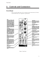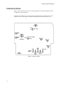
1
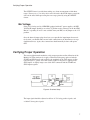
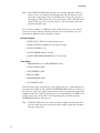
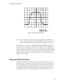
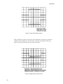
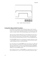
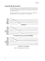
Model 2145
Time to Amplitude
Converter
9231617B
User’s Manual
Copyright 2005, Canberra Industries, Inc. All rights reserved.
The material in this document, including all information, pictures,
graphics and text, is the property of Canberra Industries, Inc. and
is protected by U.S. copyright laws and international copyright
conventions.
Canberra expressly grants the purchaser of this product the right
to copy any material in this document for the purchaser’s own use,
including as part of a submission to regulatory or legal authorities
pursuant to the purchaser’s legitimate business needs.
No material in this document may be copied by any third party, or
used for any commercial purpose, or for any use other than that
granted to the purchaser, without the written permission of
Canberra Industries, Inc.
Canberra Industries, 800 Research Parkway, Meriden, CT 06450
Tel: 203-238-2351 FAX: 203-235-1347 http://www.canberra.com
The information in this document describes the product as
accurately as possible, but is subject to change without notice.
Printed in the United States of America.
Table of Contents
1. Introduction . . . . . . . . . . . . . . . . . . . . . . . . . . . . . 1
2. Controls and Connectors . . . . . . . . . . . . . . . . . . . . . . 3
Front Panel . . . . . . . . . . . . . . . . . . . . . . . . . . . . . . . . . . . . . . . . . . . . . 3
Internal Controls. . . . . . . . . . . . . . . . . . . . . . . . . . . . . . . . . . . . . . . . . . . 4
3. Operation. . . . . . . . . . . . . . . . . . . . . . . . . . . . . . . 5
Installation . . . . . . . . . . . . . . . . . . . . . . . . . . . . . . . . . . . . . . . . . . . . . . 5
Initial Setup . . . . . . . . . . . . . . . . . . . . . . . . . . . . . . . . . . . . . . . . . . . . . 5
Outputs . . . . . . . . . . . . . . . . . . . . . . . . . . . . . . . . . . . . . . . . . . . . . 6
Width . . . . . . . . . . . . . . . . . . . . . . . . . . . . . . . . . . . . . . . . . . . . . . 6
Output Impedance. . . . . . . . . . . . . . . . . . . . . . . . . . . . . . . . . . . . . . . . 6
Valid Conversion . . . . . . . . . . . . . . . . . . . . . . . . . . . . . . . . . . . . . . . . 6
Offset . . . . . . . . . . . . . . . . . . . . . . . . . . . . . . . . . . . . . . . . . . . . . . 6
Bin Voltage . . . . . . . . . . . . . . . . . . . . . . . . . . . . . . . . . . . . . . . . . . . 7
Verifying Proper Operation . . . . . . . . . . . . . . . . . . . . . . . . . . . . . . . . . . . . . 7
Using the SCA Functions . . . . . . . . . . . . . . . . . . . . . . . . . . . . . . . . . . . . . . 9
Using the SCA Functions . . . . . . . . . . . . . . . . . . . . . . . . . . . . . . . . . . . . . 11
Using the Stop Inhibit Function . . . . . . . . . . . . . . . . . . . . . . . . . . . . . . . . . . 12
Using the Coincidence Function . . . . . . . . . . . . . . . . . . . . . . . . . . . . . . . . . . 13
Using the Strobe Function . . . . . . . . . . . . . . . . . . . . . . . . . . . . . . . . . . . . . 14
Operation in a System . . . . . . . . . . . . . . . . . . . . . . . . . . . . . . . . . . . . . . . 15
4. Circuit Description . . . . . . . . . . . . . . . . . . . . . . . . . 16
A. Specifications . . . . . . . . . . . . . . . . . . . . . . . . . . . 19
Inputs . . . . . . . . . . . . . . . . . . . . . . . . . . . . . . . . . . . . . . . . . . . . . . . . 19
Outputs . . . . . . . . . . . . . . . . . . . . . . . . . . . . . . . . . . . . . . . . . . . . . . . 19
Front Panel Controls . . . . . . . . . . . . . . . . . . . . . . . . . . . . . . . . . . . . . . . . 20
Internal Controls . . . . . . . . . . . . . . . . . . . . . . . . . . . . . . . . . . . . . . . . . . 21
Indicators . . . . . . . . . . . . . . . . . . . . . . . . . . . . . . . . . . . . . . . . . . . . . . 21
Performance . . . . . . . . . . . . . . . . . . . . . . . . . . . . . . . . . . . . . . . . . . . . 21
Connectors . . . . . . . . . . . . . . . . . . . . . . . . . . . . . . . . . . . . . . . . . . . . . 22
Power Requirements . . . . . . . . . . . . . . . . . . . . . . . . . . . . . . . . . . . . . . . . 23
Physical . . . . . . . . . . . . . . . . . . . . . . . . . . . . . . . . . . . . . . . . . . . . . . 23
B. Installation Considerations . . . . . . . . . . . . . . . . . . . . 24
ii
1. Introduction
The Model 2145 Time-to-Amplitude Converter/SCA generates a rectangular output
pulse whose peak amplitude is linearly proportional to the time interval between a
START and STOP input pulse pair. The built-in Time Single Channel Analyzer, COINCidence/ANTICOINCidence gating, RESET, STOP INHIBIT features enhance the
Model 2145’s flexibility for your nuclear timing analysis needs.
The basic time-to-amplitude conversion (TAC) analyzes the time relationships between random events, such as nuclear decay, that occur within a selected interval of
time. The Model 2145 is ideal for time of flight, positron lifetime, pulse shape analysis
in particle studies, and pulse pair timing in position sensitive detector systems.
To meet these needs, the Model 2145 offers 15 time ranges from 20 ns to 1 ms, with a
jumper selectable time offset extending the useful range of the two shortest time
ranges. The positive unipolar TAC output is essentially flat topped for accurate measurement by an ADC.
Internal gating prevents a TAC output pulse for overrange START to STOP time differences, STOP inputs received prior to an accepted START, and START or STOP
signals received during the converter busy time. The front panel OVERRANGE,
VALID CONVERSION and BUSY LEDs simplify setup of the instrument. The COINCidence/ANTICOINCidence gating feature permits prompt (early) gating of a
START/STOP pulse pair and is best used to minimize conversion time on unwanted
pulses.
The single channel analyzer (SCA) portion of the Model 2145 operates on the TAC
output pulse amplitude, and places equivalent timing restriction on the time spectrum
being accumulated. For a selected TIME RANGE, a 0 to 100% time window can be
selected with the front panel TIME and ∆ TIME ten-turn locking-dial potentiometers.
An SCA logic output is produced for every TAC pulse whose peak amplitude falls between the TIME setting and the sum of TIME plus ∆ TIME settings. A front panel
SCA IN/OUT switch lets the TAC output be gated by the SCA output, or be generated
normally.
Both the TAC and SCA outputs are simultaneously adjustable in width (internal
jumper plug for 0.5, 1.0, or 2.5 µs) and are synchronous, so timing jitter on the SCA
output is essentially non-existent. The front panel DELAY allows selection of the delay between the receipt of a STOP signal and the generation of an output signal.
Introduction
Following a valid conversion, the STROBE function allows an external control signal
to determine if and when a TAC output is generated. The start and duration set the
time window during which a strobe signal will be accepted. They are controlled by the
DELAY and CONV READY signals respectively. In the EXT STROBE Mode, the
DELAY and CONV READY signals allow minimization of system dead time.
VALID START and VALID STOP outputs represent the time interval from the accepted START or STOP until TAC reset occurs. The front panel STOP INHIBIT adjustment allows rejection of STOP input signals in a range of 1% to 100% of each time
range. This is useful for suppressing unwanted inputs in applications such as linear accelerators, and prevents false outputs. A MONITOR output is provided; when its output is true, STOP pulses are inhibited.
The RESET/INHIBIT input permits late anticoincidence gating. It is used to terminate
a conversion cycle and prevent subsequent conversions while driven. For example, it
can prevent a TAC output based on slow energy analysis.
The VALID START, VALID STOP, SCA, CONV READY, and MONITOR outputs
are each internally selectable as positive voltage pulses or negative fast NIM current
pulses. Each positive output is source matched with a 50 ohm series resistive termination, preventing ringing on unterminated cables, which can cause multiple counting.
2
Front Panel
2. Controls and Connectors
Front Panel
This is a brief description of the 2145’s front panel controls and connectors. For more
detailed information, refer to Appendix A, Specifications.
Figure 1 Front Panel
3
Controls and Connectors
Internal Controls
Figure 2 shows the location of 2145’s internal jumpers. For detailed information, refer
to Appendix A, Specifications.
The jumpers should be set to your specific requirements before applying power to the
module. Access to the jumpers is obtained by removing the unit’s left side cover.
Figure 2 Internal Controls
4
Installation
3. Operation
This section outlines the operation of the Model 2145 TAC/SCA. Following these procedures will make.you familiar enough with the instrument to be able to use it effectively in any situation.
Installation
The Canberra Model 2000 Bin and Power Supply, or equivalent, will accommodate
the Model 2145. The right side cover of the two-width NIM module acts as a guide for
insertion of the instrument. The module is secured in place by turning the two
front-panel captive screws clockwise until finger tight. It is recommended that the
NIM bin power switch be OFF whenever the module is installed or removed.
The Model 2145 can be safely operated where the ambient air temperature is between
0 and 50 °C (120 °F, maximum). Perforations at the top and bottom of the unit permit
cooling air to circulate through the module. When rack mounted along with other heat
generating equipment, adequate clearance should be provided to allow for sufficient
air flow through both the perforated top and bottom covers of the NIM bin.
Initial Setup
If you want to use the internal controls in other than their default settings (Figure 2),
you should remove the left side cover of the instrument and set the internal jumper
plugs to provide the desired input and output characteristics. Canberra recommends
that you make these selections with the 2145's power OFF.
INPUTS: The polarity of the START, STOP, GATE, STROBE and RESET input signals is selected by jumper plugs. Since most fast timing discriminators provide a negative output, these jumpers are shipped in the negative position and should be changed
only if the input signal is positive.
Since reflection-induced ringing can cause timing degradation, both polarities of the
START, STOP and GATE inputs are terminated in 50 ohms.
The input circuits for STROBE and RESET/INHIBIT each accept positive voltage or
negative current NIM pulses without the need for polarity selection switches. The input impedance for the negative current pulse is 50 ohms. The input impedance for the
positive voltage pulse is 1 kilohm. If it is necessary to decrease the impedance at the
STROBE or RESET inputs in order to minimize reflection induced ringing, an external 50 ohm terminator can be connected to the input BNC. Ringing can be caused by
fast rise time signal sources or long cable lengths.
5
Operation
Outputs
The VALID START, VALID STOP, SCA, MONITOR, and VALID CONVERSION
outputs each may be selected individually to provide a positive voltage or a negative
current NIM pulse. The positive voltage pulse output provides a 50 ohm nominal
source impedance to prevent ringing and pulse reflections, which can cause spurious
effects or multiple pulse counting. The negative current pulse output is shunt terminated in 50 ohms nominal for the same reason.
You can select the positive voltage pulse by setting the appropriate jumper near the
identified output to +, and the negative current output by setting the jumper to –.
Width
The TAC output pulse may be set for a nominal width (at the 50% level) of 0.5, 1.0, or
2.5 µs to accommodate the pulse requirements of the ADC being used. In each case,
the rise time of the output pulse is controlled to 0.25 ps to prevent slew-rate induced
errors in the peak detector of the ADC. You should set the WIDTH jumper plug to the
desired pulse width.
Note: The SCA output pulse (either positive or negative) will have the same width as
the TAC output as selected above.
Output Impedance
The output impedance of the TAC output may be selected as either 10 ohms or 93
ohms. Use 10 ohms for driving short lengths of cable connected to an MCA. For long
cable runs or when source matching is desired, use 93 ohms. The TAC is designed to
generate a full scale 10 V output when fed into a high input impedance which is characteristic of many MCA's including Canberra's. To drive ADC's with 50 ohm inputs, it
is recommended that the 2145's output impedance be set at 93 ohms. This will preserve linear operation of the 2145, although the output voltage will be reduced.
Valid Conversion
The width of the Valid Conversion signal which is available at the CONVERSION
READY output is adjustable using a front panel potentiometer. The Valid Conversion
jumper plug selects the adjustment range, either 2 to 20 ps or 20 to 200 µs.
Offset
In order to extend the linearity of the 2145 when extremely short time measurements
are being made, a voltage equivalent to approximately 5 ns is subtracted from each
output pulse when the OFFSET jumper is set to the ON position. This jumper affects
only the 20 ns and 50 ns time scales.
6
Verifying Proper Operation
The OFFSET feature is useful when making very short measurements within those
ranges. If necessary, a 5 ns delay cable can be inserted at the STOP input to cancel the
effect of the offset while preserving the extra range gained by using the OFFSET
feature.
Bin Voltage
If the 2145 is being used in a NIM BIN equipped with ±6 V power supplies, the BIN
VOLTAGE jumper should be set to the 6 V position to take advantage of the the NIM
Bin's 6 V capability. If ±6 V is not available from your BIN, set the jumper to the 12 V
position.
Once the internal jumper plugs have been set to provide the input/output characteristics desired, you should make external cable connections to the instrument to set up a
familiarization test. Again, these connections should normally be done with power
OFF.
Verifying Proper Operation
The most straightforward method to verify proper operation and/or calibration of the
Model 2145 Time Analyzer is to apply a known fixed-frequency pulse to both the
START and STOP inputs and to observe the amplitude of the TAC output. As illustrated in Figure 3, a pulse wave form (either positive or negative) is applied to the
STOP inputs. A slightly longer coax cable and T-connector link the START and
STOP inputs together.
Figure 3 Checkout Setup
The input signal should be adjusted to deliver ≥2 V if using positive signals, and
≥–800 mV for negative signals.
7
Operation
Note: With START and STOP linked together, the net input impedance will be reduced to as low as 25 ohms in this demonstration, and will attenuate a pulse
generator's normal output. Since the START signal is delayed by the extra cable length, the STOP signal arrives first and is ignored. Thus, a START signal
and the STOP signal one cycle later generate a conversion time equal to the
period of the input signal.
For a reference condition, a 1 MHz pulse with a width of up to 0.5 µs, or a suitable
square wave from a laboratory function generator, may be used initially. It is suggested that the Model 2145 be configured as follows:
Internal Jumpers
• START, STOP, GATE as needed for input signal
• LOGIC OUTPUT POLARITY set for negative output
• OUTPUT WIDTH to 1 ps
• OUTPUT IMPEDANCE to 10 ohms
• VALID CONVERSION INTERVAL to 1–20 µs range
Front Panel
• TIME RANGE to 20 ns *MULTIPLIER to X100
• COI NC/ANTI to ANTI
• STOP INHIBIT to OFF
• DELAY to MIN
• STROBE MODE to INT
• SCA ON/OFF to OFF
Given the above setup, you should see a TAC output pulse of 5 V peak amplitude on
an oscilloscope (Figure 4). The VALID CONVERSION LED will be lit. A change in
the frequency (rate) of the applied input will then result in a proportional change in the
amplitude of the TAC output. By reducing the rate to approximately 0.45 MHz (2.2 µs
period), the user may verify that the TAC output disappears and the front panel
OVERRANGE indicator will come on.
Note: The BUSY LED will be green when no input is applied. It will become more
red as the input frequency is increased and the module spends more and more
time processing pulses.
8
Using the SCA Functions
Figure 4 Typical TAC Output Signal
Note: Because of the internal analog and logic propagation delays of the Model
2145, a cable about 10 feet (3 m) in length should be used between the tee connector and the START input to obtain a useful TAC output using this setup.
At this point you can examine the VALID START, VALID STOP, and SCA output
pulses in either + or – modes (see “Using the SCA Functions”, below). In Figure 5, a
2:1, 50 ohm attenuator is connected to one of the oscilloscope inputs. This attenuator
will preserve pulse fidelity which may otherwise be degraded by oscilloscope input capacitance. When using the positive logic outputs of the 2145, the attenuator at the oscilloscope input is not necessary and the input impedance at the oscilloscope input
should be set to 1 megohm.
Using the SCA Functions
The Time Single Channel Analyzer function is most commonly used to restrict the
spectrum of pulse pairs received by the instrument to a narrow range of most interest
in a given experiment. These may represent specific coincidences from several detectors, particle disintegrations, annihilations, lifetimes, etc. The Time SCA function
evaluates the result of a given time-to-amplitude conversion and generates a logic output for input time differences within the bounds set by the front panel controls.
9
Operation
Figure 5 Typical SCA Output Pulses
Figure 5 illustrates positive and negative SCA output pulses using the prescribed terminations. Figure 6 illustrates the aberrations caused by ungrounded oscilloscope
probes (top) and oscilloscope input capacitance (bottom).
Figure 6 Negative SCA Output Pulses
10
Using the SCA Functions
Using the SCA Functions
The Time Single Channel Analyzer function is most commonly used to restrict the
spectrum of pulse pairs received by the instrument to a narrow range of greatest interest in a given experiment. These may represent specific coincidences from several detectors, particle disintegrations, annihilations, lifetimes, etc. The Time SCA function
evaluates the result of a given time-to-amplitude conversion and generates a logic output for input time differences within the bounds set by the front panel controls.
The TIME control on the front panel sets the lower limit for the SCA region or window, as scaled from 0 to 100% of any selected time range. The TIME control sets the
width of the SCA window over the same 0 to 100% range, so that the upper limit of
time is read as the sum of the TIME and ∆TIME dial settings.
The logic output decision of the SCA function may be used to gate the TAC output so
that only those pulses within the set SCA limits will be delivered to an external ADC
for analysis. This is done by setting the front panel SCA ON/SCA OFF switch to SCA
ON. When this switch is set to SCA OFF, all outputs will be delivered to the ADC.
Note: The VALID CONVERSION indicator is not affected by the SCA on/off
switch because that indicator shows only if the inputs are within the TIME
RANGE and MULTIPLIER switch settings.
Using the settings on page 8, but with SCA ON, the front panel TIME control set to
2.0 and the ∆TIME control to 6.0, an oscilloscope observation of the TAC output will
be seen only for pulses between 2.0 and 8.0 V as the input test frequency is varied up
and down.
Figure 7 shows the Model 2145's differential nonlinearity as observed on a Canberra
MCA using random noise pulses to generate a time spectrum on the 20 x100 ns range,
and with the SCA set as above. The sharp skirts of the spectrum attest to the precision
of the SCA built into the Model 2145.
11
Operation
Figure 7 2000 ns Differential Nonlinearity
Using the Stop Inhibit Function
It is possible in some experiments to have STOP pulses that are caused or contaminated by noise or pulse reflections. If these unacceptable STOP pulses are not rejected
in some way, they will initiate unintended time analysis cycles, contribute to the Time
Analyzer's dead time, and thus affect the high throughput qualities of the Model 2145.
Why not use the self-contained Time SCA to reject these STOP pulses? By creating a
time window which would restrict the TAC output to acceptable pulse pairs the noise
pulses could be kept from generating a TAC output. However, this would still incur
increased dead time and possibly block time analysis on a desired START/STOP pair.
The STOP INHIBIT function has been designed to overcome this limitation by setting
a "time threshold" just before an acceptable STOP pulse. The Time Analyzer will not
recognize STOP pulses which are below this threshold.
By careful adjustment of the STOP INHIBIT control, unacceptable (early) STOP input
pulses can be suppressed, reducing excessive Time Analyzer dead time and the generation of false TAC outputs. As an aid in setting the Inhibit threshold, the MONITOR
output BNC provides a logic pulse whose width is equal to the blocking time interval
following an accepted START input pulse.
Figure 8 illustrates the effect of a STOP INHIBIT set at approximately 10% of the 1 µs
range of the Model 2145, as seen on a flat time spectrum using random pulser inputs.
12
Using the Coincidence Function
Figure 8 Effect of a Stop Inhibit on a Time Spectrum
Using the Coincidence Function
The most common use of the Coincidence function is for early (prompt) gating of
START/STOP pulse pairs as an aid in reduction of the Time Analyzer's dead time.
Since the internal logic of the Analyzer is set to reject any STOP pulses that arrive before an accepted START pulse, a means of accepting or rejecting a START pulse will
allow the operator to control pulse pair conversion.
By selecting one of the two modes of gating and applying a specified signal to the
GATE connector, the operator can enable or disable the acceptance of a START pulse,
and thus the conversion of any pulse pairs.
In the COINCidence mode, an applied GATE signal will enable the operator to select
a START pulse for beginning a conversion cycle. Only START pulses coincident with
the GATE pulse are allowed to initiate a conversion. Pulse pairs that are not coincident
will not be processed by the Analyzer.
In the ANTICOINCidence mode, conversions will be inhibited for START pulses coincident with the GATE signal. All other pulse pairs will be converted.
In either mode, an applied GATE signal will affect acceptance of a START pulse if
the GATE signal is received at least 10 ns prior to the START pulse and overlaps the
START pulse by approximately 50 ns.
Note: If the Coincidence function is not to be used, the mode switch must be left in
the ANTICOINCidence position and the GATE input must be left open.
13
Operation
Using the Strobe Function
The Strobe function allows external logic to determine whether and when a TAC output is generated. This occurs after the TAC conversion and reduces ADC dead time by
preventing undesired TAC outputs. Figure 9 shows timing diagrams, illustrating the
use of the Strobe function.
When the Strobe Mode switch is set to INTernal, the TAC functions normally. After
the DELAY period, every conversion produces a TAC output pulse.
Figure 9 Timing Relationships of TAC Signals
14
Operation in a System
In the EXTernal Strobe Mode, an external Strobe signal must be applied during the
VALID CONVERSION interval to produce a TAC output pulse. This interval starts at
the end of DELAY and has a width determined by the front panel CONV READY
WIDTH potentiometer and the internal VALID CONVERSION INTERVAL jumper.
If a Strobe signal is applied during the VALID CONVERSION interval, a TAC output
pulse will be generated immediately. If the Strobe signal is absent during the VALID
CONVERSION interval, the TAC is reset at the end of VALID conversion and no output pulse is generated.
Operation in a System
The 2145 can be operated with either synchronous or random inputs. When synchronous inputs are present, start/stop time intervals may all be within the VALID
CONVERSION time range shown by the front panel indicator. With random inputs
however, such as those generated by a radioactive source, the start/stop time intervals
may be random in which case both the VALID CONVERSION and OVER RANGE
indicators will be lit.
In some cases it may be advantageous to exchange the START and STOP inputs. This
is often done if the start (excitation) rate is much higher than the stop (response) rate.
To minimize the dead time of the 2145 in this situation the input representing the response can be connected to the START input and the input representing the excitation
can be delayed and connected to the STOP input. The delay is picked to equal the time
range of interest as set on the front panel.
The spectrum obtained from this setup will be inverted, with events representing short
excitation/response time intervals appearing at the high end of the spectrum, since the
time measured by the 2145 is now the excitation/response interval subtracted from the
delay time. Dead time, which can be monitored with the BUSY indicator, is now minimized, since the STOP input circuit will ignore stop inputs received during processing
time.
15
Circuit Description
4. Circuit Description
The Model 2145 Time to Amplitude Converter (TAC) is shown in block diagram form
in Figure 10. The basic time to amplitude converter consists of an integrator which operates by charging a capacitor with a constant current during the time interval from a
START signal to a STOP signal. The current linearly charges the capacitor, producing
a ramp voltage. The charging process stops when the STOP signal is received. The
voltage present on the capacitor is linearly proportional to the START to STOP time
interval.
Figure 10 Model 2145 Block Diagram
The other portions of the circuitry shown in the block diagram serve to interface the
time to amplitude integrator circuit to the inputs and outputs of the TAC or to provide
various other logic or control functions. The input circuits and the latches generate signals which control the switches associated with the integrating capacitor and the current source. The capacitor buffer is a high input impedance, low output impedance
circuit which provides drive capability to the output linear gate and amplifier as well
as the various comparators for the OVERRANGE, SCA, and MONITOR functions.
The control logic generates control signals which activate various portions of the
circuit sequentially during each conversion.
16
Input signals are applied to the START, STOP, and GATE input circuits. All three circuits are substantially the same. Each consists of a high speed comparator with the capability of responding to a positive or negative NIM input signal with the polarity
chosen by the position of the input jumper. When a suitable input occurs, the comparator output changes state and provides a logic signal to drive the inputs of, the latches
that follow. The input, circuits are very fast and are limited in count rate primarily by
the width of the input signal. This allows high count rate signals to be applied directly
to the TAC input, with no timing degradation.
The START and STOP input circuits drive the clock inputs of high speed ECL D-type
latches. The GATE input circuit drives the D input of the START latch and is able to
provide fast COINCIDENCE/ANTICOINCIDENCE gating. The second START latch
output drives the D input of the second STOP latch. and ensures that STOP signals
prior to a START signal are signal rejected. The STOP INHIBIT signal drives the D
input of the first stop latch to prevent unwanted stop commands from being recognized. After level shifting, the outputs from the START and STOP latches are used to
directly control the current source which charges the integrating capacitor and the FET
which resets the ramp voltage to zero.
In order to provide the 2145's various RANGE and MULTIPLIER settings, both the
current source and the integrating capacitor are variable. The current source, consisting of the operational amplifier A2 and transistor Q2B is varied with the front panel
RANGE switch to provide the 20, 50, and 100 RANGE settings. Likewise the integration capacitor, consisting primarily of C23, C12, C13 or C14, is chosen with the front
panel MULTIPLIER switch.
Prior to a conversion, the integrating capacitor is clamped at a quiescent voltage level
determined by the current through source Q15C and the on resistance of clamp FET
Q6C. At the start of the conversion, the clamp transistor (Q18) is turned off by a logic
signal from the START latch, thus steering the source current to the integrating capacitor. This results in a positive going ramp,n on the integrating capacitor. When a STOP
signal is received, the current from source Q2B is steered away from the integrating
capacitor by Q15B which turns on as Q15C turns off. The integrating capacitor retains
the charge it received during the conversion. The charge deposited on the integrating
capacitor is the product of the. charging current and the start/stop time interval, resulting in a fixed voltage which represents the time interval converted.
Transistors Q25, Q26 and Q27 form a buffer which provides a high impedance load on
the integrating capacitor. This avoids discharging. the \integrating, capacitor while
providing drive capabilities to the output. circuitry and comparators which.follow the
buffer.
17
Circuit Description
Transconductance amplifier A6 and associated circuitry monitor the output of buffer
Q5 and set it to zero volts after the integrating cap is reset. This circuitry compensates
for the quiescent voltage developed across clamp FET Q6C and the offset of emitter
follower Q5. C37 is used as a memory element to store the voltage level necessary to
cancel the offsets. In order to keep the dc level on C37 from being affected by the
ramp signal, amplifier A6 switches off during the start/stop interval. When the
OFFSET jumper is in the ON position, an offset voltage equivalent to approximately 5
ns is subtracted from the buffer output.
Transistors Q3A, Q3B, Q3C and Q3D form a gate which opens to read out the final
ramp level just after the start/stop interval has ended. The gate feeds A4, which together with Q9 and Q10 form the output amplifier whose gain is two. Thus a full scale
conversion generates 5 V on the integrating capacitor and 10 V at the output. The duration of the output pulse is determined by the length of time the gate is opened.
A conversion is considered valid if a STOP signal is received during the conversion
interval. A valid STOP signal initiates tha output sequence controlled by the string of
logic one-shots A13A, A13B, A12B and A16A for DELAY, VALID CONVERSION,
OUTPUT, and RESET, respectively.
After a valid conversion, an output signal is generated by the OUTPUT one-shot and
the entire circuit is RESET. This clears the logic, clamps the integrating capacitor, and
prepares the circuit for the next conversion. If no STROBE signal appears during the
VALID CONVERSION interval or if an OVERRANGE is detected, the circuit is
RESET without generating an output.
Several comparators monitor the output of the buffer: the OVERRANGE comparator,
the two SCA comparators, and the STOP INHIBIT comparator. The OVERRANGE
comparator,detects an overrange condition if the ramp exceeds 5 V. If this occurs, the
converter circuitry is reset without generating an output. The two SCA comparators
determine if the conversion is within the range set by the Lower Level and Upper
Level controls. The STOP INHIBIT comparator determines when a selected percentage of the conversion range has been exceeded and allows STOP inputs to be accepted
after this point if this function is enabled.
A lower limit time cutoff determined by RV8 and C164 is set to reject start/stop intervals less than approximately 5 ns. Since these short intervals are still within the time
range setting the LED indicators are not affected.
Five logic outputs are provided by the 2145: the VALID START, VALID STOP,
SCA, CONVERSION READY, and STOP INHIBIT MONITOR outputs. All are identical and consist of a positive NIM voltage driver and a negative NIM current driver.
The desired output polarity is selected by a jumper plug.
18
Inputs
A. Specifications
Inputs
START – Accepts negative or positive logic signals or levels, internally selected;
shipped in negative position. Negative thresh old –250 mV; positive threshold 1 V;
width ≥2 ns. Zin ≈ 50 Ω, selectable to ≈ 1 kΩ by removal of internal resistor; dc coupled input protected to ±10 V. Leading edge initiates time conversion.
STOP – Input specifications identical to START input. Leading edge terminates time
conversion.
GATE – Input specifications identical to START input. Gates TAC output in either
COINCidence or ANTICOINCidence mode. GATE must begin 10 ns prior to and
overlap START input.
STROBE – Input voltage requirements identical to START input; width ≥50 ns;
Zin ≈ 1 kΩ for positive signals, 50 Ω for negative signals, dc coupled; initiates output
pulse when in EXT strobe mode; must occur in time window set by CONV READY.
RESET/INHIB – Input specifications identical to strobe input; serves as a late anticoincidence input and terminates conversion cycle. The reset period ends at the conclusion of RESET/INHIB or the internal clear time, whichever occurs last.
Outputs
TAC – Provides positive flat topped rectangular unipolar pulse; constant pulse shape
independent of TIME RANGE or amplitude; amplitude proportional to accepted
START/STOP input pulse time difference; adjustable delay (0.5 to 10.5 µs) and width
(0.5, 1.0 or 2.5 µs); rise time ≈ 250 ns; dc coupled; front panel BNC connector.
Zout ≈ 10 Ω or 93 Ω, internally selectable. Shipped set for 10 Ω and 1 ms width; 10 V
full scale into high impedance load.
VALID START (converter busy time) – Provides either TTL compatible positive voltage pulse with Trise and Tfall <25 ns, or –16 mA current pulse with T rise <10 ns; shipped
in negative position; Zout ≈ 50 Ω, dc coupled; duration equal to time interval between
accepted START input and end of cycle reset time.
VALID STOP – Output pulse specifications identical to VALID START; duration
equal to time interval between accepted STOP input signal and end of cycle reset time.
19
Specifications
SCA – Output pulse specifications identical to VALID START; leading edge is in
time coincidence with, and duration is equal to, TAC output.
STOP INHIBIT MONITOR – Output pulse specifications identical to VALID
START; monitors STOP INHIBIT RANGE adjustment.
CONVersion READY – Output pulse specification identical to VALID START. Active from end of DELAY period. Duration set by CONV READY WIDTH control.
Range set by internal jumper, 1 to 20 µs or 10 to 200 µs; shipped in 1–20 µs position.
Indicates period when STROBE input will initiate output pulse.
Front Panel Controls
TIME RANGE – Three-position rotary switch selects full scale time interval of 20, 50,
or 100 ns between accepted START and STOP input pulses.
MULTIPLIER – Five-position rotary switch extends TIME RANGE by X1, X10,
X100, X1K or X10K.
DELAY – 22-turn screwdriver potentiometer varies TAC output delay time; 0.5 to
10.5 µs range, with adjacent toggle switch in VARiable; fixed 150 ns relative to STOP
input with switch in MINimum. Test point monitors the DELAY time setting.
GATE MODE – Toggle switch selects COINCidence or ANTICOINCidence gating.
Time conversion is enabled (COINC) or inhibited (ANTICOINC) upon receipt of a
GATE input signal.
TIME – 10-turn locking dial potentiometer selects minimum time of interest from 0 to
100% of selected TIME RANGE.
∆ TIME – 10-turn locking dial potentiometer selects time window width from 0 to
100% of selected TIME RANGE.
SCA IN/OUT – Toggle switch selects whether TAC output is gated with Time SCA.
STROBE MODE – Toggle switch selects INTernal or EXTernal strobe operation.
CONVersion READY WIDTH – 22-turn, screwdriver adjustable po tentiometer determines time duration during which STROBE input will initiate output pulse; jumper
selectable for 1 to 20 µs or 10 to 200 µs, shipped set for 1 to 20 µs.
STOP INHIBIT – Toggle switch enables (ON) or disables (OFF) STOP INHIBIT
RANGE adjustment.
20
Internal Controls
STOP INHIBIT RANGE – 22-turn potentiometer to reject unwanted STOP input signals from 1% (minimum 20 ns) to 100% of selected TIME RANGE.
Internal Controls
TAC OUTPUT WIDTH – Jumper selects 0.5, 1.0 or 2.5 µs output pulse width for both
SCA and TAC outputs.
TAC OUTPUT IMPEDANCE – Jumper selects Zout = 10 Ω or 93 Ω.
START +/–, STOP +/–, GATE +/–, STROBE +/– RESET +/–: Jumpers determine input polarity of respective signals.
VALID START +/–, VALID STOP +/–, SCA +/–, STOP INHIBIT +/–,
CONVERSION READY +/–: Jumpers select either positive voltage or negative current mode outputs for the respective signals.
CONV READY – Jumper selects 1 to 20 µs or 10 to 200 µs range.
OFFSET ON/OFF – Jumper enables (ON) or disables (OFF) output time offset, extending usable range by ≈ 5 ns when TIME RANGE is set to 20 ns or 50 ns. Shipped
in ON position.
BIN VOLTAGE – Jumper configures 2145 for Bins with 6 V power supply.
Indicators
OVERRANGE – Glows red when START/STOP time interval exceeds selected range.
VALID CONVERSION – Red LED lights when START/STOP time interval and
gating produce a TAC output. Not affected by SCA setting.
BUSY – Bicolor LED is green when TAC is inactive, turns red to indicate significant
count rate.
Performance
TIME RESOLUTION – <0.01% of full scale plus 5 ps FWHM.
21
Specifications
TAC DIFFERENTIAL NONLINEARITY – With OFFSET jumper set to ON, typically ≤±1% (maximum 2%) from lower limit of useable range to full scale. For 20 ns
TIME RANGE, lower limit is 5 ns; for all other TIME RANGEs, lower limit is 10 ns
or 1% of full scale, whichever is greater.
TAC INTEGRAL NONLINEARITY – With OFFSET jumper set to ON, <±0.1% over
useable range, as described in Differential Nonlinearity specification.
SCA TIME/∆ TIME INTEGRAL NONLINEARITY – <±0.5% of full scale.
TAC OUTPUT TEMPERATURE STABILITY – >±0.01%/°C (±100 ppm/°C) of full
scale, plus 10 ps/°C.
SCA TIME/∆ TIME TEMPERATURE STABILITY –>±0.01%/°C (±100 ppm/°C) of
full scale.
OUTPUT DELAY/OUTPUT WIDTH TEMPERATURE STABILITY – >±0.01%/°C
(±100 ppm/°C) of full scale.
TEMPERATURE OPERATING RANGE – 0 to 50 °C.
TAC OUTPUT DROOP – <0.015%/µs of delay from completed conversion to TAC
output. Delay time is determined by front panel DELAY setting or external strobe acceptance, or both.
CONVERTER RESET – 1µs for X1 and X10 multipliers, 5 µs for X100, 40 µs for
X1K and X10K; occurs after TAC output, reset or overrange.
GATE PEDESTAL – Essentially zero pedestal, factory calibrated.
SCA OUTPUT TIME WALK – None, with respect to TAC output.
MINIMUM START TO STOP CONVERSION TIME – ≈ 2 ns.
COUNT RATE CAPABILITY – START, STOP, GATE inputs capable of count rates
greater than 25.
Connectors
All signal connectors are front panel BNCs.
22
Power Requirements
Power Requirements
+24 V dc – 70 mA
+12 V dc – 230 mA
–24 V dc – 30 mA
–12 V dc – 290 mA
Physical
SIZE – Standard double-width NIM module 6.85 x 22.12 cm (2.70 x 8.71 in.) per
DOE/ER-0457T.
NET WEIGHT – 1.3 kg (2.8 lb).
SHIPPING WEIGHT – 2.3 kg (5.0 lb).
23
Installation Considerations
B. Installation Considerations
This unit complies with all applicable European Union requirements.
Compliance testing was performed with application configurations commonly used for
this module; i.e. a CE compliant NIM Bin and Power Supply with additional CE compliant application-specific NIM were racked in a floor cabinet to support the module
under test.
During the design and assembly of the module, reasonable precautions were taken by
the manufacturer to minimize the effects of RFI and EMC on the system. However,
care should be taken to maintain full compliance. These considerations include:
• A rack or tabletop enclosure fully closed on all sides with rear door access
• Single point external cable access
• Blank panels to cover open front panel Bin area
• Compliant grounding and safety precautions for any internal power distribution
• The use of CE compliant accessories such as fans, UPS, etc.
Any repairs or maintenance should be performed by a qualified Canberra service
representative. Failure to use exact replacement components, or failure to reassemble
the unit as delivered, may affect the unit’s compliance with the specified EU
requirements.
24
Canberra (we, us, our) warrants to the customer (you, your) that for a period of ninety (90) days from the date of
shipment, software provided by us in connection with equipment manufactured by us shall operate in accordance
with applicable specifications when used with equipment manufactured by us and that the media on which the
software is provided shall be free from defects. We also warrant that (A) equipment manufactured by us shall be
free from defects in materials and workmanship for a period of one (1) year from the date of shipment of such
equipment, and (B) services performed by us in connection with such equipment, such as site supervision and
installation services relating to the equipment, shall be free from defects for a period of one (1) year from the date of
performance of such services.
If defects in materials or workmanship are discovered within the applicable warranty period as set forth above, we
shall, at our option and cost, (A) in the case of defective software or equipment, either repair or replace the
software or equipment, or (B) in the case of defective services, reperform such services.
LIMITATIONS
EXCEPT AS SET FORTH HEREIN, NO OTHER WARRANTIES OR REMEDIES, WHETHER STATUTORY,
WRITTEN, ORAL, EXPRESSED, IMPLIED (INCLUDING WITHOUT LIMITATION, THE WARRANTIES OF
MERCHANTABILITY OR FITNESS FOR A PARTICULAR PURPOSE) OR OTHERWISE, SHALL APPLY. IN NO
EVENT SHALL CANBERRA HAVE ANY LIABILITY FOR ANY SPECIAL, EXEMPLARY, PUNITIVE, INDIRECT
OR CONSEQUENTIAL LOSSES OR DAMAGES OF ANY NATURE WHATSOEVER, WHETHER AS A RESULT
OF BREACH OF CONTRACT, TORT LIABILITY (INCLUDING NEGLIGENCE), STRICT LIABILITY OR
OTHERWISE. REPAIR OR REPLACEMENT OF THE SOFTWARE OR EQUIPMENT DURING THE
APPLICABLE WARRANTY PERIOD AT CANBERRA'S COST, OR, IN THE CASE OF DEFECTIVE SERVICES,
REPERFORMANCE AT CANBERRA'S COST, IS YOUR SOLE AND EXCLUSIVE REMEDY UNDER THIS
WARRANTY.
EXCLUSIONS
Our warranty does not cover damage to equipment which has been altered or modified without our written
permission or damage which has been caused by abuse, misuse, accident, neglect or unusual physical or
electrical stress, as determined by our Service Personnel.
We are under no obligation to provide warranty service if adjustment or repair is required because of damage
caused by other than ordinary use or if the equipment is serviced or repaired, or if an attempt is made to service or
repair the equipment, by other than our Service Personnel without our prior approval.
Our warranty does not cover detector damage due to neutrons or heavy charged particles. Failure of beryllium,
carbon composite, or polymer windows, or of windowless detectors caused by physical or chemical damage from
the environment is not covered by warranty.
We are not responsible for damage sustained in transit. You should examine shipments upon receipt for evidence
of damage caused in transit. If damage is found, notify us and the carrier immediately. Keep all packages,
materials and documents, including the freight bill, invoice and packing list.
When purchasing our software, you have purchased a license to use the software, not the software itself. Because
title to the software remains with us, you may not sell, distribute or otherwise transfer the software. This license
allows you to use the software on only one computer at a time. You must get our written permission for any
exception to this limited license.
BACKUP COPIES
Our software is protected by United States Copyright Law and by International Copyright Treaties. You have our
express permission to make one archival copy of the software for backup protection. You may not copy our
software or any part of it for any other purpose.
Revised 1 Apr 03