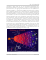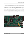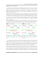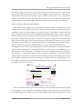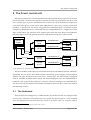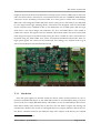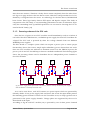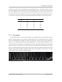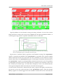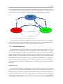
1
MASTER THESIS v47 Design and implementation of a highreliability DCS-Board power control system for the ALICE TRD detector Dipl. Ing (FH) Jens Steckert Contents 1 Abstract....................................................................................................................... 6 2 LHC, ALICE and the TRD.......................................................................................7 2.1 The Large Hadron Collider (LHC)......................................................................................7 2.2 ALICE......................................................................................................................................10 2.2.1 The quark gluon plasma (QGP)..................................................................................10 2.2.2 Quark gluon plasma and the formation of the universe........................................ 10 2.2.3 The ALICE detector......................................................................................................12 2.2.4 The transition radiation detector (TRD)....................................................................13 2.3 DCS board..............................................................................................................................16 2.4 DCS Power supply in general............................................................................................17 3 Reliability and redundancy.................................................................................. 18 3.1 Overall View..........................................................................................................................18 3.1.1 Coupling of the redundant signals.............................................................................19 3.2 Subsystems.............................................................................................................................20 3.2.1 The power control unit (PCU).....................................................................................20 3.2.2 The power distribution control board (PDC)...........................................................20 3.2.3 The power distribution box (PDB).............................................................................20 3.2.4 Transmission line..........................................................................................................21 3.3 Considerations concerning redundancy..........................................................................21 3.3.1 Benefits of the parallel structure ................................................................................22 3.3.2 Critical elements............................................................................................................23 3.4 Normal state of operation...................................................................................................24 3.5 Reliability measurements...................................................................................................25 3.6 Conclusion.............................................................................................................................25 4 The power distribution control board................................................................ 26 4.1 Conception.............................................................................................................................26 4.1.1 Radiation tolerance.......................................................................................................26 4.1.2 Tolerance to magnetic fields........................................................................................27 4.1.3 Ground free data transmission ..................................................................................28 4.1.4 Compatibility with existent power distribution box...............................................28 4.1.5 Data transmission medium.........................................................................................28 4.1.6 Data encoding................................................................................................................29 Master Thesis, Jens Steckert Page 2 of 112 4.2 Requirements for the logic device....................................................................................29 4.3 The Actel 54SX08A FPGA...................................................................................................31 4.4 General Architecture............................................................................................................33 4.4.1 Optional Circuitry.........................................................................................................34 4.4.2 Configuration.................................................................................................................34 4.4.3 Service sub circuits........................................................................................................35 4.5 FPGA Design.........................................................................................................................36 4.5.1 The top entity.................................................................................................................36 4.5.2 Status generation entity (statled2)..............................................................................37 4.5.3 Serial to parallel shift register (shreg)........................................................................38 4.5.4 Serial to parallel shift register with parallel load (shreg_p)...................................38 4.5.5 The toggle register (treg)..............................................................................................38 4.5.6 The hamming encoder / decoder (hm_enc_dmem/hm_dec_dmem)....................39 4.5.7 The transmission line supervisor module.................................................................39 4.6 Device utilization.................................................................................................................41 4.7 Data transmission.................................................................................................................41 4.7.1 Dimensioning the optocoupler circuit.......................................................................43 4.7.2 Timing and sampling points of the PDC feedback signal......................................45 4.7.3 The serial protocol.........................................................................................................48 4.7.4 Data path in the Actel FPGA of the PDC..................................................................50 4.7.5 Faulty cable diagnosis..................................................................................................51 4.8 Detailed measurements on the PDC.................................................................................52 4.8.1 Measurement of signal deformations .......................................................................52 4.8.2 Conclusion......................................................................................................................55 5 The Power control unit.......................................................................................... 56 5.1 The Hostboard.......................................................................................................................56 5.1.1 Line driver......................................................................................................................57 5.1.2 Powering scheme of the PCU rack.............................................................................58 5.1.3 Front panel.....................................................................................................................59 5.2 The DCS board......................................................................................................................60 5.2.1 The ALTERA Excalibur device ..................................................................................60 5.2.2 The Avalon interface ....................................................................................................60 5.3 General FPGA design..........................................................................................................63 5.3.1 PCU data flow ...............................................................................................................64 Master Thesis, Jens Steckert Page 3 of 112 5.3.2 The central state machine.............................................................................................65 5.3.3 Feedback input logic.....................................................................................................67 5.3.4 Clock domain crossing.................................................................................................68 5.3.5 Transmission data flow................................................................................................70 5.3.6 The status entity............................................................................................................71 5.3.7 Indication lights.............................................................................................................71 5.3.8 The timeout mechanism...............................................................................................72 5.3.9 FPGA Utilization...........................................................................................................73 5.3.10 Data words...................................................................................................................73 6 The power distribution box ................................................................................. 76 6.1 Overview................................................................................................................................76 6.2 Working principle and measurements.............................................................................77 6.2.1 Original state..................................................................................................................78 6.2.2 Modifications of the switching behavior...................................................................79 6.2.3 Unexpected side effect of the FET change.................................................................80 6.2.4 The FET replacement....................................................................................................81 6.2.5 Operation of the modified PDB with the new FET..................................................82 6.2.6 Variation of the buffer capacity..................................................................................83 6.2.7 Variation of R1...............................................................................................................83 6.2.8 Analysis of the circuit behavior..................................................................................84 6.2.9 Summary of the PDB channel circuit modifications............................................... 87 6.2.10 Possible solutions........................................................................................................87 6.3 Load behavior of the power distribution box.................................................................89 6.3.1 Setup................................................................................................................................89 6.3.2 Measurement of a current pulse.................................................................................90 6.3.3 Measuring the behavior of the power supply with regulation............................. 91 6.3.4 Switching process of the PDB using blocks of four channels................................ 92 6.3.5 Ramp up of all channels, single channel only..........................................................92 6.4 Conclusion.............................................................................................................................93 7 Software....................................................................................................................94 7.1 Overview ...............................................................................................................................94 7.1.1 Local software................................................................................................................95 7.2 SCOMM3 LINUX device driver........................................................................................95 7.3 The static library libsw........................................................................................................98 Master Thesis, Jens Steckert Page 4 of 112 7.4 DIM Server...........................................................................................................................100 7.4.1 Modified DIM Server..................................................................................................101 8 Conclusion............................................................................................................. 103 9 Appendix................................................................................................................ 104 9.1.1 corrupt data line table................................................................................................104 9.2 The PCU DIM server command guide v.02 ..................................................................104 9.2.1 Command format........................................................................................................104 9.2.2 Commands...................................................................................................................105 9.3 Libsw translation table......................................................................................................106 9.3.1 Cables and connectors................................................................................................107 Master Thesis, Jens Steckert Page 5 of 112 Abstract 1 Abstract The ALICE detector at the Large Hadron Collider (LHC) at CERN will be used to observe a new state of matter, the quark gluon plasma. Consisting of several sub detectors including the ITS, TPC and TRD detector this particle detector is able to detect particles at high multiplicities. The transition radiation detector (TRD) is used to extend the particle tracking range of the TPC and differentiates between electrons and pions. The read-out electronics of the TRD is controlled by the Detector Control System (DCS) board. This compact board hosting an embedded LINUX system is based on the ALTERA Excalibur device, a FPGA with embedded ARM processor core. Due to the critical role of the DCS board in the TRD, it is powered separately from the front end electronics. Each of the eighteen TRD super-modules is equipped with a power distribution box which distributes the common DCS power to the modules' thirty DCS boards. The PDB enables independently switchable power for each DCS board. The control of the power distribution box was realized by two power distribution control boards (PDC) which are located inside the PDB. Due to the high requirements in reliability the PDC is based on an Actel anti fuse FPGA which provides outstanding radiation hardness and is independent from external memory. The PDC units of the TRD are controlled by four PCU units which are based on the DCS board. Since these devices are located outside the magnet, the requirements in radiation hardness and reliability are lower. Hosting a DIM server, these devices are the link between the low level PDC units and the high level detector control system. The data transmission between PDC and PCU is implemented as a proprietary optocoupler based serial data transmission line which operates at low speed. Using an error tolerant data encoding scheme as well as two independent data transmission systems per PDB the transmission is considered to be highly reliable. The DCS power supply control system had been excessively tested during the construction and testing phase of the first ALICE TRD module in Heidelberg. Further tests had been done after shipping in CERN. Several modification on the existing power distribution box as well as on software improved stability and reliability of this system. Master Thesis, Jens Steckert Page 6 of 112 LHC, ALICE and the TRD 2 LHC, ALICE and the TRD This chapter will show the context in which the project of designing a power supply control system is embedded. Starting from the general description of the LHC the focus points on the ALICE detector and here the TRD is of special interest. Since ALICE is designed to observe the quark gluon plasma, a short introduction is given to this new state of matter. 2.1 The Large Hadron Collider (LHC) The Large Hadron Collider is a next generation particle accelerator currently built at the European Organization for Nuclear Research (CERN) in Geneva, Switzerland. The LHC is supposed to be ready for operation end of 2007. It is located in the tunnel of the former Large Positron Collider (LEP). The accelerator is located north of the CERN main area. Its circular tunnel with a circumference of 27km spans between the French Jura mountains and the Geneva lake. While the LEP was designed to accelerate leptons (electrons and positrons) the LHC is built for two different operation modes. Proton-Proton collisions will take place at energies of 14TeV while collisions of lead ions will have an accumulated energy up to 1150 TeV. Existing CERN infrastructure including the Proton Synchrotron (PS) and the Super Proton Synchrotron (SPS) is used for generation and injection of the beam into the LHC. Two beams of opposite direction are accelerated until their final energy is reached. Four interaction points are located at different sites around the LHC. The experiments are located at these interaction points where the collision between the accelerated beams takes place. Four main experiments are in construction: ● ATLAS (A Toroidal LHC Apparatus) ● CMS (Compact Muon Solenoid) ● LHCb (LHC Beauty Experiment) ● ALICE (A Large Ion Collider Experiment) ATLAS and CMS are designed to observe proton-proton interactions. They are intended to analyze the nature off matter. The detection of the Higgs Boson is the intended main goal of the ATLAS detector. Verification of theoretical models beyond the standard model is another important task for those detectors. Especially LHCb is built to observe CP violations in b meson systems. The results are used to understand the imbalance in symmetry between matter and antimatter. While three experiments mainly profit from p-p collisions the fourth experiment, the ALICE detector was constructed to observe collisions between Master Thesis, Jens Steckert Page 7 of 112 LHC, ALICE and the TRD relativistic heavy ions. In Pb mode the LHC will accelerate lead ions to collision energies up to 1150 TeV. The observation of the Quark-Gluon plasma which is believed to formate at such energies is the main focus of this detector. With LHC a new generation particle accelerator will be put into operation. The collision energies for heavy ions will be up to 30 times larger than those of the Relativistic Heavy Ion Collider (RHIC) at Brookhaven National Laboratory (BNL). Luminosity, a measure for the rate of events in a specific process, will be more than two times larger. In proton-proton mode the luminosity of LHC will exceed existing accelerators by two orders of magnitude. Collision energies will be up to seven times larger than the highest energies achieved with the Tevatron at Fermilab. As a conclusion it can be stated that LHC will be the most advanced particle accelerator for the next two decades.[1] The following pictures shows the location of the LHC in vicinity of Geneva. A scheme of the different accelerators at CERN is shown in Fig 2 Fig 1: Picture of LHC, CERN and vicinity [1] Master Thesis, Jens Steckert Page 8 of 112 LHC, ALICE and the TRD Fig 2: Accelerator system of CERN Master Thesis, Jens Steckert Page 9 of 112 LHC, ALICE and the TRD 2.2 ALICE It is expected that in collisions of heavy ions at energies achieved with the LHC a new state of matter formates, the quark gluon plasma. The Alice detector was built to investigate this new state of matter. The following subsections will have a look on the ALICE detector and especially the ALICE TRD. 2.2.1 The quark gluon plasma (QGP) In traditional physics a plasma is a state of matter where the gaseous atoms are partly or fully decomposed to electrons and ions. This decomposition is caused by heat and/or high pressures. In a plasma the particles can move freely, is can be compared with a sea of free building blocks of the former particles. In case of the electromagnetic plasma, the electrons and ions move independently. Electrons and ions are charged but from a macroscopic point of view the system is neutral in respect of charge. Since electrons and ions are the constituent of atoms the same is valid for quarks and gluons as basic elements for protons and neutrons. At temperatures about 100.000 times higher than in the middle of the sun the energy is high enough to break the strong bounds between quarks. The formation of a plasma of free quarks and gluons (their interaction particles) starts. While the “traditional plasma” overcomes the electromagnetic force the quark gluon plasma sets the particles free from the strong interaction. Like a traditional plasma the QGP is neutral in terms of charge, color charge and flavor. Fig 3 shows a phase diagram of matter Fig 3: QGP phase diagram (adapted from [2]) 2.2.2 Quark gluon plasma and the formation of the universe The universe passed this state of matter about 1μs after the Big Bang. The standard theory states that in the beginning of the universe all particles, antiparticles and interaction particles had been in thermodynamic equilibrium. After 10-35 s after the big bang, the strong force decoupled from the electro-weak force. After this phase almost all quarks could only convert to quarks an leptons only to leptons. Another 10-11 seconds later the universe had Master Thesis, Jens Steckert Page 10 of 112 LHC, ALICE and the TRD cooled down to 100GeV. At this time weak force decoupled from electromagnetic force. During that time, all matter of the universe was in the state of a Quark Gluon plasma. The QGP existed until 10-6 s the big bang. After that time the universe was cooled down to a temperature of 100MeV. At this temperature the quarks and gluons started to combine to hadrons, the QGP era ended. At a time of 0.01 ms after big bang, all quarks and gluons had been condensed to hadrons like protons and neutrons. Almost all antimatter has been annihilated leaving behind only a few anti-particles. The universe still expanded rapidly and hence cooled down. At a time of 3 minutes the formation of the first light elements, mainly hydrogen, helium and a small amount of lithium stated. During that time most of the electrons remained freely moving between the ionized elements, hence the universe reached the state of a “conventional” plasma. From that time on, the processes had been slowed down dramatically and it took about 380,000 years to reach a state where the plasma had cooled down to an extend where most of the electrons are trapped in atoms. At that time the universe became transparent for photons. Another 200 million years later the temperature had cooled down to 4000 kelvin, gravity had clustered the matter to first stars which from that time on generated all the other heavy elements. In the time until now the universe generated all planets, stars and galaxies known. Since the big bang the universe is expanding. First at a rapid speed, later the expansion was slower. Unlike former theories the universe seems to accelerates again its pace of expansion. [1][3] QGP Fig 4: History of the Universe [3] Master Thesis, Jens Steckert Page 11 of 112 LHC, ALICE and the TRD 2.2.3 The ALICE detector At the collision point of two heavy ions at very high energies a QGP will formate. As higher the energies as longer the QGP persists. Since the QGP cannot be detected directly, the particles which formate from the plasma are observed. The ALICE detector will be capable to observe up to 20,000 particles simultaneously. From the knowledge about the particles generated by the plasma, the reactions taking place within the plasma can be reconstructed. The ALICE detector consists of over 15 sub detector units. Three tracking detectors are used to detect the track of particles in the magnetic field generated by the L3 magnet. The system closest to the point of collision is the inner tracking system (ITS). This detector consists of multiple layers which are made from silicon pixel, silicon strip, and silicon drift detectors. The ITS with its outstanding spatial resolution is used to detect the starting points of particle tracks. As a next layer the time projection chamber (TPC) covers a radial space from 57cm to 278cm. In this gas filled drift chamber, charged particles leave tracks of ionized gas which, accelerated by an electric field, drift towards the barrel end cap. From the charge deposit on the two million readout pads the x and y dimension of the track can be detected. With the information about the drift time, the position in space can be determined. The space around the TPC is covered by the transition radiation detector (TRD). This detector is able to extend the detection of particle tracks in an distance of 295 to 370cm from the center. The TRD is followed by the time of flight detector (TOF) which is mainly used for triggering. TOF is the outermost detector which covers the full 360°. The other detectors cover the area only partially like the HMPID or PHOS [2]. Fig 5: Cross-sectional view of the ALICE detector [2] Master Thesis, Jens Steckert Page 12 of 112 LHC, ALICE and the TRD 2.2.4 The transition radiation detector (TRD) The main goal of the transition radiation detector is the differentiation between electrons and pions at momenta greater than 1GeVc-1. At these momenta differentiation between those particles by energy loss measurements in the TPC is no longer sufficient. The TRD has a cylindrical geometry, forming a layer with an inner radius of 295cm and an outer radius of 370 cm. The axial length is about 7.5 meters. As it can be seen in Fig 6 the detector consists of eighteen trapezoidal elements forming a ring around the TPC. Each of those so called “super modules” hosts 6 layers of detector modules. Each layer is divided in five chamber modules. A chamber module consists of a detector chamber and directly attached readout electronics. Fig 6 shows the architecture of the Alice TRD detector. s ta c k r φ z x r te ve B =0 .5 T m o d u le TRD M C M s P io n E le c tro n C a th o d e P a d s Anode W ir e s C a th o d e W ir e s P r im a r y C lu s te rs Fig 6: Schematic view of the ALICE TRD's architecture[1] Master Thesis, Jens Steckert Page 13 of 112 LHC, ALICE and the TRD A transition radiation detector is based on the effect of transition radiation. Transition radiation is generated if a relativistic particle crosses a medium which optical density varies. At each border between materials with different densities the particle looses energy. In the case of the TRD this energy is emitted as soft x-rays. Since the energy loss is related with the mass of the particle this effect can be used to distinguish between electrons and pions. The pion is about 270 times heavier than the electron, hence the generation of transition radiation is much less. The transition radiation is emitted in a narrow cone in direction of the particle. To generate the transition radiation a radiator is located in front of the multi wire proportional chamber which is used to detect this radiation. The radiators used in the TRD are made from polypropylene fiber mats embedded in Rohacell sheets. Both materials are extremely inhomogeneous in terms of their optical density and thus a high amount of transition radiation is generated. The multi-wire proportional chamber can be divided in two regions, the drift and the amplification region. In the amplification region the ions are accelerated. The accelerated Ions create secondary ions, hence the signal is amplified before the charge is deposited on the cathode pads. The readout electronics is located at the padside of the chamber. Each chamber has usually 16 rows of 144 pads which are directly connected with the TRAP chips of the readout electronics. The TRAP is a multi chip module consisting of the analog PASA (preamplifier/shaper) and the digital TRAP chip. The following table shows the numbers of TRAP chips and hence readout channels of the TRD System #per sub-unit Accumulated Super Modules 18 Chamber Modules 18x30 Readout boards 18x6x6 18x24x8 MCMs per ROB 16 Total number of MCMs 16x4104 Channels per MCM 18 Total number of readout channels 18x65664 ORI boards 2x30x18 1080 DCS boards 1x30x18 540 540 648 3456 Total: 4104 65664 1,181,952 Table 1: TRD Front end electronics in numbers Since each TRAP features 18 input channels, 16 Trap chips on 8 readout boards are mounted on top of a standard size chamber. The data is read out over 2 optical links per Master Thesis, Jens Steckert Page 14 of 112 LHC, ALICE and the TRD chamber each operating at a data rate up to 2,5 Gbit/s. The TRAP chips and the ORI boards of a chamber are controlled by one detector control system (DCS) board which is connected via Ethernet with higher control systems. Master Thesis, Jens Steckert Page 15 of 112 LHC, ALICE and the TRD 2.3 DCS board The Detector Control System (DCS) board is a piece of hardware which hosts an embedded LINUX system. Based on the ALTERA Excalibur chip, this device is a hybrid system containing an ARM CPU embedded in a FPGA fabric. Equipped with 8Mb flash and 32Mb of SDRAM memory the system is capable to host an embedded LINUX which can be accessed over a standard Ethernet connection from higher level systems. The FPGA part of the Excalibur chip hosts hardware entities which enable the communication with the trap chips on the readout boards. Thus all chamber configuration and control are done with the help of the DCS board. Since the DCS board uses SDRAM cells as memory, ionizing radiation could cause a corrupted memory. Since a watchdog is implemented in the DCS board, corrupted memory should lead to a reboot of the device. Nevertheless scenarios where a hard power cycle is required cannot be excluded. Fig 7: DCS Board, no TTC version Master Thesis, Jens Steckert Page 16 of 112 LHC, ALICE and the TRD 2.4 DCS Power supply in general The DCS boards are powered with 4V DC. As mentioned above each DCS board should be powered separately to have the possibility of a individual power cycle. Since each super module hosts 30 DCS boards a total number of 540 independently switchable power channels have to be provided. Each DCS board consumes approximately 4W electrical power. Hence one dedicated channel in a low voltage power supply per DCS board would be a totally over-sized solution. Another reason against powering each DCS board from a single power supply channel is the amount of cables required for this solution. Due to these reasons one power distribution box which is located in the end-cap of each super module supplies each DCS board independently with power. With this solution the number of external power supply channels was reduced from 540 low power to 18 high power supply channels. By using one power supply channel for two PDBs the number is further reduced. The power distribution box consists of a common power input which is distributed in 30 channels each controlled by a field effect transistor as switch. Since the PDB contains no own logic, it was foreseen to use two DCS boards to control the power distribution box. Since this solution was considered to be to complex and unreliable a new control logic for the PDB was designed. This project includes the design and implementation of a high-reliability power distribution control system as well as the connection of the local system to the global detector control system. Super Module, 30 x DCS board 30xDCS Serial Connection Power Distribution Box ETH PVSS 30xDCS pwr cable PDC PCU PDC Serial Connection Wiener LV power supply 25mm^2 Low Voltage cable Fig 8: General structure of the DCS power supply system Master Thesis, Jens Steckert Page 17 of 112 Reliability and redundancy 3 Reliability and redundancy The main focus on the development of the DCS power distribution system was reliability. Since the ALICE TRD is not functional without proper power supply of the DCS boards most of the components are implemented in a redundant design. The following section shows all parts of the complete system in terms of reliability and redundancy. All critical points of the system are mentioned with a comment about the probability of a failure. In the end of this section the advantage of redundant systems in general is shown 3.1 Overall View Since the power distribution box with its scheme of data coupling was one of the mayor guidelines of this project, a short overview is given in this subsection. Greater details will be provided in section 6. Fig 9: Block diagram of power distribution box Fig 9 shows a block diagram of the PDB. To improve readability only 3 of the 30 channels had been drawn in Fig 9. Each channel is controlled by a FET. Every FET is controlled Master Thesis, Jens Steckert Page 18 of 112 Reliability and redundancy by two control signals, provided by two power distribution control boards. The coupling of the control signals was a major design issue in the conception of the whole DCS power control system. 3.1.1 Coupling of the redundant signals The basic logical functions to couple two signals are AND, OR and derived functions as XOR etc. Table 2 lists the possible solutions Boolean operator Dominant logic level AND low OR high NAND low NOR high XOR - (different) Table 2: Dominant signals for different boolean operators As it is shown in Table 2 each boolean operator features a dominant logical level which determines, independent of the state of the second signal, the output level. For proper functionality in case of the failure of one control unit it has to be ensured that the output of a faulty control logic does not “mask” the output of the second unit. Since the probability is very high that a non-functional control logic is “stuck” to either high or low, non of the boolean function listed above is suitable for secure coupling. The solution of this problem was the introduction of alternating control signals in combination with a rectifier stage in front of the logical gate. Considered that a logical high is defined as an alternating signal and a logical low is defined as a static signal (either high or low), the coupling of the control signals with an OR function is safe under the following conditions: ● A faulty or non-operational control unit is limited to either static high OR low as output by design ● The output of a functional unit is either alternating (high) or static (low) ● All static signals are blocked by the input capacitor of the charge pump Under the conditions listed above, it is assured that static logical levels of a faulty unit are interpreted as low. Only an alternating signal is interpreted as high. Under those conditions the coupling of the control units with an OR function is considered to be safe. Master Thesis, Jens Steckert Page 19 of 112 Reliability and redundancy 3.2 Subsystems The following subsections will have a look on the different parts of the DCS power control system showing up the strategies used to improve the reliability. 3.2.1 The power control unit (PCU) The PCU is the interface unit between the detector control system (realized in PVSS) and the low level power distribution control boards located in the power distribution box. Located outside of the magnet, the PCU modules are accessible during non-beam times. Since one PCU unit controls 9 super modules, a failure of this unit would be critical. Due to this fact two PCUs are operated in parallel. Hence each power distribution box is controlled by two independent power control units. The PCUs are not connected with each other, hence the synchronization between these units has to be ensured by a higher level system. Due to this design a faulty PCU cannot affect the redundant second unit in any way. As shown in section 5.1.2 the power supply of the PCU modules was carefully planned. 3.2.2 The power distribution control board (PDC) The PDC is located inside the super module. In this environment the system is exposed to magnetic fields of up to 0.5 Tesla and high energetic ionizing radiation of all types with an expected dose of 1,8Gy in 10 ALICE years [4]. Therefore a rugged design based on a memory-free antifuse FPGA from Actel was chosen. This FPGA shows outstanding resistance to radiation due to its design. Unless other conventional FPGAs which are based on SRAM cells the anti-fuse technology is based on a grid of small silicon anti fuse elements. (closer information about the anti-fuse technology can be found in section 4.2) All parts used on the PDC board had been checked in terms of radiation tolerance. A closer look on the radiation resistance of the parts on the PDC board is given in section 4.1.1. Like the PCU two PDC boards are used in one PDB. Operated in parallel, one faulty unit will be compensated by the second board. It was ensured by design that a faulty unit cannot affect the proper operation of the redundant unit. (see section 3.1.1). 3.2.3 The power distribution box (PDB) As well as the other subsystems, also the PDB was designed to operate at a high level of reliability. Designed to host a redundant pair of control units, the control signal lines are dual down to the level of a single FET 1. If one FET fails, one single channel is not operational. Due to this rather limited impact on the whole TRD the PDB output channels are not redundant. 1 FET: Field Effect Transistor Master Thesis, Jens Steckert Page 20 of 112 Reliability and redundancy 3.2.4 Transmission line As transmission line shielded standard cat5e Ethernet cable had been used. Since the cable length is about 40m, run time effects should not occur. The data transmission is very reliable due to the reasons listed below. ● slow clock speed of 10kHz ● shielded cable ● due to the use of a relatively slow optocoupler, hf noise and distortions are canceled ● a Schmitt trigger input stage recovers the signal However two cables are used to supply the PDC units completely independently. With this solution the PDB remains functional even if one cable is completely interrupted. If only single transmission lines are corrupt, the PDC might get into a state where the outputs are activated even if the PCU lost control. To avoid this a transmission line supervision module was inserted which disables the outputs if the transmission line is corrupt. Closer details are shown in section 4.5.7. A table which lists consequences of interrupted lines can be found in the appendix. 3.3 Considerations concerning redundancy To show all critical elements a global redundancy block diagram was made. Fig 10 shows this diagram. PCU Transmission line PDC Higher level detector control OR PCU Transmission line PDB channel PDC Fig 10: Redundancy block diagram As shown above the system is redundant from PCU level down to control of a single PDB channel. The overall reliability of the structure can be calculated if the reliability values of the subsystems are known. The following block diagram shows the same structure with reliability variables for each block Master Thesis, Jens Steckert Page 21 of 112 Reliability and redundancy R2 R3 R4 R1 R8 R5 R6 R9 R7 Fig 11: Redundancy block diagram with reliability variables The combined reliability of a series connection of blocks can be calculated with n R S =∏ R i (1) i=1 Where RS is the overall reliability of the series connection and Ri is the reliability of a single element. A parallel structure can be calculated with n R S =∑ a Ri 1− Rn−i i=k b (2) which describes the case for a k-out-of-n redundancy. The binomial coefficient is defined as n! kn= k !n−k ! if n≥k ≥0 (3) In the case the DCS power distribution system which is based on 1-out-of-2 redundancy (2) simplifies to (4) RS = R1R2− R1∗R2 (4) Since the system is a combination of series and parallel structure (1) and (4) are combined to RS = R1∗ R2∗R 3∗R4 R5∗R6∗R7 − R 2∗R3∗R4∗R5∗R6∗R7 ∗R8∗R 9 (5) Due to the fact that the reliability values are the same for identical units, (5) simplifies to RS = R1∗2∗ R2∗R3∗R 4− R22∗R32∗R24 ∗R8∗R9 (6) Since the exact reliability values are not available for the systems and components used the calculation is done with estimated values to show weak points in the chain. 3.3.1 Benefits of the parallel structure To show the benefits of the redundant structure a schematic calculation was done. The reliability of a series connection of three elements was calculated. In comparison to this value a 1 out of 2 redundant structure of 3 elements was calculated. In both cases an constant failure rate λ was assumed. With −∗t R=e Master Thesis, Jens Steckert (7) Page 22 of 112 Reliability and redundancy where λ is the failure rate and t is the time the reliability of the elements over time can be calculated. The results are shown in Fig 12. reliability normized to one comparison of the reliability between a series and a redundant series connection at constant error rates 1,0 series connection of 3 elements redundant series connection of 3 elements 0,8 0,6 0,4 0,2 0,0 0,0 0,5 1,0 1,5 2,0 Time Fig 12: Benefits of redundancy shown on an example calculation Due to the fact that three units are connected in series the reliability drops relatively fast over time. The 1-out-of-2 redundant structure stays longer at a suitable reliability level. 3.3.2 Critical elements As it can be derived from (6) critical elements are R1, R8 and R8. Since those elements are arranged as chain, the overall reliability is lower than the reliability of the weakest member. Since R1, which stands for the Detector control system, is considered to be fault free only R8 and R9 are critical elements. R8 stands for the circuit which is in charge of coupling the two redundant PDB control signals. R9 stands for subsequent circuit which is mainly the FET and the connector to the DCS board power cable. The coupling of the control signals is done by simple connection of the rectifier's outputs. Since the coupling is done by wire it is considered to have a very high reliability. Due to the fact that rectifier diodes and the pumping capacitor are not exposed directly to external signals they are also considered to have a very high reliability. The FET is the most critical part since this is the first part which is not redundant. To protect the Gate of the FET for high voltages, a Zener diode is inserted. To avoid propagation of over voltages to the outputs an additional Zener diode is located after the FET. Another weak part is the plug of the DCS power cable. This ten-pole milligrid connector is not designed to act as power plug. To compensate the limited current capability of a single pin, at least three pins are used for ground and VCC. Due to the fact that this connector does not have any locking mechanism the power cables are Master Thesis, Jens Steckert Page 23 of 112 Reliability and redundancy fixed with cable ties at the housing of the PDB. If the cable ties are not carefully put in place the risk of a loose connector is immanent. Another issue is the impact of a potential failure of a component in the redundancy chain. While a faulty FET only results in one non-functional channel, failures of other components can have greater consequences to the system. If e.g. a pair of redundant PCUs fails, half of the detector becomes unusable. The following table lists the critical components and the impact of their failure on the whole detector. Subsystem redundancy failing units impact on TRD (-) 1 whole detector not usable PCU pair 1 out of 2 1 functional PCU pair 1 out of 2 2 9 super modules not usable Serial cable 1 out of 2 1 functional Serial cable 1 out of 2 2 one super module not usable PDC 1 out of 2 1 functional PDC 1 out of 2 2 one super module not usable none 1 one of 30 PDB channels not functional, --> one chamber is not usable Detector control system PDB output channel Table 3: Consequences of component failures As listed in Table 3 the only non-redundant parts are the PDB output channels. If one output channel is not operational the impact on the whole system is not as big as an failure of a higher level subsystem. 3.4 Normal state of operation The DCS power distribution system was designed to power-cycle each DCS board of a super module independently. Power-cycling of a DCS board in normal operation is rather rare. But if required the system should reliably perform the short time interruption of a DCS boards power. The normal state of the system is the continuous operation of all channels powered. Even short interruptions of the DCS power result in a reboot of the affected DCS boards Master Thesis, Jens Steckert Page 24 of 112 Reliability and redundancy and could require a reconfiguration of the chamber. Therefore enhanced effort had been taken to ensure a glitch free power supply of the DCS board units. Independent from all redundancy of higher level sub systems, a short interruption of the PDC signal at the FET level is not critical. Since the time constant of the buffer capacitor is rather high, a loss of PDC signal for up to 100ms is compensated. 3.5 Reliability measurements To verify the proper functionality of the data transmission system, several stress tests had been done. To verify the proper functionality of the transmission line, a PDB with build-in PDC was connected to one PCU channel. A special function in the sw console application calls a routine which builds a pattern, sends it and checks if the received data corresponds to the sent data frame. Then the pattern is changed and the procedure repeats. This test was done for 40000 loops where each loop sends 30 different patterns. So all in all 1.2 million patterns had been sent in this test which took ~14h. If a received data frame does not correspond to the sent frame, an transmission error must have been occurred. During the 14h no data frame had been corrupted. Hence the reliability of the data transmission is considered to be rather high. 3.6 Conclusion As shown in the previous subsections the DCS power distribution system was carefully designed in terms of reliability. Since all higher level subsystems are redundant, a single failure is not critical in these systems. The output channels of the PDB are the first subsystem which does not follow a redundant design. Due to the rugged design of the PDB, failures at the passive parts are considered to be very unlikely. In case of a failure on channel level, only single channels of the PDB are affected. The subsystem with the biggest consequences in case of a failure, the PCU are located in a rack outside the magnet. Therefore a faulty unit can be replaced without problems during times with no beam. All in all the reliability of the whole system is considered to be very high. Master Thesis, Jens Steckert Page 25 of 112 The power distribution control board 4 The power distribution control board The power distribution control board (PDC) is one of the major elements in the DCS board power distribution and control project. Located inside the power distribution box the PDC acts as a local control unit. Initially a DCS board was foreseen to control the PDB. Hence the PDC had be compatible with the existing PDB design. The PDC uses the same mounting holes and connectors as the DCS board while maintaining a smaller form factor. The following subsections will show the PDC in greater detail. 4.1 Conception While the mechanical outlines and the choice of connectors are defined by the existing PDB design we had been relatively free in the conception of the logical part of the PDC. Several requirements had been set and the PDC was designed to meet them. The following listing shows the major requirements of the system. ● Reliability ● Radiation resistance ● Tolerance to magnetic fields up to 0.5 Tesla ● Ground free data transmission ● Compatibility with existing PDB ● Data transmission over standard 8 wire cat5 Ethernet cable Since point one was always at highest priority it influenced the whole design and is always regarded. The following subsections will show the particular solutions we found to meet all other requirements. 4.1.1 Radiation tolerance According to [4] (table 4) a total dose of 1.8Gy (180 Rad) is expected for the TRD detector during its lifetime of 10 ALICE years. The electronic parts on the PDC board have to be operational during this time. The following subsections will have a closer look on the radiation hardness of the different semiconductor devices used on the PDC board. Actel 54SX08A According to [5] the Actel A54SX16 device which is fabricated in a 0.25um process is functional up to a total ionizing Dose of 50kRad. This dose is 250 times higher than the ex- Master Thesis, Jens Steckert Page 26 of 112 The power distribution control board pected total dose during 10 ALICE years. The device used by the PDC the Actel A54SX08A belongs to the successor family of the SX series. As stated in [5] smaller structures and lower operation voltages in anti fuse FPGAs will increase the rad tolerance of the device. In comparison to the SX family the SX-A devices are manufactured in a smaller process (0,25μm instead of 0.35μm) and is operated at a lower voltage (2.5V instead of 3.3V). Hence the SX-A family is considered to have at least the same radiation tolerance as the tested SX family. Due to the fact that the expected dose is much lower than the limits of the A54SX08A the radiation tolerance was not a point of concern. A closer view on the anti fuse technology will be given in 4.2. 74HC14 Hex Schmitt trigger inverter Radiation tolerance data for this device was not directly available. After some research on documents provided by NASA, ESA etc. it was found that “normal” discrete logic parts of the 74xx and 54xx families show no errors or failure below a dose of 10kRad. Since the doses expected are ~100 times lower than the critical dose the operation of the 74HC14 in this environment should be non critical. LTV357 optocoupler The optocouplers had been tested in a test beam and had been not very sensitive to radiation. Test results from NASA databases regarding optocouplers up to doses of 100kRad showed no significant degradation in operational parameters. LP3961 Voltage regulators This voltage regulator is also used on the ORI board and had been tested in a beam by our group. According to [6] the 3.3V type of the LP3961 was fully operational up to a total dose of 11Gy which is equivalent to 60 ALICE years. The 2.5V type was much more robust and was fully operational up to a dose of 45Gy which is equivalent to 250 Alice years. According to these results the voltage regulators used on the PDC are fully within the specifications. Since all semiconductor parts on the PDC board are relative radiation tolerant, no permanent failures due to radiation are expected. 4.1.2 Tolerance to magnetic fields Since there are no components used which rely on a magnetic field like coils or transformers, magnetic fields are not a point of concern. Master Thesis, Jens Steckert Page 27 of 112 The power distribution control board 4.1.3 Ground free data transmission The problem of creating ground loops when connecting different parts of the detector with different ground lines is immanent. To avoid this problem completely, all control signals to the PDC are transmitted by optocouplers. The optocouplers are located on the PDC but the signal and ground is transmitted over the cable. Therefore the control signal ground is not connected with the PDC common ground which is directly connected to the PDB main ground. A detailed view about the data transmission is given in section 4.7. Fig 13 shows the grounding scheme of the data transmission PCU DATA GROUND PCU ground Opto couple PDC Detector Ground PDB Fig 13: Grounding scheme of the data transmission 4.1.4 Compatibility with existent power distribution box Since the power distribution box was already planned and built to host a DCS board as control unit, the PDC had to be pin compatible with the DCS board. The pin compatibility was met by the use of the same type of connector. The main connectors in the PDB are two 70 pin Harwin M50-3153522 connectors. Since this connector has a bad availability on the market an other solution to adapt to this connector had to be found. Due to the fact that not all pins are used it was possible to use several smaller HARWIN connectors to cover all the relevant pins. The second connection of the DCS to the PDB is the Ethernet connection. Since the serial transmission line requires 5 wires, an additional line was inserted to use the existing Ethernet connection which is routed the the RJ45 Jack on the PDB. 4.1.5 Data transmission medium Originally it was planned to connect the DCS board in the PDB over Ethernet with higher level control units. Since the Ethernet protocol was considered to be much to complex for our purposes, it was decided to use an non-standard serial data transmission protocol. Due to the fact that fast Ethernet requires only two data line pairs it was originally planned to use one 8-wire Ethernet cable for both data connections to the PDB. Due to redundancy and reliability considerations it was decided to use two dedicated cables to connect the two PDC boards with the PCUs. With this solution a total failure of one cable can be completely compensated by the second connection. Master Thesis, Jens Steckert Page 28 of 112 The power distribution control board 4.1.6 Data encoding Since the data transmission should be robust and tolerant to bit flips the use of an errorcorrecting data encoding was considered. One widely used method is the Hamming encoding of data. Hamming encoding is a method to equip a data frame with additional bits which allows detection and correction of errors during the data transmission. To encode a data frame, parity bits are inserted at specific positions. To detect bit errors the Hamming distance between two valid data words has to be greater than one. The Hamming distance is the minimal number of bits which has to be changed to convert a valid data frame into another valid frame. The hamming distance of a code directly leads to the correction capabilities of this code. With t=[d −1/2] (8) where t is the number of correctable bit-errors and d is the Hamming distance of the code the number of correctable bit-errors can be calculated. In our case the data frame used has a length of 32 bits. To achieve a Hamming distance of 3, one parity bit at each position 2n has to be inserted. In case of a 32 bit frame, 6 additional bits have to be inserted. To detect two flipping bits and correct one, an additional parity bit over the encoded frame was added. Therefore 6+1 bits are added to the original data frame. Hence the data frame length is 39 bit. [7] 4.2 Requirements for the logic device After the decision to replace the DCS board in the power distribution box by an customized solution some research had started to find suitable devices which fulfill the requirements listed below. ● Serial to parallel conversion of the transmitted data ● Hamming decoder to decrypt hamming encoded data ● Rad tolerance After the first designs ideas based on discrete shift registers had been discarded due to lacking flexibility, we decided to use a programmable logic device. There are several families of programmable logic devices available on the market. The following requirements in terms of size and number of user I/Os had been set: ● 120 dedicated flip-flops ● 40 user programmable I/O pins Master Thesis, Jens Steckert Page 29 of 112 The power distribution control board Due to the given clock frequency of 10kHz used for data transmission, the speed of the PLD2 was never a relevant factor. During the research on programmable logic devices we had the following options: FPGAs are the most common programmable logic devices available on the market. Standard FPGAs are based on SRAM cells which hold the configuration data. Since those memory cells are volatile, an external Flash memory has to be used to store the firmware when not powered. Another issue is the lack of radiation tolerance due to the use of SRAM memory. Heavy particles like neutron or alpha particles can flip the state of a SRAM cell, hence the firmware is corrupted. Due to these reasons the used of an standard FPGA was not an option. The second option was the use of a CPLD or a Flash memory based FPGA. In those devices non volatile memory on the base of EEPROM cells is used to store the configuration data. Since the firmware is directly stored on chip, no external memory is required. In terms of rad-tolerance those devices are more resistant than normal FPGAs. However high energetic ionizing radiation can damage the floating gate of the EEPROM causing a malfunction of the device. The most rugged option was the use of an anti-fuse FPGA. These PLDs are based on normal FPGA-like logical elements which are connected with several layers of routing fabric. Between these layers the one-time programmable anti fuse elements are located. The excellent radiation hardness and robust design was the reason why such a FPGA was chosen for the PDC design. The biggest disadvantage are the fixed configuration and requirement of an external programming device. Due to a prototyping service provided by Actel, the manufacturer of these devices, programming was not a problem during development phase. antifuse technology The chosen device, the Actel 54SX08A, is based on Actel's antifuse technology. The surface of the die is completely covered with logic cells. Connection is made by four layers of metalization on top of the logic elements. The antifuse elements are located between layer three and four. A connection is made by application of a programming voltage to the antifuse element. The antifuse element usually consists of a thin layer of non-conducting amorphous silicon between two metal conductors. If the programming voltage is applied to this element the amorphous silicon turns into a conductive polycrystalline silicon metal alloy. After programming the element has changed its resistance from high-ohmic to ~25Ω. The connection is made. Fig 14 shows an schematic view of the FPGA structure. Due to the fact that only used logical elements have to be connected, the antifuse technology saves programming time because all elements are disconnected by default. In classi- 2 PLD Programmable Logic Device, general term for variable hardware parts as FPGAs CPLDs etc. Master Thesis, Jens Steckert Page 30 of 112 The power distribution control board Fig 14: Schematic view of the Actel antifuse technology[8] cal fuse technology all logic cells are connected and have to be disconnected during the programming process. [8][9][10] 4.3 The Actel 54SX08A FPGA The Actel SX-A series features 12k to 108k system gates with an maximal frequency of 350MHz. The 54SX08A is the smallest member of the SX-A family. It contains a number of 256 dedicated flip-flops and, dependent on the package, up to 130 user I/O pins. A TQ100 package which provides 81 user I/O pins was used. Each of the 256 logic cells is divided in three sub cells. The logic cells of the FPGA are structured in clusters and super clusters. While three logic cells form a cluster, two clusters form a super cluster. Dedicated, very fast connections called direct connect are available between logic cells within a cluster. Neighboring super clusters are also connected with fast routing fabric, called Fast connect. Fig 15 shows the logic cells and their distribution in clusters Master Thesis, Jens Steckert Page 31 of 112 The power distribution control board Fig 15: Logic cells of the Actel SX-A family As it can be seen above, the standard cluster consists of one register and two combinatorial logic cells. This directly shows the 2:1 ratio between combinatorial and register logic cells. Section 4.6 will have a more detailed view on the usage of the different logic cell types within the device. Master Thesis, Jens Steckert Page 32 of 112 The power distribution control board 4.4 General Architecture The general Architecture of the PDC board is shown in Fig 16 Fig 16: Block diagram of the PDC board The main task of the power distribution control board is the conversion of the serial control data from the PCU to the parallel control signals for the PDB channels. The control signals are transmitted over standard Ethernet cable which is terminated in the power distribution box. From there an interface cable connects to CON3 of the PDC board. To ensure the galvanic decoupling between detector and the PCU control logic, the incoming signals are interfaced by optocouplers. Due to the limited slew rate of the optocouplers, the output signal is conditioned by 74HC14 Schmitt trigger inverters. From there the signals are routed to the inputs of the Actel 54SX08A. In the FPGA the serial to parallel conversion as well as hamming decoding and the generation of the AC output signal is realized. Fig 17 shows the PDC board in version 3. Due to the given outlines large parts of the PCB are unused. Several optional circuits had been realized on the board but there are not used by the actual Design. Master Thesis, Jens Steckert Page 33 of 112 The power distribution control board Fig 17: The PDC Board 4.4.1 Optional Circuitry During the development phase, several optional circuits and feature had been implemented on the PDC board. Since the size of the board is fixed, most of them are still implemented in the third version of the board. As it can be seen in Fig 17 a footprint and circuitry for an additional IC in the upper left of the board is realized. On this area an optional ADC which communicates with the FPGA over I2C protocol was foreseen. This part could have been used for voltage supervision and/or temperature measurements. Since these features are not required, the ADC was never placed on the board. The optional connector Con2 can be used for interfacing spare I/O cells in the FPGA. Another feature are the footprints for optional optocouplers which can be used if additional transmission lines are realized. Since the four signal wire design was fully sufficient for our purposes the footprints are not populated. 4.4.2 Configuration Since the FPGA design is fixed due to the antifuse technology, some functionality of the design can be controlled by setting external configuration bits. These bits are defined by setting the configuration lines of the FPGA to either ground or VCC: The following table lists the configuration bits and their impact on the design. Master Thesis, Jens Steckert Page 34 of 112 The power distribution control board Name of internal 10k resistor to be 10k resistor to be signal set for “1” set for “0” Function mod_sel0 R28 R29 Switches hamming on/off mod_sel1 R30 R31 not used mod_sel2 R32 R33 Local/Serial clock mod_sel3 R34 R35 Outputs static (no toggle) oddeven R26 R27 Interleaves toggling of outputs Table 4: Configuration bits on the PDC board In normal operation mode the following resistor footprints are populated with a 10k resistor: R 26, R28, R31, R33, R35 This means that interleaved toggling of the outputs and hamming encoding is enabled while the option for running the FPGA design with local clock and static outputs are disabled. 4.4.3 Service sub circuits Several service sub circuits had been implemented in the PDC board, these section shows this circuits and their functionality. Circuit/Description Local clock generator, provides clock for 2nd clock input of Actel FPGA. Due to the high feedback output of U7E, C1 is charged until logical high is reached at pin11. Pin10 gets zero, C4 discharges over R1 until low level is reached... Schematic R1 10k U7E 11 10 U2F 13 12 cl k C1 10n Power on reset: 74HC14/SO 74HC14/SO VCC R1 100k As long as C19 is discharged the reset signal is high. Reset is active for ~1s 9 C1 8 To Reset 74HC14/SO 10u Table 5: Service sub-circuits on the PDC board Master Thesis, Jens Steckert Page 35 of 112 The power distribution control board 4.5 FPGA Design The design realized in the Actel A54SX08A FPGA was designed to meet the requirements stated above. The basic design consists of an input serial to parallel register followed by a hamming encoder and a toggle register as output. Due to the fact that several other optional features had been integrated the design was grown to higher complexity. The following subsections will show the different entities in detail. 4.5.1 The top entity The top entity connects all sub entities and adds some multiplexers and clock dividers. Fig 18 shows the top design built from the sub entities described later in this section. SCLK shreg SSTR (strobe) mode_sel0 hamming decoder (serial clock) (input register) shift register 39 bit hm_state 2 SDAT (data) 32 PAROUT_ho mode_sel[4] 39 SCLK oddeven shreg_p (output register) SDAT SSTR SDOUT2 shift register 39 bit parallel load transmission line supervisor clk 30 30 oddeven Toggle Register MOSgate (30 out) LED out PAROUT_hi mode_sel3 (Feedback line) MUX PAROUT MOSgate Statled2 4 LED_OUT generates status LED signal Fig 18: Block diagram of the Actel top entity As it can be seen above, the top entity is based on direct design without using a state machine. Since the use of a state machine usually enhances the structure and readability of the source code, the relatively small and simple structure of the top entity does not profit too much from this technique. Most of the code in the top entity is used to connect the different sub entities. Only a few multiplexers, clock dividers and some logic to evaluate the configuration bits are directly created in the top entity. The absence of a state machine enMaster Thesis, Jens Steckert Page 36 of 112 The power distribution control board hances immunity against radiation caused bit flips which could affect the state vector. As shown in Fig 18 the serial data from the PCU arrives at the input ports sclk, sdat, and sstr. The serial to parallel shift register (shreg) parallelizes the data. Dependant of the state of the mode_sel0 bit the raw data or the output of the hamming decoder is used as input of the toggle register. This register buffers the data and toggles its outputs if a logical high is present. By setting the mode_sel(3) to high and sending a 1 at bit position 31 of the data word the toggle function can be deactivated. If the mode_sel(3) signal is low the state of the toggle bit in the data frame is ignored. 4.5.2 Status generation entity (statled2) This entity was designed to generate the status information which is displayed at the front side of the box. This entity is the only design unit in the Actel design which is always active. To supervise the state of the serial clock line, this unit has to be functional even if the serial clock signal is absent. This goal can be achieved by connection of this entity with the local clock which is generated on the PDC board. The statled2 generates the following four output signals ● Clock present ● Data all zero ● Data all one ● Hamming error To generate these signals the entity has several inputs including decoded data, hamming status and serial clock line. By comparing the decoded data with zero and one the “all one” and “all zero” bits are generated. The hamming error bit is generated by hm0 OR hm1. The detection of the serial clock signal is more complex. Fig 19 shows the block diagram of the serial clock detection serial clock DIV 16 syncslo slo_clk CLK Sync XOR Delay 1 local clock overflow delbuf cnt_rst counter 20 Fig 19: Serial clock detection logic of statled2 Master Thesis, Jens Steckert Page 37 of 112 The power distribution control board For sampling of the serial clock signal, a sample rate with at least two times the frequency of the serial clock is required. Otherwise aliasing due to violation of the Shannon rule occurs. Since the local clock has the same frequency as the serial clock, sampling of the unmodified clock signal is not possible. To avoid aliasing, the serial clock signal is divided by a factor of 16. The divided signal is synchronized with the local clock signal to avoid glitches due to slight frequency differences. The synchronized signal signal is delayed by one local clock cycle. Both, the delayed and the undelayed syncslow signal are coupled with an XOR. The result of the XOR coupling is used to reset a counter which counts local clock periods. If the serial clock is not present, the signal syncslow and the delayed syncslow are equal and hence the reset signal is missing. If the counter overflows the clock present signal is switched to one, hence the LED3 is turned off. 4.5.3 Serial to parallel shift register (shreg) This entity realizes a serial to parallel shift register with a width of 39 bit and buffered output. Each clock cycle this register adds the serial input to the existing parallel data and shifts by one. The highest bit of the parallel data is truncated. If strobe is high, the content of the parallel shift register is copied to the storage register. The storage register ensures that only full, valid frames are present at the parallel output. 4.5.4 Serial to parallel shift register with parallel load (shreg_p) This register was designed to generate the feedback channel signal of the PDC. In version 1 and 2 of the PDC design, the serial output of the input shift register was used as feedback. Since this configuration does not allow a detection of a missing strobe signal. A parallel to serial register was used for the generation of the feedback signal. Shreg_p is a modification of the Shreg design which is extended by a parallel load function. If the sstr signal signal is high at the rising clock edge, the data at the parallel input is loaded. After the strobe signal the parallel data is shifted to the serial output. During the shift process the register is filled with the data present at the serial input. Due to the parallel load this data is always overwritten before it reaches the serial output. If the sstr. signal and hence the parallel load is missing the data from the serial input is able to reach the serial output. Since the serial input is connected with a clock signal the feedback channel sends 01010101... in case of a missing sstr signal. 4.5.5 The toggle register (treg) Due to the fact that the PDB channels are only activated if an alternating signal is present, the decoded output of the receiver has to be toggled if one and kept static if zero. This task is done by the toggle register. To simplify the debugging process the toggle func3 LED: Light emitting Diode Master Thesis, Jens Steckert Page 38 of 112 The power distribution control board tion can be disabled by a control signal. The toggling is done by a XOR coupling of the input data with the output of the toggle register. Another additional feature of the toggle register is the interlaced toggling of the outputs. This feature was added to maintain a static load of the FPGA. 4.5.6 The hamming encoder / decoder (hm_enc_dmem/hm_dec_dmem) These entities are used for hamming encryption/decryption. Both are realized using only combinatorial logic. The encoder generates the additional hamming bits by XOR coupling of the data bits. The hamming bits are inserted in the original bit vector. The decoding also works only with combinatorial logic. As an output the decoder returns the original data and a two bit vector which indicates the state of the decoder. The following table shows the state bits and their meaning. State bits Meaning 00 no errors 01 parity error 10 2 bit error 11 1 bit error, corrected Table 6: States of the hamming decoder In the PDC these errors are used for the local indicator LED. The hamming encoder and decoder had been available in our department. The are used without modification. 4.5.7 The transmission line supervisor module After considerations concerning the breakdown or interruption of single transmission lines we found a few cases where the interruption of the data and/or strobe line could lead to permanently enabled output channels. Since permanently enabled outputs violate the redundancy concept this case has to be avoided. If the strobe line is interrupted, the input shift register never updates its parallel output. The last transmitted data word stays valid. If the last valid data word had been enabled all channels, this state persists until a valid strobe signals loads new data arrives. Hence a mechanism was introduced which switches of toggling of the treg for the case that strobe is missing for several frames. Similar cases can be imagined for constant logic high or low level on the data line. The transmission line supervisor entity detects static transmission lines and disables the toggle clock for such cases. If the toggle clock is disabled, the PDB channels can be controlled by the second redundant PDC without interference from the faulty unit. The following figure shows a block diagram for the transmission line supervisor entity Master Thesis, Jens Steckert Page 39 of 112 The power distribution control board SCLK cnt SDAT Edge Detection reset ov_n overflow counter 64 SCLK cnt SSTR Edge Detection reset ov_n toggle_clk overflow SCLK counter 128 & transmission line supervisor Fig 20: Block diagram of the transmission line supervisor module As it can be seen in Fig 20 the transmission line supervisor entity recognizes static levels on the strobe and the data line. For each line a counter counts with serial clock. If a level transition occurs on the transmission line the edge detection entity generates a counter reset signal. If the counters reach their upper limit the overflow_n signal switches to zero and stays at this level until the counter gets a reset. The toggle clock of the toggle register is gated with the overflow signals. In normal operation logic level changes on data and strobe line occur, hence the counters are reset before an overflow occurs. With this entity a broken transmission line cannot cause permanently enabled PDB channels which would violate the redundancy scheme. Edge detection To generate a defined reset signal for the counters of the transmission line supervision module a reliable edge detection module had been developed. Fig 21 shows the block diagram of this circuit. This entity is mainly based on registers and one XOR gate. It detects signal changes and generates an output signal which is high for two clock cycles if an edge is detected. Fig 21: Edge detection logic of the transmission line supervisor module Master Thesis, Jens Steckert Page 40 of 112 The power distribution control board 4.6 Device utilization Since the Actel 54SX08A is the smallest model of the family there was the concern about the size of the design. Most of the logic cells are used for registers. Since one data frame has a width of 39 bit, the input serial to parallel has to have the same width. The following table lists the design entities and their usage of logic cells. Entity Register Combinatorial Total shreg 78 8 86 shreg_p 39 45 84 hamming_d ec_dmem - 121 121 treg - 31 31 statled 13 40 53 line_supervisor 30 35 65 top 3 40 43 Total 163 320 483 Available 256 512 768 % used 63 64 63 Table 7: Device utilization of the 54SX08A As it is shown in Table 7 most of the flip flops are consumed by the input register, due to its buffered structure two times 39 flip-flops are used. The parallel to serial output register for the feedback requires another 39 flip-flops. The rest is consumed by the status LEDs. To save flip-flops, the output register is realized in combinatorial logic, hence small glitches can occur. Due to the slow response time of the analog channel circuit these glitches are not relevant. As shown above the utilization of the Actel FPGA is not very high. Device utilizations of under 75% should be not critical. 4.7 Data transmission The data transmission is based on a serial protocol including clock, strobe, and data lines. Due to simplicity reasons bus-like protocols as I2C which only use two wires had been discarded. The following table shows the physical connections used by the PCU to PDC connection Master Thesis, Jens Steckert Page 41 of 112 The power distribution control board line name function clk transmission clock, operating clock of PDC str strobe signal, delimits data frames data data signal sent in frames of 39bit by the PCU(see section 4.7.3) feedback data returned by the PDC (delayed by one frame) ground optocoupler ground connection Table 8: Signals used by the PCU to PDC data transmission line Due to the use of optocouplers the data transmission is limited in terms of speed. After several tests a clock rate of 10kHz was chosen. The transmission over the data line is synchronized by the clk and the strobe signal while the feedback line while the feedback signal is received by a shift register with is operated with the PCU's internal clock and strobe signal. The feedback data is delayed by one frame to the sent data. When comparing sent and received data this fact has to be regarded. Fig 22 shows the generic data transmission circuit. Driven by the Hostboard the serial signal is transmitted over up to 40m standard cat5e Ethernet cable. The optocoupler provides a galvanic insulation between the PDC and the PCU circuit. After the optocoupler a 1k pull up resistor is used to restore the signal. Due to the fact that the signal slew rate of an optocoupler is limited the signal is enhanced by a 74HC14 hex-inverting Schmitt trigger. According to [11] the minimum input slew-rate for SX-A devices is 176mV/ns. Given a LVTTL signal the rise time for normal input should not exceed 20ns. As it can be seen in Fig 27 the rise time of the signal after the optocoupler is about 5 to 10μs. This time exceeds the recommended rise time by more than a factor of 100. If the slew rate is too low the output of the FPGA's I/O cell can start to oscillate which normally results in a malfunction of the design. The use of a Schmitt trigger solves this problem VCC 74LV T244A A 820R From DC S B C 1k To Actel 40m c able 820R 40m c able 74HC14/SO Optocouple 74LV T244B Hostboard PDC Fig 22: Transmission circuit PCU --> PDC As shown above the tx side of the data transmission circuit is realized using a 74LVT244 buffer/line driver IC. The optocouplers are driven with 5mA current. Due to the fact that a Master Thesis, Jens Steckert Page 42 of 112 The power distribution control board current of 8x5mA exceeds the recommended ratings of a 74LVT244 the task of driving the optocoupler is shared between two ICs. Their output signal is coupled after the series resistor. This methods avoids shorts if the signals of the two line drivers are delayed. While the signals clock, strobe and data are generated on the PCU and received by the DCS board, the direction of the feedback channel is the opposite. Fig 23 shows the basic circuit of the feedback channel The feedback channel is based on the same basic circuit, a few differences to the normal VCC C 1k B A To DCS From Actel 40m c able 74HC14/SO 560R 74HC14/SO 40m c able Optocouple PDC Hostboard Fig 23: Transmission circuit of the feedback channel PDC --> PCU data channels exist. Due to the fact that the signal from the Actel chip is decoupled from the transmission line by the optocoupler the BiCMOS line driver was omitted. Instead a 74HC14 was used as signal buffer which drives the optocoupler. On the Hostboard side another Schmitt trigger was used for signal shaping. Detailed measurements of both, the data and feedback channels can be found in section 4.8. 4.7.1 Dimensioning the optocoupler circuit To ensure a proper signal quality the LTV357-T was tested at different transmission speeds and in different configurations. The base circuit is shown in Fig 24 VCC 1k 410R OC12 IN OUT opto c ouple Fig 24: Basic optocoupler circuit As a starting point for the dimensioning process the desired transmission frequency of 10kHz was chosen. Master Thesis, Jens Steckert Page 43 of 112 The power distribution control board Fig 26: Vcesat vs If for different collector currents Fig 25: Frequency response of the LTV357T As shown in Fig 25 the frequency response of the optocoupler decreases with increasing load resistance. Since the only requirement of the optocoupler was the distortion free transmission of a 10kHz signal, the load resistance was chosen to be 1kΩ. With I c= U 0−U CE RC (9) where U0 is the source voltage, UCE is the collector-emitter voltage and RL is the load resistor, the collector current IC can be calculated. With a voltage of 3.3V, a collector-emitter saturation voltage of 0.7V and a load resistance of 1kΩ, the collector current is 2.6mA. According to Fig 26 the forward current has to be at least 2.5mA. To have some security the forward current IF was chosen to be 5mA. With R D= U 0−U F IF (10) where UF is the forward voltage of the diode, the value of the series resistor RD can be calculated. With a forward voltage of 1.4V the series resistor is 380Ω. Due to the fact that the optocoupler is driven by two line drivers, the equivalent parallel resistance is then 800Ω, the next higher resistor value, 820Ω was chosen. Master Thesis, Jens Steckert Page 44 of 112 The power distribution control board 4.7.2 Timing and sampling points of the PDC feedback signal Since two different PDC versions had been in use, the PCU should support both. The data format and input register of both PDC versions is identical. Differences are existent in the data feedback timing. While PDC v2 directly returns the highest bit of the input shift register, the PDC v3 uses a separate parallel to serial register which receives the parallel output of the input register and feeds back this content on the serial feedback line (see Fig 18 and Fig 30). The following table lists the differences in feedback data timing: PDC v2 feedback delayed to input by one frame - ½ clock cycle fb n = frame n + 38.5 10kHzclock cycles PDC v3 feedback delayed to input by one frame and ½ clock cycle fb n = frame n + 39.5 10kHz clock cycles Table 9: Difference in feedback timing in v2 and v3 of the PDC As shown in Table 9 the difference between the v2 and v3 feedback timing is one 10kHz clock cycle (100μs). To ensure correct sampling of the data, the sampling point of the feedback input register of the PCU had to be made adjustable. Therefore the enable signal was introduced. The sampling point of the register is always at the falling edge of the enable signal. By inverting the enable signal the sampling point shifts by one 20kHz clock cycle (50μs). With this strategy the receiver register of the PCU can be adjusted to both, the old and the new version of the PDC board. Closer information about the feedback input of the PCU can be found in section 5.3.3. The following simulation data shows the situation at the PCU's feedback input register. Master Thesis, Jens Steckert Page 45 of 112 The power distribution control board Timing diagrams of the input register of the PCU with a PDC v2 connected parallel data valid, first new bit sampling point “1” sampled last bit sampled “0” PDC v2, v2 compatibility setting disabled. Invalid data (0x00000002 instead of 0x00000001 sampled, the last bit “1” is sampled too early parallel data valid, first new bit sampling point “1” sampled last bit sampled “0” PDC v2, v2 compatibility setting enabled. Valid data sampled the sampling point is now ½ enable cycle earlier than without the compatibility setting. Table 10: Timing of the PCU feedback input shift register in v2 and v3 setting, PDC v2 connected The illustrations in Table 10 showing a set of signal which belong to the serial to parallel shift register in the PCU. This register receives the incoming serial feedback signal and converts it into a parallel signal which is used in the PCU to verify the transmission. The data is sampled at falling edge of the 10kHz enable signal. If the strobe signal is high, the data which is stored in the serial register is copied to the parallel register. Since the data in the feedback line is not fully synchronized with a clock and a strobe signal the sample timing of the input register is important. The first illustration in this table shows the case when the sampling of the data is done too late. An additional bit is sampled before the data of the serial register is copied to the parallel register. In the second illustration the timing was correct. In this case the enable signal is inverted and hence the sampling points are half of an enable cycle earlier then above. Table 11 shows the situation when a PDC v3 is connected to the PCU. Master Thesis, Jens Steckert Page 46 of 112 The power distribution control board Timing diagrams of the input register of the PCU with a PDC v3 connected parallel data valid, first new bit “0” sampled sampling point bit 37, “0” sampled last bit sampled “1” PDC v3, v2 compatibility setting disabled. The input register samples valid data parallel data valid, first new bit “1” sampled sampling point bit 37, “0” sampled last bit sampled (38) “0” PDC v3, v2 compatibility setting enabled. Invalid data sampled the sampling point is now ½ a enable cycle earlier than without the compatibility setting hence the last bit of the old data frame is sampled as first bit of the new data frame. Table 11: Timing of the PCU feedback input shift register in v2 and v3 setting, PDC v3 connected The situation shown in Table 11 is different to the situation in Table 10. In standard setting the data is sampled in a correct timing. The second illustration in this table shows the effect of the v2 setting when applied to a connected PDC v3. Here the sampling is done 50μ earlier. As a result the last bit of frame n is sampled as first bit of frame n+1. Hence the input data is corrupted. Verification of the simulation The detailed investigations above had been done in simulation only. To verify the simulation the timing of the signals was also measured. After the third version was available, the combination of PCU and pdcv3 was tested. The result is shown in Fig 27 and Fig 28. Master Thesis, Jens Steckert Page 47 of 112 The power distribution control board s ampling point s ampling point Fig 27: clock, strobe, data and feedback (in front of Fig 28: clock, strobe, data and feedback (after Schmitt trig- Schmitt trigger) PDC v3 ger) PDC v3 CH 1 shows the clock (derived from the enable signal), CH2 the strobe signal, CH3 the data, and CH4 the feedback signal. In Fig 27 the feedback signal was measured in front of the PCU's input Schmitt trigger. Fig 28 shows the situation after the Schmitt trigger. Like in the simulation (Table 11) the sampling is done with falling edge of the clock signal. Hence the feedback signal is sampled in the first half of the 100μs wide bit. Taking into account that the bit-length is reduced, the sampling point is after the first third of the bit length. The measurements had been done with a cable length of 27m. Given the fact that the bit length reduction is nearly independent from the length of the cable this sampling point is considered to be not critical for the final setup. 4.7.3 The serial protocol The data containing the state of every channel of the PDB is sent in one frame. Each frame is separated from each other by the strobe signal. With the sampling of the strobe signal the received data frame is copied to the input register's parallel output, simultaneously the first bit of the next data frame is transmitted. The input register of the PDC is operated with the clock signal transmitted over the serial clock line. Since there are 30 channels to control, the minimal number of data bits is 30. To be able to operate the PDC in debug modes two additional data bits had been added. The length of payload data in one frame is then 32 bit. Since a single bit error could turn a channel on or off by accident, error protection was added to the protocol. In our case Hamming encoding of the data was used. To be able to correct one bit errors and to detect two bit errors, seven additional bits had to be added to the frame. (see hamming encoding in section 4.1.6) The structure of a normal and a hamming encoded data frame is shown in Table 12. Master Thesis, Jens Steckert Page 48 of 112 The power distribution control board Bit # Normal data Hamming encoded Data 1 2 3 4 5 6 7 8 9 10 11 12 13 14 15 16 17 18 19 20 21 22 23 24 25 26 27 28 29 30 31 32 33 34 35 36 37 38 39 ∧ . . . . . . . . . . . . data bits parity bit at pos. 20 parity bit at pos. 21 data bit 1 parity bit at pos. 22 . data bits 2-4 . parity bit at pos. 23 ∧ . data bits 1-30 . . . . . . . . . . . . . ∨ toggle local clk 7 unused bits 5 - 11 . ∨ parity bit at pos. 24 ∧ . . . . data bits 12 - 26 . . . . . . ∨ parity bit at pos. 25 . data bits 27-30 . toggle local clk additional parity Table 12: Data frame with/without Hamming Bit 32 and 31 act as configuration bits. To avoid misconfiguration by sending wrong values for bit 31 and 32 their functions are only enabled if the corresponding mode selection signal is applied to the FPGA. If hamming encoding is enabled all bits of the 39 bit frame are used. If hamming is switched off , the bits 33-39 are always zero. Fig 29 shows the transmission of a frame sending 0x40FF00FF. On the left side the data is sent without hamming encoding. On the right side the same data with hamming encoding is shown. Master Thesis, Jens Steckert Page 49 of 112 The power distribution control board Fig 29: Sending 0x40FF00FF without and with hamming encoding After it was clear that two independent cat5e Ethernet cables are used a 5th wire for a return channel was used. All data bits received by the PDC are sent back to the PCU over the feedback channel. The feedback data is sent with a delay of one frame and one clock cycle (v3). With this feedback channel, every sent frame can be verified by comparing sent and received data. Fig 29 shows a full data frame including clock, strobe, data and feedback line. 4.7.4 Data path in the Actel FPGA of the PDC The following figure shows the data path in the Actel chip located on the PDC SCLK shreg SSTR (strobe) mode_sel0 hamming decoder (serial clock) (input register) shift register 39 bit SDAT (data) 32 PAROUT_ho PAROUT_d 39 SDOUT2 (Feedback line) 39 MUX PAROUT_hi shreg_p shift register 39 bit parallel load MOSgate (30 out) 30 Toggle Register 30 MOSgate PAROUT Fig 30: Data path of the PDC controller The serial data transmission uses 4 wires of the standard Ethernet cable used for connection of the PDB with the PCU. Three wires are used for clock, strobe and serial data signals while the fourth is used as feedback channel. Data arriving at the input cells of the Actel is Master Thesis, Jens Steckert Page 50 of 112 The power distribution control board first fed into a serial to parallel shift register. This register has an output with a bit width of 39. This parallel data is either hamming encoded or uncoded data with 7 empty bits in front. After the decoding step in the Hamming decoder a mux is selecting between parout_hi and parout_ho according to the logic level at the mode_sel(0) input. The signal PAROUT is the decoded data with a width of 32 bit. Since the upper two bits are used for debugging and experimental control, only the lowest 30 bits are fed into the Toggle register. Due to the requirement of controlling the FETs with a 10KHz signal, the outputs of the TREG are toggled if the output is on. If the channel is off, the output of the toggle register is static (high or low). To generate a feedback signal, the parallel output of the input shift register is serialized by a parallel to serial register. This register loads a full data frame with the strobe signal. If strobe is missing this register returns the signal at its serial input which is the local clock. With this strategy a missing strobe signal is indicated by the PDC. 4.7.5 Faulty cable diagnosis One of the critical elements of the PDC is the combination of 40m serial cable, RJ45 jack and input stage consisting of optocouplers If failures occur in one of those elements the PDC may not be functional. To be able to locate the error in the transmission system, the following scheme was developed. A more detailed scheme for all combinations of broken lines can be found in the appendix. Interrupted line Clock Indication PDC not functional. No feedback signal detectable. If in single operation, all PDC channels are off with the result that all DCS boards are off, all pings to the DCS boards are unsuccessful. Feedback is static low Strobe PDC detects missing strobe signals, independent of input signal, feedback channel sends 010101... Data Feedback Feedback sends zero, no DCS boards functional No feedback signal reaches PCU. PCU may detect disconnected cable. If channels are activated DCS boards should be powered. Working DCS boards can be identified by ping. GND If both ground lines are interrupted the input stage of the PDC is non operational, Only feedback works, sends zeros, DCS power OFF Table 13: Faulty cable analysis scheme Master Thesis, Jens Steckert Page 51 of 112 The power distribution control board 4.8 Detailed measurements on the PDC Most of the PDC signals are digital and therefore not subject to closer inspections. However the receiver signals including the optocouplers are interesting in terms of signal conditioning. As mentioned the PDC data protocol is based on two data lines, one for each direction, strobe and clock. The cable length is ~40m and the base clock is 10kHz. A schematic drawing of a PDC input channel is shown in Fig 22 on page 42.The following scope images show the signals measured at point A, B and C marked in Fig 22 on page 42. Fig 31: Signal quality measured at different points Fig 32: Detailed view of the strobe signals at differ- on the PDC board ent points on the PDC Fig 31 shows the clock signal transmitted over the data line. CH1 shows the signal measured at the input marked with a an “A”, ch2 shows the signal after the optocoupler (“B”) and CH3 shows the clk signal at point “C” after the Schmitt trigger. Due to the switch off delay of the optocoupler, the rising edges of its output signal are rounded. After the signal conditioning stage which is realized by a 74HC14 inverting Schmitt trigger buffer the signal edges are recovered in a good shape. A closer look on these effect is given in section 4.8.1 on page 54. As it can be derived from the scope's time setting the speed of the clock is 10kHz. Fig 32 shows the strobe signal in greater magnification. The channels are configured as in Fig 31. The length of the signal is increased due to the optocoupler. A explanation on this issue is given in section 4.8.1. 4.8.1 Measurement of signal deformations After some problems receiving valid data from the PDC, detailed measurements and simulations had been made to investigate signal shapes and run times. As a result of these measurements the sampling points of the PCU input shift register had been adjusted to settings which are nearly independent from cable length and optocoupler slew-rates. Master Thesis, Jens Steckert Page 52 of 112 The power distribution control board Measurement of runtime effects The data transmission from PCU to PDB is synchronized by the use of clock and strobe signals. With this strategy all delays on the transmission line which are mainly caused by the limited speed of the optocouplers are compensated. It is assumed that the difference in signal run times between two signals on the same cable are negligible. At a clock speed of 10kHz this is certainly the case. In opposite to the situation of the data line, the data feedback signal is transmitted without strobe and clock. To sample this signal at the PCU receiving shift register the PCU's internal, undelayed clock and strobe signals are used. If the feedback signal is delayed, the position relative to the clock signal changes. Hence the sampling point of the input shift register relative to the data. This can cause a shift of the data frame by one or more bits and hence leads to corrupt data. To investigate this feedback delay, strobe, data and feedback of one PCU port which is connected with a PDC v2 was monitored with the scope. The following images shows the situation sending 0x00000001 without hamming encoding at cable lengths of 0.5m and 27m. s ampling point s ampling point Fig 33: clock, str, data and feedback measured with 0.5m Fig 34: clock, str, data, and feedback signal measured cable with 20m cable CH1 shows the output clock signal, CH2 strobe, CH3 the first bit of the data frame and CH4 the feedback signal. Due to the fact that the feedback signal in v2 of the PDC is delayed to the output by one frame minus ½ clock cycle, the feedback on the scope pictures appears to be ½ a clock cycle earlier than the sent data. The sent data belongs to frame n while the received data bit belongs to frame n-1. (see section 4.7.2 for closer details) Strobe and data had been measured at the output of the line driver IC while feedback signal was measured in front of the Schmitt trigger. This measurement was made to see the influence of different cable lengths on signal timing and shape. As it is shown in Fig 33 and Fig 34 signal timing and shape are only slightly influenced by the cable length. As longer Master Thesis, Jens Steckert Page 53 of 112 The power distribution control board the cable as longer the rise time of the signal measured at the pull up resistor. The overall delay of the feedback signal in respect to the sampling clock is around 4 μs. This delay is independent from the projected cable length. Another visible effect is the reduced bitlength of the feedback signal. The reason for this behavior is an asymmetric signal transmission behavior of the optocoupler. This effect will be explained in the next subsection. Effects caused by the use of optocouplers The LTV357-T optocoupler shows an asymmetric signal response. If operated in the base configuration shown in Fig 22 and Fig 23 on page 43, a rising edge on the diode input immediately results in a falling edge at the pull-up resistor. If the diode is switched off, the gate of the photo transistor is over saturated with charge. Hence a time of ~20μs is required until the charge had been reduced and the transistor closes. This property of the optocoupler leads to a distortion of the data. As a result, the length of “high” bits at the input of the PDC is increased by 20μs. Since clock and strobe are transmitted in the same way the PDC still samples in the middle of a data bit as designed. For the feedback the situation changes. Due to a different transmission path the length of a “high” bit is decreased by 20μs. The signal leaves the Actel chip in original state. Then it is buffered by an inverter/Schmitttrigger. This inverted signal is driving the diode of an optocoupler. If a 0x00000001 is sent the transistor of the optocoupler is conductive for most of the time due to the inversion. The inverted “1” switches the diode off. This transition is delayed by ~20μs, hence the resulting “high” on the pull-up resistor has only a length of ~80μs. The sampling point of the PCU in PDCv2 mod is at the end of the data bit. In PDCv3 mode the sampling point is in the middle of the data bit. Hence the data sampling should not be affected by the decreased bit length. Fig 35 shows this effect. t_bit =125us t_bit = 100us t_bit = 80us Fig 35: A single data bit at different position in the system CH1 is the data bit at the input of the Actel chip, due to the optocoupler delay its length is increased by ~20μs. CH2 shows the feedback signal of the Actel after being inverted by the Schmitt trigger on the PDC, CH3 shows the feedback signal after the optocoupler at the Master Thesis, Jens Steckert Page 54 of 112 The power distribution control board PCU board while the Math3 channel is showing the PCU sample clock. The PCU samples at rising edge of the sample clock. 4.8.2 Conclusion Detailed measurements had been made to investigate different deformations of the PDC signals over the transmission line. The asymmetric transmission behavior of the optocoupler is the reason for the bit-length reduction of logic “high”signals of 20%. Since this effect is uncritical for the input signals of the PDC, problems could occur at the sampling point of the feedback signal in the PCU. There the required strobe and clock are only routed internally while the feedback signal is distorted by the transmission line. Due to sampling points which are in the middle or at the end of the bit-length the correct sampling of the feedback signal is ensured. Master Thesis, Jens Steckert Page 55 of 112 The Power control unit 5 The Power control unit The master control unit is a DCS-board based rack mounted device which acts as control hub for the PDC. All necessary signals to operate the PDC are generated in the PCU. One PCU controls up to 9 power distribution boxes. Hence two PCU modules are required to control the DCS power of the whole Alice TRD detector. Since the powering of the DCS boards is a critical issue, the PCUs are organized in redundant pairs. In the final system each power distribution box is connected with two independent PCUs. A higher level software system takes care that each PCU channel pair sends the same data to the PDB. The following figure shows the general structure of the DCS board power control system Detector Control System PCU 1a (0..8) 9x serial link A PCU 1b (0..8) 9x serial link B PDC a PDB 0..8 PDC b Ethernet Ethernet Ethernet Ethernet PCU 2a (9..17) 9x serial link A PCU 2b (9..17) 9x serial link B PDC a PDB 9..17 PDC b Fig 36: General setup of the DCS power control The PCU module itself consists of an Hostboard with an attached DCS board. While the Hostboard acts as service unit which ensures interfacing, power supply and mechanical stability, the DCS board hosts all of the PCU's control logic. The DCS board is equipped with an ALTERA Excalibur FPGA where the data transmission units are implemented in hardware. The control of the hardware is done by software running on an embedded LINUX also hosted by the DCS board. Detailed information about the PCU will be provided in the following sections. 5.1 The Hostboard The host board was designed as a stable interface for the DCS board. It is equipped with all necessary connectors and infrastructure to operate the DCS board in a rack mounted unit. The dimensions of the host board are chosen to fit into a 6 HU 4 19” sub rack. With a 4 HU: Height Unit, a measure for 19” racks 1 HU = 1.75 in. Master Thesis, Jens Steckert Page 56 of 112 The Power control unit height of 233.35 mm the host board features enough space to host 10 RJ45 jacks at the front side. The DCS board is mounted as a mezzanine board with two HARWIN M50-3603522 connectors. Since mounting of discrete LEDs on a front panel is rather time consuming, RJ45 jacks with integrated LEDs had been chosen. Only power and timeout are indicated by two single 5mm Light emitting diodes. The board was designed with the ALLEGRO layout software from CADENCE. Due to the dominant use of SMD5 parts and the large form factor a two layer design was sufficient. For VCC and GND lines a trace width of 0.8mm was chosen. All signal traces are realized with 0.2mm width. The traces which lead from the power input to the DCS board power pins have a width of 2 mm. The board was layouted using the SPECCTRA auto router and manual refinement afterwards. Since no high speed signals are routed on the Hostboard, this strategy was without risks. Fig 37 shows the Hostboard with attached DCS board. Fig 37: The Hostboard with attached DCS board 5.1.1 Line driver Since the optocouplers on the PDC board are driven with a forward current of 5 mA, a normal octal buffer/line driver as the 74HC244 exceeds its recommended rating of 32 mA. Even for the low voltage BICMOS family 74LVT244 it is not recommended to drive more than 32mA steady state current. Due to this fact two line driver outputs are driving one transmission channel. The circuit was designed that every output channel is driven by two line driver channels located in two different chips. The outputs of the drivers are coupled 5 SMD: Surface Mounted Device Master Thesis, Jens Steckert Page 57 of 112 The Power control unit after the series resistors. Therefore a faulty driver cannot completely short the other channel. Fig 22 on page 42 shows the line driver circuit. With this concept another level of redundancy is integrated into the circuit. As technology for the line drivers, BiCMOS had been chosen. These logic family features FET inputs and bipolar outputs. This leads, in comparison to the HC family, to an outstanding performance in terms of robustness. Especially the outstanding latch up and ESD protection was a reason for choosing the LVT instead of the HC family. [12] 5.1.2 Powering scheme of the PCU rack Since the loss of power in two PCU modules would immediately result in a failure of one half of the ALIC TRD detector, a redundant power supply for the 4 PCUs had been developed. The PCU rack is powered by three low voltage channels from tree different WIENER power supplies. The DCS board is a complex system which can require a power cycle to restore proper functionality. Due to this issue a simple triple redundancy power scheme does not work. Since two PCU modules are sufficient to maintain control over the TRD DCS power, the power cycle of one PCU should keep at least two modules unaffected. The following figure shows the powering scheme used to distribute the two independent power channels to four PCU modules 1 2 A 3 C 4 B Fig 38: Power supply scheme of the PCUs. The blocks A, B and C stand for the Wiener power supplies while the blocks 1 to 4 stand for the PCU units. As it can be seen above, each PCU features two power inputs which are protected by Schottky diodes. If one power supply fails and shorts the circuit the input diode protects the remaining power channel. If a short on a PCU modules occur, 5A chip type fuses act as protection for the power supply channels. Voltage spikes are suppressed by the use of a Zener diode at the input. According to Fig 38 each PCU module (1-4) is powered by two of three power channels Master Thesis, Jens Steckert Page 58 of 112 The Power control unit (A,B,C). Since the PCUs are grouped in two redundant sets (1,2 and 3,4) a power cycle of one PCU requires a power cycle in its two input channels (AC or BC). Due to the fact that the other redundant set is still powered by the third channel (A or B) the DCS power control remains functional. Table 14 lists the power supply channel states required to power cycle the PCU in the first column without affecting the functionality of the whole system. board A B C 1 off on off 2 off on off 3 on off off 4 on off off Table 14: Power cycling scheme of the PCU boards 5.1.3 Front panel To mount the PCU in the crate a front panel was required. After some research a manufacturer which produces front panels in small amounts for a reasonable price was found. Since the manufacturer provided a small CAD program with the name “Front Panel Designer 3.4” the design was done with this application. To compare the dimensions of the front panel with the positions of the RJ45 jacks and the mounting adapters the front panel was also drawn in AutoCad. To verify a proper fit a sketch of the Hostboard's connector side was compared with the front panel. Fig 39 shows the front panel mounted on the rack module. Since black anodized aluminum with engraved captions was the most cost efficient solution it was chosen for the front panel. Fig 39: Front panel of a PCU module Master Thesis, Jens Steckert Page 59 of 112 The Power control unit 5.2 The DCS board The DCS board was developed at KIP in cooperation with the FH-Köln. This Detector Control System board is widely used within the ALICE project. The following subsections will have a closer look on the DCS board and its main component, the ALTERA Excalibur Device. 5.2.1 The ALTERA Excalibur device The main component of the DCS board is an ALTERA Excalibur device. Since micro controllers are a flexible solution for serial tasks, and FPGAs are good for parallel logic, the fusion of both technologies combines the best of the two worlds. The Excalibur device is based on an ARM922T core which is connected with a FPGA fabric. This combination allows the use of an embedded LINUX running as operating system on the processor. The use of LINUX simplifies the integration of the control system in the existing detector control architecture. Especially during development and test phases the possibility to access a DCS board by simply using a standard ssh connection is extremely useful. The embedded processor stripe contains the processor core, peripherals and the memory subsystem. The interfacing between the processor stripe and the PLD part is realized using the processor stripes internal AHB bus as connection to the FPGA fabric. Three AHB bridges are available for stripe to PLD connection. Independent from PLD configuration the embedded processor can boot from external memory and execute embedded software. In case of the system on a chip (SOIC) realized on the DCS board all user entities in the PLD are connected with the processor stripe using the Avalon interface. On the DCS board the smallest Excalibur model (EPXA1) is used. This device contains a processor stripe with 32k single and 16k dual ported SRAM. The PLD part contains 4160 logic cells and 246 user I/O cells. [13] 5.2.2 The Avalon interface The Avalon bus is an simple bus system designed to connect different components on a SOIC. On the DCS board this bus system was used to connect the user entities of in the FPGA part with the embedded processor stripe. The Avalon bus is an interface which specifies the connection ports between two components (master and slave) and specifies the timing of the bus transfers. Several subsystems like ports and the required routing fabric form an Avalon Interface. The Avalon switch fabric is an interconnect logic that connects several Avalon peripherals to a larger system. Avalon peripherals are subsystems which connect to the switch fabric using either Avalon master or slave ports. Each Avalon port provides several signals which may be used by the subsystem. Parameters like the width of the data and address path as well as the number of used hardware signals are variable. An Avalon peripheral uses exactly the signals required to interface to the peripheral's logic. Master Thesis, Jens Steckert Page 60 of 112 The Power control unit This strategy minimizes the number of required signals and avoids unnecessary overhead to the design. An Avalon port is defined as a set of signals which are used to form an interface to the bus. A master port is capable of initiating a bus transfer while a slave port can only respond to transfer requests. As mentioned above each design unit which communicates with the Avalon bus using master or slave ports is called Avalon peripheral. The scomm design (see section 5.3) implemented in the PLD is such an Avalon peripheral. It uses an Avalon slave port to communicate via the AHB-to-Avalon Bridge with the embedded processor stripe. Fig 40 shows the a block diagram of the Avalon connection from the processor stripe to the scomm user logic [14] [15]. Fig 40: Block diagram of the bus connection between processor stripe and the user logic (adapted from [15]) As it is shown in Fig 40 the following signals of the Avalon interface are used by the scomm user logic. This selection of signals is the minimum configuration of an Avalon slave read/write port. address The address signal for Avalon devices specifies an offset in the slave port's address space. Each slave address value accesses a full unit of data with the width of read- or writedata signals. readdata & writedata These slave signals carry the data associated with a read or write request. A slave port can use one, both or none of those signals. Readdata and writedata must have the same width. The width of the signals has to be 8,16,32,64 or 128 bit. Master Thesis, Jens Steckert Page 61 of 112 The Power control unit read & write These 1-bit signals are inputs to the slave port indicating the begin of a new read or write transfer. If read is set, the Avalon interface signals the transfer from the readdata register, write indicates a write to the input register. Avalon interface signals used by the scomm design As mentioned above, the Avalon interface provides a set of signals which may be used by the Avalon peripheral. In the case of the scomm logic, the following signals are used for communications with the switch logic. Signal Width (used) Usage clk 1 address 1-32 (4) read 1 readdata 1-128 (32) write 1 write request from the master port (initiates a write request in the scomm logic) writedata 1-128 (32) Data written to the slave port. Data is directly written in the scomm's input register reset 1 master clock for scomm design address used in scomm to access the read/write registers Read request signal from bus (initiates a read request in scomm) Data lines for read request, width of 32 bit is used for the scomm design (interfaces directly with the readdata register) reset signal Table 15: Avalon bus signals and their usage The signals used by the Avalon slave port of the scomm design are only a subset of the signals provided by the Avalon protocol. Since the Avalon interface is very flexible in the use of signals, unused signals are not routed in the fabric and therefore save space and logic cells. The Avalon interface is a synchronous protocol. Each Avalon port is synchronized to a clock provided by the Avalon switch fabric. In the case of the scomm design, this clock is used for the input logic and then divided to drive the rest of the design. Since the Avalon bus clock in the Excalibur is 40MHz, and the desired clock of the scomm main design is 10kHz, the clk signal from the bus had been divided by a factor of 4000. Master Thesis, Jens Steckert Page 62 of 112 The Power control unit 5.3 General FPGA design The DCS board requires several hardware units in the FPGA part of the Excalibur to be fully operational. Therefore an existent project file was checked out from the repository and modified with the help of Altera's development environment QUARTUS II. This software supports the developer to integrate new functionality into the FPGA part of the Excalibur chip. A Quartus plug in, the SOPC builder allows comfortable integration of new design entities into the existing design. It also manages the connection to the main system bus. According to the port map of the top entity the SOPC builder generates ports to other system parts as well as hardware addresses under which the system can be reached from software running on the ARM core. The top entity of the PCU hardware design is called scomm6. This entity integrates all sub entities and provides the required ports and connections to other parts of the system. Due to the size and the functionality of the scomm design its structure is different to the design realized in the Actel FPGA on the PDC. Unlike the PDC, the scomm design is larger, and has a higher level of complexity. Thus the use of a finite state machine heavily improved the structure and readability of the code. Fig 41 shows the main structure of the scomm design. A central FSM manages all functionality of the design while parallel hard- ware units guarantee an interruption free data flow. 6 scomm: serial communication Master Thesis, Jens Steckert Page 63 of 112 The Power control unit Fig 41: Block diagram of the scomm top level design 5.3.1 PCU data flow The PCU hosts three domains of different technical systems including the software domain based on embedded LINUX, the flexible hardware domain realized in the Excalibur FPGA part and the Hostboard which is the fixed hardware domain. All user interaction is handled by the Ethernet connection of the DCS board. This connection is interfaced by the Hostboard and ends in a standard RJ45 jack. The user input is processed on software level under LINUX using either the command line application sw or the DIM server. These programs access the hardware in the PLD with the help of a LINUX device driver. This driver provides basic read and write operations to the underlying hardware. The design in the PLD is accessed by the integrated Avalon bus. In the FPGA an input logic operating at a clock speed of 40MHz stores the data in an input register and sets signal bits recognized by Master Thesis, Jens Steckert Page 64 of 112 The Power control unit the main state machine. The main state machine treats the data and distributes it to the output register according to the hardware address. The output registers store the information written to the parallel to serial shift registers which handle the serialization of the parallel data. These shift registers are operated at a clock speed of 10kHz. They are operating continuously, hence the PDC units are always supplied with clock, strobe and data signal. 5.3.2 The central state machine After a first version which was designed without state machine, a finite state machine (FSM) was introduced in the second firmware version. With the introduction of the central state machine the VHDL code was much more structured. Thus it was easier to add new features and functionalities without side effects to the main design The disadvantage of the state machine in our case was the limited execution speed of 10kHz. If not in the idle state the FSM is “blind” to new input values from the driver and the input process. Therefore the LINUX device driver forces the user to wait between two read/write requests until the FSM returned into idle state. Fig 42 shows the central state machine Fig 42: Main state machine of the scomm design in the Excalibur PLD Master Thesis, Jens Steckert Page 65 of 112 The Power control unit The basic state of the main state machine is the idle state. In this state the the FSM waits for external signals defined in the sensitivity list. The accepted signals are read and write requests from the input process which is triggered by the Avalon bus. After the idle state the FSM splits in two branches for read or write request. Read request With a read request the state switches from idle to the rdec state. In this read decoder the address given with the read request is evaluated. If the address given with the read request is not valid the FSM switches back to idle state. Given a valid read address the system differentiates between direct and indirect read addresses. Direct read addresses are those where the requested value is immediately available in a register. Due to the limited amount of logic cells the data input stage of the 9 serial inputs is multiplexed to one register. Hence all requests for data from the input channel are classified as indirect reads. In this case the system checks the requested address is equal to the actual read address of the input logic. If equal the FSM activates the sendread state. According to the value of the option register, either raw data from the input or hamming decoded data from the hamming decoder is written to the readdata register. If the requested address is not equal to the actual read address, the FSM switches to the reqread state. In this state a read request from the given address made to the input logic. Since the input logic requires some time to retrieve the data from the given address this state writes 0xf000000f to the readdata register. The refresh state follows the sendread or reqread state. Write request Similar to the read request, the FSM switches to the write decoder (wdec) state after receiving a write request. If an invalid address is detected the FSM switches back to the idle state. Table 19 on page 74 shows the addresses valid for writing. There are four types of write addresses. ● Data address: value is written into one of 9 output registers, used to send data to the PDC ● Option address: value is written to the option register or clears timeout indication register ● Clear timeout address: clears directly the timeout bit in the status register, returns to idle afterwards ● Timer address: value is written directly to the input register of the timeout timer, any value different to zero activates the timer Master Thesis, Jens Steckert Page 66 of 112 The Power control unit If the address is decoded as a valid data address the FSM switches to the writemux state. If the lowest four bits of the option register are high, the value of the input register is written into the muxbuffer. If the option register is zero, the FSM switches into the writehamm state where the output of the hamming encoder is written to the muxbuffer. If ham- ming encoding is disabled the inputbuffer and seven leading zeros are written in the muxbuffer. Then the writereg is activated. In the writereg state which follows the writehamm as well as the writemux state the muxbuffer value is written to the output register according to the value of the addressbuffer. If the addressbuffer does not contain a valid write address the error state becomes active, otherwise the FSM switches to the refresh state. The error state sets an error flag and returns to idle without refreshing the timeout counter. The refresh state is the endpoint of every successful operation of the FSM. In this state the timeout counter is refreshed by setting the refresh signal to one. After the refresh state the refoff state is activated. Here the refresh signal is switched back to zero. The refoff state is followed by the idle state in which the system waits again for read or write requests from the input process. 5.3.3 Feedback input logic Due to the limited amount of logic cells a completely buffered parallel stage of input shift registers was not possible. Instead one serial-to-parallel shift register with one parallel register at the output was used to read feedback channels. A multiplexer logic selects between the 9 input channels according to the requested read address. The address logic takes care that the input of the serial to parallel register is only changed after a full frame. To ensure that only full frames are transmitted to the serial register, the address of the MUX is only changed with rising edge of the strobe signal. A serial inverter is placed in front of the input register. This arrangement saves 38 flip flops in comparison to a parallel inverter. The output of the input register is inverted and stored in the readbuffer. The readbuffer is fed into the hamming decoder as well as the readmux. This multiplexer se- lects, according to the option register, between the raw signal from the readbuffer or the decoded signal from the decreadbuffer. The output of the readmux is stored in the readdata register. Data stored in this register is directly transferred to the Avalon bus at read requests. Fig 43 illustrates the working principle of the feedback input circuit. Master Thesis, Jens Steckert Page 67 of 112 The Power control unit Fig 43: Data input scheme of the PCU 5.3.4 Clock domain crossing Since the Avalon bus operates at a clock rate of 40Mhz a special coupling logic between the main FSM which operates with 10kHz had to be designed. Due to the fact that the read_n and write_n signals are only valid for one fast clock cycle the input logic has to operate with the same speed. This input process catches read or write requests from the bus and transmits them to the main FSM. Due to the large difference in clock speeds, the address and data values have to be stored until the FSM copies them from the input buffers. A set of four signals is used to manage the clock domain crossing. On the fast side the signals read_i or write_i are set to one if a read or write request occurs. In idle state the FSM checks if read_i or write_i is set to 1 this polling runs at a speed of 10kHz. If read_i or write_i is set to one, the input logic signalizes the successful reception of the read/write request by setting the gotdata or sentdata signal to one. If these signals are set to one, the input process resets its own read_i or write_i signal and is ready to send/receive new data from the bus. Fig 44 show the mechanism of clock domain crossing. Master Thesis, Jens Steckert Page 68 of 112 The Power control unit Fig 44: Clock domain crossing between fast Avalon bus and slow state machine Typical problems of clock domain crossing are timing violations. In case of the scomm design the data is written with a clock rate of 40MHz into the input and address buffers. A second register stage which is operated with 20kHz takes over this data. Fig 45: Typical hold time violation the delay in the data path is smaller than in the clock path, hence the inputbuffer2 register could sample at the wrong time. Fig 45 shows a situation which is typical for clock domain crossing. The inputbuffer register is operated with 40MHz. The inputbuffer2 is operated with a speed of 20kHz which is derived from the fast clock. Since the skew and delay of the clock line is longer than the data delay, the inputbuffer2 register could sample invalid data. The data bits of the inputbuffer register can be displaced by maximal one fast clock cycle. This problem is independent from the actual clock speed and only caused by the extra delay on the clock line caused by the divider logic. To avoid data corruptions, it has to be ensured that the slow register samples the data more than one clock after the fast register. A write from the Avalon bus is indicated by the write_n signal. This signal is used in the input process to store the Avalon bus data in the inputbuffer register. Then the internal write_i signal is set which triggers the state machine if in idle state. At the same time the Master Thesis, Jens Steckert Page 69 of 112 The Power control unit data is fetched by the sync process which samples the fast input data at a clock speed of 10kHz. Since the state machine needs at least two slow clock cycles to fetch the first data, even bits which are corrupted due to false timing at the first clock cycle should be valid at access time. The only process which leads to data corruption in this case are two or more writes from the Avalon bus in a time shorter than two slow clock cycles. Since the embedded LINUX requires a relative long time for context switches a fast character write on the Avalon bus is difficult. To exclude this problem fully, the driver halts for one jiffie 7 (10ms) after each read or write event. With these precautions made, the clock domain crossing should be safe. 5.3.5 Transmission data flow The transmission between PCU and PDC is highly dependent on the point of sampling. If the PDC samples at the wrong time corrupted data can result. As a general rule it was introduced that all shift registers within the project will sample the input data at rising edge. This behavior can lead to serious problems if the signal transmission has a limited speed. If a run-time difference between clock and data line occurs, the sampling of the data can happen too early or too late, which leads to unintended shifts in the data transmission. Fig 46 shows the data transmission scheme of the PCU/PDC system. Fig 46: Data flow between PCU and PDC 7 jiffie refers to a small amount of time, smallest time unit in the LINUX kernel Master Thesis, Jens Steckert Page 70 of 112 The Power control unit To avoid runtime difference related problems within the data transmission, the PDC is supplied with the inverted PCU clock. This has the same effect as sampling with falling clock edge, therefore the sampling point is delayed by half a clock cycle. Hence the input data is sampled at the middle of the bit length which makes the input nearly immune to runtime differences. A more detailed view on the data transmission can be found in section 4.7 ff. 4.8 and 4.8.1 . 5.3.6 The status entity To supervise the functionality of the PCU and the connected PDC units the status entity was developed. This entity periodically reads the feedback signals of all channels. Due to limited resources only two serial to parallel input registers are implemented. One is used by the main entity for user requested reads of the feedback while the second is used by the status entity. With this architecture both entities have independent access to the feedback ports. The serial feedback data of all nine PCU ports is multiplexed to these input registers. (see section 5.3.3) A state machine continuously scans all nine input ports and analyzes the feedback data. To ensure that only full frames are sampled, the FSM is operated with the strobe signal. An additional wait state ensures that only the second full frame is used as input. The following table lists the status bits generated by analyzing the feedback. Status bit connected Condition '0' when s_readbuffer = x"fffffffff" else '1' active '0' when sentdata = x"000000000" else '1' error '0' when sentdata = s_readbuffer else '1' Table 16: Status bits and their generation As shown in Table 16 three status bits per channel are generated. The connected bit indicates if a PCU unit is connected at the port. Due to the pull up circuit at the feedback input an free port reads constant high. If a channel sends constant zero it is considered to be inactive, this is indicated by the active bit. A comparison between sent and received data results in the error bit. According to the status bits the indication lights are set.(see section 5.3.7) The status bits of all channels are collected in the status word which can be read by the user (see section 5.3.10) 5.3.7 Indication lights To increase the usability of the PCU modules each PCU channel is equipped with two LEDs. To simplify the manufacturing process the LEDs are integrated in the RJ45 jacks. In addition to the channel specific indicators two additional LEDs are placed on the front panel. One indicates power and the other starts to blink if a timeout had occurred. The hardMaster Thesis, Jens Steckert Page 71 of 112 The Power control unit ware design generates three status bits per channel. While two LEDs with their states (on or off) are able to display four different patterns a three bit status word cannot be displayed without redundant patterns. To solve this problem a third state was introduced, the blinking LED. With this extension up to 8 different patterns can be displayed. The following table lists the indicator LED patterns and their meaning error active conn active LED error LED meaning 0 0 0 off off no connection, channel inactive 0 0 1 blink off connection, channel inactive 0 1 0 on blink 0 1 1 on off 1 0 0 blink blink should never occur 1 0 1 blink blink should never occur 1 1 0 on blink no connection to PDC 1 1 1 on on should never occur normal operation, no problems data transmission or other error Table 17: Indicator LED patterns and their meaning 5.3.8 The timeout mechanism Since the proper operation of the DCS power supply system is a very important factor for the operation of the whole TRD, the PCU should always be connected to a higher level control system. Due to the logical OR coupling of two redundant PCU channels in the PDB, the channel sending a logical high will always determine the state of the PDB channel. Due to that fact, that a PCU which lost contact to the detector control system sending high on all channels, can prevent the redundant PCU from switching off a channel. To avoid this situation a timeout system was implemented in the hardware part of the PCU. The timeout system consists of a programmable timer with is controlled by a special timer register and a flag logic in the main state machine. The user-programmable timeout register has a width of 16 bit. The granularity of the timer is 1.6ms hence the maximal timeout is 216 x 1.6ms ~ 104s. A timeout event is generated if the timer is not refreshed within its programmed time. A timer refresh is given by any valid read or write operation on the hardware. With a maximal timeout of 104 seconds a request of the status word every minute for example should be sufficient. If the timer expires all PCU data channels are set to zero, hence the redundant PCU has full control over the power distribution box. If a timeout occurs, bit 30 of the PCU status register is set. Master Thesis, Jens Steckert Page 72 of 112 The Power control unit 5.3.9 FPGA Utilization Since scomm design is relatively large the FPGA part of the EPXA1 was cleaned up from other modules which are not in use by the current design. The PLD part of the EPXA1 provides 4160 logical elements, 3853 are used, the rest remains free. Since the scomm design is not the only entity using the PLD part the resources had to be shared. The biggest design apart from the scomm is the Ethernet core which uses 1081 logic cells. Used by the scomm design are 2153 logic cells. The following listing shows the LC-count per entity Entity 9 x shreg_parin LCs 479 shreg 79 hamming_enc_dmem 30 hamming_dec_dmem 74 scomm(w/a sub entities) fdiv status timeout Total 1292 41 567 33 2595 Table 18: Resource usage of the scomm entities As it is shown in Table 18 the scomm design is much larger than the PDC design which requires a total amount of 193 registers. The reasons for the high resource demand are in the relative intensive use of register stages and comparators. Especially the status entity with several 39 bit comparators requires a quarter of the resources. The parallel to serial output registers consume also 479 logic cells due to their double buffered design and their width of 39 bit. The large amount of registered logic in the scomm top entity accounts to 1292 logic cells. The overall utilization of the Excalibur device is at 96%. 5.3.10 Data words The scomm hardware address space has a size of 4 bit hence, 16 different addresses for read and write operations are possible. To use the hardware as efficient as possible, each address was used. The table below lists the hardware addresses and their meaning Master Thesis, Jens Steckert Page 73 of 112 The Power control unit Address Meaning access width 0x0 data_ch0 read/write 32 0x1 data_ch1 read/write 32 0x2 data_ch2 read/write 32 0x3 data_ch3 read/write 32 0x4 data_ch4 read/write 32 0x5 data_ch5 read/write 32 0x6 data_ch6 read/write 32 0x7 data_ch7 read/write 32 0x8 data_ch8 read/write 32 0x9 Firmware version read 8 0xA Status word read 32 0xB Debug channel read 32 0xC Valid address read 4 0xD Clear timeout bit write - 0xE Option register read/write 5 0xF Time register read/write 16 Table 19: Scomm sub addresses transmitted over Avalon bus The registers at address 0x0 to 0x8 are used to write data to the PCU channels. A read request on these addresses returns the data read from the respective channels. If a read request returns 0xf000000f then the PCU is busy retrieving the requested information. In this case the request should be made again until the PCU stops sending 0xf000000f. A read request on register 9 returns the firmware version of the PCU. Address 0xB was used during the development for debugging purposes and contains no data relevant for the end user. The register at address 0xC contains the actual valid read address, this register was only used for debugging purposes. A write of any data on address 0xD clears the timeout bit (bit 30) in the status word at address 0xA. Setting the time register to any value >0 activates the timeout (see section 5.3.8) Master Thesis, Jens Steckert Page 74 of 112 The Power control unit The status word At address 0xa a status word can be retrieved. The word contains the following data: Bit # Description 0-8 connection flag for channel 0 to 8. If the flag is one the channel is connected with a PDC, if 0 no PDC at the respective channel detected 9-17 active flag for channel 0 to 8 If the flag is one the channel is active, if 0 the channel is inactive 18-26 error flag for channel 0 to 8 The error flag is set if the read word is not equal to the sent word 30 If bit 30 is set, a timeout had been occurred Table 20: Contents of the status register The function “creport” in the libsw reads the status word and generates the channel report. The status word is also used by the PVSS software to verify the proper operation of the PCU. The option register The option register was implemented to control the behavior of the firmware during the debug phase. The lowest four bits control the hamming encoder mux. If the lowest bits are set to one, Hamming encoding is disabled, if not set hamming is enabled. By default, hamming encoding is enabled. Bit number four controls the clock of the serial input register. If bit four is set this register is supplied with a negated clock. This feature has to be enabled if a PDB is equipped with a PDC v2 is operated. By default the clock negation is disabled. Master Thesis, Jens Steckert Page 75 of 112 The power distribution box 6 The power distribution box 6.1 Overview The power distribution box was designed to supply the DCS boards of a super module with current. Each DCS board requires an input voltage of approximately 4V and draws a current of ~1A. Since a super-module is controlled by 30 DCS boards the overall current which has to be distributed by the PDB is 30A. As a requirement each channel has to be independently switched on or off. Therefore each channel is controlled by a field effect transistor as switch. Fig 9 on page 18 shows the general design of the PDB. While Fig 47 shows the power distribution box with marked functional blocks Fig 47: Power distribution box with highlighted functional blocks Due to the fact that the super-module is not functional when the DCS boards are not powered properly the system has to be very reliable. Therefore it was decided to implement the control logic of the channels twice. Since the control logic operates in parallel the control signals had to be coupled in front of the FET's gate Since steady state currents up to 30A are distributed by the PDB, the main current rails are two thick copper bars connected at several points with the main PCB. An input capacitance of 18mF was inserted to act as a buffer for sudden load changes. Each channel is equipped with an additional buffer capacitance of 2mF at the output. In the original design it was planned to equip the PDB with two DCS boards as control logMaster Thesis, Jens Steckert Page 76 of 112 The power distribution box ic units. To connect the DCS boards with the detector control system the PDB is equipped with two RJ45 jacks for standard Ethernet cable. With an adapter cable the Ethernet is routed from the base PCB to the DCS board. Since the DCS boards had been considered to be too complex for the rather simple job of controlling the PDB, they had been replaced by the PDC. Front panel The front panel hosts two RJ45 jacks for Ethernet, a power LED and a block of 4 indicator LEDs for each control unit. The low voltage input terminals are located at the right side of the front panel. Fig 48 shows the front panel of the PDB mounted in the super module Fig 48: Front panel of the power distribution box mounted in the super module As described in section 4.5 the status LEDs are used to display the status of the PDC boards mounted in the PDB. The following table shows the orientation and meaning of the status LED block. all channels all channels off on clk present hamming error A closer description of the status LED meaning and its generation is given in section 4.5.2. 6.2 Working principle and measurements During the development process of the PDC, several measurements on the PDB had been done. Since the PDB was already built only small modifications to increase the performance could have been made. The following chapter describes the main switching circuit in detail and shows the modification which had been done during the development process. Master Thesis, Jens Steckert Page 77 of 112 The power distribution box 6.2.1 Original state In original state each channel of the PDB was set up as shown in Fig 49 Fig 49: Original PDB output channel design In steady state without any signal from DCS1 and DCS2 the capacitor C1 is charged to VCC level. Therefore the gate of Q2 is on the same potential as the source, the FET is closed. If an alternating signal is applied to one of the DCS inputs, the capacitor C1 is discharges, the gate voltage drops and Vgs drops. If the switching voltage of the FET is reached the channel is powered. Fig 50 shows the ON transition Fig 50: ON transition, original setup, FET switching point marked CH2 shows the input signal coming from the PDC, CH3 shows the output of the FET and CH4 shows the gate voltage. The FET starts to switch at a VGS of ~-2V. The maximal VGS is at around -2.7V. From the start of the PDC signal to the fully open FET it takes around 10msec. Master Thesis, Jens Steckert Page 78 of 112 The power distribution box The next figure shows the situation when the channel is switched off. When switching off the PDC signal, the capacitor C1 is charged over R1. When C1 is fully charged the gate voltage is at the same potential as the source, hence the FET is closed. pdc signal stops, cap starts to charge transition starts transition finished t rans ~ 40 ms Fig 51: OFF transition, original setup As it can be seen in the scope picture the off-transition takes roughly 40ms. The capacitor is slowly charged over the 220k resistor. When Vgs drops below the switching level the FET closes and the power for this channel is shut off. 6.2.2 Modifications of the switching behavior One of the design problems of the PDB was the fact that each channel is equipped with two electrolyte capacitors of 1000μF at the output. When all channels are switched on at the same time an accumulated capacity of 30 x 2000μF = 60mF is charged instantly. This leads to a current peak of >100 A when switching all channels at the same time. To avoid this current peak several modifications of the initial PDB design had been tested. One possibility to reduce the current spike is a slower transition speed. This can be achieved with an additional capacitor between Gate and VCC. Fig 52 is showing this design Fig 52: Modified PDB circuit, additional capacitor (C4) at FET gate added Master Thesis, Jens Steckert Page 79 of 112 The power distribution box The additional capacitor C4 delays the formation of a negative gate potential, hence the ontransition is delayed. This measure decreases the switching speed according to the size of the capacitor. Table 21 on page 86 shows the switching times in dependency to the additional gate capacity. There, the new design which omits C1 was tested. 6.2.3 Unexpected side effect of the FET change In powerless state the capacitor C1 is discharged, gate and ground are at the same potential. When powering the circuit C1 is charged with a current flowing from VoltageIN over R1. During the first time when C1 is discharged the Gate-Source voltage is relatively high and the FET is at ON state. This means that all channels are powered for a short time until C1 is charged. In the original design this time was relatively short due to the high V GS required by the FDS 4435A. After replacing the FDS4435A with the FDS4465 the “on” time after powering the circuit is much longer. The reason for this behavior is the lower switching voltage of the new FET. Instead of a VGS of approx. -2V the new FET starts switching at around -1V VGS. Since the time required to charge the capacitor to 75% is much longer than before, the channel stays active for a non-negligible time. Fig 53 shows the situation after powering the PDB. Fig 53: Powering the PDB in old capacitor setup but new FET CH1 shows the gate potential and CH2 shows the output potential of a channel. It can be clearly seen that the output is enabled for nearly two seconds. As shown in section 6.3.2 the sudden activation PDB channels leads to current pulses at the input. Powering the PDB in original design with new FETs leads to a tripping power supply. To avoid this behavior the circuit was slightly changed. Fig 54 shows the corrected circuit which avoids this problem. Master Thesis, Jens Steckert Page 80 of 112 The power distribution box Fig 54: New design of the PDB output channel Instead of connecting the buffer capacitor C1 to ground, it is connected to VCC. When powering the PDB there is no potential difference over the capacitor, hence the gate is immediately at VCC potential and the FET stays closed. In powered condition the circuit behaves as before. 6.2.4 The FET replacement After ~2 months of operation it was found that the PDB is relatively sensitive to high output currents. Closer investigation showed that the maximum VGS is around 2.5 to 2.7 V. According to the data sheet of the original FET [16] it is designed to be operated with gate voltages above 3.5V. This means that the FDS4435 is never fully conductive and hence overheats if higher currents are drawn. Since the PDB was operating well for almost 2 months the design was considered to be functional. To be operate the FET according to its specifications it was decided to replace the original FET model with a different one which was designed for lower gate voltages. After some research the Fairchild Semiconductor FDS4465 was chosen. This transistor is designed to be operated with a gate-source voltage of 1.8V [17]. Since the pin-out of the new model is identical to the old type no further design changes had to be made. To ensure proper functionality of the new FET, the turn-on and turn-off behavior was measured. Fig 55 shows the turn on behavior of one channel while Fig 56 shows the “off” transition Master Thesis, Jens Steckert Page 81 of 112 The power distribution box T dead ~1s T off ~0.5s Fig 55: ON transition, using the FDS4465 Fig 56: OFF transition, using FDS4465 and 10μF capacitor vs VCC CH2 shows the output voltage, CH1 shows VGS while CH3 shows the signal generated by the PDC. In comparison to the original FET (Fig 50) the new FET switches at a lower VGS. It can be clearly seen that the new FET leads to a relatively long transition time until the channel is switched off. In this case the transition takes 500ms. 6.2.5 Operation of the modified PDB with the new FET To address the “power on” problem the position of C1 was changed as described in section 6.2.3 Like after the other modifications the behavior of the circuit was observed. Fig 57 shows a channel while switched on. dU~750mV Fig 57: ON transition using the new FET and a Fig 58: OFF transition, due to the flat slope of the gate 10μF buffer capacitor voltage curve, the FET closes slowly CH1 shows the gate voltage, CH2 shows the output voltage and CH3 shows the signal from the PDC. In comparison to the situation where C1 was connected with ground the switching behavior remains the same. The transition time is around 12ms which is no problem for operating the DCS boards. The new switching point of the FET at a gate voltage of ~750mV is marked in the scope picture. Fig 58 shows the situation while switching off a channel. As seen above in the original capacitor configuration, switching off a channel takes 500ms. This slow OFF transition can Master Thesis, Jens Steckert Page 82 of 112 The power distribution box cause ringing on the output and is sensitive to noise on the FET gate. This behavior was not desired, hence a solution had to be found 6.2.6 Variation of the buffer capacity To accelerate the switching process the capacity off the buffer cap was reduced to 100nF. Fig 59 shows the ON transition T Vswitch ~800mV T ON ~500us T dead ~30us Fig 59: Discharging process of the buffer capaci- tor. Each clock cycle, a charge of 22nF is transferred T switch ~50ms Fig 60: OFF transition, 100nF capacitor discharges over 220k resistor CH1 shows the gate voltage, CH2 shows the output voltage and CH3 shows the signal from the PDC. In this case it can be clearly seen that the gate voltage drops at a higher rate than before. The ripple in the gate voltage is caused by the charge packages transmitted over the input capacitor. The gate voltages drops a step if the input signal is at low state. Fig 60 shows the situation at a OFF transition As seen above the reduction of C1 is the right measure to reduce the OFF transition which takes only 50ms with the 100nF capacitor. The disadvantage of this modification is the very short ON transition time which is only 500μs. Fast ON transitions lead to large current spikes due to the sudden charge of the output capacitors. To reduce this problem a smaller input capacitor, or a larger C1 is helpful. 6.2.7 Variation of R1 An option to accelerate the OFF transition without reducing the ON transition time is the reduction of R1. Fig 61 shows an output channel where the resistor R1 was reduced to 100kΩ instead of using the 220kΩ as in the original design. CH1 shows the gate voltage, CH2 shows the output voltage and CH3 shows the signal from the PDC. As expected, the time to charge the capacitor was only 50 percent of the former value. But the OFF transition time was only slightly shorter. This behavior is due to the small slope of the gate voltage in the switching region. To verify if smaller resistances are Master Thesis, Jens Steckert Page 83 of 112 The power distribution box useful a 10kΩ resistor was set in parallel to the existing 220kΩ. The result can be seen in Fig 62 The scope was connected as before. VGS ~1.5V VGS ~2.7V high s lope rate of VGS low s lope of VGS Fig 61: OFF transition, the capacitor charges over Fig 62: OFF transition, capacitor charges over 10k 100k resistor An interesting aspect of this modification was the fact that VGS was reduced to only 1.5V. Due to the relatively small resistance, a considerable current over R1 reduces the effect of the rectified PDC signal. The transition time was reduced to 75ms which is considerably fast. However due to the low VGS this design could not be used in the super module. 6.2.8 Analysis of the circuit behavior After some measurements it was decided to investigate the reasons for the large asymmetry between ON and OFF transition time of the FET. The transition of the FET is caused by the potential of the gate. Since VG is dependent on the charge level on the buffer capacitor the charge and discharge process of this capacitor was subject of closer investigation. Discharging process If PDC signal is present the capacitor is discharged over the rectifier while the signal is in low state. With = R×C (11) where tau is the time constant of the RC element, R is the resistance and C is the capacity of the capacitor, the time constant can be calculated. After the time tau the capacitor is charged at a level of 63% and after 5x tau it is considered to be fully charged. With a capacity of the input cap of 22nF and a series resistance of 330Ω the RC element has a time constant tau of 7.26μs. Given a PDC signal frequency of 5kHz the relevant OFF period is tperiod/2 which is 100μs. Within this time the input capacitor is fully charged or discharged. The capacity C is a measure for the amount of charge Q which is stored at a certain potenMaster Thesis, Jens Steckert Page 84 of 112 The power distribution box tial difference U. In for the following calculations where the voltage of the capacitors is always constant, the charge stored by a capacitor of known capacitance can be calculated with Q=C∗U (12) The input capacitor has a capacity of 22nF @ 3,3V, hence a charge of 72,6 nC is stored. For the following calculation of the charge transfer the input capacitor's full capacity is taken into account. The charge transfer can be calculated with Qt = f ×Q (13) where Qt is the transferred charge per second, f is the frequency of the input signal and Q is the amount of charge moved every clock cycle. Given the numbers mentioned above the charge pump will transfer 363μC per second. This value directly influences the discharging process of the buffer capacitor. With T dc = QB QT (14) where Tdc is the time required to discharge the buffer capacitor, QB is the capacity of the buffer capacitor and QT is the transferred charge per second the time to discharge the buffer capacitor can be calculated. Given a CB of 1μF at 3.3V the charge is 3.3μC. With charge transfer of 363μC per second, CB is discharged within 10ms. Fig 59 shows the discharging process with an buffer capacitance of 100nF. The discharging curve clearly shows the packet-wise discharge process. Every time the PDC signal is low, C B is discharged by the capacitance of the input capacitor. Charging process If the PDC signal stops the situation changes. The discharged capacitor C1 will be charged over R1. Since R1 is relatively large the time constant of the RC is rather long. With a buffer capacity of 1μF and a charge resistor of 100kΩ the time constant tau is 0.1 second. Assuming a fully charged buffer capacitor the whole process requires a time of 0.5 seconds. Compared to the charging time, the discharge time is always longer. Different R/C combinations Depending on the capacitance and resistance values, different gate potential rise times occur. The following table shows different resistor/capacitor combinations Master Thesis, Jens Steckert Page 85 of 112 The power distribution box Capacity R Tau FET Type ON --> OFF transition 220nF 220k 48ms FDS4435 40ms 10μF 220k 2,2s FDS4465 500ms 10μF 100k 1s FDS4465 400ms 10μF 10k 0.1s FDS4465 75ms 1μF 220k 220ms FDS4465 100ms 100nF 220k 22ms FDS4465 75ms Table 21: Time constants of several RC combinations and the resulting FET transition times The time constant tau of the RC combination can be directly calculated while the transition time is dependent on the slope of the capacitor voltage during the charging process. FET transition time vs time constant According Table 21 the transition time of the FET is not linearly related to the time constant. The reason for this behavior can be seen in Fig 61. Since the FET starts to close at a V GS of ~1 V and is fully closed at a potential difference of 750mV the transition time is determined by the slope of the capacitor's charge curve in this region. Due to the low gate source voltage of the FDS4465 transistor the transition region is in an area of the charging curve of the capacitor where the slope is very small. Since the discharge curve has the biggest slope at the beginning, the ON transition time is very small. Summary The asymmetry in ON and OFF transition time is driven by several parameters. The discharging process which leads to the ON transition of the FET is mainly determined by the charge transfer and the size of the buffer capacitor. For the charging process of the buffer capacitor the time constant determined by the charging resistor and the capacity is relevant. Additional to such parameters the value of VGSON determines the area of the charging curve where the transition occurs. If VGSON is high, the charging curve reaches the required potential in a region where its slope rate is high hence the transition is relatively fast. With the low VGSON potential of the new FET, the transition will take place in the last quarter of the capacitors charging curve, hence the duration of the transition is relatively long. To find a good compromise between ON and OFF transition times was the goal of the measurements Master Thesis, Jens Steckert Page 86 of 112 The power distribution box 6.2.9 Summary of the PDB channel circuit modifications Several variations in part values and positions of the PDB's channel circuit had been tested. The two major differences between box version 1 and version 1.5 are different field effect transistor types and different capacitor values and positions. The change of the FET from a 4V type to a 1.8V type was necessary due to the relatively low gate voltage which never exceeds 2.7V. Since all plots in the FET's data sheet ended below 3.5V it was considered to change to a type with lower V GSON. [16] However the change of the FET type was interfering with other design changes. The new FET in combination with a 10μF gate capacitor lead to very long OFF transition times . Due to the low V GSON the FET switches in an area where the capacitor is almost charged, hence the slope is very low which causes the long transition time. Hence the capacitor was changed to reduce the OFF transition time. The next section shows the possible modifications and the values chosen for the final setup. 6.2.10 Possible solutions There are basically two points to change the transition behavior of the channels. One point is the size of the gate buffer capacitor. If the capacity is decreased, the slope of the charging curve increases and hence the transition time of the FET is reduced. Since the charging curve of an RC element is defined by both, resistance and capacitance, a reduction of the resistor value also increases the transition speed. However, if the resistance of R1 is too small the pumping mechanism of the rectifier cannot maintain a low gate voltage and therefore the FET may not open fully. To investigate the whole situation in depth different resistor/capacitor combination had been tested. The results of the tests are shown in Table 22. Master Thesis, Jens Steckert Page 87 of 112 The power distribution box ON transition OFF transition 10μF, 220k, ~10ms 10μF, 220k, ~500ms 1μF 220k, ~2ms 1μF, 220k, ~100ms 100nF, 220k, ~0.5ms 100nF, 220k, ~75ms Table 22: Measurement results for different sizes of the buffer capacitor. As shown in Table 22 the value of 1μF for C1 seems to be a good compromise between ON and OFF transition speed. With 1μF the ON transition takes ~2ms and the OFF transition about 100ms. Both values are in a good range. In comparison to the 100nF capacitor, the ON transition is roughly four times slower which is important due to the high current drawn by the output capacitors in the turn on moment. The OFF transition, however is only 25 percent slower as the 100nF solution and 5 times faster than the Original solution. Master Thesis, Jens Steckert Page 88 of 112 The power distribution box Due to the good compromise of relative slow ON and considerably fast OFF transition the combination of a 1μF buffer capacitor and 100kΩ discharge resistor was chosen. 6.3 Load behavior of the power distribution box Experiments had shown that the PDB draws very high currents if all output channels are enabled at the same time. To further investigate this behavior several measurements had been done. 6.3.1 Setup Since currents cannot be measured directly, a measuring resistor had to be used. The average current to drive 30 DCS boards is around 30A. According to Ohms law this current causes a voltage drop over the measuring resistor. For a measurement voltage of 1V the resistor would have a resistance of 33 mΩ. The energy deposited in the shunt resistor can be calculated with P heat=U meas×I (15) Given the current of 30A and a voltage drop of 1V the energy dissipated as heat is 30W. This would result in the use of a resistor with a heat dissipation capability of more than 30W. Special shunt resistors which resistance values in the mΩ range are available on the market but they had not been available in the KIP so another solution had to be found. Since no proper shunt resistor was available, a threaded rod, size M5, with a length of 1m was used as shunt. The resistance of the rod was was calculated with R=∗ l A (16) where ρ is the specific resistivity, l is the length, and A is the cross-sectional area of the rod. [18] The cross-sectional area of a M5 threaded rod is 14,2 mm 2. Given a length of 98cm and the specific resistivity of iron mm 2 the resistance amounts to 7 mΩ. Due to the limited 0.1 m measurement range of our ohm meters and the strong influence of the contact resistance the calculated resistance value could not be verified by direct measurement. Since the total current drawn by the system in steady state is displayed by the power supply the resistance can be derived from the voltage drop over the shunt by Ohm's law. The steady state current of 30 DCS boards is around 31A, and the steady state voltage drop was 525mV hence the resistance is 16 mΩ. The difference between the measured and the calculated value can be explained with contact resistances between the power cables and the threaded rod. With voltage drop of 500mV over the shunt and a corresponding current of 30A, 15W Master Thesis, Jens Steckert Page 89 of 112 The power distribution box have to be dissipated as heat. This heating up of the shunt increases its resistance so all measurements regarding the current are within a relatively large error margin. The voltage drop over the shunt was measured using a Tektronix TDS2024 oscilloscope. This scope model is battery powered, hence absolutely ground free differential measurements can be taken with this instrument. Fig 63 shows the shunt resistor with measurement wires. Fig 63: Shunt resistor and measurement wires to measure the current of the PDB On the right side the connector for the differential probe is visible. To minimize the antenna effect of the measurement wire, it was wound around the shunt. 6.3.2 Measurement of a current pulse To explore the timing behavior of the PDB and power supply system, the voltage drop over the shunt resistor was measured with a ground free battery powered scope. For simplicity the sense wires of the WIENER power supply had been removed. To avoid over currents only four channels are switched on at the same time. Fig 64 shows the voltage drop over the shunt caused by the turn on current of four channels Fig 64: Current spike caused by activation of four channels, no sense wires Channel one shows the voltage drop over the shunt, channel two shows the voltage measured between the inputs of the PDB. During the switch on process the input voltage drops and recovers afterwards. This shows that without sense wires at the input of the PDB, the power supply does not regulate the voltage properly. The voltage, and hence the current pulse can be explained by the sudden charging process of the PDB channel output capacitors. Since every channel is equipped with two times 1000μF capacitors a total capacity of 8mF is charged suddenly when the output is enabled by the FET. The current corre- Master Thesis, Jens Steckert Page 90 of 112 The power distribution box sponding to the voltage spike can be calculated with Ohm's law. Given a shunt resistivity of 18mΩ and a maximum voltage drop of 480mV the maximal current is 26A. With I= dQ dt (17) Since the current is given, the total amount of charge can be derived with Q=∫ I dt (18) Graphical integration by approximation with a triangle leads to a charge of 39mAs. With the given capacity of 8mF the total amount of charge absorbed by the output capacitors can be calculated. The capacity of a capacitor given in Farad can be converted to the respective charge by the following equation (19) Q=C ×U Given a final voltage of 4.1V the charge equivalent to a capacity of 8mF is 32mAs. All this calculations are done assuming ideal conductors, no losses etc. Given the fact that the measuring resistor heats up and no precision measurement of the resistor had been done an error margin of 25% on the final value is assumed. 6.3.3 Measuring the behavior of the power supply with regulation When installing sense wires at the input terminals of the power distribution box, the power supply compensates voltage drops generated by the power lines between PDB and power supply. The same experiment as above had been done, the result is shown in Fig 65 Fig 65: Current spike caused by switching four channels, sense wires attached CH1 is showing the voltage drop at the shunt resistor and CH2 is showing the input voltage at the PDB's input terminals. The maximum voltage is 800mV which corresponds to a current of 44A. Calculating the charge the result is 55mAs. Another feature which was observed is the overshoot of the PDB input voltage of ~750mV. Since the only change in setup to the previous test was the addition of sense wires at the input terminals, the voltage Master Thesis, Jens Steckert Page 91 of 112 The power distribution box overshoot seems to be a feature of the WIENER's voltage regulation. Caused by the sudden charging process of the output capacities the voltage drops about 300mV. The regulation circuit starts to compensate and overcompensates after the current spike. Since the only difference to the situation above was the activation of the current regulation of the power supply, it is assumed that these regulation increases the current spikes. 6.3.4 Switching process of the PDB using blocks of four channels During most of the debugging phase in Heidelberg the PDB was ramped up by switching blocks of four channels at once until all output channels are enabled. Since no problems had been showing up no further measurements had been made to see the switching behavior. After the insertion of the modified box the power supply sometimes switched off due to currents exceeding 60A. The modified box is equipped with low gate voltage FETs and a changed channel circuit (see section 6.2.8). Due to that the charging behavior of the output capacities is slightly modified which lead to the observed current overloads. Fig 66 shows the ramp up of all channels by blocks of four. Fig 66: Power ramp-up blocks of four channels As it is shown in the scope image, each step of switching channels results in a relatively large current spike. The maximal value of the spikes is equivalent of around 50A. Due to the fact that the height of the spikes is an offset to the steady state current, the limit of the power supply of 60A is reached. The power supply is able to supply a maximal current of 150A but this current has to be shared between two power distribution boxes. Therefore a limit of 60A is highly recommended. 6.3.5 Ramp up of all channels, single channel only To reduce the short time current load, another power up scheme was developed. Instead of switching blocks of four channels the new scheme switches only one channel at the same time. Since the spikes have a length of only 3ms the time between switching two channels Master Thesis, Jens Steckert Page 92 of 112 The power distribution box was reduced to 100ms. With this modifications the the total amount of time to power all channels is 3s. Fig 67 shows the ramp up of all channels by one channel per 100ms. Fig 67: Power ramp-up, one channel at once In comparison to the curve shown in Fig 66 the current spikes during ramp up are significantly smaller. This behavior can be explained by the fact that the output capacity of one channel alone is only a quarter of the capacity of 4 channels. As a consequence the software on the DCS board which controls the the switching process was changed. In the actual version only one channel per time unit can be activated. With this feature implemented in the software the problem of current overload due to the capacitive spikes is solved. Another positive feature of this software modification is a gain in PDB ramp up speed which takes three seconds instead of seven seconds as before. 6.4 Conclusion Several modifications had been made at the original design of the power distribution box. The first modification, an additional gate capacity, was made to delay the on transition of the FET. With the introduction of the second PDB prototype the turn-on bug was fixed by changing the position of C1. With a capacity of 10μF vs VCC at the gate the second prototype implemented all features which had been requested after tests on the first prototype. After closer investigation of the FETs data sheet it was decided to switch to a type with lower VGSON . The second prototype was refitted with the new FET type short time before moving to CERN. There excessive testing showed extremely long OFF transition times. The last modification had been a change of the gate capacity to 1μF and the reduction of the discharge resistor from 220k to 100k. The result was a moderate ON transition time of 2ms and a reduced OFF transition time of 100ms. With detailed measurement of the dynamic load of the PDB during ON transitions a new channel by channel switching scheme was introduced. With the new method of switching channel by channel with a delay of only 100ms, the current spikes had been reduced to a minimum. Master Thesis, Jens Steckert Page 93 of 112 Software 7 Software To operate the DCS power control system several layers of software had been developed. The following subsections show the software structure and will describe the different programs in greater detail. A code listing of selected program parts can be found in the appendix. The complete software is provided on the supplementary CD Rom. 7.1 Overview As every part of the ALICE detector, the DCS power control system is controlled by the detector control system. This system which is based on the commercial PVSS software is able to control all sub units of the detector. Due to the complexity of the system, the detector control system is structured in several layers. These layers are shown in Fig 68 Fig 68: Software Layers of the Alice Detector control On top of the software hierarchy is the global detector control system which will be based on a state machine. This system communicates with the PVSS control system. This commercial software communicates with the detector over a variety of interfaces. In case of the DCS power control system the DIM client in the PVSS software directly accesses the DIM server running on the DCS board of the PCU. This method works without any other intermediate software layer except the services provided by the DIM name server. Hence the whole control is much more direct as the detector hardware control. As lower the number of different software layers between control logic and the target device as lower the possibility that errors occur in these intermediate layers. Since this project does not profit from the functionality of e.g. the intercom layer it was the best solution to use a direct connection. A closer look on DIM is given in section 7.4. Master Thesis, Jens Steckert Page 94 of 112 Software 7.1.1 Local software The scomm (serial communication) software consists of several parts which are organized in layers. Fig 69 shows a schematic view of the software structure. Fig 69: Software structure in the DCS board of the PCU The lowest software layer is the LINUX device driver which enables the access to the hardware units implemented in the FPGA part of the Excalibur chip. The device driver is accessed over standard read/write commands from a LINUX user-space program called sw (switch). This program acts as a command line front end for the function library libsw. This library contains all functions and routines to communicate with the kernel space hardware driver and the underlying hardware. The second program which accesses the hardware with the help of libsw and the device driver is the PCUDIMserver. This software acts as a server and receives commands from a higher level system. In final operation mode the command line tool sw will not be used anymore. All communication and control will be handled by the PCUDIMserver. Since the DIM server is a rather universal software it had to be adapted to control the PDC. More detailed descriptions about the software can be found in the following sections 7.2 SCOMM3 LINUX device driver To access the Hardware unit in the FPGA part of the Excalibur device, a device driver had to be written. The hardware address which is memory mapped is provided by the ALTERA SOPC builder which integrates the new entity into the existing design. The hardware base address is located at 0x80000080. At 0x800000BF the address space ends. This 64 Bit address space provides a 32 bit read and 32 Bit write channel. The base address and the size is hard coded in the driver's header file scomm.h. The driver is implemented as an LINUX character device driver which is the most basic driver type in LINUX. [19] Master Thesis, Jens Steckert Page 95 of 112 Software The scomm LINUX device driver implements the following functionality for accessing the hardware: ● open ● read ● write ● release These operations are implemented as file system operations and therefore the driver can be accessed like every read/writable hardware in LINUX. Besides the four basic operations mentioned above, the driver implements additional other routines for module handling and registration of the hardware in the kernel. The init function is called when the driver is loaded. This function calls two kernel functions: devfs_register_chrdev scomm_devfs_handle and result = devfs_register_chrdev(SCOMMMAJO, SCOMMNAME, &scomm_fops); The devfs_register_chrdev function registers the scomm hardware in the kernel, the parameters are the major number of the hardware, the name of the hardware and a pointer on the file operations structure. After this registration function a file system handle is requested by calling the following function. scomm_devfs_handle = devfs_register(NULL, devfsname, DEVFS_FL_DEFAULT, result, 0, S_IFCHR | S_IRUGO | S_IWUGO, &scomm_fops, NULL ); With the file system handle the hardware can be accessed by the file system and allows read/write operations. The last function call in the init_scomm function derives the virtual base address of the hardware. scomm_virtbase SIZE); = (u32*) ioremap_nocache((u32)scomm_physaddr,SCOMM- After the init_scomm function the hardware is made available to access it from the file system. While the init_scomm function is called at module load time all other functions are called by the user. Open This function requests a minor number and updates the file handler given as parameter at the function call. After the successful execution of the open function the user space program has a file pointer to access the character device. Master Thesis, Jens Steckert Page 96 of 112 Software Read This function reads from the hardware static int scomm_read(struct file *filp, char *buf, size_t count, loff_t *unused_loff_t) The functions parameters are a pointer to the file pointer, a pointer to the buffer in the user space, the size of the buffer and the position in the file. To transfer data between kernel space and user space the copy_from_user and copy_to_user functions are used. copy_from_user((unsigned char *) &scomm_data, buf, sizeof(scomm_data_s)); With this function the information stored in the scomm_data structure is made available for the kernel driver. After the requested address to read from is transferred in kernel space, the module reads from hardware using the readl function. scomm_data.in = readl(scomm_virtbase + scomm_data.adr); This function actually reads from the hardware, using the address of the scomm register as offset to the base address. The result is stored in the scomm_data structure which is afterwards copied back to user space using the copy_to_user function. copy_to_user(buf, (unsigned char *) &scomm_data,sizeof(scomm_data_s)); Since the FSM of the scomm hardware works with a clock speed of 10kHz, consecutive read requests may be ignored due to busy hardware. To avoid fast polling of the hardware, a wait after each read function call is inserted. The smallest accessible time unit in LINUX is called jiffie. According to [19] a jiffie is a small amount of time and is calculated by the following equation jiffie =1/ Hz (20) For ARM architectures the Hz value is usually 100. This leads to a jiffie time of 10ms. The following code waits for one jiffie. unsigned long j = jiffies + 2; while(jiffies < j); During this time the execution of the program is halted without context switches, hence the system is locked. Due to that behavior this method should only be used for short times and not in loops. Master Thesis, Jens Steckert Page 97 of 112 Software The write function The write function is similar to the read function with the difference that the process of transferring data back to user-space is missing and a write instead of a read command is used. Like in the read function the write function is halted after execution of the write command.[19] 7.3 The static library libsw This library contains all functions required to access the scomm device and to control the hardware. The following table lists all functions. Closer description of the functions can be found in the following subsections, the sources will be provided on the supplementary CD. Function header void sw_init() unsigned int Description opens the scomm device for read/write operations scommread(unsigned address) basic read from hardware address void scommwrite(unsigned int data, unsigned int address) basic write to hardware address unsigned int readmodule(unsigned int channel) advanced read function unsigned int setbit(unsigned int bitnum, unsigned int dword) sets a single bit in a given 32 bit data word unsigned int clearbit(unsigned int bitnum, unsigned int dword) clears a single bit in a given 32 bit data word void writebit(int sm, int bitnum, int bitval); sets a single bit and writes the data word to the given super module int translator(int layer, int stack); translates layer/stack information in bitnumber unsigned int hamming_weight(unsigned int word); calculates the hamming weight of a given data word unsigned int count_on_transition(unsigned counts the number of channels int old, unsigned new) which will switch from zero to one unsigned int bw2(unsigned int sm, unbuilds a valid scomm data word signed int layer, unsigned int stack, int from the given supermodule, layer bitval); and stack information int writeword_secure(unsigned int sm, un- limits the number on transitions to signed int dword,int cnum, unsigned int the given value, delays execution time); between activations by a given time Master Thesis, Jens Steckert Page 98 of 112 Software Function header Description void PDBtest(int loops, int time); debug function, loops through PDB channels int plausichecker(int layer, int stack); checks user values for plausibility void report(int sm); generates a report void channel_report(); generates a report of all PCU channels unsigned int gen_report_word(unsigned int generates a status word from the dword); value in the hardware status register void sw_cleanup() closes the scomm device, cleans up Table 19: Functions of the libsw library used by sw and the DIM server scomm_read and readmodule The scomm_read function executes a simple read at a given address. Due to the fact that the feedback channels of the PCU are multiplexed to one read register, the data value of the requested channel might not be directly available. In case of a requested/actual address miss-match, the hardware logic sends back the word 0xf000000f. The internal read logic needs approximately 10ms to retrieve the requested data. The readmodule function issues up to 5 reads until the value is not 0xf000000f. Usually the second read request results in the desired data. If the read request was unsuccessful after 5 attempts the function returns 0xf000000f. Translator Since data bits sent to the PDB do not correspond to the output ports in a regular pattern a translation from the channel definition in layer and stack to bit-number of the PDC data word had to be made. The translator function maintains a two dimensional array (layer,stack) which is filled with the corresponding bit-numbers of the PDC data word. The translation table can be found in the Appendix on page 106 Report functions Especially during test and debug phase, it was useful to translate a retrieved data word into a readable format. Two different report functions had been implemented. The report function displays status information of one PCU channel in a user readable format. The channel report function interprets the status word provided by the hardware unit at address 0xA. Master Thesis, Jens Steckert Page 99 of 112 Software Writeword_secure This is one of the most important functions in the switch library. As mentioned in Table 23, this function writes a given data word to the PCU data channel using the scomm device driver. Since problems occurred due to current spikes when more than one channel is switched at once a protection mechanism had to be created. The writeword_secure function solves this problem by splitting the the number of activated channels in blocks. These blocks of on transitions are switched in a delayed order. The delay has to be given in the time parameter and is a multiple of micro seconds. Due to the limited time resolution of the embedded LINUX on the DCS board, the shortest delay between two data blocks is ~50ms. The writeword_secure function first calls the function count_on_transition. This function compares the old and the new data word bit by bit. This bit-wise comparison is done by masking all other bits of the two data words. If the compared bit of the new word is one and the old word is zero, a counter increments by one. After shifting the mask bit by one the comparison is repeated for the next bit. With this algorithm the number of channels which are switched on are detected. The return value is used by the writeword_secure function to decide if the slowstart routine should be invoked or not. If the number of channels with an ON transition is larger than the threshold of the writeword_secure function, the slowstart algorithm is invoked. This algorithm masks the new word with a mask which preserves a number of bits (specified with the block size) all others are set to zero. The masked dword is OR-coupled with the old word, hence all unchanged bits are preserved. pdword = readword | (dword & pmask); pmask = pdmask << cnum; After writing the new word the algorithm waits for a time specified in the time parameter of writeword_secure. The wait function is a usleep, hence the delay has to be specified in μs. Since the algorithm advances block by block over the whole data word, sometimes an unnecessary wait state can occur. To prevent this the delay is only inserted if the new and the old data word differ. 7.4 DIM Server The Distribution Information Management System was introduced in CERN to connect different local units to a higher level system. DIM follows the client/server paradigm. Each server provides services to a client. These services are usually a set of data which is equipped with a name tag. Hence the name is the key to a local DIM service. A name server handles the names of all services of all DIM servers in a subnet. Like a name server in IP networks the DIM name server provides the required information to access a dim service. Master Thesis, Jens Steckert Page 100 of 112 Software To transmit commands to a DIM server the command channel was introduced. In case of our local DIM server the data transmitted by the command channel is a character array with a width of forty. Fig 70 shows the basic scheme of the DIM client/server model . Register Services Name Server Subscribe to Service Request Service Service Info Server Client Service Data Commands Fig 70: Server / Client model of the DIM system, adapted from [20] As shown above, a DIM server registers its services at the name server. The client retrieves the information about available services from the name server. With this information the client is able to subscribe to services provided by the server [20]. 7.4.1 Modified DIM Server To adapt the general concept of DIM to the power distribution control project. An existing DIM server was modified to meet our requirements. The existing DIM server project was extended by adding a command channel and sixteen data points which are published. The command channel received information from the client in form of a 40 byte string which contains one command. With the information received from the command handler the hardware is controlled using the functions provided by the libsw library. Using this library guarantees the same behavior of the system as controlled by the sw application. A second benefit is the avoidance of redundant code which easily gets inconsistent if changes are made. Command handler The command interpreter is implemented as a local function in the Control channel class. The structure of this command handler is similar to the command line interpreter in the SW program. The syntax is slightly different from the sw syntax. Instead of blank, the tokens are delimited by a comma. A C string tokenizer function separates the tokens. The Master Thesis, Jens Steckert Page 101 of 112 Software separated tokens are analyzed in a tree like structure. If the command string was valid the command handler function calls the appropriate libsw functions which then access the hardware. A complete command reference can be found in the appendix Services Since the command channel submits commands to the server, a feedback channel had to be implemented. The feedback from the hardware was realized by using one of the mayor advantages of the DIM system, the publication of services. The PCU DIM server publishes sixteen values which contain all informations available about the state of the PCU system. These 16 values correspond with the contents the sixteen read addresses the scomm hardware provides. The values are published as long integers which are further processed in PVSS. The contents of the published values is analog to the scheme shown in Table 19 on page 74. Using this structure the complete information content of the PCU system is accessible by PVSS. The services published by the DIM server are only updated on request of the higher level client which has to submit an update command. Master Thesis, Jens Steckert Page 102 of 112 Conclusion 8 Conclusion The goal of this project was the design and implementation of a high-reliability DCS board power supply control. Several subsystems, hardware and software had been designed or modified to create a working system. The initially intended solution to use two DCS boards in the power distribution box which are connected by Ethernet had been truncated due to reliability considerations. A new solution based on an Actel anti fuse FPGA as receiver and a DCS board based sender was designed. While the receiver is located in the TRD super-module, inaccessible during the experiment's uptime, it had to be designed in respect to maximal robustness and reliability. The non-volatile anti fuse FPGA in combination with a rather simple serial protocol and low clock speeds of 10kHz ensured to meet the specifications in terms of reliability. The data transmission is realized using a serial protocol. Using separate lines for clock, strobe and data, allows a rather simple receiver logic. The use of a Hamming code for the data transmission further enhances the reliability. A feedback line was implemented to supervise the data transmission. Since ground connections between the detector and external systems should be avoided, the data lines are decoupled by optocouplers. The initially planned physical connection, a single cat5 Ethernet cable was changed to two independent cables, one for each PDC. Due to the use of two data transmission cables the per PDB, the control system is redundant from the sender down to the level of a single PDB channel. Nine PDC boards are controlled by one power distribution control unit. This hardware is based on a DCS board. Four of such units which are located in a rack outside the magnet are required to redundantly control all PDBs of the detector. The DCS board of a PCU is equipped with a special hardware design allowing the glitchfree operation of 9 output shift registers which send the data. This hardware which is implemented in the FPGA part of the Excalibur device is controlled by software running on the embedded LINUX which is hosted by the embedded ARM core. An customized DIM server connects the PCU to higher level control systems The system was tested and improved constantly during the development phase and has been operated during the first TRD super module assembly in Heidelberg. Further tests had been done during the super module commissioning at CERN and afterwards in Heidelberg. The system showed good performance and operates reliably hence the goal of this project is considered to be reached. Master Thesis, Jens Steckert Page 103 of 112 Appendix 9 Appendix 9.1.1 corrupt data line table clk str data feedback effect bad bad bad bad . bad bad bad ok . bad bad ok bad no clock = no toggle bad bad ok ok outputs are not active bad ok bad bad 2nd unit has to take control bad ok bad ok no feedback bad ok ok bad . bad ok ok ok . ok bad bad bad ok bad bad ok transmission line supervisor ok bad ok bad switches of toggle clock ok bad ok ok 2nd unit has to take control ok ok bad bad feedback might be active ok ok bad ok ok ok ok bad functional, no feedback ok ok ok ok fully functional Table 23: bad transmission line scheme 9.2 The PCU DIM server command guide v.02 In order to control the DCS power control units from the high-level software PVSS system, a customized DIM server was set up. This guide will provide the command reference to control the DIM server via PVSS 9.2.1 Command format The commands are sent as a string, all different values have to be separated by a comma as delimiter. Master Thesis, Jens Steckert Page 104 of 112 Appendix 9.2.2 Commands The following subsections show all valid PCU DIM server commands and examples The "on" command This command switches a defined number of PDB channels on Syntax: on,<sm 0..8>,<layer 0..5/all>,<stack 0..4/all> where sm is the channel of the PCU which controls one super module layer is the layer number in the super module stack is the stack number in the super module Example: on,8,1,0 ->switches the DCS board power for the board located in a supermodule at c h a n nel 8 in layer 1 at stack position 0 on on,8,1,all ->switches the complete layer 1 on on,8,all,1 ->switches the complete stack 1 on on,8,all,all ->switches the complete sm at ch8 on Remarks: To protect the system for over current the maximal number of simultaneous- ly turned on DCS boards is limited to 6. If a command activates more than 6 channels the system will delay the switching by one second for every 4 boards (system will take 8 seconds to switch on a complete super module) 2.2 The "off" command This command switches the defined PDB channels off Syntax: off,<sm 0..8>,<layer 0..5/all>,<stack 0..4/all> where sm is the channel of the PCU which controls one super module layer is the layer number in the super module stack is the stack number in the super module Example: off,8,all,all ->switches all PDB channels off Master Thesis, Jens Steckert Page 105 of 112 Appendix off,8,5,4 ->switches PDB channel connected with DCS board at layer5, stack 4 off 2.3 The update command This command updates the actual states of all channels published by the fee server. Syntax: update Remark: The status of a supermodule is given as an 30 bit integer, every bit indicates the state of one PDC channel 2.4 The "timeout" command This command activates/deactivates/specifies the hardware timeout of the master control unit DCS board Syntax: timeout,<seconds 0..100 > Example: timeout,30 ->timeout is set to 30 seconds timeout,0 >timeout is set to 0 seconds and is DISABLED Remark: If the timeout expires the PCU sets all channels to zero (off). The timeout counter is refreshed by any read or write command sent to the PCU. To disable the timeout the timer's value has to be set to zero. 9.3 Libsw translation table Layer Stack Data word bitnumber 0 0 28 0 1 26 0 2 24 0 3 22 0 4 20 1 0 18 1 1 16 1 2 1 1 3 3 1 4 5 Master Thesis, Jens Steckert Page 106 of 112 Appendix Layer Stack Data word bitnumber 2 0 7 2 1 9 2 2 11 2 3 13 2 4 15 3 0 29 3 1 27 3 2 25 3 3 23 3 4 21 4 0 19 4 1 17 4 2 0 4 3 2 4 4 4 5 0 6 5 1 8 5 2 10 5 3 12 5 4 14 Table 24: Conversion table between DCS board naming convention and real bit number 9.3.1 Cables and connectors The several cables are in use of the setup the pin out of these is listed in the following tables Master Thesis, Jens Steckert Page 107 of 112 Appendix RJ 45 jack on PDC and PCU pin function 1 clock 2 GND 3 strobe 4 nc 5 nc 6 data 7 GND 8 feedback Table 25: Pin assignment of the PCU/PDB cable PDC to PDB interface cable pin # (CON 3 PDC) pin # (former ETH con PDB) function 1 1 clock 2 6 data 3 5 strobe 4 2 optocoupler ground 5 -- nc 6 2 optocoupler ground 7 patch wire to pin 8 of RJ45 con on PDB (pin4 on new version) 8 -- sio0 out (spare) 9 -- sio2 out (spare) 10 -- sio3 out (spare) feedback out Table 26: Pin assignment of the PDB to PDC Master Thesis, Jens Steckert Page 108 of 112 Appendix Illustration index Fig 1: Picture of LHC, CERN and vicinity [1] 8 Fig 2: Accelerator system of CERN 9 Fig 3: QGP phase diagram (adapted from [2]) 10 Fig 4: History of the Universe [3] 11 Fig 5: Cross-sectional view of the ALICE detector [2] 12 Fig 6: Schematic view of the ALICE TRD's architecture[1] 13 Fig 7: DCS Board, no TTC version 16 Fig 8: General structure of the DCS power supply system 17 Fig 9: Block diagram of power distribution box 18 Fig 10: Redundancy block diagram 21 Fig 11: Redundancy block diagram with reliability variables 22 Fig 12: Benefits of redundancy shown on an example calculation 23 Fig 13: Grounding scheme of the data transmission 28 Fig 14: Schematic view of the Actel antifuse technology[8] 31 Fig 15: Logic cells of the Actel SX-A family 32 Fig 16: Block diagram of the PDC board 33 Fig 17: The PDC Board 34 Fig 18: Block diagram of the Actel top entity 36 Fig 19: Serial clock detection logic of statled2 37 Fig 20: Block diagram of the transmission line supervisor module 40 Fig 21: Edge detection logic of the transmission line supervisor module 40 Fig 22: Transmission circuit PCU --> PDC 42 Fig 23: Transmission circuit of the feedback channel PDC --> PCU 43 Fig 24: Basic optocoupler circuit 43 Fig 25: Frequency response of the LTV357T 44 Fig 26: Vcesat vs If for different collector currents 44 Fig 27: clock, strobe, data and feedback (in front of Schmitt trigger) PDC v3 48 Fig 28: clock, strobe, data and feedback (after Schmitt trigger) PDC v3 48 Fig 29: Sending 0x40FF00FF without and with hamming encoding 50 Master Thesis, Jens Steckert Page 109 of 112 Appendix Fig 30: Data path of the PDC controller 50 Fig 31: Signal quality measured at different points on the PDC board 52 Fig 32: Detailed view of the strobe signals at different points on the PDC 52 Fig 33: clock, str, data and feedback measured with 0.5m cable 53 Fig 34: clock, str, data, and feedback signal measured with 20m cable 53 Fig 35: A single data bit at different position in the system 54 Fig 36: General setup of the DCS power control 56 Fig 37: The Hostboard with attached DCS board 57 Fig 38: Power supply scheme of the PCUs. The blocks A, B and C stand for the Wiener power supplies while the blocks 1 to 4 stand for the PCU units. 58 Fig 39: Front panel of a PCU module 59 Fig 40: Block diagram of the bus connection between processor stripe and the user logic (adapted from [15]) 61 Fig 41: Block diagram of the scomm top level design 64 Fig 42: Main state machine of the scomm design in the Excalibur PLD 65 Fig 43: Data input scheme of the PCU 68 Fig 44: Clock domain crossing between fast Avalon bus and slow state machine 69 Fig 45: Typical hold time violation the delay in the data path is smaller than in the clock path, hence the inputbuffer2 register could sample at the wrong time. 69 Fig 46: Data flow between PCU and PDC 70 Fig 47: Power distribution box with highlighted functional blocks 76 Fig 48: Front panel of the power distribution box mounted in the super module 77 Fig 49: Original PDB output channel design 78 Fig 50: ON transition, original setup, FET switching point marked 78 Fig 51: OFF transition, original setup 79 Fig 52: Modified PDB circuit, additional capacitor (C4) at FET gate added 79 Fig 53: Powering the PDB in old capacitor setup but new FET 80 Fig 54: New design of the PDB output channel 81 Fig 55: ON transition, using the FDS4465 82 Fig 56: OFF transition, using FDS4465 and 10μF capacitor vs VCC 82 Fig 57: ON transition using the new FET and a 10μF buffer capacitor 82 Master Thesis, Jens Steckert Page 110 of 112 Appendix Fig 58: OFF transition, due to the flat slope of the gate voltage curve, the FET closes slowly 82 Fig 59: Discharging process of the buffer capacitor. Each clock cycle, a charge of 22nF is transferred 83 Fig 60: OFF transition, 100nF capacitor discharges over 220k resistor 83 Fig 61: OFF transition, the capacitor charges over 100k 84 Fig 62: OFF transition, capacitor charges over 10k resistor 84 Fig 63: Shunt resistor and measurement wires to measure the current of the PDB 90 Fig 64: Current spike caused by activation of four channels, no sense wires 90 Fig 65: Current spike caused by switching four channels, sense wires attached 91 Fig 66: Power ramp-up blocks of four channels 92 Fig 67: Power ramp-up, one channel at once 93 Fig 68: Software Layers of the Alice Detector control 94 Fig 69: Software structure in the DCS board of the PCU 95 Fig 70: Server / Client model of the DIM system, adapted from [20] Master Thesis, Jens Steckert 101 Page 111 of 112 Appendix References [1] Markus Gutfleisch Local Signal Processing of the ALICE Transition Radiation Detector at LHC 2005 [2] ALICE Collaboration ALICE: Physics Performance Report Volume I 2004 [3] The History of the Universe http://www.cpepweb.org/main_universe/universe.html [4] Andreas Morsch; Blahoslav Pastircak Radiation in ALICE Detectors and Electronics Racks 2002 [5] Jih-Jong Wang et al. Radiation Tolerant Antifuse FPGA 2002 [6] Felix Rettig Entwicklung der optischen Auslesekette für den ALICE-TRD am LHC (CERN) 2007 [7] David MacKay Information Theory, Inference, and Learning Algorithms Cambridge University Press 2005 [8] SX-A Family FPGAs, Actel Corporation 2006 [9] Antifuse 2007 http://en.wikipedia.org/wiki/Antifuse [10] Antifuse-Technologie 2007 http://de.wikipedia.org/wiki/Antifuse-Technologie [11] Using Schmitt Triggers for Low Slew-Rate Input, Actel Corporation 2002 [12] 3.3-V ABT Octal Buffer/Driver with 3-State Outputs, Texas Instruments Inc. 2003 [13] Excalibur Device Overview, ALTERA Inc. 2002 [14] Avalon Interface Specification, ALTERA Inc. 2005 [15] Avalon Bus Specification Reference Manual, Altera Inc. 2003 [16] FDS4435A P-Channel Logic Level PowerTrench MOSFET, Fairchild Semiconductor Inc. 2001 [17] FDS4465 P-Channel 1.8V Specified PowerTrench MOSFET, Fairchild Semiconductor 2003 [18] Resistivity 2007 http://en.wikipedia.org/wiki/Resistivity [19] Alessandro Rubini, Jonathan Corbet Linux Device Drivers, Second Edition O'REILLY 2001 [20] DIM User Manual, C.Gaspar 2002 Master Thesis, Jens Steckert Page 112 of 112