1
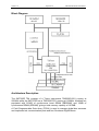
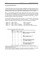
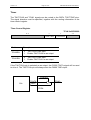
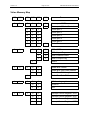
SMT335E
SMT375E
User Manual
User Manual (QCF42); Version 3.0, 5/2/01; © Sundance Multiprocessor Technology Ltd. 2001
Version 1.5
Page 2 of 53
SMT335E SMT375E User Manual
Revision History
Date
Comments
Engineer
Version
04/04/01
Copy from SMT335E V1.1
J.V.
1.0
12/06/02
JTAG Header for FPGA reprogramming added
J.V.
1.1
Y.C
1.2
Interrupt control register 6 address corrected
FPGA firmware version 1.1
24/06/02
SDBC and SDBD Added
FPGA firmware version 1.2
15/07/04
Note about firmware versions added to S.M.
clarify the difference between the 2 versions of
firmware
1.3
21/10/04
Correction in the SDB section
S.M.
1.4
15/04/05
Replace the block diagram
S.M.
1.5
Check your firmware revision number with the program read_version_335E.out and
ask for a more recent version if necessary.
E-mail: [email protected]
.
Version 1.5
Page 3 of 53
SMT335E SMT375E User Manual
Table of Contents
Revision History ....................................................................................................... 2
Contacting Sundance............................................................................................... 5
Notational Conventions ........................................................................................... 6
SMT335E ................................................................................................................ 6
Register Descriptions .............................................................................................. 6
Outline Description .................................................................................................. 7
Block Diagram .......................................................................................................... 8
Architecture Description.......................................................................................... 8
TMS320C6201/6701 .................................................................................................. 9
Boot Mode............................................................................................................... 9
EMIF Control Registers .......................................................................................... 10
SBSRAM............................................................................................................... 10
SDRAM ................................................................................................................. 10
FLASH .................................................................................................................. 10
Reprogramming the firmware and boot code ...................................................... 11
Note about firmware versions ............................................................................... 11
Interrupts................................................................................................................. 12
Interrupt Control Register...................................................................................... 12
Communication ports ............................................................................................ 14
Overview ............................................................................................................... 14
Comm-ports on the SMT335E .............................................................................. 15
Comm-port Status and Control Register ............................................................... 16
Global Status Register .......................................................................................... 19
Data rates ............................................................................................................. 20
SDB .......................................................................................................................... 21
SDB Status Register ............................................................................................. 22
Output Flag Register ............................................................................................. 23
Input Flag Register................................................................................................ 23
SDB update........................................................................................................... 23
SDB Interrupts ...................................................................................................... 24
DMA ...................................................................................................................... 25
Version 1.5
Page 4 of 53
SMT335E SMT375E User Manual
SDB Initialisation................................................................................................... 26
Suspending SDB transmission.............................................................................. 26
Bus exchange ....................................................................................................... 26
SDB Clock selection ............................................................................................. 27
Data formatting ..................................................................................................... 27
Global bus ............................................................................................................... 28
Writing to the Global Bus ...................................................................................... 28
Reading from the Global Bus ................................................................................ 29
Global Bus Operation Register ............................................................................. 30
Global Bus Control Register.................................................................................. 30
PCI access............................................................................................................ 31
Programmable Wait States ................................................................................... 34
Clock Speed ............................................................................................................ 35
LED Setting ............................................................................................................. 35
LED Register......................................................................................................... 35
CONFIG & NMI ........................................................................................................ 36
Config Register ..................................................................................................... 36
Timer........................................................................................................................ 37
Timer Control Register .......................................................................................... 37
Code Composer...................................................................................................... 38
Application Development....................................................................................... 38
Operating Conditions ............................................................................................. 39
Safety.................................................................................................................... 39
EMC ...................................................................................................................... 39
General Requirements .......................................................................................... 39
Power Consumption.............................................................................................. 40
Serial Ports.............................................................................................................. 41
Host Port Interface ................................................................................................. 41
Silicon Serial Number ............................................................................................ 41
C6201 Memory Map ................................................................................................ 42
Flash Access........................................................................................................... 42
Virtex Memory Map................................................................................................. 43
Jumpers................................................................................................................... 45
Version 1.5
Page 5 of 53
SMT335E SMT375E User Manual
JP1: Clock speed select........................................................................................ 45
JP2: Serial port header ......................................................................................... 45
JP3
- Fan power connector ............................................................................... 46
JP4
- External 5V supply ................................................................................... 46
JTAG header ........................................................................................................... 46
SDB Pin-Out ............................................................................................................ 47
Virtex Pin-Out.......................................................................................................... 48
Bibliography............................................................................................................ 51
Index ........................................................................................................................ 52
Contacting Sundance
You can contact Sundance for additional information by sending email to
[email protected]
Version 1.5
Page 6 of 53
SMT335E SMT375E User Manual
Notational Conventions
SMT335E
Throughout this document the term SMT335E will usually be used to refer to both the
SMT335E and the SMT375E. It should be clear from the context when a distinction is
being drawn between the two types of module.
Register Descriptions
The format of registers is described using diagrams of the following form:
31–24
23–16
15–8
7–0
R,00000000
R,10000000
OFLAGLEVEL
R,00000000
RW,10000000
The digits at the top of the diagram indicate bit positions within the register and the
central section names bits or bit fields. The bottom row describes what may be done
to the field and its value after reset. Shaded fields are reserved and should only ever
be written with zeroes.
R
Readable by the CPU
W
Writeable by the CPU
RW
Readable and writeable by the CPU
Binary digits indicate the value of the field after reset.
Version 1.5
Page 7 of 53
SMT335E SMT375E User Manual
Outline Description
The SMT335E is a C6000-based size 2 TIM offering the following features:
SMT335E: TMS320C6201 processor running at 200MHz
SMT375E: TMS320C6701 processor running at 166MHz
Six 20MB/s communication ports
512KB of fast SBSRAM, 16MB of SDRAM
2MB Flash ROM for boot code and FPGA programming
Global expansion connector
High bandwidth data I/O via 4 Sundance Digital Buses (SDB).
Version 1.5
Page 8 of 53
SMT335E SMT375E User Manual
Block Diagram
Architecture Description
The SMT335E TIM consists of a Texas Instruments TMS320C6201 running at
200MHz while the SMT375E has a TMS320C6701 running at 166MHz. Modules are
populated with 512KB of synchronous burst SRAM (SBSRAM) and 16MB of
synchronous DRAM (SDRAM), giving a total memory capacity of 16.5MB.
A Field Programmable Gate Array (FPGA) is used to manage global bus accesses
and implement six communication ports and four Sundance Digital Buses.
Version 1.5
Page 9 of 53
SMT335E SMT375E User Manual
TMS320C6201/6701
Bother processors will run with zero wait states from internal SRAM, the
TMS320C6201 at 200MHz and the TMS320C6701 at 166MHz.
An on-board synthesiser from MicroClock provides the clock used for the C6000;
jumpers on the TIM allow you to select clock speeds from 118MHz to 200MHz.
Unlike similar TIMs based on the TMS320C4x, there is no option to provide an
external clock source.
The TIM configuration feature is fully implemented. This provides a single opencollector line that can be held low until software configuration has been completed.
Boot Mode
The SMT335E is configured to use the following boot sequence each time it is taken
out of reset:
1. The processor copies a bootstrap program from the first 32KB of the flash
memory into internal program RAM starting at address 0.
2. Execution starts at address 0.
The standard bootstrap supplied with the SMT335E then performs the following
operations:
1. All relevant C6000 internal registers are set to default values;
2. The FPGA is configured from data held in flash memory and sets up the
communication ports, the global bus and the Sundance Digital Buses. This
step must have been completed before data can be sent to the comm-ports
from external sources such as the host or other TIMs;
3. A C4x-style boot loader is executed. This will continually examine the six
communication ports until data appears on one of them. The bootstrap will
then load a program in boot format from that port; the loader will not read data
arriving on other ports. See “Application Development” on page 38 for details
of the boot loader format;
4. Finally, control is passed to the loaded program.
Version 1.5
Page 10 of 53
SMT335E SMT375E User Manual
EMIF Control Registers
The C6000 contains several registers that control the external memory interface
(EMIF). There is one global control register and a separate register for each of the
memory spaces CE0 to CE3. A full description of these registers can be found in the
C600001 Peripherals Reference Guide[1].
The standard bootstrap will initialise these registers to the following values:
GC (global control)
0x00003779
0x0000377D
For half speed SBSRAM
For full speed SBSRAM (default)
CE0
0x00000040
Indicates SBSRAM
CE1
0x30FF3F23
Defines asynchronous memory timings
CE2
0x00000030
Indicates SDRAM
CE3
0x00000030
VIRTEX FPGA
SBSRAM
Memory space CE0 is used to access 512KB of zero wait-state SBSRAM over the
C6000 external memory interface (EMI).
SBSRAM is normally set to run at the speed of the C6000 core clock, but the GC
register can be used to reduce this to one half of the core clock speed. The
appropriate setting has to be determined in conjunction with the C6000 core speed
and the external memory speed; refer to Clock Speed on page 35 for further details.
SDRAM
Memory space CE2 is used to access 16MB of SDRAM over the EMI. The SDRAM
operates at one half of the core clock speed.
FLASH
A 2MB Flash ROM device is connected to the C6000 EMI. This device is accessed,
16-bit word at a time, with word addresses from 0x0140 0000 to 0x015F FFFF using
strobe CE1 in 32-bit asynchronous mode. Each 32-bit load will give 16 bits of data in
bits 15–0 of the result; the state of bits 31–16 is undefined.
The ROM holds boot code for the C6000, configuration data for the FPGA, and
optional user-defined code.
A software protection algorithm is in place to prevent programs accidentally altering
the ROM’s contents. Please contact Sundance for further information about reprogramming this device [6].
Version 1.5
Page 11 of 53
SMT335E SMT375E User Manual
Reprogramming the firmware and boot code
The Reprogramming\flash directory of the distribution disk contains a utility that
will run under code composer and program the flash ROM. The utility is called
pflashx_y_z.out, where x_y_z is the FPGA version number.
You load the utility with the code composer “Load Program” option from the “File”
menu. Once the program has loaded, you should select “Run” from the “Debug”
menu. The reprogramming process takes a minute or so and should display “Flash
programming complete” when it has finished. After the program has run you should
“Halt” the processor from the “Debug” menu and select “Run Free”. To confirm that
the programming has been successful you should use the Sundance Server to reset
the board and execute one of the supplied test programs.
A detailed description of the reprogramming process is available as an Application
Note [2], which will also help you to develop your own core in the FPGA.
Note about firmware versions
There are two versions of Sundance firmware for SMT335E.
One version is for the FPGA Virtex-2000. This firmware implements only 2 SDBs,
and it is named: top335ev2000_v1_1.dat
The other version is for the FPGA Virtex-1000. This firmware implements 4 SDBs,
and it is named: top335ev1000_v1_2.dat
Version 1.5
Page 12 of 53
SMT335E SMT375E User Manual
Interrupts
The generation of a CPU interrupt by a comm-port, an SDB, or the Global Bus starts
when the FPGA asserts an interrupt condition. For example, this may be the result of
an input FIFO becoming not empty or an output FIFO not full.
The interrupt condition is then further controlled by interrupt condition enables in the
FPGA. If enabled, an asserted interrupt condition will cause one of the CPU’s
external interrupt lines to be asserted and an interrupt event to be latched in the
processor’s Interrupt Flag Register (IFR).
Finally, the processor will be interrupted, providing the interrupt event is enabled in
the processor’s Interrupt Enable Register (IER) and the Global Interrupt Enable (GIE)
is set in the processor’s Control and Status Register (CSR).
The C6000 provides four external interrupt input lines, EXT_INT4, EXT_INT5,
EXT_INT6, and EXT_INT7, which can be driven by a variety of interrupt conditions.
Each external interrupt has a separate interrupt control register (INTCTRLn) where
you set bits to enable the interrupt condition.
INTCTRL4 0x03E00000
Interrupt Control Register
INTCTRL5 0x03E80000
INTCTRL6 0x03F00000
INTCTRL7 0x03F80000
31–30
29–28
27–26
CP0 IE CP1 IE CP2 IE
RW,00
RW,00
25–24
23–22
21–20
19–18
17–16
CP3 IE
CP4 IE
CP5 IE
SDBA IE
SDBB IE
RW,00
RW,00
RW,00
RW,00
RW,00
RW,00
15
14
13
12
11
10
GB IE
TCLK1 IE
TCLK0 IE
IIOF2 IE
IIOF1 IE
IIOF0 IE
RW,0
RW,0
RW,0
RW,0
RW,0
RW,0
9–0
RW,0000000000
Field
Description
Interrupt condition selected
Version 1.5
Page 13 of 53
SMT335E SMT375E User Manual
CPx IE(bit 0)
Comm-port
Input
Interrupt Enable
FIFO IFBM=0
CPx IE (bit 1)
Comm-port Output
Interrupt Enable
FIFO OFBM=0
SDBx IE (bit 0)
SDB IFLAG Interrupt Enable
≥ IFLAGLEVEL words available
SDBx IE (bit 1)
SDB OFLAG Interrupt Enable
≥ OFLAGLEVEL spaces available
GB IE
Global Bus Interrupt Enable
STAT = 1
TCLKn IE
TIM clock interrupt enable
See TIM specification [3]
IIOFn IE
External line interrupt enable
See TIM specification [3]
IFBM=1
OFBM=1
not empty
8 words available
not full
8 spaces available
It is possible to map more than one condition to an interrupt line. For example, you
might map all of the comm-port conditions to a single interrupt line and then use the
Global Status Register to find which condition or conditions had caused the interrupt.
Version 1.5
Page 14 of 53
SMT335E SMT375E User Manual
Communication ports
Overview
The SMT335E provides six 8-bit, data-parallel, inter-processor links that follow Texas
Instruments’ TMS320C4x Communication Port standard. Additional information on
the standard is available in the TMS320C4x User’s Guide chapter 12:
Communication ports and the Texas Instrument Module Specification.
The standard gives a TIM six links numbered from 0 to 5. Each link can be a
transmitter or a receiver, and will switch automatically between these states
depending on the way you use it. Writing to a receiver or reading from a transmitter
will cause a hardware negotiation (token exchange) that will reverse the state of both
ends of the link.
Following a processor reset, the first three links (0, 1, and 2) initialise as transmitters
and the remainder (3, 4, and 5) initialise as receivers. When you wire TIMs together
you must make sure that you only ever connect links initialising as transmitters to
links initialising as receivers; never connect two transmitters or two receivers. For
example, connecting link 0 of one TIM to link 4 of another is safe; connecting link 0 of
one TIM to link 2 of another could damage the hardware.
Always connect comm-ports 0, 1, or 2 to comm-ports 3, 4, or 5.
On the SMT320 carrier board the physical connection between comm-ports is made
with FMS cables (Ref. SMT3xx-FMS). You must be careful when connecting the
cables the make sure that one end is inserted in the opposite sense to the other. One
end must have the blue backing facing out and the other must have the silver
backing facing out.
The SMT320 motherboard communicates with the host PC using comm-port 3 of the
site 1 TIM. You should not make any other connections to this comm-port.
Version 1.5
Page 15 of 53
SMT335E SMT375E User Manual
Comm-ports on the SMT335E
An SMT335E TIM has access to six FIFO-buffered comm-ports, fully compliant with
the Texas Instruments’ standard [3].
D[0..7]
15x32x2
FIFO
D[0..7]
Address
decode
STRB
RDY
REQ
ACK
… …
Control
Address
15x32x2
FIFO
D[0..7]
15x32x2
STRB
RDY
REQ
ACK
PORT5
Data
STRB
RDY
REQ
ACK
PORT1
FIFO
PORT0
Each comm-port is associated with two 15x32-bit unidirectional FIFOs; one for input
and one for output. An additional one-word buffer makes them appear as 16x32-bit
FIFOs. These allow the guaranteed maximum transfer rate of 20MB/s to be achieved.
Version 1.5
Page 16 of 53
SMT335E SMT375E User Manual
Comm-port Status and Control Register
31–28
CP0_STAT 0x03040000
CP3_STAT 0x031C0000
CP1_STAT 0x030C0000
CP4_STAT 0x03240000
CP2_STAT 0x03140000
CP5_STAT 0x032C0000
27
26
25
24
23–20
19–16
15–12
11-8
IFF
IFE
OFF
OFE
IFL
OFL
R,0
R,1
R,0
R,1
R,0000
R,1111
7
6
5
4
3
2
1
0
ICPRDY
OCPRDY
CLRCP
IFBM
OFBM
CLRIF
CLROF
DIR
R,0
R,1
W,0
RW,0
RW,0
W,0
W,0
R,0
Field
DIR
Description (flags are active when 1)
0
Reading
1
Writing
CLROF
Write 1 to clear outgoing FIFO
CLRIF
Write 1 to clear incoming FIFO
OFBM
Output FIFO Burst Mode
IFBM
Input FIFO Burst Mode
CLRCP
Reset comm-port: Both FIFOs are cleared and the comm-port interface
is set back to its default direction. Use with caution (see below).
OFL
Output FIFO Level: Number of words (0–15) which can be written
OCPRDY
Comm-port interface buffer OCPRDY=’1’ if empty
IFL
Incoming FIFO level: Number of words (0–15) available to be read
ICPRDY
Comm-port interface buffer; ICPRDY=’0’ if empty
OFE
Outgoing FIFO Empty Flag (space is available for writing 16 words)
OFF
Outgoing FIFO Full Flag
IFE
Incoming FIFO Empty Flag
IFF
Incoming FIFO Full Flag (16 words are available to be read)
0
Single-word operation
1
8-word burst mode operation
0
Single-word operation
1
8-word burst mode operation
Version 1.5
Page 17 of 53
SMT335E SMT375E User Manual
There is a control and status register for each of the six comm-ports. There is also
one read-only Global Comm-port Status Register that gathers status from all commports in one place.
Writing
The comm-port output buffer will be loaded with the first word written by the
C6000; the next 15 writes will fill up the output FIFO. When the FIFO is full
OFL will be 0 and OFF will be 1. Any further writes from the C6000 will be
discarded.
Reading
The 15 first words received will fill the input FIFO; the 16th word received will
be kept in the comm-port input buffer. The C6000 can read up to 16 words;
any further read will return an indeterminate value.
Reset
CLRCP should only be used in special applications where the link’s token
exchange has been disabled. This will usually be where the other end of a link
is a device—not another comm-port—that will never attempt to change the
direction of transfer. Damage to the hardware could result if both ends of the
link end up as transmitters.
Clearing the comm-port
The control and status register can be used to discard words in the FIFOs.
Writing a value with CLROF or CLRIF set will clear the selected FIFO; there is
no need to set the bit back to zero.
Note that CLRIF and CLROF clear only the FIFOs; they do not clear the oneword input or output buffers. On input you may need to set CLRIF twice. If the
FIFO is full and a word is in the input buffer, the first CLRIF will clear the FIFO
and allow a word to move in from the input buffer; the second CLRIF will
remove that word. On output you can only clear the output FIFO; any word
already in the output buffer can only be removed by being read from the other
end of the link.
Version 1.5
Page 18 of 53
SMT335E SMT375E User Manual
Interrupts:
The comm-port control logic can assert an interrupt condition as the result of
data being transferred. The condition indicates that either one word or a block
of 8 words has been moved. The bits IFBM and OFBM in the comm-port
control and status register select which condition will assert the interrupt line.
IFBM controls interrupt conditions for input and OFBM for output.
If IFBM=0, the condition will be asserted whenever IFE=0.
If IFBM=1, the condition will be asserted as soon as the input FIFO contains at
least 8 words. The condition will not be asserted again, even if the FIFO
contains 8 or more words, until either of the following events has occurred:
•
8 words have been read from the input FIFO; or
•
A write to an interrupt control register (ICR) has set the associated
Interrupt Enable.
Following one of these events, the condition will be asserted again if or as
soon as the input FIFO contains at least 8 words.
If OFBM=0, the condition will be asserted whenever OFF=0.
If OFBM=1, the condition will be asserted as soon as the output FIFO has
space for 8 or more words. The condition will not be asserted again, even if
the FIFO has space for 8 or more words, until either of the following events
has occurred:
•
8 words have been written to the output FIFO; or
•
A write to an interrupt control register (ICR) has set the associated
Interrupt Enable.
Following one of these events, the condition will be asserted again if or as
soon as the output FIFO contains space for at least 8 words.
Transfer techniques
Transfers can be managed using polling or interrupts, each with CPU control
or DMA. The distribution disk provides programs that demonstrate transfers
and indicate the transfer speeds achieved using these four techniques.
Version 1.5
Page 19 of 53
SMT335E SMT375E User Manual
Global Status Register
STAT 0x033C0000
31–30
29–28
27–26
25–24
23–22
21–20
19–18
17–16
CP0
STAT_INT
CP1
STAT_INT
CP2
STAT_INT
CP3
STAT_INT
CP4
STAT_INT
CP5
STAT_INT
SDBA
STAT_INT
SDBB
STAT_INT
R,10
R,10
R,10
R,10
R,10
R,10
R,10
R,10
15–14
13–12
11–10
9–8
7–6
5–4
3–2
1–0
CP0
STAT
CP1
STAT
CP2
STAT
CP3
STAT
CP4
STAT
CP5
STAT
SDBA
STAT
SDBB
STAT
R,10
R,10
R,10
R,10
R,10
R,10
R,10
R,10
Field
Description (flags active when 1)
CPx STAT(0)
Data available in input FIFO: not(Incoming FIFO Empty Flag)
CPx STAT(1)
Space available in output FIFO: not(Outgoing FIFO Full Flag)
CPx STAT_INT(0)
Input interrupt condition asserted
CPx STAT_INT(1)
Output interrupt condition asserted
The status reflected by STAT_INT depends on the flag settings for the SDBs and the
comm-port burst mode flags, IFBM and OFBM (see comm-port status and control
register).
The Global Status Register is used by the standard boot loader to detect the commport to be used for initial program loading, and is used by interrupt service routines to
detect which link has interrupted in an application using several links simultaneously.
Version 1.5
Page 20 of 53
SMT335E SMT375E User Manual
Data rates
When using the communication links of a C6000 you must remember that the links
share a single bus, so the performance you get will depend on the way you sequence
bus accesses.
C6201 can read at 100MHz from external to internal memory; the rate for the C6701
is 83MHz. If you want to store in external memory then the rate achievable are
divided by two as the read and writes share the same bus, which means respectively
50MHz and 41MHz.
The C6000 DMA channels are not efficient when moving data between two external
memory areas sharing a common bus; the transfer will take place a word at a time
and not in more efficient bursts. This is why it may not be advisable to use DMA to
transfer data directly between external memory and a communication link.
Performance can be greatly improved by using an intermediate buffer in internal
memory.
Version 1.5
Page 21 of 53
SMT335E SMT375E User Manual
SDB
The SMT335E provides four Sundance Digital Buses (SDBs). These 16-bit data
parallel links for synchronous transmission can achieve high-speed data transfer
across 40-way flat ribbon cables with ground-interlaced 3.3v signals (Ref. SMT3xxSDB-CAB).
The SDBs are connected directly to the Virtex device and can support data rates of
up to 200MB/s (100MHz). A total data rate of 800MB/s can be sustained by running
both 16-bit buses at the same time.
An SDB integrates two 256×32-bit unidirectional FIFOs, one for input and one for
output.
256x32x2
FIFO
CLK
WEN
REQ
ACK
D[0..15]
256x32x2
Address
decode
Control
Address Data
Control Logic
& Status
Control Logic
& Status
CLK
WEN
REQ
ACK
SDB A
D[0..15]
SDB B
FIFO
Version 1.5
Page 22 of 53
SMT335E SMT375E User Manual
SDB Status Register
SDBA_STAT 0x03480000
SDBB_STAT 0x03580000
31–30
29
28
27
26
25
24
23–16
IFLAG
OFLAG
IFF
IFE
OFF
OFE
IFL
R,0
R,1
R,0
R,1
R,0
R,1
R,00000000
15–8
7
6
5
OFL
TRANS
PRI
R,11111111
RW,0
RW,0
4
3
2
1
0
DIS
SDBCLK
CLRIF
CLROF
DIR
RW,0
RW,0
W,0
W,0
R,0
Field
Description (flags are active when 1)
DIR
Transfer direction
CLROF
Clear outgoing FIFO
CLRIF
Clear incoming FIFO
SDBCLK
SDB clock speed
DIS
0 Reading
1 Writing
0 50MHz
1 100MHz
0
Pause transmission when FIFO is full
1
Continue transmission even when FIFO full
0
Transmitter wins
1
Equal priority
PRI
Priority for changing direction of transfer
TRANS
Set to 1 after reset to make this SDB start as a transmitter
OFL
Outgoing FIFO Level: number of words that can be written
IFL
Incoming FIFO Level: number of words that can be read
OFE
Outgoing FIFO Empty
OFF
Outgoing FIFO Full
IFE
Incoming FIFO Empty
IFF
Incoming FIFO Full
OFLAG
Outgoing FIFO Flag. Set when OFLAGLEVEL writes can be performed.
IFLAG
Incoming FIFO Flag. Set when IFLAGLEVEL reads can be performed.
Version 1.5
Page 23 of 53
SMT335E SMT375E User Manual
Output Flag Register
SDBA_OUTPUTFLAG 0x034C0000
SDBB_OUTPUTFLAG 0x035C0000
31–24
23–16
15–8
7–0
R,00000000
R,10000000
OTRIGGER
R,00000000
RW,10000000
Input Flag Register
SDBA_INPUTFLAG 0x03440000
SDBB_INPUTFLAG 0x03540000
31–24
23–16
15–8
7–0
ITRIGGER
R,00000000
R,10000000
R,00000000
Field
Description
OTRIGGER
Outgoing FIFO trigger. Set to 128 after reset.
ITRIGGER
Incoming FIFO trigger. Set to 128 after reset.
RW,10000000
OFLAG in the SDB status register will be 1 when there are at least OTRIGGER
spaces available in the output FIFO. OTRIGGER must be programmed with a value
between 1 and 255.
IFLAG in the SDB status register will be 1 when there are at least ITRIGGER words
in the input FIFO. This register must be programmed with a value between 1 and
255.
CLRIF and CLROF do not affect OTRIGGER or ITRIGGER.
SDB update
You should be aware that revisions of the SDB before V3.0.6 have a significantly
different processing of the status flags and a different address is used to program the
SDB flag levels for input and output. When upgrading from versions before V3.0.6,
you will need to change the code for flag programming and accessing the status bits.
You should use version V3.3.6 or above because previous versions could generate
spurious interrupts on input.
Version 1.5
Page 24 of 53
SMT335E SMT375E User Manual
SDB Interrupts
The SMT335E has been designed to allow transfers to be controlled by interrupt
conditions. The main constraint in the design was to make sure that only one
interrupt condition could be generated for each frame of data. This cannot be done
directly by mapping the FIFO flags to interrupt lines because the flags can generate
many edges during a transfer. Instead, after generating an interrupt condition, the
FPGA prevents the device from asserting further conditions until the last address of
the frame has been accessed.
Condition assertion during output:
1. Wait until the output FIFO has enough space to store a new frame, i.e.,
spaces available in the output FIFO >= OTRIGGER.
2. Assert a condition to synchronise a frame transfer (DSP to SDB).
3. Wait until the frame transfer has been completed before looking at the
available space again. Completion is detected by observing a write to the
FIFO at address:
SDB FIFO address + 4*(OTRIGGER–1)
Condition assertion during input:
1. Wait until the input FIFO contains at least one frame, i.e., words available
in the input FIFO >= ITRIGGER.
2. Assert a condition to synchronise a frame transfer (SDB to DSP).
3. Wait until the frame transfer has completed before looking at the number of
words available again. Completion is detected by observing a read from
the FIFO being performed at address:
SDB FIFO address + 4*(ITRIGGER-1)
Writing to IFLAGLEVEL or OFLAGLEVEL will allow the corresponding condition to be
reasserted even though a complete frame transfer may not have happened.
Version 1.5
Page 25 of 53
SMT335E SMT375E User Manual
DMA
SDB transfers can be performed using DMA without any processor interaction.
The DMA should be set to transfer frames of up to 255 words, with read
synchronisation on the SDB’s interrupt condition. The FIFO must be addressed using
consecutive word addresses to allow for correct synchronisation; you must not use
an increment of zero on the DMA’s address into the FIFO. For transfers of more than
one frame, you must use a global index register to adjust the DMA’s address into the
FIFO as follows (note the negative frame index):
SDB OTRIGGER = FRAMESIZE
SDB ITRIGGER = FRAMESIZE
DMA Global Index = (Frame Index<<16) + Element Index
where
Element Index = 4
Frame Index = – 4*(FRAMESIZE-1)
The transfer will access words at offsets in the FIFO from 0 to FRAMESIZE-1.
Applying the negative Frame Index at the end of the frame will bring the offset back
to 0. Accessing the word at offset FRAMESIZE-1 will allow synchronisation by a new
interrupt condition.
The SDB interrupt condition must be mapped in one of the interrupt control registers
to provide synchronisation on one of the external interrupt lines. The first
synchronisation event will be generated when the interrupt control register has been
written and the condition becomes true.
Examples of DMA transfers are provided on the distribution disk.
Version 1.5
Page 26 of 53
SMT335E SMT375E User Manual
SDB Initialisation
The SMT335E SDBs have been designed to allow their use with older, unidirectional
SDBs. When the processor comes out of reset, an SDB will be configured as a
receiver. It can be set to be a transmitter by the DSP, providing the other end of the
bus is not configured as a transmitter.
Initially the SDB clock is stopped; it will start running when the first transfer is
initiated. If the SDB receives 5 clock edges it will be locked as a receiver and will only
become a transmitter as the result of the normal data transfer protocols (using REQ
and ACK signals as described in the SDB specification). As long as the clock lines
are not being driven, the SDB can be switched to a transmitter by setting the TRANS
bit in its control and status register.
When connecting two SDBs together you must make one of them a transmitter
before transfers will work; this is independent of the actual direction of the first
transfer. Neither trying to switch an SDB that has already been connected to a
transmitter nor changing TRANS once the clocks have started running will have any
effect.
When two SMT335E SDBs are connected it does not matter which end is set to be a
transmitter. When connecting an SMT335E to an older, input-only SDB, the
SMT335E SDB must be made a transmitter.
Suspending SDB transmission
To prevent loss of data, transmission will normally be suspended when a receiving
FIFO becomes full. In certain circumstances, allowing the transmission to continue
may be more important than losing data. This can be achieved by setting the DIS bit
in the control and status register.
When DIS is set, a reading SDB will never indicate that its FIFO is full and will
continue reading; a writing SDB will ignore a full signal from the receiver and
continue to send data.
Bus exchange
The SDB allows fully bi-directional transmission but, for maximum throughput, bus
turn-around should be reduced to the minimum. The priority of bus ownership can be
selected using the PRI bit. If PRI is 1 there is no priority: a transmitter will release the
bus as soon as a receiver requests it. If PRI is 0 the transmitter will hold the bus as
long as its output FIFO contains data, even if the receiver is requesting the bus.
Version 1.5
Page 27 of 53
SMT335E SMT375E User Manual
SDB Clock selection
At any time you can change the speed of an SDB clock by altering SDBCLK.
Module
SMT335E
SMT375E
SDBCLK
Clock Speed
0
50MHz
1
100MHz
0
41MHz
1
83MHz
Data formatting
32-bit words are sent in two 16-bit packets with the least significant bits being sent
first.
You should refer to SDB specifications V2.0 and above for technical information [4].
The major change since version V2.0 has been to make the WEN signal active low.
This makes it easy to connect the SDB directly to many types of FIFO and video
processors. All existing boards are compatible with this firmware change without
modification.
Version 1.5
Page 28 of 53
SMT335E SMT375E User Manual
Global bus
The SMT335E provides a global bus that is compatible with the TIM standard. A dual
port RAM (DPR) is used as intermediate storage for transfers of data frames between
the C6000 and an external device on the global bus; each frame can have up to 256
32-bit words. All transfers start from the first word of the DPR. For debugging, the
POS field in the Global Bus Control Register will tell you which word of the frame is
being transmitted.
When writing, the C6000 writes a frame to the DPR and the FPGA then sends it
across the global bus to the external device. When reading, the external device
writes the frame across the global bus to the DPR and the C6000 then reads it.
The FPGA needs to know when the C6000 has finished transferring data to or from
the DPR. It determines this by observing a trigger word in the DPR, usually the final
word of a frame. The FPGA hands control of the DPR to the global bus when the
C6000 accesses the trigger word1. You define the trigger word by setting the
Operation Register TRIGGER field to the number of words in the frame minus one.
A Global Bus Address Register is used to hold the address to be presented to the
external device. You may elect for this address to be incremented by 1 after each
word has been moved between the DPR and the external device; you do this by
setting the INC bit in the Global Bus Control Register.
Writing to the Global Bus
First specify the trigger value in the Operation Register. For example, if your frame
size were 128 words, you would write a trigger value of 127. At the same time that
you set the trigger you must also set the OPERATION bit to 1, indicating that data is
to go from the C6000 to the global bus.
You may now write your data to the DPR. As soon as the FPGA detects a write to the
trigger word, it will send the data in the DPR out to the external device.
Once the complete frame has been sent, the FPGA will signal an interrupt condition
by setting the DONE flag in the Global Bus Control Register. You can use this
condition to interrupt the C6000 or synchronise a DMA transfer.
1
In fact, the actual trigger condition is that bits 9–2 of the address used to access the DPR are equal
to the trigger value. The FPGA ignores bits 17–10 and bits 1–0 of the address used to access the
DPR. This means that there are many trigger locations in the address space allocated to the DPR.
Version 1.5
Page 29 of 53
SMT335E SMT375E User Manual
Reading from the Global Bus
First specify the trigger value in the Operation Register as described above. At the
same time that you set the trigger you must also set the OPERATION bit to 0
indicating that data is to go to the C6000 from the global bus. Setting OPERATION to
0 will start a transfer of data from the external device into the DPR.
As soon as the external device has moved TRIGGER+1 words, the transfer will stop
and the FPGA will set the DONE flag in the Global Bus Control Register, signalling
an interrupt condition. You can use this condition to interrupt the C6000 or
synchronise a DMA transfer.
Once DONE has been set, you may read data out of the DPR. When the FPGA
detects the C6000 reading the trigger word, it will examine the AUTORESTART bit in
the Global Bus Control Register. Another frame transfer from the external device will
start if AUTORESTART is 1; no action will be taken if the bit is 0.
Version 1.5
Page 30 of 53
SMT335E SMT375E User Manual
Global Bus Operation Register
GLOBAL_BUS_LENGTH 0x03900000
31–9
8
7–0
OPERATION
TRIGGER
RW,0
RW,00000000
Field
Description
OPERATION
0
Read from the Global Bus
1
Write to the Global Bus
TRIGGER
One less than the number of words to move
Global Bus Control Register
GLOBAL_BUS_CTRL 0x03800000
31–20
19–16
15–8
WTCNT
RW,0000
7–5
4–3
2
1
0
POS
SWW
INC
AUTORESTART
STAT
R,00000000
RW,00
RW,0
RW,0
R,0
Field
Description
STAT
STAT becomes 1 when a global bus transfer has completed and
is set to 0 when the C6000 next accesses the DPR.
0
The global bus read will only occur when the transfer count
is set.
1
A global bus read operation will be restarted once the
C6000 has read the previous data.
0
Do not increment the address after each transfer.
1
Increment the global bus address after every access
AUTORESTART
INC
SWW
Software wait state mode selection
WTCNT
Number of software wait states (0–15)
POS
Current position of the Global Bus transfer.
Version 1.5
Page 31 of 53
SMT335E SMT375E User Manual
PCI access
You must make sure you know how to configure your carrier board for PCI transfers;
the following example is for the SMT320.
To configure the carrier board for PCI transfers you must write two words to the
global bus:
1
Write to the SMT320 control register (0xC0800000) to select burst
mode or not. In burst mode your transfer size must be a multiple of 16
words;
2
Write the address of your data in the PCI address space to the SMT320
address register (0xC0400000). This address will be incremented by 4
after each word has been transferred.
To start a DMA transfer you have to:
1. Set the DMA destination address to be the SMT320 Dual Port RAM.
2. In the Global bus control register, set auto restart mode if you are reading.
3. Set the DMA to synchronise on one of the INTn lines. For a write operation
you must set the synchronisation event in the DMA secondary control
register; for a read operation you must clear it.
4. Enable the global bus interrupt using the ICR corresponding to the interrupt
line used (see page 38).
5. Set the global bus trigger to be your frame size minus 1.
6. Set a DMA Global Index Register to: (–(FRAME_SIZE<<16)) + 4
7. Start the DMA transfer using the Global Index Register selected above to
control indexing of accesses to the DPR.
The setting of the Global index register is important. With this setting every word
transfer will add 4 to the DMA’s address into the DPR. At the end of each frame, the
negative frame index will bring the address back to the first word of the DPR. This
allows the DMA to access words 0 to 255 of the DPR without ever passing out of the
C6000 address space allocated to it.
Version 1.5
Page 32 of 53
SMT335E SMT375E User Manual
Example of writing a number (size) frames, each of 1024 bytes
int *ptr_gbctrl
= (int *) 0x03800000;
int *ptr_gbstart_addr = (int *) 0x03880000;
int *ptr_gblenth
= (int *) 0x03900000;
int *ptr_gbdpram
= (int *) 0x03A00000;
int *interrupt_reg
= (int *) SMT335EINTCTRL4; // use ext_int4
*interrupt_reg
= 0x00008000;
// Bit 9 sets read or write
// Map GB signal to INT4
// Set SMT320 Burst mode ON
*ptr_gbstart_addr = 0xC0800000;
*ptr_gblenth
= 0+0x100;
*ptr_gbdpram
= 0x00000001;
// Write command of 1 word
while(((*ptr_gbctrl)&0x1)==0) {}
// Set the SMT320 PCI address destination
*ptr_gbstart_addr = 0xC0400000;
*ptr_gblenth
= 0+0x100;
// Write command
*ptr_gbdpram
= addr;
// PCI destination address
// Send the data over the PCI
*ptr_gbstart_addr = 0xC0000000;
*DMA_PRI_CRTL0
= 0x070100F0;
// Set interrupt sources INT4
*DMA_SEC_CRTL0
= 0x00009000;
// Set the first interrupt
*ptr_gblenth
= 256-1+0x100;
// multiple of 16 in burst mode
*DMA_SRC_ADDR0
= (int)ptr_buffer;
// Set the source address
*DMA_DST_ADDR0
= (int)ptr_gbdpram; // Set the destination address
*DMA_XFR_CNTR0
= (size<<16)+0x100; // Set the transfer sizes
// FRAME_CNT= size, E_CNT=0x0100
*DMA_GL_CNT_RLD
= 0x0100;
// Set the count reload
DMA_GL_INDEX
= ((-255*4)<<16)+4; // index: Frame
= –255*4 bytes
// index: Element = 4 bytes
*DMA_PRI_CRTL0
= 0x070100D1;
// Start DMA0 using INT4
// Use index only for destination
while((*DMA_PRI_CRTL0&0xc)!=0) {}
// Wait for DMA1 to finish
while(((*ptr_gbctrl)&0x1)==0) {}
// Complete final write
*interrupt_reg = 0;
// Clear INTCTRL4
Version 1.5
Page 33 of 53
SMT335E SMT375E User Manual
Example of reading a number (size) frames, each of 1024 bytes
int *ptr_gbctrl
=(int*) 0x03800000;
int *ptr_gbstart_addr =(int*) 0x03880000;
int *ptr_gblenth
=(int*) 0x03900000;
int *ptr_gbdpram
=(int*) 0x03A00000;
int *interrupt_reg
=(int *) SMT335EINTCTRL4; // use ext_int4
*interrupt_reg
= 0x00008000;
// Bit 9 sets read or write
// Map GB signal to INT4
// Set SMT320 Burst mode ON
*ptr_gbstart_addr = 0xC0800000;
*ptr_gblenth
= 0+0x100;
*ptr_gbdpram
= 0x00000001;
// Write command of 1 word
while(((*ptr_gbctrl)&0x1)==0) {}
// Set the SMT320 PCI address destination
*ptr_gbstart_addr = 0xC0400000;
*ptr_gblenth
= 0+0x100;
// Write command
*ptr_gbdpram
= addr;
// PCI destination address=addr
// Send the data over the PCI
*ptr_gbstart_addr = 0xC0000000;
*DMA_PRI_CRTL0
= 0x070100F0;
// Set interrupt sources INT4
*DMA_SEC_CRTL0
= 0x0000A000;
// Clear the interrupt
*ptr_gbctrl
= 2;
// auto-reload no address inc
*ptr_gblenth
= 256-1+0x100;
// multiple of 16 in burst mode
*DMA_SRC_ADDR0
= (int)ptr_gbdpram; // Set the source address
*DMA_DST_ADDR0
*DMA_XFR_CNTR0
= (int)ptr_buffer; // Set the destination address
= (size<<16)+0x100; // Set the transfer sizes
// FRAME_CNT = size, E_CNT=0x0100
*DMA_GL_CNT_RLD
= 0x0100;
// Set the count reload
*DMA_GL_INDEX
= ((-255*4)<<16)+4; // index: Frame
= –255*4 bytes
// index: Element = 4 bytes
*DMA_PRI_CRTL0
= 0x07010071;
// Start DMA0 using INT4
// Use index only for source
while((*DMA_PRI_CRTL0&0xc)!=0) {}
// Wait for DMA1 to finish
*interrupt_reg
// Clear INTCTRL4
= 0;
Version 1.5
Page 34 of 53
SMT335E SMT375E User Manual
Programmable Wait States
The SMT335E has its own internal software-configurable wait-state generator that is
used in conjunction with the external ready line, RDY. You control the generator by
configuring two fields in the Global Bus Control Register: WTCNT specifies the
number of software wait states to generate and SWW selects one of four options.
RDYwtcnt is an internally generated ready signal. When an external access is begun,
the value WTCNT is loaded into a counter; WTCNT can be any value from 0 through
15. The counter is decremented every H1/H3 clock cycle until it becomes 0. Once the
counter reaches 0, it will remain at 0 until the next external access. RDYwtcnt will be 1
while the counter is nonzero and 0 otherwise.
The four SWW options combine RDY and RDYwtcnt to generate the internal ready
signal, RDYint that controls accesses. As long as RDYint = 1, the current external
access is extended. When RDYint becomes 0, the current access will complete.
SWW = 002
SWW = 012
SWW = 102
SWW = 112
RDYint = RDY;
RDYint = RDYwtcnt;
RDYint = RDYwtcnt OR RDY;
RDYint= RDYwtcnt AND RDY;
RDYwtcnt is ignored.
RDY is ignored.
either generates ready.
both must occur to generate ready.
Additional information is available in the TMS320C4x User’s Guide [5] chapter 9.4:
Programmable Wait States.
Note that bus sharing is supported in firmware versions 2.5 and above. The global
bus lines will be tri-stated according to the state of the AE, DE and CE lines.
Version 1.5
Page 35 of 53
SMT335E SMT375E User Manual
Clock Speed
You must consider EMIF device speeds when choosing the appropriate C6000 clock
speed. Under most circumstances, the C6201 would be set to 200MHz and have an
SBSRAM speed equal to the core speed; the C6701 would be set to 166MHz. See
the description of jumper JP1 on page 45.
C6000 clock
SBSRAM
SDRAM
FPGA
133
166
200
200
133
166
100
200
67
83
100
100
67
83
100
100
LED Setting
The SMT335E has 7LEDs.
The LEDs 1 to 4 can be controlled with the LED register. Writing 1 will illuminate the
LED; writing 0 will turn it off.
LED 5 always displays the state of the FPGA DONE pin. This LED is off when the
FPGA is configured (DONE=1) and on when it is not configured (DONE=0). This LED
should go on when the board is first powered up and go off when the FPGA has been
successfully programmed. If it stays on, the DSP is not booting correctly. It should go
on and off at every reset.
The LED 6 is showing the 3.3V power supply. It should be on. If not check that you
have the mounting pillars and screws fitted properly.
The LED 7 is showing the Virtex core power supply. It should be on.
LED Register
LED 0x03D00000
31–4
3
2
1
0
LED 4
LED 3
LED 2
LED 1
RW,0
RW,0
RW,0
RW,0
Version 1.5
Page 36 of 53
SMT335E SMT375E User Manual
CONFIG & NMI
The TIM specification describes the operation of an open-collector type signal
CONFIG that is driven low after reset.
This signal, on a standard C4x based TIM, is connected to the processor’s IIOF3 pin.
On the SMT335E/375, the CONFIG signal is asserted after power on, and can be
released by writing the value (1<<7) to the config register. Conversely, CONFIG may
be re-asserted by writing 0 to this bit. It is not possible for software to read the state
of the CONFIG signal.
The NMI signal from the TIM connector can be routed to the C6000 NMI pin.
WARNING: Several software components include code sequences that assume
setting GIE=0 in the C6000 CSR will inhibit all interrupts; NMI violates that
assumption. If an NMI occurs during such code sequences it may not be safe to
return from the interrupt. This may be particularly significant if you are using the
compiler’s software pipelining facility.
Config Register
TIMCONFIG 0x03C80000
31–8
Field
TRICONF
NMIEN
7
6
NMI EN
TRI CONF
RW,0
RW,0
Description
0
drive CONFIG low
1
tri-state CONFIG
0
Disconnect NMI from the C6000
1
Connect NMI from TIM to the C6000.
5–0
Version 1.5
Page 37 of 53
SMT335E SMT375E User Manual
Timer
The TIM TCLK0 and TCLK1 signals can be routed to the DSP’s TOUT/TINP pins.
The signal direction must be specified, together with the routing information in the
timer control register.
Timer Control Register
TCLK 0x03C00000
31–6
Field
5
4
TCLK1 EN
TCLK9 EN
RW,0
RW,0
3–0
Description
TCLK0EN
TCLK1EN
0
TIM TCLK0 is an input
1
Enable TIM TCLK0 as an output
0
TIM TCLK1 is an input
1
Enable TIM TCLK1 as an output
If the TIM TCLKx pin is selected as an output, the C6000 TOUTx signal will be used
to drive it. The TIM TCLKx pin will always drive the C6000 TINPx input.
TCLK0EN
C6x
TOUT0
TCLK0
TINP0
FPGA
Version 1.5
Page 38 of 53
SMT335E SMT375E User Manual
Code Composer
This module is fully compatible with the Code Composer debug environment. This
extends to both the software and JTAG debugging hardware including the
SMT320V4, SMT327, SMT328 and TI’s XDS-510.
Application Development
You can develop code for SMT335E/375 modules in several ways. The simplest is to
use the Sundance SMT6000 Server Loader and its associated libraries.
The Server Loader is an application that runs on a host PC under either Windows 98
or NT and allows you to run COFF-format applications. Modified forms of the TI rts
library, one for the C6201 and one for the C6701, support standard C I/O.
The Server Loader will read a .out file and convert it into C4x-style boot code which
is then transmitted down a comm-port to the SMT335E.
The boot code is in the following format:
Word2 1
6-word
header
Load Block
0x00003779
half speed SBSRAM
0x0000377D
full speed SBSRAM (recommended)
Words 2, 3, 4
0, 0, 0
Word 5
start address
Word 6
0
Word 1
4*N: Length of load block (in bytes)3
Word 2
Destination address (external memory only)
Next N words
N data words
Word 1
04
0 or more
Load Blocks
Terminator
2
A word is 32 bits
3
The length of each data block will be rounded up to a multiple of 4 bytes if necessary.
4
Effectively a zero-length Load Block
Version 1.5
Page 39 of 53
SMT335E SMT375E User Manual
Operating Conditions
Safety
The module presents no hazard to the user.
EMC
The module is designed to operate within an enclosed host system that provides
adequate EMC shielding. Operation within the EU EMC guidelines is only guaranteed
when the module is installed within an appropriate host system.
The module is protected from damage by fast voltage transients introduced along
output cables from outside the host system.
Short-circuiting any output to ground does not cause the host PC system to lock up
or reboot.
General Requirements
The module must be fixed to a TIM40-compliant carrier board.
The SMT335E TIM is in a range of modules that must be supplied with a 3.3v power
source. In addition to the 5v supply specified in the TIM specification, these new
generation modules require an additional 3.3v supply to be presented on the two
diagonally-opposite TIM mounting holes. The lack of this 3.3v power supply should
not damage the module, although it will obviously be inoperable; prolonged operation
under these circumstances is not recommended.
This module is not directly compatible with earlier generations of TIM motherboards,
although the 3.3v supply can be provided from a separate source. It is, however,
compatible with the latest generation of Sundance TIM carrier boards such as the
SMT320V4 and subsequent versions (PCI), and SMT328 (VME), which present the
3.3v via conductive mounting pillars.
Use of the TIM on SMT327 (cPCI) motherboards may require a firmware upgrade. If
LED #1 on the SMT335E remains illuminated once the TIM is plugged in and
powered up, the SMT327 needs the upgrade. The latest firmware is supplied with all
new boards shipped. Please contact Sundance directly if you have an older board
and need the upgrade.
A SMT320V3 motherboard can be used providing a SMT335E TIM is not located in
the first slot; putting one there prevents the SMT320V3 from coming out of reset. Any
other type of TIM must be placed in the first slot of this motherboard to ensure correct
operation.
The external ambient temperature must remain between 0°C and 40°C, and the
relative humidity must not exceed 95% (non-condensing).
Version 1.5
Page 40 of 53
SMT335E SMT375E User Manual
Power Consumption
The power consumption of this TIM is dependent on the operating conditions in terms
of core activity and I/O activity. The figures will be added to the document.
Version 1.5
Page 41 of 53
SMT335E SMT375E User Manual
Serial Ports
The C6000 contains two multichannel buffered serial ports (McBSP). The signals
involved are connected to a 0.1” pitch DIL pin header (JP2). For a full description of
signal activity and the serial protocols available, please refer to Chapter 11 of [1].
Signal
Pin
Pin
Signal
FSX1
1
2
FSX0
FSR1
3
4
FSR0
DX1
5
6
DX0
DR1
7
8
DR0
CLKX1
9
10
CLKX0
CLKR1
11
12
CLKR0
CLKS1
13
14
CLKS0
GND
15
16
GND
The ‘C6x serial ports are connected directly to the Virtex FPGA and a 2mm pitch DIL
pin header. No functionality is provided as standard within the Virtex.
Note that it can be used as additional interrupt sources to the DSP.
Host Port Interface
The ‘C6x host port interface (HPI) is connected directly to the Virtex FPGA. No
functionality is provided as standard within the Virtex.
Silicon Serial Number
The Virtex is connected directly to a Dallas Semiconductor DS2430 silicon serial
number devices. It will output a unique 64 bit serial number, and therefore this can be
used as a protection mechanism to any cores that need to be protected. The device
includes 256 bits of EEPROM.
Version 1.5
Page 42 of 53
SMT335E SMT375E User Manual
C6201 Memory Map
Starting Address
RESOURCE
00000000
Internal Program RAM
00010000
Reserved
00400000 – 0047FFFF
01400000 – 015FFFFF
External Memory Space CE0
512KB SBSRAM
External Memory Space CE1
2MB Flash
01800000
Internal Peripherals
01C00000
Reserved
02000000 -02FFFFFF
03000000 – 03FFFFFF
Refer to
External Memory Space CE2
16MB SDRAM
SBSRAM
Flash
SDRAM
External Memory Space CE3
Comm-ports,
See Virtex memory map
SDB, Global bus
04000000
Reserved
80000000
Internal Data RAM
80010000
Reserved
80400000
Reserved
Flash Access
Address
01400000 – 015FFFFF
Resource
ED31
ED30
CE1
0
0
Read Flash / Write Flash
0
1
Read Flash / Pulse PROG
1
0
Read Flash / Write CCLK
1
1
Read Flash / Write Flash
Version 1.5
Page 43 of 53
SMT335E SMT375E User Manual
Virtex Memory Map
A23
A22
A21
A20
A19
A18
0
0
0
0
0
0
Comm port 0 FIFO
1
Comm port 0 Status/Control
0
0
0
1
Comm port 1
0
1
0
Comm port 2
0
1
1
Comm port 3
1
0
0
Comm port 4
1
0
1
Comm port 5
1
1
1
1
Global Status
0
0
0
SDB A FIFO
0
1
SDB A Input Flag
1
0
SDB A Status/Control
1
1
SDB A Output Flag
1
1
1
0
0
SDB B
0
0
Global Bus Control
0
1
Global Bus DMA Start Address
1
0
Global Bus DMA Length
1
1
1
1
1
Resource
0
1
Global Bus Data RAM
0
0
TCLK routing register
0
1
CONFIG
1
0
LED
0
0
Interrupt Control Register, INT4
0
1
Interrupt Control Register, INT5
1
0
Interrupt Control Register, INT6
1
1
Interrupt Control Register, INT7
Version 1.5
Page 44 of 53
SMT335E SMT375E User Manual
The memory mapping is available in SMT335E.h as follows:
#define SMT335ECP0
(volatile unsigned int *)0x03000000
#define SMT335ECP1
(volatile unsigned int *)0x03080000
#define SMT335ECP2
(volatile unsigned int *)0x03100000
#define SMT335ECP3
(volatile unsigned int *)0x03180000
#define SMT335ECP4
(volatile unsigned int *)0x03200000
#define SMT335ECP5
(volatile unsigned int *)0x03280000
#define SMT335ECP0_STAT
(volatile unsigned int *)0x03040000
#define SMT335ECP1_STAT
(volatile unsigned int *)0x030C0000
#define SMT335ECP2_STAT
(volatile unsigned int *)0x03140000
#define SMT335ECP3_STAT
(volatile unsigned int *)0x031C0000
#define SMT335ECP4_STAT
(volatile unsigned int *)0x03240000
#define SMT335ECP5_STAT
(volatile unsigned int *)0x032C0000
#define SMT335ESTAT
(volatile unsigned int *)0x033C0000
#define SMT335ESDBA
(volatile unsigned int *)0x03400000
#define SMT335ESDBB
(volatile unsigned int *)0x03500000
#define SMT335ESDBA_STAT
(volatile unsigned int *)0x03480000
#define SMT335ESDBB_STAT
(volatile unsigned int *)0x03580000
#define SMT335ESDBA_INPUTFLAG
(volatile unsigned int *)0x03440000
#define SMT335ESDBB_ INPUTFLAG
(volatile unsigned int *)0x03540000
#define SMT335ESDBA_OUTPUTFLAG
(volatile unsigned int *)0x034C0000
#define SMT335ESDBB_OUTPUTFLAG
(volatile unsigned int *)0x035C0000
#define SMT335ESDBC
(volatile unsigned int *)0x03600000
#define SMT335ESDBD
(volatile unsigned int *)0x03700000
#define SMT335ESDBC_STAT
(volatile unsigned int *)0x03680000
#define SMT335ESDBD_STAT
(volatile unsigned int *)0x03780000
#define SMT335ESDBC_INPUTFLAG
(volatile unsigned int *)0x03640000
#define SMT335ESDBD_ INPUTFLAG
(volatile unsigned int *)0x03740000
#define SMT335ESDBC_OUTPUTFLAG
(volatile unsigned int *)0x036C0000
#define SMT335ESDBD_OUTPUTFLAG
(volatile unsigned int *)0x037C0000
#define GLOBAL_BUS
(volatile unsigned int *)0x03A00000
#define GLOBAL_BUS_CTRL
(volatile unsigned int *)0x03800000
#define GLOBAL_BUS_START
(volatile unsigned int *)0x03880000
#define GLOBAL_BUS_LENGTH
(volatile unsigned int *)0x03900000
#define SMT335ETCLK
(volatile unsigned int *)0x03C00000
#define SMT335ETIMCONFIG
(volatile unsigned int *)0x03C80000
#define SMT335ELED
(volatile unsigned int *)0x03D00000
#define SMT335EINTCTRL4
(volatile unsigned int *)0x03E00000
#define SMT335EINTCTRL5
(volatile unsigned int *)0x03E80000
#define SMT335EINTCTRL6
(volatile unsigned int *)0x03F00000
#define SMT335EINTCTRL7
(volatile unsigned int *)0x03F80000
Version 1.5
Page 45 of 53
SMT335E SMT375E User Manual
Jumpers
JP1: Clock speed select
S2
S1
S0
C6000 CLK
(MHz)
IN
IN
IN
200
IN
IN
OUT
182
IN
OUT
IN
167
IN
OUT
OUT
154
OUT
IN
IN
143
OUT
IN
OUT
133
OUT
OUT
IN
125
OUT
OUT
OUT
118
S0, S1 and S2 refer to the following link positions
on JP1.
S2 S1 S0
JP2: Serial port header
Refer to the TMS320C6201 Peripheral Reference Guide [1] for a description of the
signals and their usage.
2
4
6
8
10
12
14
16
FSX0
FSR0
DX0
DR0
CLKX0
CLKR0
CLKS0
GND
FSX1
FSR1
DX1
DR1
CLKX1
CLKR1
CLKS1
GND
1
3
5
7
9
11
13
15
Version 1.5
JP3
-
Page 46 of 53
SMT335E SMT375E User Manual
Fan power connector
This connector supplies 5V DC power for the Virtex cooling fan.
JP4
-
External 5V supply
This connector (standard disk drive connector) is used to supply additional 5V power
to the module.
JTAG header
The FPGA can be directly reprogrammed via Xilinx JTAG parallel cable III.
The pinout is the following:
JP9
1
4
2
5
3
6
1: Vcc 3.3V
2: Gnd
3: TCK (FPGA pin E29)
4: TDI (FPGA pin D5)
5: TMS (FPGA pin B33)
6: TDO (FPGA pin E6)
Version 1.5
Page 47 of 53
SMT335E SMT375E User Manual
SDB Pin-Out
Pin
Signal
Signal
Pin
1
CLK
GND
2
3
D0
GND
4
5
D1
GND
6
7
D2
GND
8
9
D3
GND
10
11
D4
GND
12
13
D5
GND
14
15
D6
GND
16
17
D7
GND
18
19
D8
GND
20
21
D9
GND
22
23
D10
GND
24
25
D11
GND
26
27
D12
GND
28
29
D13
GND
30
31
D14
GND
32
33
D15
GND
34
35
UD0
DIR
36
37
WEN
REQ
38
39
UD1
ACK
40
Version 1.5
Page 48 of 53
SMT335E SMT375E User Manual
Virtex Pin-Out
A17
SDBB_CLK_BG
C25
SDBD_DATA<8>
C18
SDBB_DATA<0>
C12
C5P<10>
A27
D24
SDBD_DATA<7>
E18
NRESET
E13
C5P<0>
B25
E23
SDBD_DATA<10>
D17
CLKEXT
A11
C5P<1>
C28
A25
SDBD_DATA<9>
A3
C3P<6>
D12
C5P<2>
C30
SP2_DR
D23
SDBD_DATA<12>
D9
C4P<4>
B11
C5P<8>
D30
SP2_CLKR
B24
SDBD_DATA<11>
E8
C3P<1>
C11
C5P<9>
E28
SP2_CLKX
E22
E11
C5P<7>
B10
C5P<3>
D29
SP2_CLKS
C23
SDBD_DIR
E17
SDBB_CLK_IO
D11
C5P<4>
D28
SP2_DX
A23
SDBD_DATA<14>
A19
SDBB_DATA<10>
C10
C5P<5>
A31
SP2_FSR
D22
SDBD_DATA<13>
D18
SDBB_DATA<9>
A9
C5P<6>
E27
SP2_FSX
E21
SDBB_DATA<2>
B16
SDBB_DATA<12>
C9
C4P<0>
B22
SDBB_DATA<1>
D16
SDBB_DATA<11>
D10
C4P<1>
C29
B30
SDBD_DATA<2>
D21
SDBD_U0
E16
SDBB_DATA<14>
A8
C4P<2>
D27
SDBD_DATA<1>
C21
SDBD_DATA<15>
C16
SDBB_DATA<13>
B8
C4P<3>
E26
SDBD_DATA<4>
B21
SDBB_DATA<4>
A15
E10
C4P<9>
B29
SDBD_DATA<3>
E20
SDBB_DATA<3>
C15
SDBB_DIR
C8
C4P<8>
D26
SDBD_DATA<6>
D20
SDBB_DATA<6>
D15
SDBB_U0
B7
C4P<5>
C27
SDBD_DATA<5>
C20
SDBB_DATA<5>
E15
SDBB_DATA<15>
A6
C4P<6>
E25
SDBD_ACK
B20
C14
SDBB_U1
C7
C4P<7>
A28
SDBD_REQ
E19
D14
SDBB_WEN
D8
C4P<10>
D25
SDBD_DATA<0>
D19
SDBB_DATA<8>
A13
SDBB_ACK
A5
C4P<11>
C26
SDBD_CLK_IO
C19
SDBB_DATA<7>
E14
SDBB_REQ
B5
C3P<0>
A17
SDBB_CLK_BG
C25
SDBD_DATA<8>
C12
C5P<10>
A27
W5
ED<12>
E13
C5P<0>
A4
C3P<8>
J5
NBE<1>
P2
EA<17>
Y3
ED<11>
B4
C3P<9>
F1
NBE<2>
R5
EA<16>
Y4
ED<10>
C5
C3P<4>
J4
ED<31>
R4
NRAS
AA1
ED<9>
E7
C3P<5>
H3
ED<30>
R3
NSDRAMWE
Y5
ED<8>
D6
C3P<7>
K5
ED<29>
R1
NSDRAMCS
AA3
ED<7>
A2
C3P<10>
H2
ED<28>
T4
NCAS
AA4
ED<6>
J3
ED<27>
T5
EA<15>
AB3
ED<5>
K4
ED<26>
T3
EA<14>
AA5
ED<4>
D3
F3
DMAC<0>
Version 1.5
Page 49 of 53
SMT335E SMT375E User Manual
G1
NBE<3>
L5
ED<24>
T2
EA<13>
AC1
ED<3>
J2
ED<25>
K3
ED<23>
U3
EA<12>
AB4
ED<2>
D4
L4
ED<22>
AE3
LED<4>
AC3
ED<1>
E4
K2
ED<21>
AF3
INT5
AB5
ED<0>
M5
ED<20>
AH3
NTIMNMI
AC4
B3
L3
ED<19>
AK3
C0P<0>
AD3
F4
L1
ED<18>
U1
EA<10>
AE1
F5
C3P<11>
C1
ARDY
M4
ED<17>
U2
EA<9>
AC5
LED<5>
G5
NAWE
N5
ED<16>
V2
EA<8>
AD4
LED<3>
E3
NAOE
M2
ED<15>
V4
EA<7>
AF1
LED<2>
D2
NARE
N4
ED<14>
V5
EA<6>
AF2
NC60NMI
G4
NLOCK
N3
ED<13>
V3
EA<5>
AD5
NC60IACK
H5
DMAC<1>
N2
EA<21>
W1
EA<4>
AG2
INT7
E2
DMAC<2>
P5
EA<20>
W3
EA<3>
AE4
INT6
A4
C3P<8>
J5
NBE<1>
P2
EA<17>
Y3
ED<11>
B4
C3P<9>
F1
NBE<2>
R5
EA<16>
Y4
ED<10>
AF4
IIOF1
AM4
C0P<10>
AK13
SDBA_WEN
AJ18
SDBA_DATA<8>
AJ1
IIOF0
AM5
C0P<11>
AL13
SDBA_U1
AN19
SDBA_DATA<5>
AJ2
CONFIG
AK7
C0P<7>
AM13
SDBA_REQ
AL19
SDBA_DATA<6>
AF5
NTIMIACK
AL6
C1P<10>
AN13
SDBA_ACK
AK18
SDBA_DATA<7>
AG4
TCLK0
AM6
C1P<7>
AJ14
SDBA_DATA<15>
AM18
SDBA_DATA<0>
AK2
TCLK1
AN6
C1P<6>
AK14
SDBA_U0
AJ19
SDBA_DATA<3>
AJ3
TOUT1
AL7
C1P<5>
AM14
SDBA_DATA<13>
AL20
SDBA_DATA<4>
AG5
TOUT0
AJ9
C1P<4>
AN15
SDBA_DATA<14>
AN21
SDBA_DATA<1>
AL1
TIN1
AN7
C1P<3>
AJ15
SDBA_DIR
AL21
SDBA_DATA<2>
AH4
TIN0
AL8
C1P<9>
AK15
AJ20
SDBC_DATA<15>
AJ4
C0P<1>
AM8
C1P<2>
AL15
SDBA_DATA<11>
AM22
SDBC_U0
AJ10
C1P<1>
AM16
SDBA_DATA<12>
AK21
SDBC_DATA<13>
AH5
U4
EA<11>
AL9
C1P<0>
AL16
SDBA_DATA<9>
AN23
SDBC_DATA<14>
AL17
CLK100
AM9
C2P<11>
AJ16
SDBA_DATA<10>
AJ21
SDBC_DATA<11>
AJ8
C1P<11>
AK10
C2P<10>
AK16
AM23
SDBC_DATA<12>
AJ11
C2P<6>
AN9
C2P<7>
AN17
AK22
SDBC_REQ
AK6
C0P<8>
AL10
C2P<5>
AM17
SDBA_CLK_IO
AM24
SDBC_ACK
AK9
C1P<8>
AM10
C2P<4>
AJ17
SDBA_CLK_BG
AL23
SDBC_DATA<9>
AL4
C0P<2>
AL11
C2P<9>
AL25
AJ22
SDBC_DATA<10>
Version 1.5
Page 50 of 53
SMT335E SMT375E User Manual
AJ6
C0P<3>
AJ12
C2P<8>
AL28
HPINDS2
AK23
SDBC_CLK_IO
AK5
C0P<4>
AN11
C2P<3>
AL30
HPID<3>
AL24
SDBC_DATA<0>
AN3
C0P<9>
AK12
C2P<2>
AN28
AN26
SDBC_DIR
AF4
IIOF1
AM4
C0P<10>
AK13
SDBA_WEN
AJ18
AJ1
IIOF0
AM5
C0P<11>
AL13
SDBA_U1
AN19
AM26
SDBC_U1
AK31
HPID<6>
AC33
GBD<12>
G30
GBA<30>
AM27
SDBC_DATA<7>
AH30
HPID<7>
AB30
GBD<13>
K30
GBA<16>
AJ24
SDBC_DATA<8>
AG29
HPID<9>
AB31
GBD<14>
U31
STAT<1>
AL26
SDBC_DATA<5>
AJ31
HPID<10>
AA29
GBD<15>
U32
STAT<2>
AK25
SDBC_DATA<6>
AK32
HPID<11>
AA30
NGBDE
T32
STAT<3>
AN29
SDBC_DATA<3>
AG30
HPID<12>
AA31
GBD<16>
T30
H3
AJ25
SDBC_DATA<4>
AH31
HPID<13>
AA32
GBD<17>
T29
H1
AK26
SDBC_DATA<1>
AF29
HPID<14>
Y29
GBD<18>
T31
NTIMRDY
AM29
SDBC_DATA<2>
AH32
HPINBE<1>
AA33
GBD<19>
R33
NTIMSTRB1
AM30
HPININT
AF30
HPINBE<0>
Y30
GBD<20>
R31
NGBCE1
AJ26
HPINRDY
AE29
HPINAS
Y32
GBD<21>
R30
TIMPAGE1
AK27
HPINDS1
AH33
HPIHWIL
W29
GBD<22>
R29
NTIMRW1
AL29
HPINCS
AG33
HPICNTL<1>
W30
GBD<23>
P32
STAT<0>
AN31
HPIR
AE30
HPICNTL<0>
W31
GBD<24>
P31
GBA<0>
AJ27
HPID<0>
AD29
GBD<1>
W33
GBD<25>
P30
GBA<1>
AM31
HPID<1>
AF32
GBD<2>
V30
GBD<26>
P29
GBA<2>
AK28
HPID<2>
AE31
GBD<3>
V29
GBD<27>
M32
GBA<3>
AD30
GBD<4>
V31
GBD<28>
N31
GBA<4>
AL18
AE33
GBD<7>
AE32
GBD<5>
V32
GBD<29>
N30
GBA<5>
AF31
GBD<0>
AC29
GBD<6>
U33
GBD<30>
L33
GBA<6>
AJ32
HPID<15>
AD31
GBD<8>
U29
GBD<31>
M31
GBA<7>
AL33
HPID<8>
AC30
GBD<9>
E30
SP1_FSX
L32
GBA<8>
AM26
SDBC_U1
AK31
HPID<6>
AC33
GBD<12>
G30
GBA<30>
AH30
HPID<7>
AB30
GBD<13>
K30
GBA<16>
U31
STAT<1>
AM27
Comm ports are numbered C0 to C5. Each has 12 elements (i.e. CnP[0..11]).
CnP0 = STRB, CnP1 = RDY, CnP2 = REQ, CnP3 = ACK, CnP[4..11] = Data[0..7].
Version 1.5
Page 51 of 53
SMT335E SMT375E User Manual
Bibliography
1. TMS320C6201/C6701 Peripherals Reference Guide (literature number
SPRU190) describes common peripherals available on the TMS320C6201/C6701 digital signal
processors. This book includes information on the internal data and program memories, the
external memory interface (EMIF), the host port, multichannel-buffered serial ports, direct memory
access (DMA), clocking and phase-locked loop (PLL), and the power-down modes.
2.
3.
4.
5.
Application Note: Flash Programming
TIM-40 MODULE SPECIFICATION Including TMS320C44 Addendum
SDB Technical Specification V2.1 or above
TMS320C4x User's Guide (literature number SPRU063) describes the C4x 32-bit
floating-point processor, developed for digital signal processing as well as parallel processing
applications. Covered are its architecture, internal register structure, instruction set, pipeline,
specifications, and operation of its six DMA channels and six communication ports. Software and
hardware applications are included.
6. Application Note: Creating New Firmware
Version 1.5
Page 52 of 53
SMT335E SMT375E User Manual
Index
Application Development...............38
server-loader.................................38
Architecture Description..................8
Bibliography....................................51
Block Diagram ..................................8
Board not working
badly-connected comports ............14
field values after reset..................... 6
Flash ............................................... 10
access .......................................... 42
comport reset misused..................17
protection algorithm...................... 10
FPGA................................................. 8
configuration................................... 9
Global Bus...................................... 28
control register ............................. 30
firmware revision.............................2
DMA Global Index Register.......... 31
LED 1 illuminated..........................35
example of reading....................... 33
NMI ...............................................36
example of writing ........................ 32
no 3.3v supply...............................39
operation register ......................... 30
no SDB transmitter selected .........26
PCI access ................................... 31
old version of SDB ........................23
boot code format ............................38
Boot Mode .........................................9
bootstrap program ...........................9
carrier boards .................................39
Clock
speed ............................................35
reading ......................................... 29
writing........................................... 28
Input Flag Register ........................ 23
Interrupts ........................................ 12
asserting....................................... 18
enabling ....................................... 12
speed select.................See Jumpers
Code Composer..............................38
Comports
burst mode ....................................19
interrupt condition......................... 12
cables............................................14
reasserting ................................... 18
clearing the FIFOs ........................17
SDB interrupt condition assertion. 24
Jumpers.......................................... 45
JP1............................................... 35
LEDs ............................................... 35
FPGA DONE pin .......................... 35
control and status registers ...........16
FIFOs ............................................15
performance..................................20
restrictions on connecting .............14
warning about using reset .............17
config line..........................................9
Contacting Sundance.......................5
email address....................................5
EMIF Control Registers ..................10
interrupt condition enable ............. 12
mapping ....................................... 13
LED register ................................. 35
Links ........................... See Comports
McBSP ............................................ 41
Memory Map................................... 42
memory space (CE0 to CE3) ......... 10
motherboards................................. 39
NMI .................................................. 36
Version 1.5
Page 53 of 53
SMT335E SMT375E User Manual
waning about use..........................36
Notational Conventions ...................6
Operating Conditions .....................39
Output Flag Register ......................23
Power
3.3v ...............................................39
using DMA.................................... 25
power consumption.......................40
Programmable Wait States ............34
register descriptions ........................6
SBSRAM ..........................................10
SDB ..................................................21
cables............................................21
spurious interupts..........................23
WEN signal changed.................... 27
SDRAM ........................................... 10
Serial Ports..................................... 41
serial port header ......................... 45
SMT335 ............................................. 6
SMT375 ............................................. 6
Sundance TIM carrier boards ....... 39
Timer............................................... 37
timer control register .................... 37
TMS320C6201................................... 9
Virtex
memory map ................................ 43
status register ...............................22
pin-out .......................................... 48
clock speed ...................................27
initialisation ...................................26
pin-out ...........................................47
priority ...........................................26
suspending transmission...............26
using DMA Global Indexes........... 25
using old-style SDBs .................... 26
versions........................................ 23
VHDL ........................................... 21