1
SMT317
User Manual
User Manual (QCF42); Version 3.0, 8/11/00; © Sundance Multiprocessor Technology Ltd. 1999
Version 6.1
Page 2 of 24
SMT317 User Manual
Revision History
Date
Comments
Engineer
20/03/01
First Issue
MM
1.0
10/09/01
Minor changes
SS
2.0
16/11/01
Major changes
E.P
3.0
28/11/01
Reduction to Comm-port 3 only for ADC control E.P
Comm-port.
3.1
13/12/01
SMT317v2:
E.A
4.0
E.A
4.1
E.A
4.2
E.A
5
E.A.
5.1
21/02/02
•
Xilinx XCV300 Virtex FPGA only
•
Addition of a internal trigger
•
Addition of features in the ADC control
Addition of Bookmarks and hyperlinks
Version
Changes in the control word
28/02/02
Explanation of the trigger signal
Overflowed FIFOs
21/04/02
Addition of paragraph 11.x
Up dates related to the firmware v2.2
08/07/02
Paragraph 14.2: jumper position correction
Explanation of the output frequency on the SDB
29/11/02
Minor changes
E.A.
5.2
01/09/05
Data packeting detailed. Addition of 1 extra bit in E.P
control register for burst size. Remove of 100
MHz SDB clock option. New SMT6500 support
6.0
24/01/06
Minor changes
6.1
SM
Version 6.1
Page 3 of 24
SMT317 User Manual
Table of Contents
Revision History.......................................................................................................... 2
Table of Contents ....................................................................................................... 3
Table of figures........................................................................................................... 4
Table of tables ............................................................................................................ 4
Overview..................................................................................................................... 5
1.
EMC................................................................................................................. 6
2.
Power............................................................................................................... 6
3.
Notational convention ...................................................................................... 6
4.
Outline Description........................................................................................... 7
5.
Power up sequence ......................................................................................... 8
6.
ADC Sub-System............................................................................................. 8
6.1.
Input Level ................................................................................................ 8
6.2.
Output Codes............................................................................................ 8
7.
Communication ports ....................................................................................... 9
7.1.
Overview................................................................................................... 9
8.
SDB ............................................................................................................... 10
9.
Data formatting .............................................................................................. 10
10.
Clock selection ........................................................................................... 11
10.1.
ADCs Sampling clock.......................................................................... 11
10.2.
SDB output clock................................................................................. 11
10.3.
Overflowed FIFOs ............................................................................... 12
11.
FPGA ......................................................................................................... 12
11.1.
Fpga configuration .............................................................................. 12
12.
ADCs Clock Source.................................................................................... 12
13.
ADC Control ............................................................................................... 13
13.1.
Programmable Clock Divider............................................................... 14
13.2.
LED 1 .................................................................................................. 14
13.3.
Synchronization signal ........................................................................ 14
13.4.
Trigger................................................................................................. 14
13.5.
Control register description ................................................................. 15
14.
Connectors and Jumpers Positions............................................................ 17
Version 6.1
Page 4 of 24
SMT317 User Manual
15.
Connectors ................................................................................................. 18
16.
Jumpers ..................................................................................................... 19
16.1.
JMP1: Control Comm-port Select........................................................ 19
16.2.
JMP2: SDB Clock speed select and external trigger........................... 20
17.
Input Circuitry ............................................................................................. 21
17.1.
18.
SDB Pinout.......................................................................................... 22
Example Code............................................................................................ 23
Table of figures
Figure 1: Register Format........................................................................................... 6
Figure 2: Notational convention .................................................................................. 6
Figure 3: Block Diagram ............................................................................................. 7
Figure 4: ADCs control register ................................................................................ 13
Figure 5: SMT317v2 top view ................................................................................... 17
Figure 6: JUMPER JMPx.......................................................................................... 19
Figure 7: ADC Input circuitry..................................................................................... 21
Table of tables
Table 1: Control Register description ....................................................................... 16
Table 2: Comm-port selection................................................................................... 19
Table 3: Clock speed selection................................................................................. 20
Table 4: SDB Pinout. ................................................................................................ 22
Version 6.1
Page 5 of 24
SMT317 User Manual
Overview
The SMT317v2 is a size 1 TIM offering the following features:
•
Communication ports for control
•
8 channels, 16-bit simultaneous sample ADC
•
High bandwidth data output via a single 16-bit SDB (Sundance Digital Bus)
Version 6.1
Page 6 of 24
SMT317 User Manual
1. EMC
This module is designed to operate from within an enclosed host system, which is
built to provide EMC shielding. Operation within the EU EMC guidelines is not
guaranteed unless it is installed within an adequate host system.
This module is protected from damage by fast voltage transients originating from
outside the host system, which may be introduced through the output cables.
Short-circuiting any output to ground does not cause the host PC system to lock up
or reboot.
2. Power
This module must be fixed to a TIM40 compliant carrier board. Additionally, a 3v3
power source must be provided to the fixings. This is normally achieved by means of
a power source provided directly through conducting pillars on the carrier board. Onboard dc-dc converters provide power for the analog components on this module.
All of the analog circuitry is shielded on the top and bottom of the module using
custom RFI shielding cans.
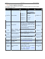
3. Notational convention
The format of registers is described using a diagram of the following form:
31–20
19–17
16–8
7–0
LED[4:2]
W,000000000000
W,100
W,000000000
W,10000000
Figure 1: Register Format
The digits at the top of the diagram indicate bit positions within the register and the
central section names bits or bit fields. The bottom row describes what may be done
to the field and its value after reset. Shaded fields are reserved and should only ever
be written with zeroes.
R
Readable by the CPU
W
Writeable by the CPU
RW
Readable and writeable by the CPU
Binary digits indicate the value of the field after reset
Figure 2: Notational convention
Version 6.1
Page 7 of 24
SMT317 User Manual
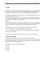
4. Outline Description
The SMT317v2 module is an ADC-based size 1 TIM offering the following features:
•
Eight 16-bits ADCs running at an output word rate of up to 1.2 MHz for input
bandwidths up to 460 kHz.
•
a Xilinx XCV300 Virtex FPGA.
•
FPGA programming via communication port (comm-port3).
•
High bandwidth data I/O via 1 Sundance Digital Bus (SDB).
JUMPERS
ADC SUB-SYSTEM
SYNC
4 LEDs
4 I/Os
Clock
Control Comm-port
selection
8 ADCs
Clock Buffer
Sample clock
VIRTEX
Local clock
37.6 MHz
1 SDB
Clock select
External clock
Internal sync
Comm-port 3
External SYNC
Comm-port 3
CONFIG CPLD
on Comm-port3
PRIMARY
Figure 3: Block Diagram
S
D
B
Version 6.1
Page 8 of 24
SMT317 User Manual
5. Power up sequence
At power up the config CPLD waits for a bitstream to configure the FPGA.
The Virtex FPGA from Xilinx is volatile in nature, and requires reconfiguring every
time the module is powered on.
From the moment the module is powered on to the time when the FPGA is
configured:
•
The ADC sampling clock is the external clock (beware to respect the
maximum frequency rating, see ADC Datasheet AD7723)
•
The ADC SYNC (See ADC Datasheet AD7723) signal is maintained high to
keep the ADCs in reset state
After the FPGA is configured the ADC controls default to the values in
Table 1: Control Register description.
6. ADC Sub-System
It consists of 8 Analog Devices AD7723 converters. These provide an overall system
performance with an ENOB of 14 (minimum) for each of the eight channels.
All ADCs simultaneously sample using the same clock.
6.1. Input Level
The input to the ADC module is DC coupled with a pk-pk level of 4v. This is centred
about 0v.
Vmin= -2v, Vmax= +2v.
6.2.
Output Codes
The converted samples are presented on the SDB connector as 16 bits twos
complement binary.
Code 0x8000 is equivalent to –Vmax
Code 0x0000 is equivalent to 0V
Code 0x7FFF is equivalent to +Vmax
Version 6.1
Page 9 of 24
SMT317 User Manual
7. Communication ports
7.1.
Overview
The SMT317 communication port is an 8-bit, data-parallel, link that follows Texas
Instruments’ TMS320C4x Communication Port standard. Additional information on
the standard is available in the TMS320C4x User’s Guide chapter 12:
Communication ports and the Texas Instrument Module Specification.
The standard gives a TIM six links numbered from 0 to 5. Each link can be a
transmitter or a receiver, and will switch automatically between these states
depending on the way you use it. Writing to a receiver or reading from a
transmitter will cause a hardware negotiation (token exchange) that will reverse
the state of both ends of the link.
Following a processor reset, the first three links (0, 1, and 2) initialise as transmitters
and the remainder (3, 4, and 5) initialise as receivers. When you wire TIMs together
you must make sure that you only ever connect links initialising as transmitters to
links initialising as receivers; never connect two transmitters or two receivers. For
example, connecting link 0 of one TIM to link 4 of another is safe; connecting link 0 of
one TIM to link 2 of another could damage the hardware.
Always connect comm-ports 0, 1, or 2 to comm-ports 3, 4, or 5.
On the SMT320-SMT310Q carrier board the physical connection between
comm-ports is made with FMS cables. You must be careful when connecting
the cables and make sure that one end is inserted in the opposite sense to the
other. One end must have the blue backing facing out and the other must have
the silver backing facing out.
The SMT320 SMT310Q motherboard communicates with the host PC using commport 3 of the site 1 TIM. You should not make any other connections to this commport.
On the SMT317
•
Comm-port 3 is used for the FPGA configuration. It is the only way to
configure the FPGA.
•
Comm-port 3 is used for both configuring the FPGA and afterwards for
controlling the ADCs data acquisition. In that configuration you save one
connection in your system.
•
Nevertheless, if your application requires using a different Comm-port to
control the acquisition, (the FPGA configuration can only be done via
Comm-port3) please contact Sundance as a custom version of the firmware
with more Comm-port connections could be developed for you.
•
The control comm-port selection is achieved by setting
•
JMP1: Control Comm-port Select. The standard version of the firmware only
provides Comm-port 3.
Version 6.1
Page 10 of 24
SMT317 User Manual
8. SDB
The SMT317 provides one Sundance Digital Bus (SDB). This 16-bit data parallel link
for synchronous transmission can achieve high-speed data transfer across 40-way
flat ribbon cables with ground-interlaced 3.3v signals (Ref. SMT3xx-SDB-CAB).
The SDB is connected directly to the Virtex device. The SDB implementation on this
module operates as an output only.
The user defined pins (UD0, UD1) are not used. The write enable pin (WEN) is driven
active (low) by the SMT317 when it is transmitting data on the SDB. The SDB drives
at LVTTL levels. The SDB pinout is described in
Table 4.
The SDB interface present in the SMT317 implements a flow control meaning that
when the receiver on the other end stops receiving, the data is not overwritten but
pills up in the SMT317’s own FIFO until it is full. Only then data is overwritten.
The SDB interface provides a 511 position FIFO. Each position is 32-bit wide.
The 16-bit SDB interface only transfers multiples of 32-bit words.
Only one transfer speed is available on the SMT317 SDB released after 01/09/2005.
The clock speed is 50 MHz.
You should refer to SDB specifications V2.0 and above for technical information.
9. Data formatting
The sampled data is output on the SDB (Sundance Digital Bus) connector.
The physical link presents ADC samples one at a time (16-bit wide) but the SMT317
packets ADC data samples by pairs and sends multiples of 2 x 16-bit packets with
the least significant bit being sent on D0.
The channels are paired in the following manner:
Ch0, Ch4,
Ch1, Ch5,
Ch2, Ch6,
Ch3, Ch7.
Version 6.1
Page 11 of 24
SMT317 User Manual
Enabling a pair of channels is done by setting any one or both of the two control bits
corresponding to the 2 channels from that pair in the control register described
further down.
Only the data corresponding to the enabled channel pairs will be output on the SDB.
On the start of a new acquisition (in continuous or burst mode) the data from the
channel pair selected with the smallest channel number is always output first.
For example, Ch0-Ch4 data is always output before Ch2-Ch6 data. Then samples
are output by increasing channel pair number for the selected channel pairs.
10. Clock selection
10.1. ADCs Sampling clock
All ADCs are sampled at the same time.
The clock source can either be the onboard oscillator or an external clock.
Therefore, the sampling frequency is either given by the clock divider setting for the
onboard clock or by the external clock (the external clock is not affected by the clock
divider setting).
10.2. SDB output clock
For firmware versions released before 01/09/2005, the SMT317 module allows for
the SDB word rate to be set to either 50 or 100MHz as set by JMP2: SDB Clock
speed select.
A lower word rate may be needed when the receiving device is not able to sustain
the faster transfer speed.
In firmware versions released after 01/09/2005, the SDB clock is no more selectable
and the samples are output at a default 50Mhz clock frequency, which can easily
sustain the data rate required by the ADC data.
If the SDB data transmission is not suspended by the ACK signal and that there are
samples buffered in the SMT317 FIFO, the samples are output at the SDB output
clock frequency.
Version 6.1
Page 12 of 24
SMT317 User Manual
10.3. Overflowed FIFOs
In the case the receiving device has a FIFO, which is becoming full, the ACK signal
on the SDB connector can be used to suspend SDB data transmission, whichever
mode is selected (continuous mode or burst mode). As soon as the ACK signal is
released the transmission continues.
Indeed when a data is written in a 511x16-bit FIFO this data is immediately read and
sent via the SDB to the DSP.
But if the ACK signal on the SDB is active the sampled data are stored in the
511x16-bit FIFO. The data are outputted on the SDB cable as soon as the ACK
signal is not active anymore.
If the 511x16-bit FIFO becomes full when the ACK signal is still active the LED1 is lit.
In order to clear the overrun the user has to clear the SDB receiver’s FIFO and send
a new control word to the SMT317.
11. FPGA
A Field Programmable Gate Array (FPGA) is used to manage the ADC data
acquisition, implement one communication ports and one Sundance Digital Bus.
11.1. Fpga configuration
The Virtex FPGA from Xilinx is volatile in nature, and requires reconfiguring every
time the module is powered on. The configuration data (bitstream) must be presented
through Comm-port 3.
The bitstream is supplied on the distribution disk as ‘fpga_smt317v2.bit’.
Please refer to the SMT6500 help file in the section FPGA type TIM configuration for
more information.
When the module is not configured, LED5 will be illuminated. Upon successful
configuration, LED5 will extinguish. (LED5 located near TIM connector.)
12. ADCs Clock Source
The sample rate of the ADCs is derived from one of two sources: either from an
external clock input or via the on-board reference.
The on-board reference clock is generated by a 37.6 MHz oscillator. The highest
ADC clock frequency generated by the on-board clock is 18.8 MHz, which can be
divided up to 16 times. See
Table 1: Control Register description
The maximum external ADC clock frequency is 19.2MHz. This should be TTL
compatible.
It is not possible to divide the external clock using the Programmable Clock Divider.
Version 6.1
Page 13 of 24
SMT317 User Manual
The buffered external clock is used directly as the ADCs sample clock.
13. ADC Control
All of the ADCs are controlled via the comm-port 3. The comm-port 3 must be
selected using the jumper bank
JMP1: Control Comm-port Select.
27
26
25
24
23
22
21
20
Count_data_fifo
Internal trigger
Active trigger level
Continuous mode
Half pwr
Internal Sync
Mode 1
Mode 0
EXT Clock
LED [4:2]
W,000
W,0
W,0
W,0
W,0
W,0
W,0
W,0
W,0
W,0
W,000
15
30
14
29
13
12
11
10
9
8
CH7 CH3 CH6 CH2 CH5 CH1 CH4 CH0
W,0
W,0
W,0
W,0
W,0
W,0
W,0
W,0
7
Rst SDB
31
W,0
Figure 4: ADCs control register
6
5
Not Used
19
4
18
3
17
2
16
Extra Count_data_fifo
bit
28
Trigger_int
The ADC control is provided by configuring a single control register. It allows control
for the clock divider, the clock selection, the trigger source, the mode (), the ADC
enable and the state of three LEDs. This register is described here,
1
CLK DIV
W,0000
0
Version 6.1
Page 14 of 24
SMT317 User Manual
13.1. Programmable Clock Divider
A 4-bit divider is provided which allows generating up to 16 different clock
frequencies for the ADC clock from the on-board reference clock.
ADC Clock Frequency = 18.8 / (Divider Value +1) (MHz)
Sampling frequency = ADC Clock/16
The programmable divider on default setting is to divide by 16.
The programmable divider has no effect on an external clock.
13.2. LED 1
The LED 1 is lit when the 511x16-bit FIFO is full.
In order to clear the overrun the user has to clear the SDB receiver’s FIFO and send
a new control word to the SMT317.
13.3. Synchronization signal
It’s a pulse active high.
If the internal synchronization signal is selected (bit23=1) as soon as a control word
is received a pulse is generated internally to synchronize all the ADCs.
If the external synchronization signal is selected (bit23=0) the user has to send a
pulse active high to the SMT317 via the SYNC connector to make sure all the ADCs
are synchronized together.
13.4. Trigger
In Continuous mode:
The trigger is a level. As long as the trigger is active the data are sent to the
DSP board via the SDB.
The active level is selectable. The trigger can be active high (bit26=1) or active
low (bit26=0).
In Burst mode:
The trigger is an edge.
In the case of an internal trigger, every time a new control word is sent with
burst mode selected and internal trigger selected then a new burst mode
occurs.
In the case of an external trigger, the burst mode occurs as soon as an edge
is detected on JP2 of JMP2 (0). The trigger is edge selectable:
Bit26=1 the burst is triggered on a rising edge.
Bit26=0 the burst is triggered on a falling edge.
Version 6.1
Page 15 of 24
SMT317 User Manual
13.5. Control register description
The following table describes how behave the different fields of the control register
depending on their value.
FIELD
DESCRIPTION
ACTION
DEFAULT
ADC
Clock Frequency
CLK DIV
Rst_SDB
Clock divider.
Reset FIFO
CLKDIV = 0
18.8 Mhz
CLKDIV = 1
9.4 Mhz
CLKDIV = 2
6.27 Mhz
CLKDIV = 3
4.7 Mhz
CLKDIV = 15
1.17 Mhz
CLKDIV=15
Rst_SDB = 1: Clear outgoing SDB
FIFO and send a Reset SDB for
the receiving end (Reset only valid
for SMT332/372).
Rst_SDB = 0
Can be used to synchronise data
at the receiving end
CHx
ADC Channel x CHx = 1 enables ADC channel x
enable in outgoing
CHx = 0 disables ADC channel x
SDB FIFO.
LEDx
LEDx illumination.
CHx = 1
LEDx = 0 lights LEDx
LED[4:2]=101
LEDx = 1 turns LEDx off
EXT Clock
MODE 0,
MODE 1
Select the sampling EXT = 1 selects external clock
Clock source.
EXT = 0 selects internal clock
Parallel/Serial
interface
See ADC Datasheet AD7723
EXT = 0
MODE 0 = 0
MODE 1 = 0
Internal_SYNC = 1, an internal
pulse is sent to SYNC.
Internal
SYNC
Synchronisation
logic
Internal_SYNC = 0, an external Internal_SYNC
signal is used for SYNC.
=0
See ADC Datasheet
about SYNC function.
AD7723
Version 6.1
Half pwr
Continuous
mode
Active level
trigger
Internal
trigger
Trigger_int
Count_data
_fifo
Page 16 of 24
Half Power
Continuous mode
SMT317 User Manual
See ADC Datasheet AD7723
Half_pwr = 0
Continuous mode = 1 selects the
continuous mode
Continuous_
Continuous mode = 0 selects the
burst mode
Active level trigger
mode = 0
Active_level_trigger = 1, trigger
active high or rising edge
Active_level_
Active_level_trigger = 0, trigger Trigger = 0
active low or falling edge
Trigger logic
Trigger signal
Internal_trigger = 1 selects the
internal trigger
Internal_
Internal_trigger = 0 selects the
external trigger
Trigger = 0
To drive the internal trigger in
continuous mode only (enable
signal)
Trigger_int
Countdata_fifo=0000
256 samples
Countdata_fifo=0001
512 samples
CountNumber of data to data_fifo=0010
be
transferred Countduring
a
burst data_fifo=0011
operation.
CountOnly used in burst data_fifo=0100
mode.
CountBit16Bit31Bit30Bit29
data_fifo=0101
Countdata_fifo=0110
=1
1Ksample
2Ksamples
Count_data_
4Ksamples
8Ksamples
16Ksamples
Etc…
up
to
Count_data_fifo= 8Msamples
1111
Table 1: Control Register description
fifo[3:0] = 0000
Version 6.1
Page 17 of 24
SMT317 User Manual
Remark:
The trigger signal is different depending of the mode selected:
•
In burst mode, the trigger is an edge.
•
In continuous mode, the trigger is a level.
The user has to make sure he inputs the right external trigger signal according to the
mode selected.
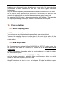
14. Connectors and Jumpers Positions
JMP1
Figure 5: SMT317v2 top view
JMP2
Version 6.1
Page 18 of 24
SMT317 User Manual
15. Connectors
SYN connector (bottom right end side of the top view) is for synchronising all ADCs
operated from a common master clock. It allows each ADC to simultaneously sample
its analog input and update its output register (See ADC Datasheet AD7723).
CLOCK connector (bottom right end side of the top view) is for the external clock.
CH X are the analog inputs.
WARNING!!!
The connector of the channel 7 is very close to the 3.3V. However the ADC female
connector is connected to the ground. It’s very important to check that the ADC
female connector and the 3.3V are not in contact to avoid any short cut, which could
damage the system. The best is to have a straight ADC female connector instead of
a right-angled connector for this channel.
Version 6.1
Page 19 of 24
SMT317 User Manual
16. Jumpers
JMP1 is a header located to the left of the JTAG pins,
JMP2 is a header to the right, closer to the TIM connector.
The Jumpers JPx are numbered from the left to the right: JP1, JP2, JP3 for each
connector JMPx
JP1, JP2 and JP3 refer to the following link positions on JMPx:
JP1 JP2 JP3
Figure 6: JUMPER JMPx
16.1. JMP1: Control Comm-port Select
JP1
JP2
JP3
Comm Port
OUT
OUT
OUT
N/A
OUT
OUT
IN
N/A
OUT
IN
OUT
N/A
OUT
IN
IN
3
IN
OUT
OUT
N/A
IN
OUT
IN
N/A
Table 2: Comm-port selection
Version 6.1
Page 20 of 24
SMT317 User Manual
16.2. JMP2: SDB Clock speed select and external trigger
•
SDB Clock speed select:
JP1
JP2
JP3
CLK (MHz)
IN
N/A
N/A
50
OUT
N/A
N/A
100
Table 3: Clock speed selection
•
External trigger
JP2 is used to apply the external trigger signal.
The trigger signal is different depending of the mode selected:
•
In burst mode, the trigger is an edge.
•
In continuous mode, the trigger is a level.
The user has to make sure he inputs the right external trigger signal according
to the mode selected.
Version 6.1
Page 21 of 24
SMT317 User Manual
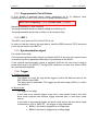
17. Input Circuitry
The jumper located near the channel input connector is used to select the input
mode.
If the jumper is installed it selects single-ended input.
C10
1uF
C11
100nF
REF1
ADC
R11
1
0AV
R12
+
R4
C1
2
510K
J1
U1A
R2 510K
8
3
CH0+
CH0-
1
2
3
4
5
470nF
2
4
R9
OPA2350
8
IN+
1
OUT
IN4
R1 27R
10K
R3 10K
C7
220pF
R8
510K
U1B
R6 510K
5
6
J2
2
1
R10
10K
8
IN+
R5 27R
OUT
7
IN4
OPA2350
JMP2
R7 10K
Figure 7: ADC Input circuitry
VIN (+)
ADC
VIN (-)
ADC
Version 6.1
Page 22 of 24
SMT317 User Manual
17.1. SDB Pinout
Function
Pin
Pin
Function
GND
2
1
CLK
GND
4
3
DATA0
GND
6
5
DATA1
GND
8
7
DATA2
GND
10
9
DATA3
GND
12
11
DATA4
GND
14
13
DATA5
GND
16
15
DATA6
GND
18
17
DATA7
GND
20
19
DATA8
GND
22
21
DATA9
GND
24
23
DATA10
GND
26
25
DATA11
GND
28
27
DATA12
GND
30
29
DATA13
GND
32
31
DATA14
GND
34
33
DATA15
GND/DIR
36
35
USERDEF0
REQ
38
37
WEN
ACK
40
39
USERDEF1
Table 4: SDB Pinout.
Version 6.1
Page 23 of 24
SMT317 User Manual
18. Example Code
Code to use with a smt335.
Comm-port 1 (SMT335) have to be connected to the Comm-port 3 (SMT317).
The SDB (SMT317) is linked with the SDB B (SMT335).
#include <stdio.h>
#include <sema.h>
#include <thread.h>
#include "smt317v2.h"
#include "Fast_FpgaConf.c"
#include "sdb.h"
/********************** PROTOTYPES ***********************/
void fill_internal_b(void *);
void Fast_FpgaConf(int len, unsigned int *b, int link_no);
void *calloc(size_t _num, size_t _size);
/*********************************************************/
#define BURST1K_IntClk_IntTrigger_low_IntSync 0X49ea0101
SEMA internal_filled_b;
int *samplestore;
main()
{
//Corresponds to the only bitstream in the Dat2asm.bat file
extern far int fpga_count;
extern far unsigned int fpga_data[];
int control_word;
Version 6.1
Page 24 of 24
SMT317 User Manual
//Allocation of a memory space to store the samples
samplestore=(int*)calloc(BUFFER_SIZE,sizeof(int));
if (samplestore!=NULL & samplestore_slave!=NULL)
printf("memory allocation was successful\n");
else
exit(1);
printf("Address of samplestore:%08x \n",samplestore);
/******************FPGA CONFIGURATION*********************/
printf("\nFirst bitstream\n");
Fast_FpgaConf(fpga_count, fpga_data, COMMPORT1);
printf("\nEND... \n");
/*******************ACQUISITION***************************/
SDB_init(SDB_CLROF|SDB_CLRIF|SDB_CLK,
SDB_CLROF|SDB_CLRIF|SDB_CLK);
control_word = BURST1K_IntClk_IntTrigger;
link_out_word(control_word, COMMPORT1);
sema_init(&internal_filled_b, 0);
thread_new(fill_internal_b, 1000, 0);
sema_wait(&internal_filled_b);
printf("done\n");
}
void fill_internal_b(void *x)
{
SDB_read (BUFFER_SIZE*sizeof(int), samplestore, SDB_B);
sema_signal(&internal_filled_b);
}