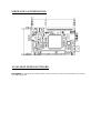
1
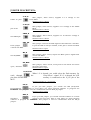
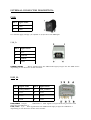
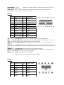
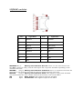
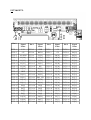
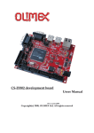
LPC-E2468 development board
Users Manual
Rev.B, February 2008
Copyright(c) 2008, OLIMEX Ltd, All rights reserved
INTRODUCTION:
LPC-E2468 uC Linux development prototype board with LPC2468 USB,
Ethernet, SD/MMC in credit card format.
BOARD FEATURES:
-
MCU: LPC2468;
-
16MB SDRAM;
-
128 MB NAN Flash;
-
standard JTAG connector with ARM
programming/debugging with ARM-JTAG;
-
Ethernet 100MBit;
-
2x USB hosts;
-
USB-to-RS232 converter device connected to LPC2468 UART;
-
SD/MMC card connector;
-
UEXT connector with I2C, SPI, RS232 and power supply for
connecting add-on modules like RF link, MP3, etc available from
Olimex;
-
trimpot connected to ADC;
-
RESET circuit with external control of Philips ISP utility via RS232
port;
-
two USER button;
-
RESET Button;
-
two on board voltage regulators 3V and 5V with up to 800mA
current;
-
Extension port connector for many of microcontrollers pins;
-
single power supply: External power supply, USB or JTAG connector;
-
Battery holder and connector for the RTC;
-
power supply led;
-
FR-4, 1.5 mm, red soldermask, component print;
-
Dimensions: 90x60mm (3.54 x 2.36").
2x10
pin
layout
for
ELECTROSTATIC WARNING:
The LPC-E2468 development board is shipped in protective anti-static
packaging. The board must not be subject to high electrostatic potentials.
General practice for working with static sensitive devices should be applied
when working with this board.
BOARD USE REQUIREMENTS:
Cables:
USB A-B cable to connect to virtual serial port on the board.
You will need LPT cable if you want to program the MCU with
AVR-JTAG. You might need other cables in case of other
programmers/debuggers.
Hardware:
Software:
Programmer/debugger AVR-JTAG or any compatible tool.
The board is delivered with uC Linux pre-loaded. You could
develop projects for the board with Eclipse, IAR, etc. Please,
refer to the LPC-E2468 Quickstart Guide which is on the CD
for more details on the software requirements.
PROCESSOR FEATURES:
The LPC2468 processor has the following features:
●
ARM7TDMI-S processor, running at up to 72 MHz.
●
512 kB on-chip flash program memory with In-System Programming
(ISP) and In-Application Programming (IAP) capabilities. Flash
program memory is on the ARM local bus for high performance CPU
access.
●
98 kB on-chip SRAM includes:
▬
64 kB of SRAM on the ARM local bus for high performance CPU
access.
▬
16 kB SRAM for Ethernet interface. Can also be used as
general purpose SRAM.
▬
16 kB SRAM for general purpose DMA use also accessible by
the USB.
▬
2 kB SRAM data storage powered from the Real-Time Clock
(RTC) power domain.
●
Dual Advanced High-performance Bus (AHB) system allows
simultaneous Ethernet DMA, USB DMA, and program execution
from on-chip flash with no contention.
●
EMC provides support for asynchronous static memory devices such
as RAM, ROM and flash, as well as dynamic memories such as
Single Data Rate SDRAM.
●
Advanced Vectored Interrupt Controller (VIC), supporting up to 32
vectored interrupts.
●
General Purpose AHB DMA controller (GPDMA) that can be used
with the SSP,
●
I2S-bus, and SD/MMC interface as well as for memory-to-memory
transfers.
●
Serial Interfaces:
▬
Ethernet MAC with MII/RMII interface and associated DMA
controller. These functions reside on an independent AHB bus.
▬
USB 2.0 full-speed dual port Device/Host/OTG Controller with
on-chip PHY and associated DMA controller.
●
▬
Four UARTs with fractional baud rate generation, one with
modem control I/O, one with IrDA support, all with FIFO.
▬
CAN controller with two channels.
▬
SPI controller.
▬
Two SSP controllers, with FIFO and multi-protocol capabilities.
One is an alternate for the SPI port, sharing its interrupt. SSPs
can be used with the GPDMA controller.
▬
Three I2C-bus interfaces (one with open-drain and two with
standard port pins).
▬
I2S (Inter-IC Sound) interface for digital audio input or output.
It can be used with the GPDMA.
Other peripherals:
▬
SD/MMC memory card interface.
▬
160 General purpose I/O pins with configurable pull-up/down
resistors.
▬
10-bit ADC with input multiplexing among 8 pins.
▬
10-bit DAC.
▬
Four general purpose timers/counters with 8 capture inputs
and 10 compare outputs. Each timer block has an external
count input.
▬
Two PWM/timer blocks with support for three-phase motor
control. Each PWM has an external count inputs.
▬
RTC with separate power domain, clock source can be the RTC
oscillator or the APB clock.
▬
2 kB SRAM powered from the RTC power pin, allowing data to
be stored when the rest of the chip is powered off.
▬
WatchDog Timer (WDT). The WDT can be clocked from the
internal RC oscillator, the RTC oscillator, or the APB clock.
●
Standard ARM test/debug interface for compatibility with existing
tools.
●
Emulation trace module supports real-time trace.
●
Single 3.3 V power supply (3.0 V to 3.6 V).
●
Three reduced power modes: idle, sleep, and power-down.
●
Four external interrupt inputs configurable as edge/level sensitive.
All pins on PORT0 and PORT2 can be used as edge sensitive
interrupt sources.
●
Processor wake-up from Power-down mode via any interrupt able to
operate during Power-down mode (includes external interrupts, RTC
interrupt, USB activity, Ethernet wake-up interrupt, CAN bus
activity, PORT0/2 pin interrupt).
●
Two independent power domains allow fine tuning of power
consumption based on needed features.
●
Each peripheral has its own clock divider for further power saving.
These dividers help reducing active power by 20 - 30 %.
●
Brownout detect with separate thresholds for interrupt and forced
reset.
●
On-chip power-on reset.
On-chip crystal oscillator with an operating range of 1 MHz to 24 MHz.
●
4 MHz internal RC oscillator trimmed to 1 % accuracy that can
optionally be used as the system clock. When used as the CPU clock,
does not allow CAN and USB to run.
●
On-chip PLL allows CPU operation up to the maximum CPU rate
without the need for a high frequency crystal. May be run from the
main oscillator, the internal RC oscillator, or the RTC oscillator.
●
Boundary scan for simplified board testing.
●
Versatile pin function selections allow more possibilities for using
on-chip peripheral functions.
BLOCK DIAGRAM:
MEMORY MAP:
LPC2468 memory map
SCHEMATIC:
BOARD LAYOUT:
POWER SUPPLY CIRCUIT:
LPC-E2468 can take power from power connector PWR, where +(9-12) VDC
or (6-9) VAC external voltage source has to be applied. The board could also
take power from USB_D or from battery. Note: the battery only supplies the
internal 2MB SRAM and the RTC.
The board power consumption is: about 150 mA at 9VDC.
RESET CIRCUIT:
LPC-E2468 reset circuit is made with RC group R4 – 47K, C20 – 100nF
and RESET button.
CLOCK CIRCUIT:
Quartz crystal 12MHz is connected to LPC2468 pin 44 (XTAL1) and pin 46
(XTAL2).
32.768 KHz quartz crystal is connected to LPC2468 pin 34 (RTCX1) and
pin 36 (RTCX2) for its internal Real Time Clock.
JUMPER DESCRIPTION:
3.3V_E
This jumper, when closed, supplies 3.3 V voltage to the
of the MCU.
Default state is closed.
VDD1-10 pins
3.3VA_E
This jumper, when closed, supplies 3.3 V voltage to the VDDA
MCU.
Default state is closed.
pin of the
VREF_E
This jumper, when closed, supplies 3.3 V reference voltage to
of the MCU.
Default state is closed.
the VREF pin
PHY_PD
This jumper controls the PHY signal of the Ethernet controller.
is pen the PHY is always enabled, if the pin is closed the MCU
If the jumper
controls the PHY.
Default state is open.
WP_E
This jumper, when closed, inputs the Write protect signal from
card to the MCU.
Default state is closed.
the SD/MMC
NF_WPE
This jumper, when closed, write-protects the flash and when
the write protection.
Default state is open.
open, disables
N_CE/CS1
work through
pin of the NAND flash
MCU.
When 1-2 is shorted, you could select the flash memory for
the
Chip Select 1 signal. If 2-3 is shorted, the #CE
memory is connected to the N_CE pin of the
Default position is 1-2 shorted.
ISP_E
If you put this jumper, you enable the ISP (In-System
Programming).
This is used when you want external software to program the
LCP2478. This jumper is used in combination with the RST_E jumper.
Default state is open.
RST_E
If you put this jumper, you enable external software to control
the Reset
signal to the processor. This is used when you want external
software to program the LCP2478. This jumper is used in combination with the ISP_E
jumper.
Default state is open.
BDS_E
Boundary scan enable.
Default state is open.
BAT/EXT
pin.
This jumper controls the input power supply for the VBAT
the
If 1-2 are shorted, the external battery is connected to
VBAT pin.
on-
If 2-3 are shorted, the VBAT pin is supplied by the
board +3.3V supply.
Default state is 2-3 shorted.
EXT/USB_D
the
+3.3V
This jumper controls 3.3V power supply for the board.
If 1-2 are shorted, the external power (from the PWR
jack and after the +5V voltage regulator) is input to
+3.3V voltage regulator and supplies the board.
If 2-3 are shorted, the USB device provides +5V to the
voltage regulator and supplies the board.
Default state is 1-2 shorted.
INPUT/OUTPUT:
One reset button with name RESET – connected to LPC2468 pin 35
(#RESET).
Two user buttons with names BUT1 – connected to LPC2468 pin 102
(P2[13]/#EINT3/MCIDAT3/I2STX_SDA) and BUT2 – connected to LPC2468
pin 81 (P2[21]/#DYCS1);
Two LEDs named STAT1(green) and STAT2(red) – connected to LPC2468
pin 104 (P4[17]/A17) and LPC2468 pin101 (P4[16]/A16);
Two yellow LEDs named USB_1 and USB_2 – connected to LPC2468 pin 66
(P1[18]/USB_UP_LED1/PWM1[1]/CAP1[0])
and
LPC2468
pin
45
(P0[13]/USB_UP_LED2/MOSI1/AD0[7]);
One red LED named SD indicating that SD/MMC card is powered up;
Power supply red LED with name PWR – indicates that 3.3V is present.
EXTERNAL CONNECTOR DESCRIPTION:
PWR:
Pin # Signal Name
1
PWR
2
GND
You should apply voltage +(9-12)VDC or (6-9) VAC at the PWR pin.
USB_D:
Pin # Signal Name
1
VCC
2
USBDM
3
USBDP
4
GND
USBDM, USBDP
These signals form the differential input/output for the USB device
depending on the direction of the data flow.
USB_H:
Pin # Signal Name
Pin # Signal Name
1
USB_PWRD1
5
USB_PWRD2
2
U1D-
6
U2D-
3
U1D+
7
U2D+
4
GND
8
GND
USB_PWRD1 Output
USB Power 1. This signal is output from the processor and
input for the USB host 1.
U1D-, U1D+ I/O
This signals form the differential input/output for USB host 1
depending on the direction of the data transfer.
USB_PWRD2 Output
USB Power 2. This signal is output from the processor and
input for the USB host 2.
U2D-, U2D+ I/O
This signals form the differential input/output for USB host 2
depending on the direction of the data transfer.
JTAG:
Pin # Signal Name
Pin #
Signal Name
1
3.3V
2
3.3V
3
TRSTN
4
GND
5
TDI
6
GND
7
TMS
8
GND
9
TCK
10
GND
11
RTCK
12
GND
13
TDO
14
GND
15
RSTN
16
GND
17
10K to GND
18
GND
19
10K to GND
20
GND
TDI
Input Test Data In. This is the serial data input for the shift register.
TDO OutputTest Data Out. This is the serial data output for the shift register. Data is
shifted out of the device on the negative edge of the TCK signal.
TMS Input Test Mode Select. The TMS pin selects the next state in the TAP state
machine.
TCK Input Test Clock. This allows shifting of the data in, on the TMS and TDI pins. It is
a positive edge triggered clock with the TMS and TCK signals that define the internal state of
the device.
TRSTNInput Test Reset N. This signal resets the JTAG controller.
RTCK OutputReturn Clock. This is a synchronization signal which the JTAG connector
uses to acknowledge it is ready to receive/transmit.
RSTN Input Reset. This signal resets the MSU.
JTAG is used to to program and debug the MCU.
UEXT:
Pin #
Signal Name
Pin # Signal Name
1
3.3V
2
GND
3
TXD1
4
RXD1
5
SCL0
6
SDA0
7
MISO
8
MOSI
9
SCK
10
SSEL
TXD1 OutputTransmit Data. This is the asynchronous serial data output (RS232) for the
RS232 interface.
RXD1 Input Receive Data. This is the asynchronous serial data input (RS232) for the
RS232 interface.
SCL0
I/O
Serial (Synchronization) Clock. This is the synchronization clock for
the data transfer through I2C interface. This could be either input or output depending on
whether the MCU is master or slave.
SDA0
I/O
Serial Data. This pin is data input or output (depending on the data
flow direction) for the I2C interface.
MISO
I/O
Master In Slave Out. This pin could be either data input (MCU is
master) or data output(MCU is slave). The signal is pat of the SPI interface.
MOSI
I/O
Master Out Slave In. This pin is be used for communication through
SPI interface and it is either data output from the MCU (when it is master) or data input for
the MCU (when it is slave).
SCK
I/O
Serial (Synchronization) Clock . This is the synchronization clock
for the data transfer through the SPI interface. It could be either input or output depending
on whether the MCU is master or slave.
SSEL
I/O
Slave Select. This is the slave select signal for the SPI interface. If the
MCU is master, this is output. If the MCU is slave, this signal is input.
LAN:
Pin #
Signal Name Chip Side
Signal Name Chip Side
1
TD+
5
Not Connected (NC)
2
TD-
6
Not Connected (NC)
3
3.3V
7
RD+
4
Not Connected (NC)
8
RD-
LED
TDTD+
RDRD+
Pin #
Color
Usage
Right
Yellow
Activity
Left
Green
100MBits/s (Half/Full duplex)
OutputDifferential
OutputDifferential
Input Differential
Input Differential
signal
signal
signal
signal
output. This signal is output from the MCU.
output. This signal is output from the MCU.
input. This signal is input for the MCU.
input. This signal is input for the MCU.
SD/MMC card slot:
Pin #
Signal Name
Pin #
Signal Name
1
MCIDAT3
2
MCICMD
3
GND (VSS1)
4
VDD
5
MCICLK
6
GND (VSS2)
7
MCIDAT0
8
MCIDAT1
9
MCIDAT2
10
WP
11
-
12
-
13
CP
14
GND
15
GND
MCIDAT0-3 I/O
Memory Card Interface Data 0-4. These are the data lines for the
SD/MMC connector. They could be both input and output for the MCU depending on the
data flow direction.
MCICMD
Output Memory Card Interface Command. This is a command sent form the
processor to the memory card and as such it is output from the processor.
MCICLK
Output Memory Card Interface Clock. This signal is output from the MCU
and synchronizes the data transfer between the memory card and the MCU.
WP
Input Write Protect. This signal is input for the MCU.
CP
Input Card Present. This signal is input for the MCU.
EXT1&EXT2:
Pin #
Signal
Name
Pin #
Signal
Name
Pin #
Signal
Name
Pin #
Signal
Name
EXT1-1
3.3V
EXT1-2
GND
EXT2-1
3.3V
EXT2-2
GND
EXT1-3
+5V
EXT1-4
RSTN
EXT2-3
+5V
EXT2-4
P4[23]
EXT1-5
ALARM
EXT1-6
P1[29]
EXT2-5
P4[22]
EXT2-6
P4[21]
EXT1-7
P1[28]
EXT1-8
P1[26]
EXT2-7
P4[20]
EXT2-8
P3[31]
EXT1-9
P1[25]
EXT1-10
P1[24]
EXT2-9
P3[30]
EXT2-10
P3[29]
EXT1-11
P1[23]
EXT1-12
P1[21]
EXT2-11
P3[28]
EXT2-12
P3[27]
EXT1-13
P1[20]
EXT1-14
WP
EXT2-13
P3[26]
EXT2-14
P3[25]
EXT1-15
P0[26]
EXT1-16
P0[25]
EXT2-15
P3[24]
EXT2-16
P3[23]
EXT1-17
VREF
EXT1-18
P0[24]
EXT2-17
P3[22]
EXT2-18
P3[21]
EXT1-19
P0[23]
EXT1-20
P0[22]
EXT2-19
P3[20]
EXT2-20
P3[19]
EXT1-21
P0[21]
EXT1-22 PHY_PD EXT2-21
P3[18]
EXT2-22
P3[17]
EXT1-23
P0[19]
EXT1-24
P0[14]
EXT2-23
P3[16]
EXT2-24
P2[31]
EXT1-25
P0[11]
EXT1-26
P0[10]
EXT2-25
P2[30]
EXT2-26
P2[27]
EXT1-27
P0[9]
EXT1-28
P0[8]
EXT2-27
P2[26]
EXT2-28
P2[25]
EXT1-29
P0[7]
EXT1-30
P0[6]
EXT2-29
P2[23]
EXT2-30
P2[22]
EXT1-31
P0[5]
EXT1-32
P0[4]
EXT2-31
P2[15]
EXT2-32
P2[14]
EXT1-33
P0[1]
EXT1-34
P0[0]
EXT2-33
P2[9]
EXT2-34
P2[8]
EXT1-35
P4[30]
EXT1-36
P4[29]
EXT2-35
P2[7]
EXT2-36
P2[6]
EXT1-37
P4[28]
EXT1-38
P4[27]
EXT2-37
P2[5]
EXT2-38
P2[4]
EXT1-39
P3[26]
EXT1-40
P4[15]
EXT2-39
P2[3]
EXT2-40
P2[2]
MECHANICAL DIMENSIONS:
All measures are in mm.
AVAILABLE DEMO SOFTWARE:
LPC-E2468 is delivered pre-loaded with C Linux and the sources and binaries are on the
accompanying CD.
ORDER CODE:
LPC-E2468 – assembled and tested (no kit, no soldering required)
How to order?
You can order to us directly or by any of our distributors.
Check our web www.olimex.com/dev for more info.
All boards produced by Olimex are RoHS compliant
Revision history:
REV.A
- created February 2008
Disclaimer:
© 2008 Olimex Ltd. All rights reserved. Olimex®, logo and combinations thereof, are registered trademarks of
Olimex Ltd. Other terms and product names may be trademarks of others.
The information in this document is provided in connection with Olimex products. No license, express or implied
or otherwise, to any intellectual property right is granted by this document or in connection with the sale of Olimex
products.
Neither the whole nor any part of the information contained in or the product described in this document may be
adapted or reproduced in any material from except with the prior written permission of the copyright holder.
The product described in this document is subject to continuous development and improvements. All particulars of
the product and its use contained in this document are given by OLIMEX in good faith. However all warranties
implied or expressed including but not limited to implied warranties of merchantability or fitness for purpose are
excluded.
This document is intended only to assist the reader in the use of the product. OLIMEX Ltd. shall not be liable for
any loss or damage arising from the use of any information in this document or any error or omission in such
information or any incorrect use of the product.