1
MVME410/D2
MVME410
Dual Parallel Port Module
User's Manual
QUALITY
•
PEOPLE
•
PERFORMANCE
MVME410/D2
AUGUST 1983
MVME410
DUAL PARALLEL PORT MODULE
USER'S MANUAL
The information in this document has been carefully checked and is believed to
entirely reliable. However, no responsibility is assumed for inaccuracies.
Furthermore, Motorola reserves the right to make changes to any products herein
to improve reliability, function, or design.
Motorola does not assume any
liability arising out of the application or use of any product or circuit
described herein; neither does it convey any license under its patent rights or
the rights of others.
~
I/Onodule is a trademark of Motorola Inc.
Secom Frlition
Copyright 1982 by Motorola Inc.
First Frlition October 1982
SAFETY SUMMARY
SAFETY DEPENDS ON YOU
The fol/owing general safety precautions must be observed during all phases of operation, service, and
repair of this equipment. Failure to comply with these precautions or with specific warnings elsewhere
In this manual violates safety standards of design, manufacture, and Intended use of the equipment.
Motorola Inc. assumes no liability for the customer's failure to comply with these requirements. The
safety precautions /Isled below represent warnings of certain dangers of which we are aware. You, as
the user of the product, should follow these warnings and all other safety precautions necessary for
the safe operation of the equipment In your operating environment.
GROUND THE INSTRUMENT.
To minimize shock hazard, the equipment chassis and enclosure must be connected to an electrical
ground. The equipment is supplied with a three-conductor ac power cable. The power cable must either
be plugged into an approved three-contact electrical outlet or used with a three-contact to two-contact
adapter, with the grounding wire (green) firmly connected to an electrical ground (safety ground) at the
power outlet. The power jack and mating plug of the power cable meet International Electrotechnical
Commission (IEC) safety standards.
DO NOT OPERATE IN AN EXPLOSIVE ATMOSPHERE.
Do not operate the equipment in the presence of flammable gases or fumes. Operation of any electrical
equipment in such an environment constitutes a definite safety hazard.
KEEP AWAY FROM LIVE CIRCUITS.
Operating personnel must not remove equipment covers. Component replacement and internal adjustments must be made by qualified maintenance personnel. Do not replace components with power
cable connected. Under certain conditions, dangerous voltages may exist even with the power cable
removed. To avoid injuries, always disconnect power and di~charge circuits before touching them.
DO NOT SERVICE OR ADJUST ALONE.
Do not attempt internal service or adjustment unless another person, capable of rendering first aid and
resuscitation, is present.
USE CAUTION WHEN EXPOSING OR HANDLING THE CRT.
Breakage of the Cathode-Ray Tube (CRT) causes a high-velocity scattering of glass fragments (implosion). To prevent CRT implosion, avoid rough handling or jarring of the equipment. Handling of the
CRT should be done only by qualified maintenance personnel using approved safety mask and gloves.
DO NOT SUBSTITUTE PARTS OR MODIFY EQUIPMENT.
Because of the danger of introducing additional hazards, do not install substitute parts or perform any
unauthorized modification of the equipment. Contact Motorola Microsystems Warranty and Repair for
service and repair to ensure ~hat safety features are maintained.
DANGEROUS PROCEDURE WARNINGS.
Warnings, such as the example below, precede potentially dangerous procedures throughout this
manual. Instructions contained in the warnings must be followed. You should also employ all other
safety precautions which you deem necessary for the operation of the equipment in your operating
environment.
WARNING
Dangerous voltages, capable of causing death, are present In this equipment. Use extreme
caution when handling, testing, and adjusting.
14260 PRINTED IN USA (61811 MPS 300
PREFACE
Unless otherwise specified, all address references are in hexadecimal
throughout this manual.
asterisk (*) following the signal name for signals which are level
significant denotes that the signal is true or valid When the signal
is low.
An
An asterisk (*) following the signal name for signals which are edge
significant denotes that the actions initiated by that signal occur
on a high to low transition.
Throughout this manual, the X in the signal mI'lemonic of peripheral
signals (i.e., PXCBl, PXCB2) denotes the following:
X = 1 denotes Jl front panel connector
X = 2 denotes Jl6 front panel connector
TABLE OF CONTENTS
CHAPTER 1
1.1
1.2
1.3
1.4
1.5
CHAPTER 2
GENERAL INFORMATION
INTRODUCTION •••••••••••••••••••••••••••••••••••••••••••••
FEATURES •••••••••••••••••••••••••••••••••••••••••••••••••
SPECIFICATIONS •••••••••••••••••••••••••• ·• ••••••••••••••••
GENERAL DESCRIPTION ••••••••••••••••••••••••••••••••••••••
REI.ATED DOCUMENTATION ••••••••••••••••••••••••••••••••••••
HARDWARE PREPARATION AND INSTALLATION INSTRUCTIONS
2.1
IN'l'RODUCTI 00 •••••••••••••••••••••••••••••••••••••••••••••
2.2
2.3
2.3.l
2.3.2
2.3.3
2.3.4
2.3.5
2.3.6
2.3.7
2.3.8
2.4
2.4.1
2.4.2
UNPACKIN3 INSTRUCTIONS•••••••••••••••••••••••••••••••••••
HARDWARE PREPARATION' •••••••••••••••••••••••••••••••••••••
LED Monitor Header (J2)
Port 1 Direction Headers (J3, J4) ••••••••••••••••••••••
Port 1 Direction Headers (JS, J6) ••••••••••••••••••••••
Port 2 Direction Headers (J8' J9) ••••••••••••••••••••••
Port 2 Direction Headers (JlO, Jll) ••••••••••••••••••••
Interrupt Select Headers (Jl2, Jl3)
Base Address Selection Header (Jl4)
LED Control Header (Jl5)
INSTALI.ATION INSTRUCTIONS ••••••••••••••••••••••••••••••••
Installation in VME Chassis ••••••••••••••••••••••••••••
Installation in 5-Slot I/Qnodule card Cage •••••••••••••
CHAPTER 3
3.1
3.2
3.3
CHAPTER 4
4.1
4.2
4.3
4.3.1
4.3.2
4.3.3
4.4
4.5
4.6
4.7
4.8
1-1
1-1
1-1
1-5
1-5
....................
2-1
2-1
2-1
2-3
2-4
2-5
2-6
2-7
2-8
2-9
2-11
2-12
2-12
2-12
OPERATIN3 INSTRUCTIONS
IN'l'RODUCTI ON •••••••••••••••••••••••••••••••••••••••••••••
INDICATOR
OPERATI~
................................................
PROCEDURE ••••••••••••••••••••••••••••••••••••••
3-1
3-1
3-1
FUNCTIONAL DESCRIPTION
INTRODUCTION •••••••••••••••••••••••••••••••••••••••••••••
GENERAL DESCRIPTION ••••••••••••••••••••••••••••••••••••••
I/O CHANNEL INTERFACE ••••••••••••••••••••••••••••••••••••
Map Decoding Logic
Access Control Logic
Interrupt Logic ti • • • • • • • • • • • • • • • • • • • • • • • • • • • • • • • • • • • • • • •
PARALLEL PORT 1
PARALLEL PORT 2 ••••••••••••••••••••••••••••••••••••••••••
LIMITATIONS ••••••••••••••••••••••••••••••••••••••••••••••
MODULE I/O TIMIN:;
MODULE PERIPHERAL TIMI~ •••••••••••••••••••••••••••••••••
.....................................
...................................
..........................................
........................................
i
4-1
4-1
4-1
4-1
4-1
4-2
4-5
4-5
4-6
4-6
4-7
TABLE OF CONTENTS (cont'd)
CHAPrER S
S.l
S.2
s.2.1
S.2.2
S.3
S.4
SUPPORT INFORMATION
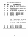
INTRODUCTI,ON •••••••••••••••••••••••••••••••••••••••••••••
CONNECTOR SIGNAL DESCRIPTIONS ••••••••••••••••••••••••••••
I/O Channel Connector ••••••••••••••••••••••••••••••••••
Peripheral Connectors ••••••••••••••••••••••••••••••••••
PARTS LIST •••••••••••••••••••••••••••••••••••••••••••••••
DIAGR.AMS •••••••••••••••••••••••••••••••••••••• • •••• • • • • • •
S-1
S-1
S-1
S-1
S-1
S-1
LIST OF ILLUSTRATIONS
FIGURE 1-1.
2-1.
2-2.
2-3.
2-4.
2-S.
2-6.
2-7.
2-8.
2-9.
2-10.
3-1.
4-1.
4-2.
4-3.
4-4.
5-1.
5-2.
Dual Parallel Port Module ••••••••••••••••••••••••••••••••
OPP Module Header Location Diagram •••••••••••••••••••••••
LED Monitor Header (J2) ••••••••••••••••••••••••••••••••••
Port 1 Direction Headers (J3, J4) ••••••••••••••••••••••••
Port 1 Direction Headers (JS, J6) ••••••••••••••••••••••••
Port 2 Direction Headers (J8, J9) ••••••••••••••••••••••••
Port 2 Direction Headers (JlO, Jll) ••••••••••••••••••••••
Interrupt Select Headers (Jl2, Jl3) ••••••••••••••••••••••
Base Address Select Header (Jl4) •••••••••••••••••••••••••
LED Control Header (JlS) •••••••••••••••••••••••••••••••••
Typical OPP Interface Cabling Diagram ••••••••••••••••••••
Typical Printer Driver Routine (3 Sheets) ••••••••••••••••
OPP Module Block Diagram ···························~·····
I/O Channel Memory Map •••••••••••••••••••••••••••••••••••
I/O Channel Side Timing Signal Diagram •••••••••••••••••••
Peripheral Side Timing Signal Diagram (3 sheets) •••••••••
OPP Module Parts Location Diagram ••••••••••••••••••••••••
DPP Module Schematic Diagram (2 Sheets) ••••••••••••••••••
1-2
2-2
2-3
2-4
2-S
2-6
2-7
2-8
2-10
2-11
2-13
3-2
4-2
4-3
4-7
4-8
S-7
S-9
LIST OF TABLES
TABLE
1-1.
1-2.
2-1.
2-2.
2-3.
2-4.
2-S.
2-6.
2-7.
2-8.
4-1.
4-2.
4-3.
5-1.
S-2.
5-3.
Dual Parallel Port Module Specifications •••••••••••••••••
Peripheral Signal Specifications •••••••••••••••••••••••••
OPP Module Headers •••••••••••••••••••••••••••••••••••••••
Headers J3 am J4 Configurations •••••••••••••••••••••••••
Headers JS and J6 Configurations •••••••••••••••••••••••••
Headers J8 am J9 Configurations •••••••••••••••••••••••••
Headers JlO and Jll Configurations •••••••••••••••••••••••
Headers Jl2 am Jl3 Configurations •••••••••••••••••••••••
Header Jl4 Configurations ••••••••••••••••••••••••••••••••
Header JlS Configurations ••••••••••••••••••••••••••••••••
OPP Module Register Addresses ••••••••••••••••••••••••••••
I/O Channel Timing Signal Characteristics ••••••••••••••••
Peripheral Timing Signal Characteristics •••••••••••••••••
I/O Connector Pl Pin Assignments •••••••••••••••••••••••••
Peripheral Connectors Jl and Jl6 Pin Assignments •••••••••
OPP Module Parts List ••••••••••••••••••••••••••••••••••••
ii
1-3
1-4
2-3
2-4
2-S
2-6
2-7
2-9
2-10
2-11
4-4
4-6
4-7
S-2
S-4
s-s
CHAPTER 1
GENERAL INFORMATION
1.1
INTRODUCTION
'Ibis manual provides general infonnation, hardware preparation and installation
instructions, operating instructions, functional description, and support
information for the MVME410 :rual Parallel I-Ort M:>dule {referred to as DPP
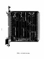
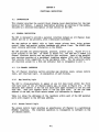
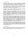
throi..ghout this manual) • 'Ihe OPP is shown in Figure 1-1.
1.2 FEATURES
Features of the OPP are listed below •
• M:>torola I/O Channel compatible •
• Single-wide VME board fonn factor •
• Centronics printer standard interface compatible •
• Two MC6821 Peripheral Interface Adapter {PIA) buffered ports •
• Each port capable of driving two of four I/O Channel interrupt lines.
• 16 peripheral data lines per port, each capable of sinking 24 mA •
• Four peripheral control lines per port -- t\.V'O
individually configurable as input or output •
input only and
two
• Each 9roup of eight peripheral data lines is hardware strappa~le as input
only, output only, or bidirectional under software control •
• Will interface two asynchronous parallel data hard copy printers to the
I/O Channel •
• Operates with I/O Channel master to drive hard copy printers •
• Self-test FAIL LED indicator.
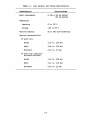
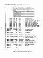
1.3 SPECIFICATIONS
General specifications for the OPP are given in Table 1-1.
peripheral signal specifications.
1-1
Table 1-2 gives
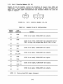
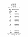
FIGURE 1-1.
Dual Parallel Port Module
TABLE 1-1.
n.tal Parallel Port Module Specifications
CHARACTERISTIC
SPECIFICATIONS
Power requirements
+5 Vdc @ 762 mA typical
991 mA maximum
Temperature
Operating
00 to 100 C
Storage
-40° to 85° c
Relative humidity
0% to 90% (non-condensing)
Physical characteristics
PC board only
Height
6.30 in. (160 nun)
Depth
3.94 in. (100 nun)
'Ihickness
0.59 in. (15 nun)
PC board with connectors
and board stiffener
Height
7.40 in. (188 nun)
Depth
5.12 in. (130 mm)
'Ihickness
0.83 in. (21 mm)
1-3
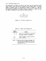
TABLE 1-2.
SIGNALS
(1)
PlPAO-PlPA7,
PlPBO-PlPB7,
P2PAO-P2PA7,
P2PBO-P2PB7,
PlCAl-PlCBl,
P2CA1-P2CB1
Peripheral Signal Specifications
CHARACTERISTIC
SPECIFICATIONS
High level input voltage
2 volts de minimum
I.ow level input voltage
a.a
High level output voltage with
!OH= -15 mA
2 volts de minimum
I.ow level output voltage with
IOL = 24 mA
o.s
Off state output current with
high level output voltage
applied
10
Off state output current with
low level output voltage
applied
-200
High level input current with
VIH = 2.7 volts de
20
I.ow level input current with
VIL = 0.4 volts de
-0.2 mA maximum
volts de maximun
volts de maximum
uA
maximum
uA
uA
maximum
maximum
NOTE:
(1) Refer to schematic diagram. Peripheral signals PlCA2,PlCB2, P2CA2,
and P2CB2 have the same specifications except that the off state
characteristics do not apply. '/m.y of the signals that are configured
as inputs (except PXCAl and PXCBl) should not be allowed to float;
therefore, any input signals not driven by the peripheral should be
held in either a high state or a low state.
1-4
1.4 GENERAL DESCRIPTION
'Ihe DPP is an I/O Channel-compatible dual printer interface module. 'Ihis module
confonns to the single-wide VME board fonn factor and connects to the I/O
Channel with a 64-pin DIN standard connector. 'Ihe DPP is used to expand the
resources of an I/O Channel master to include two printer interfaces, one
printer interface and a general-purpose 16-bit parallel data I/O port, or two
general-purpose 16-bit parallel data I/O ports.
PIA's (with buffers on their peripheral sides) are employed to implement the
two parallel data ports. In addition to having an I/O Channel interface, each
of the PIA's is capable of driving up to two of the I/O Channel interrupt lines.
A front panel FAIL LED indicator is provided to indicate a module malfunction.
'1\-.o
The user must provide a connector-compatible I/O Channel backplane or ribbon
cable for DPP connection to the I/O Channel master. Refer to the I/O Channel
Specification Manual, ~torola publication number M68RIOCS, for interfacing and
backplane information. 'Ihe user must also provide compatible cables for DPP
connection (via front panel connectors) to peripheral devices.
1.5 RELATED DOCUMENTATION
'Ihe Input/Oltput Channel Specification Manual, M68RIOCS, is applicable to the
DPP.
1-5/1-6
CHAPTER 2
HARrWARE PREPARATION AND INSTALIATION INS'IRUCTIONS
2.1
INTRODUCTION
'Ibis chapter provides tmpacking, hardware preparation,
instructions for the I:Ual Parallel Port Module.
2.2
and
installation
UNPACKING INS'IRUCTIONS
NOTE
If shipping carton is damaged upon receipt,
request carrier's agent be present during
tmpacking and .inspection of equipnent.
lbpack equipnent from shipping carton. Refer to packing list and verify that
all items are present.
Save packing material for storing or reshipping the
equipnent.
2.3
HARil4/ARE PREPARATION
'Ibis section describes the hardware preparation of the DPP module prior to
system installation. 'lhe DPP has been factory tested for system operation and
is shipped with factory-installed junpers.
'lhese factory-installed jlltlper
connections should be verified to ensure that the components are properly
configured for system operation. '!he DPP is configured to interface the I/O
Cllannel master with Centronics printer-compatible equipnent.
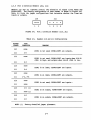
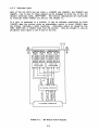
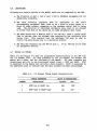
'!here are 13 headers on the DPP, as shown in Figure 2-1. 'Ibey are J2-J6 and
J8-Jl5. Table 2-1 lists each header, its function and factory-installed jlltlper
configuration.
For signal names such as PlCA2, etc., refer to the schematic diagram.
2-1
JS
..
J4
l
J8
CJ
J9
CJ
l
Ji
JIO
D~r 0
Jt2
II
J11D
l
J••D
Jt5
c____.
FIGURE 2-1.
DPP Module Header I.Dcation Diagram
Jt3
TABLE 2-1.
HFADER
NUMBER
OPP ftt>dule Headers
FUNCTION
FACTORY
CONFIGURATION
J2
LED monitor
2-3
J3
FOrt 1 (PlCA2, PlPAO-PlPA7) direction
1-2
J4
FOrt 1 (PlCA2, PlPAO-PlPA7) direction
1-2
JS
FOrt 1 (PlCB2, PlPBO-PlPB7) direction
1-2
J6
FOrt 1 (PlCB2, PlPBO-PlPB7) direction
JS
FOrt 2 (P2CA2, P2PAO-P2PA7) direction
1-2
J9
FOrt 2 (P2CA2, P2PAO-P2PA7) direction
1-2
JlO
FOrt 2 (P2CB2, P2PBO-P2PB7) direction
1-2
Jll
FOrt 2 (P2CB2, P2PBO-P2PB7) direction
No
Jl2
Interrupt select
2-4, 7-9
Jl3
Interrupt select
3-5, a-10
Jl4
Base address select
No
JlS
LED control
2.3.1
No
jumper
jumper
jumper
2-3
LED .r.t:>nitor Header (J2)
Header J2 is junpered between pins 2 and 3, as shown in Figure 2-2, and should
not be altered.
J2
1
0
2
I
3
FIGURE 2-2.
LED r-t>ni tor Header (J2)
2-3
2.3.2
Port 1 Direction Headers (J3, J4)
Headers J3 and J4 together control the direction of signal lines PlCA2 and
PlPAO-PlPA7. 'Ihe factory configuration of each header is shown in Figure 2-3.
Table 2-2 lists the jumper configurations that determine whether the lines are
inputs or outputs.
J3
1
J4
2
0---0
o
o
1
3
4
2
I
FIGURE 2-3.
Port 1 Direction Headers (J3, J4)
TABLE 2-2.
Headers J3 and J4 Configurations
HEADER
JUMPER
PINS
CONNECTED
J3
none
J4
1-2
J3
none
RF.MARKS
PlCA2 is not used; PlPAO-PlPA7 are outputs.
PlCA2 is not used; PlPAO-PlPA7 are inputs when U8-39
(CA2) is high, and outputs when U8-39 (CA2) is low.
J4
2-3
J3
none
J4
3-4
J3
none
J4
1-2, 3-4
J3
none
J4
none
J3
1-2
J4
none
J3
1-2 (1)
J4
1-2 (1)
NOTE: (1)
Factory-installed jumper placement.
PlCA2 is an input; PlPAO-PlPA7 are inputs.
PlCA2 is an input; PlPAO-PlPA7 are outputs.
PlCA2 is not used; PlPAO-PlPA7 are inputs.
-------------------·---------------------------------PlCA2 is an output; PlPAO-PlPA7 are inputs.
PlCA2 is an output; PlPAO-PlPA7 are outputs.
2-4
2.3.3
Port 1 Direction Headers (JS, J6)
Headers JS and J6 together control the direction of signal lines PlCB2 and
PlPBO-PlPB7. '!he factory configuration of each header is shown in Figure 2-4.
Table 2-3 lists the jumper configurations that determine whether the lines are
inputs or outputs.
JS
J6
0--0
1
HEADER
JUMPER
I
2
0
1
0
0
0
2
3
4
I
FIGURE 2-4.
Port 1 Direction Headers (JS, J6)
TABLE 2-3.
Headers JS and J6 Configurations
PINS
CONNECTED
JS
none
J6
1-2
JS
none
REMARKS
PlCB2 is not used; PlPBO-PlPB7 are outputs.
·---------PlCB2 is not used; PlPBO-PlPB7 are inputs when US-19
(CB2) is high, and outputs when US-19 (CB2) is low.
J6
2-3
JS
none
J6
3-4
JS
none
J6
1-2, 3-4
JS
none
J6
none
JS
1-2
J6
none (1)
JS
1-2
J6
1-2
PlCB2 is an input; PlPBO-PlPB7 are inputs.
---
·-------PlCB2 is an input; PlPBO-PlPB7 are outputs.
PlCB2 is not used; PlPBO-PlPB7 are inputs.
--------
(1)
PlCB2 is an output; PlPBO-PlPB7 are inputs.
PlCB2 is an ouput; PlPBO-PlPB7 are outputs.
NOTE: (1)
Factory-installed jumper placement.
2-S
2.3.4
Port 2 Direction Headers (JS, J9)
Headers JS and J9 together control the direction of signal lines P2CA2 and
P2PAO-P2PA7. '!he factory configuration of each header is shown in Figure 2-5.
Table 2-4 lists the jwnper configurations that determine whether the lines are
inputs or outputs.
JS
1
HEADER
JUMPER
J9
2
o---<>
o
o I
1
3
4
2
FIGURE 2-5.
Port 2 Direction Headers (JS, J9)
TABLE 2-4.
Headers J8 and J9 Configurations
PINS
RF.MARKS
CONNECTED
JS
none
J9
1-2
JS
none
P2CA2 is not used; P2PAO-P2PA7 are outputs.
P2CA2 is not used; P2PAO-P2PA7 are inputs when Ul0-39
(CA2) is high, and outputs when Ul0-39 (CA2) is low.
J9
2-3
JS
none
J9
3-4
P2CA2 is an input; P2PAO-P2PA7 are inputs.
~~~~--------~-
JS
none
J9
1-2, 3-4
JS
none
J9
none
JS
1-2
J9
none
JS
1-2 (1)
J9
1-2 (1)
--------------------------------P2CA2 is an input; P2PAO-P2PA7 are outputs.
~------·---------~~-·---
P2CA2 is not used; P2PAO-P2PA7 are inputs.
-------
·------·----·---------·
P2CA2 is an output; P2PAO-P2PA7 are inputs.
P2CA2 is an output; P2PAO-P2PA7 are outputs.
NOTE: (1)
Factory-installed jumper placement.
2-6
2.3.5
Port 2 Direction Headers (JlO, Jll)
Headers JlO and Jll together control the direction of signal lines P2CB2 and
P2PBO-P2PB7. 'Ihe factory configuration of each header is shown in Figure 2-6.
Table 2-5 lists the jumper configurations that determine whether the lines are
inputs or outputs.
JlO
Jll
I
1
HEADER
JUMPER
2
o
o
o
o
1
2
3
4
I
FIGURE 2-6.
Port 2 Direction Headers (JlO, Jll)
TABLE 2-5.
Headers JlO and Jll Configurations
PINS
CONNECTED
JlO
none
Jll
1-2
JlO
none
REMARKS
P2CB2 is not used; P2PBO-P2PB7 are outputs.
P2CB2 is not used; P2PBO-P2PB7 are inputs when Ul0-19
(CB2) is high, and outputs when Ul0-19 (CB2) is low.
Jll
2-3
JlO
none
Jll
3-4
P2CB2 is an input; P2PBO-P2PB7 are inputs.
------------none
JlO
P2CB2 is an input; P2PBO-P2PB7 are outputs.
Jll
1-2, 3-4
JlO
none
Jll
none
·-------------P2CB2 is not used; P2PBO-P2PB7 are inputs ••
JlO
---1-2
(1)
P2CB2 is an output; P2PBO-P2PB7 are inputs.
Jll
none (1)
JlO
1-2
Jll
1-2
P2CB2 is an output; P2PBO-P2PB7 are outputs.
NOTE: (1)
Factory-installed jumper placement.
2-7
2.3.6
Interrupt Select Headers (Jl2, Jl3)
Headers Jl2 and Jl3 together determine which PIA signal or signals -- [IRQlA*] ,
[IRQlB*], [IRQ2A*], or [IRQ2B*] -- will drive which I/O Channel interrupt line
(INT1*-INT4*). One, any combination, or all of the PIA signals can be connected
to a single I/O Channel interrupt line at the same time, but a single PIA signal
should not be connected to more than one I/O Channel interrupt line.
The two headers comprise four sets of six contacts (1-6 and 7-12). Each set of
six contacts controls one PIA to I/O Channel connection.
The factory
configuration of each header is shown in Figure 2-7. Table 2-6 lists the jumper
configurations that determine PIA signal to I/O interrupt line connections.
Jl2
2
Jl3
4
6
8
10
0---0
0
0
0
0
0
0
0---0
1
3
5
7
FIGURE 2-7.
9
12
2
4
6
8
:I I
0
0
0
0---0
0
0---0
0
0
:I
1
3
7
9
11
11
5
10 12
Interrupt Select Headers (Jl2, Jl3)
2-8
TABLE 2-6.
HEADER
JUMPER
PINS
CONNECTED
RF.MARKS
[IRQlA*] connected to INT2*
Jl2
1-3
Jl2
2-4
Jl2
3-5
[IRQlA*] connected to INT3*
Jl2
4-6
[IRQlA*] connected to INT4*
Jl2
7-9
Jl2
8-10
[IRQlB*] connected to INTl*
J12
9-11
[IRQlB*] connected to INT3*
Jl2
10-12
[IRQlB*] connected to INT4*
Jl3
1-3
[IRQ2A*] connected to INT2*
Jl3
2-4
[IRQ2A*] connected to INT!*
Jl3
3-5 ( 1)
[IRQ2A*] connected to INT3*
Jl3
4-6
[IRQ2A*] connected to INT4*
Jl3
7-9
[IRQ2B*] connected to INT2*
Jl3
8-10 ( 1)
[IRQ2B*] connected to INTl*
Jl3
9-11
[IRQ2B*] connected to INT3*
Jl3
10-12
[IRQ2B*] connected to INT4*
NOTE: (1)
2.3.7
Headers Jl2 and Jl3 Configurations
( 1)
(1)
[IRQlA*] connected to INTl*
[IRQlB*] connected to INT2*
Factory installed jumper placement.
Base Address Select Header (Jl4)
Header Jl4 can be configured to have the DPP occupy any $10 byte block within
the first $100 byte block of the I/O Channel memory map (see Figure 4-2). E!ach
of ,the two ports appears twice in the $10 byte block. The factory configuration
of the header is shown in Figure 2-8. Table 2-7 lists the jumper configurations
that select the desired location within the I/O Channel memory map.
2-9
Jl4
I
2
4
6
8
0
0
0
0
0
0
0
0
1
3
5
7
I
Base Address Select Header (Jl4)
FIGURE 2-8.
TABLE 2-7.
Header Jl4 Configurations
PINS
CONNECTED
REMARKS
1-2, 3-4,
5-6, 7-8
Base address is $00
1-2, 3-4,
5-6
Base address is $10
1-2, 3-4,
7-8
Base address is $20
1-2, 3-4
Base address is $30
1-2, 5-6,
7-8
Base address is $40
1-2, 5-6
Base address is $50
1-2, 7-8
Base address is $60
1-2
Base address is $70
3-4, 5-6,
7-8
Base address is $80
3-4, 5-6
Base address is $90
3-4, 7-8
Base address is $AO
3-4
Base address is $BO
5-6, 7-8
Base address is $CO
5-6
Base address is $DO
7-8
Base address is $EO
none (1)
NOTE: (1)
Base address is $FO
Factory-installed jumper placement.
2-10
2.3.8
LED Control Header (Jl5)
The configuration of header Jl5 controls front panel FAIL LED indicator DSl and
signal [PlPB7]. When the LED can be turned on by the [LED] signal, the [PlPB7]
signal is disabled (refer to the schematic diagram in Chapter 5) • When the
[PlPB7] signal is enabled, the [LED] signal is low and will hold the LED off.
The factory configuration of the header is shown in Figure 2-9. Table 2-8 lists
the jumper configurations that select the desired condition.
JlS
o
o--o
ol
1
2
4
3
FIGURE 2-9.
LED Control Header (JlS)
TABLE 2-8.
Header Jl5 Configurations
PINS
CONNECTED
REMARKS
2-3 (1)
FAIL LED is functionally operational
and signal [PlPB7] is disabled.
1-2
3-4
Signal [PlPB7] is enabled and FAIL
LED is disabled.
NarE: (1) Factory-installed jumper placement. If
J6-l and 2 are connected and JlS-2 and
3 are connected, then JlS-4 should be
connected to JlS-3.
2-11
2.4
INSTALLATION INSTRUcrIONS
When the DPP has been conf igurerl as desi rerl by the user, it is ready to be
installerl in a VME chassis or an I/Qncrlule 5-slot card cage.
2.4.1
Installation in VME Chassis
The DPP is installed in a VME chassis as follows:
a. Turn all equipment power OFF.
CAUTION
CONNECTING MODULES WHILE POWER IS APPLIED MAY
RESULT IN DAMAGE TO COMPONENTS ON THE MODULE.
b. Insert DPP in any single-width card slot.
c. Secure in place with two captive screws.
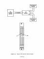
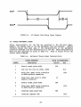
d. Peripheral connection to DPP port 1 arrl/or port 2 is accomplisherl by
mating a double-row, 50-pin, female ribbon connector, such as a 3M
3425-5000, to male connectors Jl arrl Jl6 on the DPP front panel, as shown
in Figure 2-10.
Printer cable assembly, Motorola part number
M68KVMPR'ICE, can be used. Connect the other errl of the ribbon cable to a
printer with a Centronics printer-canpatible interface.
e. Equipnent power may be turned ON.
2.4.2
Installation in 5-Slot I/Qnodule Card Cage
The DPP is installed in a 5-slot I/Qnodule card cage as follows:
a. Turn all equipment power OFF.
CAUTION
CONNECTING MODULES WHILE POWER IS APPLIED MAY
RESULT IN DAMAGE TO COMPONENTS ON THE MODULE.
b. If card cage in part of VERSl\module chassis, remove card slot cover
plate.
c. Insert DPP in slot and secure with two captive screws.
d. Peripheral connection to DPP port 1 and/or port 2 is accanplisherl by
mating a double-row, 50-pin, female ribbon connector, such as a 3M
3425-5000, to male connectors Jl and Jl6 on the DPP front panel, as shown
in Figure 2-10.
Printer cable assembly, Motorola part number
M68KVMPR'ICE, can be userl. Connect the other errl of the ribbon cable to a
printer with a Centronics printer-canpatible interface.
e. Equipment power may be turnerl ON.
2-12
CENTRONICS
PRINTER
1/0
CHANNEL
MASTER
1/0 CHANNEL
OPP
P1 MODULE
J1
J16
CENTRONICS
PRINTER
FAILQ
/~
J1,.......-
~Jt.
S~,.
I
J16
MVME410
FIGURE 2-10.
Typical OPP Interface Cabling Diagram
2-13/2-14
CHAPTER 3
OPERATIN:l INSTRUCTIONS
3.1
INTRODUCTION
'Ihis chapter provides the necessary information to initialize and operate the
Dual Parallel Port ~dule in a typical system.
3.2
INDICATOR
'The DPP contains one indicator ~ a front panel red FAIL LED. If header Jl5 is
jumpered between pins 2-3, the FAIL indicator will illuminate when an I/O
Channel reset or a software-controlled module failure occurs.
3.3 OPERATING PROCEDURE
Following is a typical procedure showing how to use the DPP to interface with a
Centronics printer.
a. Apply power to the system equipnent.
b. Select the printer.
c. If the VERSAmodule contains VERSAbug EPROM's, then the VERSAbug 2.0
Printer Attach (PA) corrunand can now be used.
d. Figure 3-1 is a typical driver routine that can be used to drive the
printer.
3-1
MOTOROLA M68000 ASM VERSION
1.30SMO:
5121.RTTLIO
.DRIVE~
.SA 08/121918214:52:12
**********************************************************************
1
2
3
4
5
6
7
*
8
9
**********************************************************************
*FUNCTION:
*printer.
*INPUT
14
21
22
23
24
25
26
27
28
29
38
31
32
33
34
35
36
37
38
39
4Q
41
42
43
44
45
46
47
INITIALIZATION ROUTlNE
Initializ"i! Parallel Port 1 of the RTTLIO fo1· driving a
11-
*
11-
*
NONE
PARAMET~RS:
*OUTPUT PARAMETERS: NONE
•
**********************************************************************
*
*REGISTERS ALTERED: NONE
11
12
15
16
17
18
19
20
1
****************************~*****************************************
10
13
VM02 RTTLIO PARALLEL PORT
**********************************************************************
**********************************************************************
00001000
00F801E1
00000000
00000004
00000002
00000006
00000002
00000006
00000008
8QUl000H
$1000
$FB01E1
$0
EGU
EGU
EGU
EGU
EGU
EGU
EGU
EGU
EGU
EGU
$6
PCNTRLA
PCNTRLB
PDATA
PDATB
START OF THIS PROGRAM
BASE ADDRESS OF PARALLEL PORT 1
OFFSET OF A SIDE PERIPHERAL DATA REG. FROM BASE
OFFSET OF B SIDE PERIPHERAL DATA REG. FROM BASE
OFFSET OF A SIDE CONTROL REGISTER FROM BASE
OFFSET OF B SIDE CONTROL REG. FROM BASE
OFFSET OF A SIDE STATUS REQISTER FROM BASE
OFFSET OF B SIDE STATUS REG. FROM BASE
OFFSET OF A SIDE DATA DIRECTION REG. FROM BASE
OFFSET OF B SIDE DATA DIRECTION REQ. FROM BASE
THISPR
0
A0,-<A7>
SR,-CA7>
GET SOME WORKING REGISTERe
SAVE 6S800 STATUS REQ
PBASE,A0
POINT Aa AT PORT 1
0009100A 117C883aeaaa JNITDDRA MOVE.B
MOVE.I
ee0e101e laBCQKIFF
H3B,PCNTRLACA0>
l•FF,PDDRACA8>
POINT AT DDRA
DDRA MAKES PERPH DATA A OUTPUTS
e0e01014 11 7CfZHl3Clllll2 INITCTRA MOVE. B
. .3C,PCNTRLA<A0>
0000101A 117C00380906 JNITDDRB MOVE.B
HOVE.8
0011011128 117C01180Cl004
H38,PCNTRLBCA0>
. .a11,PDDRB<A0)
111111111 1126 117Cll03Cll1106 INITCTRB HOVE.I
tt•3C,PCNTRLB<A0>
00081000
00001000 00000008
88801800 2F88
eeee1ee2 40E7
THISPR
PB ASE
PDATA
PDATB
PCNTRLA
PCNTRLB
PSTATA
PST ATB
PDDRA
PDDRB
$4
$2
ORG
INITPIA DS.W
INIT&AVE MOVE.L
MOVE.W
LEA
881181884 41F98aFB81E1
•
*
0000102C 46DF
0800102E 205F
00001030 4E75
JNITRSTR HOVE. W
HOVE.L
CA2=0UTPUTCHIGH RIGHT NOW>, SET FLAG
ON LOW TO HIQH, INT DISABLED
POINT AT DDRB
DDRB MAKES PERPH DATA B INPUlS
CB2•0UTPUTCHIGH RIQHT NOW), SET FLAQ
INT DISABLED
ON LOW TO HIQH,
<A7>+,SR
CA7>+, A8
RESTORE 68000 STATUS REQISTER
RESTORE Aa
RTS
FIGURE 3-1.
Typical Printer Driver Routine (Sheet 1 of 3)
MOTOiiOLA M68CIN ASt1 VERSION
49
58
1.3e5t1D
59.RTTLIO
.DRIVE~
.SA
08/~9/8214:52:12
**********************************************************************
*
51
52
Vt182 PRINTER DRIVER USING THF RTTL.IO PARALLF.L PCJkT 1
1:·
**********************************************************************
53
•FUNCTION: Send ·the character contained in l>fl to a Printer through
•an RTTLIO board(Board strapped to appear at Block 1~).
If the
54
55
*
*
•Printer is not selected then return ~~o• thi• subroutine with D!.B= *
•Non-zero.
If the printer is selected and the ch•r•cter is sent
*
•auccessful11:1 then return with Di. ll=-zeru
"*
56
57
58
**********************************************************************
•INPUT PARN1ETERS:
•BE SENT.
59
60
61
62
63
Dit.B
CONTAINS THE ASCII CODE OF THE CHARAClER TO*
*
**********************************************************************
•OUTPUT PARN1ETERS: BIT a OF D1 .. a IF THE PRINTER IS NOl SELECTED, *
•BIT 1 OF D1 m 1 IF THE PRINTER IS OUT OF PAPER.
D1.N; $01 IF
*
•THE PRINTER WAS SELECTED, WAS NOT OUT OF PAPER, AND THF CHARACTER
*
•WAS SENT SUCCESSFULLY.
IF NO ACKNOWLEDOE IS EVER RECIEVED THEN THIS*
•ROUTINE IS NEVER EXITED.
*
64
615
66
67
**********************************************************************
*
•REOISTERS ALTERED: D1.B
68
69
70
**********************************************************************
71
1'
w
72
73
74
715
76
77
78
79
8~
81
82
83
84
85
86
87
00
89
90
91
92
PAC KN
PSTRI
PRDV
EGU
EGU
EGU
PST AT A
PCNTRLA
PDATB
PC HAR
PSAVE
DS.W
t10VEt1.L
l10VE.W
a
D2/A0,-<A7>
SR,-<A7>
QET SOt'IE WORKINQ REQISTERS
SAVE 68'INl8 STATUS REOISTER
eeee1e3s 41F9G1GJF8a1E1
LEA
PBASE,A0
A0aBASE ADDRESS OF PORT 1
0000103E
00001942
00001046
00001048
0000Ul4A
MOVE.I
AND.B
t10VE.B
SUB.B
BNE.S
PRDY<Aczt>,D2
1x00aa0911,n2
D2.D1
••01,02
PRSTR
QET THE STATUS OF PAPER AND SELECT
PAPER OUT•BIT 11SELECT=BIT 0
SAVE RESULTS IN Dl AS OUTPUT PARAt1ETER
IF PRINTER NOT SELECTED OR PAPER OUT
THEN RETURN WITH D1.Dl•01<ERROR>
GH1!HlllW2
MNHMIGMl2
eaMHH
aaee1aa2 awaaaa
aaaa1aa2 48E7211811
eeaa1e36 4flE7
14280004
02020aa3
1202
5392
6618
OFFSET OF A SIDE STATUS REO. FROt1 BASE
OFFSET OF A SIDE CONTROL. REQ. FROt1 BASE
OFFSET OF B SIDE PERIPHERAL. DATA REO. FROH BASE
0000104C 1080
PSEND
t10VE.B
D0.PDATA<AB>
ELSE SEND CHARACTER TO PRINTER
0flee104E 1419
PACKNCLR t10VE.B
PDATA<A0>,D2
DO DUt1t1Y READ OF PIA PERIPHERAL DATA
REQISTER IN ORDER TO CLEAR ACKNOWLEQDE FLAO
*
FIGURE 3-1.
Typical Printer Driver Routine (Sheet 2 of 3)
93
94
95
96
97
98
99
100
101
102
103
00001050 117C00340002 PSTROBE
00001056 117C003C0002
MOVE.B
MOVE.B
#$34,PSTRB<A0>
H3C,PSTRB<A0>
MAKE DATA STROBE GO LOW
THEN HIGH
0000105C 082800070002 PACKNQE
00001062 67F8
BTST.B
BEO.S
#7,PACKNCA0>
PACKNGE
IF CHARACTER NOT ACKNOWLEDGED
THEN WAIT FOR IT TO BE
00001064 46DF
00001066 4CDF0104
PRSTR
MOVE.W
MOVEH.L
<A7).+, SR
<A7)+,D2/A0
RESTORE 68000 STATUS REQISTER
RESTORE REGISTERS
0000106A 4E75
PRTRN
RTS
104
END
105
MOTOROLA M6B000 ASM VERSION
1.30SMD
00.RTTLIO
DRIVER
.SA
0B/09/B214:~2:12
SYMBOL TABLE LISTING
SYMBOL NAME
INITCTRA
JNITCTRB
INITDDRA
INITDDRB
INITPIA
INITRSTR
INITSAVE
PAC KN
PACKNCLR
PACKNQE
PB ASE
PC HAR
PCNTRLA
PCNTRLB
SECT
VALUE
00001014
00001026
0000100A
0000101A
00001880
0000102C
00001000
00000002
0000104E
01Z100185C
00F801E1
01Z1001832
00000002
IHICl08886
FIGURE 3-1.
SYMBOL NAME
PDATA
PDATB
PDDRA
PDDRB
PRDY
PRSTR
PRTRN
PSAVE
PSEND
PSTATA
PSTATB
PSTRB
PSTROBE
THISPR
SECT
VALUE
00000000
00000004
00000000
00000004
Ci!UD000004
00001064
0000106A
00001032
0000104C
00000002
00000006
00000002
00001050
a0001m00
Typical Printer Driver Routine (Sheet 3 of 3)
CHAPTER 4
FUNCTIONAL DESCRIPl'ION
4.1
INTRODUCTION
'Ibis chapter provides the overall block diagram level descriptions for the n.tal
Parallel Port fvk>dule. A general description provides an overview of the module,
followed by a detailed description of each section of the DPP.
4.2 GENERAL DESCRIPl'ION
'!he DPP is designed to provide a parallel interface between an I/O Channel (bus)
master and one or two printers, with a Centronics interface.
The DPP employs an MC6821 chip to latch output printer data, drive printer
control lines, and monitor printer handshake and status lines. '!be MC6821 data
sheet contains additional infonnation on the MC6821.
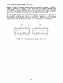
The DPP provides two general-purpose, parallel, printer ports. Figure 4-1 is a
block diagram of the DPP. As shown in Figure 4-1, the DPP has a conmon I/O
Channel interface section and two parallel port sections. F.ach of the parallel
port sections consists of a peripheral interface adapter (PIA) with TTL buffers
that provide drive capability on the peripheral side. 'Ihe two parallel ports
are identical except for a FAIL LED indicator that is strappable to port 1.
4.3
I/O CHANNEL INTERFACE
'Ihe I/O Channel interface section provides map decoding logic, access control
logic, and interrupt logic. An explanation of each follows.
4. 3 .1 Map Decoding Logic
'Ihe DPP is strap-selectable to appear at any $10 byte block within the first
$100 byte block of the I/O Channel memory map, as shown in Figure 4-2. If the
selected base address is $CO the $10 block byte upper boundary is one bit less
than $DO.
Each port appears ·twice in the $10 byte area.
'lb set the base
address of the DPP, see block select header Jl4 infonnation in Cllapter 2.
Table 4-1 shows the addresses of the registers within each of the DPP parallel
ports with respect to the DPP base address.
4.3.2 .Access Control U:>gic
'Ihe access control logic provides an asynchronous I/O Channel to a synchronous
MC68B21 interface. 'Ihe interface operation is transparent to ·software on the
I/O Channel master.
4-1
4.3.3
Interrupt Logic
Fach of the two PIA's has two lines -- [IRQlA*] and [IRQlB*], and [IRQ2A*] and
IRQ2B*]. Ole or more of these signals can be strapped to drive one of the I/O
Channel interrupt lines, INT1*-INT4*. 1he various combinations are controlled
by interrupt select headers Jl2 and Jl3 (see Chapter 2) •
If a port is connected to a printer i it may be software configured to drive
[IRQlA*] when the printer gives an acknowledge, and/or to drive [IRQlB*] wheri
the printer indicates a fault condition.
Interrupts cannot be caused by the
BUSY, PAPER OUT, or SELECT lines from the printer. 1hey are brought in only as
peripheral data inputs to the B side of the PIA.
~
VI
0
a:
1/0 CHANNEL INTERFACE
1/0 CHANNEL CONNECTOR
FIGURE 4-1.
OPP flk:>dule Block Diagram
4-2
$0100
$00FO
$00EO
$0000
$00CO
The DPP is jumper-selectable
$0080
to appear at any $10 byte
$00AO
block of memory in this area.
$0090
$0080
$0070
$0060
$0050
$0040
$0030
$0020
$0010
$0000
FIGURE 4-2.
I/O Channel Memory Map
4-3
TABLE 4-1.
OFFSET FRCM
DPP MODULE
BASE ADDRESS
F
E
E
D
c
c
B
A
A
CONTROL
REGISTER BIT
-----------CRB-2
CRA-2
x
x
x
x
0
1
x
0
1
x
x
x
x
9
x
x
x
x
8
0
X·
8
1
7
5
x
x
x
x
x
x
4
0
4
1
3
1
x
x
x
x
0
0
0
1
6
6
2
2
NOTE:
DPP M:>dule Register Addresses
0
1
x
0
1
x
x
x
x
0
1
x
x
x
REGISTER
PORT #
Control register B
rata direction register
Peripheral register B
Control register A
Data direction register
Peripheral register A
Control register B
r:ata direction register
Peripheral register B
Control register A
IBta direction register
Peripheral register A
Control register B
r:ata direction register
Peripheral register B
Control register A
Data direction register
Peripheral register A
Control register B
rata direction register
Peripheral register B
Control register A
Data direction register
Peripheral register A
2
2
2
2
2
2
X denotes a don't care condition.
4-4
B
A
1
B
1
1
1
A
1
1
B
A
2
2
2
2
2
2
1
B
1
1
1
A
1
1
4.4
PARALLEL PORT 1
Parallel port 1 employs an MC68B21 {PIA) for its logic functions. '!he MC6821
Data Sheet explains how to use it. Pay particular attention to the sections
that deal with progranuning the PIA. In addition to the infonnation provided in
the PIA manual, the following infonnation is necessary to use the DPP.
All the peripheral data and peripheral control lines on the PIA are buffered
with TrL drivers/receivers.
Because these lines are buffered, care must be
taken to make the directions of the peripheral line coming from the PIA
compatible with the direction of the buffer on that line.
CAl {US-40) and CB! {US-18) are buffered to become PlCAl and PlCBl,
respectively.
'!heir buffers are always inputs, as defined by the PIA;
therefore, no buffer fight can ever exist on these lines.
CA2 {US-39) and CB2 {US-19) are buffered to become PlCA2 and PlCB2,
respectively. Each one can be progranuned as an input or as an output in the
PIA. Each PIA TrL buffer is hardware strappable as an input or as an output.
'lherefore, the possibility of a buffer fight exists for one case only -- when
the line is progranuned as an output by the PIA and its TrL buffer is strapped as
an input. Consequently, the progranuned direction of the line and the strapped
direction of the line should be the same. For direction strapping, see the port
1 infonnation in Chapter 2.
PAO-PA? are buffered to become PlPAO-PlPA7, respectively. 'Ihe direction of each
one of these lines is individually progranunable within the PIA. lbwever, the
direction of their buffers is not individually strappable in hardware.
'!he
buffers for these lines are strapped as either all inputs or as all outputs, or
they are strapped so that their direction is an input when CA2 is at a logic
high or an output when CA2 is at a logic low. '!he possibility for a buffer
fight exists for any case in which a line is programmed as an output and the
buffers are strapped/programmed as inputs.
'!he progranuned direction of the
lines and the strapped/programmed direction of the buffers should be the same.
For direction strapping, see the port 1 infonnation in Chapter 2.
PBO-PB7 relate to PlPBO-PlPB7 in the same way that PAO-PA? relate to PlPAO-PlPA7
with the following exception. When JlS is strapped such that [PB7] controls the
FAIL LED indicator, then PB7 is severed from [PlPB7] , and it may be programmed
as an output even though the direction of the PlPBO-PlPB7 buffers may be inputs.
In this configuration, driving PB7 low turns on the FAIL LED and driving PB7
high turns off the FAIL LED.
4.5
PARALLEL PORT 2
Parallel port 2 is identical to parallel port 1 except that port 2 does not have
a FAIL LED indicator connectable to PB?. 'Iherefore,.the special case covered in
the port 1 explanation with respect to the LED does not apply to port 2.
4-5
4.6
LIMITATIONS
Following are certain options of the MC6821 which are not supported by the DPP.
a. 'Ihe direction of port 1 CA2 or port 2 CA2 is hardware strappable but not
dynamically alterable.
b. 'Ihe data direction registers must be configured to set their
corresponding peripheral data lines to be a block of eight inputs or a
block of eight outputs, depending on the hardware option that is being
used. 'Ihe direction of individual peripheral data lines is not allowed
to differ from that of the whole set of eight peripheral data lines.
c. 'Ihe Read Strobe with E Restore mode of the PIA will cause a 250-ns pulse
that is shorter than the minimum time required by the Centronics data
strobe line.
'!his requires that the Set/Reset CA2 mode be used to
control the data strobe line to a Centronics printer.
d. 'Ihe FAIL LED indicator may use PB7 of port 1.
for peripheral devices.
If so, PB7 may not be used
4.7 MODULE I/O TIMII:-Ki
Table 4-2 and Figure 4-3 show the performance characteristics of the DPP from
the I/O Channel side. All data transfers on the I/O Channel are between the
master and a slave, and are initiated by the master. All data transfers are
asynchronous and rely on two interlocked signal lines -- STB* and XACK*. STB*
is generated by the master and initiates a data transfer. XACK* is generated by
the addressed slave to indicate that the data transfer has been acknowledged.
TABLE 4-2.
I/O Channel Timing Signal Characteristics
NUMBER
TIMING PARAMETER
DESCRIPTION
VALUE IN NANOSECONDS
TYPICAL
MAX
1
STB* low to XACK* low
990
1300
2
STB* high to XACK* high
122
184
4-6
STB*
XACK*
FIGURE 4-3.
I/O Channel Side Timing Signal Diagram
4.8 MODULE PERIPHERAL TIMING
Timing characteristics for the PIA are contained in the PIA data sheet.
However, the signals used on the DPP peripheral side are buffered.
Buffers
introduce delays that make some of the characteristics at the peripheral
connectors different from the characteristics at the PIA. '!hose characteristics
which are most important are given in Table 4-3. Refer to Figure 4-4 for the
related timing diagrams.
TABLE 4-3.
Peripheral Timing Signal Characteristics
VALUE IN NANOSECONDS
TYPICAL
MAX
NUMBER
TIMING PARAMETER
DESCRIPTION
1
Cbntrol output pulse width
2
Rise and fall time for PXCBl, PXCB2
N/A
3
Delay time, PXCAl active transition
to PXCA2 :EX>Sitive transition
1036
4
Delay time, data valid to PXCB2
negative transition
5
Cbntrol output pulse width
6
Delay time, PXCBl active transition
to PXCB2 positive transition
7
Interrupt input pulse time
8
Interrupt response time
250
14
250
1036
500
1025
4-7
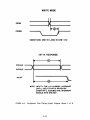
READ MODE
PXCA2
CONDITIONS: CONTROL REGISTER A, BIT 5
(CRA-5) • CRA-5 •I, CRA-4• 0
READ MODE
PXCAI
PXCA2
CONDITIONS: CRA-5• I 1 CRA-5• CRA-4•0
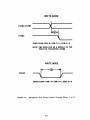
FIGURE 4-4.
Peripheral Side Timing Signal Diagram (Sheet 1 of 3)
4-8
WRITE MODE
PXPBO-PXPB7
PXCB2
CONDITIONS; CRB-5 • CRB-1•I,CRB-4•0
NOTE: C82 GOES LOW AS A RESU~T OF THE
POSITIVE TRANSITION OF LE]
WRITE MODE
PXC82
CONDITIONS: CRB-5 • CRB-l•l,CRB-4• 0
FIGURE 4-4.
Peripheral Side Timing Signal Diagram (Sheet 2 of 3)
4-9
WRITE MODE
PXCBI
PXCB2
CONDITIONS: CRB-5• I, CRB-l•CRB-4•0
I NT* RESPONSE
PXCAl,2
INTX*
NOTE! INTX* •THE 1/0 CHANNEL INTERRUPT
(INT I- INT 4) THAT IS DRIVEN BY
[IRQX*/B*J, ASSUMES THE INTERRUPT
ENABLE BITS ARE SET
FIGURE 4-4.
Peripheral Side Timing Signal Diagram (Sheet 3 of 3)
4-10
CHAPTER 5
SUPPORT INFORMATION
5.1
INTRODUcrION
This chapter provides the connector signal descriptions, parts list and
associated parts location diagram, and a schanatic diagram for the Dual Parallel
Port Module.
5.2 CONNECTOR SIGNAL DES:::RIPTIONS
The OPP has three interface connectors -- one to connect it to the I/O Channel
arrl two to connect it to Centronics printer-canpatible interface peripheral
devices.
5.2.1
I/O Channel Connector
The I/O Channel connector Pl on the OPP is a standard DIN 41612 triple-row,
64-pin, male connector. The backplane/ribbon cable uses the fanale connector.
Table 5-1 lists the connector Pl pin assignments.
.Additional information on
this connector can be obtained from the I/O Channel Specification Manual.
5.2.2
Peripheral Connectors
Front panel connectors Jl arrl J 16 on the
connectors. They mate to a fanale ribbon
Table 5-2 lists the front panel connectors
number, signal mnemonic, and signal name arrl
5.3
OPP are double-row, 50-pin, male
connector such as a 3M 3425-5000.
Jl arrl Jl6 pin assignments by pin
description.
PARTS LIST
Table 5-3 lists the components of the OPP. A parts location diagram for the
mcrlule is provided in Figure 5-1. This parts list reflects the latest issue of
OPP mcrlule at the time of printing.
5.4
DIAGRAMS
Figure 5-2 is the schanatic diagram for the DPP.
5-1
TABLE 5-1.
I/O Connector Pl Pin Assignments
PIN
NUMBER
SIGNAL
MNEMONIC
Al-AlO,
Al7-Al9,
A24,A25,
A31,A32,
GND
GROUND
All
All
ADDRESS bus (bit 11) - cne of 11 input signals used to
selectively access the DPP.
Al2
AlO
ADDRESS bus (bit 10) - Same as bit All on pin All.
Al3
AB
ADDRESS bus (bit 8) - Same as bit All on pin All.
Al4
A6
ADDRESS bus (bit 6) - Same as bit All on pin All.
Al5
A4
ADDRESS bus (bit 4) - Same as bit All on pin All.
Al6
A2
ADDRESS bus (bit 2) - Input signal used to select port
1 when low and port 2 when high during a OPP cycle.
A20
D7
Jl\TA bus (bit 7) - Bidirectional signal used to transmit
data between the I/O Channel master and the OPP during
read and write cycles.
SIGNAL NAME AND DESCRIPTION
c11,c20,
C25,C31,
C32
A21
D6
Jl\TA bus (bit 6) - Same as bit D7 on pin A20.
A22
04
Jl\TA bus (bit 4) - Same as bit D7 on pin A20.
A23
02
Jl\TA bus (bit 2) - Same as bit D7 on pin A20.
A26,C26
-12v
Not used by DPP.
A27,
CS-ClO,
C27
(Reserved)
Not used by DPP.
A28,C28
+12V
Not used by DPP.
A29,A30,
C29,C30
+5V
+5 Vdc Power - Used by the module logic circuits.
Cl
INT4*
INTERRUPT REQUEST 4 - cne of four active low output
signal lines used by the DPP to interrupt the I/O
Channel master.
C2
INT3*
INTERRUPT REQUEST 3 - Same as signal INT4* on pin Cl.
C3
INT2*
INTERRUPT REQUEST 2 - Same as signal INT4* on pin Cl.
5-2
TABLE 5-1.
PIN
NUMBER
SIGNAL
MNEMONIC
I/O Connector Pl Pin Assigrunents (cont'd)
SIGNAL NAME AND DESCRIPTION
C4
INTl*
INTERRUPT REQUEST 1 - Same as signal INT4* on pin Cl.
cs
!ORES*
INPUT/OUTPUT RESET - Active low input signal used to
reset the DPP.
C6
XACK*
TRANSMIT ACKNCl'/LEIXiE - Active low output signal used to
advise the I/O Channel master that write data is latched
or read data is available.
CLK
CLOCK - Free-running input signal used by the DPP for
internal synchronization and timing.
Cl2
A9
ADDRESS bus (bit 9) - Same as bit All on pin All.
Cl3
A7
ADDRESS bus (bit 7) - Same as bit All on pin All.
Cl4
AS
ADDRESS bus (bit 5) - Same as bit All on pin All.
ClS
A3
ADDRESS bus (bit 3) - lt>t used.
Cl6
Al
ADDRESS bus (bit 1) - Same as bit All on pin All.
Cl7
AO
ADDRESS bus (bit 0) - Same as bit All on pin All.
Cl8
STB*
STROBE - The high to low transition of this .input signal
indicates to the DPP that an I/O Cllannel cycle is
starting. The low to high transition indicates to the
DPP that the current I/O Channel cycle has ended.
Cl9
WT*
WRITE - An input signal that is low when the I/O Channel
is in a write cycle, and high when the I/O Channel is in
a read cycle.
C21
DS
IY\TA bus (bit 5) - Same as bit D7 on pin A20.
C22
D3
IY\TA bus (bit 3) - Same as bit D7 on pin A20.
C23
Dl
IY\TA bus (bit 1) - Same as bit D7 on pin A20.
C24
DO
IY\TA bus (bit 0) - Same as bit D7 on pin A20
5-3
TABLE 5-2.
PIN
NUMBER
1
Peripheral Connectors Jl arrl Jl6 Pin Assigrnnents
SIGNAL
MNEMONIC
PXCB2
SIGNAL NAME AND DESCRIPTION
INPUT PRIME - A low-level output signal which clears the
printer buffer arrl initializes the logic.
(Not used by
all printers)
GROUND
2-6,
10-50
(even
numbers)
3
Gm
GROUND
5
PXCBl
FAULT - A low-level input signal that irrlicates a printer
fault condition such as paper enpty; light detect, or a
deselect corrlition. (Not used by all printers)
7,41,
45,49
(Reserved)
8
(None)
No connection.
9
PXPB7
N/A
11
PXPB6
N/A
13
PXPBS
N/A
15
PXPB4
N/A
17
PXPB3
N/A
19
PXPB2
BUSY - An input signal indicating that the printer cannot
receive data.
21
PXPBl
OOT OF PAPER - A high-level input indicating the printer
is out of paper.
23
PXPBO
SELECI' - A high-level input signal indicating that the
printer is selecterl.
25
PXPA7
PERIPHERAL DATA LINE (PD8) - OUtput data to printer fran
PA7 of PIA.
27
PXPA6
PERIPHERAL DATA LINE (PD7) - Same as pin 25 except bit AG.
29
PXPAS
PERIPHERAL DATA LINE (PD6) - Same as pin 25 except bit AS.
31
PXPA4
PERIPHERAL DATA LINE (PDS) - Same as pin 25 except bit A4.
33
PXPA3
PERIPHERAL DATA LINE (PD4) - Same as pin 25 except bit A3.
35
PXPA2
PERIPHERAL DATA LINE (PD3) - Same as pin 25 except bit A2.
N/A
5-4
TABLE 5-2.
Peripheral Connectors Jl arrl Jl6 Pin Assignments (cont'd)
PIN
NUMBER
SIGNAL
MNEMONIC
37
PXPAl
PERIPHERAL DATA LINE (PD2) - Same as pin 25 except bit Al.
39
PXPAO
PERIPHERAL DATA LINE (PDl) - Same as pin 25 except bit AO.
43
PXCA2
DATA STROBE - An output pulse used to clock data fran the
MPU to the printer logic. The pulse is active low arrl at
least 1.0 us wide.
47
PXCAl
ACKN<mLEDGE - A low-level input pulse indicating the input
of a character into manory or the eoo of a functional
operation.
SIGNAL NAME AND DESCRIPTION
TABLE 5-3.
REFERENCE
DESIGNATION
OPP Module Parts List
MOTOROLA
PART NUMBER
DESCRIPTION
84-W8126B01
Printerl wiring board
Cl,C2,C3,C4,
C5,C6,C7,C8
215"W992C025
Capacitor, ceramic, .1 uF @ 50 Vdc
C9
23NW9618A33
Capacitor, electrolytic, 22 uF@ 25 Vdc
DSl
48NW9612A34
Indicator light, rerl, 5 Vdc
Jl
28NW9802D76
Connector, right angle, 50-pin
J2
28NW9802D04
Header, single-row post, 3-pin
J3,J5,J8,Jl0
28NW9802D01
Header, double-row post, 2-pin
J4,J6,J9,Jll,Jl5
28NW9802E30
Header, single-row post, 4-pin
J7
28NW9802E41
Connector, socket, 50-pin
Jl2,Jl3
28NW9802C63
Header, double-row post, 12-pin
Jl4
28NW9802C43
Header, double-row post, 8-pin
Jl6
28-W4262B01
Connector, socket, 50-pin
(Stackerl on Jl)
5-5
TABLE 5-3.
OPP Module Parts List (cont'd)
REFERENCE
DESIGNATION
MOrGROIA
PART NUMBER
DESCRIPTION
Pl
28NW9802EOS
Connector, plug, 64-pin
Rl,R2,R6
51NW9626A22
Resistor net\\10rk, S/lOk ohm
R3,R4,R5,R7
SlNW9626A37
Resistor network, 9/lOk ohm
Ul,U9,Ull,Ul2
SlNW9615E96
I.C. SN74LS24S
U2,U3,Ul7
SlNW961SF02
I.C. 74LS244N
U4
SlNW961SH93
I.C. SN74LS641N
us
SlNW961SH92
I.C. N74LS112N
U6
SlNW961SF41
I.C. LM74LS164N
U7
51NW961SH41
I.C. SN74LS682N
U8,Ul0
SlNW961SD8S
I.C. MC68B21P
Ul3
SlNW961SG38
I.C. SN74LS38N
Ul4
SlNW961SE93
I.C. SN74LS14N
UIS
SlNW9615Gl2
I.C. SN74LS37SN
Ul6
SlNW961SCS6
I.C. SN74S08N
Ul8
SlNW961SE98
I.C. SN74LS373N
09NW9811A22
Socket, I.e., DIL, 40-pin
(use at US and UlO)
29NW980SB17
Jumper, shorting, insulated
(use at J2-JS, J8-Jl0, Jl2, Jl3, JlS)
5-6
Jb
"b
aJ~~
0
DJr
UI
U1
I
1
OCI
J9
(
U2
Jib
Jll
l
RI
I~
C2
U3
U4
C4
"'V'"
U9
R3
Ul2
Ull
C6
Jl8
UIO
~
ce
Pl
0
Ul3
Ul4
R7
-c::::J-C7
FIGURE 5-1.
U7
Jl4D
Ul6
-c::::JI
l
0
R6
R4
R8
U6
_,,,,,,
0
U8
Jl3
C3
ue
JT
ex:>
0
11
Jl2
R2
-...J
........
U1
I
I
DPP Module Parts Location Diagram
Ul8
ce
Ul7
0
UIS
Ct
!.
2.
3.
&
5.
&
A
~
~
Pl - A29
Pl-C29
Pl-A30
> Pl-C30
Pl-Al
Pl-A2
Pl-A3
Pl-A4
Pl-A5
Pl-A6
Pl-A '7
> Pl-AB
Pl-A9
Pl-Al0
> Pl-Al7
> Pl-Al8
> Pl-Al9
> Pl-A24
Pl-A25
Pl-A31
Pl-A 32
> Pl-Cll
Pl-C20
P1-C25
Pl-C31
Pl-C32
*
6.
&
&
NOTES:
FOR REFERENCE DRAWINGS REFER TO
BILL(S) OF MATERIAL
UNLESS OTHERWISE SPECIFIED:
ALL RESISTORS ARE IN OHMS,:!. 5PCT,
114 WATT.
ALL CAPACITORS ARE IN UF.
ALL VOLTAGES ARE DC.
INTERRUPTED LINES CODED WITH THE
SAME LETTER OR LETTER COMBINATIONS
ARE ELECTRICALLY CONNECTED.
DEVICE TYPE NUMBER IS FOR REFERENCE
ONLY. THE NUMBER VARIES WITH THE
MANUFACTURER.
SPECIAL SYMBOL USAGE:
DENOTES - ACTIVE LOW SIGNAL.
Cl DENOTES - ON BOARD SIGNAL.
INTERPRET DIAGRAM IN ACCORDANCE
WITH AMERICAN NATIONAL STANDARDS
INSTITUTE SPECIFICATIONS, CURRENT
REVISION.
PART TYPES ARE ABBREVIATED IN
THE FIELD OF THE DRAWING. FOR
FULL PART TYPE, REFER TO TABLE I.
DENOTES PWB HEADER CONNECTOR.
DENOTES FRONT PANEL CONNECTOR.
DENOTES PWB-FRONT PANEL CONNECTOR.
~a~csic1icGLsL4ic3L2~c1
PWB
&
REF
DES
Jl-30
+5V
R'2A
I
lJ I
U2
U3
U4
U5
U6
U7
U8
U9
Ul0
Ull
Ul2
Ul3
Ul4
U15
Ul6
Ul7
U18
~K 2
·~
TYPE
&
74LS245
74LS244
74LS244
74LS641
74LSll2
74LS164
74LS268
MC68821
74LS245
MC68B21
14LS245
74LS245
74LS38
?+LSl4
14LS375
74S08
"74LS244
14LS373
GNO
+5V
10
2"
2121
20
10
10
I QJ
8
20
1
I QJ
I+
16
2eJ
I
2.QJ
10
I
10
10
7
"1
UJ
6
20
20
20
14
14
16
1
I+
"'
20
20
1(1
NC
Jl-412J
I
Jl-42
Jl-44
Jl-46
> J 1-48
J 1-SeJ
LS'Z.4
4
I
l~K 1¢
NC
NC
1¢1'\ 5
t-J----1\.IV\r-=--
}NC CRESERVEDl
R7E
I K G
)-Ne C-12.V)
tr
NC
NC
~~~
NC
PZCAZ
&
&
J7-41
ozcAI
:
J,J 77~43~ ~ ~
2GI
PZPA<b
J(
ZGI __,,P~2=PA~l,....--~--~----J=7-~3-.7~<
ZGI --=P~2=P~A2~~-----J_7-_3~5~(
2 6 'I __,_P-=2"'-'PA"-'3..___ _ _ _ _J.;;_7.;_--=3'-=<3(
P2PA4J 7-31
P2PA5
J7-29~
2 c;,
2G\ -':~~~--1--~~J~7-~2~7~.
1
2GI ---~~-----~-J_7-~2~5~
J7-23
Jl6-8~
__,,..-...:.o=----f-------~-<
-6
JIG-14
Jl6-37
JIG-35
> JIG-16
> JIG-18
JIG-i~
lll 6-::.Z,:Z
JIG- 2.4
JIG-26
JIG 28
~ Jl6-3g,
JIG 32
JIG-34
Jl6- 36
JIG- 38
JIG-4W
> Jl6-42.
> JIG-44Jl6-46
JIG-48
Jl6-5<1l
Jl6-27
Jl6-'25
&
J7 - 2
< J7-3
J7-4
J7-6
) < ]J:-8
'< < J7-l!ll
< J7-12
< J7-14
< J7-16
(
< J7-18
<
(
<
<
-
Jl6-Z~
JIG-13
--=----------------<
Jl6-3
JIG-4
Jl6-12
JIG-~
2c1
~
JIG
Jl6- 17
Jlfi-15
2FI
2FI
&
Jl6-2
JIG-~
s
JiG-'21
2FI
'2FI
ZFI
ZFI
ZEI
2EI
Jl6-43
use.o
JIG-! I
JIG-9
Jl6-5
JIG- I
NC CRESERVED)
NC
( J IG-e,
Jl6·33~
<( Ji6-31
J16 - 29
2G 1
2FI
E
Jl6-41
, Jl-7
Jl-41
}
+--J;;..;,1--4..;,..5,,___
Jl-49
LS244
}-Ne C+12V)
A3
£
U2E
K6D
!\,!OT
( Pl-Cl5
Jl-36
U2C
R5J
I
Pl - C8
:> Pl-C9
> Pl-C H2J
> Pl-C27
Pl-A27
Pl-C26
Pl-A26
Pl-C28
Pl-A28
TABLE I
Jl-3
Jl-4
Jl-6
J 1-8
J 1-10
Jl-12
Jl-14
Jl-16
J!-16
Jl-20
Jl-22
Jl-24
Jl-26
Jl-28
> Jl-32
> J1~34
> Jl-36
R6.A.
I K 2
FRONT
JI - 2
+sv
~2~~ ~·' ~·' ~.I ~·' ~·' ~.I ~·' ~-1
,
PA"JEL
~
<
<
<
<
<
<
<
<
<
<
<
}2-2~
J7-2 2
J7-24
J7-26
J7-28
J7-30
J7-32
J7-34
J7-36
Jl-38
J7-412J
J7-42
J7-44
J7-46
J7-48
J7-50
/
&
Ul8
J7-'7
R7
JIS
E2
C9
OSI
HIGHEST
NUMBER
USED
REFERENCE
NOT USED
63E W3126 B REV
DESIGNATIONS
FIGURE 5-2.
D SH I OF 2
DPP r-t>dule Schematic Diagram (Sheet 1 of 2)
5-9/5-10
UIB
L5313
+-"--::P::-!.l.....:-C:::-;~""'4:-------:D0-':'-~-...----"'-7'-15 Q.
Pl-C2.3
DI
-..;;
b
-.-P~l~-~A=~=3-----;D~2.,__-..;;
.......---1'"'""4'2. Q.
> Pl-C'2.2.
03 "I
g Q
-.P""1---=-A'2....,,....,,..'2.------..,,D,...4,.........."l..------,.Ib.,..-i Q.
Pl -C'2. I
DS -....;
5 Q
_..p==-'-1-"""A""'2"""1------.D=-b,..--.,.....
....,---,...,,.-iq Q
Pl-A2</J
DI '
2. Q
-----"""-------'-...+----~[I
14-
D
D
D
D
D
7
13
B
1l
4
CD I J /
CD'2.J /
D
gE
3
CDIJ ./
"
~
(")
LJ
LJ
w
B
q
n
0
-
Cl
w
CD3J
II
~
&
1
~ Rrf
CD4J ./
CDSJ ./
CDbJ /
D 113
"'\
'\
~
[DQj] /
0
• R7G
: 1!2)K
• 10K
1
I
Ulr
4- 4--. I
13 ___L_S_2._
0
Cl
<:t
0
L-J
w
'\
'\
n
n
"i
tD
..3
0
w
.~ 1¢K
I
.~ lizlK
I
l~K
~
I/'
·~-o-5=---15_,
•"--D_b=--_11_
__,L~
I
I
I
+sv
r---------e---::'":':::-=:-:::3":::17 -IRQ-B
"'[email protected] 33 DQ5
"'- CD I J 32 DI
"[02J 31 D2.
"[03J 30 03
CDQl J ./1
'1
CD'2.J /I
lb
CD4J ./1
3
[Db]/
"'-CD4J
"[05]
UlbC
1
8
:> 10K
l
L
'
P1-c-r CLK ci
U5 b
~ LSll'2.
13 J CK
r--K
~2.
o_r-2-- NC
K
CS2
Ub
USA
.-----3,....,J
Q 5
QC1[EJ
I
CK
II
..,...,.8 [CLK*"J
4 CS I
2=
r-------:::23
.-----4---...., LS 112.
~~............,
Ul4-D
LSl4-
.--...---_-_-_-_-_.......
~---_-_-_-_...,.=3=15""'1 RS I
.----..---=22.-::-t CS0
.--~-....-~--~-~~-"~
K
LS1b4-
CSYNCJ
QA
NC
4
QB 5
QCi-,.-----QD~ NC
QE~ NC
IA
a_r£_ NC
CCLK*J
L Pl-C18 STB*
f
QHI-'-"'- NC
J"
CDSTBJ
I
90B
3
L Pi-Cl! A.Q
2_ Pl-l:l9 WT-"f.:
r D2
Pl-Clb Al
II
Q.3
Q3 ~NC
Q4
Q4 ~
'
l!£o
fJaNc
L3-4
'
~>...,,P..,..l-...,.A,.,.,13.--..,..A=B'"'"""'"'l5-1 A
~P,,_1--'C~l3~-'--A-'"7-r-,-b-=-i A
+-->P..,..1-_,,A'i--14:--'"::-"A.,;;<o-+-"il3;;;-t A
-.P,...1-....,C_14-_....,..A....,.5-+--8""-I /\
.,...>_P_l-_A_l5~_A_4-t--l-11 A
B Ib
B
7
B
B
14
IJ"\
IORES*
<-----------------~6
Pl-CS
12.
4
I
r-t
NC I I -
~
~
- 12
o-!!:::-
1}1~
*
INT3*
C
x
b
a: 0::
HH
uu
II~~
I
5
R3D
10K
I~ R3C
I ,l-R3B
10K.
.: 19}K
4
3
1-'2.:0----~--t----t------t
r---+.L
- .........,.__....,4=--+----....._--i---___,r--_.
t-3..,...--~--t-------i
Ib
15
5
~ J-+-+-N-C---;.,o.14~
i--+-NC---=3:-ci""'
- _;: 4
Pl-C4 lN"TI
~
~
2.
Pl-CI
IN14*
~~~--"'i~~;-----~---------+-r---...----..,,,....i
2.
Pl-C3 INTZ*
~----"'"'"---=
..........=---------------'--+---=<JI~ ~ ......
N q"'"' "'"''{ti
"L Pl-C'2.
~-~'8~
U4L5b41
• R3E
.~ 1¢K
nn
a: a:
+sv---...---..---..-----.
I
L
CBI~
CJ R5H
1¢K
U3H I
LS'2.44
CB'2.~
I
R5G I
l~K
aa
DIR~
2.
~R3A
1• l~K
CDIJ 32
"-[D2J 31
"- CD"3=1 ~
"- CD4-J z.q
CDSJ '2.S
"- [DloJ 7
z
DI
D2.
03
04
DS
Dlo
CDlJ 26 DI
~~CT
'-+-~i-+-+--i-----+-2."""11 ~/W
'--+-+-~i-+-+----~3b.,....
'-+-+-+-tr-t-------t:3:-;;15 RS¢
'-+-+-1--------1~~,.... ~;¢
'--+-+------1-=i-=-2....,..4 cc.I
23 .J
CS'2..
B A 1-t-&--.,-------+----:::-::_____~
NC _\g
t-J--NC~
~
NC Jl,
r-9--IQ OE y
RSF
HzjK
I
b, ASE
.: 1\2!K
I
5
R5D
l!Z!K
I
4
~R5C
I~
I
3
I
2
R5B
~
B
A
l~K
c
10K
3 - P2.PBI
,:>c•
4- P2.~2.
5- P2.PB'3
ICZ
~ P2.PB4
ICG
ICG
ICG
DIR
h
IC~
..E2£.B1.
L9;
iJJc OE
+5V
I
IC6
IC6
ICG
I..., P2.PB5
8 P'2.PB/o
II
• RSA
P2PB\2!
2.
1'2.
8
R2.E
l0K
L
+sv
I
b
~l-'---------..----~---------~---+-------~~P_2_C_8_1_ 1 CG
q
U'2...A
CS'l.44
~~
t,,
+15
~IA
l<JK
U'2..B
LS'2.44
3
J4I
~I l2.
1
+sv
L~&~
19
3 vn-:.4-----....;;5""""<:
J3
..._1~5----'
18
L52.45
.-------+-..II~
~
i-.;2.o:-;P,..;.l.:::::PA..,:..~=----=Jc:,...1-..,.3'=9-+
~3'--:P~l=PA.,.:.-::-1-~J~\-~3=1~
lb~ 4- PIPA'2.
Jl-35
5 PIPA3
J 1-33
r-----+_,..,..14-:'1 B A ~b~~P~l~P;..:.A...-4-::::J=l-~3:1;
.------+--r--13~
~7=---=P~l~P~A~5-~J~l-~2~q~
r--~~-=.:::1'2.:
i-:8=----::P=-"'l"=P"='A='lo_
q Pl PAI
r-t-t1J-
PA'Z.1-4=-----------------------~
PA3i-.:5:;......-----------------------'
PA41-'°:::,..-----------------------~
PASi-1
,,-------------------------~
PAbi--;8~--------------------------'
~OE
PAl._,Q_,____________________________
~
~
Ull
18
PB?.~~
PB3 14-
1
PBS lb CPBbJ
PBb 11 CPBfJ
7
PB I 8
~~i~
~--~-
~
B
• ~4K6
I
~:
b
5
~~~
n~v
_:
4-
3
'2.
:;
14
13
12.
II
IC}
LS2.45
B
.
:¢4KC _: liz,18 .: ~r~ OE
1,__-~1......_--1......._-+-_1....._----1t--ii---1..__~-1..__--1..__--'~+sv
2.
A
PIPB¢
Jl-'2.'3
~ffil
J\~I
~ ~II~~~ jll=i~
I
Pl PB4
Pl PBS
B
PIPBlo
I
2.
b
~ Pl PB7
DIR
~k
,A
6
Ul3A
:'.JULS38
3
W 2
R4J
l~K
+SV I
OSI
r--7,,---,
El :
_,.,,_ .J.
+sv
FIGURE 5-2.
R
IA
~-=::=I
Jb
U2H
LS244
: E2
..J.
PICBI
""10
tSV q
11
I~
DPP ltbdule Schematic Diagram (Sheet 2 of 2)
5-11/5-12
J 1-15
J 1-13
~ 1-11
JI- Q
I
JIS
y Q2..34
0 ·,.,. CPIPBIJ
\J
OFF!
, _I
--=2.:.::::7:-+
JI -25
_,.,J
DIR~
ffil~l-1_ _ _ _ _ _ _ _ _ _ _ _ _ _ _ _ _ _ _ _ _-~----~11~~3
PB4 'rs
/
15
CA'Z.~
PB0
~
r-------~-------___,~lv~~··~~+sv
UI
3
I
/~
'~ o'l:.
1q
CAI~
18 ~
Jl-41,
Jl-43:I
PICA!
PICA2..
RIB
31
,..........,--=---==-<~
~IRQB PAli-;3:::_--~-----------------~
PA~~2:::-----------------------'
CD0J 33 ocp
**
uu
CIORES*J
Jl3 ,.,
I
r...f::_
NC 3 - - 4
5~ -b
U3G
8 IRQ.A
~---__.....,,3='
>i::*
<!cc
HH
-
LS'2.44-
PBb lb
PBl II
MC68B'2.I
d25
8
1 _,, ~
I
A>B PfcjNC
A=B ~
14
~:s 15
UB
<! £l'.l
<>}
U 12.
LS24-5
lb
15
14
13
~ ~~
nn
3..n
5J"\ ~
g
B 12.
PB
--
CA2.J
J l4
j
DIR6
~OE
PBlr. ,.,
PB2 1c..
3 13
n
\
Ul3C
LS38 g
~ ~ r--
(}_..P2.PAI
PB0,i-;1-=1 '--------------------------.----11
~
~
U3A
LS2..44
I
~P=-1-__,C_,-'12~..,..A=q-t-4"""1 ~
~
~p..:...:11__,~--~--~~--~------------------1
CAIJ
18
s_: PZPAla
..---+-_,_l'l.;=.i
U13D
LS38
CWT~rJ
A?_
IDG:>
ID6
ID6
iDG
IDIO
l:><O
IDG
1DG
r------;--..,...,11--t
18
CA.@_
L Pl-Alb
--------1--------------'2.=t
LS2.45
.....11
_ _ __,
IC)
PAl~3:...----------------------'
[(]
Q'2. ~NC
9
~ D3
04-
+5V
o--t--------~P_Z_C_B_2._
R6B
~ 10K
l'Z.
2
.----C_l~3~*-J-~~L-J.J1--1--1---t-..._+-----+--1-1r-t--t--r-t--t
P:
:
I~
3
[CSJ
UIS
LS3"75
u-2 QI 3
QI ~NC
5
I DI
Q'2.
1
+sv
}4"."
u ""
CSYNC"J
]
L---=-=-..;..:..:.=::.___,
"3YYY
uq
....------+_.,...18;-----.2. P2PA<2)
3_: P2 PA I
lb ~ 4- P2.PA2
CAI ~
.-----+---:-~..-1
s_: P2 PA3
14 B
A
b_..P2.PA4
CA2.'*1-....-.....-~----+-+--~
......
13:
7- P2.PA5
P/¥/J~2~--------------------~
10K
+5V~
b
QGlj3 NC
is C>-1q=-s-.....;s:,..__YL.....;~-~-:-4_ _,-o-0 o'?:.
11_
RbC
QFrft NC
915
'
[
3 Cl l*J
ID~
_la'>K
1(25
.-----------3:::-'=>:-1 RS(ZI
~ R3H
l<,2\K
J8
PAio 'q
PAli-:...------------------------------'
D?
RESET
2.S E
21 R/W
+sv
+SV
ID 6
1-8~----------------------------'
~--------.o-----=:-1
~
I
'---....,
l~K
PAS 7
34
CWTltJ
OE2.D~'"-'-'--------=-'-'-'-~---~--~-----+-~
~ R3G
°4
zq
~8
JqI
.._P2.CAI
-P2.CA'2..
R2..B
R2.D
PA'2.1-4,;,---------------------------'
PA3 ~5:::------------------------'
PA41-b;;;;------------------------~
" CDbJ 27 D5
. . ._ [QIJ 2b Db
5¢8
5
~s=---=c=o=s=J-/
+sv
U30
L5244
~I r'2. 3 0
~4..;...__ _ _ _ _3<
+sv
~
UI¢
MCbBB2. I
. - - - - - - - - - - - - - -3,,,,B=tlRQA
U14-F
UlbD
LSl4
S¢B 13
I 2.
i-;1=3_ _ _.....;1""-11
i-:.=-2.----.
1
~1=8~----,,-c=D=1=J~
OEI
I
4I~c
1' 1¢K
1
LS'2.44
1
w
10K
U3C
4
1-RrH !¢~ R1J 3 c RlB '2. R,A 4 RIC 5 RID
: 10K
I
~,=z.--=c=D=3=J_,../1
4
--=D~1_
'\
n
I/)
~1-=-4~-=c~D~1=J-./1
• ~D,....,3,,----8,...-i
"- 04
'\
n
CRDLA"TCH:J
[ RDEN *J
"- ~
-D-1--b02.
II
"\
n
+5V
SUGGESTION/PROBLEM
REPORT
QUALITY
•
PEOPLE
•
PERFORMANCE
Motorola welcomes your comments on its products and publications. Please use this form.
To:
Motorola Inc.
Microsystems
2900 S. Diablo Way
Tempe, Arizona 85282
Attention: Publications Manager
Maildrop DW164
Product:--------------
Manual: _ _ _ _ _ _ _ _ _ _ _ _ __
COMMENTS: _ _ _ _ _ _ _ _ _ _ _ _ _ _ _ _ _ _ _ _ _ _ _ _ _ _ _ _
~
Please Print
Name _ _ _ _ _ _ _ _ _ _ _ _ _ _
~
Company _ _ _ _ _ _ _ _ _ _ _ _ __
Street--------------City _ _ _ _ _ _ _ _ _ _ _ _ __
For Addltlonal Motorola Publlcatlons
Literature Distribution Center
616 West 24th Street
Tempe, AZ 85282
(602) 994-6561
Title _ _ _ _ _ _ _ _ _ _ _ _ _ __
Division-------------Mail Drop _ _ ___..._ Phone _ _ _ _ _ __
State _ _ _ _ _ _ _ _ _ Zip _ _ _ __
Microsystems Field Service Support
(800) 528-1908
(602) 829-3100
®
MOTOROLA
~
Q
NIOTOROl.A Semiconductor Products Inc.
P.O. BOX 20912 • PHOENIX, ARIZONA 85036 • A SUBSIDIARY OF MOTOROLA INC.
16809-1 PRINTED IN USA (2/84) MPS 2M