Download SMASH - Reference manual

Transcript
Using this manual
___________________________________________________________________________________
Rev #1 - June 1997 - Dolphin Integration
1
SMASH™ Reference manual
___________________________________________________________________________________
Using this manual
This documentation is divided in three parts, the User manual, the Reference manual, and
Appendixes. The User manual provides a complete description of the menus. The Reference
manual provides details about formats, directives, syntax etc. Appendixes provide details about
miscellaneous topics.
To get a quick overview of the SMASH™ system, read the Chapter 1 - Files, in the Reference
manual, which describes the different files that SMASH manipulates, and flip through the User
Manual. Many topics can not be described without refering to other topics, so we do not
recommend a linear reading of the whole manual. You will probably use the index to go to what
you are interested in, and then jump to related subjects.
User manual
Description of menus
This section details the available menus and commands. You will have to refer to this section for
“operational” details.
Reference manual
Chapter 1 - Files
An overview of the input and output files in SMASH™. How the netlists are organized, where the
simulation results are etc...
Chapter 2 - Preferences and conventions
An overview of the preference file (smash.ini), and a summary of the general syntax rules and
conventions
Chapter 3 - Analog primitives
The descriptions of the syntax for the analog elements (resistors, transistors etc.)
Chapter 4 - Digital primitives
The descriptions of the syntax for the digital primitives, together with information about digital
simulation.
Chapter 5 - Hierarchical descriptions
How to build hierarchical netlists (use of subcircuits and modules).
Chapter 6 - Analog stimuli
Provides a description of the independent voltage and current sources. Also provides alternate
ways to create complex analog stimuli.
2
Using this manual
___________________________________________________________________________________
Chapter 7 - Digital stimuli
How to define digital input patterns.
Chapter 8 - Macros
Details the use of macros for writing compact and readable digital patterns, for complex digital
simulation.
Chapter 9 - Directives
Details the available directives you may enter in the pattern file. How to specify waveforms you
want to watch, analyses you want to run etc.
Chapter 10 - Device models
Describes the models for semi conductor devices (MOS transistors, bipolar transistors etc.)
Chapter 11 - Libraries
Describes the library mechanism in SMASH™, how to build and organize library files.
Chapter 12 - Analog/digital interface
Describes the interface between analog and digital devices. What happens for nodes connected to
both a resistor and a NAND gate...
Chapter 13 - Analog behavioral modelling
How to write and compile an analog behavioral module using ABCD. Will be of interest if you
have a SMASH option which allows compilation of behavioral modules.
Chapter 14 - Digital behavioral modelling
How to write and compile a digital behavioral module. Will be of interest if you have a SMASH
option which allows compilation of behavioral modules.
3
SMASH™ Reference manual
___________________________________________________________________________________
4
User manual - Description of menus
___________________________________________________________________________________
User manual - Description of menus
Description of
menus
Menus
Overview
This chapter presents the menus and items in the menus. Most of the menus are simple
(non hierarchical) menus. Some of them (Analysis, Waveforms...) contain one-level
hierarchical menus. Frequently used commands have keyboard accelerators associated
with them.
5
SMASH™ Reference manual
___________________________________________________________________________________
File menu
SMASH™ works with a “multiple document” interface. It handles text windows as well as graphic
(simulation) windows. For text editing, it contains a built-in, multiple window, text editor. The File
menu contains standard items for opening, saving, closing etc. the different windows in the
application. It also contains the necessary items to configure a printer and to print text as well as
graphics.
The File menu.
File New
This command opens a text window named “Untitled n” (n being an index). It is possible to edit
simple text into this window. You can save the contents of this window on the disk by activating
the Save or Save as… commands. If you close an “Untitled n” window by clicking in the close box
which is located in its top left corner, or by activating the Close, Close all or Quit commands, a
dialog box will pop and ask you if you want to save the changes.
File Open...
This command allows opening a text file for edition. The file to open is selected through a
standard “File open...” dialog. Several text files can be opened at the same time. During a normal
SMASH™ session, usually at least files circuit.nsx (the file containing the netlist), and circuit.pat
(the file containing the stimuli and conditions of simulation) will be opened at the same time.
Specific to PCs and Unix:
If a file name is selected in the front most text window, activating the Open command will open
the selected file. This is a convenient shortcut when debugging errors which are located in library
files, as it saves the time needed to open the standard dialog, navigate through the directories etc.
6
User manual - Description of menus
___________________________________________________________________________________
The file name may be either a full file name with a complete path, or a simple name, in which case
the current directory is used to try to locate a file with this name.
File Close all
Close all allows to close all the windows of the application (if the content of a window needs to be
saved before closing, you will be prompted for confirmation).
The Close all command is useful when you want to work with a different circuit than the one you
currently work on. It removes the current data base from the memory, and allows you to load
another circuit with the Load Circuit command.
After a Close all, you are back to the initial state of the application.
Normally (see notes below), if a circuit is loaded, the current setup (graphs, waveforms and
scalings) of graphic simulation windows is automatically saved to the pattern file upon a Close all
command.
Specific to PCs and Unix:
This is the default behavior. If you want to disable this automatic “save”, you may enter some
instructions to do so in the smash.ini file. Create a section named [autosave] in the smash.ini
file, and add the saveoncloseall entry. This entry may be set to yes (the default) to enable
the automatic “save”, or to no if you want to disable the automatic “save”. See also the Quit
command.
Example:
[Autosave]
saveoncloseall = no
; this will disable the auto. save when Close all
; is activated.
File : smash.ini
File Close
This command allows to close the front window. If it is a text window, and if its content has been
modified, a dialog box will ask you if you want to save the changes to the disk.
File Save
If the active window is a text window, this command allows to save its content to a file. If a file is
already associated with this window, the current content of the window will be saved under the
same name. If the window’s name is “Untitled n”, i.e. no file has been associated with the content
of the window yet, a dialog box will ask you to enter a file name.
If the active window is a simulation window, Save will update the .TRACE and
.LTRACE directives in the pattern file, so that they reflect the current setup of the window.
File Save as...
7
SMASH™ Reference manual
___________________________________________________________________________________
Command by which the content of the active window can be saved under a different file name.
This command is usable only if the active window is a text window. If name of the window is
“Untitled n”, i.e. no file has been associated with the content of the window, a dialog box will
allow you to specify a file name.
File Save a copy as...
Command by which the content of the active window is saved in another file (created for this
purpose) than the one presently associated with the window. This command is usable if the active
window is a text window.
File Revert...
This command restores the last-saved version of the current file, and discards any changes made
since the previous “save”. This command is usable if the active window is a text window.
File Page setup...
Specific to the Macintosh
This command displays the standard “Page Setup” dialog that lets you specify the size of the
paper, printing orientations etc.
File Print...
The standard print dialog box lets you print the active window, either text or graphics.
Specific to the PC:
Results of printing for graphic windows can be modified with options in the smash.ini file. The
smash.ini file is an initialization/option file containing sections and in each section, some options
(entries). See the smash.ini file chapter in this manual.
The options related to printing are located in a section of smash.ini named [Print]. Several
entries are possibly specified in this section.
Syntax for the [Print] section in smash.ini file:
[Print]
fillpaperpage
scalingfactor
markers = yes
blackandwhite
=
=
|
=
yes | no
x
no
yes | no
File : smash.ini
Note: these options do not apply in case you print a text window.
The fillpaperpage variable may be set to yes or no.
If fillpaperpage is set to yes, the drawing will occupy the entire sheet of paper, regardless of
the size and position of the window on the screen. In this mode, if the window is really small (in
8
User manual - Description of menus
___________________________________________________________________________________
terms of screen area) when you launch the Print command, you will probably get poor quality
results (you should maximize the window before printing it).
If fillpaperpage is set to no, the position and size of the picture on the paper reflect the
position and size of the window on the screen (kind of “wysiwyg” mode).
The default value for fillpaperpage is no.
The scalingfactor entry may specify an additional scaling factor. Additional because it is
multiplied by the possible scaling factor of the printer driver. The main usage of this entry is to
provide a scaling capability for printer drivers who do not offer this possibility. If your printer
driver already offers this feature, it is not really necessary to use the scalingfactor entry.
The scalingfactor entry introduces a value which must be given in percentage. The default
value is 100. For example the following will shrink the pictures by 50%
Example:
[Print]
fillpaperpage = no
scalingfactor = 50
Note: do not add any % sign after the scalingfactor value
The markers entry is used to specify that you want (markers=yes) or you do not want
(markers=no) markers on the waveforms when printing. In order to identify easily waveforms in
a same graph, it may be useful to have the waveforms and their names flagged with identification
marks. The default for the markers entry is yes.
The blackandwhite entry is used to force a black and white printing. Some printers are not
able to print correctly green or yellow colours. To avoid “invisible waveforms”, you may choose to
force a black and white mode (blackandwhite = yes). This entry only affects the printing.
The default value for the blackandwhite entry is yes.
Specific to Unix
To print a graphic window, bring it to the front, so that it does not overlap with any other window,
enlarge it as much as possible, then select the File->Print... command. The window is first
redrawn, then a “cross type” cursor appears. Click once in the window. The window content is sent
to the printer, and it is redrawn again.
Results of printing for graphic windows can be modified with options in the smash.ini file. The
smash.ini file is an initialization/option file containing sections and in each section, some options
(entries). See the smash.ini file chapter in this manual.
The options related to printing are located in a section of smash.ini named [Print]. Several
entries are possibly specified in this section.
[Print]
markers = yes | no
blackandwhite = yes | no
File : smash.ini
Note: these options do not apply in case you print a text window.
The markers entry is used to specify that you want (markers=yes) or you do not want
(markers=no) markers on the waveforms when printing. In order to identify easily waveforms in
9
SMASH™ Reference manual
___________________________________________________________________________________
a same graph, it may be useful to have the waveforms and their names flagged with identification
marks. The default for the markers entry is yes.
The blackandwhite entry is used to force a black and white printing. Some printers are not
able to print correctly green or yellow colours. To avoid “invisible waveforms”, you may choose to
force a black and white mode (blackandwhite = yes). This entry only affects the printing.
The default value for the blackandwhite entry is yes.
To print a text window, bring it to the front, so that it does not overlap with any other window,
enlarge it as much as possible, then select the File->Print... command.
In the [Print] section of smash.ini, you may enter your own commands to use for printing
graphics and text. The CmdPrintGraph and CmdPrintText entries in this section may
contain the system commands to submit upon activation of the File/Print... command. Default
values for these entries are shown in the smash.ini file which is on the tape.
File Quit
This command exits SMASH™. If a text window has been modified, a dialog box will ask you if
you want to save the changes to the disk.
By default, if a circuit is loaded, the current setup (graphs, waveforms and scalings) of graphic
simulation windows is automatically saved to the pattern file upon a Quit command.
Specific to PCs and Unix:
This is the default behavior. If you want to disable this automatic “save”, you may enter
instructions to do so in the smash.ini file. Create a section named [autosave] in the smash.ini
file, and add the saveonquit entry. This entry may be set to yes (the default) to enable the
automatic “save”, or to no if you want to disable the automatic “save”. See also the Close all
command.
Example:
[Autosave]
saveoncloseall = yes
; this will enable the auto. save when Close all
; is activated.
saveonquit = no
; this will disable the auto. save when Quit
; is activated.
File : smash.ini
By default, there is no confirmation when the user quits the application. If you want SMASH™ to
ask for confirmation before quitting, you may add a confirmquit entry in the [AutoSAve]
section.
Example:
[Autosave]
10
User manual - Description of menus
___________________________________________________________________________________
confirmquit = yes
File : smash.ini
11
SMASH™ Reference manual
___________________________________________________________________________________
Edit menu
The commands in the Edit menu are standard text edition commands. They are available when the
front window is a text window.
Specific to the Macintosh:
The Copy command can be used for windows with graphics as well as text. It copies the window to
the clipboard. You may paste the content of the clipboard in an other application.
Specific to the PC under Windows 95 or NT:
The Copy command can be used for windows with graphics as well as text. It copies the window to
the clipboard. You may paste the content of the clipboard in an other application.
The 32-bits version of SMASH for Windows-95 supports enhanced metafiles for copying the
content of a simulation window into the clipboard. Once copied, the image can be pasted into a
program such as Word or PowerPoint. The format of the image is the « enhanced metafile
format », which was introduced with the Win32 API. In many cases it will give better results than
with a simple bitmap copy (as obtained with Alt-PrtScrn). The 16-bits version for Windows 3.1
version does not support this, even when run under Windows-95. Only the native 32-bits version
does.
Specific to the PC under Windows 3.1:
To copy a graphic window to the clipboard, you may use the standard MS-Windows PrtScreen or
Alt-PrtScreen keyboard combinations.
The Edit menu.
12
User manual - Description of menus
___________________________________________________________________________________
Edit Change text font...
Specific to the PC:
This command allows you to modify the font used in text windows. This can be useful to fit a
particular screen resolution or size. A standard font selection dialog is used which lets you select
the font name, style and size you want. Upon exit of the dialog, the selected font is saved in the
[Fonts] section of the smash.ini file. See chapter 2 in the Reference manual for details about the
smash.ini file.
If no smash.ini file already exists in the \windows directory (the directory in which Windows is
installed), SMASH™ automatically creates a smash.ini file in this directory, and writes the
[Fonts] section into it. If a smash.ini file already exists in the \windows directory, then the
[Fonts] section of this file is simply updated.
Edit Change graphics font...
Specific to the PC:
This command allows you to modify the font used in graphics windows. This can be useful to fit a
particular screen resolution or size, or to get better results when printing. A standard font
selection dialog is used which lets you select the font name, style and size you want. Upon exit of
the dialog, the selected font is saved in the [Fonts] section of the smash.ini file. See chapter 2 in
the Reference manual for details about the smash.ini file.
If no smash.ini file already exists in the \windows directory (the directory in which Windows is
installed), SMASH™ automatically creates a smash.ini file in this directory, and writes the
[Fonts] section into it. If a smash.ini file already exists in the \windows directory, then the
[Fonts] section of this file is simply updated.
Edit access codes...
Specific to the PC:
This command may be used to enter your access codes. A simple dialog box is displayed with
fields for your license number and access codes. Depending on the option you purchased, the
number of access codes may vary. If a hardware protection is required, SMASH willl insist that
you plug it into the parallel port. The access codes you enter in the dialog box are copied to the
smash.ini file (in the \windows directory), under the [Access] section. If no smash.ini file exists,
one is created. If no [Access] section exists one is created. This dialog is intended to be used once
only, when you first install SMASH. If you experience difficulties with the access codes settings,
please follow the following procedure :
- quit SMASH,
- edit the \windows\smash.ini file with Notepad or equivalent,
- locate any [Access] sections, remove them (the [Access] sections and all access codes that they
contain it contains) completely from smash.ini,
- save smash.ini.
- run SMASH again, and enter your access codes using the Edit/Edit access codes... command.
In case you still have problems, please contact the technical support.
13
SMASH™ Reference manual
___________________________________________________________________________________
Load menu
The Load menu contains commands to load a circuit, to reload existing waveform files. It also
contains commands to compile analog and digital behavioral modules.
The Load menu.
Load Circuit
This command is used to “load” a circuit into the application. This is one of the command which is
most frequently used. Loading actually means building the internal data structures which represent
the circuit and its stimuli. Once a circuit is successfully loaded, the real simulation work can begin,
i.e. analyses can be launched etc.
The input data for SMASH™ is normally divided in two files, the circuit.nsx and circuit.pat
couple. The .nsx extension is the standard extension for netlist files in SMASH™, and .pat is the
standard extension for pattern files. Working with .nsx and .pat files is the recommended way...
For compatibility purpose, you may also choose to work with a single input file, as it is the usual
practice in SPICE derivatives. In this case the file must have the .cir extension.
The Load Circuit command may be activated in two situations:
• no circuit is loaded.
• a circuit is already loaded.
If no circuit is currently loaded when the command is activated (this situation occurs upon entry in
SMASH™, or immediately after a Close All command), a standard file selection dialog appears,
and you have to select the circuit you want to load by double-clicking on a file whose name has the
.nsx extension, say circuit.nsx. If no corresponding circuit.pat file exists in the same directory as
the circuit.nsx you selected, you will be prompted for the creation of such a circuit.pat file, which
will be initially empty. The load process is interrupted if you do not allow this creation.
Note: you may choose to select a .cir file instead of a .nsx file. In this case no pattern file is
required. The .cir file is the single information source for the simulation (SPICE style).
14
User manual - Description of menus
___________________________________________________________________________________
If a circuit is already loaded, the Load Circuit command operates on the currently loaded circuit. It
is a “reload” process. This reload has to be done whenever you modify the circuit.nsx or the
circuit.pat file, so that the data base continuously matches the contents of the files.
Note: if a circuit is loaded, and you launch an analysis (transient, small signal etc.), a “reload” is
automatically launched if either the circuit.nsx or the circuit.pat file, or any library file (.mdl,
.ckt etc.) used by the circuit, has been modified. This allows to enter a modification in
circuit.nsx or circuit.pat, and to launch a new analysis without having to explicitely activate the
Load circuit command first.
The load process starts by opening two text windows for circuit.nsx and circuit.pat, and displays
them side by side. The left most window contains circuit.nsx, the right most window contains
circuit.pat. In case of a reload, i.e. when a circuit is already loaded, these windows are usually
already opened, so this phase is skipped.
Note: if you work with a .cir file, a single window is opened...
Specific to the PC under Windows 3.1:
If the size of circuit.nsx or circuit.nsx is too large to be edited in a SMASH™ text window, a
message box will inform you that the file is too large, and ask you if you want to try to open it with
the Notepad application. Answer yes if you definitely want to have a look at the file, answer no if
you do not mind. Whatever your answer the load process will continue. However, it is much more
comfortable to work with small files, which can be opened in SMASH™, instead of using Notepad.
So consider using the library mechanism if your file s are too large. See chapter 11, Libraries in
the Reference manual.
Once the windows are displayed, the load process scans the files and builds the data base. A small
prompt window displays information messages, indicating what the application is currently doing.
If the circuit is really large, the load process may take a while (a few minutes), depending on your
computer. If an error occurs, a dialog appears and displays the erroneous line and item. This error
message is also printed inthe .rpt file, along with a context « stack », which may give informations
about what the loader was attempting to do when the error occurred. The load process is
interrupted, and you have to correct the error, then relaunch the Load Circuit command.
When the loading is over, a file named circuit.rpt has been generated by SMASH™. This file
contains library files information, along with a summary of what the circuit contains (how many
transistors, gates, behavioral modules etc.) and possibly warnings and/or errors. If warnings were
generated, the prompt window will tell you so. You can always bring the .rpt window back to front
with the Windows menu (the right most one).
Tip: if warnings are generated, READ them, and try to correct the circuit or patterns so that they
disappear!
Once the load is successful, several menus and menu items which were greyed until then, become
active. You can launch simulations with the Analysis menu, modify the analog stimuli with the
Sources menu etc.
Load Waveforms
This command is used to review existing simulation results by loading them into a graphic
window.
15
SMASH™ Reference manual
___________________________________________________________________________________
Most of the time, you will do several simulation sessions on a given circuit. Which means that the
situation will occur when enter your office, boot your computer, run SMASH™, and load the
circuit you are working on, say circuit.nsx. If you have done simulation work upon circuit.nsx the
day before, you probably have output files (circuit.tmf, circuit.bhf, circuit.amf etc.) left. These files
contain the results of the last simulations you ran the day before. If you want to review these
results, before you launch new simulations, and thus overwrite these last results, then you have to
use the Load Waveforms command.
Right after a Load Circuit, if a circuit.tmf file or a circuit.bhf file exists in your directory, the
Transient item in the Windows menu is active. If you have a circuit.amf file in your directory, then
the Small Signal item is available in the Windows menu, etc. See chapter 1, Files, in the Reference
manual.
To reload the waveforms contained in these output files into the corresponding windows, do the
following:
• select the desired window in the Windows menu. (for ex. Windows Transient). The selected
window is drawn, but only the graphs skeletons, the scalings and signal names appear, not the
waveforms. The graphs and scalings are computed according to the .TRACE and
.LTRACE directives which are in the pattern file.
• select the Load Waveforms command. The waveforms are extracted from the relevant output file
(circuit.tmf ot circuit.bhf in this case), and drawn into the window. Now you can play with the
waveforms using the commands in the Waveforms menu, as you would normally do.
Note: it is also possible to use the Generic window to review simulation results. See the Generic
command in the Windows menu. However, using Generic is much less convenient, as you have
to add signals in the window one by one, and to rebuild your screen setup (graphs and scalings
etc.). If using the Load Waveforms command, the scalings, graphs etc. are read from the
pattern file, and with a single command, you reload everything as it was the last time you quit
SMASH™ .
Load Compile analog module
This command is used to compile an analog behavioral module. See chapter 13, Analog behavioral
modelling, in the Reference manual. Not all options will allow compilation of behavioral modules.
16
User manual - Description of menus
___________________________________________________________________________________
Load Compile digital module
This command is used to compile a digital behavioral module. See chapter 14, Digital behavioral
modelling, in the Reference manual. Not all options will allow compilation of behavioral modules.
Load Library...
Instead of having all the model definitions in the netlist file (*.nsx), SMASH™ allows you to store
the miscellaneous model definitions (be it a .MODEL statement, a .SUBCKT statement, a CCT
statement or a DEFINE_MACRO statement) in separate individual files which you store in a
“library “ folder. See chapter 11, Libraries, in the Reference manual for a complete discussion of
the library mechanism.
Specific to the Macintosh:
This command is inactive.
Specific to the PC and Unix:
This command loads a dialog which lets you edit the .LIB directives in the circuit.pat file.
The bottom list box initially displays the list of library files which were listed in .LIB directives.
You may choose to add new library files, or to remove library files, with the Add and Delete
buttons. Eligible library files for .LIB directives are files with extension .ckt, .v, .mdl, .mac, .lib,
.amd and .dmd. See chapter 11, Libraries.
Upon exit with the Ok button, if the Update pattern file option in “on”, the pattern file (circuit.pat)
is updated to reflect the new choice of library files you made
.
Note: this dialog DOES NOT edit the library directories in the smash.ini file. These directories may
only be modified by manually editing the smash.ini file. The Load Library... dialog only edits
the .LIB directives in the circuit.pat file.
See also:
.LIB directive in chapter 9, Directives, Reference manual,
chapter 11, Libraries, Reference manual
17
SMASH™ Reference manual
___________________________________________________________________________________
Analysis menu
This menu contains commands used to run various analyses upon a loaded circuit. No analysis can
be run if no circuit is loaded...
The Analysis menu.
Analysis Directives...
This command activates a dialog box which lets you modify seldom used parameters. The
parameters have a corresponding directive which is entered in the pattern file. However, it may be
faster to use this dialog to modify a parameter than to modify the pattern file, because it saves the
time to reload the circuit.
For example, imagine you load a large circuit, and it takes about one minute to complete the Load
Circuit command. Then you launch an operating point analysis. You get a result in the .op file, and
at this time you realize that the temperature was not set to the value you were interested in, say
85°C. This is the right time to use the Directives dialog. Simply enter 85 in the “Temperature
(°C)” field, and click on Ok. Then relaunch the operating point analysis.
18
User manual - Description of menus
___________________________________________________________________________________
The other method was to go to the pattern file (circuit.pat), and enter the “.TEMP 85” directive in
it. But now that you modified the pattern file, SMASH™ will not let you launch a new operating
point analysis without first reloading the circuit, and thus wasting another minute.
The Analysis Directives... dialog.
Each field or checkbox in the dialog has a corresponding directive in the pattern file. Please refer
to chapter 9, Directives, in the Reference manual to get a detailed description of the impact of the
directive.
Temperature (°) .TEMP
Rise/fall time for interface nodes (sec)
Unit digital delay (sec)
Display spikes
Run in exclusive mode
Lufreq
Iteracc
Itermax
H_up
H_down
Pivmin
Capamin
Filt
Gdsmos
Gbdsmos
Gminjunc
.LRISEDUAL
.LTIMESCALE
.VIEWSPIKES
.EXCLUSIVE
.LUFREQ
.ITERACC
.ITERMAX
.H
.H
.PIVMIN
.CAPAMIN
.FILT
.GDSMOS
.GBDSMOS
.GMINJUNC
By default, the “Update pattern file” option is on and the pattern (or .cir) file is updated when you
click on the Ok button. If you leave the option off, the pattern file is not updated, and the
modifications you make will only apply until the next time you load the circuit.
Note: only the parameters with a value different from their default value are saved to the pattern
file...
19
SMASH™ Reference manual
___________________________________________________________________________________
Analysis Operating point...
This command activates a dialog box, where parameters related to the operating point analysis and
to the DC transfer analysis can be tuned up. The fields in the dialog correspond to the parameters
of the .OP directive. See the description of the .OP directive in chapter 9, Directives, in the
Reference manual. As operating point analysis is an important subject, we recommend that you
read the .OP directive description carefully. It contains lots of hints meant to overcome
convergence problems.
The “Start off with “.op” file” checkbox corresponds to the .USEOP directive.
The “Reset Everything” checkbox does not correspond to any directive. However its usage is
discussed in the .OP directive description. Please refer to this description in chapter 9, Directives.
The Analysis Operating point... dialog.
Clicking the Run button launches the analysis. Depending whether you selected the Monitor
iterations option or not, either a large window or a small one is opened, and you can see the
evolution of the iterations. When convergence has been reached, a file named circuit.op is created
and opened in a text window. It contains the bias point description. The previous circuit.op file, if
any, is saved as circuit.bop.
Clicking the Ok button saves the data you entered in the fields of the dialog box, but does not start
the simulation.
By default, the “Update pattern file” option is on and the pattern (or .cir) file is updated when you
click the Ok button or the Run button. If you leave the option off, the pattern file is not updated,
and the modifications you make will only apply until the next time you load the circuit.
Cancel just quits this dialog.
See also:
20
.OP directive, chapter 9, Directives, Reference manual.
User manual - Description of menus
___________________________________________________________________________________
Analysis Power up...
This command activates a dialog box.
The Powerup... dialog.
Clicking the Run button launches the analysis. At the end of the simulation, a file named circuit.op
is created and opened in a text window. It contains a bias point description, which may be used as
a starting guess for subsequent operating point analyses.
Clicking the Ok button saves the data you entered in the fields of the dialog box, but does not start
the simulation.
By default, the “Update pattern file” option is on and the pattern (or .cir) file is updated when you
click the Ok button or the Run button. If you leave the option off, the pattern file is not updated,
and the modifications you make will only apply until the next time you load the circuit.
Cancel just quits this dialog.
Please refer to the .POWERUP directive in chapter 9, Directives, in the Reference manual.
21
SMASH™ Reference manual
___________________________________________________________________________________
Analysis > Transient ... >
This item trigger a hierarchical menu which controls transient analysis (follow the small arrow
with the mouse pressed down to activate the hierarchical menu).
The Analysis Transient hierarchical menu.
Analysis > Transient > Run
The Run item launches the analysis directly. The parameters which are currently in the data base
are used. The signals which are listed in the .TRACE directives are displayed in a graphic window.
They can be moved, removed, zoomed etc. with the commands in the Waveforms menu. If either
the circuit.nsx or the circuit.pat was modified since the last time the circuit was “loaded”, an
automatic reload is done first.
Analysis > Transient > Continue
This command works in conjunction with the Analysis Save circuit state... command which is
described later in this chapter. These two commands allow you to save the current state of the
circuit and simulation, and to restart at a later time. The procedure is fully detailed now :
The Save Circuit State... command saves the dynamic state of the circuit in a “break-point” file.
This break-point file can be used to restart a simulation with the Analysis Transient Continue
command. When the Save circuit state command is activated (this can be activated during a
transient simulation, or once it is over), a standard “File save” dialog prompts you for the name of
a break file. The default suggested name is circuit.brk, if circuit.nsx is loaded. This file will
contain the bias point information at the moment you invoked the command. Actually, the dynamic
currents are also stored in the file, so that a transient simulation can be restarted with this file. To
continue from a break file, you must use the Analysis Transient Continue command, which will
prompt you for selection of a break file, before starting the transient analysis. Be sure you
modified the requested duration of the transient analysis so that the operation is meaningful.
This feature (save/continue) will not work if you modify the topology of the network, even
slightly. You can change any parameter, input pattern or condition, but not the topology. Be
careful not to introduce severe discontinuities when modifying parameters, as it may cause
convergence problems (“Bad news!” message) when restarting the transient analysis. For example
22
User manual - Description of menus
___________________________________________________________________________________
if you modify a capacitance value by one order of magnitude, try to do it while the voltage across
the capacitor is stable...
Analysis > Transient > Parameters...
The Parameters... item opens a dialog box where parameters related to the analysis may be edited.
If either the circuit.nsx or the circuit.pat was modified since the last time the circuit was “loaded”,
an automatic reload is done first. The dialog has three buttons: Cancel, Ok and Run.
The Analysis Transient Parameters... dialog.
• Cancel simply cancels what you have entered, and closes the dialog.
• Run saves the parameters you entered, possibly updates the corresponding directives in the
pattern file (this happens if the “Update pattern file” option is on), closes the dialog, and then
launches the analysis.
• Clicking the Ok item saves the parameters you entered, possibly updates the corresponding
directives in the pattern file (this happens if the “Update pattern file” option is on), and closes the
dialog without launching the analysis.
• See the .TRAN directive in chapter 9, Directives, for a discussion about parameter settings.
23
SMASH™ Reference manual
___________________________________________________________________________________
Analysis > Transient > MonteCarlo
The Monte Carlo item launches a Monte Carlo analysis. For this item to be active, you must have
entered at least one .MONTECARLO directive in the pattern file. A standard “Save file as...” dialog
prompts you for the creation of a file named circuit.mc. If you answer Ok, this file will contain the
values of the components which were used for the different runs. The results of the different runs
are superimposed in the same window. See the .MONTECARLO and .RUNMONTECARLO directives.
If either the circuit.nsx or the circuit.pat was modified since the last time the circuit was “loaded”,
an automatic reload is done first.
Analysis > Transient > Sweep
The Sweep item launches the analysis several times, varying the value of a component according
to the .PARAMSWEEP or .STEP directive. For this item to be active, you must have entered a .
PARAMSWEEP directive in the pattern file. The results of the different runs are superimposed in
the same window. See the .PARAMSWEEP directive in chapter 9, Directives.
If either the circuit.nsx or the circuit.pat was modified since the last time the circuit was “loaded”,
an automatic reload is done first.
Note: whenever a simulation terminates, a “beep” noise is emitted.
Note: you may choose to close the graphic simulation window when a simulation is running, and
still use your computer while the simulation runs.
24
User manual - Description of menus
___________________________________________________________________________________
Analysis > Small signal... >
This item trigger a hierarchical menu which controls small signal (frequency) analysis (follow the
small arrow with the mouse pressed down to activate the hierarchical menu).
The Analysis Small signal menu.
Analysis > Small signal > Run
The Run item launches the analysis directly. The parameters which are currently in the data base
are used. The signals which are listed in the .TRACE directives are displayed in a graphic window.
They can be moved, removed, zoomed etc. with the commands in the Waveforms menu. If either
the circuit.nsx or the circuit.pat was modified since the last time the circuit was “loaded”, an
automatic reload is done first.
Analysis > Small signal > Parameters...
The Parameters... item opens a dialog box where parameters related to the analysis may be edited.
If either the circuit.nsx or the circuit.pat was modified since the last time the circuit was “loaded”,
an automatic reload is done first. The dialog has three buttons: Cancel, Ok and Run.
• Cancel simply cancels what you have entered, and closes the dialog.
saves the parameters you entered, possibly updates the corresponding directives in the
pattern file (this happens if the “Update pattern file” option is on), closes the dialog, and then
launches the analysis.
25
SMASH™ Reference manual
___________________________________________________________________________________
• Clicking the Ok item saves the parameters you entered, possibly updates the corresponding
directives in the pattern file (this happens if the “Update pattern file” option is on), and closes the
dialog without launching the analysis.
The Analysis Small signal Parameters... dialog.
• See the .AC directive in chapter 9, Directives, for a discussion about parameter settings.
Analysis > Small signal > MonteCarlo
The Monte Carlo item launches a Monte Carlo analysis. For this item to be active, you must have
entered at least one .MONTECARLO directive in the pattern file. A standard “Save file as...” dialog
prompts you for the creation of a file named circuit.mc. If you answer Ok, this file will contain the
values of the components which were used for the different runs. The results of the different runs
are superimposed in the same window. See the .MONTECARLO and .RUNMONTECARLO directives.
If either the circuit.nsx or the circuit.pat was modified since the last time the circuit was “loaded”,
an automatic reload is done first.
Analysis > Small signal > Sweep
The Sweep item launches the analysis several times, varying the value of a component according
to the .PARAMSWEEP or .STEP directive. For this item to be active, you must have entered a .
PARAMSWEEP directive in the pattern file. The results of the different runs are superimposed in
the same window. See the .PARAMSWEEP directive in chapter 9, Directives.
If either the circuit.nsx or the circuit.pat was modified since the last time the circuit was “loaded”,
an automatic reload is done first.
Note: whenever a simulation terminates, a “beep” noise is emitted.
Note: you may choose to close the graphic simulation window when a simulation is running, and
still use your computer while the simulation runs.
26
User manual - Description of menus
___________________________________________________________________________________
Analysis > Noise ... >
This item trigger a hierarchical menu which controls noise analysis (follow the small arrow with
the mouse pressed down to activate the hierarchical menu).
The Noise menu.
Analysis > Noise > Run
The Run item launches the analysis directly. The parameters which are currently in the data base
are used. The signals which are listed in the .TRACE directives are displayed in a graphic window.
They can be moved, removed, zoomed etc. with the commands in the Waveforms menu. If either
the circuit.nsx or the circuit.pat was modified since the last time the circuit was “loaded”, an
automatic reload is done first.
Analysis > Noise > Parameters...
The Parameters... item opens a dialog box where parameters related to the analysis may be edited.
If either the circuit.nsx or the circuit.pat was modified since the last time the circuit was “loaded”,
an automatic reload is done first. The dialog has three buttons: Cancel, Ok and Run.
• Cancel simply cancels what you have entered, and closes the dialog.
saves the parameters you entered, possibly updates the corresponding directives in the
pattern file (this happens if the “Update pattern file” option is on), closes the dialog, and then
launches the analysis.
• Clicking the Ok item saves the parameters you entered, possibly updates the corresponding
directives in the pattern file (this happens if the “Update pattern file” option is on), and closes the
dialog without launching the analysis.
27
SMASH™ Reference manual
___________________________________________________________________________________
The Analysis Noise Parameters... dialog.
• See the .NOISE directive in chapter 9, Directives, for a discussion about parameter settings.
Analysis > Noise > MonteCarlo
The Monte Carlo item launches a Monte Carlo analysis. For this item to be active, you must have
entered at least one .MONTECARLO directive in the pattern file. A standard “Save file as...” dialog
prompts you for the creation of a file named circuit.mc. If you answer Ok, this file will contain the
values of the components which were used for the different runs. The results of the different runs
are superimposed in the same window. See the .MONTECARLO and .RUNMONTECARLO directives.
If either the circuit.nsx or the circuit.pat was modified since the last time the circuit was “loaded”,
an automatic reload is done first.
Analysis > Noise > Sweep
The Sweep item launches the analysis several times, varying the value of a component according
to the .PARAMSWEEP or .STEP directive. For this item to be active, you must have entered a .
PARAMSWEEP directive in the pattern file. The results of the different runs are superimposed in
the same window. See the .PARAMSWEEP directive in chapter 9, Directives.
If either the circuit.nsx or the circuit.pat was modified since the last time the circuit was “loaded”,
an automatic reload is done first.
Note: whenever a simulation terminates, a “beep” noise is emitted.
Note: you may choose to close the graphic simulation window when a simulation is running, and
still use your computer while the simulation runs.
28
User manual - Description of menus
___________________________________________________________________________________
Analysis > DC Transfer ... >
This item trigger a hierarchical menu which controls DC transfer analysis (follow the small arrow
with the mouse pressed down to activate the hierarchical menu).
The Analysis DC transfer hierarchical menu.
Analysis > DC transfer > Run
The Run item launches the analysis directly. The parameters which are currently in the data base
are used. The signals which are listed in the .TRACE directives are displayed in a graphic window.
They can be moved, removed, zoomed etc. with the commands in the Waveforms menu. If either
the circuit.nsx or the circuit.pat was modified since the last time the circuit was “loaded”, an
automatic reload is done first.
Analysis > DC transfer > Parameters...
The Parameters... item opens a dialog box where parameters related to the analysis may be edited.
If either the circuit.nsx or the circuit.pat was modified since the last time the circuit was “loaded”,
an automatic reload is done first. The dialog has three buttons: Cancel, Ok and Run.
• Cancel simply cancels what you have entered, and closes the dialog.
saves the parameters you entered, possibly updates the corresponding directives in the
pattern file (this happens if the “Update pattern file” option is on), closes the dialog, and then
launches the analysis.
• Clicking the Ok item saves the parameters you entered, possibly updates the corresponding
directives in the pattern file (this happens if the “Update pattern file” option is on), and closes the
dialog without launching the analysis.
29
SMASH™ Reference manual
___________________________________________________________________________________
The Analysis DC transfer Parameters... dialog.
• See the .DC directive in chapter 9, Directives, for a discussion about parameter settings.
Analysis > DC transfer > MonteCarlo
The Monte Carlo item launches a Monte Carlo analysis. For this item to be active, you must have
entered at least one .MONTECARLO directive in the pattern file. A standard “Save file as...” dialog
prompts you for the creation of a file named circuit.mc. If you answer Ok, this file will contain the
values of the components which were used for the different runs. The results of the different runs
are superimposed in the same window. See the .MONTECARLO and .RUNMONTECARLO directives.
If either the circuit.nsx or the circuit.pat was modified since the last time the circuit was “loaded”,
an automatic reload is done first.
Analysis > DC transfer > Sweep
The Sweep item launches the analysis several times, varying the value of a component according
to the .PARAMSWEEP or .STEP directive. For this item to be active, you must have entered a .
PARAMSWEEP directive in the pattern file. The results of the different runs are superimposed in
the same window. See the .PARAMSWEEP directive in chapter 9, Directives.
If either the circuit.nsx or the circuit.pat was modified since the last time the circuit was “loaded”,
an automatic reload is done first.
Note: whenever a simulation terminates, a “beep” noise is emitted.
Note: you may choose to close the graphic simulation window when a simulation is running, and
still use your computer while the simulation runs.
See also:
.TRACE in chapter 9, Directives.
.LTRACE in chapter 9, Directives.
.PRINT in chapter 9, Directives.
.PRINTALL in chapter 9, Directives.
.LPRINT in chapter 9, Directives.
.LPRINTALLin chapter 9, Directives.
.MONTECARLO in chapter 9, Directives.
.RUNMONTECARLO in chapter 9, Directives.
.PARAMSWEEP in chapter 9, Directives.
Analysis Math
30
User manual - Description of menus
___________________________________________________________________________________
This command launches a “mathematical analysis”. This kind of analysis does not imply anything
that belongs to the circuit itself, instead it simply allows to quickly plot arbitrary graphics. The
.PARAM and .MATH directives are used to create such graphics. With .PARAM statements in the .pat
file, you may define variables and mathematical relationships involving such variables, math.
operators and math. functions. See the example below:
Example:
.PARAM
.PARAM
.PARAM
.PARAM
vds = 0
sqrvds = ‘sqr(vds)/3’
expvds = ‘exp(vds/4)’
sum = ‘sqrvds+expvds+vds’
.MATH vds LIN 0 10 0.1
.TRACE MATH sqrvds sum
This example defines four variables, vds, sqrvds, expvds and sum. Then the
.MATH statement specifies that the vds variables must be swept linearly from 0 to 10 using a step
of 0.1. As vds is swept, the sqrvds and sum variables are plotted vs. vds. The result is a
graphic window with one graph containing t wo traces, namely sqrvds(vds) and sum(vds).
This example involves only simple expressions, but conditional expressions are supported as well,
which allows more complex functions to be plotted easily.
If a .PARAMSWEEP directive is found in the .pat file, then the analysis is re-run with the parameter
of the .PARAMSWEEP directive varied. This allows easy creation of parametrized plots.
See chapter 9, Directives, .MATH directive for more details.
Analysis Abort
This command allows to stop a running simulation. If a transient simulation was running, the
current bias point is kept in memory. If you launch a small-signal or noise anlysis right after the
Abort command, the analysis uses this “dynamic” bias point, instead of the true (time zero)
operating point. This feature may be quite interesting for analyzing circuits with transient setup
phases.
Note: on Macintosh and PC, SMASH™ can run in “parallel” with other applications, provided
these applications do not lock the CPU and system resources all the time. On Unix systems, a
SMASH™ run is a normal process. If you run the interactive version, it runs under X-window.
You may also choose to run SMASH™ as a “batch-style” process. In this case, SMASH™
may be run from any shell.
31
SMASH™ Reference manual
___________________________________________________________________________________
Analysis Save circuit state...
This command allows to save the dynamic state of the circuit in a “break-point” file. This breakpoint file can be used to restart a simulation with the Analysis Transient Continue command.
When the Save circuit state command is activated (this can be activated during a transient
simulation, or once it is over), a standard “File save” dialog prompts you for the name of a break
file. The default suggested name is circuit.brk, if circuit.nsx is loaded. This file will contain the
bias point information at the moment you invoked the command. Actually, the dynamic currents
are also stored in the file, so that a transient simulation can be restarted with this file. To continue
from a break file, you must use the Analysis Transient Continue command, which will prompt you
for selection of a break file, before starting the transient analysis. Be sure you modified the
requested duration of the transient analysis so that the operation is meaningful.
This feature (save/continue) will not work if you modify the topology of the network, even
slightly. You can change any parameter, input pattern or condition, but not the topology. Be
careful not to introduce severe discontinuities when modifying parameters, as it may cause
convergence problems (“Bad news!” message) when restarting the transient analysis. For example
if you modify a capacitance value by one order of magnitude, try to do it while the voltage across
the capacitor is stable...
32
User manual - Description of menus
___________________________________________________________________________________
Sources menu
This menu lets you create and modify independent voltage and current sources (V and I devices),
and simple digital stimuli as well, without having to edit the pattern file. Modifications may be
saved in the pattern file, if the “Update pattern file” option is on, and if the declaration of the
source is located in the pattern file. If the declaration is in the netlist file or in a library file,
modifications made in the dialogs are only valid until the next Load Circuit command. If you work
with a .cir file, modifications can not be written to the .cir file...
Note: only independent voltage and current sources may be edited with these dialogs. Controlled
sources are not accessible through dialogs.
Sources Voltages...
The independent voltage source names and connection nodes are shown in a listbox. To modify
one particular source, select it with the mouse, and click the Edit button (or double-click directly).
To create a new source, click New. To delete an existing source, click Delete.
Once you have selected a source for edition, a new dialog appears where you can specify the
characteristics of the source. A timing diagram must be chosen to indicate the type of source for
transient analysis (Constant, Periodic pulse, PieceWise Linear or Sine wave source).
You can edit the name of the source in the Name field (top-left). Remember that a voltage source
must have a name which starts with a V, and a current source must have a name which starts with
an I.
You can change the connection nodes of the source. Simply select the positive and negative
connections with the two connection listboxes (top-left).
An Amplitude (in Volts) and a Phase (in degrees) for small signal analysis may be entered in the
Small signal frame. If you want to perform a small signal (frequency) analysis, you must set the
Amplitude field of at least one source to 1.
The transient specification, defining the source parameters for transient analysis may be edited
using the dialog. For these independant sources, you do not need to remember the syntax.
Depending on the transient type you choose with the icons, you will have different parameters to
enter. Below is an example of a Pulse-type source being edited (Pulse icon is selected in the
Transient type frame)
33
SMASH™ Reference manual
___________________________________________________________________________________
The Sources Voltages... dialog for edition of a pulse-type source..
OK validates your changes.
Depending on the type of changes you made in the dialog, SMASH may decide to reload the
circuit when you exit the dialog.
See also chapter 6, Analog stimuli, for more details.
Sources Currents...
The same discussion applies for current sources as for voltage sources. Please see previous section.
See also chapter 6, Analog stimuli, for more details.
34
User manual - Description of menus
___________________________________________________________________________________
Sources Clocks...
Simple stimuli (reset, set, power supply and clock) can be created and/or modified via the Sources
Clocks... dialog. The modifications you enter in the dialog can be written in the pattern file, so that
the pattern file remains up-to-date. If you are a beginner, or if you do not know what a .CLK
statement is, or you do not remember the exact syntax for .CLK statements, it is highly
recommended to use this dialog. The dialog lets you edit .CLK statements, not WAVEFORM
statements, which are naturally text-style instructions.
Upon activation of the Sources Clocks... command, a first dialog box appears, which you use to
create a new digital stimulus, or to select the stimulus you want to edit, or to delete an existing
digital stimulus. Stimuli listed in the listbox are those .CLK statements found in the pattern file.
Clicking the Edit button (or double-clicking a stimulus in the list) in the selection dialog opens the
edition dialog. In this large edition dialog, you can choose the node which the stimulus will drive
(a filter checkbox allows a reduced display (top-level nodes only)). Then you select the stimulus
type with the icons (top-right). For each type of stimulus, a timing diagram is displayed, and you
must fill one or several fields with timing values. Diagrams are fairly simple and intuitive.
Stimuli with an icon always drive Supply strength logic levels (supply-0 or supply-1). If you want
to drive a node with a specil strength, use the Custom button.
If you need a special stimulus, which does not correspond to any of the icons, you may select the
Custom button. For a custom stimulus, there is no associated diagram. A text field is used to edit
the description of the stimulus. Time values and logic levels must be separated with spaces. A
listbox (bottom-right) reminds you with the available logic levels. The formal syntax is also
displayed. To use this custom field efficiently, you need to know the syntax of the .CLK
statement. Please refer to chapter 7 for a detailed description of this statement.
35
SMASH™ Reference manual
___________________________________________________________________________________
You must pay attention to the units. In the bottom of the dialog, the current time unit is
displayed. This time unit is defined by the value of the .LTIMESCALE directive (see chapter 9).
Timing values you enter in the timing text fields are expressed with this unit. The default is one
nano-second. Make sure this is convenient for your design.
The Sources Clocks... dialog for edition of a simple digital stimuli..
Depending on the type of changes you made in the dialog, SMASH may decide to reload the
circuit when you exit the dialog.
See also chapter 7, Digital stimuli.
36
User manual - Description of menus
___________________________________________________________________________________
Outputs menu
The Outputs menu.
Outputs Dump traces in textual format...
This command is used to create text format output files. It operates on the analog waveforms
(traces) currently displayed in one of the simulation windows (transient window, small signal
window, etc.). The generated file is a table-style file, very much like a SPICE “.PRINT” section.
A dialog box appears, which lets you specify a number of options before actually generating a text
file.
Use the “Generate file named” field to choose a file name for your output file. The file is always
created in the circuit.nsx directory.
Use the “Use PWL format” checkbox to generate a PWL-format output file. This allows to reuse
the genrated file as an input for o ther simualtions. If this option is selected, each trace is converted
to a PWL statement, which may be included in a pattern file.
If the “Use .PRINT format” option is checked, a table-style output file is generated. The format of
the output file is the same as the .PRINT section in SPICE output files.
The “Number of digits” field is used to specify the number of decimals you want for the numeric
values.
You may choose to generate an output with the contents of the netlist and/or pattern files appended
to the numeric value tables. To do so, validate the “Merge the netlist file” and/or “Merge the
Check the “Use current window width” checkbox to indicate that you want to use the width of the
simulation window, as it is displayed, with its current X-direction zoom.
Leave it unchecked to acces to the “Start at” and “Stop at” fields. These fields are used to indicate
explicit boundaries for the generation of the output file.
37
SMASH™ Reference manual
___________________________________________________________________________________
The Outputs Dump Traces... dialog, activated as transient window is frontmost.
Use the “Sampling step” field to resample the data.
Note: if digital waveforms are displayed in the window when the Dump... command is activated,
they are simply ignored. Only analog waveforms are taken into account.
Outputs Choose analog signals to save...
This command is used to select the analog signals (voltages and currents) you want to save during
the simulations. It applies to all types of simulations.
Tip: it is strongly recommended to use this dialog to select the analog signals you want to be saved
during the simulations. The other method is to enter .PRINT directives in the pattern file, but it
is usually much less convenient. Moreover, using the dialog avoids lengthy “reloads”, every
time you modify the pattern file.
The Outputs... Choose analog signals... dialog.
The left most listbox contains the available analog signals. Depending on the checkboxes you
select (V(), I() and Internals in the top left corner), some of the signals are filtered or not. For
example selecting the I() checkbox adds all device currents in the list. By default, only the voltages
are displayed (V() is on, I() and Internals are off).
The right most listbox contains the analog signals currently selected for saving. Use the buttons on
the right to delete a signal from the signal (Cut), to clear the list (Clear all), or to transfer all
signals from the left lisbox to the right one (Copy all). To select a signal, double-click its name in
the left most lisbox, this will transfer it to the rightmost one.
38
User manual - Description of menus
___________________________________________________________________________________
If the “Update pattern file” is on, the selected signals will be listed in .PRINT directives in the
pattern file (circuit.pat), when you exit the dialog with the Ok button. See the .PRINT directive in
chapter 9, Directives, in the Reference manual.
If the option is off, the selection you made is valid only until the next Load Circuit command.
Cancel simply cancels what you may have done, and closes the dialog.
Note: signals which are “traced”, i.e. displayed in the simulation windows, are listed in
.TRACE directives. Any time a signal is “traced”, it is automatically saved as well. Thus, if you
enter this dialog, you will see, at least, the signals which are displayed in the simulation
windows, even if they were not listed in .PRINT directives.
See also:
.PRINT
.PRINTALL
.TRACE
Outputs Choose digital signals to save...
This command is used to select the digital signals you want to save during the simulations. It
applies to transient simulations.
Tip: it is strongly recommended to use this dialog to select the analog signals you want to be saved
during the simulations. The other method is to enter .LPRINT directives in the pattern file, but
it is usually much less convenient. Moreover, using the dialog avoids lengthy “reloads”, every
time you modify the pattern file.
The Outputs... Choose digital signals... dialog.
The left most listbox contains the available digital signals.
The right most listbox contains the digital signals currently selected for saving. Use the buttons on
the right to delete a signal from the signal (Cut), to clear the list (Clear all), or to transfer all
signals from the left lisbox to the right one (Copy all). To select a signal, double-click its name in
the left most lisbox, this will transfer it to the rightmost one.
If the “Update pattern file” is on, the selected signals will be listed in .LPRINT directives in the
pattern file (circuit.pat), when you exit the dialog with the Ok button. See the .LPRINT directive
in chapter 9, Directives, in the Reference manual.
39
SMASH™ Reference manual
___________________________________________________________________________________
If the option is off, the selection you made is valid only until the next Load Circuit command.
Cancel simply cancels what you may have done, and closes the dialog.
Note: signals which are “traced”, i.e. displayed in the simulation windows, are listed in
.LTRACE directives. Any time a signal is “traced”, it is automatically saved as well. Thus, if
you enter this dialog, you will see, at least, the signals which are displayed in the simulation
windows, even if they were not listed in .LPRINT directives.
See also:
.LPRINT
.LPRINTALL
.LTRACE
Outputs Convert...
This command is used to convert a circuit.his file syntax into a circuit.h2p file. A standard dialog
box first prompts you for the selection of a .his file. The file you select MUST be a file with a .his
format. This Convert menu is rather unrelated to normal SMASH™ operations. The selected file
can be any .his file. Once a valid file is selected, the dialog shown below appears.
The Sources Convert... dialog.
A circuit.his file is a text file containing digital simulation results. Such files are created upon
transient analyses of digital circuits. The .CREATEHISFILE directive must be inserted in the
pattern file to trigger the creation of the circuit.his file. See the .CREATEHISFILE directive in
chapter 9, Directives, in the Reference manual.
The created circuit.h2p file contains a relative style WAVEFORM section (digital stimuli
description), ready for inclusion in a pattern file. This allows to chain simulations using results of
a simulation as input patterns for an other simulation. See chapter 7, Digital stimuli, in the
Reference manual to learn about WAVEFORM clauses.
The left most listbox contains the signals found in the .his file. Double clicking the name of a
signal in the left most listbox will transfer it to the right most lisbox, and select it for translation.
You may choose to rename some of the signals, by double-clicking their names in the right most
listbox.
40
User manual - Description of menus
___________________________________________________________________________________
You may choose to select a time window for the conversion, with the Tmin and Tmax fields (top
right corner). The default values correspond to the translation of the whole file.
See also:
Reference manual, chapter 7, Digital stimuli,
Reference manual, chapter 9, Directives,
.CREATEHISFILE
.LPRINT
.LPRINTALL
41
SMASH™ Reference manual
___________________________________________________________________________________
42
User manual - Description of menus
___________________________________________________________________________________
Waveforms menu
The Waveforms menu is used to manipulate the graphs and waveforms in the graphic windows. As
any user interface, the best way to learn it is to try the commands... Most of the commands are
pretty straightforward, but some of them require a few explanations.
The Waveforms menu.
Selection of signals and graphs
Many commands in the Waveforms menu operate on “selected” signals and/or graphs.
To select a signal, click (once only) its name. Names of signals appear in the names region of the
window (left most). This will highlight the signal, and relevant menu items in the Waveforms
menu will switch from inactive (greyed) to active.
To select a whole graph, two methods are available:
• click (once only) in the names zone of the graph, below the last signal name. If there are many
signals in the graph, this may be difficult or even impossible. In this case use the second method:
• click (once only) in the scalings zone of the graph (the scalings zone is in the right most part of
the window).
When a graph is selected, relevant menu items in the Waveforms menu switch from inactive
(greyed) to active.
Multiple graph selection
43
SMASH™ Reference manual
___________________________________________________________________________________
You may select several graph at once by pressing the Shift (contiguous selection) and Ctrl (disjoint
selection) keys. Some commands are able to operate on multiple graph selections (for ex. Remove,
FFT, Bus Radix...).
You can not select several signals at once.
Moving a signal from one graph to another
To displace an analog signal from one graph to another, use the drag-and-drop method. Select a
signal name, hold the mouse down, drag the signal to the destination graph (a phantom box is
drawn and follows the mouse), then drop the signal in the destination graph. The source and
destination graphs are redrawn.
Note: there is no menu item to activate before you can move a signal...
Moving a whole graph
Sometimes you will need to rearrange the positions of the graphs. You may use the same drag-anddrop method to move a whole graph from its current position to another position. Select a graph,
hold the mouse down while you drag it to its new position, then drop it.
Note: there is no menu item to activate before you can move a graph...
Canceling the command mode
Most commands are “object-action” oriented, i.e. you select an object, apply a command upon it,
and you are back to the same “neutral” point.
However, some commands (Zoom commands and Scroll) enter a mode when activated. For
example, if you activate the Scroll command, the cursor is modified to indicate you are in scrollmode. This is because usually you will perform several scrolls until you are satisfied, not only one,
and you would not like to reactivate the Scroll command each time. Same thing for a Zoom
command.
To get out of these modes (zoom or scroll), simply press the ESC (escape) key, or click the right
most button of the mouse. This allows to return to the “neutral” point.
Note: on the Macintosh the only solutions are the ESC key and also the cancel button in the toobar.
Waveforms Zoom area
This frequently used command lets you zoom a rectangular area. When Zoom area is activated, the
cursor is modified to indicate you are in “zoom” mode. The definition of the area is done either by
a simple click (in this case the zoom occurs around the click point, with a magnification factor of
approximately 4), or by a click-and-drag operation with the left most button of the mouse. If you
choose to click and drag, hold the mouse down while you drag it and draw a rectangle.
The zooming factor defined by the width of your rectangle is applied to all graphs.
If the rectangle spans over several graphs, only one graph is zoomed vertically (the graph which
contains the point you first clicked).
Zoom area has no impact on the vertical scale of digital signals, only the horizontal zooming is
applied to them.
44
User manual - Description of menus
___________________________________________________________________________________
As long as you do not hit the ESC key, or you do not click the right most button of the mouse, you
stay in “zoom” mode, i.e. you can progressively refine the zone you want to enlarge.
What you have to do is continuously indicated in the prompt window...
Waveforms Zoom horizontal
This frequently used command lets you zoom all graphs in the horizontal direction (X-axis). When
Zoom horizontal is activated, the cursor is modified to indicate you are in “zoom” mode. The
definition of the area is done by a click-and-drag operation with the left most button of the mouse.
Hold the mouse down while you drag it and draw an horizontal line.
The horizontal zooming factor defined by the line you drawn is applied to all graphs.
As long as you do not hit the ESC key, or you do not click the right most button of the mouse, you
stay in “zoom” mode, i.e. you can progressively refine the horizontal zone you want to enlarge.
What you have to do is continuously indicated in the prompt window...
Waveforms Zoom vertical
This frequently used command lets you zoom one graph vertically. When Zoom vertical is
activated, the cursor is modified to indicate you are in “zoom” mode. The definition of the area is
done by a click-and-drag operation with the left most button of the mouse. Hold the mouse down
while you drag it and draw a vertical line.
The vertical zooming factor defined by the line you drawn is applied to the graph which contains
the point you click first.
As long as you do not hit the ESC key, or you do not click the right most button of the mouse, you
stay in “zoom” mode, i.e. you can progressively refine the horizontal zone you want to enlarge
What you have to do is continuously indicated in the prompt window...
Waveforms Zoom out
This command widens the horizontal scale by a factor of two.
45
SMASH™ Reference manual
___________________________________________________________________________________
Waveforms Scroll
Command used to scroll inside an analog graph Vertical scrolling inside a graph is not handled
with standard scroll bars. Instead the cursor shape is modified to arrows indicating the scroll
direction. When the cursor approaches the frontiers of the waveforms zone, the cursor shape
changes. Click and it will scroll the picture in the direction pointed to by the arrow.
Horizontal scrolling with the horizontal scrollbar always applies to all graphs.
Vertical scrolling with the vertical scrollbar scrolls the graphs. To scroll the inside of a graph, you
must use the Waveforms/Scroll command.
Vertical scrolling applies to the graph which contains the cursor when you click
To exit the “scroll” mode, click the ESC key, or click the right most button of the mouse.
What you have to do is continuously indicated in the prompt window...
Waveforms Measure
Each time you click somewhere in the waveforms, the position of the click is drawn in the banner
zone of the window. Also, the deltas w.r.t the previous click are drawn.
Measure is an other method to measure distances between points. You draw a rectangle, the same
way as for a Zoom area command (click_and_hold_down-drag-release). Positions, deltas and slope
are drawn in the banner zone (top) of the window. Note that the distances are continuously updated
when you drag the mouse. When you release the mouse, the final deltas and slope are displayed,
and two little cross-marks are left on the screen. They will disappear upon the next redrawing
operation.
What you have to do is continuously indicated in the prompt window...
Waveforms Jump
This opens a hierarchical menu. Jump is used to analyze digital waveforms only. When you click
in a digital waveform, a vertical cursor (line) is drawn. This cursor may track the transitions in a
digital signal, by using the Jump commands. For example, if you make the jump cursor appear by
clicking on the digital CLOCK signal, you may have the cursor jump from rising edge to rising
edge by using the “Jump > Next 0 to 1” command. The new position of the cursor is displayed in
the banner zone of the window.
The jump direction is usually forwards (left to right), but it can be set to backwards with (Jump >
Forward and Jump > Backward items)
When the next event occurs beyond the visible part of the waveform, the window is automatically
scrolled, so that the jump cursor is positioned on the left side of the window (right side if the jump
direction is set to “Backwards”).
The Jump To time... command opens a dialog box which lets you select the time window you want
to display. Note that the times you enter in this dialog box must be real, analog, time values.
46
User manual - Description of menus
___________________________________________________________________________________
Waveforms Full-fit
This command activates a full redraw of all waveforms and graphs in the displayed window. All
vertical scale factors are recomputed, so that all waveforms fit in the graphs. The horizontal time
scale is set to its maximum.
If used when either the Generic or Fast Fourier Transform window is active, the action of Full-fit
is slightly modified. If no signal is selected when Full-fit is activated, a normal Full-fit is launched.
If a signal is selected, the horizontal scale is recomputed so that this signal fits exactly in the
window. The actual length of the signal is used to recompute the new maximum size of the
window. This is useful when signals with different lengths have been “added” in the Generic
window. Also, if you perform different FFTs, you may end up with signals having different
lengths, and it may be desirable to reset the default size of the window so that it fits one particular
signal.
Waveforms Fit vertical
This is a hierarchical menu. You may choose to fit a graph so that the selected signal is fitted in its
graph (Fit vertical > this signal item). you may choose to fit the selected graph (Fit vertical > this
graph item). Also, you may choose to fit all graphs (Fit vertical > all graphs).
The menu also contains commands to enlarge or reduce the height of the analog graphs.
In all cases, the current horizontal scale is not modified by the command, only the vertical scale of
one or all graphs is modified.
Waveforms Log abscissa
Toggles between a linear horizontal scale, and a logarithmic horizontal scale. Note that all “x”
values of the waveforms must be strictly positive for the Log abscissa command to be active... If
the command is active and you hear a beep when you try, it means that this condition is not met.
Waveforms Pop horizontal
Command used to undo all horizontal zooms, and sets the horizontal scale to the widest possible.
Waveforms Pop vertical
Command used to undo all vertical zooms, in all graphs.
47
SMASH™ Reference manual
___________________________________________________________________________________
Waveforms “.pat” scalings
Restores the vertical scalings specified in the .TRACE directives of the pattern file. This command
is seldom used. It may be useful if you want a default vertical scaling other than the automatic one
(Full-fit).
Note: remember that by default, upon a Close All or a Quit, the .TRACE directives in the pattern
file are updated to that they reflect the current window setups. If you want to modify this
behavior, see the File Close All command description, the File Quit command description, the
File Save command description and the smash.ini file chapter.
Waveforms Use as X-axis / Default X-axis
This command may be used to designate the selected signal as the new horizontal axis. All
waveforms are drawn vs. the selected signal. The default X axis thus becomes the parameter of a
parametric plot.
To come back to the normal view, unselect any selected signal (by clicking in the horizontal scale
zone for example), and activate the Default X-axis item.
Waveforms Draw in new graph
This command is used to create a new graph. Select an analog signal, and activate the Draw in new
graph command. The selected signal is removed from its current graph, a new graph is created, and
the selected signal is drawn, alone, in this new graph. The new graph appears at the bottom of the
window.
Note: this command may be useful when you move signals from one graph to an other, and thus
“loose” more graphs than you expected (when a signal is left alone in a graph, and this signal is
moved to an other graph, the graph which would be “emptied” by the operation is removed (no
empty graph can exist, never)).
Waveforms Remove
Deletes the selected items. If a signal is selected, it is removed from its graph. If one or several
graphs are selected, they are removed.
Warning: there is no “Undo remove” command available, so think twice before removing signals.
Waveforms Add
The Add hierarchical menu is used to add new waveforms in the simulation windows. Depending
on the type of waveform you want to add, different dialog boxes are displayed, which let you
select signals from listboxes, and/or enter textual descriptions.
48
User manual - Description of menus
___________________________________________________________________________________
Waveforms Add analog trace
This command is used to add an analog signal in a window. The Add commands may be activated
during a simulation, or once the simulation is completed. The front most window receives the
added signal. For example, if you want to add a signal in the transient simulation window, first
bring the transient window to the front, then activate the Add> analog trace command.
In case of an “Add” with the Generic window front most, a standard file selection dialog is
displayed first. This lets you select the file from which you want to extract waveforms. You have
to select a circuit.?mf type file. The selected file can be totally unrelated to the currently analyzed
circuit.
Tip: if you use the Generic window for general purpose analysis, avoid adding waveforms
originating from (for example) .tmf AND .amf files together, as it is most probable that you
will have serious X-scaling problems...
A list box is displayed, which contains the names of the available signals. Several checkboxes in
the top of the dialog allow to filter the type of displayed signals (voltages and/or currents and/or
internals
Note: with the Add> analog trace command, you can only add simple basic signals, i.e. voltages
and currents. If you want to add derived waveforms (formula), use the Add> formula command
(see below). Also, if you want to add an internal variable or a formula involving internal
variables, you can not do it with this dialog, but you have to edit the pattern file manually.
In case of an “Add” in a “normal “ simulation window (transient, DC transfer...) signals which
were/are not saved are prefixed with a ? sign. This means they were not saved in the circuit.?mf
file during the last simulation, or that they are not saved during the currently running simulation.
So if you choose a non-prefixed signal, the complete waveform will be drawn. If you select a ?prefixed signal, only the graph containing the signal is created, but no waveform will be drawn
(simulation is over), or the drawing will start from the current simulation point (simulation is
running).
Note: saved analog signals are those in .PRINT directives. If a .PRINTALL directive is present in
the pattern file, all analog signals are saved. To modify the list of signals to save, use the
Choose analog signals... command in the Outputs menu.
Note: in case of an “Add” in the Generic window, the notion of prefix is not relevant, as obviously,
all displayed signals were saved (they were read from the .?mf file, to be displayed in the list!)
Specific to Unix:
To add a signal, double-click its name in the listbox. This will create a new graph in the bottom of
the window, and draw the selected signal in this graph.
Specific to PC and Mac:
To add a signal, double-click its name in the listbox. You may choose to add the signal in a new
graph, or to add the signal into an existing graph. This depends on the state of the “Add in a new
graph” checkbox. If the Add in a new graph” box is checked, then a new graph is created in the
bottom of the window, and the selected signal is drawn in this graph. If the “Add in a new graph”
box is not checked, you must still click in the graph where you want to add the signal. What you
have to do, and when, is continuously indicated in the dialog with a prompt string...
To quit the dialog , click on the Done button.
49
SMASH™ Reference manual
___________________________________________________________________________________
Waveforms Add analog formula
This command is used to add a formula type waveform in a window. A dialog box displays the list
of signals you can compose in a formula. Only those signals which are saved (listed in
.PRINT directives) are available. You must enter a name for the formula, and the expression of the
formula itself. If you enter the name of an existing formula, the expression is automatically
recalled for possible edition. The name you give to the formula will appear in the names zone, in
the left side of the window. To use a signal in your formula, you may choose to type its name, or to
double click its name in the list.
The Waveforms Add> analog formula dialog.
Note: if a formula waveform is selected when you activate the Add> analog formula dialog, its
name and its expression are automatically recalled for edition.
Briefly, let us say that a formula may contain any combination of operators (+ - * /), math.
functions (sin(), cos(), log(), etc.), and signals (voltages and currents). These operators and
functions are listed in the leftmost listbox of the dialog. For a complete description of what is
allowed, see also the Reference manual, chapter 9, Directives, .TRACE directive.
Note: if you want to have a formula involving internal variables (quantities like
IN(MOS_OUT.GDS)etc.) you must enter the formula in the pattern file, in a .TRACE
directive. you can not use the Add> analog formula dialog. See the .TRACE directive in chapter
9, Directives, in the Reference manual.
It is recommended that you activate the File Save command from time to time, and at least before
the next Load Circuit, in order to save the added formula in the pattern file , as a .TRACE
directives. Otherwise, the next time you load the circuit, you will loose the added formula.
Waveforms Add digital trace
This command is used to add a digital signal in a window. The Add commands may be activated
during a simulation, or once the simulation is completed. The front most window receives the
added signal. For example, if you want to add a signal in the transient simulation window, first
bring the transient window to the front, then activate the Add> analog trace command. Only the
transient and powerup windows are relevant for the Add> digital signal command.
A list box is displayed, which contains the names of the available signals.
Note: with the Add> digital trace command, you can only add simple scalar signals. If you want to
add a bus type waveform, use the Add> bus command (see below).
50
User manual - Description of menus
___________________________________________________________________________________
In case of an “Add” in a “normal “ simulation window (transient or powerup) signals which
were/are not saved are prefixed with a ? checkmark. This means they were not saved in the
circuit.bhf file during the last simulation, or that they are not saved during the currently running
simulation. So if you choose a non-prefixed signal, the complete waveform will be drawn. If you
select a ?-prefixed signal, only the graph containing the signal is created, but no waveform will be
drawn (simulation is over), or the drawing will start from the current simulation point (simulation
is running).
Note: saved analog signals are those in .LPRINT directives. If a .LPRINTALL directive is present
in the pattern file, all digital signals are saved. To modify the list of signals to save, use the
Choose digital signals... command in the Outputs menu.
To add a signal, double-click its name in the listbox. This will create a new graph in the bottom of
the window, and draw the selected signal in this graph. Remember that digital graphs always
contain a single digital signal, either scalar or bus, and that the number of traces in a window is
limited to 20.
To quit the dialog , click on the Done button.
Waveforms Add bus
This command is used to add a bus type waveform in a window. A dialog box displays the list of
digital signals you can use to build a bus signal. The first field in the dialog must contain the
description of the bus. For a complete description of the syntax for bus signals, see the Reference
manual, chapter 9, Directives, .LTRACE directive. Remember that the description of the bus can be
heterogeneous or homogeneous. The alias field may be filled with an alias name, but this is
optional. If given, the alias name will appear in the names zone, in the left side of the window.
The Waveforms Add> bus dialog.
Signals with no prefix (normal) are “saved” signals. Saved signals may be chosen with the Choose
digital signals in the Outputs menu.
If all signals in the bus are non-prefixed signals the bus signal will be drawn, otherwise a place is
reserved for the bus signal but no waveform is drawn.
To insert a signal in the bus description field, you can type its name, or you can double-click its
name in the listbox.
The radix for the bus may be chosen (checkboxes). Remember that the choice of the radix can be
changed afterwards, with the Waveforms Bus radix command, so the choice you indicate in the
Add> bus dialog is not critical.
51
SMASH™ Reference manual
___________________________________________________________________________________
Consider using the File Save command to save the screen setup from time to time when you add
busses. This will write the corresponding .LTRACE directives to the pattern file, so that the next
run will display the added bus waveforms.
Waveforms Add Line...
Waveforms Add Arrow...
Waveforms Add Rectangle...
Waveforms Add 3D rectangle...
Waveforms Add Text...
Waveforms Add Framed text...
SMASH supports cosmetics. Cosmetics are graphical entities such as lines, rectangles, arrows and
text that you may add into a simulation window. They provide an easy way to add comments to
simulation results. The main usage is obviously for documentation.
Cosmetics are not killed between successive runs, so that they may be used as markers as well.
Currently cosmetics may not be saved. When you CloseAll or Quit, they are lost.
Adding a cosmetic:
To put a cosmetic into a window, bring this window to the front, then choose the type of cosmetic
you want from the Waveforms Add> hierarchical menu. Draw the outlines of the cosmetic with the
mouse. For text cosmetics, a dialog window appears, prompting you for a text annotation; enter the
text you want and click on OK. Once added, a cosmetic belongs to the window. Each simulation
window may receive its own set of cosmetics.
Locking a cosmetic
By default, when you add a cosmetic, it remains at the same « pixel » place when you zoom, fit etc.
Its location on the screen does not change. If you want a particular cosmetic to be locked to
a physical location, hold the Control key down (Alt key on the Mac) when you add it. You may
then adjust its position when at maximum zoom factor.
Modifying a cosmetic:
One a cosmetic is present in a simulation window, you may want to modify its size or location. To
resize a cosmetic (line, rectangle or arrow), select the cosmetic with a single mouse click. Use the
little markers which appear at the corners to resize it. To move a cosmetic, simply use the drag and
drop technique. A cosmetic may only be moved inside the waveform area of its parent window.
Modifying the text of a text cosmetic:
To change the text associated with a text type cosmetic, double click the cosmetic. The dialog you
used to enter the text pops up again, and you may alter the text. When you click the OK button in
the dialog, the cosmetic is redrawn to reflect its new content.
Deleting a cosmetic:
To delete a cosmetic, drag it outside the waveform area, and drop it.
52
User manual - Description of menus
___________________________________________________________________________________
Waveforms Get info
This command computes statistics on the selected trace. Informations such as minimum and
maximum values, average value, rms value and integral value are displayed in the top of the
simulation window.
Waveforms View this only / View all
Changes the window display from “normal” to “single graph” mode. In “single graph” mode, a
graph or a signal is isolated, and occupies the whole screen. The standard way to activate the
“single graph” mode, is to select a graph or a signal, and then to activate the View this only
command. An equivalent shortcut to the process of selecting a signal or a graph and activating the
View this only command, is to double-click on the desired signal or graph. This is much faster...
The window display is modified so that you see only the selected graph or signal. To come back to
normal mode, activate the View all command, or double-click the graph or the signal name.
Note: the menu commands, “View this only” and “View all”, which allow switching back and forth
from “normal” to “single graph” mode are seldom used actually. Indeed, using double-clicks is
much faster than activating a menu, and most users never use the menu commands...
Note: whenever you do not know any longer in which mode you are, read it from the banner (top of
the window). The keyword « single » or « all » is shown in this banner and it indicates the
current mode. Also, you can have a look to the state of the View this only and View all
command. The one which is greyed indicates the current mode.
Waveforms Bus radix
This command is used to choose the radix for digital busses. A digital bus is a collection of wires.
See the .LTRACE directive description to learn how to create a bus trace. Regardless of the radix
which was indicated in the .LTRACE directive, you may choose to change it interactively. Select
the desired bus waveform, and choose the radix. The bus waveform is updated and redrawn with
its new radix.
Waveforms DSP Functions > FFT......
For Fourier... to be accessible, at least one signal must be selected. If several graphs are selected,
all signals of all selected graphs are transformed. This command activates the Fast Fourier
Transform dialog. This dialog is used to compute the FFT of signals. The dialog box lets you
specify the windowing function, and all the sampling parameters in several ways.
The FFT module supports « target-oriented » parameter specifications, data padding, averaging
and DC filtering. It also allows to compute FFTs with a number of points which can be
decomposed into a product of powers of 2, 3 and 5. Previous versions allowed powers of 2 only
(128, 256, 512, etc.).
In the top-left corner of the dialog, a group of radio buttons is used to select the set of input
parameters you want to enter. Depending on this choice of input parameters, the primary
parameters group is modified to allow you to enter the chosen input parameters. The derived
parameter group then shows the values of the other parameters (those which can be computed from
53
SMASH™ Reference manual
___________________________________________________________________________________
the primary/input parameters). The relationship between the primary and derived parameters is
shown as well.
Fast Fourier Transform dialog in SMASH
Depending on what you want to obtain, you may select a set of primary parameters with the radio
buttons in the top-left group. The primary parameters are indicated with shortcuts, the meaning of
which is shown below:
dt
df
n
t0
tn
fs
k
time resolution (input data sampling step)
frequency resolution (output data (spectrum) sampling step)
number of points for the FFT
start time (in input data) for the FFT
end time (in input data) for the FFT
frequency of the fundamental signal
position (in bins) of the fs bin
All these parameters are not independent. They are related to each other by simple mathematical
equations. These relationships between the primary and derived parameters are shown in the topright frame. Sometimes, what you want is to sample input data at a very specific rate, and do the
FFT on 1000 points. Then the frequency resolution (the width between adjacent bins in the output
spectrum) is completely determined. Some other time, you will have input data with a meaningful
content between time t0 and time tn, and you will want to get an output spectrum with bins spaced
by a given df value. Then n (the number of points to use) and dt (the input data sampling step) are
determined too.
The FFT dialog in SMASH allows you to enter the parameters in different ways, and it computes
the remaining parameters for you. Of course you could do these simple computations yourself, but
it is even simpler and more comfortable to let SMASH do it for you...
54
User manual - Description of menus
___________________________________________________________________________________
A checkbox control is used to activate data-padding. If this checkbox is selected, SMASH will pad
the input data by repeating the last value in the data set. This padding may be necessary if the input
data is shorter than the number of points for the transform.
Another checkbox allows you to remove the DC component in the input data before doing the
FFT. This is extremely useful when analyzing signals with low-frequency spectrum. Indeed a
windowing function such as a BH4, spreads signal over several bins (5 to 7). If there is a DC
component, this may end up in an overlapped spectrum, with DC bins overlapping signal bins.
Removing the DC value from the input data before doing the FFT avoids this undesirable behavior.
It is also possible to have SMASH do some averaging of several FFTs. If the « Averaging » box is
checked, you are prompted for a number of FFTs (let us call it NA) and an offset value (OFFS).
The resulting spectrum is obtained by doing NA FFTs, with each FFT shifted by OFFS time
samples from the previous one, and averaging the NA FFTs. This may be interesting when
analyzing noisy signals. For deterministic signals, this is strictly useless (all that it does is adding
the numeric noise of the averaging to the result...)
The number of points may be any number which you can decompose in powers of 2, 3 and 5
(don’t worry if you forgot some of your mathematic courses, SMASH will do this decomposition
for you!). Any number of the form 2^l.3^m.5^n with l, m and n positive integers, may be used for
the transform. This considerably extends the flexibility for the data window selection. Particularly
all « simple » numbers such as 100, 1000, 5000 or 10000 are useable... If you enter a number
which is not useable, SMASH will show you (look at the prompt bar) the closest (smaller and
larger) values you could use.
In the bottom-left side of the dialog, the extreme values of the input signal are shown. This is only
for information.
You may choose to use a bar style for the drawing of the FFT (default selection), or a line style
(not much meaningful for a FFT, but some people like this style best).
Note: You may compute FFT for an analog signal, for scalar digital signals, and for bus-type digital
signals as well. For scalar signals, logic 1 is mapped to +1.0 and logic 0 is mapped to -1.0. For
bus signals, the signed decimal value is used. If you select several digital graphs (remembering
that digital graph contain a single digital signal, scalar or bus), before you activate the FFT
command, all FFTs are computed in a single pass.
.
Each time a FFT is computed, the FFT signal is added in the FFT window. Thus you may have
several FFT signals in the FFT window. This FFT window behaves like an ordinary graphic
window w.r.t the analysis commands (Waveforms menu).
Note: if you compute several FFTs, and you change the sampling step and/or number of points, the
frequency ranges of the obtained FFTs will change. This may result in an irritating behavior of
the Full-fit command. To force the horizontal scale to fit one particular FFT signal, select the
desired signal before you activate the Full-fit command.
55
SMASH™ Reference manual
___________________________________________________________________________________
Waveforms DSP Functions > Get SNR and THD......
This command is used to compute an estimate of the SNR (Signal to Noise ratio) and THD (total
harmonic distorsion) from a waveform you select in a FFT window. You select the desired
frequency band with the mouse (by drawing an horizontal line), and SMASH estimates the signal
position (the highest bin it finds), then computes the SNR and THD. The windowing function is
taken into account for the computation... You may also request a systematic computation of these
quantities by adding a .SNR directive in the pattern file. In this case, the SNR is computed
automatically, each time you compute an FFT. See the .SNR directive in Chapter 9, Directives.
56
User manual - Description of menus
___________________________________________________________________________________
Windows menu
The Windows menu is used to bring a window to the front, so that it becomes the active window.
Four text windows may be recalled, namely the circuit.nsx window, the circuit.pat window, the
circuit.rpt file, and the circuit.op file. As these files are often used, it is more convenient to use the
Windows menu than to use the File Open... command every time you need one of them.
The simulation graphic windows may be brought back to the front as well. Use the Transient,
Noise, etc. items to bring the desired window to the front.
The Windows menu.
Windows Generic
The Generic item is used to bring a window named “Generic” to the front.
The Generic window is used to do some graphic post-processing on arbitrary files and signals. You
load waveforms in the window, and you manipulate them as you would do in any of the simulation
windows.
It may be useful if you want to load waveforms from different files, in order to compare them for
example.
57
SMASH™ Reference manual
___________________________________________________________________________________
This window may be used to load waveforms from any type of SMASH™ output files (files with
extension .tmf, .bhf, .amf, .nmf or .dmf). The first time you select Generic, an empty window
named Generic appears. To be able to add waveforms in it, you have to select the Waveforms Add
item. A standard “File open..” dialog appears and lets you select an output file. If the file you
selected is successfully read, an other dialog appears with a list of the signals contained in the file.
See the Waveforms Add command for a description of this dialog.
A problem which commonly arises is the X-scaling of the Generic window. As you may add
signals from different files, their X extent may be different (all simulations do not have the same
length...). The default behavior when you add a signal in the Generic window is to recompute the
X extents (the limits in the X direction which you obtain upon a Full-fit command) of the window,
so that all signals fit into it. Sometimes it is ok, sometimes you will not like it. To force the
window to adjust its X extents so that a given signal fits into it, first select it, as if you were to
move it for example, and activate the full-fit command. The X extents are readjusted, so that the fit
in the X direction is ok for the selected signal.
Windows Tool 1
Specific to PCs and Unix:
This item is used to allow the launching of an external program from within SMASH™. A section
named [Tool1] in smash.ini is devoted to this feature.
The section may specify the following entries: Name and Process.
The Name entry is used to assign a name to the process. This name appears in place of Tool 1 in
the menu.
The Process entry describes the process to submit.
[Tool1]
Name = process_name
Process = process_description
File : smash.ini
The process_name string will appear in the menu, in place of the generic Tool 1 string.
The process_description string is submitted for execution to the operating system. All
occurrences of ’file’ are substituted with the base name of the currently loaded circuit. If no
circuit is loaded ’file’ occurrences are substituted with an empty string.
Example:
[Tool1]
Name = catnsxpat
Process = cat ’file’.nsx ’file’.pat > ’file’.out
File : smash.ini
assuming filter.nsx is loaded, activating the catnsxpat command in
the Windows menu, with this smash.ini file, will cause the
following process to be launched:
cat filter.nsx filter.pat > filter.out
58
User manual - Description of menus
___________________________________________________________________________________
Windows Tool 2
Specific to PCs and Unix:
This item is used to plug a second tool into the menu. Use section [Tool2], and same entries
as for [Tool1] section.
Example:
[Tool1]
Name = View .tvl
Process = notepad ’file’.tvl
[Tool2]
Name = Edit smash.ini
Process = notepad c:\windows\smash.ini
File : smash.ini
59
SMASH™ Reference manual
___________________________________________________________________________________
60
User manual - Description of menus
___________________________________________________________________________________
Advisor menu
This menu contains commands regarding Advisor, the contextual help system of Smash. Be aware
that Advisor takes into account the specificities of the circuit you are working on to produce
contextual advice. If no circuit is loaded, you still can access help, but do not be surprised if some
parameters warn you that their usage requires a successful load.
At the time this manual is printed, Advisor is offered on PC platform only, and requires a 32 bits
system (Window95 or NT) .
Turn Advisor on/off
This command allows you to turn Advisor « on » or « off ». By default, Advisor is « on » each time
you run Smash, and thus the menu item is checked. Whenever Advisor is « on », it will pop up a
small warning box (see figure below) when a conflict is detected among the parameters of a dialog.
This behavior will help you to enter a correct set of parameters, by pointing out any relevant
problems or inconsistencies. If you want to avoid these messages, you can turn Advisor « off »: the
menu is then unchecked, and Advisor becomes mute. Please note that at any time, you can turn
Advisor « on » or « off ».
Advisor (if turned « on ») suggests you to solve a detected conflict.
When this warning occurs, you can either choose the default Yes selection, to come back in the
parameter dialog and check the reason of the conflict. Then if needed, you can solve the conflict
before proceeding. If you wish to carry on despite the warning, just click on the No button.
Search
This command activates a basic search tool to help you find Advisor comments about a selected
topic. This command will activate a dialog box with a string editor, and the list of keywords
handled by Advisor. If the string is not among known keywords, you will have to scroll though the
list in order to find an entry as close as possible.
Please note that the string editor is empty unless you previously selected a string in a text file, such
as the netlist (.nsx) or pattern (.pat) file. Then this selected string is matched with the keyword list,
and if it is a known keyword, you immediately get Advisor comments. General information about
the keyword, syntax and values (if any) are then displayed.
61
SMASH™ Reference manual
___________________________________________________________________________________
The search menu can be called via the menu Advisor Search, or with the F1 keyboard accelerator.
Search tool activation with C6 (in netlist) previously selected
As C6 is not a keyword, Advisor chose the closest known keyword.
62
User manual - Description of menus
___________________________________________________________________________________
Home
This command activates a dialog box which opens the top-level of the explanation hierarchy. From
this point, you can easily move to a related topic by double-clicking on a list element, or use the
Get Description button once you selected an item in the list box. This menu command is accessible
even if Advisor is « off » (see Turn Advisor on/off).
Advisor is a contextual interactive system : it keeps track of the modifications you make in the
dialogs, but it cannot keep track of the manual modifications in the pattern file.
Home is the top of the hierarchy of explanation
From the Home dialog, the search tool can be called thanks to the « Search » button.
63
SMASH™ Reference manual
___________________________________________________________________________________
Advisor access
The contextual help system, Advisor, can be reached through several ways.
One way is to enter via the top of explanation hierarchy (Home), thanks to the Advisor Home
menu (see Home section). However, if you are looking for a special item, it is more convenient to
use the search tool (see Search section).
Last but not least, access is provided in a Smash dialog through an « Help » button. This access is
very useful when a conflict is detected regarding a dialog parameter. If you click « Help » at this
time, the faulty parameter is automatically selected in Advisor.
Access via dialog with the « Help » button. Useful when conflict is detected.
When Advisor is called from a Smash parameter dialog including an « Help » button, this dialog is
moved, so that you can see both the parameter dialog, and Advisor comment dialogs. Notice that
Advisor dialog is modal, thus it is the only one which can be moved once displayed. Any other
action outside the dialog will be ignored.
64
User manual - Description of menus
___________________________________________________________________________________
Navigating in Advisor
Once you enter Advisor, you may wish to look for more information (indeed you should !) about
related topics. To do so, all Advisor dialogs have a direct access to the top of explanation hierarchy
with the button « Home ». A « Back » button displays the previous comments. The « Get
description » button allow you to look for the item selected in the « Related topics » list. A doubleclick in the list has the same effect, and it will automatically display the corresponding comments.
Also, an access to the search tool with the button « Search » is provided. This button is useful to
check the definition of a concept. Please note that a search call will erase the historic of Advisor
comments.
Information on temperature when a conflict is detected.
When a conflict is detected on a parameter, a question mark is displayed in the Advisor dialog with
a laconic message like «...parameter is out of reasonable domain
information, have a look at the definition, by clicking on the «Display definition...» button. For a
numeric parameter, some informations are displayed regarding its possible values : the current
value can easily be compared with the minimum and maximum values recommended by Advisor :
it can give you some clue. Default and previous values of this parameter are also displayed.
When looking for parameter help, you will also find the syntax description and how to access to
this parameter, thanks to the «Display access...» button.
The Close button will let you leave the Advisor help system, and return to your simulation.
Other hints
You can also have a look at the Appendixes about error and warning messages, to have a short
explanation about an error or a warning, and also the chapter to consult for more details.
65
SMASH™ Reference manual
___________________________________________________________________________________
An other useful appendix is the CookBook (in Appendix too), which provides many hints to solve
simulation problems.
66
User manual - Description of menus
___________________________________________________________________________________
67
Chapter 1 - Files
___________________________________________________________________________________
Chapter 1 - Files
Files
1
Overview
This chapter describes the input and output files for SMASH. As SMASH uses many
different files, it is highly recommended to use one specific directory per circuit.
69
SMASH™ Reference manual
___________________________________________________________________________________
Input files
The input data for a SMASH™ simulation is usually located in at least two files, namely the
” file. The former describes the circuit elements and their
interconnections, the latter specifies the stimuli (analog voltage and current sources, digital
patterns) and the control directives required for the simulation.
If you prefer, you can also gather these informations (netlist and patterns) in a single file. In this
case the file must have the .cir extension. This feature is provided for more SPICE compatibility,
however, the recommended way to work with SMASH is to use two separated files (.nsx and .pat).
In addition, SMASH™ is able to read input data information from library files. Library files may
contain subcircuit definitions, model definitions, macros definitions etc... Whenever such an
element is not found in the circuit.nsx file or the circuit.pat file, SMASH™ will try to locate it in a
library file. Definition of a library element may refer to other library elements. The way to specify
library directories and files is detailed in chapter 11, Libraries.
70
Chapter 1 - Files
___________________________________________________________________________________
circuit.nsx
This is the main input, the “netlist” file. The extension must be “.nsx”. In the rest of the manual,
circuit.nsx is used as a generic name for the netlist to simulate. The circuit.nsx file must contain
the network description (netlist). SMASH handles mixed circuits with a single main netlist file
(circuit.nsx), and possibly library files (see chapters 5 and 11). The circuit description can be
either a flattened description, or a hierarchical one. Most often, the netlist file is automatically
generated by a schematic editor, but you can create and edit it manually if you want. For
SMASH™, the circuit.nsx file is a “read-only” file. SMASH™ will never modify or update in any
way your netlist file. The syntax to use in this netlist file is detailed in chapters 12, 4 and 5, (resp.)
Analog primitives, Digital primitives and Hierarchical descriptions.
A brief summary of entities which may appear in the circuit.nsx file is given below (the
terminology is mainly defined in chapter 5, Hierarchical Descriptions)
♦ Subcircuit definitions (.SUBCKT statements, see chapter 5).
♦ Device model definitions (.MODEL statements, see chapter 10). If a model is defined outside a
subcircuit definition, its scope is global, which means it can be used at any level of the
hierarchy.
♦ Verilog-HDL modules (module definitions, see chapter 5).
♦ Verilog-HDL User Defined Primitives (primitive definition, see Verilog-HDL LRM,
chapter 14)
♦ Analog primitives, voltage and current sources, outside any subcircuit definition, which are the
« top-level » of the analog hierarchy (the top -level of the digital hierarchy is defined by non
instanciated modules). See chapter 5.
circuit.pat
This is the “pattern” file. Each netlist file has a pattern file associated with it. This separation of
the input data into a netlist section (circuit.nsx) and a pattern section (circuit.pat) is specific to
SMASH™. It may be somewhat disturbing for people used to SPICE and its derivatives, where all
input data is mixed in a single file (and all output data is mixed in a single output file as well). The
pattern file contains the stimuli descriptions, and the directives for the simulator.
Many parameters may be modified through dialogs in the application. If you allow it, the pattern
file is updated to reflect these modifications to the parameters, so that the next session remembers
the modifications.
Note: the size (length) of the editable files is limited at 32 Kbytes on the Macintosh. On the PC
under Windows 95 or NT, the cumulated size of the files in all opened text windows, is not
limited. On the PC under Windows 3.1, the cumulated size of the files in all opened text
windows, is limited to (approx.) 20 Kbytes. The usual way to deal with this limitation is to use
short files and to make an extensive use of the library mechanism (see chapter 11, Libraries).
However, the simulator will suggest to use the Windows Notepad application for large files.
Notepad can process files up to 16 Kbytes. For larger files, you will have to use either Write
under Windows, or your preferred text editor. If a netlist (nsx) file is too large, you will not be
able to load it “normally” with the Load Circuit command, because this command first tries to
open a window for the netlist file. A dialog will propose to open the file with Notepad, if
possible. Whatever your answer, the load process will continue, without opening the .nsx
window. See the User manual, File menu, Load circuit command.
71
SMASH™ Reference manual
___________________________________________________________________________________
.cir files
Files with extension .cir are circuit files. They can be « loaded » by SMASH as a full circuit
description. They must contain the circuit netlist and all the directives as well. If you think
working with a single file is easier, use .cir files instead of .nsx and .pat files.
.ckt files
Files with extension .ckt are library files. They contain the definition of a subcircuit
(.SUBCKT statement in the SPICE terminology). The base name of the file must match the name
of the subcircuit. A .ckt file must be located in a directory listed in the [Library] section of the
smash.ini file, or it can be directly referenced with a .LIB directive in the pattern file. See the
chapter 5, Hierarchical descriptions, to learn how to build a subcircuit definition, the chapter 11,
Libraries, to learn how to store a subcircuit in library, and the chapter 2 in the Reference manual
for details about smash.ini.
.v files
Files with extension .v are Verilog-HDL library files. They contain the definition of a single
module or user-defined primitive (UDP according to Verilog-HDL terminology). The base name of
the file must match the name of the module. This match is case-sensistive on Unix, not on PCs. A
.v file must be located in a directory listed in the [Library] section of the smash.ini file, or it
can be directly referenced with a .LIB directive in the pattern file. See the chapter 5, Hierarchical
descriptions, to learn how to build a module definition, the chapter 11, Libraries, to learn how to
store a module in library, and see the chapter 2 in the Reference manual for details about
smash.ini.
.mdl files
Files with extension .mdl are library files. They contain the definition of a model
(.MODEL statement in the SPICE terminology). The base name of the file must match the name of
the model. A .mdl file must be located in a directory listed in the [Library] section of the
smash.ini file, or it can be directly referenced with a .LIB directive in the pattern file. See the
chapter 10, Device models, to learn about .MODEL statements, the chapter 11, Libraries, to learn
how to store a model in library, and the chapter 2 in the Reference manual for details about
smash.ini.
.mac files
Files with extension .mac are library files. They contain the definition of a macro. The base name
of the file must match the name of the macro. A .mac file must be located in a directory listed in
the [Library] section of the smash.ini file, or it can be directly referenced with a
.LIB directive in the pattern file. See the chapter 8, Macros, to learn about macros, the chapter 11,
Libraries, to learn how to store a model in library, and the chapter 2 in the Reference manual for
details about smash.ini.
72
Chapter 1 - Files
___________________________________________________________________________________
.lib files
Files with extension .lib are mixed library files. They contain definitions of subcircuits
(.SUBCKT), models (.MODEL), modules (module), user-defined primitives (primitive), and
macros (DEFINE_MACRO). A .lib file contains any number of these elements, in any order,
simply concatenated. This allows a more compact storing of library elements, as a single file
contains several elements. However the access to an element is slower than with a .ckt or .v file
for example, and the content of a .lib file is “hidden”. A .lib file must be located in a
directory listed in the [Library] section of the smash.ini file, or it can be directly referenced
with a .LIB directive in the pattern file. See the chapter 11, Libraries, to learn how to store
elements in library, and the chapter 2 in the Reference manual for details about smash.ini.
73
SMASH™ Reference manual
___________________________________________________________________________________
Output files
SMASH™ generates many output files, each of them containing homogeneous pieces of
information. Each analysis generates its own ouput file(s). For example a transient analysis will
generate a circuit.tmf file and a DC transfer analysis will generate a circuit.dmf file, each of these
files containing the respective results.
Tip: it is recommended that you use a separate directory per simulation, as this makes easier
locating a given file in a dialog listbox...
circuit.rpt
The circuit.rpt file is created by SMASH™ after loading the circuit. Each time you load a circuit,
the previous circuit.rpt file, if any, is overwritten without confirmation. It contains a summary of
what was found in the circuit, along with warnings, errors and library files identification (full path
names). You may recall it from the Windows menu at any time. A message in the prompt window
will tell you if warnings were generated.
Example of a .rpt file
74
Chapter 1 - Files
___________________________________________________________________________________
The circuit.rpt file also contains the actual numerical values of the expressions defined with
.PARAM statements (see chapter 9, directives, .PARAM)..
Tip: if the circuit.rpt file contains warnings, try to understand them and to fix the problems, instead
of simply ignoring them.
circuit.op
The circuit.op file is generated by the operating point analysis and by the powerup analysis as well.
It contains the description of the circuit state once the static analysis is performed (voltages on
analog and interface nodes, level/strength on digital and interface nodes, and detailed information
about transistor bias).
If a circuit.op file already exists, it is automatically saved in a file named circuit.bop, before
SMASH™ overwrites circuit.op. This is because a circuit.op file is considered “precious”. Indeed,
as SMASH™ is able to reuse a circuit.op file as a starting point and thus to save the time spent to
obtain it, this backup procedure acts as a first level protection against manipulation errors.
Example of a .op file.
Note: there are three situations where a circuit.op file is generated. The first one is if you explicitly
launch an operating point analysis. The second one is if you launch a transient, small signal or
noise analysis, and no operating point analysis has been performed until that time. The third
75
SMASH™ Reference manual
___________________________________________________________________________________
one is if you launch a power-up analysis. See the respective analyses descriptions in the
chapter 9, Directives.
circuit.tvl
If your netlist contains $setup(), $hold(), $width() etc. statements, a file named circuit.tvl will be
created during the transient analysis. This file contains a textual description of the timing
violations that occurred during the simulation. Basically, a violation message indicates the
involved nodes, the time at which the violation occurred, and the amount of the violation. See the
LRM of Verilog-HDL for a description of these statements.
circuit.tmf
This binary file contains the analog waveforms (voltages and currents vs. time) produced by
transient analysis. The waveforms contained in the file are those listed in the .PRINT directives in
the pattern file. If a .PRINTALL directive is in the pattern file, all analog waveforms will be saved
in the circuit.tmf file. Waveforms added during or after the simulation in the transient window or
in the generic window are extracted from this file.
Note: beware that the .PRINTALL directive may generate huge files, if used in simulations with a
large number of nodes and/or components.
circuit.omf
This binary file contains the analog waveforms (voltages and currents vs. time) produced by
powerup analysis. The waveforms contained in the file are those listed in the .PRINT directives in
the pattern file. If a .PRINTALL directive is in the pattern file, all analog waveforms will be saved
in the circuit.omf file. Waveforms added during or after the simulation in the powerup window or
in the generic window are extracted from this file.
Note: beware that the .PRINTALL directive may generate huge files, if used in simulations with a
large number of nodes and/or components.
circuit.amf
This binary file contains the analog waveforms (real part and imaginary part of voltages and
currents, vs. frequency) produced by small signal analysis. The waveforms contained in the file are
those listed in the .PRINT directives in the pattern file. If a .PRINTALL directive is in the pattern
file, all analog waveforms will be saved in the circuit.amf file. Waveforms added during or after
the simulation in the small signal window or in the generic window are extracted from this file.
Note: beware that the .PRINTALL directive may generate huge files, if used in simulations with a
large number of nodes and/or components.
circuit.dmf
This binary file contains the analog waveforms (voltages and currents, vs. swept voltage) produced
by DC transfer analysis. The waveforms contained in the file are those listed in the .PRINT
directives in the pattern file. If a .PRINTALL directive is in the pattern file, all analog waveforms
76
Chapter 1 - Files
___________________________________________________________________________________
will be saved in the circuit.dmf file. Waveforms added during or after the simulation in the DC
transfer window or in the generic window are extracted from this file.
Note: beware that the .PRINTALL directive may generate huge files, if used in simulations with a
large number of nodes and/or components.
circuit.nmf
This binary file is generated by noise analysis. It contains the four quantities ONOISE, INOISE,
DB(INOISE) and DB(ONOISE). The file is always created upon noise analysis, regardless of
.PRINT or .PRINTALL directives.
circuit.bhf
This binary file contains the digital waveforms (logic level and strength vs. time) produced by
transient or powerup analysis. The waveforms contained in the file are those listed in the .LPRINT
directives in the pattern file. If a .LPRINTALL directive is in the pattern file, all digital waveforms
will be saved in the circuit.bhf file. Waveforms added during or after the simulation in the
transient window or in the generic window are extracted from this file.
Note: beware that the .LPRINTALL directive may generate huge files, if used in simulations with a
large number of nodes.
Note: digital waveforms are saved in a separate file because an efficient format for digital
waveforms (event style in citcuit.bhf) is so different from the format used for analog
waveforms, which is a table style (circuit.tmf).
circuit.his
The circuit.his file contains the digital results of a transient simulation in text format. It is created
at the end of a transient simulation, if the pattern file contains the .CREATEHISFILE directive.
The format of circuit.his is compatible with the Waveform Tool of ECS.
A circuit.his file can also be used as an input file for the Convert procedure. With the Convert
command in the Outputs menu, you can translate simulation results from .his format to .pat format.
See the circuit.h2p file below.
A circuit.his file can be read by the his2test utility, which converts the trnasition format of the .his
file into a table format, suitable fo test equipments. See the description of his2test in Appendix.
circuit.nze
The circuit.nze file is generated by noise analysis. It is a quite verbose table, listing the (sorted)
noise contributions of the components, for each selected frequency value. It also contains the
integrated value of the noise over a specified bandwidth. See the noise analysis description
(.NOISE in chapter 9, Directives)
77
SMASH™ Reference manual
___________________________________________________________________________________
circuit.h2p
The Outputs Convert menu lets you convert a circuit.his file into a circuit.h2p file, which contains
the description of the output waveforms found in the .his file in a form suitable for inclusion in a
circuit.pat file. This feature lets the user use the results of a logic simulation as input patterns for
another simulation. See the .CREATEHISFILE directive in chapter 9, Directives, and the Convert
command description in the User manual.
circuit.atr
On PCs and Unix, this file may be generated upon Operating point analysis. It is a backannotation
file for SCS. This allows to backannotate an SCS schematic with the SMASH™ computed values.
Node voltages, device currents and small signal parameters may be “backannotated” into the
schematic from the .atr file. See Appendix for details on this operation.
circuit.arc
If a .ARCHIVE directive is found in the pattern file, a file named circuit.arc is created when the
circuit is loaded (Load Circuit command). This file contains a copy of all text files used to actually
load the circuit. This may be useful for building standalone simulation files, with no library
references. See the .ARCHIVE directive description in chapter 9.
78
Chapter 1 - Files
___________________________________________________________________________________
79
SMASH™ Reference manual
___________________________________________________________________________________
80
Chapter 2 - Preferences and conventions
___________________________________________________________________________________
Chapter 2 - Preferences and conventions
Preferences and
conventions
2
Overview
This chapter is split in two sections. The first section describes the “smash.ini”
preferences file. This file is used to specify miscellaneous global options. The second
section describes the global conventions, notations and syntax rules used in SMASH.
81
SMASH™ Reference manual
___________________________________________________________________________________
smash.ini, the preferences file for SMASH
This section summarizes the sections and entries in the “smash.ini” file. This initialization or
configuration file is used to specify miscellaneous options. The smash.ini file is organized in
sections, each section containing one or more entries.
A section is opened with a keyword enclosed in square brackets. It extends until the next section or
the end of the file for the last section. All sections are optional, and all entries inside the sections
are optional too. Case is NOT sensitive for sections and entries, except for the directory names (in
the [Library] section) under Unix.
Empty lines are allowed. Comments may be entered in the smash.ini file by using the semi-colon
(;) character:
; this is a comment
Where is smash.ini?
Specific to the PC:
• smash.ini is always located in the \windows directory (the one where MS-Windows 3.1 is
installed)
Specific to the Macintosh:
• smash.ini is always located in the Preferences folder of the System folder
Specific to Unix:
The searching order for the the directory of smash.ini is:
• if the SMASHINI environment variable is defined as a directory name which contains a smash.ini
file, then this file is used.
• the current directory
• the /usr/local directory
Defining the waveform colors
The [colors] section is used to define the colors to use for the waveforms. Five colors are
available, numbered color1 to color5. For each color, you may specify three numbers, which
the RGB components of the desired color. These numbers must be >= 0 and <= 255 on the PC,
and they must be >= 0 and <= 65535 on Unix.
[Colors]
color1 =
color2 =
color3 =
color4 =
color5 =
r1
r2
r3
r4
r5
g1
g2
g3
g4
g5
b1
b2
b3
b4
b5
Example on PC:
[Colors]
; these are the default settings on PC:
color1 = 0 255 255
color2 = 0 255 0
color3 = 255 0 0
82
Chapter 2 - Preferences and conventions
___________________________________________________________________________________
color4 = 200 200 0
color5 = 255 0 255
Cutomizing the toolbar
Note : there are no toolbars in the Unix versions.
The content of the button toolbar, which are present in the simulation windows, may be
customized. The number of buttons in the toolbar may be customized. The text in each button may
be customized. The toolbar may be a single-row toolbar or multi-row. About 40 different
commands may appear in the toolbar. You may use this configuration capability to build dedicated
toolbars (for analog only, digital only, or mixed for example).
Customization of the toolbar is achieved through the [toolbar] section in smash.ini. The
"buttons" entry contains the definition of the toolbar you want, using keywords to designate
commands. Each command you may include in the toolbar has an associated keyword (see list
below). Then to each button a text of your own may be associated, by adding an entry such as:
keyword = mytext
in the [toolbar] section.
Example:
[Toolbar]
buttons = zoom|fit|abort|
zoom
fit
abort
= Zoom area
= Full fit
= Abort
With these instructions in the smash.ini file, the toolbar will have three buttons, labeled Zoom, Full
fit and Abort. Notice the presence of a vertical bar (|), to separate the keywords in the toolbar
definition ("buttons" entry). Also notice that the toolbar definition must be terminated with a
vertical bar ( ...abort| ).
Obviously, it is highly recommended to use short texts for the buttons...
Do not use "zoom = Enlarge rectangular area drawn with the mouse".
Though it is really clear, it will take a lot of space in the window...
If you want to have many commands in the toolbar, you may need to split it into several rows, as
all buttons will not fit in a single row. To split a toolbar into several rows, use the "newrow"
keyword in the toolbar definition. Each time a "newrow" keyword appears, a new row is created
in the toolbar and subsequent items will appear in this new row. Remember that the toolbar eats
screen space, so staying with two or three rows at most is recommended.
83
SMASH™ Reference manual
___________________________________________________________________________________
Example:
[Toolbar]
buttons = zoom|fit|newrow|save|abort|
zoom
fit
save
abort
=
=
=
=
Zoom area
Full fit
Save setup
Abort
With these instructions in the smash.ini file, the toolbar will have two rows, with two buttons on
first row (Zoom area and Full fit), and two buttons on the second row (Save setup and Abort).
The table below contains the keywords for button-command mapping (unless otherwise stated, the
command is a command in the Waveforms menu).
84
keyword
associated command
abort
add
addb
addd
addf
bin
cancel
change
deci
fedge
fft
fit
height++
height-hexa
hexa
info
kill
log
mark
mcrun
meas
newgraph
newrow
next0
next1
nextX
nextZ
oct
param
print
redge
run
save
scroll
snrthd
time
xaxis
z-horz
Abort (in Analysis menu)
Add>analog trace...
Add>bus...
Add>digital trace...
Add>formula...
Bus radix>binary
ESC
Jump to>Next ?->?
Bus radix>decimal
Jump to>Next 1->0
Dsp functions>FFT
Full-fit
Waveforms>Fit>Enlarge graph height
Waveforms>fit>Reduce graph height
Bus radix>hexadecimal
Get information>statistics
Remove
Log abcissa
Get information>Mark computed points
Get information>Get MonteCarlo run
Measure...
New graph...
place subsequent buttons on a new row
Jump to>Next ?->0
Jump to>Next ?->1
Jump to>Next ?->X
Jump to>Next ?->Z
Bus radix>octal
Get information>Get parameter value
Print (in File menu)
Jump to>Next 0->1
...>Run (in Analysis menu)
Save (in File menu, to save the current screen setup)
Scroll
Dsp functions>Get SNR and THD...
Jump to>time...
Use as X-axis
Zoom horizontal...
Chapter 2 - Preferences and conventions
___________________________________________________________________________________
z-out
z-vert
zoom
Zoom out
Zoom vertical...
Zoom area...
Controlling the height of analog graphs
It is possible to control the height of analog graphs. Two commands in the Waveforms>Fit...
hierarchical menu control this height. These commands are « Enlarge graph height » and « Reduce
graph height ». Corresponding buttons (labeled « height++ » and « height-- ») are present in the
default toolbar (PC & Mac) as well. These commands alter the height of the analog graphs. They
have no effect upon the height of digital graphs. The height is clamped to a minimum value of 50
pixels and a maximum value which corresponds to the full screen (window in fact). The minimum
value may be changed by adding an entry in smash.ini, in the [Graphics] section.
[Graphics]
analog_graph_min_height = 80
Beware that allowing too small a value for this minimum height may result in unreadable
graphics...
In the [Graphics] section, SMASH will write the current graph-per-page value in the
analog_graph_per_page entry. This entry is read and written by SMASH. Do not modify it.
Defining the fonts (Unix)
Fonts may be changed by editing the $XENVIRONMENT/BASE_Defaults file.
Defining the fonts (PC)
The [Fonts] section contains the selected fonts for text windows and for graphic windows. This
section is read/write, i.e. SMASH™ reads this section at launch time, and updates this section
when you modify the fonts with the Load Change Text Font... and Load Change Graphics Font...
commands. These commands trigger standard font selection dialogs, which display the available
fonts in your system, and let you choose a different one.
It is highly recommended NOT TO EDIT the [Fonts] section in smash.ini, as it is easy to
mistype things. Use the dialogs when you want to change the fonts, it is much safer.
Syntax for [Fonts] section:
[Fonts]
textfontname =
textfontstyle =
textfontsize =
graphicsfontname =
graphicsfontstyle =
graphicsfontsize =
Example:
[Fonts]
textfontname = courier
textfontstyle = normal
textfontsize = 10
graphicsfontname = arial
85
SMASH™ Reference manual
___________________________________________________________________________________
graphicsfontstyle = bold
graphicsfontsize = 9
Printing options (PC and Unix only)
The [Print] section is dedicated to the printing options.
Specific to the PC:
The scalingfactor section is used to add a scaling factor to the possible scaling factor
specified to the printer driver. It is specified in %. For example scalingfactor = 50 will
shrink the picture by half. the default value is 100, i.e. no particular shrink or deshrink.
Specific to the PC:
The fillpaperpage is used to indicate if you want (or not) that the drawing occupies the
largest possible area on the paper sheet, whatever the conditions. The default is yes.
The markers entry is used to indicate if you want (or not) marks to be added to the waveforms
when printing. This allows to differentiate waveforms in all cases. The default value is yes.
The blackandwhite entry is used to force the printing to black and white colors only, in order
to avoid poor (or null!) rendering of color waveforms on some printers. The default value is yes.
See also the Description of menus chapter, File Print... command.
Syntax for [Print] section:
[Print]
scalingfactor
fillpaperpage
markers = yes
blackandwhite
=
=
|
=
n
yes | no
no
yes | no
Automatic save preferences
By default, when you activate the File Close all or the File Quit command, the pattern file is
updated with the .TRACE and .LTRACE directives which reflect the current simulation screens at
this moment.
If you want to change this behavior, you may choose to enter saveoncloseall = no and/or
saveonquit = no entries in this section. The default value for both these entries is yes.
If you want SMASH™ to ask for confirmation before actually quitting, add a confirmquit =
yes entry in the section. By de fault, no confirmation is required.
See also the Description of menus chapter, File Close All and File Quit commands.
Syntax for [AutoSave] section:
[AutoSave]
saveoncloseall = yes | no
saveonquit = yes | no
confirmquit = yes | no
86
Chapter 2 - Preferences and conventions
___________________________________________________________________________________
Plugging external tools in the Windows menu
You have the possibility to “plug” external tools (processes) in the Windows menu of SMASH™.
Activation of these items from SMASH™ will launch the tools. Two processes may be plugged.
They are described in sections [Tool1] and [Tool2]. For each section, the name entry lets
you specify the name of the tool. This name will appear in the Windows menu, in place of the
default Tool1 or Tool2 name. The process entry is the description of the command which is
submitted to the operating system. In the process entry all occurrences of string ’file’ is
replaced with the base name of the loaded circuit, by nothing if no circuit is loaded. See the User
manual, Descriptions of menus, Windows menu, Tool1/Tool2 items, for more details and
examples.
Syntax for [Tool1] section:
[Tool1]
name =
process =
Syntax for [Tool2] section:
[Tool2]
name =
process =
Example:
[Tool1]
name = Edit_nze
process = notepad ’file’.nze
Defining the library directories
Note: as the library mechanism is not that trivial, a whole chapter is dedicated to the subject in the
Reference manual, chapter 11, Libraries. Please refer to this chapter which contains more
information than this description, which is for referencing purposes only.
The [Library] section in smash.ini may be used to specify the directories where library
elements reside. Each entry is built with a directory name, followed by = yes or = no. Only
those directories flagged with = yes will be scanned. The naming rules for the directories are
those which apply on the operating system. On PCs, use “C:\down\here” style naming, and
on Unix use “/home/over/there” style (and pay attention to the case, as directories and file
names are case sensitive on Unix...).
See the Reference manual, chapter 11, Libraries for a detailed description of the library
mechanism.
Note: remember that these directories are recursively scanned, when SMASH™ searches for a
library element...
Syntax for [Library] section:
[Library]
directory = yes | no
...
87
SMASH™ Reference manual
___________________________________________________________________________________
Example on PC:
[Library]
c:\user\joe\simul\smash\libs\npn = yes
c:\trash\old\npn = no
Example on Mac:
[Library]
MacHD:smash:libs:npn = yes
Example on Unix:
[Library]
/home/user/gene/lcd_control = yes
/user/libraries/cmos/aop = no
Interactive Transient « Continue »
You can setup SMASH so that whenever a transient simulation finishes, you get the opportunity to
continue the simulation by extending the initially scheduled duration. To do so, enter the following
instructions in smash.ini :
[Transient]
ask_if_continue = yes
If such an entry is found in smash.ini, a popup dialog appears at the end of the transient analysis,
asking if you want to continue the simulation. If you answer « Yes », the simulation end-time is
extended up to 1.5 times the originally scheduled end-time. This is particularly useful for
simulations where you do not know in advance how long you will need to simulate.
Specifying a default ‘timescale in smash.ini
[Defaults] section in the smash.ini file allows to set default ‘timescale values. Remember
that in Verilog-HDL, the value of this ‘timescale directive defines the unit for the delays in
digital gates. In Verilog-HDL, the default value for the ‘timescale value was chosen to be 1
second (!), which often causes trouble (desperately flat simulations, as transitions occur after huge
delays, outside the analysis duration). SMASH outputs a warning in the.rpt file if no
`timescale directive was given.
To specify a different ‘timescale value (say 1 nano-second), use the following in smash.ini :
[Defaults]
tick_time_unit = 1e-9
tick_time_precision = 1e-12
Access codes section
The [Access] section in smash.ini is used to define the access codes for your copy. Features are
eneabled if the corresponding access code is found in this section. Follow thoroughly the
instructions on the sheet with your personal access codes.
88
Chapter 2 - Preferences and conventions
___________________________________________________________________________________
[Date] section syntax (Unix)
For Unix versions, the expiration date in the smash.ini file must be entered in an entry whose value
is the hostid of the licensed CPU. The expiration date MUST be entered correctly in the smash.ini
file, otherwise SMASH runs in EVAL mode (bridled demo version). The expiration date code is
delivered together with the access codes. This should look like: (this is only an example (dummy
code) for a CPU with hostid 4f5678a2):
[Date]
4f5678a2 = 12367834592672356365434233
The expiration date for the license is dumped in the shell window when SMASH starts.
89
SMASH™ Reference manual
___________________________________________________________________________________
Conventions
This section summarizes the global rules for the notation (how to enter comments, how to specify
numeric values, what are the rules for the naming of nodes and instances etc.)
Notation for numeric values
Numeric values can be expressed with a fixed-point or floating-point notation. The following scale
suffixes are also allowed :
T or t
G or g
MEG
K or k
M or m
U or u
N or n
P or p
F or f
dB for
for tera
for giga
for mega
for kilo
for milli
for micro
for nano
for pico
for femto
decibels
(1E+12),
(1E+09),
(1E+06),
(1E+03),
(1E-03),
(1E-06),
(1E-09),
(1E-12),
(1E-15),
(20.log()).
Example:
1E-9 or 1n or 1N or 0.000000001
Warning: 50 N is not valid, while 50N is valid (do not leave any space between the value and the
scale suffix).
Separators
The space and tabulation characters are allowed as separators. Use of tabulations is not
recommended as they usually do not transfer too well from one text editor to an other text editor.
Lines
Files are parsed on a line basis. Lines in the input files (circuit.nsx, circuit.pat, library files...) must
be terminated with a carriage return. Empty lines are allowed. Usually, a line describes an element
(circuit.nsx) or a directive (circuit.pat).
Syntax switching indicators
In the main netlist file (circuit.nsx) or in .CKT library files (files which contain subcircuit
definition), it may be necessary to use syntax indicators, if the description is a mixed
SPICE/Verilog one.
These indicators are >>> SPICE and >>> VERILOG to introduce (resp.) SPICE-style
descriptions and Verilog-style descriptions. Once a syntax indicator appears, all text following the
indicator is interpreted according to the indicated syntax, until the next syntax indicator is met.
90
Chapter 2 - Preferences and conventions
___________________________________________________________________________________
The default syntax is SPICE. Below is an example of a mixed subcircuit description, using both
SPICE-style and Verilog-style. This synatx switching mechanism is detailed in chapter 5.
Example:
.SUBCKT MIXED A B C D CLK NRST
C1 A 0 10Pf
C2 B 0 15Pf
Q1 C B A Q2N2222
>>> VERILOG
// everything that follows is in Verilog-HDL:
not n(nclk, CLK);
nand n2(y, A, B, C);
>>> SPICE
// everything that follows is in SPICE syntax again:
C3 CLK 0 20Pf
R1 A B 100K
.ENDS
Continuation lines
If an analog element description is too long to fit in a single line, you can break the description into
several lines by inserting a newline character (carriage return), and then a + character, which is
interpreted as a continuation character.
Example:
RLOAD OUT 0 10K
is equivalent to:
RLOAD
+ OUT
+ 0 10K
Inside a Verilog-HDL description, no continuation character is necessary (nor is it allowed) You
can simply continue on the next line.
Example:
mymod m(a, b, c);
is equivalent to:
mymod m(a,
b, c);
Comments
Several levels of comments are allowed. Input files are first pre-processed, to handle Verilog-HDL
directives, macros etc. So Verilog-HDL style comments are useable in input files such as
circuit.nsx and circuit.pat, even in the middle of analog descriptions. Two basic forms of
comments are supported.
91
SMASH™ Reference manual
___________________________________________________________________________________
The single-line comment form uses the // construct, as in the examples below:
Examples:
// this is a valid comment
// this is a valid comment as well
R1 OUT VSS 100K // this is a valid comment as well
not n(out, in);
// this is a valid comment as well
The multi-line comment form uses the /*
*/ construct, as in the examples below:
Examples:
/* this is a valid comment */
not n(out, in); /* this is a valid comment as well */
/* this is a valid comment as well
R1 OUT VSS 100K
...
not n(out, in);
*/
/ * this will cause an error (note the erroneous blank space) */
SPICE style comments are allowed too. Simply remember that they are processed in a second
phase, after the Verilog-HDL preprocessor. The * character is used to indicate a SPICE comment
line. The * character has to be the first non-separator character in the line.
Examples:
* this is a valid comment
* this is a valid comment also
R1 OUT VSS 100K * this will cause an error
R1 OUT VSS 100K // this is a valid comment
Tip: use the commenting style of the language you use, ie use // and /* */ comments in .v files, and
use * comments in SPICE descriptions. Additionally use // or /* */ anywhere in .nsx, .pat and
.v files. To insert so-called « inline » omments, you have to use the // construct, as * is not
considered as a comment indicator if it is not the first non-separator character of a line.
Node names
Node names are composed of character strings, each of them comprising a maximum of 64
characters.
The characters allowed in an analog node name are the following:
A-Z 0-9 $ _ . + - #
The characters allowed in a digital node name are the following:
A-Z 0-9 $ _ .
Note: in formulas (see Equation-defined sources in chapter 3, Analog primitives, and the
.TRACE directive in chapter 9, Directives), intervening node names can not contain the + and characters.
For digital nodes, as stated in Verilog-HDL LRM, the first character of the name can not be a $
nor a digit (0-9).
92
Chapter 2 - Preferences and conventions
___________________________________________________________________________________
For analog nodes, a digit as first character in the name is legal. The whole name may even be a
number and contain only digits. If you plan to use SMASH™ for analog simulations only, use the
naming you like. But if you want to use SMASH™ for mixed-mode simulations,
DO NOT USE NODE NUMBERS, and use node names instead of numbers as this avoids many
problems with interface nodes.
For analog nodes, case is not sensitive, and internally all node names are upper-case, as this is the
SPICE rule. For digital nodes, case IS sensitive, as this is the Verilog-HDL rule. So obviously we
have a problem with interface nodes (nodes which connect both analog and digital components).
The rule is that interface nodes must be UPPER-CASE. This is important in Verilog-HDL
descriptions, because unfortunately using lower-case identifiers is the most widely used practice.
Hierarchical names are built using the instance names of the blocks from the top-level down to the
highest level of the node. The default character used for building the hierarchical name is ‘.’
(dot). It may be modified by using the .HIERCHAR directive in the pattern file. For example
specifying: “.HIERCHAR _” will force use of the ‘_’ (dot) character when building hierarchical
names.
Example:
CPU_ALU_ADD32_FADD07_NAND4_XINTERN
It should be noted that the 64 characters limitation applies to the full hierarchical name, so node
names and instance names should be kept as short as possible if the circuit hierarchy is to be deep.
See also: chapter 5, Hierarchical descriptions.
Instance names
Instance names are composed of character strings, each of them comprising a maximum of 64
characters. The characters allowed in a node name are the following: A-Z 0-9 $ _ .
- #
+
In pure analog descriptions, case is not sensitive. Instance MOS42 is the same as Mos42.
In pure digital descriptions, case is sensitive. Instance CPU is not the same as instance CpU.
Instance names must be unique, you can not name two devices with the same instance names.
For digital elements, hierarchical instance names are built using the instance names of the blocks
from the top-level down to the level of the instance.
Example:
CPU.ALU.ADD32.FADD07.NAND4.M3
For analog elements , hierarchical instance names are built using the instance names of the blocks
from the top-level down to the parent level of the instance. The instance basic name is always used
as the beginning of the name, because of SPICE archaic syntax, and its prefix notion.
Example:
MOS3.CPU.ALU.ADD32.FADD07.NAND4
* in this example MOS3 is the instance name of a
93
SMASH™ Reference manual
___________________________________________________________________________________
* MOS transistor located in the NAND4 instance of
* instance FADD07 of instance ADD32 of instance
* ALU in CPU block.
The character used for building the hierarchical name is ‘.’ (dot) by default. It may be modified
by using the .HIERCHAR directive in the pattern file. For example specifying: “.HIERCHAR _”
will force use of the ‘_’ (dot) character when building hierarchical names.
Example:
CPU_ALU_ADD32_FADD07_NAND4
* this example assumes the presence of
* “.HIERCHAR _” in the pattern file.
Note: the 64 characters limitation applies to the full hierarchical name, so instance names should be
kept as short as possible if the circuit hierarchy is to be deep.
Device internal nodes
Some “internal” nodes are automatically created if your circuit uses devices with series parasitic
resistances. These nodes have a name built with the terminals of the devices and the instance
names of the devives (see table below). You will discover these nodes when scrolling through the
circuit.op file, or in the lists of node names when using dialogs. You may acces them as you would
with any other node. Most of the time, you will not need to view these nodes, but sometimes it may
be interesting to view the internal base of a bipolar transistor for example.
Base resistance of bipolar transistor QNAME:
Emitter resistance of bipolar transistor QNAME:
Collector resistance of bipolar transistor QNAME:
Series resistance of diode DNAME:
Drain resistance of MOS transistor MNAME:
Source resistance of MOS transistor MNAME:
Drain resistance of FET transistor JNAME:
Source resistance of FET transistor JNAME:
B$QNAME
E$QNAME
C$QNAME
A$DNAME
D$MNAME
S$MNAME
D$JNAME
S$JNAME
Bus notation
The following bus notation is allowed to designate a set of wires: BUSNAME[i:j]
The index i and j must be positive, and separated by a colon character.
Individual wires in a bus can be accessed by using the names BUSNAME[0], BUSNAME[1], etc.
Any occurence of :
A[i:j]
is equivalent to the occurence of:
A[i], A[i+1], … , A[j-1] , A[j]
Of course the reversed notation like A[7:0] is allowed too, and it is equivalent to:
A[7], A[6], ... , A[0]
The bus notation may be used to make a netlist more readable, and also to plot the value of a bus
when doing digital design. See the .LTRACE directive description in chapter 9, Directives.
Example:
94
Chapter 2 - Preferences and conventions
___________________________________________________________________________________
* in circuit.nsx:
>>> VERILOG
module ADD16( A, B, S, CIN, COUT)
input [15:0] A, B;
input CIN;
output [15:0] S;
output COUT;
wire W0, W1;
ADD1 A0(A[0], B[0], S[0], CIN, W0);
ADD1 A1(A[1], B[1], S[1], W0, W1);
endmodule
Example:
* in circuit.pat
.LTRACE TRAN HEX Q[15:0]
.LTRACE TRAN BIN A[7:0]
Note: Do not try to use the bus notation for analog subcircuits. Reserve the use of bus notation for
pure Verilog modules.
Global nodes
By convention, the predefined node named 0 (character zero) is the analog reference (zero volt).
This node is global through the entire analog hierarchy, which means it is not necessary to “pass”
it to any SUBCKT definition.
If you want other analog nodes than node 0 to be global, you must use the .GLOBAL directive in
the pattern file. For example, if you would want nodes VDD and VSS to be global in the whole
analog hierarchy, you would add the following directive in the pattern file:
.GLOBAL VDD VSS
Now, if you would want these nodes to be power supplies, you would add the following lines in
the pattern file:
V1 VDD 0 5V
V2 VSS 0 0V
This allows to use VDD or VSS as global power supplies at any level of the analog hierarchy.
Note: simply declaring a node as global does not imply it is a power supply. If you omit the voltage
source declarations in the above example, nodes VDD and VSS wil probably be high
impedance...
There are no global digital nodes. This is not part of the Verilog language. If you need power
supplies in a module, the easiest way to create them is to use supply0 and supply1 nets.
95
SMASH™ Reference manual
___________________________________________________________________________________
96
Chapter 3 - Analog primitives
___________________________________________________________________________________
Chapter 3 - Analog primitives
Analog primitives
3
Overview
This chapter describes the analog elements you may use in a circuit. For each element,
the detailed syntax is explained.
97
SMASH™ Reference manual
___________________________________________________________________________________
Syntax
The syntax used to describe the analog devices present in the circuit is based on the SPICE syntax.
For a device to be interpreted correctly (as an analog element), it must be in a zone where the
current syntax is SPICE. Remember that the >>> SPICE syntax switching indicator is used to tell
SMASH that what follows is in SPICE syntax. As SPICE is the default syntax, if you are
concerned with pure analog descriptions (circuits), you do not have anaything to specify, the netlist
files will automatically be interpreted as SPICE descriptions. Only if you enter mixed
analog/digital descriptions, using both SPICE and Verilog statements, you will need to use the
>>> SPICE switch when switching to SPICE syntax again. See chapter 5, Mixed-style
.SUBCKTS section, for more details.
The device type is usually identified with the first letter of its name. This first letter is called the
‘prefix’.
For each element type, a general description is given. In this description, the following conventions
apply :
♦ items in UPPER case are keywords or keyletters, they have to appear exactly as mentioned.
♦ items in lower case are usually place-holders. They have to be replaced by user-supplied real
character strings (for examples node names or numeric values).
♦ anything enclosed in [square brackets] is optional. If the option is used, the brackets have to be
removed.
98
Chapter 3 - Analog primitives
___________________________________________________________________________________
Analog behavioral modules
General description for an ABCD module
Xname
n1 n2 n3 ... [\ p1 p2 ...]
typename
or
Xname
n1 n2 n3 ... typename [PARAMS: p1name=p1, p2nam2=p2 ...]
The syntax for instantiating an ABCD analog behavioral module is mentioned in this chapter for
reference purpose only. Please refer to chapter 13, Analog behavioral modelling-Part I, for a
complete description of ABCD and analog behavioral modelling.
General description for old-style Z-module
Zinstname
+ IN( in1 in2 ... )
+ OUT( out1[/I][/ZS=r1[,c1]] out2[/I][/ZS=r2[,c2]] ...)
+ PAR( par1 par2 ...)
+ Ztypnam
The syntax for instantiating an old-style « Z » analog behavioral module is mentioned in this
chapter for reference purpose only. Please refer to chapter 13, Analog behavioral modelling-Part
II, for a complete description of analog behavioral modules.
99
SMASH™ Reference manual
___________________________________________________________________________________
Bipolar transistors
General description
Qname nc nb ne [ns] model [area]
Qname is the model name used for the transistor : it must start with a Q.
nc, nb, ne and ns designate respectively the collector, base, emitter and substrate connections of
the bipolar junction transistor. If the substrate node is not listed, it is automatically connected to
ground. If the ns node name starts with a letter, the brackets must be present, for SMASH™ to be
able to distinguish from the model name that follows the substrate name.
model is the name of the transistor model to use for this transistor. The first character of model
should be a letter, not a digit. This model should refer to a .MODEL statement. If the .MODEL
statement does not appear in the pattern file (circuit.pat), SMASH™ will scan the library in an
attempt to locate it in either a file named model.mdl, or inside a file with the .lib extension
(see chapter 11, Libraries).
If the associated model specifies a CJS value, a junction capacitance is modeled between the
collector and the substrate. If CJS is zero, the substrate connection has no influence.
area is an optional area factor, its default value is 1. The effect of the area parameter is to
multiply the currents and capacitances by area, and to divide the resistances by this same area
factor. area is also a candidate for MonteCarlo analysis.
Currents in terminals
You may ask for the current in any of the three terminals (base collector and emiter) of the
transistor in a .TRACE or .PRINT directive. The syntax to designate the current in terminal ‘T’ is
IT(Mname).
Example:
.TRACE TRAN IC(Qload) IB(Qin)
// the above directive plots the collector current of transistor
// Qload and the base current of transistor Qin
If the associated model has non zero values for base, emitter or collector resistances, additional
internal nodes will be created. The base resistance creates a node named B$Qname, the emitter
resistance creates a node name E$Qname and the collector resistance creates a node named
C$Qname.
Note: beware that each bipolar transistor instance may create up to three internal nodes. This
increases the size of matrixes rapidly...
Examples:
Q1234 VDD INB EM 100 Q2N2222
* substrate for Q1234 is node
QBIP1 VCC B E [SUBTR] QBC109
* substrate for QBIP1 is node
QBIP2 VCC B E QBC109 3.4
* substrate for QBIP2 is node
100
4.5
100
SUBTR
0 (ground)
Chapter 3 - Analog primitives
___________________________________________________________________________________
Capacitors
General description
Linear capacitor:
Cname n1 n2 val
Non-linear capacitor:
Cname n1 n2 POLY val vc1 vc2 vc3
Cname is the capacitor name : it must start with a C. It is connected between nodes n1 and n2.
val is the capacitor value (in Farad) which has to be positive non zero.
The first syntax is used for linear capacitors, the second one for non linear capacitors. For a
nonlinear capacitor, the effective value of the capacitor is computed with the formula:
C(v) = val + vc1•v + vc2•v2 + vc3•v3
where v = V(n1)-V(n2)
Current through capacitor
The current flowing through a capacitor may be accessed with the syntax I(Cname) in a
.TRACE or .PRINT directive. The current is positive when flowing from node n1, through the
device, to node n2.
Examples:
* in circuit.nsx
Cload OUT 0 10P
Ccoup IN OUT POLY 50F 0.0021 1E-3 7.5U
*in circuit.pat
.PRINT I(Cload) V(OUT)
See also:
.TRACE directive
101
SMASH™ Reference manual
___________________________________________________________________________________
Current controlled current sources
General description
Fname out+ out- vsource val
or
Fname out+ out- POLY(n) vsource1 ... vsourcen p0 p1 p2
... pn
Fname is the instance name used for the source : it must start with an F.
out+ and out- designate respectively the positive and negative output nodes of the source.
The first form is for a simple current controlled current source, i.e. you just have to specify the
gain value val :
Iout = val•I(vsource)
where Iout is the current from out+ to out- through the source, and I(vsource) is the
current through the independent voltage source named vsource.
The second form is used for sources with multiple input controls. Each source vsourcei is
associated with the pi coefficient. p0 is the constant term :
Iout = p0
+ p1•I(vsource1)
+ ...
+ pn•I(vsourcen)
Note: n is limited to 10.
Note: the E, F, G and H devices in SMASH™ are linear ones, that is, they are not full polynomials
as in SPICE. If you need non-linear relations please use the equation-defined sources.
Example:
VIN1 IN1 0 DC 5.0 SIN 0.0 1.0 1K
VIN2 IN2 0 DC -5.0 SIN 0.0 1.0 10K
FOUT OUT VGND POLY(2) VIN1 VIN2 0.0 1.0 1.0
102
Chapter 3 - Analog primitives
___________________________________________________________________________________
Current controlled voltage sources
General description
Hname out+ out- vsource val
or
Hname out+ out- POLY(n) vsource1 ... vsourcen p0 p1 p2
... pn
Hname is the instance name used for the source : it must start with a H.
out+ and out- designate respectively the positive and negative output nodes of the source.
The first form is for a simple current controlled voltage source, i.e. you just have to specify the
transconductance value val :
Vout = val*I(vsource)
where Vout is the voltage between out+ to out-, and I(vsource) is the current through the
independent voltage source named vsource.
The second form is used for sources with multiple input controls. Each source vsourcei is
associated with the pi coefficient. p0 is the constant term :
Vout = p0
+ p1•I(vsource1)
+ ...
+ pn•I(vsourcen)
Note: n is limited to 10.
Note: The E, F, G and H devices in SMASH™ are linear ones, that is, they are not full polynomials
as in SPICE. If you need non-linear relations please use the equation-defined sources.
Example:
VIN1 IN1 0 DC 5.0 SIN 0.0 1.0 1K
VIN2 IN2 0 DC -5.0 SIN 0.0 1.0 10K
HOUT POUT NOUT POLY(2) VIN1 VIN2 0.0 1.0 1.0
103
SMASH™ Reference manual
___________________________________________________________________________________
Current sources
Independant current sources are described in a dedicated chapter, Analog stimuli (chapter 6).
Controlled sources are described as analog primitives, in this chapter.
Sources can be located in the netlist file or in the pattern file. However, sources which are
supposed to model the stimuli applied to the external pins of the circuit should preferably be
located in the pattern file, because the update mechanism works with the pattern file, not with the
netlist file1. If you use the Outputs/Sources dialogs to modify the parameters of a source whose
definition is in the pattern file, and the "Update pattern file" option is checked, the modifications
will be reported in the pattern file when you exit the dialog with the Ok button. This is not true for
a source whose description in the netlist file.
Moreover, sources do not usually belong to a circuit, as a transistor or a resistor does, so
conceptually the "logical" place for a source should be the pattern file.
For a complete syntactic description of independant sources, please see chapter 6, Analog stimuli.
1
Also, the separation of the external stimuli in a separate file allows for a better handling of
projects where several people work together. Once a model of the circuit is built, it can be used as
a reference and left unmodified, and still different test patterns can be applied on it.
104
Chapter 3 - Analog primitives
___________________________________________________________________________________
Diodes
General description
Dname na nc model [area]
Dname is the model name used for the diode : it must start with a D.
na and nc designate respectively the anode and cathode connections of the diode.
model is the name of the diode model to use for this diode. The first character of model should
be a letter, not a digit.
This model should refer to a .MODEL statement. If the .MODEL statement does not appear in the
pattern file (circuit.pat), SMASH™ will scan the library in an attempt to locate it in either a file
named model.mdl, or inside a file with the .lib extension (see chapter 11, Libraries).
area is an optional area factor, its default value is 1. area is a candidate for Monte Carlo
analysis.
Example:
Dclam OUT VPOS DrefX12
D2 VNEG OUT Drefx14 2.7
Current in the diode
You may ask for the current in the diode in a .TRACE or .PRINT directive. The syntax to designate
the current in the diode is I(Dname).
Example:
.TRACE TRAN I(D1)
* the above directive plots the current of diode D1.
105
SMASH™ Reference manual
___________________________________________________________________________________
“Equation defined” sources
Current or voltage controlled sources, as described in the previous sections, offer a practical way
to simulate simple linear effects. For example to simulate a perfect voltage amplifier, you may use
an “E” device to specify the voltage gain (see “Voltage controlled voltage sources”). The E, F, G
and H devices offer some kind of “predefined” equations to model simple linear dependancies.
Sometimes however, you may need to simulate more complex relationships between signals.
With SMASH™, you can write your own non-linear equations involving voltages and currents to
define the value of a voltage or current source. Moreover, you can use a conditionnal statement so
that the value of the source depends on a condition. This is fully explained just below.
Simple formula
The first simple form you may use to specify a non-linear equation is:
Ename
(this
or
Gname
(this
n1 n2 VALUE { equation }
is for a controlled voltage source)
n1 n2 VALUE { equation }
is for a controlled current source)
The equation term stands for an arithmetic expression, involving the +, -, * and /
operators, some mathematical functions like sin() or sqrt(), and the voltage and currents of
the circuit. More precisely, you can use as variables in the equation, the voltage bewteen a
node and the ground, the voltage between two nodes, or the current through an independent
voltage source. The voltage between node n and the ground is V(n), the voltage between nodes n
and m is V(n,m), and the current through the independant Vs voltage source is I(Vs). If the
equation is a little long, and it does not fit on a single line, you can split it on several lines, using
the normal + continuation character.
Note: node names with + and - characters are not allowed in equations. These characters are
reserved as operators.
Let us start with a simple example:
Esum sum 0 VALUE { sqrt(V(in)) + 0.1 * abs(V(out, in)) }
This fancy function takes the absolute value of the voltage between nodes out and node in,
multiplies the result by 0.1, then add the square root of the voltage on node in. Of course the
equation has to be “correct”, in the usual term, i.e. parenthesis must be balanced etc...
As you may have noticed, spaces are allowed in the equation. This makes it much clearer. Also, if
the expression uses more than 64 characters, you must use spaces, otherwise you will get a “Word
is too long” message. A good practice is to enclose all arithmetic operators with spaces.
If the formula you write is really complicated, you may have to use the .FORMULASIZE directive
in the pattern file to increase the allowable maximum formula complexity (see .FORMULASIZE
directive in chapter 9, Directives).
106
Chapter 3 - Analog primitives
___________________________________________________________________________________
Here is another example :
VALIM VDD 0 DC 5V
EPWR powervalue 0 VALUE { 1e-6 * V(VDD) * I(VALIM) }
The EPWR source produces an output which is the product of the voltage on node VDD by the
current in the independant source VALIM. The result is scaled so that the result can be read in µW.
Conditional form (if...then...else)
The simple form described above solves simple problems, where the value of a source is defined
with a non-linear equation. Sometimes, this is not enough, and you will want to use some basic
control structure to specify the behavior of the source. SMASH™ lets you achieve this with the
powerful IF...THEN...ELSE construct.
The syntax for this construct is:
Ename n1 n2
+ IF { condition }
+ THEN { expression1 }
+ ELSE { expression2 }
or
Gname n1 n2
+ IF { condition }
+ THEN { expression1 }
+ ELSE { expression2 }
Using the + continuation characters is not necessary, but recommended for clarity. Notice that all
three clauses (IF, THEN and ELSE) are mandatory and must appear in this order.
To evaluate the value of the source, SMASH™ will first evaluate the condition expression. If the
result is “TRUE” the source value will be expression1, if it is “FALSE” it will be expression2.
The condition expression itself must be in the form:
expa testop expb
where expa and expb are arithmetic expressions following the previously described rules, and
testop is a relationnal arithmetic operator.
The value of testop can be: >, >=, <, <=, == or !=
Note: == means “equal to”, and != means “not equal to”.
For example, let us suppose we want to simulate the effect of a perfect diode on a sine wave, we
could do it this way:
* in circuit.nsx:
VS S 0 SIN 0 1 1K
ED SD 0
+ IF { V(S) > 0.0 }
+ THEN { V(S) }
+ ELSE { 0.0 }
107
SMASH™ Reference manual
___________________________________________________________________________________
Note: you cannot use an IF statement inside another, but you can use intermediate outputs to deal
with multiple conditions problems.
Operators
• arithmetic operators allowed in expressions are:
+ - * /
Functions
• mathematical functions allowed in expressions are:
sin, cos, abs, sqr, sqrt, log, exp, ln, p10, tan, atan, sgn, mod,
time, x
The sgn function returns the sign of its argument (+1 if positive, -1 if negative). The
mod(x)function returns 0 if x is even, and 1 if x is odd. Floating point values are rounded to the
nearest integer value before evaluation.The time function returns the simulation time. It must be
used as a function which takes no argument, as in « sin(omega*time()) ». The x() function
returns the current abcissa for the analysis. It is the same as time() in transient simulation. It
returns the current value of the swept source in DC analysis.
Electrical variables
Electrical variables allowed when buiding an expression are:
V(n1), V(n1, n2), I(Vindep)
Parameters
Parameters defined with .PARAM statements (directives) are allowed as well. They may be used
directly, as an identifier. No ' characters are needed, as opposed to their definition in .PARAM
statements.
Example:
* in circuit.pat
.PARAM VTHRESH = 2.5
E1 OUT 0 IF {V(S) > VTHRES*2} THEN { 5.0 } ELSE { 0.0 }
Test operators
Operators allowed for expressing a condition:
>, >=, <, <=, ==, !=
Tip: these equation-defined sources offer a powerful way to deal with complex dependancies
between signals. However, the internal mechanics involved for simulating them is complex, so use
them carefully. For example do not use an equation if you can do it with an “E” or “G” device, it
will be much less efficient. Also, be careful with the expressions you write (division by zero,
negative arguments for log or sqrt functions...). These devices should be considered as an
intermediate level between controlled sources (E, F, G, H) and analog behavioral modules. You
should keep in mind that they are less powerful than a behavioral module (no memory effects, no
variables, no loops ...), and much less efficient in terms of CPU time (interpreted vs. compiled).
108
Chapter 3 - Analog primitives
___________________________________________________________________________________
Inductors
General description
Lname n1 n2 val
Lname is the inductor name : it must start with a L. It is connected between nodes n1 and n2.
val is the inductor value (in Henry) which has to be positive non zero.
Current through inductor
The current flowing through an inductor may be accessed with the syntax I(Lname) in a
.TRACE or .PRINT directive. The current is positive when flowing from node n1, through the
device, to node n2.
Example:
* in circuit.nsx
LOSC OUT 34 10N
* in circuit.pat
.TRACE TRAN I(LOSC)
See also:
.TRACE directive
109
SMASH™ Reference manual
___________________________________________________________________________________
Inductor coupling
General description
Kname L1name L2name k
Kname is the inductor coupling instance name : it must start with a K. It defines a coupling factor
between inductors L1name and L2name. These inductors must exist in the circuit of course.
k is the coupling factor. Its absolute value has to be strictly lower than 1. The current equations in
inductors L1name and L2name are modified according to the following equations:
v(L1name) = L1value*i’(L1name) + mval*i’(L2name)
v(L2name) = mval*i’(L1name) + L2value*i’(L2name)
where mval = k/sqrt(L1*L2)
Example:
110
* in circuit.nsx
L1
IN1
IN2
10N
L2
OUT1
OUT2
20N
KL1L2
L1
L2
0.92
Chapter 3 - Analog primitives
___________________________________________________________________________________
Junction FETs
General description
Jname nd ng ns model [area]
Jname is the model name used for the JFET : it must start with a J.
nd, ng and ns designate respectively the drain, gate and source connections of the JFET.
model is the name of the JFET model to use for this JFET. The first character of model should
be a letter, not a digit.
This model should refer to a .MODEL statement. If the .MODEL statement does not appear in the
pattern file (circuit.pat), SMASH™ will scan the library in an attempt to locate it in either a file
named model.mdl, or inside a file with the .lib extension (see chapter 11, Libraries).
area is an optional area factor, its default value is 1. area is a candidate for Monte Carlo
analysis.
Example:
J1 DR G1 GND JMOD 3
Currents in the JFET terminals
You may ask for the current in the terminals of a FET in a .TRACE or .PRINT directive. The
syntax to designate the current in a terminal of a FET is ID(Jname), IG(Jname) or
IS(Jname).
Example:
.TRACE TRAN ID(J1)
* the above directive plots the drain current of JFET J1.
111
SMASH™ Reference manual
___________________________________________________________________________________
Laplace transform blocks
These devices are quadripoles defined by their Laplace transform H(p). They can be used in any
type of simulation, although most frequent analyses with these devices are small-signal and
transient. The general form of the transfer function must be N(p)/D(p) where N and D are
polynomial expressions in “p” (“s” is sometimes used in the litterature, instead of “p”, to
designate the Laplace variable).
Two methods can be used to define the transform. You can either give the values of the
coefficients for the two polynomials N(p) and D(p), or you can give a set of poles and zeroes
(this second method is often much more convenient). Here are the general forms for the two
methods:
General form for the first method:
Sname n1 n2 in1 in2
+ A0=a0 A1=a1 ... AN=an
+ B0=b0 B1=b1... BM=bm
+ [GAIN(freq)=gain]
+ [UNIT=RAD|HERTZ]
Sname is the device name : it must start with an S. n1 and n2 are the outputs of the device, while
in1 and in2 are the inputs. The device behaves like an ideal voltage source with a differential
input V(in1)-V(in2), and a differential output between n1 and n2. Most of the time, you will
use grounded inputs and outputs... The numeric values a0, a1, ..., an, b0, b1, ...,
bm are the coefficients of N(p) and D(p). Thus the transfer function is N(p)/D(p) with:
N(p) = a0 + a1•p + a2•p2 + ... + an•pn
D(p) = b0 + b1•p + b2•p2 + ... + bm•pm
The maximum values for n and m are 19. If you need to simulate higher order sytems, you can still
use a cascade-form with several S devices in series.
Note: the default value for a coefficient you do not specify is zero.
The degree of the numerator must be lower than or equal to the degree of the denominator, i.e. you
must have n <= m.
General form for the second method:
Sname n1 n2 in1 in2
+ POLE=p0
+ POLE=p1
...
+ POLE=pn
+ ZERO=z0
+ ZERO=z1
...
+ ZERO=zm
+ [GAIN(freq)=gain]
+ [UNIT=RAD|HERTZ]
This second form is used when you know the position of the poles and zeroes of the transfer
function you want to simulate. This is particularly useful to simulate frequency filters.
112
Chapter 3 - Analog primitives
___________________________________________________________________________________
Each pole or zero can be single or double (two conjugated values). Each time you specify a single
pole (resp. zero), you augment the degree of the denominator (resp. numerator) by one. Each time
you specify a double pole (resp. zero), you augment the degree of the denominator (resp.
numerator) by two. You can specify as many poles and zeroes as you want, as long as the degree of
the numerator and denominator is lower than 19. To specify a single pole or zero, you just give a
single positive value. To specify a double one you must specify two values (the real part - which
must be positive - and the imaginary part) separated by a comma.
For example:
S1 S 0 IN 0
+ POLE=10K
+ POLE=1K
+ ZERO=332,12.5
+ UNIT=HERTZ
Note: usage of the + continuation character is not mandatory, but makes the notation clearer.
* this device has two single poles, located at 1K and 10K, and one
complex zero with value 332+j•12.5. So the degree of the numerator
is two and the degree of the denominator is two also. The transfer
function is :
H(p) = (p + 332 + j•12.5) • (p + 332 - j•12.5)
(p + 10000) • (p + 1000)
The GAIN and UNIT parameters:
The GAIN parameter is optional, it is used to scale the whole transfer function so that the gain at a
specific frequency freq has a specific value gain. For example, if you want to have a simple
lowpass filter with some amplification in the pass band, you could use the following:
SLP OUT 0 IN 0
+ POLE=100K
+ GAIN(0)=10dB
Note: the gain value can be specified in dB if you postfix the value with the dB sequence, as in the
above example.
The UNIT specification is optional. If it appears, it has to appear at the end of the line, as the last
keyword. This allows you to specify the poles ans zeroes locations in either radians or Hertz. The
default unit is HERTZ. Notice that the unit specification also applies to the freq parameter of the
optional gain specification.
Examples:
SL OUT 0 IN 0
+ AO=1 A1=1 A2=3
+ B0=1 B3=1
+ GAIN(0)=10
SLAP OUT 0 EP EM
+ POLE=10
+ POLE=1MEG
+ GAIN(0)=0dB
Note: the algorithms used to simulate the Laplace devices do not rely upon FFT techniques, so the
results in transient analysis should never be “surprising”. However, SMASH™ may sometimes
113
___________________________________________________________________________________
(not so often ...) be fooled by Laplace devices, regarding the maximum timestep to use. To
verify the accuracy of the transient results, it is recommended that you first tune your
simulation with the default (or a seemingly reasonnable one) maximum timestep (see .H
directive), say h1, and then rerun the simulation with h1/10 as the maximum timestep.
Reiterate this procedure until the difference between the two runs is negligible.
Building pure integrators
Please note that when defining a Laplace device with coefficients, A0 and B0 both default to 1, not
0. Thus, if you want to build a pure integrator (1/s) you must use:
SINT OUT 0 IN 0 AO=1 B0=0 B1=1
If you simply write :
SINT OUT 0 IN 0 AO=1 B1=1
you actually instanciate a low-pass filter with transfer function : 1/(1+s)
because B0 default to 1, not 0.
114
Chapter 3 - Analog primitives
___________________________________________________________________________________
“Look-up tables” current and voltage sources
Gxxxx OUTP OUTM TABLE|S_TABLE|N_TABLE { V(N)|V(N1,N2)|I(VSRC) } =
+ (x0, y0) (x1, y1)
+ ...
+ (xn, yn)
or
Exxxx OUTP OUTM TABLE|S_TABLE|N_TABLE { V(N)|V(N1,N2)|I(VSRC) } =
+ (x0, y0) (x1, y1)
+ ...
+ (xn, yn)
You may describe controlled voltage and current sources with a table. This is useful if you want to
model a non-analytic shape. Several kinds of tables are provided. The simplest one is a table with
linear interpolation between points. The other kinds use cubic spline interpolation so as to provide
smooth curves. You may invoke so-called natural splines or splines with zero-derivatives at the
end points of the table. The controlling expression may be either a voltage V(N), a voltage
difference V(N1, N2), or a current through an independant voltage source I(VSRC). The table
may contain as many points as you like, however small tables are recommended for better
performances.
Syntax for a table-type current source:
Gxxxx OUTP OUTM TABLE|S_TABLE|N_TABLE { V(N)|V(N1,N2)|I(VSRC) } =
+ (x0, y0) (x1, y1)
+ ...
+ (xn, yn)
This describes an n+1 points table. Current flows from node OUTP through the Gxxxx source to
node OUTM. The control input is either a simple voltage V(N) or a voltage difference V(N1,
N2) or a current through an independant voltage source I(VSRC). If you need a more complex
control expression, simply use an intermediate equation-defined source to build it. The table itself
is specified with a series of (xi, yi) pairs, where xi is the input value corresponding to output yi. In
this case, xi is either a voltage or a current, and yi is the current through the source. Please notice
the presence and position of the curly braces around the input expression and also the presence and
position of the equal sign to introduce the table itself. If TABLE keyword is used, a linear table is
built. If N_TABLE keyword is used, a natural spline table is built (the derivatives at points x0 and
xn depends on the table, and the second derivatives at x0 and xn are zero). If S_TABLE is used, a
spline table is built, with derivatives at x0 and xn forced to zero. In all cases, linear or spline table,
the extreme values y0 and yn are used if the input is outside the [x0, xn] interval. If the exact
behavior at points x0 and xn is important in your application, it is highly recommended to check
the shape of the spline at these points, as oscillations are always possible (splines provide smooth
interpolating polynimials, but they may oscillate if the transitions are too sharp).
Similarly, for a table-type voltage source, syntax is:
Exxxx OUTP OUTM TABLE|S_TABLE|N_TABLE { V(N)|V(N1,N2)|I(VSRC) } =
+ (x0, y0) (x1, y1)
+ ...
+ (xn, yn)
In this case, yi values are voltages.
115
___________________________________________________________________________________
MOS transistors
General description
Mname nd ng ns nb model W=w L=l [AD=ad]
+ [PD=pd] [PS=ps] [NRD=nrd] [NRS=nrs] [M=m]
[AS=as]
Note: all that follows applies independently of the model “level”. See chapter 10, Device models, to
learn about MOS transistor models and levels.
Mname is the device name : it must start with an M.
Nodes nd, ng, ns and nb respectively designate the drain, gate, source and bulk connections of
the MOS transistor.
model is the name of the transistor model to use for this transistor. The first character of model
should be a letter, not a digit. This model should refer to a .MODEL statement. If the
.MODEL statement does not appear in the pattern file (circuit.pat), SMASH™ will scan the library
in an attempt to locate it in either a file named model.mdl, or inside a file with the .lib
extension (see chapter 11, Libraries).
w and l are (resp.) the width and the length of the transistor. They must appear, as there are no
default values for them.
ad, as, pd , ps , nrd and nrs are optional values for (resp.) the drain area, source area, drain
perimeter, source perimeter, number of diffusion squares on the drain side and the number of
diffusion squares on the source side. These six optional parameters default to zero. ad, as, pd ,
ps are used as multiplicative factor of the CJ and CJSW parameters of the associated transistor
model, to compute the effective drain-bulk and source-bulk junction capacitances and currents.
Parameter m is an optional multiplicative factor. If not specified, m defaults to 1. It may be used to
indicate that m transistors are actually connected in parallel. In this case, the effective width,
overlap capacitances, junction capacitances and currents are multiplied by m, and series resistances
are divided by m.
Units
Excepted for the level 5 (EPFL model), the units are standard ones. In the level 5, the
LUNIT model parameter is used as a switch to support either the standard units, or “microelectronics” units. See chapter 10, Device models.
For levels 0, 1, 2, 3 and 4:
Units for w, l, ad, as, pd and ps are (resp.) meter, meter, meter2, meter2, meter and meter. nrd
and nrs are unitless. m is unitless.
Example:
.MODEL NTYP NMOS LEVEL=3 ...
* and:
M2 XOUT XIN VDD VDD NTYP W=20U L=2U AD=50P PD=150U NRD=10 NRS=20
For level 5:
116
Chapter 3 - Analog primitives
___________________________________________________________________________________
If the LUNIT model parameter is set to 1.0, then units for w, l, ad, as, pd and ps are (resp.)
meter, meter, meter2, meter2, meter and meter.
If the LUNIT model parameter is set to 1e-6, then units for w, l, ad, as, pd and ps are (resp.)
µmeter, µmeter, µmeter 2, µmeter 2, µmeter and µmeter.
Regardless of LUNIT, nrd and nrs are unitless and m is unitless.
Example:
.MODEL NTYP NMOS LEVEL=5 LUNIT=1 ...
* and:
M2 XOUT XIN VDD VDD NTYP W=20U L=2U AD=50P PD=150U NRD=10 NRS=20
Example:
.MODEL NTYP NMOS LEVEL=5 LUNIT=1e-6 ...
* and:
M2 XOUT XIN VDD VDD NTYP W=20 L=2 AD=50 PD=150
+ NRD=10 NRS=20
Currents in terminals
You may ask for the current in any of the four terminals of the transistor in a .TRACE or .PRINT
directive. The syntax to designate the current in terminal ‘T’ is IT(Mname).
Example:
* in circuit.pat
.TRACE TRAN ID(M42) IG(M67)
* the above directive plots the drain current of
* MOS M42 and the gate current in MOS M67.
* in circuit.nsx
M1 XOUT XIN 0 0 NTYP W=10U L=2U AD=200F PD=50P
M2 XOUT XIN VDD VDD PTYP W=20U L=2U AD=350F PD=150P NRD=10 NRS=20
Default diffusion area and perimeter
If ad, as, pd and ps are not specified and the LDIF parameter of the associated model is zero,
then the diffusion capacitances will be zero. Otherwise, the diffusion capacitances are calculated
as follows:
AS = AD = W • LDIF and PS = PD = 2 • (W + LDIF)
The value for W in the above formula is the drawn one (the one which appears in the netlist)
Parasitic resistances
nrd and nrs are used as multiplicative factors of the RSH model parameter to compute the drain
and source resistances. You should be aware that adding these series resistances, either by using
NRD/NRS in conjunction with RSH, or by using the RD/RS model parameters, will increase the
number of nodes of the circuit.
If the drain or source parasitic resistance is not zero, additional internal nodes will be created. The
source resistance creates a node named S$Mname, the drain resistance creates a node name
D$Mname.
117
SMASH™ Reference manual
___________________________________________________________________________________
Note: beware that each MOS transistor instance which has parasitic resistances may create up to
two internal nodes. This increases the size of matrixes rapidly...
This section describes the computations for parasitic series resistances. We use the drain resistance
in the discussion. The same applies for the source resistance, with the names of the parameters
updated.
First case
• the RD parameter is specified in the associated .MODEL statement.
Then the drain resistance is:
rd = RDC + RD
Second case:
• the RD parameter is not specified in the associated .MODEL statement.
• NRD is given along the MOS instance parameters.
Then the drain resistance is:
rd = RDC + RSH * NRD
Note: if RSH is not given or zero in the .MODEL statement (the default value for RSH is zero),
specifying NRD in the device line is useless...
Third case:
• the RD parameter is not specified in the associated .MODEL statement.
• NRD is not given along the MOS instance parameters.
• the LDIF parameter is given in the associated .MODEL statement.
Then the drain resistance is
rd = RDC + RSH * LDIF / W
Note: the W used in the formula is the drawn value (the one entered in the netlist), not the
effective one...
Accessing internal variables
Internal variables of MOS transistors (gds, cgs etc.) may be accessed in .TRACE directives. See the
.TRACE directive (chapter 9, Directives), and chapter 10, Device models.
See also:
118
.TRACE directive in chapter 9, Directives,
Chapter 10, Device models.
Chapter 3 - Analog primitives
___________________________________________________________________________________
Drain
Rd
cgd
cbd
cgb
Gate
Bulk
Ids
cgs
cbs
Rs
Source
The MOS transistor (levels 1, 2, 3)
119
SMASH™ Reference manual
___________________________________________________________________________________
Resistors
General description
Rname
n1
n2
val [TC=tc1[,tc2]]
Rname is the resistor name: it must start with an R. The resistor is connected between nodes n1
and n2. The resistor value (in ohm) is val, it has to be non zero and preferably positive.
Temperature effects
The tc1 and tc2 parameters, if present, specify the resistor’s temperature coefficients. The actual
value of the resistance is then obtained with the formula:
R(T) = val•(1+tc1•(T-TNOM)+tc2•(T-TNOM)2)
where TNOM is the nominal temperature (27°C ), and T is the simulation temperature (see the
.TEMP directive)).
Noise
Resistors generate thermal noise. The noise contribution of a resistor is:
i2 = 4.k.T/R
Current through resistor
The current flowing through a resistor may be accessed with the syntax I(Rname) in a
.TRACE or .PRINT directive. The current is positive when flowing from node n1, through the
device, to node n2.
Examples:
* in circuit.nsx:
RL OUT 0 100K
RT VDD COLL 1.5K TC=0.0034,0.00056
*in circuit.pat
.TRACE TRAN I(RT) min=-1mA max=1mA
See also:
120
.TRACE directive
Chapter 3 - Analog primitives
___________________________________________________________________________________
Subcircuits
General description
Xname
n1 n2 n3 ... [\ p1 p2 ...]
typename
or
Xname
n1 n2 n3 ... typename [PARAMS: p1name=p1, p2nam2=p2 ...]
This syntax has to be used to instanciate either a regular subcircuit, or an ABCD module.
Note: subcircuits are only “referenced” in this chapter, please see the full discussion on subcircuits
in chapter 5, Hierarchical descriptions, and analog behavioral modelling in chapter 13, Analog
behavioral modelling-Part I
♦ Xname is the subcircuit instance name : it must start with an X.
♦ typename is the subcircuit type name (the one used for the SUBCKT declaration).
♦ n1 n2 ... are the nodes connected to the instance. p1 p2 ... are optional parameters
that are passed to the subcircuit (in this case the declaration must be parametrized too).
Note: for parametrized subcircuits, the calling syntax must match the declaration syntax. If you
declare a .SUBCKT with the \ mechanism for parameters, you must use the \ mechanism when
instanciating it. If you declare a .SUBCKT with the PARAMS: syntax, you must instanciate it with
the PARAMS: syntax.
121
SMASH™ Reference manual
___________________________________________________________________________________
Voltage controlled current sources
General description
Gname out+ out- vctrl+ vctrl- val
or
Gname out+ out+ POLY(n) vctrl1+ vctrl1+ p0 p1 p2 ... pn
... vctrln+ vctrln-
Gname is the instance name used for the source : it must start with a G.
out+ and out- designate respectively the positive and negative output nodes of the source.
The first form is for a simple voltage controlled current source, i.e. you just have to specify the
transconductance value val :
Iout = val•(V(vctrl+)-V(vctrl-))
where Iout is the current from out+ to out- through the source.
The second form is used for sources with multiple input controls. Each pair (vctrli+,
vctrli-) is associated with the pi coefficient. p0 is the constant term :
Iout = p0
+p1•(V(vctrl1+)-V(vctrl1-))
...
+pn•(V(vctrln+)-V(vctrln-))
Note: n is limited to 10.
Note: the E, F, G and H devices in SMASH™ are linear ones, that is, they are not full polynomials
as in SPICE. If you need non-linear relations please use the equation-defined sources.
Examples:
Ga OUTP OUTM IN1 IN2 5M
Glim OUT 0 POLY(2) (IN1,VDD) (IN2,VSS)
+ 0.0 0.001 -0.001
Note: parenthesis are allowed as in the above example. They can be used if you feel they make the
notation clearer.
122
Chapter 3 - Analog primitives
___________________________________________________________________________________
Voltage controlled voltage sources
General description
Ename out+ out- vctrl+ vctrl- val
or
Ename out+ out- POLY(n) vctrl1+ vctrl1+ p0 p1 p2 ... pn
... vctrln+ vctrln-
Ename is the instance name used for the source : it must start with an E.
out+ and out- designate respectively the positive and negative output nodes of the voltage
source.
The first form is for a simple voltage controlled voltage source, i.e. you just have to specify the
gain value val :
Vout = val•(V(vctrl+)-V(vctrl-))
where Vout is the voltage between out+ to out-.
The second form is used for sources with multiple input controls. Each pair (vctrli+,
vctrli-) is associated with the pi coefficient. p0 is the constant term :
Vout = p0
+ p1•(V(vctrl1+)-V(vctrl1-))
+ ...
+ pn•(V(vctrln+)-V(vctrln-))
Note: n is limited to 10.
Note: the E, F, G and H devices in SMASH™ are linear ones, that is, they are not full polynomials
as in SPICE. If you need non-linear relations please use the equation-defined sources.
Example:
E_AOP POUT NOUT PIN NIN 10000
123
SMASH™ Reference manual
___________________________________________________________________________________
Voltage sources
Independant voltage sources are described in a dedicated chapter, Analog stimuli (chapter 6).
Controlled sources are described as analog primitives, in this chapter.
Sources can be located in the netlist file or in the pattern file. However, sources which are
supposed to model the stimuli applied to the external pins of the circuit should preferably be
located in the pattern file, because the update mechanism works with the pattern file, not with the
netlist file2. If you use the Outputs/Sources dialogs to modify the parameters of a source whose
definition is in the pattern file, and the "Update pattern file" option is checked, the modifications
will be reported in the pattern file when you exit the dialog with the Ok button. This is not true for
a source whose description in the netlist file.
Moreover, sources do not usually belong to a circuit, as a transistor or a resistor does, so
conceptually the "logical" place for a source should be the pattern file.
For a complete syntactic description of independant sources, please see chapter 6, Analog stimuli.
2
Also, the separation of the external stimuli in a separate file allows for a better handling of
projects where several people work together. Once a model of the circuit is built, it can be used as
a reference and left unmodified, and still different test patterns can be applied on it.
124
Chapter 3 - Analog primitives
___________________________________________________________________________________
125
SMASH™ Reference manual
___________________________________________________________________________________
126
Chapter 4 - Digital primitives
___________________________________________________________________________________
Chapter 4 - Digital primitives
Digital primitives
4
Overview
This chapter describes the digital elements you may use in a circuit description. Also, the
basics of digital simulation are reviewed. As SMASH uses Verilog-HDL as its digital
language, the reference is the Verilog-HDL LRM (Language Reference Manual), which
you may need to consult for advanced digital simulation. Particularly, all that concerns
RTL and behavioral modelling in Verilog-HDL is not described in this manual. This
chapter covers the structural (gate) level of Verilog-HDL only.
127
SMASH™ Reference manual
___________________________________________________________________________________
Introduction
This chapter reviews the digital simulation principles and the available digital primitives in the
SMASH™ implementation of the structural modeling features of Verilog-HDL. Chapter 6 of the
Verilog LRM covers all subjects relative to structural modeling in Verilog-HDL. It is highly
recommended to read the LRM. This chapter covers implementation specifities, and provides a
quick reference for gate level modeling.
Where to get the Verilog-HDL Language Reference Manual and the SDF specifications
IEEE 1364, Verilog Hardware Description Language Reference Manual
available from :
Institute of Electrical and Electronics Engineers, Inc.
445 Hoes Lane, P.P. Box 1331, Piscataway, NJ 08855-1331, USA
OVI Standard Delay Format Specification, Version 2.1
available from :
Open Verilog International (OVI),
15466 Los Gatos Blvd, Suite 109-071, Los Gatos, CA 95032, USA
tel : (408) 358-9510
fax : (408) 358-3910
email : [email protected]
Logic values and strengths
SMASH™ handles digital simulation according to the model defined in the Verilog-HDL LRM
(chapter 6). If you are only concerned with simple logic simulations, probably it will be enough to
know that four basic logic values are simulated: 0, 1, X and Z. If you are concerned with logic
simulations of MOS networks, pullup and pulldown devices, precharge etc., you should read the
chapter 6 of the Verilog-HDL LRM with attention. The following sections briefly review the logic
simulation model as defined by the LRM, but they are no replacement for it.
Any digital net or gate output pin carries both a logic value (which may be 0, 1, X or Z) and a
strength or strength interval. The notion of strength is necessary to accurately simulate circuits
such as MOS networks. The logic value may be considered as an image of the voltage which is
present on a node, or driven by a pin. The strength is an image of the impedance of the node or pin.
In the Verilog-HDL strength model, the strength of a signal in the logic-1-domain may take 8
values, ranging from hz1 (hz1 meaning: « high impedance logic one », i.e. a very weak signal) to
supply1 (the strongest) strength. Similarly, the strength of a signal in the logic-0-domain may take
8 values, ranging from hz0 to supply0 strength. Thus, there are 16 strength levels. If a signal has a
known value, it means that all of its strength levels are either on the 0 strength side, or on the 1
strength side. Unknown signals have strength levels in both sides. Strength of a signal may be
unambiguous (if the signal has a single strength level), or ambiguous (if the signal has several
strength levels).
128
Chapter 4 - Digital primitives
___________________________________________________________________________________
You may think of the strength levels as a symmetrical scale, as shown by the figure below.
Strength of a signal is represented by either a single point in the scale (for example, St1), or by an
interval (for example [Pu0:St1], which means: that the signal contains all strength levels
ranging from Pu0 to St1).
0 strength side
7
6
5
4
3
2
1
0
Su0 St0 Pu0 La0 We0 Me0 Sm0 Hz0
1 strength side
0
1
2
3
4
5
6
7
Hz1 Sm1 Me1 We1 La1 Pu1 St1 Su1
Note: among the 8 strength levels, 5 are classified as driving strength (Su/pply, St/rong, Pu/ll,
We/ak and Hz), and the other three (La/rge, Me/dium and Sm/all) are charge storage
strengths. Driving strengths originate from gate outputs (and continuous assignments). Default drive
strengths for gate outputs are Strong0 and Strong1. Each gate instantiation may include drive strength
modifiers, if these defaults are not convenient. Charge storage strengths originate from nets with type
trireg (net types are explained later in section « Net types » of this chapter).
Figures below show the strength intervals of the four « normal » signal values which are 0, 1 X and
Z:
Logic 0
7
6
5
4
3
2
1
0
Su0 St0 Pu0 La0 We0 Me0 Sm0 Hz0
0
1
2
3
4
5
6
7
Hz1 Sm1 Me1 We1 La1 Pu1 St1 Su1
Logic 1
7
6
5
4
3
2
1
0
Su0 St0 Pu0 La0 We0 Me0 Sm0 Hz0
0
1
2
3
4
5
6
7
Hz1 Sm1 Me1 We1 La1 Pu1 St1 Su1
Logic X
7
6
5
4
3
2
1
0
Su0 St0 Pu0 La0 We0 Me0 Sm0 Hz0
0
1
2
3
4
5
6
7
Hz1 Sm1 Me1 We1 La1 Pu1 St1 Su1
Logic Z
7
6
5
4
3
2
1
0
Su0 St0 Pu0 La0 We0 Me0 Sm0 Hz0
0
1
2
3
4
5
6
7
Hz1 Sm1 Me1 We1 La1 Pu1 St1 Su1
Note: nodes connected to both analog and digital elements, called interface nodes, receive an additional
special treatment, please see chapter 12, Analog/digital interface for details.
Simulation model
The model used by SMASH™ to simulate digital gates is called a generalized “wired model” and
is described by the following definitions and rules:
A gate has input pins, and output pins.
Like nodes, state of output pins of gates is defined by a value and a set (an interval in the scale
which is shown by the figure above) of strength levels.
A gate is sensitive to the value and/or the strength levels of the nodes connected to its input pins.
Depending on the state of its inputs, its logical function, and possibly its propagation delays, a gate
schedules events on its output pins.
The resulting state of a node is determined by a conflict solver; the conflict solver analyzes the
states (actually the strength levels) of all the output pins of the gates driving the node, and
computes the resulting state (strength levels and value) of the node.
129
SMASH™ Reference manual
___________________________________________________________________________________
If the node state changes (its new value changes), gates driven by this node are activated, and so
on.
Note: what must be understood, because it often helps understanding simulation results, is that the state of a
node is always the result of the combination of the states of the output pins of the gates driving the node.
This is quite general a model, and allows simulation of switches for example with no modification of the
basic algorithm.
Note: the detailed mechanisms used to combine signals with different strength levels may be found in the
LRM (chapter 6).
Note: digital behavioral modules are treated as ordinary gates, w.r.t. the digital simulation model.
Delay model
The gate delay model is an inertial delay model. This means that pulses on inputs, whose width is
shorter than the propagation delay of the gate, are filtered (nothing happens on the output).
Most digital gates accept delay specifications (up to three different delays, depending on the gate
type). Delays are always optional and set to zero by default. Delays are scaled with the value
specified by te `timescale Verilog directive (see below).
Delays may also be given in min:typ:max format, where three values are given for a delay (the
minimum delay, the typical delay and the maximum delay, separated by colons).
Delays may be made load-dependant. See the discussion about « capacitor and marginal delay
coefficients » below.
Most important: gate and net delays are scaled by the value of parameter specified by standard Verilog-HDL
`timescale directives, to obtain a final double precision value in seconds. This differs from previous
versions of SMASH, where delays used to be scaled with .LTIMESCALE directive. This directive now
scales time stamps of SMASH-style digital stimuli (.CLK and WAVEFORM) only, and no longer scales
the gate delays.
Specifying a default ‘timescale in smash.ini
[Defaults] section in the smash.ini file allows to set default ‘timescale values. Remember
that in Verilog-HDL, the value of this ‘timescale directive defines the unit for the delays in
digital gates. In Verilog-HDL, the default value for the ‘timescale value was chosen to be 1
second (!), which often causes trouble (desperately flat simulations, as transitions occur after huge
delays, outside the analysis duration). SMASH outputs a warning in the.rpt file if no
`timescale directive was given.
To specify a different ‘timescale value (say 1 nano-second), use the following in smash.ini :
[Defaults]
tick_time_unit = 1e-9
tick_time_precision = 1e-12
Net types
In Verilog-HDL, a net type is assigned to any net in the design. Net types are:
130
Chapter 4 - Digital primitives
___________________________________________________________________________________
wire, tri, wand, wor, triand, trior, trireg, supply0, supply1, tri0 and tri1
♦ Nets with types wire (or tri, which is the same as wire) are the most common. Nets with no
explicit type declared are wire nets.
♦ Nets with type supply0 and supply1 model nets with power supplies on them. The strength
of these nets is supply.
♦ Nets with type tri0 (resp. tri1), model nets with resistive pulldown (resp. pullup) on
them. When no driver drives a tri0 (resp. tri1) net, its value is 0 (resp. 1). The strength of
the net is pull.
♦ Nets with type trireg model charge storage nodes. These nets are either in the driven state,
or the capacitive state. When at least one driver of a trireg node drives a 0, 1 or X value, the
trireg node is in the driven state, and its value is the result of a normal conflict resolution.
When all drivers disconnect (drive a Z value), the trireg node retains its last driven value, as
a capacitor would. When in the capacitive state, the strength of the net is one of the charge
storage strengths (small, medium or large). This models small, medium and large
capacitors.
Examples:
wire a, b, c;
wire [15:0] q;
wire [15:0] #(10) q;
tri1 out;
supply0 vss;
supply1 vdd;
trireg (small) out;
trireg (large) [7:0] #(5) qbus;
Implementation specificity: charge decay is not currently implemented.
131
SMASH™ Reference manual
___________________________________________________________________________________
Net delays
Nets can be assigned delays. A net delay models the time it takes for a net to reflect the value
imposed by its drivers. It comes in addition to the propagation delays of these drivers. Net delay is
declared with the net type declaration. Net delays are scaled withthe `timescale value as well (see
« Delay model » above).
Examples:
wire #(15) out;
buf #(10) b(out, in);
When net in changes, it takes 10+15 time units before net out changes.
Up to three values may be given for a net delay. If one value is given, it applies to all transitions. If
two values are given, they apply to rise and fall transitions. Transitions to Z or X use the smallest
of the two delays. If three values are given, they apply to rise transitions, fall transitions and to-Z
transitions. Transitions to X use the smallest of the three delays.
Examples:
wire #(10) outall;
wire #(10,12) outrisefall;
wire #(10,12,40) outrisefallz;
Net delays may be specified with min:typ:max format as well. The delay actually used in a
simulation is determined by the .SELECTDELAY directive.
Example:
wire #(8:10:12, 9:11:15) outmtm;
132
Chapter 4 - Digital primitives
___________________________________________________________________________________
Gates and switches
SMASH™ supports a number of basic digital gates and switches as “primitives”. Being a primitive
knows how to simulate its behavior. Digital part of the circuits is modeled by
interconnecting these primitives, possibly user-defined primitives (see chapter 7 of the LRM) and
digital behavioral modules. Most of the time, complex digital circuits are described in a
hierarchical netlist. See the chapter 5, Hierarchical descriptions.
Primitives are the lowest level of hierarchical descriptions. A primitive is « called » in the same
way a module is called. Simply, no module definition is needed (nor is it allowed) for a primitive
gate. Supported primitives are those in Verilog-HDL except for the tran, tranif, rtran and
rtranif, which are not supported in the SMASH™ implementation. When using a primitive, the
following rules apply:
♦ gate type is a lower-case keyword (and, notif0, etc.).
♦ instance name is optional.
♦ instance name may be vectorized, which allows instantiation of several gates within a single
line.
♦ delays are passed as either single values or in min:typ:max format. If a gate has
min:typ:max delays, the used delay is selected with the .SELECTDELAY directive in the
.pat file.
♦ and, nand, or, nor, xor, xnor gates have a single output and multiple inputs.
♦ not and buf gates may have one or several outputs, and they have a single input.
♦ notif0, notif1, bufif0 and bufif1 gates have one data input, one control input and one
output.
♦ nmos, rnmos, pmos and rpmos gates have one data input, one gate input and one output.
♦ pullup and pulldown gates have no input and one output.
Note: all of these gates are combinational gates. No sequential gate (flip-flop or latch) exists as a
primitive. If you need such components, you will have to create UDPs (User Defined
Primitives) which allows modeling of sequential devices.
Formal syntax for gate instantiations
Following is the formal BNF syntax for gate instantiation (from Verilog LRM 2.0):
<gate_declaration>
::=<GATETYPE><drive_strength>?<delay>?<gate_instance>
<,<gate_instance>>*;
<GATETYPE> is one of the following keywords:
and nand or nor xor xnor not buf notif0 notif1 bufif0 bufif1
pullup pulldown nmos rnmos pmos rpmos cmos rcmos
<drive_strength>
::=(<STRENGTH0>,<STRENGTH1>)
||=(<STRENGTH1>,<STRENGTH0>)
<delay>
::=#number
||=#<identifier>
||=#(<mintypmax_expression><,<mintypmax_expression>>?
133
SMASH™ Reference manual
___________________________________________________________________________________
<,<mintypmax_expression>>?)
<gate_instance>
::=<name_of_gate_instance>?(<terminal><,<terminal>>*)
<name_of_gate_instance>
::=<IDENTIFIER><range>?
<range>
::=[<constant_expression>:<constant_expression>]
<terminal>
::=<IDENTIFIER>
Gate type specification
The GATETYPE keyword must be in the list given in the formal definition. It identifies the type of
the gate.
Implementation specificity: please note that tran and tranif gates are not supported in the
SMASH implementation.
Drive strength specification
A drive strength specification may be used to modify the default strength of the logic values on
output terminals of gate instances. Only those gates in the list below can be given a drive strength
specification:
and, nand, or, nor, xor, xnor, buf, not, bufif0, bufif1, notif0, notif1, pullup,
pulldown
Other gates (nmos, pmos etc.) can not be given a drive strength specification.
The optional drive strength specification has two parts, STRENGTH1 and STRENGTH0. A gate
instance has to specify both parts or none, with the exception of pullup and pulldown gates.
One part specifies the strength of the output pin of the gate when driving a logic 1, the other part
specifies the strength of the output pin when driving a logic 0. When the gate drives an X, these
two parts define the limits of the X-strength interval.
The drive strength specification is usually given in the following format:
(STRENGTH0, STRENGTH1)
although (STRENGTH1, STRENGTH0) is allowed too.
The STRENGTH1 specification is one of the following keywords:
supply1 strong1 pull1 weak1 highz1
Please remember that in Verilog-HDL, case is sensitive (Strong1 will be rejected at parsing
time).
The STRENGTH0 specification is one of the following keywords:
supply0 strong0 pull0 weak0 highz0
The drive strength specification, if given, must follow the gate type keyword and precede any
delay specification. The strength specifications (highz0, highz1) and (highz1,
highz0) are invalid.
134
Chapter 4 - Digital primitives
___________________________________________________________________________________
Example:
nor (strong0, highz1) n1(out, in1, in2);
This nor gate outputs strong logic 0 and logic Z instead of logic 1.
Delay specification
By default, gates have no delays. The optional delay specification may specify up to three values,
depending one the gate type. Delay expressions may be simple values, or min:typ:max
expressions. See the examples in the gate description sections below. There is no way (nor sense)
to associate delays with the pullup and pulldown gates.
Primitive instance identifier
The IDENTIFIER in the formal syntax definition is optional, with the exception of vectored
instantiation, where an identifier must be given. See the range specification.
Range specification
Instance names may be followed by a range specification, which indicates a vector (array) of
instances, instead of a single instance. This is useful to connect vectors of repetitive instances (bus
drivers for ex.). The range specification has the following format:
[a:b]
where a and b are constant integer expressions. a may be greater than b. If a and b are equal, a
single instance is generated. Neither a nor b has to be zero ([2:12] is legal). Specifying a range
like [a:b] defines (connects) abs(a-b)+1 instances. If a range is given for the instance name,
the terminal list should have a matching length. See the examples below.
Examples:
nand n[7:0](out[7:0], in1[7:0], in2[7:0]);
nor nx[3:0](outx[3:0], a, b, c, d, in2[3:0]);
135
SMASH™ Reference manual
___________________________________________________________________________________
and, nand, nor, or, xor and xnor gates
These are simple combinational gates. They have exactly one output, which is given first in the
terminal list, and one or more inputs. Optional delay specification can contain one or two delay
values. If one value is given, it applies to all output transitions. If two delay values are given, the
first one is the rise delay and the second one is the fall delay. Transitions to X and Z use the
smaller of the two delays. The number of inputs does not alter the propagation delays.
Logic Z on an input is considered as a logic X. Output is (with no drive strength specification)
always 0, 1 or X.
Examples:
and
and
and
and
and
and
and
and
nand
nand
nand
or
nor
xor
xnor
a1(out, a, b, c);
a1[7:0](out[7:0], a[7:0], b[7:0]);
(out, a, b, c);
#(2) a1(y, a, b);
#(2,3) a1(y, a, b);
(strong0, highz1) #(2,3,2) a1(y, a, b);
#(2:3:5) a1(y, a, b);
#(2:3:5, 3:4:6) a1(y, a, b);
(nout, x, y);
(weak0, weak1) n1(out, a, b, c);
#(2:5:7) n1(out, a[0:3]);
#(10) g1(out, a, b);
#(10, 20) g2(nout, a, b);
#(1, 3) g3(out, a, b, c);
g4(nout, a, b, c);
buf and not gates
They have exactly one input, which is given last in the terminal list, and one or more outputs
which appear first in the terminal list. Optional delay specification can contain one or two delay
values. If one value is given, it applies to all output transitions. If two delay values are given, the
first one is the rise delay and the second one is the fall delay. Transitions to X and Z use the
smaller of the two delays.
Logic Z on an input is considered as a logic X. Output is (with no drive strength specification)
always 0, 1 or X.
136
Chapter 4 - Digital primitives
___________________________________________________________________________________
bufif0, bufif1, notif0 and notif1 gates
These gates are tri-state buffers and inverters. They set their output to logic Z if their control input
is 0 (bufif1, notif1) or 1 (bufif0, notif0). These gates have one output (first in the terminal list), one
data input (second in the list), and one control input (last in the list). Optional delay specification
can contain one, two or three delay values. If one value is given, it applies to all output transitions.
If two delay values are given, the first one is the rise delay and the second one is the fall delay, and
transitions to X and Z use the smaller of the two delays. If three delay values are given, the first
one is the rise delay, the second one is the fall delay, the third one is the to-Z transition delay and
transitions to X use the smaller of the three delays. Tables below are the truth tables for bufif0,
bufif1, notif0 and notif1 gates. Symbols L and H designate signals which are not simple Strong 0
and 1, but instead 0 and 1 with strength levels from highz to strong.
bufif0 output
input = 0
input = 1
input = X
input = Z
control = 0
0
1
X
X
control = 1
Z
Z
Z
Z
control = X
L
H
X
X
control = Z
L
H
X
X
bufif1 output
input = 0
input = 1
input = X
input = Z
control = 0
Z
Z
Z
Z
control = 1
0
1
X
X
control = X
L
H
X
X
control = Z
L
H
X
X
notif0 output
input = 0
input = 1
input = X
input = Z
control = 0
1
0
X
X
control = 1
Z
Z
Z
Z
control = X
H
L
X
X
control = Z
H
L
X
X
notif1 output
input = 0
input = 1
input = X
input = Z
control = 0
Z
Z
Z
Z
control = 1
1
0
X
X
control = X
L
H
X
X
control = Z
L
H
X
X
nmos, rnmos, pmos and rpmos gates (switches)
Note: there is no distinction between gates and switches in SMASH, as opposed to the LRM
terminology. In SMASH, an nmos maybe acts as a logic « switch », but is simulated as a
primitive « gate ».
These gates model MOS transistors. They are directional switches (data flows from input to output
if the gate is « on »). Most CMOS digital cells can be modeled with these switches, because
information flow is usually known in all transistors (of course this is not true for bi-directional
gates). Two kinds of switches are available, normal ones such as nmos and pmos, and
« resistive » ones like rnmos and rpmos. Logical operation of nmos and rnmos gates is
identical. rnmos and rpmos have higher impedance when they are « on », than nmos and pmos
have. Static precharge devices in CMOS circuits are examples of rnmos and rpmos devices.
137
SMASH™ Reference manual
___________________________________________________________________________________
Optional delay specification can contain one, two or three delay values. If one value is given, it
applies to all output transitions. If two delay values are given, the first one is the rise delay and the
second one is the fall delay, and transitions to X and Z use the smaller of the two delays. If three
delay values are given, the first one is the rise delay, the second one is the fall delay, the third one
is the to-Z transition delay and transitions to X use the smaller of the three delays. Tables below
are the truth tables for the gates. Symbols L and H designate signal with strength levels ranging
from highz to strong.
nmos/rnmos
output
input = 0
input = 1
input = X
input = Z
control = 0
control = 1
control = X
control = Z
Z
Z
Z
Z
0
1
X
Z
L
H
X
Z
L
H
X
Z
pmos/rpmos
output
input = 0
input = 1
input = X
input = Z
control = 0
control = 1
control = X
control = Z
0
1
X
Z
Z
Z
Z
Z
L
H
X
Z
L
H
X
Z
pullup and pulldown « gates »
These « gates » act like signal sources, rather than logic gates. They drive a logic 1 (pullup) or
logic 0 (pulldown) on the net they are connected to. If no drive strength specification is given, they
drive signals with pull strength. No delay specification is accepted (simply because it does not
make sense). If other gate outputs are connected to the net, the final logic value and strength may
be different from the « pulled » value...
Example:
pullup (out);
// drives a pull logic 1
pullup (weak1) (out);
// drives a weak logic 1
pulldown (strong0) (out); // drives a strong logic 0
capacitor « gate » and marginal delay coefficients
SMASH version 2 had a nice feature called CAPACITOR, which allowed simple load-dependent
delay modeling for logic gates. Unfortunately, this mechanism is not part of Verilog-HDL itself.
The standard way to introduce accurate delay modeling in Verilog is to use the SDF format (see
SDF section below).
However, for simple delay modeling, the capacitor notion is quite useful. SMASH incorporates a
mechanism for implementing this, while preserving a Verilog-HDL compatible syntax. The
problem was to implement something which does not violate the standard (otherwise there is no
point in following a long-waited standard...)
In SMASH 2.2, the delays associated with a gate were specified as follows:
nand (10, 12, 2, 3, 0) a1(y, a, b);
10 and 12 were the rise and fall times (tr=10 and tf=12), 2 and 3 were the marginal delay
coefficients for these rise and fall times (mr=2 and mf=3). If CAPACITOR primitives are
connected to node y, their values are summed and the total rise and fall times are computed as
138
Chapter 4 - Digital primitives
___________________________________________________________________________________
tr+mr.C and tf+mf.C. If no CAPACITOR was connected on node y, the total rise and fall times
were directly tr and tf. In other words, part of the delay is fixed, and the rest is load-dependent.
In Verilog-HDL, the delays for a primitive are specified as:
nand #(10, 12) a1(y, a, b);
and there is no place for marginal coefficients in the syntax. Also, « capacitor » is not a primitive
of the language.
To overcome this problem, directives are used in SMASH, which allow to specify the marginal
coefficients, and « capacitor » is defined as a primitive. Directives are allowed to be tool-specific,
so introducing private directives does not violate the syntax (tools which do not process a directive
must issue a warning and go on parsing). Introducing « capacitor » as a primitive is not a problem
either, because a netlist containing « capacitor » calls can be read if a dummy empty « capacitor »
module is defined in library.
Here is the way to specify marginal delay coefficients:
The following directives:
`marginal_delay_coefficient [mr = <mr>] [mf = <mf>] [mz =
<mz>]
`end_marginal_delay_coefficient
are recognized by SMASH. <mr>, <mf> and <mz> must be real numbers. A
`marginal_delay_coefficient directive will affect all gates and path-delays instanciated
between the occurrence of the directive and the next `marginal_delay_coefficient or
`end_marginal_delay directive. These gates will be assigned the marginal delay
coefficients specified with the `marginal_delay_coefficient directive (<mr>, <mf> and
<mz>). These directives may appear inside or outside module definitions.
The following primitive is defined (it did not belong to previous versions of SMASH):
capacitor #(<capa_value>) [<instance_name>]( <net_name> );
It has the effect of adding a (grounded) capacitor with value <capa_value> to the net
<net_name>. If several capacitor primitives are connected to the same net, they are summed.
Now with the units...
Two additional directives have been introduced, to allow more flexibility in scaling all these
quantities:
`scale_capacitor <scale_value>
`scale_marginal_delay_coefficient <scale_value>
The `scale_capacitor directive scales the values of the capacitor instances (the
<capa_value> quantities in the example above). The scaling factor <scale_value> must be
a real number. Examples may be clearer...:
`scale_capacitor 1f
indicates that all capacitor values will be in femto-Farads. Thus capacitor #(25) (out);
means 25 femto-Farads on node out.
`scale_capacitor 10p
indicates that all capacitor values will be in tens of pico-Farads. Thus capacitor #(0.018)
(out); means 0.18 pico-Farads on node out.
The `scale_marginal_delay_coefficient directive scales the values of the marginal
delay coefficients (the <mr>, <mf> and <mz> quantities in the example above). The scaling
factor must be a real number. Again, an example may be clearer...:
`scale_marginal_delay_coefficient 0.1e3
indicates that all marginal delay coefficients are multiplied by
0.1e3 before being used in the computation of the final rise/fall
time delays
139
SMASH™ Reference manual
___________________________________________________________________________________
Let us describe a complete example:
// gate delays will be given in nano-seconds:
`timescale 1ns / 1ps
// capacitor values will be given in femto-Farads:
`scale_capacitor 1f
// marginal delay coefficient will be in ns/pF (nano-seconds per
pico-Farad)
`scale_marginal_delay_coefficient 1e3
module adder(a, b, c, s);
input a,b,c;
output s;
not #(1.4) n1(ny, y);
`marginal_delay_coefficient mr=2.3 mf=2.4
nand #(3.8, 4.5) n2(w, a, b);
`end_marginal_delay_coefficient
xor #(4.5, 3.2) n3(w2, a, b, c);
// other components...
capacitor #(12) c1(ny);
capacitor( #(58) c2(w);
endmodule
Gate n1 will have a delay of 1.4ns, and it is not affected by capacitors, as it is instanciated before
the first `marginal_delay_coefficient directive. Gate n2 is affected by marginal delays and
capacitors. It rise delay is 3.8n + (2.3*1e3) * (58 * 1f) seconds (3.93ns). Its fall delay is 4.5n +
(2.4 * 1e3) * (58*1f) seconds (4.64ns). Gate n3 is not affected by marginal delays nor capacitors,
as it is instantiated right after an `end_marginal_delay_coefficient directive.
A last word about units: default units are MKSA units... If you do not use the scaling directives,
you must specify delays in seconds, capacitor values in Farads, and marginal coefficients in
seconds-per-Farad.
Digital behavioral modules in SMASH-C
Using digital behavioral modules in SMASH-C inside a Verilog-HDL description
Inside a Verilog-HDL module, digital behavioral modules in SMASH-C are instantiated like
parametrized modules. See chapter 5, Hierarchical descriptions, to learn about Verilog-HDL
modules. See the rom example on the distribution disks or tape for an example of using a digital
behavioral module in a Verilog-HDL module.
The type name of the module must begin with the Z character. This is what differentiates a normal
Verilog-HDL module instance from a digital behavioral module in SMASH-C. The type name of
the module must have 8 characters at most.
Specific to PC and Unix workstations:
140
Chapter 4 - Digital primitives
___________________________________________________________________________________
The code for the digital behavioral module Zname must have been compiled into an object file
named Zname.dmd, and stored in library. The code in Zname.dmd is dynamically linked with
the simulator. The description of the operations needed to create a Zname.dmd file from a
source file is given in chapter 14, Digital behavioral modeling. This possibility of creating new
behavioral modules is reserved to the certain options only. Other options can only use existing,
already compiled, modules, but they can not create new modules.
See the chapter 14, Digital behavioral modeling for more details about behavioral modeling.
You can instantiate modules as you would do for a normal module:
Zname #(actual_param_list) inst_name(actual_node_list);
The actual_param_list is a list of numerical values (decimal numbers). The
actual_node_list is the list of circuit nodes attached to the behavioral module instance.
Zname is the type name of the behavioral module (8 characters at most). inst_name is the
instance name.
Note: inside the module code, you are free to use the parameters for whatever usage you want.
However, if you are using parameters for modeling delays (passing them to functions like
EVENT() etc.), you have to use real time values (in seconds), not virtual units as in the case of
delays for logical gates. See chapter 14, Digital behavioral modeling.
Example:
module ZREG8( Q, D, NRST, CLK );
parameter TP;
input [7:0] D;
input NRST, CLK;
output [7:0] Q;
BEHAVIOR:
{
int i;
/*
A simple 8 bit register : */
/*
If the NRST input has changed : */
if (CHANGE(NRST))
If it just went LOW, we reset the outputs */
if (NRST is LOW) {
for (i=0; i<8; i++) EVENT( Q(i), LOW, TP);
Or equivalently :
BUSEVENT(Q_bus(7,0), 0, TP); */
return;
}
/*
/*
/*
Now, if there's a positive edge on CLK, and the NRST input is
HIGH : */
if (EDGE(CLK, LOW, HIGH) && (NRST is LOW)) {
/*
Transfer D to Q after TP seconds : */
for (i=0; i<8; i++) EVENT( Q(i), D(i), TP);
return;
}
}
141
SMASH™ Reference manual
___________________________________________________________________________________
endmodule
File : zreg8.txt
ZREG8.TXT is the source code for a digital behavioral module in SMASH-C. It must be compiled
into ZREG8.DMD with the Load Compile Digital Module command, before it can be used for
simulation.
module REG( Q, D, NRST, CLK );
input [7:0] D;
input NRST, CLK;
output [7:0] Q;
wire [7:0] S;
// instanciation of a not gate:
not n1(NCLK, CLK);
// instanciation of a Verilog-HDL module (adder):
adder a(S[7:0], D[7:0], Q[7:0]);
// instanciation of a digiatl behavioral module (ZREG8):
ZREG8 #(3.2) myreg(Q[7:0], D[7:0], NRST, NCLK );
endmodule
File : circuit.nsx
/*
To instanciate ZREG8, the path to ZDREG8.DMD must be given with a
.LIB directive:
*/
.LIB ZREG8.DMD
.LIB adder.v
File : circuit.pat
Limitations
♦ The number of pins for a digital behavioral module must be lower than 128.
♦ The number of parameters must be lower than 16. Their type (C language type) is "double".
See also:
142
chapter 14, Digital behavioral programming,
chapter 5, Hierarchical descriptions,
chapter 11, Libraries.
Chapter 4 - Digital primitives
___________________________________________________________________________________
SDF format support
SDF format (Standard Delay Format) is supported by high-level options of SMASH. This format is
used in conjunction with Verilog-HDL simulation and many timing, layout or synthesis CAD
tools. It basically allows to specify the timing informations for a cell or a design separately from
the cell’s function description itself. A quite common usage of this file format is for post-layout
backannotation.
The /smash/examples/verilog/sdf directory, contain examples of SDF usage.
Note: SDF is supported in high-level options of SMASH only.
Details about SDF support
The following text is from the LRM:
The Standard Delay Format (SDF) file stores the timing data generated by EDA tools for use at
any stage in the design process. The data in the SDF file is represented in a tool-independent way
and can include :
Delays : module path, device, interconnect, and port
Timing checks : setup, hold, recovery, skew, width, and period
Timing constraints : path and skew
Incremental and absolute delays
Conditional and unconditional module path delays and timing checks
Design/instance-specific or type/library-specific data
Scaling, environmental, technology, and user-defined parameters
Throughout a design process, you can use several different SDF files. Some of these files can
contain prelayout timing data. Others can contain path constraint or postlayout timing data.
The name of each SDF file is determined by the EDA tool. There are no conventions for naming
the SDF files.
The SDF files are ASCII text files. Every SDF file contains a header section followed by one or
more cell entries. For each cell entry, you can specify delay and timing check types.
The header entries :
Contain information relevant to the entire file. The header entries define the design name, tool
used to generate the SDF file, parameters used to identify the design, and operating conditions.
The cell entries
Identify specific design instances, paths, and nets and associate timing data with them. Cell entries
are design/instance-specific or library/type-specific.
Each cell entry begins with CELL keyword followed by the CELLTYPE, INSTANCE, and
optionaly CORRELATION keywords. These keywords, in turn, are followed by one or more
timing specifications, which contain the actual timing data associated with the cell entry.
The delay entries
Specify the delay values associated with modules paths, nets, interconnects, and devices. The
delay type include : module paths, device, interconnect, port, pathpulse and global pathpulse
limits.
The timing check entries
143
SMASH™ Reference manual
___________________________________________________________________________________
Specify timing checks as constraints between signals that determine how they can change in
relation to each other. EDA tools use this information in different ways during the design process :
simulation tools are warned of signal transitions that violate timing checks. Timing analysis tools
identify paths that might violate timing checks and determine the timing constraints for these paths
layout tools use the timing constraints from timing analysis tools to generate layouts that do not
violate any timing checks
The timing check types include setup and hold, recovery, width and period, nochange, skew and
skew constraint, path constraint, sum, and difference.
What SDF is supported in SMASH ?
All the syntax of the SDF 2.0 is accepted but some statements are not implemented in SMASH.
These unsupported constructs are checked by
(*) if support scheduled
(**) if support not scheduled
DELAYFILE
SDFVERSION
DESIGN
DATE
VENDOR
PROGRAM
VERSION
DIVIDER
VOLTAGE
PROCESS
TEMPERATUE
TIMESCALE
CELL
CELL
CELLTYPE
INSTANCE
CORRELATION (*)
DELAY
TIMINGCHECK
DELAY
PATHPULSE
GLOBALPATHPULSE (*)
ABSOLUTE
INCREMENT
IOPATH
COND ... IOPATH
PORT (**)
INTERCONNECT
NETDELAY (**)
DEVICE (**)
TIMINGCHECK
SETUP
HOLD
SETUPHOLD
RECOVERY (*)
144
Chapter 4 - Digital primitives
___________________________________________________________________________________
SKEW (*)
WIDTH
PERIOD (*)
NOCHANGE (*)
PATHCONSTRAINT (**)
SUM (**)
DIFF (**)
SKEWCONSTRAINT (**)
Example
(CELL (CELLTYPE « DFF »)
(INSTANCE a.b.c)
(DELAY (ABSOLUTE
(IOPATH (posedge clk) q (22 :28 :33) (25 :30 :37))
))
)
(CELL (CELLTYPE « DFF »)
(INSTANCE a.b.c
(TIMINGCHECK
(SETUP din (posedge clk) (3 :4 :5.5))
(HOLD din (posedge clk) (4 :5.5 :7))
)
)
145
SMASH™ Reference manual
___________________________________________________________________________________
146
Chapter 5 - Hierarchical descriptions
___________________________________________________________________________________
Chapter 5 - Hierarchical descriptions
Hierarchical
descriptions
5
Overview
This chapter describes how to build hierarchical descriptions of your circuits, using the
notions of subcircuits and modules. You will learn how to use hierarchy for pure analog
circuits, for pure digital circuits, and for mixed (both analog and digital) circuits.
147
SMASH™ Reference manual
___________________________________________________________________________________
Analog, digital, and mixed-mode
Hierarchical description of the circuit requires a mechanism to define subblocks and to instanciate
these subblocks.
Depending on your design, you will use the SPICE .SUBCKT mechanism, or the Verilog-HDL
module mechanism, or a mix of the two.
In order to try to keep things as simple as they can be, we will proceed in elementary steps:
review the .SUBCKT mechanism, assuming we use it for a pure analog hierarchical description.
review the module mechanism, assuming we use it for a pure digital hierarchical description.
show how a .SUBCKT can contain digital primitives, to handle a mixed, hierarchical description.
review the rules to define the top-level in a circuit, for both SPICE and Verilog-HDL styles.
148
Chapter 5 - Hierarchical descriptions
___________________________________________________________________________________
SPICE style subblocks (.SUBCKT)
SPICE uses the .SUBCKT mechanism to handle hierarchy in a netlist. In the original SPICE,
subcircuits could not be parametrized. In SMASH™, the .SUBCKT syntax has been extended to
support parameter passing.
We will first describe the simple .SUBCKT syntax, with no parameter passing, then describe two
methods for passing parameters to a subcircuit.
Defining a simple .SUBCKT
.SUBCKT typename pin1 pin2 ...
element
element
...
.ENDS [typename]
Simple subcircuit definitions begin with the .SUBCKT keyword, then a subcircuit type name (8
characters maximum), followed by a list of pin names.
The subcircuit definition contains the description of its internal elements: these elements may be
primitives: resistors, capacitors, MOS, sources, etc., they may be some other subcircuit instances
(see Calling a simple .SUBCKT, below), or they may be local models (.MODEL statements).
The subcircuit definition must end with the .ENDS keyword, followed (this is optional but
recommended) by the name of the subcircuit.
Calling a simple .SUBCKT
A subcircuit is called by using what is often referred to as an X “statement”. X is the reserved
prefix to indicate a subcircuit call.
The X statement has the following syntax:
Xinst node1 node2 ... typename
X has to be the first character of the instance name, which here is “Xinst”.
The subcircuit type name must be the last word of the line.
Subcircuit is connected in the circuit between the node1 node2 ... nodes. node1 corresponds to
pin1, node2 to pin2 etc...
Defining a parametrized .SUBCKT
There are two mechanisms to pass parameters to subcircuits.
A subcircuit definition can be parametrized by using the following « \ » syntax:
.SUBCKT typename pin1 pin2 ... \ par1name par2name ...
element
element
...
.ENDS [typename]
149
SMASH™ Reference manual
___________________________________________________________________________________
The definition of such a parametrized subcircuit follows the normal syntax for the type name and
the pin list, but is continued with a backslash character ( \ ) followed by a list of parameter names
which will be used in the body of the subcircuit.
♦ the backslash has to be preceded and followed by at least one space, for SMASH™ to
recognize it.
Each instance of such a parametrized subcircuit may be passed a different set of values for the
parameters par1name, par2name, etc.
Alternately, a subcircuit definition can be parametrized by using the following « PARAMS : »
syntax:
.SUBCKT typename pin1 pin2 ... PARAMS: par1name=par1,
par2name=par2 ...
element
element
...
.ENDS [typename]
The definition of such a parametrized subcircuit follows the normal syntax for the type name and
the pin list, but is continued with the PARAMS: keyword, followed by a list of parameter names
and default values, which will be used in the body of the subcircuit.
Calling a parametrized .SUBCKT using the « \ » syntax
The call provides an instance name beginning with an X, the node names, a backslash, followed by
the instance parameter values and finally by the subcircuit type:
Xinst node1 node2 ... \ p1 p2 ... typename
As for the pins, the parameters correspond: par1name corresponds to p1, par2name to p2 etc.
All declared parameters (in the .SUBCKT line) must be passed a value, and they are matched by
order. There is no way to specify a default value for parameters, as opposed to the « PARAMS: »
syntax.
In the definition of the subcircuit, a parameter can be used anywhere, in place of a numeric value
(the most common case), a node, a subcircuit type name, etc. , as substitution is based on character
string (word) identification only.
Example:
.SUBCKT RCNET X Y \ RVAL CVAL WN
R1 X Y RVAL
R2 Y Z RVAL
C1 Y 0 CVAL
C2 Z 0 CVAL
M1 X Y Z 0 MOSN W= WN L=2U
.ENDS RCNET
* subcircuit RCNET has two pins, X and Y, and three parameters,
* RVAL, CVAL, and WN.
* in circuit.nsx:
150
Chapter 5 - Hierarchical descriptions
___________________________________________________________________________________
X_RC1 A B \ 100K 10P 15U RCNET
X_RC2 B C \ 125K 9.7P 27U RCNET
You can use this syntax for parametrizing subcircuits with numeric parameters, as in the example
above, and also for parametrizing the topology itself, which allows fancy constructions, as in the
example below:
Example:
.SUBCKT RCNET X Y \ RVAL CVAL WN INST NODE VALUE
R1 X Y RVAL
INST Y NODE VALUE
C1 Y 0 CVAL
C2 Z 0 CVAL
M1 X Y Z 0 MOSN W= WN L=2U
.ENDS RCNET
/* subcircuit RCNET has two pins, X and Y, and six parameters,
RVAL, CVAL, WN, NODE and VALUE. RVAL, CVAL, WN and VALUE will
receive numeric values at call time, but INST will be an instance
name, and NODE a node name...
*/
// in circuit.nsx:
XRC1 A B \ 100K 10P 15U R2 Z 100K RCNET
XRC2 B C \ 125K 9.7P 27U C3 X 10P RCNET
/* XRC1 will contain a 100K resistor named R2_XRC1, connected
between nodes B and XRC1_Z, while XRC2 will contain a 10P
capacitor named C3_XRC1, connected between nodes B and A !
*/
Calling a parametrized .SUBCKT using the « PARAMS: » syntax
The call provides an instance name beginning with an X, the node names, the subcircuit type name,
the PARAMS: keyword, followed by a list of « paramname=paramvalue » strings, separated by
comma.
Xinst node1 node2 ... typename PARAMS: par1name=p1, par3name=par3
...
The parameters par1name is set to p1, par2name to p2 etc.
Not all declared parameters (in the .SUBCKT line) need to be passed, and non-passed parameters
retain their default value, as declared in the .SUBCKT definition line.
If a parameter is passed, its value overrides the default value. If not passed it is set to its default
value.
In the definition of the subcircuit, a parameter can appear in place of a numeric value only.
Example:
.SUBCKT RCNET X Y PARAMS: RVAL=100K CVAL=10P WN=3U
R1 X Y RVAL
R2 Y Z RVAL
151
SMASH™ Reference manual
___________________________________________________________________________________
C1 Y 0 CVAL
C2 Z 0 CVAL
M1 X Y Z 0 MOSN W=WN L=2U
.ENDS RCNET
/*
subcircuit RCNET has two pins, X and Y, and three parameters,
RVAL, CVAL, and WN.
*/
// in circuit.nsx:
XRC1 A B RCNET PARAMS: RVAL=150K CVAL=12P WN=15U
XRC2 B C RCNET PARAMS: CVAL=9.7P
/*
XRC1 instance is passed all three parameters, while instance XRC2
is passed an override value for CVAL only (RVAL and WN are set to
their default values which are (resp.) 100K and 3U)
*/
Hierarchical names
Each instance of a .SUBCKT may create some internal nodes which then have a hierarchical name.
An internal node is created if a node inside the .SUBCKT is not part of the pins list, and if it is not
a global node. Node “0” (character zero), the ground reference, is always global, and it can be used
inside any .SUBCKT. Other analog global nodes may exist if you declare them as global by using
the .GLOBAL directive in the pattern file. The hierarchical node names and instance names are
built using the hierarchy character. This hierarchy character is the ‘_’ (underscore) by default. This
can be modified by using the .HIERCHAR directive in the pattern file.
Tip: the final, hierarchical instance names are limited to 64 characters, so unless really necessary,
avoid long instance names if your circuit has a deep hierarchy.
Requirements
The number of nodes in the X statement must be exactly the same as the number of pins which
were declared on the .SUBCKT definition line.
With the « \ » syntax, the number of parameters in the X statement must be exactly the same as
the number of parameters which were declared on the .SUBCKT definition line.
You can not define a new subcircuit inside another. It is also impossible for a subcircuit to refer to
itself within its own definition.
Models inside .SUBCKT
If you declare a device model inside the subcircuit, with a .MODEL statement, this model will be
local to the subcircuit, i.e. you cannot use it for devices that appear outside the subcircuit.
Note: models defined at the top-level, in circuit.nsx (outside any subcircuit definition) or in
circuit.pat, are available in any subcircuit.
Storing a subcircuit in the library
152
Chapter 5 - Hierarchical descriptions
___________________________________________________________________________________
♦ To store a .SUBCKT in a library, the definition lines must be stored in a file whose name is
built by appending the .CKT extension to the subcircuit name (RCNET.CKT in the previous
example).
♦ The .CKT extension is mandatory, it is not a suggestion...
♦ You may store .SUBCKT which are parametrized or not.
♦ The library file may contain comment lines at the beginning, then the whole definition, from the
“.SUBCKT ...” line to and including the final “.ENDS ...” line.
Example:
* Cell: RCNET
* Created: xx-xx-xx
* By: joe
* Modified: yy-yy-yy
* By: no one knows...
.SUBCKT RCNET X Y \ RVAL CVAL WN
R1 X Y RVAL
R2 Y Z RVAL
C1 Y 0 CVAL
C2 Z 0 CVAL
M1 X Y Z 0 MOSN W= WN L=2U
.ENDS RCNET
File : rcnet.ckt
If you prefer using “.LIB” files, you may also store these lines in a file with extension .LIB, along
with other definitions.
See chapter 11, Libraries.
153
SMASH™ Reference manual
___________________________________________________________________________________
Verilog-HDL style subblocks (modules)
A module is « equivalent » to a digital SUBCKT, i.e. modules are the building blocks of the
digital hierarchy in the circuit. As for .SUBCKT, there exists a mechanism to pass parameters to
modules. We will review the syntax for simple modules first, and then the syntax for
parametrized modules.
A module in Verilog-HDL may be quite complex. This section only provides a quick overview of
the module concept in Verilog-HDL. It describes the minimum necessary for defining a structural
hierarchy. Please refer to the LRM for a more complete and formal description, and to Appendix
for a list of supported features in the SMASH implementation.
Defining a simple module
Syntax for the definition of a basic module is as follows:
module typename (port1, port2, ...) ;
input|output|inout [range] port1, port2, ... ;
[wire [range] int1, int2, ... ;]
element;
element;
...;
endmodule
module is a keyword to identify a subblock definition. It is followed by the type name of the
subblock, which must be 8 characters long at most if stored as a library file.
Following the type name, the port names of the module must be listed, enclosed in parenthesis.
The module line is ends with a semi-colon.
The module definition extends up to a line containing the endmodule keyword (no semi-colon).
The polarities of all ports must be declared inside the module definition. Polarity of a module port
may be input, output or inout (bidirectional). These polarity declarations are usually placed
at the very beginning of the module definition. Several lines may be used to define all port
polarities. The port polarities do not need be declared in the same order as the port list order.
Immediately following the polarity declaration, an optional range specifier may be given. The
range specifier defines the size of the port. The syntax for the range specifier is [n:m], where
n and m are integer expressions. Specifying a range such as [7:0] for example, means that the
corresponding port actually is an 8-bit wide bus. If no range is specified, the port is a scalar (onebit wide) connection. See the examples in the « Using the bus notation » section.
Between the module line and the endmodule line, elements which compose the subblock are
listed. Usually these elements are net declarations, digital primitives, and instances of other
modules or user-defined primitives.
♦ The port list may be empty, ie a module may have no ports. In case a module has no ports, the
module line looks like this: module typename;
♦ If a port actually is a bus, its size is declared in the polarity specification, with a range
specification, not in the module line.
154
Chapter 5 - Hierarchical descriptions
___________________________________________________________________________________
Example:
module adder (a, b, s, cin, cout);
// the input/output declarations are mandatory:
input [7:0] a, b;
input cin
output [7:0] s;
output cout;
// the wire declaration is optional,
// wire is the default type for nets.
wire [7:0] c;
// now the elements in the module:
// here an instance of an other module, named fulladder.
fulladder f0(a[0], b[0], s[0], cin, c[0]);
...;
endmodule
Connecting an instance of a simple module
Inside a module, instances of other modules may be connected. To connect an instance of a
module, the following syntax is used:
typename instname ( node1, node2, ... );
The type name of the module is given first, then an instance name, then the list of connection
nodes (or nets), enclosed in parenthesis. A semi-colon ends the line.
For SMASH to successfully load a netlist where such an instanciation appears, the module
definition must be given somewhere. Either in the .nsx file, or in a library file with .v extension,
or inside a library file with .lib extension (see chapter 11).
If the list of nodes is too long to fit on a single line, it may be split into several lines (no
continuation character is necessary).
Some ports may be left unconnected, if no node name is provided for the corresponding port
(notice that the comma is still needed, as in the example below:
Example:
typename instname( node1,,node3 );
In this example, first port of instance instname of module typename is connected to node1,
second port is unconnected, and third port is connected to node3.
Defining a parametrized module
Syntax for the definition of a parametrized module is as follows:
module typename (port1, port2, ...) ;
parameter param1 = defvalue1 ;
parameter param2 = defvalue2 ;
input|output|inout [range] port1, port2, ... ;
[wire [range] int1, int2, ... ;]
...
155
SMASH™ Reference manual
___________________________________________________________________________________
element;
element;
...;
endmodule
Compared to the syntax of a normal module, the difference lies in the presence of a list of
parameter definitions, at the beginning of the module. Each parameter is defined with the
parameter keyword, followed by the parameter name, then an equal sign, and finally the default
value for the parameter. When an instance of the module does not specify an override value for the
parameter, the default value will be used for this insatnce. The parameters may be used inside the
module, in numerical expressions (typically delays, but also for a bus size for example, which may
be parametrized).
Connecting an instance a parametrized module
Inside an other module, you may connect a parametrized module, using the following syntax:
typename #(p1, p2,...) instname(node1, node2,...) ;
The type name of the module is given first, then a list of parameter values, enclosed in
parenthesis, then the instance name, and finally the list of connection nodes, enclosed in
parenthesis. Notice that the list of parameters is prefixed with a # character.
The passed values of parameters (p1, p2 etc.) may replace a delay specification in a digital
primitive, they may define the size of a signal inside the module, and they can be “passed down” to
a lower level module. See the next example.
Example:
module MYNANDS(A1, B1, Y1, A2, B2, Y2);
parameter TP1 = 5;
parameter TP2 = 7;
parameter TP3 = 6;
input
A1, B1, A2, B2;
output Y1, Y2;
nand #(TP1, 4.3) N1(Y1, A1, B1);
nand #(TP2, TP3) N2(Y2, A2, B2);
MYNORS #(TP2, TP3, 7.8, 9.6) M1(A1, B1, W1, A2, B2, W2);
endmodule
Note: in this example, MYNANDS is a parametrized module, with three parameters. These
parameters are used as delays by the nand gates N1 and N2 inside MYNANDS. Some of them
(TP2 and TP3) are also passed down to the instance M1 of block MYNORS, which, in this case,
has to be a parametrized module too.
Example:
module adder (a, b, s, cin, cout);
// the a, b, c and s ports are parametrized vectors:
parameter N = 3;
input [N:0] a, b;
input cin;
output [N:0] s;
output cout;
156
Chapter 5 - Hierarchical descriptions
___________________________________________________________________________________
wire [N:0] c;
// now the elements in the module:
// this is a vectored instance. See the LRM for details.
fulladder f[0:N] (a, b, s, {cin,c[1:N]}, c);
endmodule
module top;
wire [3:0] a, b, s;
wire [7:0] s1, s2;
wire cin, cout, cout2;
adder #(3) ia1(a, b, s, cin, cout);
adder #(7) ia2(a, a, b, b, s1, cin, cout2);
endmodule
Requirements
If only the names of the nodes are given when a module is instanciated, then the number of nodes
in the module call must be exactly the same as the number of ports which were declared on the
module definition line. However it also possible to explicitely connect nodes and ports, by
specifying the name of the port to which the node has to connect to. In this case the order of the
nodes does not need to match the order of the ports. See example below:
Example:
module MYNANDS(A1, B1, Y1, A2, B2, Y2);
parameter TP1 = 3;
parameter TP2 = 3;
parameter TP3 = 6;
input
A1, B1, A2, B2;
output Y1, Y2;
nand #(TP1, 4.3) N1(Y1, A1, B1);
nand #(TP2, TP3) N2(Y2, A2, B2);
MYNORS #(TP2, TP3, 7.8, 9.6) M1(A1, B1, W1, A2, B2, W2);
endmodule
module top;
MYNANDS #(2, 3, 4) i0 (.A1(NET1), .A2(NET2), .B1(NET3),
.B2(NET4), .Y1(NET5), .Y2(NET6));
endmodule
You can not define a new module inside another one.
It is also prohibited for a module to refer to itself within its own definition.
Hierarchical names
Each instance of a module may create some internal nodes which then have a hierarchical name.
An internal node is created if a node inside the module is not part of the ports list. The
hierarchical node names and instance names are built using the hierarchy character. To be
consistent with Verilog practices, this hierarchy character is the ‘.‘ (dot) by default. This default
may be changed with an entry named DefaultHierarchyCharacter in the [Defaults]
section of smash.ini. The character to use in a given simulation can be modified by using the
.HIERCHAR directive in the pattern file.
Tip: the final, hierarchical instance names are limited to 64 characters, so unless really necessary,
avoid long instance names if your circuit has a deep hierarchy.
157
SMASH™ Reference manual
___________________________________________________________________________________
Using the bus notation
To connect modules via busses, you may use the following syntax to designate a set of wires:
NAME[beg:end], where NAME is an identifier (the bus name), and beg and end are integer
expressions.
Examples:
A[7:0]
SUM[3:15]
Individual bits in a bus can be referenced by using the NAME[i] notation, where i is an integer in
the range [beg, end] of course.
A subset of the bits in a bus may be refererred with the notation A[i:j] , where i and j are in
the range [beg, end].
Example:
module REG4B(CLK, D, Q);
input
[3:0] D;
output [0:3] Q;
REG2B
R1(CLK,D[0:1],Q[0:1]);
REG1B
R2(CLK,D[2],Q[2]);
REG1B
R3(CLK,D[3],Q[3]);
endmodule
Storing a module as a library element
To store a module in a library, it must be stored in a file whose base name is the name of the
module and the extension is .V (REG4B.V in the previous example).
♦ The .V extension is mandatory for the file to be recognized as a library element, it is not a mere
suggestion...
You may store modules which are parametrized or not.
The library file may contain comment lines at the beginning, then the whole definition, from the
module... line to and including the final endmodule line.
Example:
// Cell REG4B
module REG4B(CLK, D, Q);
input
[3:0] D;
output [0:3] Q;
REG2B
R1(CLK,D[0:1],Q[0:1]);
REG1B
R2(CLK,D[2],Q[2]);
REG1B
R3(CLK,D[3],Q[3]);
endmodule
File : reg4b.v
158
Chapter 5 - Hierarchical descriptions
___________________________________________________________________________________
This definition may also be stored in a .LIB file (file with .lib extension) along with other
definitions. See chapter 11, Libraries.
159
SMASH™ Reference manual
___________________________________________________________________________________
Mixed-style .SUBCKTs
To handle mixed descriptions, you will need to define mixed subblocks, ie. subblocks containing
both analog and digital elements. For example, to define a DAC (Digital Analog Converter) or an
ADC (Analog Digital Converter) as a subblock, you would need to have resistors and
MOS transistors coexist with NOR and NAND gates, and you would need to define a subblock
with both analog and digital I/Os. This is quite easy to accomplish with SMASH™.
As a matter of fact, a .SUBCKT definition may contain analog elements (analog primitives, X
statements, analog behavioral modules instances) and digital elements as well. The syntax to use
for creating such mixed subcircuits is detailed in this section.
Creating a mixed-style .SUBCKT
You may include digital gates in the .SUBCKT, just as you would in a Verilog-HDL module
To accomplish this you simply have to set a syntax switching indicator , and to use either the
SPICE syntax or the Verilog-HDL syntax. These syntax switch indicators are >>> SPICE and
>>> VERILOG
Example:
>>> SPICE
.SUBCKT MYBLOCK A B C OUT
R1 A B 10K
>>> VERILOG
nand #(10, 10) N1 (OUT, A, B);
>>> SPICE
C1 B C 1U
X1 A B OUT COMPAR
>>> VERILOG
nor #(12, 12) N2 (NX, A, B);
>>> SPICE
M1 A B C VSS N W=10U L=2U
>>> VERILOG
DIGBLOCK D1(A, B, NX);
>>> SPICE
C2 B 0 1U
.ENDS MYBLOCK
This mixed-style subcircuit contains analog elements (R1, C1, M1), and also digital elements
(N1 and N2). There is also a call (X1) to a block named COMPAR, and a call to a block named
DIGBLOCK. COMPAR may itself contain both analog and digital elements.
Note: digital elements in a .SUBCKT must be used as they would in a module. In particular, a
semi-colon character ‘;’, must be used as the last character of the line describing a digital
element.
Instances of MYBLOCK can be called normally, with the X statement syntax of SPICE. These calls
may occur in the top-level, or inside a .SUBCKT definition
Examples of calls to MYBLOCK:
XM X Y Z OUT1 MYBLOCK
160
Chapter 5 - Hierarchical descriptions
___________________________________________________________________________________
Of course the example above is a little bit akward, because many syntax switches are used. This is
simply to show how you can switch from one syntax to another. In many cases, it is more natural
to split analog elements and digital elements and to use less switches. See the rewritten example
below. Notice that the first >>> SPICE switch is optional, as SPICE is the default when a
.SUBCKT is processed.
Rewritten example:
>>> SPICE
.SUBCKT MYBLOCK A B C OUT
// this first switch is optional...
>>> SPICE
R1 A
C1 B
X1 A
M1 A
C2 B
B
C
B
B
0
10K
1U
OUT COMPAR
C VSS N W=10U L=2U
1U
>>> VERILOG
// all that follows is some Verilog stuff...
nor #(12, 12) N2 (NX, A, B);
nand #(10, 10) N1 (OUT, A, B);
DIGBLOCK D1(A, B, NX);
// no >>> SPICE switch is necessary before the .ENDS
.ENDS MYBLOCK
Hierarchy top-level
In any circuit, there exist a hierarchy level called the top-level. This is the highest level of the
hierarchy, the root of the hierarchical tree. In SPICE and in Verilog-HDL, the ways this top-level
is handled are different. Both methods have advantages and disadvantages, and may seem more or
less natural, but the point here is not to decide which one is the more convenient, but rather to
show the consequences of the fact that SMASH is SPICE compatible and Verilog compatible...
In any SPICE compatible simulator, and SMASH is no exception, the top-level of a circuit is
defined by the set of components (primitives and instances of subcircuits) which appear OUTSIDE
any subcircuit definition. If you have a netlist containing only subcircuit definitions (.SUBCKT ...
.ENDS), it actually is an empty circuit! If a subcircuit definition appears in the netlist, but is never
instanciated (called with an X-statement), it is the same as if it was not present in the netlist...
Example:
// Circuit netlist
// a subcircuit definition
.SUBCKT RC IN OUT
R1 IN OUT 100K
C1 OUT 0 100P
.ENDS RC
161
SMASH™ Reference manual
___________________________________________________________________________________
// the top-level
RIN INPUT N1 100K
X1 N1 N2 RC
COUT N2 0 100P
File : dummy.nsx
With Verilog-HDL this is different. The mechanism to define and call hierarchical blocks
(modules) is quite similar to the SPICE mechanism (.SUBCKT), EXCEPTED FOR THE TOPLEVEL. In Verilog-HDL, the top-level is defined by the set of NON-INSTANCIATED modules
which appears in the netlist! This has a number of consequences, which will seem strange to
SPICE users...
♦ Nothing may appear outside a module definition...
♦ If you include a module definition in the netlist, and this module is never instanciated by other
modules, it will belong to the top-level!
♦ The nets at the top-level are defined by the ports which are listed in the port list of top-level
modules. If a net is used inside a top-level module but not listed in the port list, it will be
considered as an internal net. Its hierarchical name is built with the name of top-level module,
the hierarchical character, and the base name of the net.
Below is an example of what NOT to DO, followed by the corrected version:
Example:
>>> VERILOG
not n1(NCLK, CLK);
REG2B
R1(CLK,D[0:1],Q[0:1]);
REG1B
R2(CLK,D[2],Q[2]);
REG1B
R3(CLK,D[3],Q[3]);
This is an example
of what NOT to do...
// This file is incorrect.
// Neither primitives nor module instances may appear outside
// a module definition. This file will not compile.
File : bad.nsx
>>> VERILOG
module REG4B(CLK, D, Q);
input
[3:0] D;
output [0:3] Q;
input
CLK
wire
NCLK;
not
n1(NCLK, CLK);
REG2B
R1(CLK,D[0:1],Q[0:1]);
REG1B
R2(CLK,D[2],Q[2]);
REG1B
R3(CLK,D[3],Q[3]);
endmodule
/*
162
Chapter 5 - Hierarchical descriptions
___________________________________________________________________________________
Provided REG2B and REG1B module definitions are stored as library
files, this file is correct.
The top-level is defined by the REG4B module definition, which is
never instanciated. The nets of the top level are CLK, D[3], D[2],
D[1], D[0] , Q[3], Q[2], Q[1] and Q[0].
Net REG4B.NCLK is the only internal net.
For SPICE users, it seems file GOOD.NSX misses something, which
would be a call to the REG4B module, to define the top-level...
*/
File : good.nsx
A complete example
This is a complete example of how to build a mixed netlist. The circuit is a simple model of the
NE555 timer component. Two netlists are given. The first one is an “all-analog” realisation of the
model, in SPICE style. The second one is a mixed one, where digital functions are implemented
with digital gates.
Netlist one, “all-analog” SPICE style:
*
*
*
*
Logical functions (inverter, nor gtaes) are
implemented with SPICE-style .SUBCKT and CMOS
circuitry. This is complicated, lengthy, and
slow.
.SUBCKT INV555 OUT IN VDD VSS
M1 OUT IN VSS VSS N555 W=10U L=1U
M2 OUT IN VDD VDD P555 W=10U L=1U
C1 IN 0 1P
C2 OUT 0 1P
.ENDS
.SUBCKT NOR2555 OUT A B VDD VSS
M1 VDD A X VDD P555 W=10U L=2U
M2 X B OUT VDD P555 W=10U L=2U
M3 OUT A VSS VSS N555 W=5U L=2U
M4 OUT B VSS VSS N555 W=5U L=2U
CA A 0 1P
CB B 0 1P
COUT OUT 0 1P
CX X 0 1P
.ENDS
.SUBCKT NOR3555 OUT A B C VDD VSS
M1 VDD A X VDD P555 W=10U L=2U
M2 X B Y VDD P555 W=10U L=2U
M3 Y C OUT VDD P555 W=10U L=2U
M4 OUT A VSS VSS N555 W=5U L=2U
M5 OUT B VSS VSS N555 W=5U L=2U
M6 OUT C VSS VSS N555 W=5U L=2U
CA A 0 1P
CB B 0 1P
CC C 0 1P
COUT OUT 0 1P
CX X 0 1P
CY Y 0 1P
163
SMASH™ Reference manual
___________________________________________________________________________________
.ENDS
.SUBCKT NE555 GND TRIG OUT NRESET CONT THRES DSCH VDD
R1 VDD CONT 2K
R2 CONT BOTTOM 2K
R3 BOTTOM GND 2K
MD DSCH G GND GND N555 W=100U L=1U
Z01TRIG IN( BOTTOM TRIG VDD GND ) OUT( FFSET ) PAR( 1000 ) ZCOMP
Z01THRE IN( THRES CONT VDD GND ) OUT( FFRESET ) PAR( 1000 ) ZCOMP
XINVR
XINVS
XNOR1
XNORS
XNORR
RESET NRESET VDD GND INV555
SBAR FFSET VDD GND INV555
FFSET1 SBAR RESET VDD GND NOR2555
OUTS FFSET1 OUTR VDD GND NOR2555
OUTR FFRESET OUTS RESET VDD GND NOR3555
XINV1 FF OUTS VDD GND INV555
XINV2 G FF VDD GND INV555
XINV3 OUT G VDD GND INV555
CTRIG TRIG 0 50P
CCONT CONT 0 50P
CTHRES THRES 0 50P
CDSCH DSCH 0 50P
.ENDS NE555
// the top level description:
>>> SPICE
X1 0 RBCT OUT NRESET CONT RBCT RARB VDD NE555
CL OUT 0 10P
RL OUT VDD 10MEG
RA VDD RARB 470
RB RARB RBCT 200
CT RBCT 0 200P
CCONT CONT 0 10P
Netlist two, mixed analog-digital style:
* the subcircuits INV555, NOR2555 and NOR3555 are
* replaced by digital gates with the same
* function.
.SUBCKT NE555 GND TRIG OUT NRESET CONT THRES DSCH VDD
R1 VDD CONT 2K
R2 CONT BOTTOM 2K
R3 BOTTOM GND 2K
MD DSCH G GND GND N555 W=100U L=1U
Z01TRIG IN( BOTTOM TRIG VDD GND ) OUT( FFSET ) PAR( 1000 ) ZCOMP
Z01THRE IN( THRES CONT VDD GND ) OUT( FFRESET ) PAR( 1000 ) ZCOMP
>>> VERILOG
not INVR(RESET, NRESET);
not INVS(SBAR, FFSET);
nor NOR1(FFSET1, SBAR, RESET);
nor NORS(OUTS, FFSET1, OUTR);
nor NORR(OUTR, FFRESET, OUTS, RESET);
not INV1(FF, OUTS);
not INV2(G, FF);
not INV3(OUT, G);
164
Chapter 5 - Hierarchical descriptions
___________________________________________________________________________________
>>> SPICE
CTRIG TRIG 0
CCONT CONT 0
CTHRES THRES
CDSCH DSCH 0
.ENDS NE555
50P
50P
0 50P
50P
// the top level description:
>>> SPICE
X1 0 RBCT OUT NRESET CONT RBCT RARB VDD NE555
CL OUT 0 10P
RL OUT VDD 10MEG
RA VDD RARB 470
RB RARB RBCT 200
CT RBCT 0 200P
CCONT CONT 0 10P
165
Chapter 6 - Analog stimuli
___________________________________________________________________________________
Chapter 6 - Analog stimuli
Analog stimuli
6
Overview
This chapter describes how to define the analog input stimuli for your simulation.
Voltage and current sources of many different types are available. Also, examples of
complex analog stimuli using equations or beghavioral modelling are given.
167
SMASH™ Reference manual
___________________________________________________________________________________
Overview
Analog stimuli usually consist of voltage and current independent sources. Four types of
independent sources are allowed : constant, pulsed, piece-wise-linear and sinusoidal. The name,
connection nodes and parameters of these sources can be modified via the Outputs Voltage
sources... and Outputs Current sources... dialogs. If their declarations appear in the pattern file, the
modifications you enter in the dialog can be written in the pattern file, so that the pattern file
remains up-to-date. If they are declared in the netlist file, they can be modified for the current
simulation session, but the modifications will not be written to the netlist file, so the next time you
will load the circuit, it will be lost, because SMASH™ will read the original files.
To avoid these problems, you should declare your stimuli in the pattern file, not in the netlist file.
The only exception is for subcircuits which need an internal bias. In this case, a voltage source has
to be used in a netlist file (circuit.nsx or bloc.ckt) but if it is a library cell, it should not be
modified, so this is not a problem.
The Outputs Sources... dialog
It is also possible to use equation-defined sources or behavioral modules as stimuli generators.
This possibility is described at the end of this chapter, in the « Arbitrary sources » section. Please
note that stimuli defined this way cannot be edited with the dialogs in the Sources menu. The
dialog in the Sources menu edits independant sources only.
168
Chapter 6 - Analog stimuli
___________________________________________________________________________________
Independant voltage sources general description:
Vname n1 n2 parameters
Independent current sources general description:
Iname n1 n2 parameters
The n1 node is the positive node of the source, the n2 node is the negative one. For current
sources, current is considered positive "from n1, through the source, to n2". The parameters
specify the DC, transient and small signal behavior of the independant source.
There are four types of voltage/current independent sources. The figures and discussions that
follow for independent sources are for voltage independent sources. The same applies to current
independent sources. The only thing that changes is the first letter (V for voltage sources, I for
current sources).
Note: controlled voltage and current sources (with linear or non-linear control) are also available.
However, they are not considered as stimuli, but as circuit elements. Consequently, they are
described in detail in chapter 3, Analog primitives.
Note: by default, the number of voltage and current sources is limited to 64 each. If you need more
for a particular circuit, please use the .MAXSOURCES directive in the pattern file. This will
allow you to overcome this default limitation.
Accessing the current through the sources
The current flowing in a voltage (resp.) current source is available as I(Vname) (resp.)
I(Iname). These currents can be “traced”. See the .TRACE directive in chapter 9, Directives.
169
SMASH™ Reference manual
___________________________________________________________________________________
Constant source
Syntax
Vname n1 n2 [DC] value [AC acmag acphase]
It is a source between the n1 and n2 nodes, that delivers a continuous DC voltage with value
value.
If the keyword AC appears, amplitude acmag (in volts) and phase acphase (in degrees) are
assigned to the source. If acmag is set to 1, the transfer functions between this input and the
outputs will be obtained directly. acmag and acphase both default to zero.
The Outputs Voltages... dialog for edition of a constant source.
Note: for small signal analysis to be activable, at least one source (voltage or current) must have an
AC specification with acmag non zero. Otherwise, the Analysis Small signal menu will be
greyed.
Example:
VCC VCC 0 12
VIN INP INM DC 0V AC 1 0
170
Chapter 6 - Analog stimuli
___________________________________________________________________________________
Note: an alternate syntax is allowed for SPICE compatibility. see example below.
VS NODE1 NODE2
// this is a zero volt voltage source connected between NODE1 and
NODE2.
VS NODE3 NODE4 DC 3.65
// the DC keyword is allowed here.
171
SMASH™ Reference manual
___________________________________________________________________________________
Periodic pulse source
Syntax
Vname n1 n2 PULSE v1 v2 delay rise fall width period [AC acmag acphase]
•
•
•
•
•
•
•
delay is the delay before source changes from v1 to v2
rise is the rise time (has to be > 0)
fall is the fall time (has to be > 0)
width is the time when source stays at value v2
period is the period
All these times are expressed in seconds.
v1 and v2 are expressed in volts.
If the keyword AC appears, amplitude acmag (in volts) and phase acphase (in degrees) are
assigned to the source. If acmag is set to 1, the transfer functions between this input and the
outputs will be obtained directly. acmag and acphase both default to zero.
The Outputs Voltages... dialog for edition of a pulse-type source..
In the dialog, the miscellaneous parameters and the waveform « shape » are shown graphically.
You may also edit the connections with the two connection listboxes (top-left). Click Ok to
validate or Cancel to cancel.
172
Chapter 6 - Analog stimuli
___________________________________________________________________________________
Note: for small signal analysis to be activable, at least one source (voltage or current) must have an
AC specification with acmag non zero. Otherwise, the Analysis Small signal menu will be
greyed.
Examples
VIN ENTREE 0 PULSE 0 5 10N 1N 1N 100N 200N AC 1 0
// this is the one in the dialog...
// other examples
VIN IN 0 PULSE 5 0 0N 10N 10N 25N 100N AC 1 0
VFL INP INM PULSE( 0V 5V 1N 2N 25N 100N )
173
SMASH™ Reference manual
___________________________________________________________________________________
Piece-Wise-Linear source
Syntax
Vname n1 n2 PWL 0.0 v0 t1 v1...[AC acmag acphase]
The source value switches linearly from v0 to v1 in t1 seconds, and then to v2 in t2 seconds,
etc. The first time value MUST be 0.0.
Note: ti+1 must be stricly greater than ti
The Outputs Voltages... dialog for edition of a PWL-type source.
In the dialog, the miscellaneous parameters and the waveform « shape » are shown graphically.
You may also edit the connections with the two connection listboxes (top-left). Click OK to
validate or Cancel to cancel. In the dialog, a listbox contains the list of the (time,value) pairs which
define the shape of the waveform.
If the keyword AC appears, amplitude acmag (in volts) and phase acphase (in degrees) are
assigned to the source. If acmag is set to 1, the transfer functions between this input and the
outputs will be obtained directly. acmag and acphase both default to zero.
Note: for small signal analysis to be activable, at least one source (voltage or current) must have an
AC specification with acmag non zero. Otherwise, the Analysis Small signal menu will be
greyed.
174
Chapter 6 - Analog stimuli
___________________________________________________________________________________
Instead of entering all the (time,value) pairs in the listbox, you can load them from a file. This file
must have been generated (or have the same format) with the Outputs Dump in text format...
command, using the PWL format. This Dump in text format... command generates a file which is
an ascii version of a waveform trace, in a format which is readable by the Sources dialog.
Example:
VIN ENTREE 0 PWL 0 0 10N 5 100N 5 200N 0 .REP 1U
// this is the one in the dialog...
// other examples
VIN IN VSS PWL 0N 5V 10N 5V 50N 0V
// Parenthesis are allowed for compatibility:
VIN IN VSS PWL( 0 5 10N 5 50N 0 )
175
SMASH™ Reference manual
___________________________________________________________________________________
Sinusoidal source
Syntax
Vname n1 n2 SIN offset amplitude frequency
+ [delay dampingfactor phase]
+ [AC acmag acphase]
This is a sinusoidal source with offset offset (V), amplitude amplitude (V), frequency
frequency (Hz), delay delay (s), damping factor dampingfactor (1/s), and phase phase
(degrees). delay stands for the time (in seconds) at which the source actually starts to oscillate
(from t=0 to delay, its value is offset volt). The remaining parameters delay,
dampingfactor and phase are all optional, and their default value is zero.
The Outputs Voltages... dialog for edition of a sinusoidal source.
In the dialog, the miscellaneous parameters and the waveform « shape » are shown graphically.
You may also edit the connections with the two connection listboxes (top-left). Click OK to
validate or Cancel to cancel.
176
Chapter 6 - Analog stimuli
___________________________________________________________________________________
Equation for the source is (t being the simulation time) :
if (t < delay)
V(t) = offset
else
V(t) = offset
+ amplitude • exp(-(t-delay)•dampingfactor)
• sin(2•pi•(frequency.(t-delay)+phase/360))
If the keyword AC appears, amplitude acmag (in volts) and phase acphase (in degrees) are
assigned to the source. If acmag is set to 1, the transfer functions between this input and the
outputs will be obtained directly. acmag and acphase both default to zero.
Note: for small signal analysis to be activable, at least one source (voltage or current) must have an
AC specification with acmag non zero. Otherwise, the Analysis Small signal menu will be
greyed.
Example:
VIN ENTREE 0 SIN 0 0.1 10MEG 0 0 0 AC 1 0
// this is the one in the dialog...
177
SMASH™ Reference manual
___________________________________________________________________________________
Defining arbitrary sources
You may want to define arbitrary waveforms as inputs to your circuit. A number of possibilities
exist to achieve this.
178
Chapter 6 - Analog stimuli
___________________________________________________________________________________
Using equation-defined sources
Equation-defined sources let you define any waveform you can describe with a simple
mathemetical formula. A simple conditional form is also supported.
See chapter 3, Analog Primitives, Equation-defined sources section, for a full discussion about the
syntax of equation-defined sources. Here, we just want to use some of the possibilities offered by
these sources, such as the access to the time() variable, or the use of a conditional form, to
illustrate how you can easily build complex input stimuli.
An example :
Imagine we want to generate a signal which rises smoothly and continuously from zero Volt to
LEVEL Volt, and then, from time TRISE to the end, stays at LEVEL Volt. A good candidate for a
smooth function is the beginning of a cosine (from 0 to pi/2). We will create a cosine waveform,
and use a conditional equation to define the transition. To define the cosine function, and in the
conditional source, we can use the time() function to retrieve the current simulation time.
/*
let us define parameters instead of using hard-coded values :
*/
.param TRISE = 40u
.param LEVEL = 10
/*
the basic cosine waveform
*/
ECOS COSINE 0 VALUE
+ {LEVEL*(1-cos(3.1415*time()/TRISE))/2}
ESMOOTH SMOOTH 0
+ IF {time() < TRISE}
+ THEN {V(COSINE)}
+ ELSE {LEVEL}
.TRAN 100N 100U
.TRACE TRAN V(SMOOTH)
Transient analysis: essai.cir ; single ; 21/3/97 ; 15:17:41
10u
20u
30u
40u
50u
60u
70u
80u
90u
Scaling:
V(SMOOTH)
10V
9V
8V
7V
6V
5V
4V
3V
2V
1V
0V
179
SMASH™ Reference manual
___________________________________________________________________________________
An other example :
Imagine we want to describe a clamped sinusoidal waveform. The basic waveform is a regular
sinusoidal waveform. Using a conditional equation-defined source, we will clamp its amplitude to
a certain value. Note that there are other ways to achieve the same thing - the method proposed
here is to illustrate usage of equation-defined sources.
/*
let us define parameters instead of using hard-coded values :
*/
.param clamp = 1
.param fullamplitude = 1.2
// the full amplitude sinewave
VBASIC FULLSINE 0
+ SIN 0 fullamplitude 100K
// now the clamped one :
ECLAMPED INPUT 0
+ IF {abs(V(FULLSINE)) < clamp}
+ THEN {V(FULLSINE)}
+ ELSE {clamp * sgn(V(FULLSINE))}
.TRAN 100N 100U
.TRACE TRAN V(FULLSINE)
.TRACE TRAN V(INPUT)
Transient analysis:essai.cir ; all ; 21/3/97 ; 15:11:42
0
V(FULLSINE)
2u
4u
6u
8u
10u
12u
14u
16u
18u
20u
Scaling:
1.2V
800mV
400mV
0V
-400mV
-800mV
-1.2V
V(INPUT)
800mV
400mV
0V
-400mV
-800mV
Comments :
The abs() function returns the absolute value of its argument, and the sgn() function returns its
sign (+1 or -1)
180
Chapter 6 - Analog stimuli
___________________________________________________________________________________
Using an analog behavioral module
An analog behavioral module, written in ABCD, can act as a complex stimuli generator. If you
want to generate a simple waveform, try to use predefined inputs, or a combination of the
predefined inputs with equation-defined sources, before you consider using analog behavioral
modelling... analog behavioral modelling should be reserved for really complex things. Also note
that you must run a SMASH option which allows compilation of analog behavioral modules....
Here is an example of a noise generator (in ABCD). The module generates temporal noise, using
the C-language rand() function. The OFFSET and AMP parameters define the offset and peak-topeak amplitude of the generated noise. The STEP parameter defines the time interval where the
signal varies. It is far from perfect as a noise generator, but it may help for many simulations...
.SUBCKT RANDOM NOISE PARAMS: OFFSET=0 AMP=1 STEP=1e-9
EOUT NOISE 0 <behavioral>
[static]
double TSTART, TEND, VSTART, VEND ;
[initial]
VSTART = OFFSET;
VEND = OFFSET;
TSTART = 0.0;
TEND = STEP;
NOISE = OFFSET;
[behavior]
if (simtime > TEND) {
VSTART = VEND;
TSTART = TEND;
// rand() returns a random value between + /- RAND_MAX
VEND = OFFSET + AMP * (2.0 * (double)rand()/(double)RAND_MAX - 1.0);
TEND = (simtime > TEND + STEP ? simtime : TEND + STEP);
}
NOISE~val = VSTART + (VEND - VSTART)*(simtime - TSTART)/(TEND - TSTART);
.ENDS RANDOM
// the associated instantiation :
XIN NOISY RANDOM PARAMS : OFFSET=5.0 AMP=0.1
Here is the same model written in old-style « Z » fashion :
DECLARATIONS:
INPUTS:
OUTPUTS:
PARAMS:
GLOBAL_DOUBLE:
DUMMY
NOISE
OFFSET AMP STEP
TSTART TEND VSTART VEND
BEHAVIOR:
{
if (simtime == 0.0) {
VSTART = OFFSET;
VEND = OFFSET;
TSTART = 0.0;
TEND = STEP;
NOISE = OFFSET;
return;
}
if (simtime > TEND) {
VSTART = VEND;
TSTART = TEND;
VEND = OFFSET + AMP * (2.0 * (double)rand()/(double)RAND_MAX - 1.0);
TEND = (simtime > TEND + STEP ? simtime : TEND + STEP);
}
NOISE = VSTART + (VEND - VSTART)*(simtime - TSTART)/(TEND - TSTART);
}
181
SMASH™ Reference manual
___________________________________________________________________________________
// the associated instantiation :
ZRANDOM
+ IN( 0 )
+ OUT( NOISE )
+ PAR( 5.0 0.1 1N )
+ ZA_RAND
.LIB ZA_RAND.AMD
.TRACE
.EPS
.H
.TRAN
TRAN
V(NOISE) MIN=4.8801941E+000 MAX=5.1199158E+000
10U 100M 1N
100P 1F 1N 250M 2
1N 2U 0
Transientanalysis:random.nsx;single ; 21/3/97 ; 15:24:52
0
40n
80n
120n
160n
200n
240n
V(NOISE)
280n
320n
360n
400n
440n
Scaling:
5.11V
5.1V
5.09V
5.08V
5.07V
5.06V
5.05V
5.04V
5.03V
5.02V
5.01V
5V
4.99V
4.98V
4.97V
4.96V
4.95V
4.94V
4.93V
4.92V
4.91V
4.9V
4.89V
Simulation results for the noise generator
182
Chapter 6 - Analog stimuli
___________________________________________________________________________________
183
SMASH™ Reference manual
___________________________________________________________________________________
184
Chapter 7 - Digital Stimuli
___________________________________________________________________________________
Chapter 7 - Digital stimuli
Digital stimuli
7
Overview
This chapter describes how to define the digital stimuli for your simulations. Generic
digital patterns are specified using a transition format. A special syntax, more compact,
is also available for clock-type signals.
185
SMASH™ Reference manual
___________________________________________________________________________________
Overview
There are two ways to apply digital stimuli on the circuit, namely the .CLK statement, and the
WAVEFORM statement. The .CLK method is mostly used to define either simple patterns (a reset
signal for example) or periodic patterns such as clocks. The WAVEFORM method is mostly used to
define arbitrary patterns.
Digital patterns must be entered in the pattern file (.pat).
Simple stimuli (reset, set, power supply and clock) can be created and/or modified via the Sources
Clocks... dialog. The modifications you enter in this dialog can be written in the pattern file, so
that the pattern file remains up-to-date. If you are a beginner, or you do not remember the exact
syntax for .CLK statements, it is highly recommended to use this dialog. The dialog lets you edit
.CLK statements, not WAVEFORM statements, which are naturally text-style instructions. See the
User manual, Sources menu, Sources Clocks... command for details about these dialogs.
Digital stimuli are internally simulated as special gates, with no input pins and one single output
pin. The gate drives on its output pin the pattern which the user specifies.
Most digital stimuli will define “strong” signals, ie digital signals with “Supply” strength.
Particularly, this will be the case if you define the input patterns of a circuit or board which are
supposed to be driven by very low impedance sources. However, it should be noted that it is in no
way mandatory, and you may use a .CLK statement to define a “weak” signal for example.
186
Chapter 7 - Digital Stimuli
___________________________________________________________________________________
Description of the .CLK statement
.CLK node 0 state0 [t1 state1 ... ti statei ...] [.REP period]
This statement must be located in the pattern file. node has to be a pure digital node name which
will be driven by the specified stimuli. The pattern that the .CLK “gate” delivers is described with
the ti statei couples, with statei being a character string, describing the state at time ti.
Several .CLK statements may « drive » the same digital node. This allows creating clock signals
with « holes », as it will be shown.
Note: it is not allowed to drive an analog or interface node with a .CLK statement, the node has to
be a pure digital node. If you need to drive an analog node or an interface node with a digital
stimulus, you have to insert an auxiliary digital gate, such as a buf gate for example, whose
input is driven by the .CLK statement, and output drives the interface node.
Important note: all times and durations used to describe the digital vectors are expressed in virtual
time unit (correspondence between virtual and real times is given by the .LTIMESCALE
directive).
Several notations are allowed for specification of the statei values:
The simplest notation is to indicate a one-character string, 0, 1, X or Z for statei. In this case
the signal is driven to logic 0, 1, or X with Supply strength. It is « driven » high impedance if
statei is Z.
It is also possible to specify the driving strength, with a three-characters string. The first two
characters specify the driving strength, and the last one specifies the value. Allowed strings are:
SU0, ST0, PU0, WE0, SU1, ST1, PU1, WE1, SUX, STX, PUX, WEX. The first
two characters designate the strength of the supply connected on node, it can be: SU (for Supply),
ST (for Strong), PU (for Pull) or WE (Weak). The second character designates the level, it can be:
0, 1 or X
Note: S1 is allowed as a replacement for 1 or SU1, for backward compatibility purpose. Similarly,
S0 is allowed as a replacement for 0 or SU0
The period parameter is an optional period for the pattern. If no period is specified, the last
state is held until the end of the simulation.
Example:
.LTIMESCALE 1P
.CLK CLOCK 0 ST0 50000 ST1 .REP 100000
The above statement define CLOCK as a 10MHz “square” clock. At
time zero it is “Strong 0”, and at time 50ns it goes “Strong 1”.
the period is 100ns. (As .LTIMESCALE is defined as 1ps, 50000
means 50000ps (50ns), and the period is 100000ps, ie 100ns).
Example:
.LTIMESCALE 1U
.CLK STRANGE_H 0 0 10 1 50 Z .REP 100
187
SMASH™ Reference manual
___________________________________________________________________________________
The above statement specifies a “clock” which will be “Supply 0”
at time zero, “Supply-1” at time 10us, “hi-Z” at time 50us,
“Supply 0” at time 100us, “Supply-1” at time 110us, “hi-Z” at time
150us, and so on.
Example:
.CLK VDD 0 SU1
The above statement specifies a “clock” which will be “Supply 1”
at time zero, and will stay “Supply 1” for ever.
holes » (validated clock)
Sometimes it is necessary to create a digital pattern which is basically a simple clock, but with
« dormant » time intervals where the signal stays one or zero, instead of oscillating. One way to
achieve this is to use a digital gate such as an and gate for example, with one input connected to
the base clock (obtained with a .CLK statement) and the other input connecting to the validation
signal, which may also be obtained with a .CLK statement, or with a WAVEFORM clause (see next
section). This does the job, but you need to include a gate in the circuit, which does not belong to
this circuit, thus will not be part of the schematic if you obtain the netlist from a schematic entry
package, etc.
There is an other way to create such a validated clock signal, which is to use two .CLK statements
driving the same node. One is the normal base clock, and the other one is the validation pattern.
Now, how shall we avoid generating unknowns when the .CLK statements drive the same nodes.
The trick is to use a base clock which generates signals with STRONG strength only (not SUPPLY
as it is the default), and a validation clock which generates either signals with SUPPLY strength,
or HIGH-IMPEDANCE strength. Thus when the two generated signals combine, the result is
either the base clock or the validation pattern. Note that the generated signal has Strong strength
only; this may be a problem in some applications, but not so often...
Example:
.CLK myclock 0 ST0 100 ST1 .REP 200
.CLK myclock 0 HIZ 1000 SU1 1500 HIZ 30000 SU0 30500 HIZ .REP
100000
These two statements create a validated clock on node myclock. Remember that myclock has
to be a pure digital node, not an interface or analog node. Until time 1000, the first .CLK « wins »
(anything beats a signal with HIZ strength...), so myclock is the base clock. At time 1000, the
second .CLK wins because Supply strength is stronger then Strong strength, so myclock is forced
to logic 1 (with strength Supply). At time 1500, the second .CLK disconnects itself again, and
myclock is the base clock again. From time 30000 to time 30500, myclock is forced to logic
0. From time 30500 to time 10000, myclock is the base clock. At time 10000, the validation
pattern is restarted, because the second .CLK is a periodic pattern.
188
Chapter 7 - Digital Stimuli
___________________________________________________________________________________
Description of the WAVEFORM statement
The WAVEFORM statement is intended to define arbitrary patterns. You may define patterns for
scalar signals, and patterns for bus signals as well.
Syntax for scalar signals
The formal description of the syntax for scalar signals is the following:
WAVEFORM wavename
0
{signal{, signal} = value} ;
[+]time {signal{, signal} = value} ;
...
FINISH.
The “WAVEFORM” keyword starts the section. The “FINISH.” keyword ends the WAVEFORM
section. wavename is the name of the WAVEFORM section. signal designates the name of a
digital node. value is a character chosen among 0, 1, X and Z.
♦ Each line in the WAVEFORM section starts with a time value, expressed in virtual time units.
This time value is possibly prefixed with the ‘+’ character if it is a relative time (see the
section on “Relative time notation” below).
♦ Time values must appear in ascending order.
♦ Each line in the WAVEFORM section lists the transitions which occur for specified signals.
♦ Each line within the waveform must end with a semi-colon.
♦ In case of a large number of transitions at the same time point, you may use several lines
(repeating the same time value at the beginning of each line).
♦ If several signals have the same transition at the same time, you can group them in a list.
♦ It is not allowed to drive an analog or interface node with a signal from a WAVEFORM clause,
the node has to be a pure digital node. If you need to drive an analog node or an interface node
with a digital stimulus, you have to insert an auxiliary digital gate, such as a buf gate for
example, whose input is driven by the signal originating from the WAVEFORM clause, and
output drives the interface node.
Important note: all times and durations used to describe the digital vectors are expressed in virtual
time unit (correspondence between virtual and real times is given by the .LTIMESCALE
directive).
Example :
10 A,B,C=0;
is allowed instead of :
10 A=0 B=0 C=0;
Example :
WAVEFORM wavename
0 a,b,c = 0 e,f,g,h,y = 1;
// comment lines must start with a //
10 a=1 b=1 e,f = 0 g=X ;
189
SMASH™ Reference manual
___________________________________________________________________________________
10 h=1 y=1 ;
11 a=1 b=0 e,f = 0 g=X ;
15 a=X b=1 e,f = 1 g=X ;
// repeating "g=X" on the two previous
//lines is useless
20 a=0 g=Z;
100 b,f,g = 0;
FINISH.
Note: you can only specify in this way scalar signals that take levels 0, X or 1 with a Supply
strength (O, X and 1 symbols), or signals which are high impedance (Z symbol))
Syntax for bus signals
Using the WAVEFORM statement, you may specify single (scalar) signal transitions, as in the
previous examples, but also transitions for a whole bus. Inside a WAVEFORM, a bus transition is of
the form:
[+]timevalue bus[i:j] = BIN|HEX|DEC value;
The value specified has to be either a binary string (using 0, 1, X and Z symbols), an
hexadecimal number or an unsigned decimal number. The X and Z symbols may also be used to set
all bits of a bus in HEX or DEC format to (resp.) X or Z.
The width of a busses is limited to 32 bits.
Bus[j] corresponds with the least significant bit of the binary representation of value.
In case of a binary string, string length has to match the bus width.
Example:
100
+10
+10
+10
+10
+10
+10
CLK = 1, ADR[7:0] = HEX 4B;
ADR[7:0] = DEC 123, NRST = 0;
ADR[7:0] = BIN 01011101, NRST = 1, QOUT = Z;
DATA[15:0] = HEX EF3B;
DATA[15:0] = HEX X;
// all bits DATA[15:0] go X
DATA[7:0] = DEC 255;
DATA[7:0] = DEC Z;
// all bits of DATA[7:0] go Z
Note: you must leave a space between the BIN, DEC or HEX keyword and the bus value. Thus,
writing “100 A[3:0] = BIN0101;” is incorrect, while “A[3:0] = BIN 0101;” is
correct.
Relative time notation
Inside a WAVEFORM statement, you can use either an absolute time specification, as in the previous
example, or a relative one.
If the first word on a line is in the form:
+time
where time is a positive integer number (+ must be the first character of the line), it means that the
transitions described on the line will occur time AFTER the previous transitions.
For example, the two following WAVEFORM are equivalent:
190
Chapter 7 - Digital Stimuli
___________________________________________________________________________________
WAVEFORM pulse_abs
* Absolute times style:
0 CK=0,A=1;
10 CK=1;
20 CK=0,A=0;
50 CK=1;
80 CK=0;
FINISH.
WAVEFORM pulse_rel
* Relative times style:
0 CK=0,A=1;
+10 CK=1;
+10 CK=0,A=0;
+30 CK=1;
+30 CK=0;
FINISH.
Important note: when using a relative notation, you cannot leave any spaces between the + sign and
the delta time value.
This relative notation is mostly useful to describe long waveforms of pseudo-random patterns, and
within loops.
Loops
Inside a WAVEFORM statement, you may want to be able to say: “repeat this sub-section N times”,
instead of explicitly duplicating a sub-section N times. The loop mechanism allows this.
When a given pattern has to be repeated a number of times, you can use a loop to describe it,
instead of duplicating it. The loop mechanism makes the pattern file much more readable. The
general form for a loop is:
LOOP N
+deltat1 ... ;
+deltat2 ... ;
...
ENDLOOP
Such a loop section cannot appear outside a WAVEFORM section. It has to be located between
“WAVEFORM” and “FINISH” keywords. You can place several separate loops inside the same
WAVEFORM.
Note: it is not allowed to declare a loop within another loop.
The patterns described within the loop, which must use a relative notation, will be repeated N
times.
Example:
WAVEFORM foolish
// some "normal" patterns:
0 CK,A,B=0;
500 A=0;
// and now a loop:
LOOP 10
+10 CK=0,A=1,B=0;
191
SMASH™ Reference manual
___________________________________________________________________________________
+10 CK=1;
+10 CK=0,A=0,B=1;
+10 CK=1;
ENDLOOP
// here current time is 900 ...
+1000 CK=0;
// this last transition occurs at time 1900.
FINISH.
This loop will produce 20 CK pulses, 10 units wide each. It would
take 40 lines in the pattern file (10x4) if described without a
loop. The first rising edge of CK will occur at time
500+10+10=520.
192
Chapter 7 - Digital Stimuli
___________________________________________________________________________________
193
SMASH™ Reference manual
___________________________________________________________________________________
194
Chapter 8 - Macros
___________________________________________________________________________________
Chapter 8 - Macros
Macros
8
Overview
This chapter describes how to define macros for complex digital patterns. The macro
mechanism is intended to simplify the writing (and reading!) of complex digital patterns.
It may be useful for functional simulations and it helps a lot for test mode simulations,
where patterns are often long, repetitive and complicated.Using macros allows you to
define and instanciate parametrized blocks (or sequences) of patterns.
195
SMASH™ Reference manual
___________________________________________________________________________________
Overview
Warning: this chapter assumes that you are familiar with the WAVEFORM statements. If this is not
the case, please read the chapter 7, which deals with Digital stimuli before you proceed.
The macro mechanism is intended to simplify the writing (and reading!) of complex digital
patterns. It may be useful for functional simulations and it helps a lot for test mode simulations,
where patterns are often long, repetitive and complicated.
Using macros allows to define and instanciate parametrized blocks (or sequences) of patterns.
Note: if you are familiar with the C language, you will see that the macro mechanism is quite close
to the #define directives in C.
Note: the macro mechanism described in this chapter was available from version 2.0 of SMASH™.
From version 3.0, as SMASH™ implements Verilog-HDL, the macro mechanism in VerilogHDL is available as well. As the two mechanisms do not conflict, there were no reasons for
removing the original one. You can achieve many things you can do with the original
SMASH™ macro mechanism with Verilog macros, so it is up to you to choose which
mechanism you want to work with. However, if you are concerned with implementing patterns
for serial interfaces, you may prefer to use the original SMASH™ macro mechanism,
described in this chapter, because of the availability of the strbin() function (see description in
this chapter).
An example
The best way to illustrate the usefulness of macros is to go through a simple test-case example.
Imagine that you want to write patterns where you must feed an 8 bit shift register with arbitrary 8
bit values (the loading of a RAM through a serial interface for example). Using a WAVEFORM
section to describe the loading of the register with the $A5 hexadecimal value (10100101 in
binary), would give something like:
WAVEFORM loadreg
...
+100 LOAD=1;
+100 QIN=1;
+100 QIN=0;
+100 QIN=1;
+100 QIN=0;
+100 QIN=0;
+100 QIN=1;
+100 QIN=0;
+100 QIN=1;
+100 LOAD = 0;
...
FINISH.
This does the job, but the used notation has several drawbacks.
First, it uses 10 lines in the pattern file. It is not that many, but if we are to load our register 128
times, this will generate a lengthy pattern file. Second, nothing is parametrized, neither the clock
period, nor the name of the serial input pin (QIN), nor the value which is loaded. Third, we lost, at
least visually as an hexadecimal string, the “$A5” value, because we had to give all individual
bits of the $A5 value, one bit per clock cycle.
196
Chapter 8 - Macros
___________________________________________________________________________________
Use of a macro will eliminate these drawbacks.
In the pattern file, we would like to be able to use a single line per word to load. Let us define a
macro:
DEFINE_MACRO mloadreg( Q7, Q6, Q5, Q4, Q3, Q2, Q1, Q0 )
+100 LOAD=1;
+100 QIN = Q7;
+100 QIN = Q6;
+100 QIN = Q5;
+100 QIN = Q4;
+100 QIN = Q3;
+100 QIN = Q2;
+100 QIN = Q1;
+100 QIN = Q0;
+100 LOAD = 0;
END_MACRO
Once our “mloadreg” macro is defined as above, we can use an EXPAND_MACRO statement:
WAVEFORM load
...
EXPAND_MACRO mloadreg(1, 0, 1, 0, 0, 1, 0, 1);
...
FINISH
This EXPAND_MACRO statement does the same job as the 10 lines in our previous
WAVEFORM section. Loading a word now takes a single line in the pattern file. If we want to load
$A5, then $B3 and then $0F, we can now write:
WAVEFORM load
...
EXPAND_MACRO mloadreg(1, 0, 1, 0, 0, 1, 0, 1);
EXPAND_MACRO mloadreg(1, 0, 1, 1, 0, 0, 1, 1);
EXPAND_MACRO mloadreg(0, 0, 0, 0, 1, 1, 1, 1);
...
FINISH
Until now, we parametrized only the bit values Q7 to Q0. If we have several serial interfaces, we
may want to parmetrize the name of the input pin as well:
DEFINE_MACRO mloadreg( QIN, Q7, Q6, Q5, Q4, Q3, Q2, Q1, Q0 )
+100 LOAD=1;
+100 QIN = Q7;
+100 QIN = Q6;
+100 QIN = Q5;
+100 QIN = Q4;
+100 QIN = Q3;
+100 QIN = Q2;
+100 QIN = Q1;
+100 QIN = Q0;
+100 LOAD = 0;
END_MACRO
and the corresponding macro calls would be:
WAVEFORM load
197
SMASH™ Reference manual
___________________________________________________________________________________
...
EXPAND_MACRO mloadreg(QA, 1, 0, 1, 0, 0, 1, 0, 1);
EXPAND_MACRO mloadreg(QB, 1, 0, 1, 1, 0, 0, 1, 1);
EXPAND_MACRO mloadreg(QC, 0, 0, 0, 0, 1, 1, 1, 1);
...
FINISH
This is nice, but we still do not “see” the hexadecimal values, as we pass series of bits to the
EXPAND_MACRO statements.
We shall use the strbin() function to be able to view the hexadecimal values. To load our
$A5 value, we will use the following call:
WAVEFORM load
...
EXPAND_MACRO mloadreg(QA, strbin($A5, 8));
...
FINISH
...
instead of the previous one:
EXPAND_MACRO mloadreg(QA, 1, 0, 1, 0, 0, 1, 0, 1);
...
FINISH
In this statement “strbin($A5, 8)” is substituted by the sequence “1 0 1 0 0 1 0 1”,
prior to the expansion of the macro. The ‘$’ sign which prefixes ‘A5’ is used to indicate that
A5 is an hexadecimal value. The ‘8’ parameter is to indicate that we want $A5 to be coded with
8 bits.
Back to the case where we want to load several values in the same register, we would now write,
using strbin():
WAVEFORM load
...
EXPAND_MACRO mloadreg(QA, strbin($A5, 8));
EXPAND_MACRO mloadreg(QA, strbin($B3, 8));
EXPAND_MACRO mloadreg(QA, strbin($0F, 8));
...
FINISH.
Formal definition of the syntax
The macro mechanism uses three keywords, namely DEFINE_MACRO, END_MACRO and
EXPAND_MACRO.
The definition of a macro starts with the DEFINE_MACRO keyword and it ends with the
END_MACRO keyword.
The EXPAND_MACRO keyword triggers the expansion of the macro with the formal parameters of
the definition being substituted by the actual ones which are passed as arguments to the
EXPAND_MACRO statement.
198
Chapter 8 - Macros
___________________________________________________________________________________
Defining a macro
The syntax for defining a macro is the following:
DEFINE_MACRO mname(formal_param_list)
...
...
END_MACRO
This definition may appear anywhere in the pattern file, preferably at the beginning. It may also be
stored in a file called mname.mac and stored in a library. It can also be stored inside a .lib file
(see chapter 11, Libraries). The mname identifier is the name of the macro, it can be up to 8
characters long.
What is substituted
The formal_param_list is a list of identifiers (parameters), separated by blanks or comma.
These parameters may be used in the lines inside the definition. To be eligible for substitution at
expansion time, a parameter must be a “word” in the line. Words delimiters are:
- comma:
,
- parenthesis:
(
- parenthesis:
)
- equal sign:
=
- semi-colon:
;
For example:
DEFINE_MACRO load(Q3, Q2, Q1, Q0)
+100 QIN=Q3;
+100 NQ3=Q2;
+100 QIN =Q1;
END_MACRO
The formal parameter list is “Q3, Q2, Q1, Q0”. Parameters Q3, Q2 and Q1 appear as words
in the statements of the definition, thus they will be substituted. but NQ3, although containing
“Q3”, will stay as NQ3 at expansion time.
Note: it is allowed to have a parameter in the formal parameter list which is not used inside the
definition, although it is not recommended. For example the previous example does not use Q0
in the definition.
Note: it is allowed to have an empty formal parameter list.
Using the bus notation
You may want to use the bus notation in the formal parameter list, to make the notation more
compact. Thus you may write:
DEFINE_MACRO load(Q[3:0])
+100 QIN=Q[3];
+100 NQ3=Q[2];
+100 QIN =Q[1];
END_MACRO
instead of:
199
SMASH™ Reference manual
___________________________________________________________________________________
DEFINE_MACRO load(Q[3], Q[2], Q[13], Q[0])
+100 QIN=Q[3];
+100 NQ3=Q[2];
+100 QIN =Q[1];
END_MACRO
Expanding a macro
The syntax for using (expanding) a macro is the following:
EXPAND_MACRO mname(actual_param_list);
The mname identifier refers to a macro which must have been defined somewhere. Either in the
pattern file, or in a mname.mac file stored in library. The mname identifier can be up to 8
characters long.
The actual_param_list is a list of actual parameters, separated by blanks or comma. These
actual parameters replace the formal parameters in the definition when the macro is expanded. The
number and order of actual parameters must match the number and order of the formal parameters.
Note: it is allowed to have an empty actual parameter list. In this case the definition must have an
empty formal parameter list also.
The EXPAND_MACRO statement must use a single line in the pattern file. Consider using the bus
notation if your macro has too many parameters.
An EXPAND_MACRO statement usually appears inside a WAVEFORM section (although it is not
mandatory). EXPAND_MACRO statements can be freely mixed with plain statements, as in this
example:
WAVEFORM testram
0 NRST=0;
+100 NRST=1;
+100 RWBAR=0;
+100 ADR[7:0]=DEC 0;
EXPAND_MACRO loadvalue(1, 0, 1, 0);
+100 ADR[7:0]=DEC 1;
EXPAND_MACRO loadvalue(0, 1, 0, 1);
+100 ADR[7:0]=DEC 2;
...
+100 RWBAR=1;
+100 ADR[7:0]=DEC 0;
EXPAND_MACRO readvalue();
+100 ADR[7:0]=DEC 1;
EXPAND_MACRO readvalue();
+100 ADR[7:0]=DEC 2;
FINISH
The strbin() function
The strbin() function is used to convert a decimal or hexadecimal value into the series of
binary digits (0 and 1) which makes the binary coding of the value.
The strbin() function may be used in the actual parameter list of an EXPAND_MACRO
statement.
200
Chapter 8 - Macros
___________________________________________________________________________________
The strbin() function takes two parameters: the value to be converted, and the number of bits
to use for the conversion. If the value is an hexadecimal value, it must be prefixed with the ‘$’
sign.
Examples:
strbin(12, 8)
strbin($AA, 8)
strbin($BA, 5)
0 1 0 0 1 0 0 0
1 0 1 0 1 0 1 0
1 1 0 1 0
The strbin() occurences are replaced by the list of 0 and 1, separated by blanks, prior to the
expansion of macro. The occurence of strbin(value, n) in the actual parameter list
accounts for n parameters.
Example:
EXPAND_MACRO loadreg(X, Z, strbin(5, 3), X);
is the same as:
EXPAND_MACRO loadreg(X, Z, 1 0 1, X);
Hierarchical macros
EXPAND_MACRO statements normally occur inside a WAVEFORM section. The EXPAND_MACRO
line is is replaced by the (subtituted lines of the definition.
Sometimes, it may be useful to use an EXPAND_MACRO statement inside the definition of another
macro.
Note: the nesting level should be kept small, otherwise the readibility of patterns may deteriorate.
Example:
DEFINE_MACRO loadfifo(Q3[3:0], Q2[3:0], Q1[3:0], Q0[3:0])
+100 INITFIFO=1;
EXPAND_MACRO loadreg(Q3[3:0]);
+100 INITFIFO=0;
+100 INITFIFO=1;
EXPAND_MACRO loadreg(Q2[3:0]);
+100 INITFIFO=0;
+100 INITFIFO=1;
EXPAND_MACRO loadreg(Q1[3:0]);
+100 INITFIFO=0;
+100 INITFIFO=1;
EXPAND_MACRO loadreg(Q0[3:0]);
END_MACRO
* macro loadfifo uses macro loadreg four times inside its
definition.
As it is the case in the previous example, parameters may be “passed down” to the internal
EXPAND_MACRO statements.
Arguments to strbin() function may also be passed down the hierarchy.
Example:
201
SMASH™ Reference manual
___________________________________________________________________________________
DEFINE_MACRO dummy(Q3,Q2,Q1,Q0,adr)
+100 NRST=0;
+100 NRST=1;
EXPAND_MACRO loadmsb(Q3,Q2,strbin(adr, 2));
EXPAND_MACRO loadlsb(Q1,Q0,strbin(adr, 2));
END_MACRO
Hints for writing macros
Macros are intended to improve the readibility of patterns. However, improper use of macros may
also worsen things rather than improve them!
Keeping macros simple
Macros should be kept relatively short, and perform simple tasks. Failure to do so will much
reduce the likelihood of the macros being reused, even when slightly modified.
Limiting the hierarchy depth
The “stacking” of macros (using EXPAND inside a DEFINE) should be used carefully. Depthes of
one or two levels are usually considered as maximum, before readibility starts to deteriorate.
Note: these guidelines are quite similar to those for sofware programming...
Using comments
Comments should be abundantly used inside macros, to explain what they do, and which context is
necessary for using them.
202
Chapter 8 - Macros
___________________________________________________________________________________
203
SMASH™ Reference manual
___________________________________________________________________________________
204
Chapter 9 - Directives
___________________________________________________________________________________
Chapter 9 - Directives
Directives
9
Overview
This chapter describes the many « directives » which are available for simulation control.
Directives appear in the pattern file. They are used to control simulation accuracy
requirements, to specify what you want to plot, what you want to save, which types of
analyses you want to run, etc.
The directives are sorted alphabetically.
205
SMASH™ Reference manual
___________________________________________________________________________________
Small signal analysis
.AC
Syntax
.AC DEC|LIN n fstart fstop
The Analysis Small signal > Parameters... dialog.
Parameters description
Name
Default Associated text in dialog
n
fstart
fstop
5
10
10G
Number of points (per decade)
Start frequency
Stop frequency
This directive specifies the parameters for a small signal analysis. Analysis is performed from
fstart to fstop. With the DEC keyword (logarithmic spacing of the analyzed frequencies), n
frequency points per decade are computed. With the LIN keyword (linear spacing), n frequency
points are computed.
Voltage and current sources with non-zero AC characteristics are used as inputs.
Example:
VIN IN 0 DC 5 AC 1 0
/*
The AC specification of the VIN source is used for AC analysis.
The small signal amplitude of VIN is 1V and its initial phase is 0
degree.
*/
Results of an AC analysis are complex waveforms (real/imaginary). you can view the results in
several formats, namely the module in dB, in Volts or Amps, the phase, the real part, imaginary
part and group delay. See the .TRACE directive in this chapter.
Note: the results are displayed vs. the frequency (Bode plot). To create a Nyquist diagram, switch to a linear
abscissa (Waveforms Log abscissa), put the real part and imaginary part in a graph, then select the real
206
Chapter 9 - Directives
___________________________________________________________________________________
part signal and use the Waveforms Use as X-axis command. This will display the imaginary part vs. the
real part, with the frequency as the parameter.
In most circumstances, you will want to perform a small signal analysis with the circuit “normally”
biased. However, you may also want to get the small signal response when the circuit is in a state
(bias) it can only reach through a transient analysis (circuits with automatic gain control systems
are good candidates). SMASH™ will let you do this.
In the “normal” case, during the small signal analysis, the circuit is linearized around its bias point
obtained through the operating point analysis. However, you can also run a transient analysis,
either let it run until its normal end or stop it with the Analysis...Abort command, and then run the
small signal analysis. In this case, the circuit will be linearized around the current state of the
transient analysis.
Warning: at least one source must have a non zero small-signal amplitude (... AC 1 0) for the Small
signal items in the Analysis menu to be accessible, otherwise they are greyed.
See also:
.NOISE directive
chapter 6, Analog stimuli (voltage/current sources)
207
SMASH™ Reference manual
___________________________________________________________________________________
Creating an archive file
.ARCHIVE
Syntax
.ARCHIVE
If this directive is found in the pattern file, an archive file is generated upon the loading of the
circuit. This archive file is named circuit.arc (assuming you loaded circuit.nsx and circuit.pat).
The archive file is simply the concatenation of all the files which were used when loading the
circuit. It contains a copy of circuit.nsx, a copy of circuit.pat, and copies of all library files (.mdl,
.ckt, .mac, .v) which were used. For each file, the complete path name of the file is given, along
with the date of the file.
Note: do not attempt to use directly an archive file, load it with the Load Circuit command, or whatever. The
archive file is only meant to leave a trace of all that was actually used when doing a simulation, packed in
a single file, instead of relying on library files which may be moved, modified, or worse deleted, after the
simulation was run.
See also:
208
chapter 11, Libraries
Chapter 9 - Directives
___________________________________________________________________________________
Fine tuning the parameters
.CAPAMIN
Syntax
.CAPAMIN val
Parameters description
Name
Default
Description
val
0
Minimum capacitance on analog nodes
(unit is Farad).
This directive adds a grounded capacitor on every analog node. Its primary use is to provide an
easy way of adding a default parasitic capacitance on all analog nodes. It can also be used to ease
convergence in some transient simulations. Usually, the presence of a grounded capacitor on nodes
helps convergence.
Note: when running transient simulations, please consider using this directive. It usually helps making better
conditioned matrixes and the simulations faster. Furthermore, never forget that having a node with no
parasitic capacitance at all is pure fiction, so using the .CAPAMIN directive helps having more realistic
simulations.
209
SMASH™ Reference manual
___________________________________________________________________________________
Creating a “.his” format digital output file
.CREATEHISFILE
Syntax
.CREATEHISFILE
This directive may be used if you want SMASH™ to create a circuit.his file, at the end of the
transient simulations. The circuit.his file is an ASCII “image” of the circuit.bhf binary file. The
“.his” format is compatible with the Waveform Tool of ECS. It is also compatible with the
his2test program, which converts simulation results into test vectors (table format). The
signals which appear in the circuit.his file are the same as the signals which are stored in the
circuit.bhf file, ie. the signals requested in .LPRINT directives.
Using this directive is also necessary if you plan to use the Convert... procedure, to translate the
simulation output results into input patterns. The Convert... procedure uses .his files as input files,
and produces output files which may be included in pattern files. See the Convert... command in
the User manual.
Warning: if your circuit is large, and you include the .LPRINTALL directive in your pattern file, please
keep in mind that the resulting circuit.bhf file will be huge, and circuit.his as well...
Note: the circuit.his file is created at the end of the transient simulation, not during the simulation.
See also:
210
.LPRINT, .LPRINTALL directives
.CREATEICDFILE, .DOS_HIS_FILE directives
Outputs Convert... in the User manual.
in appendix: his2test
Chapter 9 - Directives
___________________________________________________________________________________
Creating a “.icd format” analog output file
.CREATEICDFILE
Syntax
.CREATEICDFILE
This directive is used for creating a “.icd” file in addition to the circuit.?mf binary file. The file is a
text file, named circuit??.icd (assuming, as usual, that you loaded circuit.nsx and circuit.pat). It
contains the same analog signals as the circuit.?mf file, ie. the signals requested in .PRINT
directives. The format of circuit??.icd is a table-style format (constant stamp). These text files may
be later reloaded into the Generic window. At the end of a simulation, if a .CREATEICDFILE is
present in the pattern file, a circuit??.icd file is generated. The name of the .icd file is circuittr.icd
for transient simulations, circuitac.icd for small signal simulations, circuitdc.icd for DC transfer
simulations, and circuitnz.icd for noise simulations.
Warning: if your circuit is large, and you include the .PRINTALL directive in your pattern file, please keep
in mind that the resulting circuit.?mf file will be huge, and circuit??.icd even larger...
If you need some simulation waveforms values in text format, you may use the “Dump in text
format” item in the Outputs menu. When using this command, you may select the desired
waveforms by composing your window, then resample the data if needed, choose the number of
decimal digits, etc. However, this is an interactive operation. If you need a batch-style mode of
operation to produce text files, you may choose to use the .CREATEICDFILE directive.
See also:
.PRINT, .PRINTALL, .CREATEHISFILE directives
211
SMASH™ Reference manual
___________________________________________________________________________________
DC transfer analysis
.DC
Syntax
.DC vsrc vstart vstop vincr
The Analysis DC transfer > Parameters... dialog.
Parameters description
Name
Default Associated text in dialog
vsrc
vstart
vstop
vincr
-
Input signal (independant voltage source name)
Start value
End value
Increment
This directive specifies a DC transfer analysis. It performs a series of operating point analysis by
modifying the voltage across the VS voltage source from vstart to vstop using step vincr.
The vsrc name must be the voltage source name of an independent voltage source (not a
controlled one nor a behavioral one).
The waveforms listed in .TRACE DC ... directives in pattern file are displayed, as the analysis
progresses.
The waveforms listed in .PRINT... directives in the pattern file are saved in the circuit.dmf binary
file. If a .PRINTALL directive is found in the pattern file, all analog waveforms (voltages and
currents) are saved in the circuit.dmf file. Beware that this option may generate huge files.
The other fields in the dialog window are set by the .OP directives. The options of the .OP directive
are used for each point of the transfer curve. If a convergence problem occurs, a message
indicating the problem is displayed (the « x » value indicates the value of the voltage source or the
temperature for which the convergence failed).To overcome the problem, you will need to change
the parameters for DC convergence (see .OP directive).
See also:
212
.OP directive
Chapter 9 - Directives
___________________________________________________________________________________
Temperature DC analysis
.DC TEMPERATURE
An alternate form of the .DC directive involves the temperature instead of a voltage source:
Syntax
.DC TEMPERATURE tstart tstop tincr
The Analysis DC transfer > Parameters... dialog.
Parameters description
Name
Default Associated text in dialog
tstart
tstop
tincr
-
Start value
End value
Increment
Temperature is a specific variable available for DC transfer analysis. To trigger this analysis, you
must type the TEMPERATURE keyword in the “Input signal” text field in the dialog, instead of an
independant voltage source name.
This analysis is used to obtain the operating point as a function of temperature. Temperature is
swept from tstart to tstop with a tincr step, and for each temperature, the bias point is
computed. When temperature is modified, all devices which have temperature dependency
equations are updated. This includes resistors, diodes, MOS transistors, bipolar transistors and
JFETs.
Temperatures are specified in Celsius degrees.
Options of the .OP directive are used for each point of the transfer function.
Example:
.DC TEMPERATURE 0 85 2
.OP VMIN=-15 VMAX=15 DELTAV=5
// Temperature is swept from 0°C to 85°C by steps of 2°C.
213
SMASH™ Reference manual
___________________________________________________________________________________
Note: the .DC TEMPERATURE directive may be used in conjunction with the .PARAMSWEEP directive
(see the .PARAMSWEEP directive in this chapter). This allows to plot a voltage or current vs. the
temperature, for different values of a component. The example below shows how this feature may be used
to plot a bandgap output voltage.
Example:
.DC TEMPERATURE -55 125 5
.PARAMSWEEP ROUT 20K 24K 250
.TRACE DC V(X)
/*
If you launch “DC transfer > Run”, temperature is swept from -55°C
to 125°C (military range) by steps of 5°C, with ROUT resistor set
at its nominal value (the value assigned in circuit.nsx)
If you launch “DC transfer > Sweep”, temperature is swept from 55°C to 125°C (military range) by steps of 5°C, while the value of
ROUT resistor is swept from 20K to 24K by 250 steps. This will
produce a set of 17 “V(X) vs. (T°c)” curves, one for each value of
ROUT.
*/
See also:
214
.OP, .PARAMSWEEP directives
Chapter 9 - Directives
___________________________________________________________________________________
Shrinking the delays of digital gates
.DELAYSHRINK
Syntax
.DELAYSHRINK val
This directive is used to multiply all the delays of the digital gates by the specified factor (val).
This factor may be greater than one (gates will have longer delays, i.e. they will be slower), or
lower than one (gates will be faster).
This directive may be used to evaluate the behavior of a digital circuit w.r.t. the technology (worstcase, typical or best-case).
If you want all digital gates to be 10% faster, you can write in the pattern file:
.DELAYSHRINK 0.9
If you want all gates to be 100% slower, you would write:
.DELAYSHRINK 2.0
See also:
chapter 4, Digital primitives
215
SMASH™ Reference manual
___________________________________________________________________________________
Setting the number of significant digits
.DIGITS
Syntax
.DIGITS n
This directive is used to set the number of significant digits for numeric values displayed by
SMASH™. In the dialog box fields or in the simulation windows, the numbers are most often
displayed with an engineer-style notation (i.e. using U, K, N... postfixes). To avoid unnecessary
decimals everywhere, the default number of significant digits in these numbers is 3, which is
sometimes too low, depending on the application. If you need more precision, increase the number
of significant digits with the .DIGITS directives (for example “.DIGITS 6” will provide 4 to 6
decimals).
216
Chapter 9 - Directives
___________________________________________________________________________________
Forcing a DOS format for the .his file
.DOS_HIS_FILE
Syntax
.DOS_HIS_FILE
This directive is used to force a DOS text format (lines terminate with the sequence: 0x0D, 0x0A)
when creating a circuit.his file with the .CREATEHISFILE directive. Normally, the text files, and
circuit.his as well, are created with the native format of the machine where SMASH™ executes
on. Sometimes, in environments with both Unix machines and DOS based PCs, it may be useful to
invoke this .DOS_HIS_FILE directive. The main usage is when you want to use the Waveform
Tool of ECS on a PC which is linked to the Unix workstation with SMASH™. Using this directive
avoids having to actually transfer the circuit.his file from the workstation to the PC, but instead
using a “mount” is enough.
Note: if the .CREATEHISFILE is not present in the pattern file, .DOS_HIS_FILE is useless...
See also:
.CREATEHISFILE directive
217
SMASH™ Reference manual
___________________________________________________________________________________
Controlling the accuracy in transient analysis
.EPS
Syntax
.EPS eps_v [eps_rel] [eps_i]
Parameters description
Name
Default
Description
eps_v
eps_rel
eps_i
1 µV
0.001
1 nA
Voltage accuracy
Relative voltage accuracy
Current accuracy
These parameters may be modified through the Transient Analysis > Parameters dialog.
The .EPS directive controls the accuracy for transient simulations. It is applied to both transient
analysis and powerup analysis.
Together with the time step specifications (see the .H directive), the accuracy specification is
among the most critical ones. It has a very strong impact on convergence and speed properties. The
default values are convenient for most simulations. However special circuitry may require more (or
less) severe specifications.
Some general considerations must be kept in mind. For example, you should always have a critical
view of the accuracy of the models and the descriptions you are using for your simulation, and use
related convergence criterions.
The eps_i parameter is critical. Unlike the original SPICE and most of its derivatives, SMASH™
solves Kirchoff law, which states that the sum of currents arriving into a node is zero. This seems
pretty obvious, and the least you could expect from a simulator is that it solves this equation, but it
seems it was simply forgotten in SPICE, which stops the iterations when the two last iterates are
”close enough” in terms of node voltages and branch currents. And this does not always guarantee
that Kirchhoff law is respected! Not at all.
Note: in most cases, the eps_i parameter is the more influential one.
See also:
218
.TRAN, .POWERUP, .H directives
.RELAX directive
Chapter 9 - Directives
___________________________________________________________________________________
Running in « exclusive » mode
.EXCLUSIVE
Syntax
.EXCLUSIVE
By default, SMASH™ lets other applications run while a simulation is in progress. For example,
you can choose to close the simulation window and switch to another application while a long
transient simulation is running (a text editor or a schematic editor for example). The Abort
command in the Analysis menu is also available to terminate a simulation at any time.
However the price for this feature is a lower speed. If SMASH™ runs in parallel with another
application, this speed lowering in unavoidable since the machines (PC, Mac...) have a single
processor. When SMASH™ is the only application which is active, it is possible to speed up the
simulation with the .EXCLUSIVE directive. In this case SMASH™ will lock the CPU resources
most of the time, and will seldom let other applications run. The term EXCLUSIVE is not really
adequate, as SMASH will not lock CPU all the time, so LESS-RESPONSIVE would better qualify
the behavior... The speed up is mostly noticeable for the Macintosh and Unix platforms. The speed
up also depends on the type of simulation you perform, so the best thing to do is to try it.
Note: if you are using the PowerMac version of SMASH for the Macintosh, it is strongly recommended that
you use this .EXCLUSIVE option, as it speeds up simulation by a factor of two or more...
219
SMASH™ Reference manual
___________________________________________________________________________________
Setting the maximum size of a formula
.FORMULASIZE
Syntax
.FORMULASIZE n
This directive must be used when the size of a formula used in an “equation-defined” source (see
chapter 3, Analog primitives, section Equation-defined sources) is too large. The n parameter is
the maximum number of nodes in the tree-like representation of the formula. If you have complex
expressions you will need to use this directive to be able to successfully load the circuit. The
default value for the maximum formula size is 25. You may have to increase it up to 50 or 100.
Keep in mind that the more complex an expression is, the less efficient its simulation will be, so
try to avoid 10 lines long expressions... and consider using an option of SMASH™, which lets you
create analog behavioral models (compiled code).
See also:
220
chapter 3, Analog primitives, Equation-defined sources
chapter 13, Analog behavioral modelling.
Chapter 9 - Directives
___________________________________________________________________________________
Fine tuning the parameters
.GBDSMOS
Syntax
.GBDSMOS val
Parameters description
Name
Default Description
val
1e-13
Min. bulk-source and bulk-drain conductance.
This directive adds a resistance of 1/val Ohms between the source and bulk and between the
drain and bulk of MOS transistors. This feature sometimes helps for the Operating point
convergence. The default value is 1e-13.
If you use this feature with a high value for the val parameter, in order to obtain an operating point,
you should keep in mind that the presence of these resistances modify slightly the response of the
real circuit. So you may use this operating point as an initial point for another Operating point
analysis, using the "Start off with .OP file" option, to get a more accurate solution.
This directive may be used in conjunction with the .OPHELP directive, to automate the procedure.
See the .OPHELP directive.
Example:
.OPHELP GBDSMOS 1E-6 1e-14 0.5
This directive will start with a GBDSMOS value of 1E-10, which is totally unrealistic, but may help
convergence a lot. Once convergence is obtained, GBDSMOS is multiplied by the 0.5 factor, and
operating point analysis is rerun. This procedure is repeated until GBDSMOS has reached 1E-14.
Note: remove the .OPHELP directive from the pattern file, once you have obtained a satisfactory bias point.
See also:
.OP, .OPHELP, .GDSMOS, .GMINJUNC directives
221
SMASH™ Reference manual
___________________________________________________________________________________
Fine tuning the parameters
.GDSMOS
Syntax
.GDSMOS val
Parameters description
Name
Default Description
val
0
Min. source-drain conductance.
This directive adds a resistance of 1/val Ohms between source and drain of MOS transistors.
This feature sometimes eases convergence, by “removing” cases when transistors are completely
If you use this feature with a high value for the val parameter in order to obtain an operating point,
you should keep in mind that the presence of these resistances modify slightly the response of the
real circuit. So you may use this operating point as an initial point for another Operating point
analysis, using the "Start off with .OP file" option, to get a more accurate solution.
This directive may be used in conjunction with the .OPHELP directive, to automate the procedure.
See the .OPHELP directive.
Example:
.OPHELP GDSMOS 1E-6 1e-14 0.5
This directive will start with a GDSMOS value of 1E-6, which is totally unrealistic, but may help
convergence a lot. Once convergence is obtained, GDSMOS is multiplied by the 0.5 factor, and
operating point analysis is rerun. This procedure is repeated until GDSMOS has reached 1E-14.
See also:
222
.OP, .OPHELP, .GDSMOS, .GMINJUNC directives
Chapter 9 - Directives
___________________________________________________________________________________
Declaring nodes as global
.GLOBAL
Syntax
.GLOBAL node1 [node2...noden]
This directive has to be used to declare analog global nodes. A global node is a node which goes
down the whole analog hierarchy of the circuit. You do not have to declare it as an external pin of
sub-blocks (.SUBCKT), this is done automatically. When an analog global node is used inside a
hierarchical block, although it is not listed as an external pin, no internal node is created.
Warning: by default, except the node 0 (ground), there are no predefined analog global nodes in a circuit.
You must explictly declare analog global nodes with the .GLOBAL directive. There is no provision for
digital global nodes.
Example:
VDD VDD 0 5V
VSS VSS 0 0V
.GLOBAL VDD VSS
Several nodes may be listed in a .GLOBAL directive. Several .GLOBAL directives may be used.
See also:
chapter 5, Hierarchical description,
chapter 2, Conventions, Global nodes section
223
SMASH™ Reference manual
___________________________________________________________________________________
Fine tuning the parameters
.GMINJUNC
Syntax
.GMINJUNC val
Parameters description
Name
Default Description
val
1E-12
Min. junction conductance.
This directive adds a resistance of 1/val Ohms in parallel with the junctions in bipolar transistors
and diodes. This feature usually eases convergence.
Warning: the default value is 1e-12, not zero.
If you use this feature with a high value for the val parameter in order to obtain an operating
point, you should keep in mind that the presence of these resistances modify slightly the response
of the real circuit. So you may use this operating point as an initial point for another Operating
point analysis, using the "Start off with .OP file" option, to get a more accurate solution.
This directive may be used in conjunction with the .OPHELP directive, to automate the procedure.
See the .OPHELP directive.
Example:
.OPHELP GMINJUNC 1E-6 1e-12 0.7
This directive will start with a GMINJUNC value of 1E-6, which is totally unrealistic, but may help
convergence a lot. Once convergence is obtained, GMINJUNC is multiplied by the 0.7 factor, and
operating point analysis is rerun. This procedure is repeated until GMINJUNC has reached 1E-12.
See also:
224
.OP, .OPHELP, .GDSMOS, .GMINJUNC directives
Chapter 9 - Directives
___________________________________________________________________________________
Controlling the internal time steps
.H
Syntax
.H hnom [hmin] [hmax] [hdiv] [hmul]
Parameters description
Name
Default
Description
hnom
hmin
hmax
hdiv
hmul
see text
see text
see text
0.25
2
Nominal time step
Minimum time step
Maximum time step
"Braking" factor
Acceleration factor
Note: parameters hdiv and hmul are used only when trapezoidal algorithm is used (.METHOD TRAP). For
the Gear and BDF methods these parameters are ignored.
This directive indicates boundaries and controls for the internal time step. hnom, hmin and hmax
can be modified in the Transient Analysis > Parameters dialog, while hdiv and hmul can be
modified in the Directives dialog.
Tip: unless you are comfortable with these notions, leave hdiv and hmul unchanged, as default values are
quite efficient...
hnom represents the nominal step (it should be set to roughly one tenth of the time constants
involved in the circuit). If underestimated, hnom will slow down the simulation and waste
computer resources, while an overestimated hnom can have a negative effect upon accuracy.
hmin and hmax indicate the boundaries between which hnom can vary during the simulation. If
at a specific time, convergence cannot be reached within the number of iteration specified by the
.ITERMAX directive, the internal time step is reduced (in case trapezoidal method is used, it is
multiplied by hdiv) and the process reiterated. The simulation stops if the internal time step
reaches hmin. A dialog is then displayed, containing a few suggestions meant to overcome the
problem.
For trapezoidal method, if convergence is easily obtained (one iteration only per step) over a large
number of hnom-wide consecutive steps (this number of steps is set by the .ITERACC directive),
the internal time step is increased (multiplied by hmul) in order to try to speed up the simulation.
However, it will never exceed hmax.
Note: default values for hnom, hmin and hmax are automatically computed by SMASH™, from the .TRAN
directive. Most of times, they are adequate, but some circuits may require different steps for best
simulation results. Use the Transient>Parameters dialog to check these settings and adapt them if
necessary.
See also:
.TRAN, .POWERUP directives
225
SMASH™ Reference manual
___________________________________________________________________________________
Specifying the “hierarchy” character
.HIERCHAR
Syntax
.HIERCHAR hchar
Parameters description
Name
Default Description
hchar
. (dot) Character used to build hierarchical names
This directive may be used to specify which character to use when building hierarchical node and instance
names. It overrides the default hierarchy character, which is the dot character: ‘.’
The default hierarchy character may be changed with the smash.ini file. Create a section named
[Defaults] if it does not already exist in your smash.ini file. Then add an entry named
DefaultHierchar and specify the default hierarchy character you want.
Example:
# in smash.ini file
# (for PCs: smash.ini resides in \windows directory) :
[Defaults]
DefaultHierchar = _
Modifying the hierarchy character may be necessary for compatibility purposes. For example,
some systems use the underscore character to build hierarchical names. Apart from this reason,
there is no need to use the .HIERCHAR directive.
Tip: it is recommended to use either the underscore or the dot as the hierarchy character. Do not use
characters such as ‘A’ or ‘B’ !
Example:
.HIERCHAR _
This tells SMASH™ to use the underscore character when building a hierachical name. An
example of such hierarchical name would be: CPU_ALU_ADDER_A3
See also:
226
chapter 5, Hierarchical descriptions
chapter 2, Conventions
Chapter 9 - Directives
___________________________________________________________________________________
Setting the default output capacitance
.HIGHCAPA
Syntax
.HIGHCAPA cvalue
Parameters description
Name
Default Description
cvalue
0
interface device CHI value
Warning: general information regarding the analog digital interface is available in chapter 12, Analog/digital
interface. This essential chapter should be understood before attempting to use this directive.
This directive affects the default interface devices. A default interface device is created and
simulated by the simulator for all interface nodes which do not have an explicit interface device.
Interface devices and interface models are detailed in chapter 12, Analog/digital interface.
Depending on the state of the digital output pin, the capacitances of the interface device (they are
named CHI and CLO in the chapter 12, Analog/digital interface) change. For default interface
devices, these capacitances are fixed. CHI is set by the .HIGHCAPA directive, and CLO is set by
the .LOWCAPA directive. For default interface devices, they do not depend on the level or strength
of the digital output pin which drives the interface node.
Also, .HIGHCAPA is used to provide the default value of the CHI capacitance. In an interface
model statement (.MODEL CMOS ITF ...) all unspecified CTOHIGH_xy parameters are set to the
value specified by the .HIGHCAPA directive. Again, please see chapter 12, Analog/digital
interface.
227
SMASH™ Reference manual
___________________________________________________________________________________
Default high output voltage
.HIGHLEVEL
Syntax
.HIGHLEVEL val
Parameters description
Name
Default Description
val
5V
Analog voltage representing the logic 1.
Warning: general information regarding the analog digital interface is available in chapter 12, Analog/digital
interface. This essential chapter should be understood before attempting to use this directive.
This directive affects the default interface devices. A default interface device is created and
simulated by the simulator for all interface nodes which do not have an explicit interface device.
Interface devices and interface models are detailed in chapter 12, Analog/digital interface.
Default interface devices do not use power supply connections, whereas explicit interface devices
do. Their resistors and capacitors are internally connected to voltage sources, the value of which
may be modified with the .HIGHLEVEL and .LOWLEVEL directives.
When, for example, you include “.HIGHLEVEL 15V” in the pattern file, it means that all digital
gates which drive an interface node with no explicit interface device, are supposed to have a
15V positive power supply.
Example:
.LOWLEVEL -15V
.HIGHLEVEL 15V
228
Chapter 9 - Directives
___________________________________________________________________________________
Setting initial conditions
.IC
Syntax
.IC V(node1)=value1 [V(node2)=value2] ...
This directive is used to set initial conditions. Setting an initial condition means forcing a voltage
on a node for static analyses. This may be useful to simulate circuits containing bi-stables or
circuits with several possible operating points. Also it may be useful to help convergence for some
difficult operating points.
For nodes with a .IC directive, SMASH™ connects a voltage source with a small series output
resistance. The voltage source delivers the voltage specified with the directive. The resistance
value is 0.002 Ohm. The presence of this resistance means that the final voltage on the node may
be slightly different from the specified one. It all depends on the impedance of the node.
The voltage source and its associated resistance are simulated for operating point and DC transfer
analyses. For transient analyses they are not simulated.
Note: the .IC directive is a dangerous one. Indeed, it is a way to modify, easily, the natural behavior of a
circuit, without having to connect additional components. Always remember that a PCB or a silicon will
not have any .IC to help it, but only a reset mechanism! (at least, it should!). If your simulation shows
that your oscillator starts oscillating, but you used a .IC directive to get this result, nothing guarantees
that you will not get a desperately flat trace on the scope! Consider using the powerup analysis instead to
analyze such circuits. See the .POWERUP directive.
Example:
.IC V(OUT)=4.56 V(NOUT)=0.1
See also:
.POWERUP directive
229
SMASH™ Reference manual
___________________________________________________________________________________
Controlling internal time step variations
.ITERACC
Syntax
.ITERACC n
Parameters description
Name
Default Description
n
5
number of “fast” steps before time step
multiplication
Note: this directive applies when the selected integration method is the trapezoidal method. It is ignored if the
integration method is GEAR or BDF. See the .METHOD directive description.
This directive sets the number of consecutive “fast” time steps which must occur before
SMASH™ attempts to multiply the time step by hmul. Parameter hmul is specified in the .H
directive, and it may be modified in the Directives... dialog.
A “fast” time steps is defined as a time step where only one or two iterations were needed before
convergence. If n such consecutive time steps are computed, SMASH™ tries to enlarge the time
step.
Tip: if you play with this directive, play carefully, because the default value is quite convenient for most
simulations.
See also:
230
.H, .ITERMAX directives
Chapter 9 - Directives
___________________________________________________________________________________
Controlling internal time step variations
.ITERMAX
Syntax
.ITERMAX n
Parameters description
Name
Default Description
n
20
maximum number of iterations
before time step is reduced
This directive sets the maximum number of transient iterations per time step. If convergence is not
obtained within n iterations, the time step is reduced (multiplied by hdiv). Parameter hdiv is
specified in the .H directive, and it may be modified in the Directives... dialog.
Tip: if the current time step indicator (the little mark which moves up and down, in the left side of the
transient window) goes down to the bottom, and the “Bad news! The minimum internal time step was
reached... Suggestions... etc.” message appears, you may try to increase the ITERMAX parameter, say up
to 50.
See also:
.H, .ITERACC directives
231
SMASH™ Reference manual
___________________________________________________________________________________
Specifying an explicit library file
.LIB
Syntax
.LIB filename
The .LIB directives allows to explicitly specify where to locate a library file, by giving its path
name. It is also described in chapeter 11, Libraries
Note: as opposed to the [Library] section of the smash.ini file, .LIB directives do not specify directories,
but files... See chapter 11, Libraries.
The filename library file may have the .v, .ckt, .mdl or .mac extension. These
types of files contain a single element description (one module definition in a .v, one .MODEL in a
.mdl etc.).
The filename library file may have the .amd or .dmd extension. In this case these are
behavioral modules.
The filename library file may also have the .lib extension. In this case it may contain any
number of module definitions, .SUBCKT definitions, .MODEL statements, and DEFINE_MACRO
definitions. The definitions of these elements are simply concatenated in a single file, and the
resulting file is given the .lib extension.
Note: only those components which are actually used in the circuit are loaded. This is different from simply
including (with a `include " mylib.lib" statement) the .lib file at the beginning of the circuit.nsx file, in
which case all components of the .lib file would be loaded, even if not used...
Several .LIB directives may appear in the pattern file. Instead of typing things in the pattern file, it
is highly recommended to use the Load Library... dialog to add and/or delete .LIB directives.
In case elements may be found in both a directory of the smash.ini [Library] section and a file
listed in .LIB directive, some order of precedence must be defined. The files listed in the
.LIB directives are normally scanned BEFORE the directories listed (and flagged as “=yes”) in
the [Library] section of the smash.ini file. This means that library files in “smash.ini”
directories normally have a lower priority, compared to the library files in .LIB directives. This
priority order may be reversed by using the Load Library... dialog, where two buttons may be used
to indicate which of the “smash.ini” directories and the .LIB files must be scanned first.
Example on Mac:
.LIB MacHd:project:jupiter:libs:basics.lib
.LIB MacHd:project:jupiter:phase2:magicdff.v
Example on PC:
.LIB
.LIB
.LIB
.LIB
C:\PROJECT\JUPITER\LIBS\basics.lib
C:\PROJECT\JUPITER\PHASE2\LOGIC.LIB
C:\PROJECT\JUPITER\PHASE2\magicdff.v
C:\PROJECT\JUPITER\test.mac
.LIB .\mycell.ckt
.LIB C:\LIBRARY\ANALOG\AOP\aopcmos.lib
.LIB c:\smash\behav\analog\za_vco.amd
232
Chapter 9 - Directives
___________________________________________________________________________________
Setting the default output capacitance
.LOWCAPA
Syntax
.LOWCAPA cvalue
Parameters description
Name
Default Description
cvalue
0
interface device CLO value
Warning: general information regarding the analog digital interface is available in chapter 12, Analog/digital
interface. This essential chapter should be understood before attempting to use this directive.
This directive affects the default interface devices. A default interface device is created and
simulated by the simulator for all interface nodes which do not have an explicit interface device.
Interface devices and interface models are detailed in chapter 12, Analog/digital interface.
Depending on the state of the digital output pin, the capacitances of the interface device (they are
named CHI and CLO in chapter 12, Analog/digital interface) change. For default interface devices,
these capacitances are fixed. CHI is set by the .HIGHCAPA directive, and CLO is set by the
.LOWCAPA directive. For default interface devices, they do not depend on the level or strength of
the digital output pin which drives the interface node.
Also, .LOWCAPA is used to provide the default value of the CLO capacitance. In an interface model
statement (.MODEL CMOS ITF ...) all unspecified CTOLOW_xy parameters are set to the value
specified by the .LOWCAPA directive. Again, please see chapter 12, Analog/digital interface.
233
SMASH™ Reference manual
___________________________________________________________________________________
Default low output voltage
.LOWLEVEL
Syntax
.LOWLEVEL val
Parameters description
Name
Default Description
val
0Volt
Analog voltage representing logic 0.
Warning: general information regarding the analog digital interface is available in chapter 12, Analog/digital
interface. This essential chapter should be understood before attempting to use this directive.
This directive affects the default interface devices. A default interface device is created and
simulated by the simulator for all interface nodes which do not have an explicit interface device.
Interface devices and interface models are detailed in chapter 12, Analog/digital interface.
Default interface devices do not use power supply connections, whereas explicit interface devices
do. Their resistors and capacitors are internally connected to voltage sources, the value of which
may be modified with the .HIGHLEVEL and .LOWLEVEL directives.
When, for example, you include “.LOWLEVEL -12V” in the pattern file, it means that all digital
gates which drive an interface node with no explicit interface device, are supposed to have a 12V low power supply.
234
Chapter 9 - Directives
___________________________________________________________________________________
Example:
with these directives in the pattern file,
.LOWLEVEL -12V
.HIGHLEVEL 12V
the default interface device schematic is:
.HIGHLEVEL 12V
+12V
RHI
CHI
Interface
node
Output pin
of the digital gate
RLO
.LOWLEVEL -12V
CLO
-12V
Schematic of the default interface devices.
235
SMASH™ Reference manual
___________________________________________________________________________________
Choosing the digital waveforms to save
.LPRINT
Syntax
.LPRINT node1 [node2...noden]
Note: you should never have to explicitly use this directive. Use the “Choose digital signals to save
the Outputs menu instead. If the “Update pattern file” box is checked, the .LPRINT directives will be
written to the pattern file by SMASH™, with no spelling errors...
Note: if you decide to ignore the preceeding note, and to type things manually, remember that case IS
sensitive for digital nodes, as this is the rule in Verilog-HDL...
This directive is used to select the digital signals to save in the binary output file circuit.bhf. To do
so, you may prefer to use the “Choose digital signals to save” item in the Outputs menu. This
activates a dialog which lets you select the digital signals to save. Using this dialog is much easier
than typing node names in the pattern file.
When a signal is listed in a .LPRINT directive, and thus saved in the circuit.bhf file, you can
choose to add it to the waveforms in the simulation window, with the “Add
Waveforms menu. In the listbox which appears, saved signals are prefixed with a ‘*’ character.
When you use the “Add>bus” item in the Waveforms menu, to add a bus-type trace in the transient
window, all signals in the bus must be saved, otherwise it will not work.
If you have many signals to save, you can have several .LPRINT directives in the pattern file.
Example:
.LPRINT CLOCK QOUT DATA[7:0]
.LPRINT CPU.ALU.ADDER.N45 BUFOUT Q NQ
If you use the .CREATEHISFILE directive, the signals which will be stored in the ASCII
circuit.his file are those listed in .LPRINT directives, as the circuit.his is an ASCII copy of the
binary circuit.bhf file... See the .CREATEHISFILE directive.
See also:
236
.LPRINTALL, .PRINT, .PRINTALL directives,
.CREATEHISFILE directive
Chapter 9 - Directives
___________________________________________________________________________________
Saving all digital waveforms
.LPRINTALL
Syntax
.LPRINTALL
If this directive is present in the pattern file, all digital signals are saved in the circuit.bhf file
during transient simulations. You should be aware that this is a dangerous option, because the size
of this output file may be very large for real-size circuits and/or simulations.
When a signal is saved in the circuit.bhf file, you can choose to add it to the waveforms in the
simulation window, with the “Add>digital” item of the Waveforms menu. In the listbox which
appears, saved signals are prefixed with a ‘*’ character.
If you do mixed-mode simulations, and you want all signals, both analog and digital to be saved,
use .PRINTALL and .LPRINTALL directives.
See also:
.LPRINT, .PRINT, .PRINTALL directives
237
SMASH™ Reference manual
___________________________________________________________________________________
Default transition time for interface nodes
.LRISEDUAL
Syntax
.LRISEDUAL val
Parameters description
Name
Default Description
val
1ns
Default transition time for interface nodes
Warning: general information regarding the analog digital interface is available in chapter 12, Analog/digital
interface. This essential chapter should be understood before attempting to use this directive.
This directive allows to set the default rise/fall transition time on the interface nodes with default
interface devices. See chapter 12, Analog/Digital interface, for more details on the interface
between analog and digital worlds.
The .LRISEDUAL directive modifies the default value of parameters TPLH, TPHL, TPZ and
TPNZ of interface models. Remember that with default interface devices, TPLH, TPHL, TPZ and
TPNZ are identical.
Example:
* in circuit.nsx
module ...
>>> SPICE
R1 OUT N24 1K
>>> VERILOG
buf B1(OUT, N23);
endmodule
* in circuit.pat
.LRISEDUAL 15N
Let us assume that no interface device is connected on node OUT.
This means that the transition times on node OUT will be 15ns.
238
Chapter 9 - Directives
___________________________________________________________________________________
Time management
.LTIMESCALE
Syntax
.LTIMESCALE val
Parameters description
Name
Default Description
val
1ns
Unit of time values for .CLK and WAVEFORM
statements
Important: this directive is essential. You will have to understand it before attempting to run mixed mode
simulations...
This directive specifies the scale factor used to establish correspondence between virtual time
(used for time stamps in digital stimuli) and real (analog) time. The .LTIMESCALE directive is not
the same as a `timescale Verilog directive. It scales the time units used in .CLK and
WAVEFORM statements, whereas `timescale scales gate and net delays.
All time values in digital stimuli (see .CLK and WAVEFORM statements in chapter 7, Digital
stimuli) are expressed in virtual time unit. These time values are multiplied by the
LTIMESCALE factor to obtain a real time value (in seconds).
This factor can be modified in the Directives dialog ("Unit digital delay" checkbox).
239
SMASH™ Reference manual
___________________________________________________________________________________
Defining the digital signals to display
.LTRACE
Syntax
.LTRACE TRAN signal
or
.LTRACE TRAN HEX|DEC|BIN|OCT busname [ALIAS alias]
Note: you should never have to explicitly use this directive. Use the “Add>digital” and “Add
the Waveforms menu instead. If the “Update pattern file” box is checked, the .LTRACE directives will
be written to the pattern file by SMASH™, with no spelling errors...
Window layout
.LTRACE directives allow to display the evolution of the digital signals during a transient
simulation.
Each .LTRACE directive defines a digital graph in the screen. A digital graph always contain a
single signal, either a scalar signal or a bus signal.
Analog graphs (defined by the .TRACE directives) and digital graphs (defined by the
.LTRACE directives) appear on the screen in the same order they appear in the pattern file.
Tracing a scalar signal
A scalar signal is simply a digital node of the circuit. The trace is a logical one. Different colours
are used to indicate the strength or level of the signal. Blue colour is used for strong, well-defined
signals (0 or 1). Red is used for signals which are at the X level. Green is used for signals which
are high impedance.
Note: these colours only appear when the simulation window is redrawn, with a Full-fit command for
example. During the simulation, only the blue colour is used, and X signals appear at an height which is
intermediate between zero and one.
The syntax for tracing a scalar signal is the following:
.LTRACE TRAN signal
signal is the name of a digital node in the circuit.
Examples:
.LTRACE
.LTRACE
.LTRACE
.LTRACE
TRAN
TRAN
TRAN
TRAN
NRST
CLOCK
CPU_ALU_ADD_READY
Q[7]
Tracing a bus signal
The syntax for tracing a bus signal is the following:
.LTRACE TRAN HEX|DEC|BIN|OCT busname [ALIAS alias]
The first word must be .LTRACE. The second word must be TRAN. The third word in the line
must be the radix keyword. The radix keyword can be chosen among:
240
Chapter 9 - Directives
___________________________________________________________________________________
HEX
DEC
BIN
OCT
for
for
for
for
hexadecimal notation,
decimal notation,
binary notation,
octal notation.
This radix indication is by no way irreversible. You may change the radix for the bus with the
“Bus Radix” item in the Waveforms menu.
busname is the description of the bus. A bus is defined as a collection of digital nodes, each node
being identified with one bit of the bus. A bus can be homogeneous or heterogeneous. In the latter
case the busname must be a series of names separated by comma, WITH NO SPACES. In the
former case, the busname uses the normal square brackets notation (see examples below).
The optional ALIAS keyword introduces an alias name. If specified, this alias name is the one
which appears in the simulation window in the left side of the graph, in place of busname. This
feature (alias definition) is useful if the name of the bus, busname, is too long to fit in the
reserved space for names.
Example 1:
.LTRACE TRAN HEX QOUT[7:0]
Will trace the hexadecimal value of homegeneous bus QOUT[7:0].
Example 2:
.LTRACE TRAN BIN DATAIN[3:0] ALIAS DIN
Will trace the binary value of homegeneous bus
DIN as the alias name.
DATAIN[3:0], using
Example 3:
.LTRACE TRAN DEC A1,A2,NP1,NP7 ALIAS FUN
Will trace the decimal value of heterogeneous bus A1,A2,NP1,NP7
(please note the absence of spaces). The alias name of the bus is
FUN.
Example 4:
.LTRACE TRAN HEX P34,Q[3:0],A24,NQ[1:3] ALIAS F
Will trace the hexadecimal value of heterogeneous, 9-bit wide bus
P34,Q[3:0],A24,NQ[1:3] (please note the absence of spaces). P34 is
the MSB and NQ[3] is the LSB.
You may use the “Add > Bus” item in the Waveforms menu to add a bus during or after a
simulation. A dialog prompts for the bus description, the radix to use, an optionally an alias name.
241
SMASH™ Reference manual
___________________________________________________________________________________
Controlling factorization frequency
.LUFREQ
Syntax
.LUFREQ n
Parameters description
Name
Default Description
n
1
matrix factorization frequency
(n must be >= 1)
This directive allows to set the frequency of the factorization of the circuit matrix. Indeed, some
circuits (not so many) converge easily even if the matix is not factored at each Newton iteration,
but only every n iterations. This procedure transforms the Newton iterations into modified fixedpoint iterations, and sometimes results in high gains in terms of CPU time.
As a general rule, let us say that tough analog circuits and non-linear circuits will not converge if
LUFREQ is not set to 1. But some digital style, or “nearly” linear circuits, may converge easily
(and faster) with a LUFREQ of 2, 3 or 5.
The LUFREQ parameter can be modified with the Directives... dialog.
Tip: unless you feel really comfortable with the use of LUFREQ, do not modify the default value...
242
Chapter 9 - Directives
___________________________________________________________________________________
Mathematical analysis
.MATH
Syntax
.MATH param_name [DEC|LIN] start stop step|n
or
.MATH param_name LIST value_1 value_2 ... value_n
Parameters description
Name
Default Description
param_name
start
stop
step|n
-
value_1
value_2
value_n
-
Name of .PARAM parameter
Initial value of param_name
Final value of param_name
step: step value for linear case
n: number of points per decade for log. case
value for the first point
value for the second point
value for the nth point
This directive specifies a “mathematical analysis”. This kind of analysis does not imply anything
that belongs to the circuit itself, instead it simply allows to quickly plot arbitrary graphics. The
.PARAM and .MATH directives are used to create such graphics. See the .PARAM directive
description is this chapter. With .PARAM statements in the .pat file, you may define variables and
mathematical relationships involving such variables, math. operators and math. functions.
Parameter param_name is used as the graphic’s abcissa.
Example:
.PARAM vds = 0
.PARAM sqrvds = ‘sqr(vds)/3’
.PARAM expvds = ‘exp(vds/4)’
.PARAM sum = ‘sqrvds+expvds+vds’
.MATH vds LIN 0 10 0.1
.TRACE MATH sqrvds sum
This example defines four variables, vds, sqrvds, expvds and sum. Then the .MATH statement
specifies that the vds variables must be swept linearly from 0 to 10 using a step of 0.1. As vds
is swept, the sqrvds and sum variables are plotted vs. vds. The result is plotted in a graphic
window, named « Math », with one graph containing two traces, namely sqrvds(vds) and
sum(vds). This window behaves like other simulation windows. All usual zooming etc.
commands are available.
This example involves only simple expressions, but conditional expressions are supported as well,
which allows more complex functions to be plotted easily. If a .PARAMSWEEP or .STEP directive
is found in the .pat file, then the analysis is re-run with the parameter of the
.PARAMSWEEP directive varied. This allows easy creation of parametrized plots.
Example:
.PARAM vds = 0 vgs = 0 beta = 2e-5 vto = 0.5 lambda = 0.01
.PARAM x = '0.5*vds*vds'
.PARAM vdsat = 'vgs-vto'
.PARAM idssat = 'beta*vdsat*vdsat/2'
243
SMASH™ Reference manual
___________________________________________________________________________________
.PARAM idslin = 'beta*((vgs-vto)*vds-x)'
.PARAM xids = 'vds>vdsat?idssat:idslin'
// conditional expression
.PARAM ids = 'xids*(1+lambda*vds)'
.MATH vds 0 5 0.1
// abcissa in Math window is defined as: vds
.TRACE MATH ids
// plot ids as a function of vds
.STEP vgs LIST 2 3 4 5
// plot ids(vds) for several vgs
244
Chapter 9 - Directives
___________________________________________________________________________________
Specifying the maximum number of sources
.MAXSOURCES
Syntax
.MAXSOURCES n
By default, your circuit may include up to 64 voltage sources and up to 64 current sources. If you
need to simulate a circuit with more than 64 voltage or current sources, use the
.MAXSOURCES directive to increase this maximum allowed number from 64 to n.
Note: please note that Laplace transform blocks, analog behavioral modules, and equation-defined sources
also create voltage or current sources, though it is not explicit. These sources contribute to increase the
number of sources in the circuit.
245
SMASH™ Reference manual
___________________________________________________________________________________
Selecting the integration algorithm
.METHOD
Syntax
.METHOD
GEAR|TRAP|BE|BDF
This directive is used to select the integration algorithm for transient analysis. The default method
is GEAR (order 2). This is the method which is used if no .METHOD directive is found in the
pattern file. The Transient>Parameters... dialog allows selection of the integration method with
radio-buttons.
Depending on the circuit you have to simulate, you may want to try other integration methods,
such as the trapezoidal method, the Backward Euler method, or the BDF (Backward Differences
Formula) method. Note that if you use the relaxation algorithm (see .RELAX in this chapter), only
the GEAR method is available.
Selecting the optimal method is a difficult « a priori » task. All four methods are proven, robust
methods for numerical integration of differential equations. They have different theoretical
accuracy and stability properties, but theoretical results are usually based on the analysis of the
ideal x’=k.x equation. Compared to the complexity of the actual equations generated by the
analysis of realistic circuit, this is a little bit short... Furthermore, second-order effects such as
implementation details or unavoidable numerical roundoff effects in computers may interfere, and
unexpectedly modify results. You should always keep in mind that general properties of the
methods are sometimes in contradiction with the results of experiments on real simulations...
However, we will try now to give a few general rules (for all of them, is is quite easy to find
counter-examples, so do not take them for granted, and be critical...)
Though the truncation error with Backward Euler method is usually higher than with other
methods, which leads to theoretically lower accuracy, it may be interesting because of its
robustness and speed. Particularly, you may consider switching to this method if you encounter
severe trapezoidal ringing problems, and you feel the Gear method performs too slowly. It is
usually the fastest method, but also the less accurate. It’s up to you to use it or not, depending on
what you are looking for.
The trapezoidal method is usually credited for a high simplicity/quality ratio, which means it is a
simple, easy to understand, easy to implement method, producing accurate results. It is often the
fastest method of the three. This was the method used in previous versions of SMASH. Accuracy
is quite good (a.h3, where h is the time step), which is much better than with Backward Euler
method, with a minimum increase of the complexity. Known problems with this method is the
« trapezoidal ringing » effect, a numerical oscillation which appears under some conditions (when
this happens, you should try to reduce the maximum allowable time step, or switch to GEAR or
BDF). These oscillations do not reflect the property of the circuit, but instead a property of the
algorithm, which tends to produce waveforms which converge to the exact solution the way shown
by the figure below. Usually the average value of the waveform is exact.
Trapezoidal ringing
effect
Gear and BDF methods are in the same class of methods. The Gear-2 method in SMASH has
roughly the same theoretical accuracy properties as the trapezoidal method. It is slightly more
complex and CPU-intensive. The « ringing » effect is eliminated (in theory).
246
Chapter 9 - Directives
___________________________________________________________________________________
The BDF method is a variable-order method, which always tries to use the best time step and order
combination. The ringing effect is eliminated as well. The CPU cost in theoretically higher than
for the other methods. However, as detection of time points where large time steps can be safely
used is more efficient and accurate, this higher cost is either partially or completely balanced, or
even over-balanced. This method usually gives good results with highly non-linear circuits, and
also with very long simulations where accuracy must be maintained over a large number of time
steps, with no « resetting » events.
Note: the BDF algorithms as implemented in SMASH are the result of a technology transfer from the Ecole
Supérieure d’Electricité (Supélec), within the SMASH-OMEGA cooperation protocol.
247
SMASH™ Reference manual
___________________________________________________________________________________
Monte Carlo analysis
.MONTECARLO
Syntax
.MONTECARLO p1 [p2..pn] TOL tol UNIFORM|GAUSSIAN
This directive is not a specific analysis specification by itself. It is used to do statistical analyses
on a circuit, by executing multiple runs while tolerances are applied to pre-specified parameters.
This feature works for transient, DC transfer, noise and small signal analysis.
The multiple runs are launched from the Analysis menu, with the “Transient > Monte Carlo”,
“Small-signal > Monte Carlo”, “Noise > Monte Carlo” and “DC Transfer > Monte Carlo” items.
The results of the runs are displayed in the same window, so that you can see the impact of the
parameter tolerances upon the output waveforms.
Each simulation uses the same control parameters as in the case of a single run. The parameter
values are calculated from their nominal values and associated tolerances tol, according to the
distribution (UNIFORM or GAUSSIAN). To indicate a 1% tolerance, use « tol 1% GAUSSIAN »
for example.
The swept parameters can be any parameters defined with a .PARAM directive. Previous versions
of SMASH™ used to allow MonteCarlo analysis only with a selected set of parameters such as a
resistor value, or a transistor area factor. This version allows MonteCarlo analysis with any
parameter. Also it allows MonteCarlo analysis with parametrized circuits. See examples below.
Each .MONTECARLO directive specifies a set of correlated parameters (for each run, all parameters
vary by the same relative amount).
Variations of parameters which are listed in different .MONTECARLO directives are
NOT correlated.
For uniform distribution, deviations are uniformly generated over the range specified by tol.
For Gaussian distribution, deviations are generated over a +4 sigma range where tol specifies +
sigma. It means that sign inversion (and associated problems!) might occur if tolerance is larger
than 25%.
A circuit.mc file may be generated to report the parameter values used by the runs. Whenever a
Monte Carlo analysis is launched, a standard “Save File As...” dialog pops up. Click on Ok if you
want this circuit.mc file to be generated.
Example 1:
// in circuit.nsx
R1 OUT 0 RLOAD
C1 OUT 0 CLOAD
Q1 OUT B 0 Q1FACT
LOSC OUT N1 LOSC
// in circuit.pat: (variations of RLOAD, Q1FACT and LOSCVALUE
// are correlated, whereas CLOAD varies independantly)
.PARAM RLOAD = 10K, Q1FACT = 5
.PARAM LOSCVALUE = 1n, CLOAD = 10P
.MONTECARLO RLOAD Q1FACT LOSCVALUE TOL 1% UNIFORM
.MONTECARLO CLOAD TOL 5% GAUSSIAN
248
Chapter 9 - Directives
___________________________________________________________________________________
Example 2:
// Assuming the following parameters and models were defined:
.PARAM CN_TOX=200E-10 DLIM_IS=1e-16 DLIM_N=1.02
.MODEL CN NMOS LEVEL=3 TOX=CN_TOX ...
.MODEL DLIM D IS=DLIM_IS N=DLIM_N...
// these directives specify the tolerances and distributions:
.MONTECARLO CN_TOX TOL 0.01 UNIFORM
.MONTECARLO DLIM_IS DLIM_N TOL 0.015 GAUSSIAN
Example 3:
// in circuit.nsx
M1 D1 G1 S B MN W=WM1
L=1U
M2 D2 G2 S B MN W=‘2*WM1’ L= 1U
// in circuit.pat
// define parameter WM1 with nominal value 10 um
.PARAM WM1=10U
.MONTECARLO WM1 TOL 0.01 UNIFORM
// whenever WM1 is assigned a random value, the W of M2 will
follow...
See also:
.RUNMONTECARLO directive
249
SMASH™ Reference manual
___________________________________________________________________________________
Noise analysis
.NOISE
Syntax
.NOISE vout vin nums [integfmin integfmax]
Parameters description
Name
Default Associated text in dialog
vout
vin
nums
integfmin
integfmax
fstart
fstop
Output voltage
Input reference
Print interval for noise contribution tables
lower bound of noise integration interval
upper bound of noise integration interval
The Analysis Noise > Parameters... dialog.
This directive specifies the parameters for a noise analysis which is performed in conjunction with
the AC analysis parameters (fstart, fstop, n).
For the vout field, you must specify a differential voltage V(A, B) with A and B being nodes of
the circuit.
The vin input is the name of an independent voltage or current source.
The noise analysis computes the rms sum of all noise contributions at the output and the equivalent
input noise at the specified input source, using the AC transfer function between input and output.
Analysis is performed from fstart to fstop, as specified for the AC analysis. The
contributions of every noise generator in the circuit will be printed in a file named circuit.nze, at
every nums frequency points, in the [fstart, fstop] interval.
At each frequency point, a short table is given, which lists the ten noisiest devices for the
frequency point.
The total noise (integrated value) in the [integfmin, integfmax] interval is computed and
printed at the beginning of the .nze file. The [integfmin, integfmax] interval does
not need to be the same as the fstart, fstop interval. Of course
however, integfmin is clamped to acfmin and integfmax is clamped
to acfstop.
The same considerations as in the case of AC analysis applies regarding the bias point used during
the noise analysis (ie the bias point may be a dynamic point, not only the static DC point). See the
.AC directive description in this chapter.
Example:
250
Chapter 9 - Directives
___________________________________________________________________________________
.NOISE V(4,0) VSS 5 100 20K
// in conjunction with
.AC DEC 10 10 10G
This specifies a noise analysis, where voltage between node 4 and the ground is used as the
summing output, and the noise is brought back to the independent voltage source named VSS.
(This looks like a PSRR analysis...). The noise analysis is performed from frequency 10 Hz to 10
GHz, with 10 points per decade. The noise contribution table will be printed every five frequency
points in the circuit.nze file. An estimate of the total noise in the 100Hz, 20khz band will be
computed and printed at the beginning of the .nze file.
251
SMASH™ Reference manual
___________________________________________________________________________________
Operating point analysis
.OP
Syntax
.OP [EPS_V=eps_v] [EPS_I=eps_i]
+ [VMIN=vmin]
+ [VMAX=vmax]
+ [DELTAV=deltav]
+ [MAXITER=maxiter]
+ [BIASINFO=SHORT|LONG|NONE]
+ [MODELINFO=YES]
+ [MONITOROP=YES]
Parameters description
Name
Default
Associated text in dialog
eps_v
eps_i
vmin
vmax
deltav
maxiter
1uV
1nA
see text
see text
see text
500
Voltage
Current
Maximum
Minimum
Maximum
Maximum
accuracy
accuracy
voltage
voltage
delta-v per iteration
number of iterations
The Analysis Operating point... dialog.
The .OP directive sets the parameters used for the Operating point analysis.
Controlling the requested accuracy
The operating point analysis is a numerical algorithm for solving f(v)=0. As any numerical
algorithm of this type, convergence criterions must be given. The basic convergence criterion for
operating point analysis in SMASH™ is the current accuracy, eps_i. Usually the default value is
a good choice. Sometimes you may have to be less demanding, and allow a higher value for
eps_i. See the section “What to do when it does not work”, below.
252
Chapter 9 - Directives
___________________________________________________________________________________
eps_v is the requested accuracy for voltage defined branch relations (voltage source,
inductors...). This parameter is usually less important than eps_i.
Solution domain (minimum and maximum voltages)
Solution for the bias point is searched in the voltage domain defined by vmin and vmax. It is
strongly recommended to set these bounding values at the most negative and most positive supply
voltages of the circuit.
There are no “true” default values for vmin and vmax, because they are automatically set to the
most negative and most positive supply voltages of the circuit. Of course if a .OP directive is found
in the .pat file, with the VMIN and VMAX clauses specified, these explicit clauses override the
automatic selection.
Warning: if you have a circuit with “E” sources, you should pay attention to the values which SMASH™
selects.
Imagine the following case:
VCC VCC 0 DC 12V
EDOUBLE VCC24 0 VCC 0 2.0
If VCC is the highest independent voltage in the circuit, SMASH™ will select 12V for vmax, and
obviously this will prevent convergence in the operating point. You will have to manually set
vmax to at least 24V, either directly in the .pat (not recommended) or in the dialog window.
Warning: if the result of the automatic search for vmin and vmax is zero for both (this is the case for a
netlist with no voltage source at all), they are respectively set to -100V and 100V. Check that this is
convenient, and modify them in case it is not.
Limiting the per-iteration changes
deltav is used to limit the voltage differences allowed between two iterations; this parameter
sometimes eases convergence by avoiding oscillations in the iterative process. It is also used to
trigger different algorithms for the resolution of the operating point. See the Methods section
below.
Limiting the number of iterations
maxiter defines the maximum number of iterations allowed before concluding that convergence
cannot be achieved. When this happens, the analysis stops, and a circuit.op file is generated, with
the “UNABLE TO CONVERGE” header message. Beware that in this case, the bias information
present in the circuit.op file is simply the last one obtained, it is certainly not the final solution.
Note: maxiter also affects the algorithm when using the deltav=0 method (see below).
Monitoring the iteration voltages
During the analysis, the iteration voltages and currents may be displayed in a window. This can
help locating a “tough” area in the circuit. To activate this monitoring of the iterations, you must
include the .MONITOROP=YES clause in the .OP directive in the pattern file, or select the Monitor
iterations option in the dialog box. If you include this clause, black or grey colour is used to
indicate a non-converged node, whereas red colour is used to indicate a converged one. If you do
not specify it, only the iteration number and the residual is displayed.
253
SMASH™ Reference manual
___________________________________________________________________________________
Tip: do not attempt to use the MONITOROP=YES clause with really large files; but first try to reduce the
circuit to a smaller one.
The “Reset everything” option
When successive analyses are launched from the dialog window, you can choose to restart from
the current bias point SMASH has reached, or to restart from scratch (select the “Reset
everything” option in the dialog window).
The “Start off with .OP file” option
The Operating point analysis involves the creation of a circuit.op file that contains node voltages
and a transistors's bias descriptive at the last iteration. This file may further be used for other
simulations on the same circuit. (Validate the option “Start off with .OP file” in the Operating
point dialog box).
Note: this option will not be much efficient if the topology of the circuit changes.
What to do when it does not work ?
Some circuits can exhibit convergence problems. SMASH™ has some powerful features to help
you. Here are a number of hints.
First check that the vmin and vmax values you have set are correct. See the above example with a
“E” device. Setting very high and low values for vmin and vmax is not recommended. The best
thing to do is to have vmin and vmax set to the actual minimum and maximum values which can
appear (or 10% more).
Tip: the observation of the evolution of the residual sometimes gives a clue about the non-adequation of
vmin and/or vmax. When these parameters are too tight, most often the residual does not change at all
from one iteration to the next iteration. If you identify this behavior of the residual, verify the adequation
of vmin and vmax...
Note: a number of component manufacturers provide SPICE macro-models for their operational amplifiers.
Usually they superbly ignore that these models will have to be solved numerically, and it seems they
deliberately introduce schematics which are born to have convergence problems... Most of them use nonphysical values for resistors, beta parameter for bipolar transistors, gains of controlled devices (E, F , G,
H), in order to reproduce ideal effects. The net result is that either internal loops with tremendous gains
exist in the model, or internal voltages are generated, with values well above the power supplies of the
cell. This can fool the simulator, because the default values for vmin and vmax will be equal to the
power supplies, and this will prevent the algorithm to converge.
When successive analyses are launched from the dialog window, you can choose to restart from
the current bias point SMASH™ has reached, or to restart from scratch (select the “Reset
everything” option in the dialog window). It all depends on the behaviour of the convergence
process. In most other simulators you have absolutely no indications regarding this convergence
process. In SMASH™ the iterations voltages and currents may be displayed as they are computed
(see the MONITOROP=YES clause). This helps understanding WHAT is going wrong when things
go wrong.
At times, you will see that the voltages are randomly oscillating from one iteration to another; then
you’d better stop, select the “Reset everything” option, modify a control parameter (maybe reduce
the deltav parameter), and then relaunch.
254
Chapter 9 - Directives
___________________________________________________________________________________
At other times, you will notice that voltages are near the solution but continue oscillating around;
then you would better not select the “Reset everything” option when relaunching, because the
current point is kept in memory, and if the algorithm is close to the solution, it can help if it
continues from here.
Note: most often, simply observing the evolution of the residual value is enough to identify an oscillation. It is
not always necessary to use the MONITOROP=YES clause...
Several methods can be used when it does not work with the default values.
Methods
1) Verify that with no .OP directive, that is, with everything “by default” in the pattern file, it does
not work.
2) The first thing to try is to reduce the deltav parameter and retry. Of course, if the circuit is
large and you set deltav to a very small value, it may take time to achieve convergence, because
voltages will be forced to move slowly (deltav per deltav) to the solution. Also you may have
to increase the maxiter parameter, because the number of necessary iterations will probably
increase as you reduce deltav. This method usually solves most of the problems.
3) If it still does not work, try the “deltav=0” method: in the deltav box, type 0, select
“Reset everything”, then relaunch. This will activate an alternate algorithm, which, in a very much
simplified way, forces voltages to move slowly during the first iterations, and then faster at the end
of the iterations. Once you have selected 0 for deltav, you can control the behavior of the
algorithm with the maxiter parameter. Try to modify it, either to a lower value or a higher one
(for example, first try with deltav at 0, and maxiter at 200. Then for maxiter, try 100, 300,
400, 500, 1000 ...). This method usually leads to a slower convergence but it often gives very good
results.
4) If nothing works yet, consider using this method, the “deltav=-1” method: in the deltav
box, enter -1 (minus one). This will activate a third algorithm, which is slower (4-5 times) than the
normal one. This third algorithm extracts the signal flow, and attempts to avoid the numerical traps
the normal algorithm cannot escape from. The description of this algorithm is beyond the scope of
this manual.
5) Consider using a powerup analysis to obtain the bias point. This analysis is a transient
simulation, where all inputs start at zero, and then gradually and smoothly increase to their final
DC value. At the end of the powerup analysis, a circuit.op file is generated. See the section
describing the powerup analysis in this chapter (.POWERUP directive).
Some other features are provided to deal with problematic circuits. See the .GMINJUNC,
.GDSMOS, .GBDSMOS, .OPHELP, .PIVMIN and .VSTART directives.
Controlling the output format in circuit.op
You may control the output format for the bias information on the transistors (MOS and
bipolar).The BIASINFO keyword allows to switch between four output formats.
if you specify BIASINFO=NONE, the transistor bias information is totally skipped. If you are not
interested in these informations (you should be...), then use this option.
if you specify BIASINFO=SHORT, the bias information is reduced to one line per transistor, with
only essential information displayed.
if you do not specify anything, the output format is the default one, which contains a lot of
valuable information on the small signal parameters.
255
SMASH™ Reference manual
___________________________________________________________________________________
if you specify BIASINFO=LONG, you get an extended format compared to the default one, with
still more parameters.
Dumping the model parameters
If you include the MODELINFO=YES flag in the .OP directive, all device model parameters and
interface model parameters are dumped in the circuit.op file. The actual values, used by the
simulator, of model parameters are displayed. Parameters which are updated with the temperature
appear with the notation: ‘PARAM(T)=value’, where PARAM is the name of the parameter. For
example parameter VTO in MOS level 3 model has a temperature dependancy, while XJ does not
have any, so VTO value will be listed as ‘VTO(T)=value’, while XJ value will be listed as
‘XJ=value’.
See also:
256
.USEOP directive,
.GBDSMOS, .GDSMOS, GMINJUNC directives,
.OPHELP directive,
.SMALLOPWINDOW directive,
.POWERUP directive.
Chapter 9 - Directives
___________________________________________________________________________________
Stepping techniques for the operating point
.OPHELP
Syntax
.OPHELP param_to_iterate start stop mul
This directive can be used, if everything else has failed (see the discussion in .OP directive
section), for problematic circuits.
It allows to use a parameter to ease the bias point determination. The param_to_iterate
parameter is swept from start to stop, with a multiplication by the mul factor at each step. At
each step, an operating point is computed, and then the param_to_iterate parameter is
multiplied by mul before proceeding to the next step.
The param_to_iterate parameter can be chosen among: GDSMOS, GBDSMOS, GMINJUNC.
GDSMOS and GBDSMOS are used for circuits where convergence problems occur because of MOS
circuitry (typically off transistors and/or high impedance nodes in DC). GMINJUNC is used for
circuits with bipolar transistors and diodes.
Please see the meaning of each of these parameters in the corresponding directives descriptions.
For example, to obtain the operating point of a “tough” MOS operational amplifier, we may want
to iterate on the value of the GDSMOS parameter with the following directive:
.OPHELP GDSMOS 1e-4 1e-12 0.5
This will start with GDSMOS at 1e-4 (not a realistic value, but should make convergence much
easier) and the value of GDSMOS will be multiplied by 0.5 (divided by 2) at each step until it
reaches 1e-12.
Important: this directive should be used only when searching for ONE operating point. When you get one,
backup the .op file to some other file, REMOVE the .OPHELP directive in the pattern file (or comment
it out) and consider using the “Start off with .OP file” option. The .OPHELP is usually not convenient
when performing a DC analysis.
257
SMASH™ Reference manual
___________________________________________________________________________________
Defining and using parameters
.PARAM
Syntax
.PARAM param_name = expression [, param_name = expression]
or
.PARAM param_name = (test_expr?yes_expr:no_expr)
Parameters description
Name
Default Description
param_name
expression
test_expr
-
yes_expr
-
no_expr
-
A user-supplied identifier
A numerical expression
A test expression which evaluates to either
true or false
Expression assigned to param_name if
test_expr is true
Expression assigned to param_name if
test_expr is false
The .PARAM directive is used to define parameters. A parameter is very much like a « variable » in
sofware programming languages.
♦ All parameter definitions (.PARAM directives) must appear in the .pat file.
♦ All parameters are double-precision floating point numbers.
♦ Parameter names are not case sensitive. Internally they are stored in upper case.
♦ Once defined with a .PARAM directive, they may be used wherever the SMASH syntax allows a
numerical expression.
Parameters are useful when you want to create parametrized description of circuits and/or patterns.
They are necessary if you want to run parametric analysis with either the .PARAMSWEEP directive
or the MonteCarlo directive.
As shown in the syntax above, two forms are supported for the definition of a parameter in a
.PARAM directive.
♦ The first form is used for simple, unconditional parameters.
♦ The second form is a C-like construct to define a conditional parameter.
Defining unconditional parameters
To define an unconditional parameter, you must supply an identifier (the parameter name), and an
expression which defines the value of the parameter.
This expression may be a constant numeric value (for ex. .PARAM myparam = 3.14159). It
can also be an expression involving numeric constants, arithmetic operators, math. functions, and
other parameters. The expression must be enclosed in single quotes, except if it is a numeric
constant or a parameter. In a .PARAM expression, only parameters which were previously defined
(with an other .PARAM directive) may appear, so the relative position of the .PARAM directives in
the .pat file is important.
Example:
// let us create symetrical power supplies:
258
Chapter 9 - Directives
___________________________________________________________________________________
.PARAM vddvalue = 12V
// notice that writing :
// .PARAM vddvalue = ‘12V’
// would be correct as well, but here quotes are optional...
.PARAM vssvalue = ‘-vddvalue’
// this time, writing:
// .PARAM vssvalue = -vddvalue
// would be incorrect
VDD VDD 0 vddvalue
VSS VSS 0 vssvalue
.PARAM dummy = ‘abs(sqr(vddvalue)+vssvalue)/2’
Example:
// let
.PARAM
.PARAM
.PARAM
VIN IN
us create a parametrized pulse-type voltage source:
base = 100N, cycle =0.5
rise=1N fall=rise
vlow = 0, vhigh = 5
0 PULSE vlow vhigh 0 rise fall ‘base*cycle-rise-fall’ base
Defining conditional parameters
To define a conditional parameter, you must supply an identifier (the parameter name), and a
conditional expression which defines the value of the parameter. The conditional expression
evaluates to one of two expressions, depending on the status of the conditional expression, which
evaluates to true or false.
The conditional expression has the following format:
aexpr codop bexpr
aexpr and bexpr are unconditional expressions identical to those allowed when defining an
unconditional parameter.
The codop is a test operator chosen among the following list:
< <= > >= == !=
The conditional expression is followed by a ? character. Following the ? character, the « if
condition is true » expression (yes_expr in the Syntax) and the « if condition is false »
expression (no_expr in the Syntax) are given, separated by a : (colon) character. Both
expressions must be unconditional expressions. This construct is a classical C construct.
Examples:
.PARAM vdd = 5.3
.PARAM alarm = 'vdd>5.5?1.0:0.0'
.param
.param
.param
.param
.param
.param
.param
vds = 0 vgs = 0 beta = 2e-5 vto = 0.5 lambda = 0.01
x = '0.5*vds*vds'
vdsat = 'vgs-vto'
idssat = 'beta*vdsat*vdsat/2'
idslin = 'beta*((vgs-vto)*vds-x)'
xids = 'vds>vdsat?idssat:idslin'
ids = 'xids*(1+lambda*vds)'
Using parameters inside subcircuits
259
SMASH™ Reference manual
___________________________________________________________________________________
Parameters may be used inside parametrized subcircuits. The scope of a .PARAM parameter is
global. With parametrized subcircuits, it is possible to use expressions which contain both
subcircuit parameters and .PARAM parameters. The syntax to use in such a case is the same
(enclose the expression into single quotes).
Example:
// in circuit.nsx
.SUBCKT RC IN OUT PARAMS: RVAL=1K, CVAL=10P
// From here, RVAL and CVAL are temporarily defined
// as local parameters; they are unknown outside definition
// of RC
R1 IN OUT ’RVAL*SCALER’
C1 OUT 0 ’CVAL*SCALER’
.ENDS RC
X1 N1 N2 RC PARAMS: RVAL=2K, CVAL=12P
// in circuit.pat
.PARAM SCALER=0.9 // SCALER is defined as a global parameter
.MONTECARLO SCALER TOL 0.01 UNIFORM
.PARAMSWEEP SCALER 0.9 1.1 0.05
The actual values of the parameters, defined with .param statements, are displayed in the .rpt file.
This can help to make sure the parameter has the expected value.
260
Chapter 9 - Directives
___________________________________________________________________________________
Sweeping the value of a parameter
.PARAMSWEEP
Syntax
.PARAMSWEEP param_name start stop [DEC|LIN] step|n
or
.PARAMSWEEP param_name LIST value_1 value_2 ... value_n
Note: .STEP is allowed instead of .PARAMSWEEP
Parameters description
Name
Default Description
param_name
start
stop
step|n
-
Name of .PARAM parameter
Initial value for sweeping
Final value for sweeping
step: step value for linear sweeping
n: number of points per decade for log.
sweeping
value_1
value_2
value_n
-
value for the first run
value for the second run
value for the nth run
Note: please read the .PARAM directive description before you read the text below.
This directive is not a specific analysis specification by itself. It is used to run a series of
simulations while varying a parameter. This feature works for transient, DC transfer, noise, math
and small-signal analysis.
The parametric analyses are launched from the Analysis menu, with the “Transient > Sweep”,
“Small signal > Sweep”, “Noise > Sweep” and “DC transfer > Sweep” items. The results of the
runs are displayed in the same window, so that you can see the impact of the parameter variation
upon the output waveforms. Each simulation uses the same control parameters as in the case of a
single run.
Three kinds of sweeping are available: linear sweeping, logarithmic sweeping, and list sweeping.
In case of a linear sweeping (LIN keyword given, or no keyword given) the value of the parameter
is swept from start to stop using step step.
In case of a logarithmic sweeping (DEC keyword given), the value of the parameter is swept from
start to stop using n points per decade.
In case of a list sweeping (LIST keyword given), the parameter sequentially takes the specified
values.
The presence of a valid .PARAMSWEEP directive in the pattern file makes the Sweep entries in the
Analysis menus active, otherwise, these are greyed.
Note: a single .PARAMSWEEP directive is allowed, ie you can not cumulate .PARAMSWEEP directives.
As for MonteCarlo analysis, the swept parameter can be any parameter defined with a .PARAM
directive. The normal value (the one defined by the .PARAM directive) of the parameter is
overriden with the value of the current sweep run. Previous versions of SMASH™ allowed
261
SMASH™ Reference manual
___________________________________________________________________________________
parametric analysis with a selected subset of device values and parameters. Now you can do
parametric analysis with a fully parametrized circuit, which used to be impossible in previous
versions.
Example 1:
// in circuit.nsx
RL OUT GND ‘RLOAD’
//in circuit.pat
.PARAM RLOAD = 20K
.PARAMSWEEP RLOAD 10K 50K 2K
Example 2:
//in circuit.pat
.PARAM TEMPERATURE = 50
.TEMP TEMPERATURE
// if you forget this one, all runs will be identical!
.PARAMSWEEP TEMPERATURE 0 100 10
262
Chapter 9 - Directives
___________________________________________________________________________________
Fine tuning the parameters
.PIVMIN
Syntax
.PIVMIN val
Parameters description
Name
Default Description
val
1E-15
Minimum value allowed as a pivot.
This directive changes the minimum value allowed as a pivot when solving the equations. You
should not have to modify it normally. However, if you get a message like "Unable to solve the
network", you may try to set this parameter to a lower value, say 1e-18 or 1e-20. If reducing the
value does not solve the problem, the reason for failure probably is that at least one node in the
circuit is totally high impedance. In this case, you will have to either locate these nodes, and add
small conductances to ground, or try to use the .GMINJUNC, .GDSMOS or .GBDSMOS directive (see
description of these directives in this chapter).
Also, consider using the MONITOROP=YES clause to help locating the problematic node(s) (see
.OP directive).
263
SMASH™ Reference manual
___________________________________________________________________________________
Powerup analysis
.POWERUP
Syntax
.POWERUP tvddup duration
Parameters description
Name
Default
Associated text in the dialog
tvddup
duration
20N
100N
Inputs rise time
Duration
The Analysis Powerup... dialog.
Powerup analysis is performed by simulation of a “power-up” or “power-on” sequence (applying
power supplies). All nodes are initially set to zero volts. Inputs and supplies (both voltage and
currents) increase in a smooth fashion during tvddup, time at which they reach their DC value.
The simulation is run over duration. The intent of the power up analysis is to provide an easy
way to implement a power-up sequence, for circuits that resist Operating point analysis.
At the end of the power up analysis a circuit.op file is generated. It can be used as a start-off point
for subsequent analysis.
The other parameters affecting the power up analysis are set by .EPS, .TRAN and .H directives.
Example :
.POWERUP 10N 50N
The waveforms appearing in .TRACE POWERUP ... directives in pattern file are displayed, as the
analysis progresses.
The waveforms appearing in .PRINT... directives in the pattern file are saved in the circuit.omf
file. If a .PRINTALL directive is found in the pattern file, all analog waveforms (voltages and
currents) are saved in the circuit.tmf file. Beware that this option may generate huge files.
264
Chapter 9 - Directives
___________________________________________________________________________________
Choosing the analog signals to save
.PRINT
Syntax
.PRINT SIG1 [SIG2... SIGN]
This directive is used to select the analog signals which must be saved during the simulations.
Usage of the .PRINT keyword is for SPICE “syntactic compatibility” only, as it does not mean
exactly the same thing as in SPICE. The .PRINT directive applies to all analyses, except the noise
analysis.
Depending on the analysis, the listed signals are stored in the corresponding binary output file
(circuit.tmf for transient analysis, circuit.dmf for DC analysis, circuit.amf for small signal
analysis). Saving a signal in these binary files makes it “available”, i.e. you can view it during or
after the simulations. For noise analysis, the four standard quantities, ONOISE, INOISE,
DB(INOISE) and DB(ONOISE) are always automatically saved in the circuit.nmf file, so the
.PRINT directives are not relevant for noise analysis.
The analog signals you will want to save may be different from the signals you want to trace (see
the .TRACE directive). Usually, you will select a few signals for tracing, with .TRACE directives,
and save additional ones, with .PRINT directives, for further analysis. You may also choose to use
a .PRINTALL directive, to save all voltages and currents. See the .PRINTALL directive.
Saving a signal with a .PRINT directive allows for adding it into the simulation window, during or
after the simulation. To do so, you simply use the “Add...> analog trace” item in the Waveforms
menu. In the listbox which appears, those signals which are “saved” are prefixed with a
character. If you double-click one of these prefixed signals, you get the whole waveform added in
the simulation window.
The syntax for designating the signals which may be listed in a .PRINT directive (node voltages
and device currents) is the following:
V(N)
I(VSRC)
I(R)
I(C)
I(L)
I(ISRC)
I(D)
IC(Q)
IB(Q)
IE(Q)
ID(M)
IG(M)
IS(M)
IB(M)
ID(J)
IG(J)
IS(J)
voltage on node N
current in voltage source VSRC
current in resistor R
current in capacitor C
current in inductor L
current in current source ISRC
current in diode D
collector current of Q
base current of Q
emitter current of Q
drain current of MOS M
gate current of MOS M
source current of MOS M
bulk current of MOS M
drain current of JFET J
gate current of JFET J
source current of JFET J
Example:
265
SMASH™ Reference manual
___________________________________________________________________________________
.PRINT V(OUT) ID(M42) IC(Q35)
.PRINT I(VIN) I(DCLAMP)
.PRINT V(Q) V(NQ) V(XAOP_XPOL_N32)
266
Chapter 9 - Directives
___________________________________________________________________________________
Saving all voltages and device currents
.PRINTALL
Syntax
.PRINTALL
This directive is used to indicate that you want all voltages and device currents to be saved in the
binary output files (circuit.tmf, circuit.amf, circuit.dmf).
For small circuits and simulations, this is the shortest way if you do not know in advance which
signals will have to be analyzed. Instead of selecting only some of the signals with
.PRINT directives, you save all signals with the .PRINTALL directive, and then pick the ones you
want to analyze with the “Add>analog trace” item in the Waveforms menu. In the listbox which
appears, all signals are prefixed with a ‘*’, which means they have been saved, and are now
available.
Note: you have to input explicitly this .PRINTALL directive in the pattern file if you want to save
everything. It is not “on” by default. Indeed, the .PRINTALL directive is very handy, but it usually
generates huge output files. Setting the “save everything” feature to “off” by default was chosen to avoid
repetitive disk fill-ins. If you work on a PC, you probably know that the DOS file system does not handle
“disk full” situations too well... and if you work on a Unix system, you probably know that your system
administrator just hates the “/home/projects : file system full
267
SMASH™ Reference manual
___________________________________________________________________________________
Allowing numbers for node names
.PUREANALOG
Syntax
.PUREANALOG
The .PUREANALOG directive forces SPICE compatibility for a problem known as « numbers as
node names ». SMASH 3 users experimented problems with analog descriptions where numbers
are used as node names. The origin of this problem is that in Verilog-HDL (an in any normal
language...) identifiers must start with a letter, so numbers are not allowed.
So, for those who can not depart from this archaic habit which consist to use cryptic node numbers
instead of clear node names in their netlists (although ALL respectable schematic entry packages
provide an option for generating node names instead of node numbers for unnamed nodes), two
situations may occur:
- they have a mixed-mode (analog and digital) hierarchical netlist (using subcircuits): then
subcircuits must be defined before they are used, i.e. the netlist (.nsx or .cir) must be structured in
a bottom-up fashion, with low-level subcircuits declared first.
- they have a pure analog circuit (no Verilog devices at all): then they can use the .PUREANALOG
directive to recover full SPICE compatibility (use any node number they want).
In summary:
- if you run pure analog simulations, use the .PUREANALOG directive and any naming you like
- if you run mixed simulations, do not use the .PUREANALOG directive (all Verilog devices
would cause an error), and either use node names, or declare the low-level subcircuits first.
See also Chapter 2, Conventions, Node names section
268
Chapter 9 - Directives
___________________________________________________________________________________
Relaxation mode
.RELAX
Syntax
.RELAX
+
[VSS=vss] [QVSS=qvss]
+
[VDD=vdd] [QVDD=qvdd]
+
[LAT=YES|NO]
+
[CLAMPDV=dv]
+
[RPM=ID|EXTR|FWD]
Parameters description
Name
Default Description
vss
vdd
qvss
qvdd
dv
LAT
RPM
0
5
0.05
4.95
1
YES
FWD
Negative supply value.
Positive supply value.
See explanations below.
Maximum variation per iteration.
Latency exploitation.
Prediction mode.
Important note: please do not omit to read the “Convergence criterion” section below, if you plan to use the
.RELAX directive
Before detailing the meaning of the parameters, a few general explanations are necessary. The
parameters are detailed in section Parameters below.
When is the relaxation mode usable?
SMASH™ supports an alternate analog simulation algorithm, built upon a “relaxation” method.
With this algorithm it becomes realistic to simulate large transistor networks with very good
accuracy. It is much faster than the normal algorithm, but the class of networks to which it is
successfully applicable is more restricted.
The restrictions concern the types of analog components allowed, and the type of circuitry.
The analog components which can be found in the netlist are:
♦ MOS transistors using a level 6 model: (.MODEL MN NMOS LEVEL=6...)The parameters
for the level 6 models are the same as those for the level 1. See chapter 10, Device models,
MOS transistors models, Parameters for level 1.
♦ grounded capacitors,
♦ floating capacitors (although they will be ignored by the algorithm),
♦ grounded independant voltage sources,
♦ current sources,
♦ analog behavioral modules if their outputs have an output resistance specified.
Note: if you try to use the .RELAX directive and you see the message “.RELAX directive will be ignored.
Circuit should contain only MOS transistors and grounded capacitors...”, please check that your circuit
does not include any forbidden element, as it is the reason for the message.
There is no restriction about the digital primitives or digital behavioral modules allowed. This
means that it is still possible to do mixed-mode, mixed-level simulation while using this algorithm.
269
SMASH™ Reference manual
___________________________________________________________________________________
Application fields
The application field for this algorithm is the verification of critical paths, or even global
simulations, in digital MOS circuits. The accuracy of the simulation, although lower than a normal,
circuit-level one, is sufficient to capture effects like for example a complex charge sharing
phenomenon, a slow transition, an error in a transistor’s dimensions, which are poorly modelled in
case of a simple logic simulation. The algorithm indeed is a true analog simulation algorithm,
solving for currents and voltages, just like the “normal” one.
Simplifications
In order to speed up the simulation, a few modifications are made. First, the MOS transistor model
is a simplified Schikmann-Hodges model. The body effect is neglected, and the junctions
capacitances are held to a constant average value (1.1•Cj(Vj=2.5V)), not depending on the
terminal voltages any longer. The MOS floating capacitances (cgs and cgd) are averaged and
grounded, so that the MOS is actually simulated with three grounded capacitors, C-gate=cox,
C-drain=cox/2 and C-source=cox/2, with cox being the gate-bulk capacitance in the
accumulation region.
As any algorithm of this family, it works much better when the couplings between nodes are weak,
so you should be prepared to observe longer simulation times if your circuit contains tightly
coupled nodes.
Factors affecting the performance
When the .RELAX directive is invoked, SMASH™ will first check if the conditions for the
applicability of the algorithm are met (see above). If not, a Warning is issued in the report file, and
SMASH™ will use the normal algorithm, thus ignoring the directive. If it is applicable, SMASH™
will try to reorder the circuit nodes, so as to exploit the semi directionality properties of MOS
transistors. Usually, it is not possible to fully reorder a circuit, so there will be a Warning in the
report file, giving the count of MOS transistors which have their terminals (gate, source and drain)
ordered the wrong way. If this count is high, this means that the circuit contains a lot of short feedback loops, and this is not the most favourable case... If it is low, this means that the circuit is
highly directional, and the algorithm will perform best (large feed-back loops are not a problem).
Convergence criterion
When the relaxation mode is activated, the criterion for transient convergence is modified,
compared to the normal ones (see the .EPS directive). Normally (for non-relaxation mode
simulations) the main parameter is the eps_i parameter which is given along the .EPS directive.
(syntax of .EPS directive is: .EPS eps_v eps_rel eps_i).
When the relaxation mode is activated with the .RELAX directive, the main parameter is the
eps_v parameter of this same .EPS directive. The eps_v parameter is an absolute voltage
tolerance. At any given time point, the relaxations stop when:
maxi(|(vn(i)-vn-1(i)|) < eps_v, where vn and vn-1 designates the node voltages
at the last and previous relaxation iterations, and i is a node index. This criterion is less severe
than the criterion for the normal transient simulation, but it is consistent with the level of accuracy
which is seeked with a .RELAX simulation.
270
Chapter 9 - Directives
___________________________________________________________________________________
The appropriate eps_v parameter to specify when doing a .RELAX simulation depends on the
application and on the accuracy you look for. Let us say that values ranging from 1e-3 to 1e-5 are
the most frequently used. For digital circuits, setting eps_v to 1e-3 is sufficient. If the circuit
contains “analog_like” functions (precharges...), values of 1e-4 or 1e-5 may be necessary. The
impact of the eps_v value on the speed of the algorithm is quite noticeable, so try several
values...
Example:
.RELAX
.EPS 1e-3
Important Note: as the default value for eps_v is 1e-6, which is usually much too demanding for the
.RELAX algorithm, do not forget to provide an appropriate value for eps_v with the .EPS directive,
when using .RELAX
Parameters
A number of parameters can be specified along with the .RELAX directive.
The vdd and vss parameters specify the power supplies. The algorithm need to know this
because it makes the assumption that the circuit is of digital nature, and some special treatments
are involved when voltages are in the vicinity of vdd and vss. The default values for vss and
vdd are 0 and 5, which correspond to classic CMOS circuitry.
The qvss and qvdd parameters specify the voltages considered as “quasi-supplies”. They are
used by the algorithm to avoid wasting time in the vicinity of vdd and vss. These parameters are
closely related with the latency exploitation, so they should be carefully manipulated.
The dv parameter specifies the maximum voltage swing authorized per iteration. Normally, the
default value is convenient, but in case of problems you may want to modify it. If dv is very small,
it may slow the simulation. If it is too high, numeric oscillations may occur.
The LAT parameter controls the exploitation of latency. This strange word is used to describe the
following fact: in a given circuit at a given time, only a fraction (usually small) of the devices will
be active, while the other devices will be “asleep”. Thus we can say that part of the devices (or,
almost equivalently, nodes) are “latent”. This partial inactivity is fully exploited by logic
simulation, where only active devices are usually simulated. To a lower extent, it is also possible
to exploit latency in relaxation based circuit level algorithms. As nodes are computed individually,
it is possible to skip some of them, if they are not active, thus maximizing the efficiency. However,
the exact detection of latency (and of the “wake-up” of latent nodes and devices) is a very difficult
task for a simulator. Although the algorithm used in SMASH is rather conservative and robust
regarding this problem, some circuits may demonstrate incorrect behavior when latency is used. If
LAT=NO appears in the .RELAX parameter list, latency is not exploited (and simulations are
usually much slower!).
The RPM parameter controls the prediction method used for estimating the next node voltages. The
default value is FWD, a Forward Euler model estimate, which gives the best results on the average.
EXTR implies an estimate by a linear extrapolation, while ID implies no estimate (simply use the
last node voltages as a prediction).
271
SMASH™ Reference manual
___________________________________________________________________________________
Setting the default output resistances
.RTOLOW_??? and .RTOHIGH_???
Syntax
.RTOLOW_??? rvalue
Parameters description
Name
Default Description
rvalue
-
interface device resistance when gate output
strength is ??? (see text).
Warning: general information regarding the analog digital interface is available in chapter 12, Analog/digital
interface. This essential chapter should be understood before attempting to use this directive.
This directive affects the default interface devices. A default interface device is created and
simulated by the simulator for all interface nodes which do not have an explicit interface device.
Interface devices and interface models are detailed in chapter 12, Analog/digital interface.
Depending on the state of the digital output pin, the resistances of the interface device change.
They depend on the strength of the digital output pin which drives the interface node. Two
directive families may be used to modify the values of the resistances associated with the 22
possible strengthes. These directives are .RTOLOW_??? and .RTOHIGH_???.
The ??? string is a three characters strings describing a strength level among the following:
SU0, ST0, LA0, PU0, ME0, SM0, WE0, SU1, ST1, LA1, PU1, ME1, SM1,
WE1, SUX, STX, LAX, PUX, MEX, SMX, WEX and HIZ.
See chapter 12, Analog/digital interface for a description of the exact assignments of low and high
resistances values as a function of the state of the digital output pin.
272
Chapter 9 - Directives
___________________________________________________________________________________
Setting the number of MonteCarlo runs
.RUNMONTECARLO
Syntax
.RUNMONTECARLO nrun
nrun specifies the number of runs for Monte Carlo analysis. Default value is 10. It applies for all
analysis types.
See also:
.MONTECARLO directive.
273
SMASH™ Reference manual
___________________________________________________________________________________
Selecting the digital delay set
.SELECTDELAY
Syntax
.SELECTDELAY
MIN | TYP | MAX
This directive selects one set of delays for the digital gates in the design. Remember that gates may
have either simple delays or min:typ:max delays. The .SELECDELAY directive is used to choose
one set of delays among the minimum, typical and maximum sets. By default the typical delays are
used.
Example:
.SELECTDELAY MAX
274
Chapter 9 - Directives
___________________________________________________________________________________
Selecting the displayed nodes in .op window
.SMALLOPWINDOW
Syntax
.SMALLOPWINDOW
This directive prevents internal nodes in subcircuits (i.e. names containing the hierarchical
character, see the .HIERCHAR directive) from being displayed when the .MONITOROP option is
used during the operating point analysis. Only the top-level nodes are displayed. This may be
useful when the number of nodes is large.
275
SMASH™ Reference manual
___________________________________________________________________________________
Estimating signal to noise ratio
.SNR
Syntax
.SNR band
This directive has to be used if you want to compute a signal to noise ratio (SNR). It works in
conjunction with the FFT dialog (Waveforms menu, Fourier... command). Each time you will
compute a FFT, the SNR in the band [0, band] will be computed and its value will be
appended to the name of the signal in the FFT window. For example, if you compute the FFT of
signal V(OUT), using a Blackmann-Harris-4 window, a signal named BH4(V(OUT)) will appear
in the FFT window (the spectrum of V(OUT)). If a .SNR directive is present in the .pat file, the
name which will appear will be: BH4(V(OUT))(snrvalue), where snrvalue is the SNR of
V(OUT) spectrum.
To compute, a SNR, first thing is to identify the « signal » in the specified band. SMASH searches
for the position of the « signal » as the frequency bin which has the largest magnitude in the
specified band. Then the SNR is computed in the specified band. Harmonics are considered as
noise, so the computed SNR is a SIGNAL-TO-(NOISE-PLUS-DISTORSION) in fact. Depending
on the window function which was used, a number of bins around the signal bin are cumulated as
belonging to the signal. Other bins are considered as « noise ». Contribution to the noise by bins
which are considered as signal is taken into account by averaging of the noise floor in the vicinity
of the signal.
If the signal bin is too close to the edges of the specified band, no SNR is computed, as the result
would not be meaningful. In such case, a ? sign will appear in place of the snrvalue.
276
Chapter 9 - Directives
___________________________________________________________________________________
Sweeping the value of a parameter
.STEP
Please see the .PARAMSWEEP directive description.
277
SMASH™ Reference manual
___________________________________________________________________________________
Modifying the temperature
.TEMP
Syntax
.TEMP temp
Parameters description
Name
Default Description
temp
27 °C
Ambient temperature.
This directive forces temperature during all simulation except DC transfer analysis if
TEMPERATURE has been used as the variable input. The temperature can be modified on the fly in
the Directives dialog ("Temperature ..." box). It affects resistors which have temperature
coefficients, and device parameters (MOS transistors, bipolar transistors and diodes).
Note: each time you modify the temperature, SMASH™ will consider the current operating point of the
circuit is no longer valid. This is why the Operating point dialog will pop-up if you attempt to run a
small-signal analysis or a transient analysis immediately after you modified the temperature.
Warning: avoid extreme values for the temperature. The device models have temperature coefficients and
pieces of equations which are valid for realistic (measurable) temperatures, but they may generate fancy
behaviors, or even crash, if used with extreme values of the temperature. It is ok to simulate a design in
the military range (-55, 125), but the validity of the temperature equations in the Gummel-Poon model
(the bipolar transistor) for a temperature of, say, 1500°C is rather questionable... and worse, it may crash
the simulator.
See also:
278
.OP directive,
.DC TEMP directive.
Chapter 9 - Directives
___________________________________________________________________________________
Toggle-test analysis
.TOGGLETEST
Syntax
.TOGGLETEST [twindow]
Parameters description
Name
Default Description
twindow
tmax
Time window for toggle-test reporting.
This directive activates a toggle-test analysis which runs in parallel to the transient simulation.
This analysis produces reports about the activity of the digital nodes in the circuit. A digital node
is said to be “active” if it has had at least two transitions, one to “low” level, and one to “high”
level. The toggle-test analysis reports the list of inactive nodes and the percentage of active nodes
in a file named circuit.act, either periodically or only at the end of the transient simulation.
The optional twindow parameter is used for long simulations, to get intermediate activity reports.
If twindow is specified, a toggle-test report is appended to the circuit.act file every time the
simulation time has advanced twindow forward. This allows to check the circuit.act from time to
time when the simulation has progressed, and to see the evolution of the circuit activity. These
intermediate appended reports are cumulated reports, i.e. they contain the toggle-test analysis
report from time zero to the time they are dumped.
If twindow is not used, only a final report is generated in the circuit.act, which means you have
to wait for the end of the simulation before you can get any information.
Tip: to “see” what the toggle-test analysis produces, consider taking a small, working (!), digital circuit, and
add a .TOGGLETEST directive in the pattern file. Run a transient simulation, then open the .act file.
279
SMASH™ Reference manual
___________________________________________________________________________________
Defining the analog signals to display
.TRACE
Syntax
.TRACE A_TYPE s1 [s2...sn] [MIN=min] [MAX=max]
Window layout
Each .TRACE directive defines a horizontal window area (this area is called an analog “graph”)
where the evolution of specified analog signals is displayed during the simulation. For a given
analysis, you may have several .TRACE directive in the pattern file (up to 20). Each
.TRACE defines an analog graph on screen. The order of appearance of the .TRACE directives in
the pattern file defines the order of the analog graphs in the simulation window. The first
.TRACE directive defines the top most analog graph, the second .TRACE directive defines the next
analog graph (below), and so on.
Note: digital graphs may be intercalated between analog graphs (see the .LTRACE directive).
Example:
.TRACE TRAN V(IN) V(OUT)
.TRACE TRAN V(CLOCK)
.TRACE TRAN V(NCLOCK) V(OUT)
/*
These three directives define a transient window which will be
split in three analog graphs; the top most graph contains
waveforms V(IN) and V(OUT), the second graph contains waveform
V(CLOCK) and the last graph (the bottom most) contains waveforms
V(NCLOCK) and V(OUT)
*/
The signals are displayed vs. time in case of transient or power up simulations, frequency in case
of small signal simulations, a voltage or the temperature in case of DC transfer simulation, a
parameter in case of math. analysis. All graphs share the same common horizontal scale. Each
graph has its own vertical scale.
The .TRACE directives can be entered manually in the pattern file, to define the appearance of the
simulation windows. But using the “Add
” items in the Waveforms menu is often
easier for arranging your screen, as you do not have to type the names of the signals, but instead
you just double-click on signal names which appear in listboxes.
The analysis type keyword
The A_TYPE word is a keyword identifying the analysis type. It has to follow immediatly the
.TRACE word. It may be chosen among:
TRAN
AC
NOISE
DC
POWERUP
MATH
280
for
for
for
for
for
for
transient analysis,
small-signal analysis,
noise analysis,
DC transfer analysis,
power-up analysis,
mathematical analysis.
Chapter 9 - Directives
___________________________________________________________________________________
The number of .TRACE directives for the same analysis type is limited to 20.
Optional scaling factors
The optional parameters min and max indicate the scaling (lower and upper limit of the graph).
The default values for these limits are -1 and 1 for all analyses except small signal, for which the
defaults are -190 and 190.
Example:
.TRACE TRAN V(A) V(B) MIN=-0.5 MAX=5.5
This example defines a transient graph containing signals A and B, and the values indicated for
min and max are suited for signals in the 0 to 5 volts range.
Tip: if you wish to enter a .TRACE directive in the pattern file, but you do not know, “a priori”, the dynamic
range of the signals, leave the scaling factors out, and use the “Full-fit” item in the Waveforms menu to
let SMASH™ compute the right scalings for the graph.
What is traceable ?
Many different quantities may be traced. You may choose to trace node voltages, device currents,
internal variables, and mathematical formulas involving these quantities. If you attempt to trace
something which is not valid (non existing or mis-spelled), you will get a warning in the circuit.rpt
file.
The syntax for designating node voltages and device currents is the following:
V(N)
V(N1,N2)
I(VSRC)
I(R)
I(C)
I(L)
I(ISRC)
I(D)
IC(Q)
IB(Q)
IE(Q)
ID(M)
IG(M)
IS(M)
IB(M)
ID(J)
IG(J)
IS(J)
voltage on node N
voltage difference
current in voltage source VSRC
current in resistor R
current in capacitor C
current in inductor L
current in current source ISRC
current in diode D
collector current of Q
base current of Q
emitter current of Q
drain current of MOS M
gate current of MOS M
source current of MOS M
bulk current of MOS M
drain current of JFET J
gate current of JFET J
source current of JFET J
Example:
.TRACE TRAN V(OUT)
.TRACE TRAN I(RLOAD) ID(MPRCHRG)
.TRACE TRAN IB(QIN1) IC(QDRV)
281
SMASH™ Reference manual
___________________________________________________________________________________
Tip: except for voltage differences “V(n1,n2)”, use the “Add” item in the Waveforms menu, and let
SMASH™ build the .TRACE directives and update the pattern file for you, instead of attempting to enter
these cryptic notations in the pattern file.
Tracing internal variables
In transient, DC transfer and powerup analyses, you may ask for the value of an “internal variable”
in a MOS transistor or a bipolar transistor. These internal variables are typically small signal
parameters (gm, gds, cgs etc.), and they allow to view the “insides” of a transistor. This allows to
plot a transconductance or an intrinsic capacitance for example. The syntax for designating an
internal variable is the following:
IN(Qxx.varname) for accessing to an internal variable of bipolar
transistor with instance name Qxx.
IN(Mxx.varname) for accessing to an internal variable of MOS
transistor with instance name Mxx.
For a list of all the available variables, see chapter 10, Device models.
Note: as internal variables are seldom used, they are not available in dialogs, so you must enter the .TRACE
directives in the pattern file.
Note: internal variables traces are NOT saved in the circuit.tmf file.
Using a formula
Sometimes you may need to trace not only simple quantities as the ones described above, but also
mathematical formulas which involve these quantities, arithmetic operators, and functions. This
may be done within a .TRACE directive. The syntax for tracing a formula is the following:
.TRACE A_TYPE { name = expression } ...
The name is the name you want to give to the formula. This name will appear in the left side of
the simulation window. expression is the formula itself. It is built by combining the classical
arithmetic operators, +, -, * and /, with parameters defined with .PARAM directives,
voltages, currents, internal variables, and mathematical functions.
The set of allowed functions is :
(sin, cos, abs, log, exp, sqr, sqrt, ln, p10, tan, atan, sgn, mod,
s, d, time).
♦ Functions like sin and cos do not require much comments...
♦ Functions ln and log return (resp.) the natural logarithm and the decimal logarithm of their
argument.
♦ Function p10(x) returns 10x
♦ Function sgn returns the sign of its argument, coded as +1 if positive or zero, and -1 if
negative.
♦ Fuction mod(x) returns 0 if x is even, and 1 if x is odd. Floating point values are rounded to
the nearest integer value before evaluation.
♦ Function s returns the integral of its argument
♦ Function d returns the derivative of its argument w.r.t the analysis abcissa (time for transient).
♦ Function time returns the current simulation time. It returns zero in other analysis than
transient or powerup.
282
Chapter 9 - Directives
___________________________________________________________________________________
You may have several formulas in the same graph. In this case each formula description must be
inserted within its own pair of curly braces.
Important: as opposed to the “equation-defined sources”, a .TRACE formula does not create a new signal or
node. It simply displays a derived quantity instead of a primary one.
Example 1:
.TRACE TRAN {SUM = D(V(A)) + SQR(V(B)+2.34)}
V(A)
/* this .TRACE directive specifies a graph with two waveforms in
it. The first waveform is the SUM formula, which involves signals
V(A) and V(B), the ‘d()’ and ‘sqr()’ functions. The second
waveform is simply the V(A) voltage. The names in the left side of
the analog graph defined by the .TRACE directive will be SUM and
V(A) */
* this does NOT create any electrical node named SUM.
Example 2:
.TRACE DC {CIN=IN(M1.CGB)+IN(M1.CGS)+IN(M1.CGD)}
/* this .TRACE directive allows to trace the capacitance as viewed
from the gate of MOS transistor M1. See the description of the
internal variables in chapter 10, Device models. */
* this does NOT create any electrical node named CIN.
Example 3:
.TRACE TRAN {SUM=V(X)+V(Y)} {DIFF=V(X)-V(Y)}
/* this .TRACE directive specifies a graph with two formulas in
it. This does NOT create a node named SUM, nor does it create a
DIFF node. */
Note: formula-type traces are NOT saved in the circuit.tmf file. If you want to view the numerical values of
such a trace, you may use the “Dump in text format” item in the Outputs menu
Note: formula may be created and edited using the “Add > formula” item in the Waveforms menu. This has
the advantage that you can modify an existing formula (this is what editing means) and see the result
immediatly, without having to rerun the simulation.
Note: formula are not supported for AC analysis. To plot a quantity which is an equation in AC mode, use an
E or G device with a VALUE specification (see chapter 3, Analog primitives, Equation-defined sources),
and plot the output of the device. This method does create a node, as opposed to a .TRACE formula. See
the example below:
ESUM SUM 0 VALUE {V(X)+V(Y)}
.TRACE AC VDB(SUM) VP(SUM)
Small signal analysis (AC)
For AC analysis, all quantities are complex values. Given a quantity (see “What is traceable”
above) you may ask for:
♦ the magnitude,
283
SMASH™ Reference manual
___________________________________________________________________________________
♦
♦
♦
♦
♦
the magnitude in dB (20•log(module)),
the phase in degrees,
the real part,
the imaginary part,
the group delay (-d_phi/d_f).
To indicate what you want, you must insert one (or two) key character(s) just before the opening
parenthesis of the normal quantity. The key characters are:
M
DB
P
R
I
Y
for
for
for
for
for
for
the
the
the
the
the
the
magnitude,
magnitude in dB,
phase,
real part,
imaginary part,
group delay.
Example:
.TRACE AC VDB(NOUT) min=0 max=80
.TRACE AC IGP(M42) IER(Q37) IDB(RLOAD)
Noise analysis
For noise analysis, the traceable quantities are few. Four quantities are available, namely
ONOISE, INOISE, DB(ONOISE) and DB(INOISE).
ONOISE and INOISE indicate the equivalent output and input noise. DB(ONOISE) and
DB(INOISE) indicate ONOISE in decibels and INOISE in decibels. The equivalent “input”
noise is computed by dividing the output noise by the gain from input to output (see the .NOISE
directive)
Example:
.TRACE NOISE DB(ONOISE) DB(INOISE)
Editing the pattern file or not?
Except for internal variables and voltage differences, you should never have to explicitly write
.TRACE directives in the pattern file. Use the “Add>analog” and “Add>formula” items in the
Waveforms menu instead. Then work with the mouse to move, scale and arrange waveforms and
graphs as you like.
Saving the screen setup
Whenever the screen is organized in a way you would like to save, use the File Save command.
This will write the .TRACE and .LTRACE commands to the pattern (or .cir) file.
By default, when you quit SMASH™ or when you do a “Close All
TRACE directives which
reflect your current simulation screens will be written to the pattern (or .cir) file by SMASH™, so
that the next time you load the circuit, it is not lost. This behavior may be modified. See the File
Close all and File Quit commands in the User manual.
284
Chapter 9 - Directives
___________________________________________________________________________________
Transient analysis
.TRAN
Syntax
.TRAN drawstep duration [tstart]
Parameters description
Name
Default Associated text in dialog
drawstep 1n
duration 100n
tstart
0
Display (spacing for)
Duration (of analysis)
Start (time at which SMASH™ starts storing and
displaying results.
The Analysis Transient > Parameters... dialog.
This directive specifies the three transient analysis main parameters while the other parameters
affecting the transient analysis (accuracy and time steps) are set by .EPS and .H directives.
drawstep specifies the average display spacing on the screen for the transient analysis.
duration specifies the simulation duration. drawstep, duration and tstart are given in
seconds.
drawstep is the default step, which is proposed when you select the “Dump to text file” item in
the “Outputs” menu, to generate a text file in table format (.PRINT tables of SPICE).
Example:
.TRAN 1N 100N 20N
This indicates a simulation which lasts for 100ns, with a display
every 1ns from time 20ns to time 100ns.
285
SMASH™ Reference manual
___________________________________________________________________________________
During the simulation, statistics about a transient run are printed in the prompt bar. These statistics
contain the number of internal timepoints used by SMASH (Tp), the cumulated number of
iterations (It), the "local" average number of iterations per timepoint (Lai, mean value for the last
percent of simulated time), and the "global" average number of iteration per timepoint (Gai, mean
value from time 0 to current simulation time). Sb indicates the number of times the algorithm had
to cut down the iternal timestep.
See also:
286
.EPS, .H, .RELAX, .METHOD directives
Chapter 9 - Directives
___________________________________________________________________________________
Default analog-digital interface parameters
.UNKZONE
Syntax
.UNKZONE valmin valmax
Parameters description
Name
Default Description
valmin
valmax
2.5
2.5
lower limit for “X” zone.
upper limit for “X” zone.
Warning: general information regarding the analog digital interface is available in chapter 12, Analog/digital
interface. This essential chapter should be understood before attempting to use this directive.
This directive sets the limits of the “unknown” voltage zone. Digital gates driven by interface
nodes must decide whether the voltage on the node is a logic “0”, “1”, or “X”. The
.UNKZONE directive sets the limits of the “uncertain” voltage zone which is considered an “X” by
these gates. The specified values, valmin and valmax are used for VINLOW and
VINHIGH parameters for the default interface model. Also, they are used as default values for the
VINLOW and VINHIGH parameters of explicit interface models. Again, please consult chapter 12,
Analog/digital interface, if these concepts do not sound familiar...
Note: notice that the default values for valmin and valmax are identical (2.5 V), which implies that, by
default, there is no “X” zone. Any voltage greater than 2.5 V is considered a logic “1”. Any voltage lower
than 2.5 V is considered a logic “0. This would be “ideal” CMOS...
See also:
.VINRANGE directive.
287
SMASH™ Reference manual
___________________________________________________________________________________
Reusing the circuit.op file
.USEOP
Syntax
.USEOP
Whenever an operating point analysis terminates, a circuit.op file is generated. This file contains
the voltages and currents in the circuit at time zero (steady state solution). SMASH™ offers a
possibility to use this file as a guess for subsequent operating point analysis.
This optional directive (.USEOP) implies that the voltages and currents read from the circuit.op file
are used as an initial guess for the operating point analysis. This may save time if the operating
point analysis is long or difficult.
Let us stress that the values in the circuit.op file as used as a guess for the solution. This is
different from the voltages being forced to any value. The final computed operating point may be
quite distant from the guess...
If this directive is present in the pattern file, the option "Start off with OP file" will be checked by
default in the Operating point dialog. (it is normally off).
Note: you may have noticed that the circuit.op file contains the voltages on internal nodes of devices (nodes
created by the presence of series parasitic resistances in transistors and diodes). Although it sometimes
makes the file lengthy, this is necessary if the .USEOP feature is to be used...
288
Chapter 9 - Directives
___________________________________________________________________________________
Viewing the digital “spikes”
.VIEWSPIKES
Syntax
.VIEWSPIKES
A digital “spike” occurs when events are scheduled in such a way that the level of a digital node
changes several times in the same time point. By default, only the final value of the node is
displayed and stored. If this directive is activated, “spikes” are displayed and stored.
These spikes may sometimes generate fancy behaviors. A common example is the situation where
a flip-flop (DFF primitive) is clocked with a signal resulting from a combinational block.
Sometimes, the applied “clock” signal may contain some “spikes”, i.e. being low, going high at
time T, and then low again at time T. This will trigger the DFF, which will detect a positive edge
on its clock input. If you do not use the .VIEWSPIKES directive, you will see the “clock” signal
staying low, and the DFF being triggered as by magic!
Note: some simulators choose not to trigger the flip-flops in these situations, as an extension to the inertial
delay model. This is rather optimistic. SMASH™ chooses to trigger the flip-flop because it is usually the
worst-case behaviour for the rest of the circuit.
The .VIEWSPIKES toggle state can be modified in the Directives dialog by checking/unchecking
the "Spike display" checkbox.
289
SMASH™ Reference manual
___________________________________________________________________________________
Default analog-digital interface parameters
.VINRANGE
Syntax
.VINRANGE min max
Parameters description
Name
Default Description
min
max
-1e6
+1e6
minimum input voltage.
maximum input voltage.
Warning: general information regarding the analog digital interface is available in chapter 12, Analog/digital
interface. This essential chapter should be understood before attempting to use this directive.
This directive sets the limits of the “valid” voltage zone. Digital gates driven by interface nodes
must decide whether the voltage on the node is a logic “0”, “1”, or “X”. The
.VINRANGE directive sets the limits of validity for the input voltage on these gates. This allows to
specify that any voltage outside the range defined by min and max is a logic “unknown”.
Note: This behavior is independant of the .UNKZONE directive. It does not replace the .UNKZONE directive
and its associated VINLOW and VINHIGH parameters.
The specified values, min and max, are used for VINMIN and VINMAX parameters for the
default interface model. Also, they are used as default values for the VINMIN and VINMAX
parameters of explicit interface models. Again, please consult chapter 12, Analog/digital interface,
if these concepts do not sound familiar...
Example:
// in circuit.pat
.UNKZONE 2.0 3.0
.VINRANGE -12.0 12.0
/*
If -12.0 < vin < 2.0, vin is considered logic “low”.
If 3.0 < vin < 12.0 vin is considered a logic “high”.
Otherwise vin is considered a logic “unknown”.
*/
Warning: It is usually a bad idea to use .VINRANGE directive to define an input range which coincides
exactly with the power supplies. If your circuit is biased in (0,5V), DO NOT set .VINRANGE 0 5
Indeed there is always a numerical noise associated with the voltages. If the internal value for a signal is
5.000000000001 Volts, because of numerical noise, this will be considered an X, which is probably not
what you want. So the best thing is to allow a margin between the logic low and logic high levels, and the
input range. For example, you may define .VINRANGE -0.1 5.1 for a circuit biased in (0,5V).
See also:
290
.UNKZONE directive.
Chapter 9 - Directives
___________________________________________________________________________________
291
SMASH™ Reference manual
___________________________________________________________________________________
292
Chapter 10 - Device models
___________________________________________________________________________________
Chapter 10 - Device models
Device models
10
Overview
This chapter describes the available « models » in SMASH. Devices such as MOS
transistors, diodes or JFETS are simulated with complex sets of equations and associated
parameters. Compared benefits of these models are discussed here.
293
SMASH™ Reference manual
___________________________________________________________________________________
Introduction
About “models”
Some analog devices, like the MOS transistor, the bipolar transistor or the diode, are associated
with a “model”. Unfortunately, the word “model” is used to designate several entities. The first
usage is when one refers to the equations set which is used to compute the current, capacitances
and/or charge in the device. For example, most analog simulators use the “Gummel-Poon
for modelling a bipolar transistor. So does SMASH™ as well. These equations are usually
formulated as i=f(u, p) where i is the current in the device, u is the vector of voltages on the
terminals of the device, and p is a set of parameters. The SPICE terminology often uses the term
“model” to refer to a particular set of parameters p; this is the second usage of the word “model”.
This usage of the the word “model” to designate a set of parameters originates from the fact that
SPICE 2G.6, and thus almost all analog simulators, uses a statement starting with “.MODEL” to
introduce a set of parameters... To make things a little more confusing, there exists the notion of
“level” for the MOS transistor models (see MOS transistors models below)...
The .MODEL statement
When you connect a device in a netlist, you specify the names of the terminals, and the name of
the associated “model”. This “model” actually is a set of parameters, described using a .MODEL
statement. A .MODEL statement may appear in the pattern file, in the netlist file (not
recommended), in a dedicated model library file (with extension .mdl), or within a subcircuit
definition (.SUBCKT).
The general syntax for a “.MODEL” statement is:
.MODEL modname KEY [param=value] [param=value]...
modname is the name of the “model”. Several devices may refer to the same .MODEL statement.
If this model must be stored in library, you must include the .MODEL statement in a file named
modname.mdl and store the file in the library tree.
KEY is a keyword to indicate which type of device “model” it is. The keyword may be:
for
for
for
for
for
MOS transistors:
bipolar transistors:
JFETs:
diodes:
interface devices:
NMOS or PMOS
NPN or PNP
NJF or PJF
D
ITF
After the keyword, comes a series of “param=value” strings, with param being the name of a
model parameter, and value a numerical value.
Note: usually all parameters of a .MODEL statement are optional (the sole exception is for the
BSIM1 model; see the MOS transistor models below).
Unrecognized arameters are listed in the circuit.rpt file, in the WARNING section.
If necessary, a .MODEL statement may be continuated using the standard continuation character,
‘+’.
294
Chapter 10 - Device models
___________________________________________________________________________________
Example:
.MODEL NTYP NMOS LEVEL=2 UO=550 VTO=0.67
+ PHI=0.76 GAMMA=0.56
+ CJ=3e-4
Dumping the model parameters in the .op file
You may ask for a “dump” of the model parameters in the circuit.op file (see the .OP directive
description), by adding the MODELINFO=YES flag in the .OP directive. If this flag appears in the
.OP directive, the values of the model parameters are dumped in a special section of the circuit.op
file. The dumped values are the values internal to SMASH™, not the values in the .MODEL
statement. This may be useful to check if your .MODEL statements were correctly read upon
loading of the circuit, to see how some of the parameters are updated with the temperature, and
also to see the default values of unspecified parameters.
MOS transistor models
The keyword for the .MODEL line is either NMOS or PMOS (see the introduction in this chapter).
Several models (equations set and associated parameters) are available for MOS transistors.
In the .MODEL statement, the LEVEL parameter is used to switch between the available models.
You choose to use a specific “level” by adding
the level to use (1, 2, 3, 4...).
in the .MODEL statement, n being
Although the “levels” are numbers (1, 2, 3, 4...), the level should not be understood only as a
measure of complexity, refinement, or whatever. These numbers are much more “historical” or
“chronological”... than anything else. Each level has its own properties.
Some parameters are common and used the same way in many different levels. These common
parameters are listed in a special section below.
Levels of transistor models
The following table lists the supported models and their associated levels :
MOS transistors :
LEVEL = 0 : simple switch model for switched capacitor simulations
LEVEL = 1 : spice level 1
LEVEL = 2 : spice level 2
LEVEL = 3 : spice level 3
LEVEL = 4 : Bsim1
LEVEL = 5 : EPFL-EKV model
LEVEL = 6 : simple model to be used with the .RELAX algorithm
LEVEL = 8 : Bsim3 version 3
LEVEL = 9 : Philips level 9 (MM9)
LEVEL = 11 : SGS_Thomson model (ST level 1) - needs specific access code - level reassigned
LEVEL = 13 : SGS_Thomson model (ST level 3) - needs specific access code - level reassigned
LEVEL = 15 : AMS model - needs specific access code - level reassigned
Parameters which are common and used the same way in levels 1,2,3,4 and 5:
295
SMASH™ Reference manual
___________________________________________________________________________________
296
Name
Default Unit
Description
CREC
CGSO
CGDO
PB
CGBO
CJ
CJSW
MJ
MJSW
0.0
0.0
0.0
0.8
0.0
0.0
0.0
0.5
0.33
F/m
F/m
F/m
V
F/m
F/m2
F/m
-
IS
JS
LDIF
FC
0.0
0.0
0.0
0.5
A
A/m/m
m
-
RD
RS
RDC
RSC
RSH
0.0
0.0
0.0
0.0
0.0
Ohm
Ohm
Ohm
Ohm
Ohm/_
gate/source-drain overlap capacitance.
synonymous for CREC
synonymous for CREC
junction potential
gate/bulk overlap capacitance
bottom junction capacitance
side-wall junction capacitance
exponent for bottom capacitance formula
exponent for side-wall capacitance
formula
junction saturation current
junction saturation current density
lateral diffusion width
coefficient for reverse formula in
junction capacitances
drain ohmic resistance
source ohmic resistance
drain contact resistance
source contact resistance
diffusion resistance (per square)
Chapter 10 - Device models
___________________________________________________________________________________
Parameters for level 0:
Name
VTO
RON
ROFF
TRW
Default Unit
0.0
1000
1e12
0.5
state
V
Ohm
Ohm
V
Description
threshold voltage
«on» resistance of the switch
«off» resistance of the switch
transition width from «on» state to
Comments
The level 0 is more a switch model with variable drain-source resistance, than a real transistor
model. The resistance is controlled by the gate-source voltage. It is designed for simplified
simulation of switched capacitors circuits. A transistor with a level 0 model is either off (the
« off » state corresponds to the condition vgs-VTO<0; the drain-source resistance then is
ROFF Ohm), or « on » (the « on » state corresponds to the condition vgs-VTO>TRW; the drainsource resistance then is RON*L/W). The resistance varies from ROFF to RON*L/W when vgsVTO varies from 0.0 Volts to TRW Volts.
The notion of level 0, though it does not behave like a real MOS transistor, is convenient because
it allows to use the same netlist for simulations with switch models (level 0) or real models (level
> 0).
Warning: the level 0 model is appropriate for simulations of transistors which operate as switches,
not for transistors which operate in linear region... Do not use it for simulation of an opamp., it
will never work.
297
SMASH™ Reference manual
___________________________________________________________________________________
Parameters for level 1:
Name
Default Unit
Description
GAMMA
TOX
VTO
UO
PHI
NSUB
LD
DL
DW
LAMBDA
AF
KF
NSS
KP
0.0
1e-7
0.0
600
0.6
1e16
0.0
0.0
0.0
0.01
1.0
0.0
0.0
-
bulk effect
oxide thickness
threshold voltage (VBS=0)
mobility
surface potential
substrate doping
lateral diffusion
channel length correction
channel width correction
channel length modulation
flicker noise exponent
flicker noise coefficient
surface state density
transconductance coefficient
V1/2
m
V
cm2/Vs
V
cm-3
m
m
m
1/V
1/cm2
A/V2
Note: the above parameters come in addition to those listed in section “Parameters common and
used the same way in all levels”.
Equations
The level 1 is the Shichman-Hodges model.
// Initialisations of model variables:
ktonq = BOLTZ * temperature / CHARGE;
mosmod->vtomgamsqrtphi = mosmod->vto - mosmod->gamma * sqrt((double) mosmod->phi);
mosmod->cox = EPSILOX / mosmod->tox;
mosmod->k1 = mosmod->mj / mosmod->pb / exp((mosmod->mj + 1.0) * log(1.0 - mosmod->fc));
mosmod->k0 = 1.0 / exp(mosmod->mj * log(1.0 - mosmod->fc)) * (1.0 - mosmod->mj * mosmod->fc
/ (1.0 - mosmod->fc));
mosmod->k1sw = mosmod->mjsw / mosmod->pb / exp((mosmod->mjsw + 1.0) * log(1.0 - mosmod>fc));
mosmod->k0sw = 1.0 / exp(mosmod->mjsw * log(1.0 - mosmod->fc)) * (1.0 - mosmod->mjsw *
mosmod->fc / (1.0 - mosmod->fc));
// Initialisations of instance (device) variables:
device->effl = device->l - 2.0 * mosmod->ld + 2.0 * mosmod->dl;;
device->effw = (device->w + 2.0 * mosmod->dw) * device->np;
device->uocoxwonl = mosmod->kp * device->effw / device->effl;
device->cjad = (mosmod->cbd_given ? mosmod->cbd : mosmod->cj * device->ad) * device->np;
device->cjas = (mosmod->cbs_given ? mosmod->cbs : mosmod->cj * device->as) * device->np;
device->cjswpd = mosmod->cjsw * device->pd * device->np;
device->cjswps = mosmod->cjsw * device->ps * device->np;
if (device->cjad || device->cjas || device->cjswpd || device->cjswps)
device->has_diff_capas = TRUE;
else
device->has_diff_capas = FALSE;
device->covlgds = mosmod->crec * device->effw;
device->covlgb = mosmod->cgb0 * device->effl;
device->coxwl = EPSILOX / mosmod-> tox * device->effw * device->effl;
device->p66coxwl = device->coxwl * 2.0 / 3.0;
device->coxwlonphi = device->coxwl / mosmod->phi;
// Equations for computing the drain-to-source current:
if (vsb >= 0.0) {
sqvbsphi = sqrt(vsb + mosmod->phi);
} else {
sqrtphi = sqrt(mosmod->phi);
sqvbsphi = sqrtphi + vsb / (2.0 * sqrtphi);
if (sqvbsphi < 0.0) {
sqvbsphi = 0.0;
dsqvbsphidvsb = 0.0;
298
Chapter 10 - Device models
___________________________________________________________________________________
} else
dsqvbsphidvsb = 0.5 / sqrtphi;
}
vth = mosmod->gamma * sqvbsphi + mosmod->vtomgamsqrtphi;
device->mosvth = vth;
vgt = vgs - vth;
if (vgt <= 0.0) {
strcpy(device->op_region, "OFF");
ids = 0.0;
} else {
vdsat = vgt;
if (vdsat < 0.0)
vdsat = 0.0;
device->mosvdsat = vdsat;
if (vds < vdsat) {
strcpy(device->op_region, "LIN");
xilin = vgt - vds * 0.5;
ximain = xilin * vds;
} else {
strcpy(device->op_region, "SAT");
ximain = vgt * vgt * 0.5;
}
corlambda = (1.0 + model->lambda * vds) * device->uocoxwonl;
ids = corlambda * ximain;
}
//Equations for computing junction capacitances (shown for bulk-drain junction).
if (vj < model->fc * model->pb)
cj = device->cjad * exp(-model->mj * log(1.0 - vj / model->pb)) + device->cjswpd *
exp(-model->mjsw * log(1.0 - vj / model->pb));
else
cj = device->cjad * (model->k0 + vj * model->k1) + device->cjswpd * (model->k0sw + vj
* model->k1sw);
// Noise equations :
current = MAX(fabs(ids), 1e-20);
v = |vds|2
/* shot noise : */
device->shn = 2.0 / 3.0 * 4.0 * k * T * fabs(device->mosgm) * v;
/* flicker noise : */
device->fln = v *(model->kf*exp(model->af*log(current))
/(model->cox*device->effl*device->effl)
/f);
output_noise += device->shn + device->fln;
Comments
The level 1 is the Shichman-Hodges model.
Although it is a very simple model, it is much more valuable, in terms of accuracy/speed
compromise, than most people think. It may be used in many simple applications.
There is no subthreshold conduction modelling. Channel length reduction modelling is minimum
(ids=ids•(1+LAMBDA•vds)) in the saturation region. There is no mobility reduction
modelling. Short and narrow channel effects are not taken into account.
Effective L and W are calculated as follows:
L_elec = L_drawn - 2•LD + 2•DL
W_elec = W_drawn + 2•DW
If KP is not given, it is computed as UO•epsilon_ox/TOX.
For GAMMA, PHI and VTO:
If parameter is given, its value is used.
If parameter is not given and NSUB is given, it is computed as a function of NSUB (and NSS for
VTO).
If parameter is not given and NSUB is not given, the default value is used.
Note: the default value for LAMBDA is 0.01, not 0...
299
SMASH™ Reference manual
___________________________________________________________________________________
300
Chapter 10 - Device models
___________________________________________________________________________________
Parameters for level 2:
Name
Default Unit
Description
GAMMA
TOX
VTO
UO
PHI
DELTA
UCRIT
UEXP
UTRA
NFS
NSUB
XJ
LD
DL
DW
LAMBDA
AF
KF
NSS
KP
0.0
1e-7
0.0
600
0.6
0.0
1e4
0.0
0.0
0.0
1e16
0.0
0.0
0.0
0.0
0.0
1.0
0.0
0.0
-
bulk effect
oxide thickness
threshold voltage (VBS=0)
mobility
surface potential
Vth dependency wrt channel width
mobility degradation factor
mobility degradation exponent
accepted but not used
fast surface state density
substrate doping
junction depth
lateral diffusion
channel length correction
channel width correction
channel length modulation
flicker noise exponent
flicker noise coefficient
surface state density
transconductance coefficient
V1/2
m
V
cm2/Vs
V
V/cm
1/cm2
cm-3
m
m
m
m
1/V
1/cm2
A/V2
Note: the above parameters come in addition to those listed in section “Parameters common and
used the same way in all levels”.
Comments
The level 2 is an “analytic” model. Is is quite complicated and slow. It should not be used for
technologies below 2um. Unfortunately, many silicon foundries still provide only level 2
parameters for their technologies... The subthreshold conduction modelling is triggered by the
presence of the NFS parameter. Short and narrow channel effects are taken into account.
Effective L and W are calculated as follows:
L_elec = L_drawn - 2•LD + 2•DL
W_elec = W_drawn + 2•DW
If KP is not given, it is computed as UO•epsilon_ox/TOX.
For GAMMA, PHI and VTO:
If parameter is given, its value is used.
If parameter is not given and NSUB is given, it is computed as a function of NSUB (and NSS for
VTO).
If parameter is not given and NSUB is not given, the default value is used.
301
SMASH™ Reference manual
___________________________________________________________________________________
Parameters for level 3
Name
Default
Unit Description:
GAMMA
THETA
TOX
VTO
UO
PHI
KAPPA
KAPPACONT
VMAX
ETA
DELTA
NFS
NSUB
XJ
LD
DL
DW
AF
KF
NSS
KP
0
0
1e-7
0
600
0.6
0.2
0
0
0
0
0
1e16
0
0
0
0
1.0
0.0
0.0
-
bulk effect
mobility modulation by VGS
oxide thickness
threshold voltage (VBS=0)
mobility
surface potential
short channel effect
flag for continuous gds (see text)
velocity saturation
static feedback effect
Vth dependency wrt channel width
fast surface state density
substrate doping
junction depth
lateral diffusion
channel length correction
channel width correction
flicker noise exponent
flicker noise coefficient
surface state density
transconductance coefficient
V1/2
1/V
m
V
cm2/Vs
V
m/s
1/cm2
cm-3
m
m
m
m
1/cm2
A/V2
Note: the above parameters come in addition to those listed in section “Parameters common and
used the same way in all levels”.
Equations
// Initialisations of model variables:
model->gamma025 = model->gamma / 4.0;
model->vtomgamsqrtphi = model->vto - model->gamma * sqrt((double) model->phi);
model->cox = EPSILOX / model->tox;
model->esionqnsub = EPSILSI / CHARGE / model->nsub;
model->xwp = sqrt(2.0 * EPSILSI / CHARGE / model->nsub);
model->qnfsoncox = CHARGE * model->nfs / model->cox;
model->xkappa = 2.0 * model->kappa * EPSILSI / CHARGE / model->nsub;
model->k1 = model->mj / model->pb / exp((model->mj + 1.0) * log(1.0 - model->fc));
model->k0 = 1.0 / exp(model->mj * log(1.0 - model->fc)) * (1.0 - model->mj * model->fc /
(1.0 - model->fc));
model->k1sw = model->mjsw / model->pb / exp((model->mjsw + 1.0) * log(1.0 - model->fc));
model->k0sw = 1.0 / exp(model->mjsw * log(1.0 - model->fc)) * (1.0 - model->mjsw * model>fc / (1.0 - model->fc));
// Initialisations of instance (device) variables:
device->l_eff = device->l - 2.0 * model->ld + 2.0 * model->dl;
device->w_eff = (device->w + 2.0 * model->dw) * device->np;
device->beta = model->kp * device->w_eff / device->l_eff;
device->fn = PI * model->delta * EPSILSI / 2.0 / model->cox / device->w_eff * device->np;
device->fd = model->eta * 8.15e-22 / model->cox / device->l_eff / device->l_eff / device>l_eff;
device->lvmax = device->l_eff * model->vmax;
device->cjad = (model->cbd_given ? model->cbd : model->cj * device->ad) * device->np;
device->cjas = (model->cbs_given ? model->cbs : model->cj * device->as) * device->np;
device->cjswpd = model->cjsw * device->pd * device->np;
device->cjswps = model->cjsw * device->ps * device->np;
if (device->cjad || device->cjas || device->cjswpd || device->cjswps)
device->capa_diff = TRUE;
else
device->capa_diff = FALSE;
device->covlgb = model->cgb0 * device->l_eff;
device->coxwl = EPSILOX / model->tox * device->w_eff * device->l_eff;
device->p66coxwl = device->coxwl * 2.0 / 3.0;
device->p66coxwlonphi = device->p66coxwl / model->phi;
302
Chapter 10 - Device models
___________________________________________________________________________________
device->covlgds = model->crec * device->w_eff;
device->coxwlonphi = device->coxwl / model->phi;
#define D0 0.0631353
#define D1 0.8013292
#define D2 -0.01110777
/* PHIBS and SQVBSPHI : */
if (vsb > 0.0) {
/* vs>vb for normal nmos */
phibs = vsb + model->phi;
sqvbsphi = sqrt(vsb + model->phi);
} else {
sqvbsphi = sqrt(model->phi) / (1.0 - vsb / 2.0 / model->phi);
phibs = sqvbsphi * sqvbsphi;
}
/* VTH: */
vth = model->vtomgamsqrtphi + device->fn * phibs - device->fd * vds;
if (model->xj == 0.0) { /* no short chan. effect */
vth = vth + model->gamma * sqvbsphi;
fs = 1.0;
} else {
/* short chan. effect */
wp = model->xwp * sqvbsphi;
wponxj = wp / model->xj;
wc = model->xj * (D0 + (D1 + D2 * wponxj) * wponxj);
fs = sqrt(1.0 - fsqr(wponxj / (1.0 + wponxj)));
fs = 1.0 - ((model->ld + wc) * fs - model->ld) / device->l_eff;
gammas = model->gamma * fs;
vth = vth + gammas * sqvbsphi;
}
device->mosvth = vth;
/* FB: */
fb = fs * model->gamma025 / sqvbsphi + device->fn;
fb1 = 1.0 + fb;
alpha = fb1 / 2.0;
/* initialiser fn */
/* SUB_THRESHOLD: */
if (model->nfs != 0.0) {
xn = 1.0 + model->qnfsoncox + model->gamma * fs / 2.0 / sqvbsphi;
von = vth + xn * ktonq;
} else
von = vth;
if (vgs > von)
vgsx = vgs;
else
vgsx = von;
/* MUS: */
if (model->theta != 0.0) {
mus = model->uo / (1.0 + model->theta * (vgsx - model->vto + device->fd * vds device->fn * phibs));
} else {
mus = model->uo;
}
/* VDSAT: */
vdsat = (vgsx - vth) / fb1;
if (model->vmax != 0.0) {
lvmaxonmus = device->lvmax / mus;
sqrtterm = sqrt(vdsat * vdsat + lvmaxonmus * lvmaxonmus);
vdsat = vdsat + lvmaxonmus - sqrtterm;
}
device->mosvdsat = vdsat;
/* MUV: */
if (model->vmax == 0.0)
muv = 1.0;
else if (vds < vdsat) {
muv = 1.0 / (1.0 + vds / lvmaxonmus);
} else {
muv = 1.0 / (1.0 + vdsat / lvmaxonmus);
}
/* KP: */
kp = device->beta * mus / model->uo * muv;
/* OFF: */
if (vgs < von) {
strcpy(device->op_region, "OFF");
if (model->nfs != 0.0) {
strcpy(device->op_region, "SUB");
if (vds < vdsat)
xi = kp * ((von - vth) - alpha * vds) * vds;
303
SMASH™ Reference manual
___________________________________________________________________________________
else
xi = kp * ((von - vth) - alpha * vdsat) * vdsat;
xi = xi * exp((vgs - von) / xn / ktonq);
} else
xi = 0.0;
} else {
if (vds <= vdsat) { /* LINEAR: */
strcpy(device->op_region, "LIN");
x0 = ((vgs - vth) - alpha * vds);
x1 = kp * x0;
xi = x1 * vds;
} else {
/* SATURATION: */
strcpy(device->op_region, "SAT");
x0 = ((vgs - vth) - alpha * vdsat);
x1 = kp * x0;
xi = x1 * vdsat;
/* gds(lin) a vds=vdsat */
if (model->vmax == 0.0) {
deltal = sqrt(model->xkappa * (vds - vdsat));
} else {
gdsat = xi * mus * (1.0 - muv) / device->lvmax;
if (gdsat < 1e-12) {
gdsat = 1e-12;
}
if (model->kappacont)
emax = model->kappa * xi / device->l_eff / gdsat;
else
emax = xi / device->l_eff / gdsat;
emax = model->esionqnsub * emax;
sqrtterm = sqrt(emax * emax + model->xkappa * (vds - vdsat));
deltal = sqrtterm - emax;
}
/* if vmax=0 */
if (2 * deltal > device->l_eff) {
deltal = device->l_eff - device->l_eff * device->l_eff / 4.0 / deltal;
}
xdeltal = 1.0 / (1.0 - deltal / device->l_eff);
xi = xi * xdeltal;
}
}
device->ids = xi;
//Equations for computing junction capacitances (shown for bulk-drain junction).
if (vj < model->fc * model->pb)
cj = device->cjad * exp(-model->mj * log(1.0 - vj / model->pb)) + device->cjswpd *
exp(-model->mjsw * log(1.0 - vj / model->pb));
else
cj = device->cjad * (model->k0 + vj * model->k1) + device->cjswpd * (model->k0sw + vj
* model->k1sw);
// Noise equations :
current = MAX(fabs(ids), 1e-20);
v = |vds|2
/* shot noise : */
device->shn = 2.0 / 3.0 * 4.0 * k * T * fabs(device->mosgm) * v;
/* flicker noise : */
device->fln = v *(model->kf*exp(model->af*log(current))
/(model->cox*device->effl*device->effl)
/f);
output_noise += device->shn + device->fln;
Comments
The level 3 is a semi-empirical model. It is faster than level 2. The same comments as for level 2
apply... It should not be used for technologies below 2um. The subthreshold conduction modelling
is triggered by the presence of the NFS parameter. Short and narrow channel effects are taken into
account.
Compared to the level 2, the equations and parameters in level 3 offer the advantage to be less
intricated, ie the impact of each parameter is more predictible than for level 2.
Parameter KAPPACONT is used to trigger a modified version of the channel length modulation.
The original formulation generates a discontinuity of gds at the transition from linear to saturated
region, except if parameter KAPPA is 1.0. If KAPPACONT is set to 1, a modified version of the
equations is triggered, which ensures continuous gds for all values of KAPPA. However the gds
value is slightly different from the original version. In summary, if you do not set KAPPACONT=1,
304
Chapter 10 - Device models
___________________________________________________________________________________
the original equations are used, which generate a discontinuous gds if KAPPA is not 1.0. If you set
KAPPACONT=1, you have a continuous gds for all KAPPA, and this gds is slightly different from
the original one.
Effective L and W are calculated as follows:
L_elec = L_drawn - 2•LD + 2•DL
W_elec = W_drawn + 2•DW
If KP is not given, it is computed as UO•epsilon_ox/TOX.
For GAMMA, PHI and VTO:
If parameter is given, its value is used.
If parameter is not given and NSUB is given, it is computed as a function of NSUB (and NSS for
VTO).
If parameter is not given and NSUB is not given, the default value is used.
305
SMASH™ Reference manual
___________________________________________________________________________________
Parameters for level 4 (BSIM1)
Name
Def.
Unit
Description
TOX
TEMP
VDD
DL
DW
VFB *
PHI *
K1 *
K2 *
0
0
0
0
0
0
0
0
0
µm
°C
V
µm
µm
V
V
V1/2
ETA *
0
X2E *
X3E *
MUZ
X2MZ *
MUS *
X2MS *
0
0
0
0
0
0
1/V
1/V
cm2/Vs
cm2/V2s
cm2/Vs
cm2/V2s
X3MS *
U0 *
X2U0 *
U1 *
X2U1 *
X3U1 *
N0 *
NB *
ND *
XPART
0
0
0
0
0
0
0
0
0
0
cm2/V2s
1/V
1/V2
µm/V
µm/V2
µm/V2
JSSW
0
A/m2
PBSW
AF
KF
0
1.0
0
V
-
oxide thickness
temperature
measurement bias range
channel length correction
cnannel width correction
flat-band voltage
surface inversion potential
body effect coefficient
drain/source depletion charge sharing
coefficient
zero-bias drain-induced barrier lowering
coefficient
sensitivity of ETA to substrate bias
sens. of ETA to drain bias at vds=VDD
zero-bias mobility
sens. of MUZ to substrate bias at vds=0
zero-bias mobility at vds=VDD
sens. of MUS to substrate bias at
vds=VDD
sens. of MUS to drain bias at vds=VDD
mobility degradation coefficient
sensitivity of U0 to substrate bias
velocity saturation
sensitivity of U1 to substrate bias
sensitivity of U1 to drain bias
subthreshhold slope coefficient
sens. of N0 to substrate bias
sens. of N0 to drain bias
drain/source charge partitioning.
If XPART=0, the 40/60 model is used.
If XPART=1 the 0/100 model is used
junction saturation current density
(perimeter)
junction potential (perimeter)
flicker noise exponent
flicker noise coefficient
Note: the above parameters come in addition to those listed in section “Parameters common and
used the same way in all levels”.
Comments
The BSIM1 model is implemented as the “level 4” in SMASH™. This models has the interesting
property that it conserves charge. This property may be necessary for some specific applications.
However, one must be aware that the charge equations are quite complicated and slow down the
model.
Warning: please note that the units for parameters are not much consistent...
Effective L and W are calculated as follows:
L_elec = L_drawn - DL
W_elec = W_drawn - DW
306
Chapter 10 - Device models
___________________________________________________________________________________
Please note that effective length and width are computed differently than in levels 1, 2 and 3.
Most parameters (those with a * following their name) have dependency coefficients with the
length and width of the transistor. These coefficients are named LPARAM and WPARAM, assuming
PARAM is the name of the parameter. The actual value of the parameter is computed as:
PARAM = PARAM + LPARAM/L_elec + WPARAM/W_elec
If UNIT is the unit of PARAM, then unit for WPARAM and LPARAM is UNIT•µm.
Example:
PHI is in Volts, LPHI is in Vµm, WPHI is in Vµm, and
PHI=PHI+LPHI/L_elec+WPHI/W_elec, where L_elec and W_elec are the
effective length and width.
Warning: no physically meaningful default value is provided for the parameters, so they all must be
specified.
307
SMASH™ Reference manual
___________________________________________________________________________________
Parameters for level 5 (EPFL)
Name
Default Unit
Description
LUNIT
1e-6
m
COX**
VTO
GAMMA
PHI
KP
THETA
UCRIT**
DW
DL
LAMBDA
WETA
LETA
NQS
0.7e-15
0.5
1.0
0.7
5e-5
0.0
2.0
0.0
0.0
0.5
0.25
0.1
0
F/µm2
V
V1/2
V
µA/V2
1/V
V/µm
µm
µm
-
SATLIM
TCV
exp(4)
0.0
V/°C
BEX
KF
AF
-1.5
0.0
1.0
-
Length unit scaling factor. May take
only two values: 1.0 or 1e-6
(1e-6 is the default).
gate oxide capacitance
threshold voltage (VBS=0)
body effect
bulk Fermi potential
transconductance parameter
mobility reduction coefficient
longitudinal critical field
channel narrowing
channel shortening
dpletion length coefficient
narrow channel effect coefficient
short channel effect coefficient
flag for Non Quasi Static model
activation
ratio for saturation definition
threshold voltage temperature
coefficient
mobility temperature exponent
flicker noise coefficient
flicker noise exponent
Note: the above parameters come in addition to those listed in section “Parameters common and
used the same way in all levels”.
The LUNIT parameter
The LUNIT parameter may be used as a switch for the length unit (m or µm).
• If LUNIT is set to 1.0, all lengths are in m (meter). This is the standard sytem. The W and L in the
device line are expressed in m. The AD, AS, PD and PS are expressed in (resp.) m2, m2, m and m.
• if LUNIT is set to 1e-6 (the default), all lengths are expressed in µm. The W and L must be
expressed in µm. The AD, AS, PD and PS parameters are expressed in (resp.) µm 2, µm 2, µm
and µm.
CREC, CGSO, CGDO, CGBO, CJ, CJSW, JS, DW, DL
Depending on the value of LUNIT these parameters (CREC, CGSO, CGDO, CGBO, CJ,
CJSW, JS, DW and DL) must be specified in a different units, because lengths are involved
in these parameters. See the tables below.
308
Chapter 10 - Device models
___________________________________________________________________________________
• if LUNIT is set to 1e-6:
Parameter
CREC
CGSO
CGDO
CJ
CJSW
JS
DW
DL
Default value
0.0
0.0
0.0
0.0
0.0
0.0
0.0
0.0
Tyical value
2e-4
2e-4
2e-4
5e-10
5e-16
5e-17
0.1
0.1
Unit
(F/µm)
(F/µm)
(F/µm)
(F/µm2)
(F/µm)
A/µm2
(µm)
(µm)
• if LUNIT is set to 1.0:
Parameter
CREC
CGSO
CGDO
CJ
CJSW
JS
DW
DL
Default value
0.0
0.0
0.0
0.0
0.0
0.0
0.0
0.0
Typical value
2e-4
2e-4
2e-4
5e-4
5e-10
5e-11
0.1e-6
0.1e-6
Unit
(F/m)
(F/m)
(F/m)
(F/m2)
(F/m)
A/m2
(µm)
(µm)
COX** and UCRIT**
The default values in the table above are the default values if LUNIT is equal to 1e-6. If LUNIT is
set to 1.0, COX and UCRIT have different default values:
• if LUNIT is set to 1e-6:
Parameter
Default value
COX
0.7e-15
UCRIT
2.0
Unit
(F/µm2)
(V/µm)
• if LUNIT is set to 1.0:
Parameter
Default value
COX
0.7e-3
UCRIT
2.0e6
Unit
(F/m2)
(V/m)
Examples
Depending on LUNIT, you must use different .MODEL statements to achieve consistent results.
The examples below show associated .MODEL statements and transistor instances.
Example with LUNIT=1
.MODEL N NMOS LEVEL=5 LUNIT=1 NQS=0
+ COX=0.7M VTO=0.75 GAMMA=0.57 PHI=0.7
+ KP=77U THETA=0.03 UCRIT=1.8E6 LAMBDA=0.4
+ WETA=0.6 LETA=0.1
+ CJ=2.4E-4 CJSW=4E-10 CGSO=3.0E-10
+ CGBO=3.0E-10
+ JS=4e-6 DW=0.25U DL=0.23U
309
SMASH™ Reference manual
___________________________________________________________________________________
* and:
MTEST DR GT SRC 0 N W=50U L=2.5U
+ AD=50e-12 PD=47U
Example with LUNIT=1u
.MODEL N NMOS LEVEL=5 LUNIT=1u NQS=0
+ COX=0.7e-15 VTO=0.75 GAMMA=0.57 PHI=0.7
+ KP=77U THETA=0.03 UCRIT=1.8 LAMBDA=0.4
+ WETA=0.6 LETA=0.1
+ CJ=2.4E-10 CJSW=4E-16 CGSO=3.0E-16
+ CGBO=3.0E-16
+ JS=4e-18 DW=0.25 DL=0.23
* and
MTEST DR GT SRC 0 N W=50 L=2.5
+ AD=50 PD=47
Comments
The EKV model is implemented as the “level 5” in SMASH™. This model was developed by the
E.PF.L. (Ecole Polytechnique Federale de Lausanne) in Switzerland. It solves many problems
associated with the levels 2, 3 and 4 for analog applications. It is particurlarly well suited for low
power analog applications. Its main features are the following:
- accurate subthreshold conduction modelling
- DC current uses the same formula for all regions of operations
- moderate region of inversion is fully taken into account (level 2,3,4 simply ignore this
fundamental region of operation)
- current and derivatives are continuous. The well-known “gm-kink” at the transition from weak to
strong inversion is eliminated. The gds modelling is continuous from linear to saturation regions.
- intrinsic capacitances CSB and CDB are taken into account.
- noise modelling is correct.
- Non-Quasi-Static mode of operation is possible.
- parameters are few.
For a complete description of the EKV model, see:
“The Enz-Krummenacher-Vittoz or EKV MOSFET model and equations for SMASH™”, C. Enz,
EPFL-LEG.
To get this document, please write to the adress below:
EPFL Electronics Laboratories (LEG)
ELB Ecublens
CH-1075
Lausanne,
SWITZERLAND.
Effective L and W are calculated as follows:
L_elec = L_drawn + DL
W_elec = W_drawn + DW
Please note that effective length and width are computed differently than in levels 1, 2 and 3, and
4.
310
Chapter 10 - Device models
___________________________________________________________________________________
Parameters for level 8 (BSIM3v3)
Documentation for BSIM3v3 model is available from Dolphin upon request. The reference for the
model implementation in SMASH is the U.C.Berkeley code.
Parameters for level 9 (Philips « MM9 » model)
Documentation for the MM9 model is available from Dolphin upon request. The reference for the
model implementation is the NL-UR 003/94 Philips report (67 pages). This report also details the
parameter extraction strategy. The model was put in the public domain in June 1994.
Effective channel width and length
This is a painful subject if you must transfer a .MODEL from one simulator to another, as not two
simulators do the same corrections for the effective channel width and length...
For levels 1, 2 and 3, SMASH™ uses the LD, DL and DW parameters. LD is an original
SPICE parameters, supposed to be the lateral diffusion width. SPICE simply modifies the drawn
length by substracting 2•LD, and it does not modify the width.
The problem with the SPICE 2G.6 formulation is that most often, LD must have a non physical
value in the .MODEL if a good fit is wanted. This is because LD is not only used for the effective
length computation, but also in the short channel effects equations. The introduction of DL
decorrelates these effects.
Levels 1, 2 and 3 SMASH™ formula:
L_elec = L_drawn - 2•LD + 2•DL
W_elec = W_drawn
+ 2•DW
Levels 1, 2 and 3 SPICE 2G.6 formula:
L_elec = L_drawn - 2•LD
W_elec = W_drawn
For level 4 (BSIM1), parameters DL and DW are used in the following manner:
Level 4 SMASH™/BSIM formula:
L_elec = L_drawn - DL
W_elec = W_drawn - DW
For level 5 (EKV), parameters DL and DW are used in the following manner:
Level 5 SMASH™/EKV formula:
L_elec = L_drawn + DL
W_elec = W_drawn + DW
Note: in level 4 (BSIM1) and in level 5 (EKV), DL and DW parameters designate the total
correction (with a different sign convention), whereas in levels 1, 2 and 3 they designate the
per-edge correction.
311
SMASH™ Reference manual
___________________________________________________________________________________
Default diffusion area and perimeters
The LDIF parameter is used to allow a default computation of drain and source area and
perimeters. For transistors which do not specify a value for AD, AS, PD or PS on the device line (in
the netlist), area and perimeters are computed as follows:
AS = AD = W_elec • LDIF
and
PS = PD = 2 • (W_elec + LDIF)
Note: the value for W in the above formula is the electrical one.
Parameter LDIF triggers default computations of area and perimeters, but the value of model
parameter CJ and CJSW still have to be non-zero for capacitances to exist, because final value for
the bulk-source and bulk-drain diffusion capacitance is computed as:
cj_bs = CJ•AS•f(vbs,MJ)+CJSW•PS•f(vbs,MJSW)
cj_bd = CJ•AD•f(vbd,MJ)+CJSW•PD•f(vbd,MJSW)
Note: if you have a doubt about which value is eventually used for AD, AS, PD and PS, you may
use the BIASINFO=LONG switch in the .OP directive. This will list the actual values of these
parameters in the circuit.op file.
Note: the LDIF parameter may interfere in the computation of series resistances as well. See
discussion below...
Parasitic series resistances
Depending on which device parameters (NRD, NRS) and which model parameters (RD, RS, RDC,
RSC, RSH, LDIF) are given or not, the series resistances are computed in a different manner.
Remember that NRD and NRS are parameters which may be given on the device line (see the
MOS transistor in chapter 3, Analog primitives). These parameters are the number of diffusion
squares attached to (resp.) drain and source of the transistor. Their default value is 0.
Example:
M1 D G S VSS MOSNTYP W=10U L=1.4U NRD=3 NRS=4
We use the drain resistance in the discussion. The same applies for the source resistance, with the
names of the parameters updated. We use rd and rs, in lower-case, to designate the final
resistance value.
Three cases are possible:
Case 1)
• the RD parameter is specified in the associated .MODEL statement.
Then the drain resistance is
rd = RDC + RD
Case 2)
• the RD parameter is not specified in the associated .MODEL statement.
• NRD is given as a MOS instance parameter. Then the drain resistance is
rd = RDC + RSH • NRD
312
Chapter 10 - Device models
___________________________________________________________________________________
Note that if RSH is not given or set to zero in the .MODEL statement (the default value for
RSH is zero), specifying NRD is useless...
Case 3)
• the RD parameter is not specified in the associated .MODEL statement.
• NRD is not given as a MOS instance parameter.
• the LDIF parameter is given in the associated .MODEL statement.
Then the drain resistance is
rd = RDC + RSH • LDIF / W_drawn
Note that the W used in the formula is the drawn value (the one entered in the netlist), not
the effective one...
Note: if you have a doubt on which value is eventually used for rd and rs, you may use the
BIASINFO=LONG switch in the .OP directive. This will list the actual values of these
parameters in the circuit.op file.
Overlap capacitances
Parameters CREC, CGS0 and CGD0 are synonymous. Either may be used to indicate the
drain/source to gate overlap capacitance. There is no distinction between gate/source and
gate/drain overlaps in SMASH™. The value of CREC is multiplied by the effective width to obtain
a voltage independant capacitance value.
Parameter CGB0 is the gate to bulk overlap capacitance. Its value is multiplied by the effective
length to get a voltage independant capacitance value.
Values of overlap capacitances are listed in the bias section of the circuit.op file.
Like the intrinsic capacitances, overlap capacitances are connected between the internal terminals
of the transistors. Parasitic series resistances are connected between internal terminals and external
terminals. The external terminals are those listed in the netlist. The internal terminals and nodes
are created automatically if parasitic series resistances are present.
Accessing the internal variables of a MOS transistor
In addition to the currents in the terminals of a transistor (ID(), IS(), IG() and IB()),
you can access the internal variables of a transistor (variables like gm, gds or vdsat), with a special
syntax, in .TRACE and .PRINT directives. See the .TRACE directive description in chapter 9,
Directives.
The general syntax to access an internal variable is:
.TRACE TRAN|DC IN(Mname.VARNAME)
where Mname is the instance name of the MOS transistor, and VARNAME is one of the available
internal variables. See the tables below and the examples at the end of this section.
This section lists the available internal variables, which are slightly different depending on the
“level” of the associated model. In particular, as the level 4 (BSIM1) is charge oriented, many
additional charge related parameters are available for this level.
313
SMASH™ Reference manual
___________________________________________________________________________________
Available internal variables for levels 1, 2, 3, 5:
IN(M.GDS)
IN(M.GM)
IN(M.GMBS)
IN(M.LOGGDS)
IN(M.LOGM)
IN(M.LOGGMBS)
IN(M.VTH)
IN(M.VDSAT)
IN(M.BETA)
IN(M.IBD)
IN(M.IBS)
IN(M.GBD)
IN(M.GBS)
IN(M.CBD)
IN(M.CBS)
IN(M.CGB)
IN(M.CGS)
IN(M.CGD)
IN(M.W)
IN(M.L)
IN(M.WEFF)
IN(M.LEFF)
IN(M.COX)
source-drain conductance (dI/dVDS)
gate transconductance (dI/dVGS)
bulk transconductance (dI/dVBS)
log(IN(GDS))
log(IN(GM))
log(IN(GMBS))
threshold voltage
saturation voltage
µ0•cox•weff/leff
current in bulk-drain diode
current in bulk-source diode
dIBD/dVBD
dIBB/dVBS
junction cap. (bulk-drain)
junction cap. (bulk-source)
intrinsic gate bulk cap.
intrinsic gate source cap.
intrinsic gate drain cap.
drawn width
drawn length
effective width
effective length
eps_ox/tox•weff•leff
This table assumes that the MOS transistor has instance name: M
Example:
* in circuit.nsx
MOUT OUT GCAS 0 0 NTYP W=120U L=1.2U
* in circuit.pat
.TRACE DC ID(MOUT) IN(MOUT.GDS) IN(MOUT.GM)
.TRACE DC {CG = IN(MOUT.CGB) + IN(MOUT.CGS)}
.TRACE DC {CGBN = IN(MOUT.CGB)/IN(MOUT.COX)}
Available internal variables for level 4 (BSIM1):
IN(M.GDS)
IN(M.GM)
IN(M.GMBS)
IN(M.LOGGDS)
IN(M.LOGM)
IN(M.LOGGMBS)
IN(M.VTH)
IN(M.VDSAT)
IN(M.BETA)
IN(M.IBD)
IN(M.IBS)
IN(M.GBD)
IN(M.GBS)
IN(M.CBD)
IN(M.CBS)
IN(M.W)
IN(M.L)
314
source-drain conductance (dI/dVDS)
gate transconductance (dI/dVGS)
bulk transconductance (dI/dVBS)
log(IN(GDS))
log(IN(GM))
log(IN(GMBS))
threshold voltage
saturation voltage
µ0•cox•weff/leff
current in bulk-drain diode
current in bulk-source diode
dIBD/dVBD
dIBB/dVBS
junction cap. (bulk-drain)
junction cap. (bulk-source)
drawn width
drawn length
Chapter 10 - Device models
___________________________________________________________________________________
IN(M.WEFF)
IN(M.LEFF)
IN(M.COX)
IN(M.QG)
IN(M.IQG)
IN(M.QB)
IN(M.IQB)
IN(M.QD)
IN(M.IQD)
IN(M.QS)
IN(M.CGGB)
IN(M.CGDB)
IN(M.CGSB)
IN(M.CGBB)
IN(M.CBGB)
IN(M.CBDB)
IN(M.CBSB)
IN(M.CBBB)
IN(M.CDGB)
IN(M.CDDB)
IN(M.CDSB)
IN(M.CDBB)
effective width
effective length
eps_ox/tox•weff•leff
gate charge
current from gate charge
bulk charge
current from bulk charge
drain charge
current from drain charge
source charge
dQG/dVG
dQG/dVD
dQG/dVS
dQG/dVB
dQB/dVG
dQB/dVD
dQB/dVS
dQB/dVB
dQD/dVG
dQD/dVD
dQD/dVS
dQD/dVB
This table assumes that the MOS transistor has instance name: M
Example:
* in circuit.nsx
MOUT OUT GCAS 0 0 NTYP W=120U L=1.2U
* in circuit.pat
.TRACE DC ID(MOUT) IN(MOUT.GDS) IN(MOUT.GM)
.TRACE DC {CG = IN(MOUT.CGB) + IN(MOUT.CGS)}
.TRACE DC {CGBN = IN(MOUT.CGB)/IN(MOUT.COX)}
315
SMASH™ Reference manual
___________________________________________________________________________________
Diode model parameters
Syntax
.MODEL type D [param=…]
The keyword for specifying a diode model is “D”.
The diode model corresponds to the model implemented in SPICE 2G.6.
Parameters for the diode model
Name
Default Unit
Description
IS
RS
N
CJ
VJ
MJ
FC
TF
EG
XTI
BV
IBV
1e-14
0.0
1.0
0.0
1.0
0.5
0.5
0.0
1.11
3.0
1e-10
saturation current
ohmic resistance
emission coefficient
junction capacitance
junction potential
exponent for CJ(V) formula
coefficient for forward/reverse formula
transit time
energy gap
exponent in IS(T°C) formula
breakdown voltage
breakdown current
A
Ohm
F/m2
V
s
eV
V
A
Example:
.MODEL MYDIODE D Is=1e-16 RS=12 N=1.07
316
Chapter 10 - Device models
___________________________________________________________________________________
Bipolar transistor model
Syntax
.MODEL type NPN|PNP [param=…]
Levels
Bipolar transistors :
LEVEL = 0 : standard Gummel-Poon model (used by default)
LEVEL = 1 : SGS_Thomson model (enhanced Gummel-Poon) - needs specific access code
The keyword for a bipolar transistor model is NPN or PNP. The level 0 bipolar junction transistor
model is the Gummel-Poon model which is implemented in SPICE 2G.6.
Parameters for the bipolar transistor model
Name
Def.
Unit
Description
IS
BF
IKF
NF
BR
IKR
NR
ISE
NE
ISC
NC
RB
RBM
IRB
RC
RE
CJE
VJE
MJE
CJC
VJC
MJC
XCJC
CJS
VJS
MJS
VAF
VAR
FC
1e-16
100.0
0.00
1.0
1.0
0.0
1.0
0.0
1.5
0.0
2.0
0.0
0.0
0.0
0.0
0.0
0.0
0.75
0.33
0.0
0.75
0.33
1.0
0.0
0.75
0.33
1e6
1e6
0.5
A
A
A
A
A
Ohm
Ohm
Ohm
Ohm
Ohm
F
V
F
V
F
V
V
V
-
EG
TB,
XTI
TF
TR
XTF
VTF
ITF
1.11
0.0
3.0
0.0
0.0
0.0
0.0
0.0
eV
sec
sec
V
A
saturation current
forward beta
BF high current roll-off
forward emission coefficient
reverse beta
BR high current roll-off
reverse emission coefficient
B-E leakage saturation current
B-E leakage emission coefficient
B-C leakage saturation current
B-C leakage emission coefficient
base resistance
minimum base resistance
current when RB=(RB+RBM)/2
collector resistance
emitter resistance
base-emitter junction capacitance
base-emitter junction potential
exponent in CJE(VBE) formula
base-collector junction capacitance
base-collector junction potential
exponent in CJC(VBC) formula
CBC fraction connected to internal base
collector-bulk junction capacitance
collector-bulk junction potential
exponent in CJS(VCS) formula
forward Early voltage
reverse Early voltage
forward/reverse coeff. for capacitance
formula
energy gap
exponent of beta(T°C) formula
exponent of IS(T°C) formula
forward transit time
reverse transit time
forward transit time dep. on bias
forward transit time dep. on VBC
forward transit time dep. on IC
317
SMASH™ Reference manual
___________________________________________________________________________________
TRE1
TRE2
TRB1
TRB2
TRC1
TRC2
TRM1
TRM2
0.0
0.0
0.0
0.0
0.0
0.0
0.0
0.0
°C-1
°C-2
°C-1
°C-2
°C-1
°C-2
°C-1
°C-2
temperature
temperature
temperature
temperature
temperature
temperature
temperature
temperature
coeff.
coeff.
coeff.
coeff.
coeff.
coeff.
coeff.
coeff.
for
for
for
for
for
for
for
for
RE(T)
RE(T2)
RB(T)
RB(T2)
RC(T)
RC(T2)
RBM(T)
RBM(T2)
Accessing the internal variables of a bipolar transistor
In addition to the currents in the terminals of a transistor (IC(), IB(), and IE()), you can
access the internal variables of a transistor (variables like FT, CBE or CBC), with a special syntax,
in .TRACE and .PRINT directives. See the .TRACE directive description in chapter 9, Directives.
The general syntax to access an internal variable is:
.TRACE TRAN|DC IN(Qname.VARNAME)
where Mname is the instance name of the bipolar transistor, and VARNAME is one of the available
internal variables. See the tables below and the examples at the end of this section.
This section lists the available internal variables, which are mainly the small signal parameters
displayed in the bias section of the .op files.
Available internal variables for bipolar transistors:
IN(Q.RB)
IN(Q.CBE)
IN(Q.CBC)
IN(Q.CSC)
IN(Q.CBCX)
IN(Q.GPI)
IN(Q.LOGGPI)
IN(Q.GM)
IN(Q.LOGGM)
IN(Q.GMU)
IN(Q.LOGGMU)
IN(Q.GZERO)
IN(Q.LOGGZERO)
IN(Q.BETADC)
IN(Q.BETADC)
IN(Q.FT)
IN(Q.LOGFT)
base resistance
base emitter cap.
base collector cap.
substrate collector cap.
external base collector cap.
1/rpi
log(gpi)
1/gm
log(gm)
1/gmu
log(gmu)
1/r0
log(gzero)
ic/ib DC
ic/ib AC
transition frequency
log(FT)
This table assumes that the bipolar transistor has instance name: Q
Example:
318
Chapter 10 - Device models
___________________________________________________________________________________
* in circuit.nsx
Q12 COL BASE EM QTY
* in circuit.pat
.TRACE DC IC(Q12) IN(Q12.CBE) IN(Q12.CBC)
.TRACE DC IN(Q12.LOGFT)
319
SMASH™ Reference manual
___________________________________________________________________________________
Junction Field Effect Transistor (JFET) model
Syntax
.MODEL type NJF|PJF [param=…]
Keyword for a JFET is NJF or PJF.
Parameters for the JFET model
320
Name
Default Unit
Description
VTO
BETA
LAMBDA
IS
N
RD
RS
CGD
CGS
M
PB
FC
VTOTC
BETATCE
XTI
ISR
NR
ALPHA
VK
-2.0
1e-4
0.0
1e-14
1.0
0.0
0.0
0.0
0.0
0.5
1.0
0.5
0.0
0.0
3.0
0.0
0.0
0.0
0.0
threshold voltage
transconductance
channel-length modulation
junction saturation current
junction emission coefficient
drain series resistance
source series resistance
gate-drain capacitance (at vgd=0)
gate-source capacitance (at vgs=0)
exponent in cgd/s(vgd/s) formula
junction potential
coefficient for forward bias formula
temperature coefficient for VTO
BETA temperature coefficient
exponent of IS(T°C) formula
recombination current parameter
emission coefficient
ionization coefficient
ionization knee voltage
V
A/V2
V-1
A
Ohm
Ohm
F
F
V
V/°C
%/°C
A
V-1
V
Chapter 10 - Device models
___________________________________________________________________________________
321
SMASH™ Reference manual
___________________________________________________________________________________
322
Chapter 11 - Libraries
___________________________________________________________________________________
Chapter 11 - Libraries
Libraries
11
Overview
This chapter describes how to handle libraries of simulation models. Thanks to the
notion of hierarchy (see chapter 5), a simulation model may be reused in many different
simulations. This chapter discusses the ways to prepare such models, and to reuse them
as library elements.
323
SMASH™ Reference manual
___________________________________________________________________________________
Overview
During a Load Circuit operation, whenever an element (.SUBCKT definition, module definition,
.MODEL statement etc.) is not found in the netlist file (circuit.nsx) or the pattern file (circuit.pat),
SMASH™ will try to get the element from a library file. The possible locations of library files is
described in the next section.
Several entities may be stored as library elements. These are:
• .MODEL statements
(see chapter 10, Device models)
• .SUBCKT statements
(see chapter 5, Hierarchical descriptions)
(see also chapter 13, Analog Behavioral Modelling - Part I)
• module definitions
(see chapter 5, Hierarchical descriptions)
• primitive definitions (UDPs)
(see chapter 5, Hierarchical descriptions)
• DEFINE_MACRO statements
(see chapter 8, Macros)
• compiled behavioral modules written in SMASH-C (.amd and .dmd files)
(see chapter 13, Analog behavioral modelling)
(see chapter 14, Digital behavioral modelling)
Two techniques can coexist to store these entities in library files. You may use the “one element =
lib” technique, or a mix of the two techniques (individual files
together with “.lib” files).
In the “one element = one file” model, a library file is a file which contains a single definition of
either a .MODEL, a .SUBCKT, a module, a primitive or a DEFINE_MACRO. The name of the
file is the name of the .MODEL, .SUBCKT, module, primitive or macro. The extension of the
file indicates what it contains. Behavioral modules in SMASH-C are always stored this way, one
.amd or .dmd file being one behavioral module object code.
In this “one element = one file” model, the base name of the file must match the name of the item.
This means you cannot have an XSTUFF.MDL file containing a “.MODEL YSTUFF NMOS
LEVEL=3” statement, because XSTUFF, the base-name of the library file does not match the name
of the item, which is YSTUFF. The same rule applies for subcircuit names, module names, and
macro names.
324
Chapter 11 - Libraries
___________________________________________________________________________________
Here are some examples; notice that underlined words do match:
a) The 1N4148.MDL file may contain:
.model 1N4148 D Is=0.1p Rs=16 CJO=2p Tt=12n
+ Bv=100 Ibv=0.1p
File : 1n4148.mdl
b) The LT1013.CKT file may contain:
.SUBCKT LT1013 1 2 3 4 5
C1 11 12 8.66P
C2 6 7 30P
DC 8 53 DX
...
.ENDS
File : lt1013.ckt
c) The I7474.V file may contain:
module I7474( NPRE1, CLK1, D1, NCLR1, NPRE2, CLK2, D2, NCLR2, Q1,
NQ1, Q2, NQ2 );
input NPRE1, CLK1, D1, NCLR1, NPRE2, CLK2, D2, NCLR2, Q1, NQ1,
Q2, NQ2;
output Q1 ,NQ1 ,Q2 ,NQ2;
DFF I1(Q1, NQ1, D1, CLK1, NCLR1, NPRE1);
DFF I2(Q2, NQ2, D2, CLK2, NCLR2, NPRE2);
// DFF definition has to defined somewhere else.
// Library elements may use other library elements.
Endmodule
File : I7474.v
In the “.lib” model, library files have the extension “.lib”, and they contain any number of
.MODEL statements, .SUBCKT statements, module statements and DEFINE_MACRO statements.
Obviously, the advantage of using individual files is that you know what they contain by simply
reading their names, and also that they are accessed faster than .lib files. With .lib files, you lose
the content information, but it is much more compact, and you have less files on your file system.
Tip: accessing elements stored in .lib files is usually slightly slower. Avoid creating huge .lib
files.
The library elements actually used by SMASH™ when loading a circuit are reported in the
circuit.rpt file. Refer to it if you want to check which library files were used.
325
SMASH™ Reference manual
___________________________________________________________________________________
Location of library files
Library files may be located in directories specified in the [Library] section of the smash.ini
file, or they can be explicit if using the .LIB directive in the pattern file (circuit.pat). See the
chapter 2 in the Reference manual for details about smash.ini. See also the Reference manual,
chapter 9, Directives, .LIB directive.
Usually the directories listed in the smash.ini file are used to store basic, common (shared) library
files. Files explicitly given with the .LIB directive are more specific, “user” library files.
Note: these two systems for designating the library files are by no way exclusive. You can use a
mix of the two if you like. Most users put “true” library elements in the smash.ini file, and
use the .LIB directives in “tuning” phases of projects.
“smash.ini” directories
Directories containing the library files may be listed in the [Library] section of the
smash.ini file (see the chapter 2 in the Reference manual for a description of the smash.ini
file mechanism). Each entry in the [Library] section is a directory name (the full path name)
followed by “=yes” or “=no”. This allows activation or deactivation of some of the directories.
Note: directories specified in the smash.ini file actually are entry-points, rather than simple
directories. All the sub-directories of these entry-points are eligible locations for library files as
well.
Example of a smash.ini file on a PC:
[Library]
c:\soft\smash\basic = yes
c:\user\tom\bipolar = yes
c:\user\jerry\diodes = no
Example of a smash.ini file on a Macintosh:
[Library]
MacHD:soft:smash:basic = yes
MacHD:user:tom:bipolar = yes
MacHD:user:jerry:diodes = no
Example of a smash.ini file on a Unix system:
[Library]
/usr/smash/basic = yes
/home/user/batman/bipolar = yes
A “smash.ini” library “catalogue” is built in memory when SMASH™ is launched, once only,
NOT every time you load a circuit. Thus, if you modify the smash.ini file [Library] section,
you will have to quit and relaunch the SMASH™ application for the modifications to be taken into
account. As a general rule, library directories in the smash.ini file are supposed to be more or
less fixed, particularly if the smash.ini file is shared by several users. Variable library elements
are best handled with the .LIB statements and/or the Load Library... dialog (see below).
When SMASH™ searches an element, it will recursively scan the directories which are flagged
with “=yes” in the [Library] section of smash.ini.
326
Chapter 11 - Libraries
___________________________________________________________________________________
“.LIB” library elements
In addition to the directories in the [Library] section of the smash.ini file, you may choose
to explicitly designate some files as library files. The .LIB directive may be entered in the pattern
file to give the name of a library file. You may have several .LIB in the pattern file.
These .LIB directives may be edited (added and removed) with the Load Library... dialog. This
dialog lets you navigate through the file system of the computer, and select the desired files
without having to type their names. The pattern file may be updated to reflect the selections you
make in this dialog.
The files listed in .LIB directives may have the following extensions and contents:
.mdl
.ckt
.ldm
.tkc
.v
.mac
.lib
.amd
.dmd
-> one .MODEL statement.
-> one .SUBCKT definition (can be a regular subcircuit or an ABCD model)
-> one encrypted .MODEL statement (see section « Using encrypted models » below).
-> one encrypted .SUBCKT definition (see section « Using encrypted models » below).
-> one module definition or one primitive definition.
-> one DEFINE_MACRO definition.
-> any number of the above entities (excepted .ldm and .tkc), simply concatenated.
-> one analog behavioral module.
-> one digital behavioral module.
Note: library files with .v and .lib extensions are passed through the Verilog preprocessor before
they are used.
Usually a full path name is given to designate a file. But you may also use the dot character to
designate the current directory (the directory of circuit.nsx and circuit.pat), and thus indicate
relative paths. See the example below.
Example of .LIB directive file on a PC:
* in
.LIB
.LIB
.LIB
.LIB
.LIB
.LIB
circuit.pat:
c:\user\bill\simul\gates.lib
c:\user\bill\simul\control\control.v
c:\user\tom\bipolar\q2n2222.mdl
c:\smash\behavrl\zd_ram.dmd
c:\smash\behavrl\za_aop.amd
.\aoplocal.lib
Example of .LIB directives on a Unix system:
* in
.LIB
.LIB
.LIB
circuit.pat:
/home/user/bill/simul/gates.lib
/home/user/bill/simul/control/control.v
/home/user/bill/test/valid/scan.mac
327
SMASH™ Reference manual
___________________________________________________________________________________
Match criterion
When searching for an element, the “.lib” files which are met are scanned also to see if they
contain the definition of the searched element.
The search succeeds if:
1) there exists a file with a base name matching the name of the searched element, and an
extension matching the type of the searched element. These extensions are:
♦ .mdl or .ldm if searching a .MODEL,
♦ .ckt or .tkc if searching a .SUBCKT,
♦ .v if searching a module,
♦ .mac if searching a DEFINE_MACRO
2) if 1) is false, there exists a “.lib” library file (whatever its base name), which contains the
searched element. This “.lib” library file has to be specified with a .LIB directive, or it must
reside in one of the library directories which are declared in smash.ini.
Example:
if the circuit.nsx file contains:
X1 EP EM VDD VSS OUT MAG357
but the definition of the MAG357 subcircuit (a .SUBCKT statement)
is not in the circuit.nsx file. So SMASH™ will look for the
subcircuit definition in the library directories. The search will
be successful if:
• a file named MAG357.CKT or MAG357.TKC is specified with a
.LIB directive, or it can be found in one of the library
(sub)directories of the [Library] section of smash.ini, with the
following content:
.SUBCKT MAG357 1 2 3 4 5
...
.ENDS
File : mag357.ckt
• there exists, either referenced with a .LIB directive, or
somewhere in the library (sub)directories of the [Library] section
of smash.ini, a file named OPAMP.LIB (for example), which
contains, among other things, the MAG357 definition:
.SUBCKT P38 1 2 3 4 5
...
.ENDS
.SUBCKT MAG357 1 2 3 4 5
...
.ENDS
.SUBCKT OP741 1 2 3 4 5
...
.ENDS
328
Chapter 11 - Libraries
___________________________________________________________________________________
File : opamp.lib
Order of precedence
By default, the files listed in .LIB directives are scanned first, and if the element is not found, then
the directories in the [Library] section of the smash.ini file are scanned to see if a match is
possible. (if several .LIB directives are listed in the pattern file, the files are scanned in the order
they appear in the pattern file). If the element can not be found, an error is reported.
If you want to reverse this priority, and force SMASH™ to scan the files in .LIB directives after
smash.ini directories were scanned, use the Load Library... dialog, and select the appropriate
radio button in the dialog (top right).
If duplications occur in a directory tree specified in the [Library] section of smash.ini, there
is no way to force one particular file to be used. Check the circuit.rpt file to know which file was
used. And if possible, avoid duplications...
Double checking
The library elements actually used by SMASH™ when loading a circuit are reported in the
circuit.rpt file with messages containing full path names of used elements, like for example:
“Using c:\smash\lib\aop.ckt - aop.ckt”
“Using c:\smash\lib\analog\bip.lib - q2N222.mdl”
The second message tells you that the .MODEL statement for the Q2N2222 component was found
(and used) in the bip.lib file. Refer to circuit.rpt if you want to know or to check which library
files were actually used.
Using encrypted model files (.ldm and .tkc)
SMASH can read encrypted models. The encryption scheme is proprietary. You cannot encrypt
files yourself.
Files with extension .LDM contain an encrypted .MODEL statement, which defines the model to be
used for a component. They are typically used to model some bipolar transistors or diodes.
Files with extension .TKC contain an encrypted .SUBCKT statement. They are used to model
more complex components.
.LDM files contain the same thing as .MDL files except they are encrypted, and .TKC files contain
the same thing as .CKT files except they are encrypted.
For .TKC files, you will probably need to see the connections (pins) list to be able to use the
component in the netlist (map the instance and the definition). As the files are encrypted, it is not
recommended that you edit them with a text editor. Instead you should use the DOS “TYPE”
command, or Unix “cat” command, to view the pin list together with a brief description of the
pins. When you issue this “TYPE” command with a .tkc file, you will see some comments about
the pins, and finally the beginning of the .SUBCKT statement, i.e. something like:
.SUBCKT MODEL PIN1 PIN2 PIN3 ...
329
SMASH™ Reference manual
___________________________________________________________________________________
Only the header is readable. The rest of the file is encrypted and will not appear on your screen.
330
Chapter 11 - Libraries
___________________________________________________________________________________
331
SMASH™ Reference manual
___________________________________________________________________________________
332
Chapter 12 - Analog/digital interface
___________________________________________________________________________________
Chapter 12 - Analog/digital interface
Analog/digital
interface
12
Overview
This chapter describes the way SMASH handles the analog/digital interface. SMASH
can simulate both analog elements, with voltage and currents, and digital elements,
which use Boolean equations. Transformations, or mappings, are necessary between
these two worlds. What happens for a node which is connected to both a resistor and a
xor gate ? How is a voltage mapped to a logic level ? All these questions are discussed in
this important chapter. If you want to make efficient usage of SMASH for mixed signal
simulation, this is a chapter you ought to read twice...
333
SMASH™ Reference manual
___________________________________________________________________________________
Introduction
Interface nodes are nodes connecting both analog and digital devices. They carry both a voltage
and a logic value coupled to a logic strength interval.
Equivalence schemes are needed to translate voltages to logic levels and vice versa.
The translation of a voltage to a logic value is quite simple; threshold functions are used to
determine if a voltage is a logic “high”, “low”, or “unknown”. This scheme is used by digital gates
which have an input pin connected to an interface node.
For gates which have an output pin driving an interface node, it is more elaborate. An equivalent
analog circuit for the output stage of the digital gate is used. You may choose to use a default
equivalent circuit, or you may customize it by using interface devices and models.
334
Chapter 12 - Analog/digital interface
___________________________________________________________________________________
Authorized configurations
Any interface node, by definition, is connected to both analog and digital devices. However,
restrictions exist which limit the authorized configurations.
One digital output pin at most
An interface node may connect pins of analog devices (resistors, transistors...) in any number. It
may also contain any number of digital input pins (a “digital input pin
gate or digital behavioral module). But an interface node can not contain more than one digital
output pin. This is better explained with the following diagrams:
NAND (digital)
MOS Transistor(Analog)
RESISTOR(Analog)
BUF(digital)
RESISTOR(Analog)
Interface node
CAPACITOR(Analog)
Configuration 1. The interface node is connected to four analog devices (more exactly, to
four analog pins), and to two digital input pins. No digital output pin drives the interface
node.
335
SMASH™ Reference manual
___________________________________________________________________________________
BUF(digital)
CAPACITOR(Analog)
NAND (digital)
RESISTOR(Analog)
NOT (digital)
Interface node
Bipolar Transistor(Analog)
Configuration 2.The interface node is connected to three analog devices, two digital input pins
and one digital output pin.
336
Chapter 12 - Analog/digital interface
___________________________________________________________________________________
The restriction about the number of digital output pins in an interface node actually means that you
can not have the following configuration:
nmos
MOVEIF0
MOVEIF1
pmos
This configuration is forbidden
This is not allowed.Two digital output pins are connected to the interface node.
No zero-delay loops
The second limitation to the authorized configurations concerns loops. We define a zero-delay
loop as a closed path through digital gates which all have a zero delay. Zero-delay loops may exist
in pure digital descriptions, although it is not recommended, and may generate problems. But zerodelay loops can not contain interface nodes. This means you can not have a digital path starting
from an interface node, going though zero-delay digital gates, and arriving back on the interface
node.
Digital clocks can not drive interface nodes
Remember that digital stimuli may be applied to the circuit with the .CLK directive, which is
typically used for periodic patterns, and with the WAVEFORM...FINISH clauses, which are
typically used for arbitrary patterns and bus patterns. See chapter 7, Digital stimuli. Actually these
digital stimuli are a special type of digital “gates”, which have no input and a single output which
delivers the specified pattern. Let us call them “clock-type” gates. They are the equivalent of
independant voltage sources in the analog world...
An interface node CAN NOT be driven by such a “clock-type” gate. This is because these gates
are handled with special attentions which make them unable to drive an interface node correctly.
So if you want to drive an interface with a “clock-type” signal, you must insert a “normal” gate
between the “clock-type” gate and the interface node. buf type gates are good canditates. See the
example below:
Example:
337
SMASH™ Reference manual
___________________________________________________________________________________
// in circuit.nsx
>>> VERILOG
module top(ITFNODE, CLKNODE);
inout ITFNODE, CLKNODE;
buf DUM(ITFNODE, CLKNODE);
not N1(N34, ITFNODE);
endmodule
>>> SPICE
R1 ITFNODE BIASM 100K
// in circuit.pat
.CLK CLKNODE 0 S0 10 S1 .REP 20
338
Chapter 12 - Analog/digital interface
___________________________________________________________________________________
Identification of interface nodes
Whenever a netlist is parsed by SMASH™, interface nodes are automatically identified. Any node
containing both an analog pin and a digital pin (remember that an interface node can contain any
number of digital input pins and at most one digital output pin) is recognized as an interface node.
For example, let us look at the following netlist extract:
...
>>> SPICE
R1 OUT 0 10K
...
// R1 is a resistor (an analog primitive)
>>> VERILOG
module top(OUT, ... );
output OUT;
...
buf B1(OUT, N24);
endmodule
...
// B1 is a buffer (“buf” is a digital primitive)
Upon parsing of this netlist, node OUT is identified as an interface node, because it is connected to
both an analog device pin (one pin of resistor R1), and to a digital device (output pin of B1).
Default versus explicit
Once identified, any interface node will get an “interface device”, which will refer to an “interface
model”. The question which arises is: where do these interface devices and model come from?
There are two possibilities:
♦ you connect an explicit interface device, by adding a line for an “N” device (see below) in the
netlist, and this interface device refers to an interface model you explicitly supply by using a
.MODEL statement. This is the situation most likely to happen when doing “real” simulations.
♦ you do not specify anything more for the interface node, and thus let SMASH™ automatically
create an interface device which refers to the default interface model. This default interface
model is a model for a 5 Volt CMOS technology. There exists a set of directives to override the
parameters of this default model, and thus match another technology.
As it will be detailed below, an explicit interface device is slightly different from a default one.
Explicit interface device must be connected to three nodes of the circuit, which are the interface
node itself, plus two power supply nodes. These power supply nodes are normally connected to
independant voltage sources (“V” type analog devices). Default interface devices do not use the
power supply nodes, but only numerical values for the high and low output voltages. See the
schematics below.
Note: what is to be remembered is that each and every interface node will eventually have an
interface device connected to it. Either the one you will explicitly supply, or a default one.
339
SMASH™ Reference manual
___________________________________________________________________________________
Explicit interface devices and models
If you need to mix several technologies (CMOS and TTL for example) or several power supplies
(0/+5 Volt and -15/+15 Volt for example), you will probably need to use explicit interface
devices and associated models.
An explicit interface device is a special analog device which is connected to an interface node, in
order to modify the behavior of this interface node.
Interface node
VDD
NOUT
VSS
Nxxxx
Interface device
An explicit interface device has three pins, and refers to an interface model.
The syntax for using an explicit interface device in a netlist is the following:
Nxxxx nout nvss nvdd modelname
Nxxxx is the instance name of the interface device. nvdd and nvss are the power supply pins.
They are normally connected to independant voltage sources (“V” devices), which reflect the
positive and negative power supplies for the digital gate. nout is connected to the interface node.
modelname is the name of the interface model associated to the device. This model is specified
with a .MODEL statement, much like a transistor or diode model. Its purpose is to specify the
parameters used for both analog to digital conversion modelling and digital to analog conversion
modelling. Several explicit interface devices may refer to the same interface model.
Note: interface devices can not be used for any other purpose than specifying the behavior of an
interface node.
Example:
// in circuit.nsx:
...
>>> SPICE
R1 OUT 0 10K
NTTL OUT VSS VCC TTLITF
...
// R1 is a resistor (an analog primitive)
340
Chapter 12 - Analog/digital interface
___________________________________________________________________________________
>>> VERILOG
module top(OUT, ... );
output OUT;
...
buf B1(OUT, N24);
endmodule
// B1 is a buffer (“buf” is a digital primitive)
// in circuit.pat
V_VCC VCC 0 5.0V
V_VSS VSS 0 0.0
.MODEL TTLITF ITF TPLH=34.7n ....
...
/*
the NTTL interface device modifies the behavior of the
OUT interface node. It uses the parameters of the TTLITF interface
model (a .MODEL statement)
*/
Explicit interface device schematic
An explicit interface device actually is a small analog circuit which models the output stage of a
digital gate. Each power supply pin is connected to the interface node pin through varying resistors
and capacitors.
VDD
RHI
CHI
RLO
Interface
node
CLO
Output pin
of the digital gate
VSS
The interface device is an analog model for the output stage of a digital gate.
The resistors and capacitors values depend on the value and the strength which
the gate tries to force on the interface node. Let us stress again that the logic
value and strength of the output pin are “a priori” different from the value and
strength of the node containing this pin.
341
SMASH™ Reference manual
___________________________________________________________________________________
When a digital gate drives an interface node, its output pin forces a logic value with a certain
strength. When these value and/or strength change, the values for the resistors and capacitors of
the interface device change accordingly.
To each digital state of the output pin corresponds a value for RHI, CHI, RLO and CLO. There are
many possible states (logic state is defined by a strength interval in a 16-values scale. See chapter
4 in this manual), and even though a few simplifications are made (see note below) to convert an
arbitrary strength interval into an in interval suitable for interface node processing, a complex
model may involve as many as 88 values! In practice, many will be identical among these 88
values.
Note: always keep in mind that the resistors and capacitors depend on the state of the output pin,
NOT on the state of the interface node!
Default interface device schematic
An default interface device actually is a small analog circuit which models the output stage of a
digital gate. No power supply pins are used. Instead, internal, not accessible, voltage sources are
connected to the interface node pin through varying resistors and capacitors. The value of these
voltage sources is set with the .HIGHLEVEL and .LOWLEVEL directives in the pattern file.
.HIGHLEVEL
RHI
CHI
Interface
node
Output pin
of the digital gate
RLO
CLO
.LOWLEVEL
The interface device is an analog model for the output stage of a digital gate. The
resistors and capacitors values depend on the level and the strength which the
gate tries to force on the interface node. Let us stress again that the logic level and
strength of the output pin are “a priori” different from the level and strength of
the node containing this pin.
342
Chapter 12 - Analog/digital interface
___________________________________________________________________________________
Note: compared to an explicit interface device, the variation of resistors and capacitors with the
state of the output digital pin is simplified. See the Interface model parameters section below.
Note: arbitrary strength intervals are modified so that they are either reduced to the strongest
strength in the interval (this is for signals with a known value), or made symetrical wrt their
strongest strength levels (this is for unknown signals, with strength levels in both the 0 domain
and the 1 domain.
Transition times
When the output pin changes from one initial state to another, this takes a certain amount of time,
which we will call a transition time. The values of the resistors RHI and RLO change exponentially
during this transition time, from the values associated with the initial state to the values associated
to the final state. The capacitors vary linearly during the transition time.
Note: this transition time is NOT the propagation delay of the digital gate. Instead it is added to the
normal propagation delay of the gate. The transition time accounts for the rise or fall time of
the output.
Four types of transition times may be specified: these are “tplh”, tphl”, “tpz” and “tpnz”.
tplh and tphl are transition times for plain transitions from one “strong” state (“strong” means
supply or strong) to another “strong” state. tpz if for transition times from a “strong” state to a
tpnz is for transition times from a “weak” state to a “strong” one. The diagrams
below illustrate what happens during a transition:
Output
resistance
Log (RLO)
Log (RHI)
Time
Output
drives a "1"
(Initial state)
Transition
time
Output
drives a "0"
(Final state)
Typical variation of resistors for a high-to-low transition of the
output pin.
Note: the value for (resp.) RLO and RHI when driving a “1” may be different from the values for
(resp.) RHI and RLO when driving a “0”, as illustrated by the diagram above.
343
SMASH™ Reference manual
___________________________________________________________________________________
Output
capacitance
CLO
CHI
Time
Output
drives a "1"
(Initial state)
Transition
time
Output
drives a "0"
(Final state)
Typical variation of the capacitors during a transition of the
output pin.
Note: most interface models will give identical values for CLO and CHI, regardless of the state...
Interface model parameters
An interface model is specified with a .MODEL statement. This statement may be located in the
pattern file (circuit.pat), or in a library file. It may also appear inside the netlist file (circuit.nsx),
though it is not recommended.
The syntax for using an interface model is the following:
.MODEL modelname ITF [paramname=paramvalue] ...
The keyword ITF must be used as the third token to indicate that the .MODEL statement specifies
an interface model. The modelname is the name of the interface model, which will be refered by
interface devices using this model.
Note that the default values for the parameters of the interface model are given by the values
specified in directives in the pattern file (see chapter 9 for a description of these directives). These
directives themselves have a default value. Thus it is a two-level default mechanism.
The parameters which may be specified are the following:
344
Name of
parameter :
Default value
given by :
Directive default
value :
TPLH
TPHL
TPZ
TPNZ
.LRISEDUAL
.LRISEDUAL
.LRISEDUAL
.LRISEDUAL
1
1
1
1
VINLOW
.UNKZONE
2.5 V
ns
ns
ns
ns
Chapter 12 - Analog/digital interface
___________________________________________________________________________________
VINHIGH
VINMIN
VINMAX
.UNKZONE
.VINRANGE
.VINRANGE
2.5 V
-1.0 V
+6.0 V
RTOLOW_SM0
RTOLOW_ME0
RTOLOW_WE0
RTOLOW_LA0
RTOLOW_PU0
RTOLOW_ST0
RTOLOW_SU0
.RTOLOW_SM0
.RTOLOW_ME0
.RTOLOW_WE0
.RTOLOW_LA0
.RTOLOW_PU0
.RTOLOW_ST0
.RTOLOW_SU0
1 MEG
100 K
10 K
1 K
100
10
1
RTOHIGH_SM1
RTOHIGH_ME1
RTOHIGH_WE1
RTOHIGH_LA1
RTOHIGH_PU1
RTOHIGH_ST1
RTOHIGH_SU1
.RTOHIGH_SM1
.RTOHIGH_ME1
.RTOHIGH_WE1
.RTOHIGH_LA1
.RTOHIGH_PU1
.RTOHIGH_ST1
.RTOHIGH_SU1
1 MEG
100 K
10 K
1 K
100
10
1
RTOLOW_SM1
RTOLOW_ME1
RTOLOW_WE1
RTOLOW_LA1
RTOLOW_PU1
RTOLOW_ST1
RTOLOW_SU1
.RTOLOW_SM1
.RTOLOW_ME1
.RTOLOW_WE1
.RTOLOW_LA1
.RTOLOW_PU1
.RTOLOW_ST1
.RTOLOW_SU1
10
10
10
10
10
10
10
MEG
MEG
MEG
MEG
MEG
MEG
MEG
RTOHIGH_SM0
RTOHIGH_ME0
RTOHIGH_WE0
RTOHIGH_LA0
RTOHIGH_PU0
RTOHIGH_ST0
RTOHIGH_SU0
.RTOHIGH_SM0
.RTOHIGH_ME0
.RTOHIGH_WE0
.RTOHIGH_LA0
.RTOHIGH_PU0
.RTOHIGH_ST0
.RTOHIGH_SU0
10
10
10
10
10
10
10
MEG
MEG
MEG
MEG
MEG
MEG
MEG
CTOLOW_???
CTOHIGH_???
.LOWCAPA
.HIGHCAPA
0F
0F
Transitions times
Parameters TPHL, TPLH, TPZ and TPNZ take their default values from the .LRISEDUAL
directive. This directive specifies the default rise/fall transition time for interface nodes. If no
.LRISEDUAL directive is given in the pattern file, the value 1ns is used.
Example 1:
...
.MODEL MYCMOS ITF TPLH=12.5n
...
.LRISEDUAL 17n
...
The TPLH value is specified in the .MODEL statement, but TPHL, TPZ
and TPNZ are not. TPLH will be 12.5n, TPHL, TPZ and TPNZ will be
17n (value given by the .LRISEDUAL directive).
345
SMASH™ Reference manual
___________________________________________________________________________________
Example 2:
...
.MODEL MYCMOS ITF TPLH=12.5n
...
The TPLH value is specified in the .MODEL statement, but TPHL, TPZ
and TPNZ are not. TPLH will be 12.5n, TPHL, TPZ and TPNZ will be
1n (no .LRISEDUAL directive is given).
Input voltages
Parameters VINLOW and VINHIGH are used to specify the input threshold voltages. These
parameters are used only by the digital gates which are driven by an interface node. A digital gate
driven by an interface node decides if the voltage on the interface node is “low”, “unknown” or
“high” by comparing the voltage to the VINLOW and VINHIGH parameter values. Any voltage
lower than VINLOW is considered to be ”low” (logic “0”). Any voltage higher than VINHIGH is
considered to be ”high” (logic “1”). Any voltage between VINLOW and VINHIGH is considered
“unknown” (logic “X”).
The default values for VINLOW and VINHIGH are given by the .UNKZONE directive. See this
directive in the chapter 9, Directives.
Parameters VINMIN and VINMAX can be used to specify the maximum input voltage range. By
default, any voltage lower (greater) than VINLOW (VIHIGH) is considered a logic “low” (high”)
by digital gates which are driven by the interface node. If parameter VINMIN (VINMAX) is
specified, any voltage lower (greater) than VINMIN (VINMAX) is also considered a logic
“unknown” by these same gates. This allows to force a behavior where digital gate with very low
or very high voltages on their inputs consider this voltage as an “unknown”, instead of a valid logic
Warning: It is usually a bad idea to use VINMIN, VINMAX parameters to define an input range which
coincides exactly with the power supplies. If your circuit is biased in (0,5V), DO NOT set VINMIN=0
VINMAX=5
Indeed there is always a numerical noise associated with the voltages. If the internal value for a signal is
5.000000000001 Volts, because of numerical noise, this will be considered an X, which is probably not
what you want. So the best thing is to allow a margin between the logic low and logic high levels, and the
input range. For example, you may define VINMIN=-0.1 VINMAX=5.1 for a circuit biased in
(0,5V).
The default values for VINMIN and VINMAX are given by the .VINRANGE directive. See this
directive in the chapter 9, Directives.
Output resistances
The RTOLOW_??? and RTOHIGH_??? specify the output resistances values for any of the 22
possible states of the output pin. For example RTOLOW_ST0=10 means that the RLO resistance is
10 Ohm when output pin is in “Strong 0” state. The default values for (resp.) RTOLOW_??? and
RTOHIGH_??? are taken from the (resp.) RTOLOW_??? and RTOHIGH_??? directives. If
these directives are not present in the pattern files, global default values are used. See these
directives in the chapter 9, Directives.
346
Chapter 12 - Analog/digital interface
___________________________________________________________________________________
Output capacitances
The CTOLOW_??? and CTOHIGH_??? parameters are used to specify the output capacitance
values for the different possible states. Their default values is set by the .LOWCAPA and
.HIGHCAPA directives. If . LOWCAPA and . HIGHCAPA directives are not entered, all
capacitances default to zero. See these directives in the chapter 9, Directives.
347
SMASH™ Reference manual
___________________________________________________________________________________
Example
Let us describe a simple example with an interface node. In this example we drive a nmos digital
gate with a .CLK type digital signal. The nmos gate output pin drives a capacitor. As the
nmos gate also transmits strength levels, not only the logic value, of its input, and we can force
any value/strength combination with a .CLK signal, we can drive the interface node with any
value/strength combination.
We connect the control input of the nmos gate to a « supply1 VDD » net, so that the nmos gate
is always « on ».
Digital node
Interface node
VDD
MIX
DIG
.CLK
Digital
Analog
Schematic for the example.
The corresponding circuit.nsx and circuit.pat files are:
------------------------------- mix.nsx -------->>> VERILOG
`timescale 1ns / 10ps
module top(DIG, MIX);
inout DIG, MIX;
nmos #(10, 10) (MIX, DIG, VDD);
supply1 VDD;
endmodule
>>> SPICE
CLOAD MIX 0 0.5P
------------------------------- mix.pat --------.CLK DIG 0 ST0 20 ST1 40 WE0 120 WE1
VDD VDD 0 5
.LPRINTALL
.PRINTALL
.TRAN 1N 200N
.TRACE TRAN
.LTRACE TRAN
.LTRACE TRAN
348
V(MIX)
DIG
MIX
Chapter 12 - Analog/digital interface
___________________________________________________________________________________
With the .LTRACE directive we will display MIX as a digital signal, and with the .TRACE directive
we display MIX as an analog signal. The .PRINTALL and .LPRINTALL directives will force
SMASH™ to save everything during the simulations.
We will run transient simulations, with different parameters to demonstrate how the default values
are used in each case.
Transient simulation results. Simulation 1.
In this simulation, everything is “by default”. No interface device is used for the MIX interface
node, so it gets a default interface device and model. See the values of the model parameters in the
.op file. The first rising edge of MIX is when DIG goes from low to high with a Driving strength.
As the default driving strength is a 1K Ohm resistance, the 0.5P capacitor is easily driven by the
output pin of the DELAY gate. Then DIG goes Resistive 0, then Resistive 1. But the default
resistive strength is 100K Ohms. So an RC delay is introduced in the transitions. Note that no
.LTIMESCALE directive is present in the pattern file, so the default time scale, 1ns is applied to
the delays of the DELAY gate to yield 10ns. This delay is observable in the transitions of the MIX
node. Note also that the MIX node goes from 0 to 1 or from 1 to 0 when it crosses 2.5Volts. This is
because no .UNKZONE directive is given. As no .HIGHLEVEL or .LOWLEVEL directive was
entered, 0 and 5 are used as extreme output voltages.
349
SMASH™ Reference manual
___________________________________________________________________________________
Now, let us add the following statement in the pattern file:
.UNKZONE 2 3
and run a transient simulation again:
Transient simulation results. Simulation 2.
What happened? As we entered a .UNKZONE directive, we have modified the threshold values for
deciding if a voltage is low or high. As a matter of fact, “.UNKZONE 2 3” implies that any
voltage between 2V and 3V is a logic “unknown” (X). This is what we see on the MIX waveform.
Now let us add an explicit interface device and its associated model in the netlists:
------------------------------- mix.nsx -------->>> VERILOG
`timescale 1ns / 10ps
module top(DIG, MIX);
inout DIG, MIX;
nmos #(10, 10) (MIX, DIG, VDD);
supply1 VDD;
endmodule
>>> SPICE
CLOAD MIX 0 0.5P
NMIX MIX 0 VDD MYINTERF
------------------------------- mix.pat --------.CLK DIG 0 ST0 20 ST1 40 WE0 120 WE1
VDD VDD 0 5
.LPRINTALL
.PRINTALL
.TRAN 1N 200N
.TRACE TRAN
V(MIX) MIN=-5.0007175E-001 MAX=5.5008493E+000
.LTRACE TRAN
DIG
350
Chapter 12 - Analog/digital interface
___________________________________________________________________________________
.LTRACE TRAN
MIX
.UNKZONE 2 3
.MODEL MYINTERF ITF TPLH=50N VINHIGH=3.5
and run a transient simulation again:
Transient simulation results. Simulation 3.
In simulation 3, the NMIX explicit interface device is connected to the MIX node, and to power
supply nodes, 0 (the ground node) and VDD (an independant voltage source which we declare in
the pattern file also). It uses the MYINTERF interface model, which is declared in the pattern file.
This explicit interface device will allow us to customize the behavior of our MIX interface node.
The MYINTERF interface model does not specify much parameters, only the TPLH value, which is
set to 50ns, and the VINHIGH value, which is set to 3.5V.
This means that during high-to-low transitions of the output pin, the resistances and capacitances
of the interface device switch their values in 50ns. The default transition time is the one given by
the .LRISEDUAL directive if given. If .LRISEDUAL directive is not given, it is set to 1ns.
Setting VINHIGH to 3.5V extends the upper limit of the “unknown” zone from 3V to 3.5V. As the
VINLOW parameter is not specified in the .MODEL statement, it inherits its value from the
.UNKZONE directive (2V).
This 50ns delay is noticeable in the first rising edge of node MIX on the simulation 3 plot.
351
SMASH™ Reference manual
___________________________________________________________________________________
352
Chapter 13 - Analog behavioral modeling
___________________________________________________________________________________
Chapter 13 - Analog behavioral modelling
Analog behavioral
modelling
13
Overview
This chapter describes how to define and use analog behavioral models. In the SMASH
terminilogy, analog behavioral modelling means C-based compiled descriptions. These
models are flexible, compact and extremely efficient.
Part I
Analog behavioral modelling using ABCD
Part II
Analog behavioral modelling with
old-style Z-models
353
SMASH™ Reference manual
___________________________________________________________________________________
Introduction
With SMASH, genuine behavioral models can be described, then compiled and dynamically linked
with the simulation kernel. An analog behavioral module replaces a set of analog functions (or a
set of digital functions, see chapter 14, Digital behavioral modelling). The model is described in a
language based on the C programming language, and compiled with industry-standard C
compilers. All of the classical algorithmic constructs, types and variable definitions are usable, and
a number of macros and functions are predefined to handle the common actions needed in
behavioral descriptions (edge detection, delays...). Behavioral modelling fits in all design
methodologies (bottom-up, top-down or mixed).
There are two ways to describe analog behavioral modules. The first way one is to use ABCD,
which is a language for Analog Behavioral C-based Descriptions. The second way is to use models
which are the ancestors of ABCD models, sometimes called Z-models. This second way is still
supported by SMASH but it does not evolve any longer. All new developements concern ABCD.
This chapter is divided in two parts. Part I describes ABCD. Part II describes the old Z-model
style.
354
Chapter 13 - Analog behavioral modeling
___________________________________________________________________________________
Part I - Analog behavioral modelling using ABCD
Note : shaded text correspond to features which are not implemented at the time this manual was
printed.
What is an ABCD model?
ABCD provides a way to define analog behavioral models. The notion of ABCD model basically
corresponds to the notion of the SPICE subcircuit, or the Verilog module. It describes a set of
components interconnected in such a way that they form a consistent entity.
Components in an ABCD model may be:
- normal analog primitives (such as MOS transistors, resistors or diodes),
- instances of normal subcircuits,
- digital primitives or module instances,
- behaviorally defined components,
- instances of other ABCD models
Note: from this definition, it is immediately derived that ABCD fully supports hierarchy, and that
ABCD models may be stacked up in order to build a hierarchical description.
The definition of an ABCD model uses the familiar concept of .SUBCKT, and ABCD models are
instantiated using the familiar X statement mechanism. Thus, the starting point being well-known
constructs and concepts, transition from the SPICE style to ABCD is made easier for analog
designers.
The conceptual model for an ABCD model allows to create a simulation model where the amount
of structure and the amount of behavior is completely flexible. Inside a typical ABCD model, some
components will be normal ones (ex: CLOAD OUT VSS 10P), and some will be behavioral
devices (ex: EOUT OUT VSS <behavioral> ).
For normal devices, the instantiation defines everything: the device type (CLOAD is the instance
name of a capacitor), the connections (OUT and VSS), and the value (10P). This value is constant,
whatever the operating conditions.
For a behavioral device, the instantiation defines the device type (EOUT is the instance name of a
controlled voltage source), the connections (OUT and VSS), and that’s all. The value of the source
is replaced with the <behavioral> keyword, which indicates that the device is a behavioral
device, whose value is defined with C code in the behavior section of the model.
Devices which may be behaviorally defined are: voltage sources, current sources, resistors,
capacitors and inductors.
355
SMASH™ Reference manual
___________________________________________________________________________________
An ABCD model does not have to use exclusively C code to define its behavior. Instead it can use
any amount of regular structural modeling you want, and use only a couple of behavioral devices.
Structure only
(SPICE macromodel)
C code only
ABCD model 0
ABCD model 1
ABCD model 2
ABCD model 3
If an ABCD model does not contain any behavioral device, it degenerates to a simple SPICE type
subcircuit using regular macro modeling techniques (model 0 above). Alternately, a model may
contain no structure at all, only code to define its behavior (model 3). Most models use a mix of
structure and behavior (models 1 and 2). The nice thing with ABCD is that novice users are not
forced to jump directly from model 0 to model 3.
Model interface
An ABCD model is defined by using the classical .SUBCKT construct. This construct allows
hierarchical description of a circuit or system. All readers familiar with SPICE or a SPICEcompatible simulator will recognize this construct.
Definition syntax:
.SUBCKT <typename> <pin1> <pin2> ...
<components instances>
.ENDS <typename>
Example:
.SUBCKT AOP inp inm out vdd vss
...
.ENDS AOP
If you define these lines in a .ckt file, you can use an ABCD model as a library element. See
chapter 11, and the on-disk ABCD tutorials about this subject.
Model instantiation
Inside a netlist, an ABCD model instance is instantiated with the classical X statement. Again this
is fully SPICE compatible. This fact makes it easy to switch between a classical structural
description (SPICE) and a behavioral one (ABCD) for a component model (in the example below,
the model for the AOP entity). It also allows seamless integration of behavioral descriptions into
existing SPICE descriptions.
Instantiation syntax:
<Xinstname> <node1> <node2> ... <typename>
Example:
X1 ip im output vcc gnd AOP
356
Chapter 13 - Analog behavioral modeling
___________________________________________________________________________________
Note: the <nodei> identifiers MUST be node names, they can not be numbers as it is allowed in
SPICE. This is because node identifiers will be used as arguments to functions in the behavioral
part of the model.
Parameter passing
Models can be parametrized to allow more flexibility. Parameters may be defined with the
PARAMS: syntax, which allows default values for the parameters to be specified.
Example:
.SUBCKT AOP inp inm out vdd vss PARAMS: olg=10000 cmrr=80dB
This syntax defines parameters OLG and CMRR as parameters of the subcircuit, and sets the default
values of these parameters to (resp.) 10.000 and 80 dB.
When instantiating such a subcircuit, parameters may be passed, that overrides the default values.
Not all parameters need be passed. For example:
X1 ip im output vcc gnd AOP PARAMS: cmrr=78dB
This X1 instance «passes» a value of 78dB for the cmrr parameter. The olg parameter is not
passed, so the default value will be used.
Parameters may be used in two places:
- first, they may be used and combined into expressions to derive numerical values for the
components in the subcircuit. This is not part of ABCD itself, it is an existing possibility even for
simple macro modeling.
Example:
.SUBCKT AOP inp inm out vdd vss PARAMS: olg=10000 cmrr=80dB
Ggain xout 0 inp inm ‘olg/10’
...
.ENDS AOP
In the example above, parameter olg is used to define the gain of a G device.
- second, parameters may be used in the behavioral part of an ABCD model. The behavioral part of
the model defines voltages, currents, resistances, capacitances or inductances with equations and
algorithms. In these equations, parameters of the model may be used (see examples in this
manual).
357
SMASH™ Reference manual
___________________________________________________________________________________
Sections
The inside of an ABCD model is composed of several sections. Each section is introduced with a
keyword enclosed in square brackets. Most sections are optional. Here is the skeleton of an ABCD
containing all possible sections. Please note that in the following skeleton, the square brackets do
not indicate anything optional, as it is the usual convention. Instead, the square brackets belong to
the section keywords.
.SUBCKT ABCDMOD <pin1> <pin2> ...
declaration
+PARAMS: <param1=defaultvalue1> ...
declaration
// interface
// parameters
// netlist of the model
[header]
// #include directives, prototypes, C functions etc.
[internal]
// declaration of internal nodes
[static]
// declaration of remanent variables
[state]
// declaration of state variables
[initial]
// initialization: pre-analysis code
[behavior]
// main code for the model
[final]
// termination: post-analysis code
[biasinfo]
// code to output bias information to a file
[noiseinfo]
// code to output noise contributions to a file
.ENDS ABCDMOD
// end of model
The structural description of the model is introduced with the usual .SUBCKT definition line. The
structural description of the model is specified as in a «normal» subcircuit, it is basically a netliststyle description of the interconnected components which make the model. However, most ABCD
models contain a few so-called « behavioral devices », which are primitives such as voltage and
current sources, resistors, capacitors and inductors, whose value is defined by the C code in the
[behavior] section..
The optional [header] section is the place for any C code that you wish to include. Typically,
this concerns #include or #define directives, function prototypes, function definitions etc.
The optional [internal] section declares those internal nodes that you wish to access in the
[behavior] section. In a SPICE subcircuit, internal nodes are implicit. If a component is
connected to a node which does not appear in the pin list of the .SUBCKT line, it is automatically
considered as an internal node. The same is true for an ABCD model, and internal nodes are
created if there are some in the structural definition. But, if you need to reference such an internal
node in the C code of the [behavior] section for example, the internal node must be explicitly
declared in the [internal] section.
The optional [static] section contains declarations of « static », instance-specific variables.
Each instance of the model manages its own copy of such variables, and the values of these
358
Chapter 13 - Analog behavioral modeling
___________________________________________________________________________________
variables is preserved between successive calls of the model code. Thus they can be used to store
and maintain information about the state or history of the model.
The optional [state] section contains declarations of state variables. A state variable in the
ABCD terminology is an additional unknown in the system of equations that the simulator must
solve. State variables are associated with additional equations, which may be coupled and/or
implicit and/or differential equations.
The mandatory [behavior] section contains C code, the purpose of which is to define the
values of the behavioral devices (those with a <behavioral> keyword in the netlist), and also
to merge the state equations for the state variables, if any, into the global system of equations.
The optional [final] section contains instructions to be executed at the end of an analysis. It is
typically used to close files, free memory blocks, write final statistics or informations to output
files etc.
The optional [biasinfo] section contains code that writes information into the .op file. Its
content is packed in a function which is called at the end of the operating point analysis. Any kind
of information may be written to the .op file.
The optional [noiseinfo] section contains code that writes information into the .nze file. Its
content is packed in a function which is called during the noise analysis. Any kind of information
may be written to the .nze file, though « normal » information is noise contributions from devices
in the model.
The order in which the sections appear in governed by the following rule:
Sections [header], [static], [state] and [internal] must appear BEFORE the
[behavior] section. Otherwise, no particular ordering is required.
359
SMASH™ Reference manual
___________________________________________________________________________________
Structure section
The structural description of the model is introduced with the usual .SUBCKT definition line. The
structural description of the model is specified as in a «normal» subcircuit, using the SPICE netlist
syntax. In the next example, the structure section contains a bipolar transistor, a subcircuit
instance, a local .MODEL statement...). Thus a model may contain internal nodes and any kind of
components (it may even contain digital elements, to model mixed components).
Some of the elements (the «E» and « V » devices, «G» and « I » devices, resistors (prefix « R »),
capacitors (prefix « C ») and inductors (prefix « L ») may use a special syntax to indicate that their
value is defined with behavioral statements. Whenever one of these component is followed by the
<behavioral> keyword, it is considered as a « behavioral » device. When you choose to
declare such a device as <behavioral>, it is your responsibility to compute its value, in the
[behavior] section (see example below).
Thus a natural mix of hard-coded devices with constant values, and behaviorally-defined devices is
allowed. Figure 2 represents an example of such a mixed interconnection (shaded symbols are
behaviorally defined, and non shaded symbols are regular devices). Integrated, seamless structure
support helps a lot when you want to use an existing macro-model as a starting point for an ABCD
model. It also helps a lot to build a model where some of the effects you want to model are trivially
described with a few structural components,
Figure 2
because you do not have to reinvent the
wheel, turning structural into behavioral,
each time you write a model, and you can
concentrate yourself on the real crux of the
matter. In other words, ABCD lets you work
incrementally from SPICE type descriptions.
You do not have to forget about what you
know, rather you capitalize on it.
Example:
.SUBCKT OPAMP IP IM VSS VDD OUT
+ PARAMS: GAIN=1e6
interface definition
QA CIP IP E QN
XSAT OUT 0 SATUR
RIN IP IM 1G
CIN IP IM 50f
VXOUT XOUT 0 <behavioral>
RX XOUT YOUT <behavioral>
CX YOUT 0 1e-9
VOUT OUT 0 <behavioral>
.MODEL QN NPN BETA=500 IS=1e-18
structure description
[behavior]
VXOUT~val = ...
if (V(IP) - V(IM) > 0.1)
RX~val = ...
...
[behavior] section
.ENDS OPAMP
Some users may want to write models with arbitrary voltage and/or current relations, with no
structure at all in mind. This type of model can be viewed as a generalized multi-port block, with
arbitrary currents flowing into the ports, and arbitrary voltages across these same ports. In this
case, the structural section of an ABCD model will contain only behavioral devices, either voltage
360
Chapter 13 - Analog behavioral modeling
___________________________________________________________________________________
sources or current sources. For sinking or sourcing current, node 0 (the ground) is always at hand
inside a subcircuit. Internal nodes may exist in such models. See figure below.
Figure 3
Example (not very clever model for an RC network):
.SUBCKT RCNET INP OUT PARAMS: R=1K C=1P
IINP INP
IOUT OUT
[behavior]
IINP~val
IOUT~val
.ENDS RCNET
0 <behavioral>
0 <behavioral>
= (V(INP) - V(OUT))/R;
= -IINP~val + C*V’(OUT);
In this example, current sources IINP and IOUT model the currents that the RC network sinks
into pins INP and OUT (current is positive when it goes from the pin into the model).
Internal (electrical) nodes, state variables, and differential equations are also supported in an
ABCD model (see next paragraphs). So the ultimate generalized form of the equations a model
solves may be stated as:
Fj(Vi, V’i, Sk, S’k, t) = 0
where ’ indicates the time derivative operator, V is a vector of voltage and currents, S a vector of
state variables, and t the time. See the paragraph « [state] section » for a discussion about state
variables.
Behavioral devices
Syntax for a behavioral device is:
Exxx
Vxxx
Gxxx
Ixxx
Rxxx
Lxxx
Cxxx
node1
node1
node1
node1
node1
node1
node1
node2
node2
node2
node2
node2
node2
node2
<behavioral>
<behavioral>
<behavioral>
<behavioral>
<behavioral>
<behavioral>
<behavioral>
//
//
//
//
//
//
//
behavioral
behavioral
behavioral
behavioral
behavioral
behavioral
behavioral
voltage source
voltage source
current source
current source
resistor
inductor
capacitor
The leading character is the prefix (E, V, G, I, R, L or C) and it indicates the type of the device
(voltage-controlled source, current-controlled source, resistor, inductor or capacitor). The
identifiers node1 and node2 are the connection nodes of the device (external pins or internal
nodes). These identifiers must be real names, they can not be plain numbers, as it is allowed in
SPICE. This restriction is because the node identifiers are used in C code, inside functions and
macros, where integers and identifiers are distinct entities. The Exxx, Vxxx, Gxxx, Ixxx,
361
SMASH™ Reference manual
___________________________________________________________________________________
Rxxx, Lxxx or Cxxx identifier is a user-supplied identifier which is used in the behavioral
section to assign its value to the device. The <behavioral> keyword indicates that this device
has its value defined in the behavioral section of the model. Each behavioral device actually is a
data structure, carrying its value, its previous value, its bias point value, its current, its noise
contribution etc. All these quantities are preferably accessed with ~ constructs, such as
EOUT~val, RLOAD~current or RIN~noise. All these constructs are fully described in the
following paragraphs.
Note that Exxx devices and Vxxx are completely equivalent. They both designate behavioral
voltage sources. Exxx is probably more SPICE-style compliant, because in SPICE, E devices
designate controlled sources, but Vxxx is more intuitive for naming a Voltage source. The same
discussion applies for Gxxx and Ixxx devices.
[header] section
The [header] section contains any kind of C code, which will be included at the beginning of
the file to compiled. It is typically used to define variables, functions or interfaces to external
functions with #include directives. This allows to interface with external C-code. Example:
[header]
#include <myutil.h>
#define MYCONST 3.14
// may be used inside the module
double mysqr(double x)
// may also be used inside module
{
return x * f_defined_in_myutil_dot_c(x);
}
If variables or functions are defined in the header section, they can be used in the [behavior],
[initial], [final], [biasinfo] and [noiseinfo] sections.
[internal] section
The optional [internal] section contains declaration of internal nodes. Withina regular
subcircuit, internal nodes are automatically identified. This is still true for an ABCD model,
excepted if you want to use the voltage on such an internal node in the behavioral code. In this
case, you need to explicitly declare the node as internal, in the [internal] section.
Let us give an example :
.SUBCKT RCNET2 INPUT OUTPUT PARAMS: R=1K C=1P
R1 INPUT INTERN 1K
C1 INTERN 0 1P
IINP INTERN OUTPUT <behavioral>
IOUT OUTPUT 0 <behavioral>
[internal]
node INTERN ;
[behavior]
IINP~val = (V(INTERN) - V(OUTPUT))/R;
IOUT~val = C * V’(OUTPUT);
.ENDS RCNET2
362
Chapter 13 - Analog behavioral modeling
___________________________________________________________________________________
In this example, node INTERN is an internal node of the RCNET2 subcircuit (it does not appear in
the port list). As it is used in the [behavior] section, you need to explicitly declare it as an
internal node, in the [internal] section. In the [internal] section, node is a keyword,
which introduces the list of internal nodes. A semi-colon ends the declaration. This is very much
like a C-type variable declaration, where ‘node’ would be the type identifier.
[static] section - remanent variables
This optional section is dedicated to the declaration of internal, instance-specific, static variables.
Each instance of the model will get its own copy of these variables. They are called static variables
because they keep their values between successive calls, as opposed to local variables you declare
in a C function. This notion of static variables is extremely important for genuine analog
behavioral modelling. It is totally absent from SPICE-style simple macro modelling. The allowed
C-types for these static variables are: long, double, FILE *
For example:
[static]
long
double
FILE
i, j;
x, y;
*data_file;
In this example variables x and y are declared with type « double » (double-precision floating point
number). Unlike local variables in a C function, these variables do not loose their value between
successive calls of the module. Thus they can be used as the « memory » of a model. This is
particularly useful in transient analysis.
These variables may be accessed directly, as in C, with their declared name. They hold their
current value. It is also possible to get the value they had upon termination of the operating point
analysis, the value they had at the previous timepoint, or their time derivative (for double type
variable only - this does not apply for long and FILE * variables). See the section « Referencing
the different objects in a model » later.
Example:
.subckt spy in params: gain=1
VDEV
DEV
0 <behavioral>
VDERIV DERIV
0 <behavioral>
[static]
double maxdev;
[behavior]
if (fabs(V(IN)-IN~op) > maxdev)
maxdev = V(IN) - IN~op;
VDEV~val = maxdev;
// read current value of maxdev
VDERIV~val = maxdev~dot;
// read time derivative of maxdev
.ends spy
This spy module computes and maintains the maximum deviation of the voltage on node IN from
its steady state value. As maxdev is declared in the static section, it remembers its value from one
call to another. This maximum deviation is observed on node DEV, through the VDEV behavioral
device. Also the time derivative of this maximum deviation is observed on node DERIV.
If we had declared maxdev as a local variable in the [behavior] section, as in:
363
SMASH™ Reference manual
___________________________________________________________________________________
[behavior]
double maxdev;
if (fabs(V(IN)-IN~op) > maxdev)
maxdev = V(IN) - IN~op;
VDEV~val = maxdev;
VDERIV~val = maxdev~dot;
.ends spy
this would not work as expected. In fact the behavior of such a code is not deterministic, as local
variables are not initialized, and thus at each call, the value of maxdev is undefined...
Here is a more complete example, which demonstrates where and how to use static variables. It
uses features we have not discussed yet, such as the posedge() function, but it is easy to
understand.
/*
* Sampled 4th order filter model
*/
.SUBCKT ZFILTER
+ INPUT CLOCK OUTPUT
+ PARAMS: A0=1 A1=0 A2=0 A3=0 B0=1 B1=0 B2=0 B3=0
/*
This module models a sampled filter. The real implementation would
probably use switched capacitors and opamps.
The calculations are triggered by positive edges of CLOCK input.
The parameters are the filter coefficients.
The transfer function is:
H(z)=N(z)/D(z) with:
N(z) = A0 + A1*z-1 + ...
D(z) = B0 + B1*z-1 + ...
The XN1, XN2 ... static variables are used to model
the memory locations (z-i) for the filter.
*/
VOUT
OUTPUT
0
<behavioral>
/* Declaration of static variables: */
[static]
double XN1, XN2, XN3, YN1, YN2, YN3;
/* Initializations : */
[initial]
XN3 = 0;
XN2 = 0;
XN1 = 0;
YN3 = 0;
YN2 = 0;
YN1 = 0;
/* Behavior of the filter */
[behavior]
double OUT;
/*
* Test for a positive edge on CLOCK (2.5V threshold) :
*/
if (posedge(CLOCK, 2.5 ) {
/* Compute the output (difference equation for H(z)) */
364
Chapter 13 - Analog behavioral modeling
___________________________________________________________________________________
OUT = A0*V(INPUT) + A1*XN1 + A2*XN2 + A3*XN3 ;
OUT = (OUT - B1*YN1 - B2*YN2 - B3*YN3)/ B0 ;
/* Store current state (simulates actual sampling) */
XN3 = XN2 ;
XN2 = XN1 ;
XN1 = V(INPUT) ;
YN3 = YN2 ;
YN2 = YN1 ;
YN1 = OUT ;
/*
* Assign the actual output of the module :
*/
VOUT~val = OUT ;
} else
VOUT~val = EOUT~old;
.ENDS
ZFILTER
[state] section - state variables
This optional section is for the declaration of the state variables of the model. State variables must
be declared in this section if implicit equations are used in the model. They are actually added to
the «normal» unknowns in the system which the simulator solves. State variables may have any
physical unit, they do not necessarily represent a voltage or a current. Non electrical systems may
benefit from this possibility. These state variables have the type «double» and they are used in
conjunction with the make_zero() function calls. The time derivative of these state variables is
accessed with the V’(S) notation, if S is a state variable.The model must contain as many
make_zero() or make_equal() calls (see Implicit equations paragraph, below) as declared
state variables.
Example:
[state]
double
S1, S2;
For a better understanding of state variables, we now will rely on a little bit of theory. You may
skip this paragraph for a first reading, and come back to it later if you wish (when you will need
state variables...)
In an analog simulator (in most of them), the circuit to simulate is represented as a set of equations,
which must be solved to obtain the response of the circuit to specified excitations. The unknowns
in this system of equations usually are the node voltages and the currents in devices such as
independant voltage sources and inductors. The set of equations is obtained by expressing the
Kirchoff laws for all nodes, and voltage laws for the independent voltage sources and inductors.
When describing an ABCD model which has state variables, what you actually do is adding these
variables to the set of unknowns to be solved. For each state variable you add to the set of
unknowns, you must add an equation to the sytem.
The generic form of these additional equation may be:
f(v, v’, s, s’, t) = 0
(a)
or
f(v, v’, s, s’, t) = g(v, v’, s, s’, t)
(b)
where v and v’ are the node voltages and their time derivatives, and s and s’ are the state variables
and their time derivatives. Functions f and g are any (usually non-linear) functions.
365
SMASH™ Reference manual
___________________________________________________________________________________
In an ABCD model, you may describe these additional equations with the make_zero() or
make_equal() function calls. Please note that these types of equations are implicit differential
equations.
Imagine we want to solve the following equation, involving two node voltages (X and Y) and one
state variable (W):
V(X)+ V’(Y) - log(S(W)) = 0
(c)
This is a concise mathematical notation to say « X, Y and W unknowns must be so that assetion
(c) is true ». Note that the meaning of the equal sign in (c) is not the meaning of the equal sign
in a C program (in C, = stands for « assignation of an expression to a variable)).
As we can not write something like:
V(X)+ V’(Y) - log(S(W)) = 0
in a C program, we use a function call:
make_zero( V(X) + V’(Y) - log(S(W)) );
The argument to the function is the left side of the equation, the right side being implicitly 0,
which is indicated in the function name « make_zero ». The make_zero(f) function does not
return anything (void type in C). It must be understood as a concurrent or parallel statement rather
than a procedural one. Do not expect that the variables will be « solved » when the function
returns. Instead it simply plugs the equation described by the argument into the system of
equations. It will probably take a number of iterations before the unknowns have converged to
values which satisfy all Kirchoff laws in the circuit AND the equations you add with the
make_zero() calls.
Similarly, for solving equations of type (b), you can use the make_equal(f, g) function call.
Example:
make_equal( V(A)*V’(B) , S(W)+V’(C)/2 );
Example:
.SUBCKT impmodel n1 n2 out PARAMS: k=100 cap=10pf tau=10e-9
R1 n1 out 10K
Cin n1 n2 ‘cap’
Eout out gnd <behavioral>
Gc out n1 <behavioral>
[state]
double S1, S2;
[behavior]
/* equations for S1 and S2: */
make_zero(S’(S1) - V(N1)*log(S(S2)) + EOUT~current);
make_zero(V(N1) - TAU*S’(S1) + S’(S1));
EOUT~val = S1;
GC~val = k*V(n1) + S2;
.ENDS impmodel
Also, see the thermistance model example in the Examples section.
366
Chapter 13 - Analog behavioral modeling
___________________________________________________________________________________
[initial] and [final] sections
The (optional) sub-sections, called [initial] (resp. [final]), contain initialisation (resp.
termination) code. Initialisation code is executed only once, prior to any analysis. This
initialisation code can not perform any «electrical» statements, such as the assignation of a
behavioral device’s value etc. It is used to open files, allocate memory, setup variables (typically
variables declared in the [static] section) or complex expressions which may be computed
once only etc. Termination code is executed at the end of an analysis. It does not have any
electrical impact. It is used to close files, free memory etc.
[behavior] section
The real behavioral « code » for the model is included in the [behavior] section In this
section, the value of the behavioral devices (those declared as <behavioral>) must be
computed and assigned, and additional system equations, if any, are described.
The global behavior of the ABCD model will be defined partly by the « normal » devices
instantiated in the subcircuit, and partly by the the code in this [behavior] section, which
defines the value of the « behavioral device ». Thus, any ABCD model is more or less
behavioral », depending on the proportion of behavioral devices it contains, compared to the
regular devices it contains.
structural statements
behavioral statements
Sometimes it is necessary to write totally different code for the modelling, depending on the
analysis, so it is convenient to use a switch() statement to activate different portions of code
depending on the analysis.
System variables, such as transient, ac, dc etc. may be used to test the current simulation
mode (analysis). In all cases, the simulation mode may be accessed with the analysis variable,
which returns the current simulation mode (analysis type).
Example:
switch (analysis) {
case transient:
case dc:
{
/* code executed during transient and DC analysis only */
}
break;
case ac:
{
/* code executed during small signal analysis only */
}
break;
}
367
SMASH™ Reference manual
___________________________________________________________________________________
Also constructs like:
{
/* do common tasks */
if (analysis == transient)
/* do this */
else
if (analysis == dc)
/* do that */
}
are quite usual.
The analysis_string() function returns a pointer to a string that contains the simulation
mode. For example «transient» or «noise».
Simulation code contains the code which defines the values of the devices which are flagged as
<behavioral> in the subcircuit netlist. You can write equations that define the values of the
behavioral devices. The quantities accessible are the voltages on the external and internal nodes.
The value of a behavioral device whose instance name is BNAME is accessed with the
BNAME~val construct.
Also accessible are all currents in all devices (behavioral and non-behavioral), and also the total
current in a pin (which is nothing else than the sum of currents in all branches internal to the
block).
Example :
.SUBCKT OPAMP IP IM VSS VDD OUT
+ PARAMS: GAIN=1e6
interface definition
RIN IP IM 1E9
VOUT OUT 0 <behavioral>
structure description
[behavior]
VOUT~val = GAIN *(V(IP) - V(IM));
if (VOUT~val > V(VDD))
VOUT~val = V(VDD);
if (VOUT~val < V(VSS))
VOUT~val = V(VSS);
[behavior] section
.ENDS OPAMP
Example :
.SUBCKT RESIST A B
+ PARAMS: R=1e3
interface definition
// structure:
VAB A B <behavioral>
structural description
[behavior]
VAB~val = R * VAB~current;
.ENDS RESIST
368
Chapter 13 - Analog behavioral modeling
___________________________________________________________________________________
[biasinfo] section - Operating point information
The optional [biasinfo] section is dedicated to the operating point analysis. It is used to insert
code that outputs bias information to the .op file, upon termination of the operating point analysis.
To do so, a file pointer is automatically set, that points to the .op file. This file pointer is named
opfile. You may use fprintf(opfile, ...); calls to write information to the .op file.
The stream is also automatically closed for you at the end of the routine, so you do not have to care
about opening nor closing the opfile. The only thing you have to code is what you want to see
in the .op file.
Example:
.SUBCKT mymodel a b params: rinit=1000 k=0.0001
RAB A
B
<behavioral>
[behavior]
RAB~val = RINIT*(1+K*(V(A)+V(B)));
[biasinfo]
fprintf(opfile,
« bias info for %s: v(a) = %le, v(b) = %le, rval = %le\n »,
instance_name, V(A), V(B), RAB~val);
.ends mymodel
[noiseinfo] section - noise contributions section
The optional [noiseinfo] section is dedicated to the noise analysis. It is used to insert code
that outputs noise contribution information to the .nze file, at each table point of the noise analysis.
Table points are frequency points where noise contributions for primitives such as resistors and
transistors are written to the .nze file. To do so, a file pointer is automatically set, that points to the
.nze file. this file pointer is named noisefile. You may use fprintf(noisefile, ...);
calls to write information to the .nze file. The stream is also automatically closed for you at the end
of the routine, so you do not have to care about opening nor closing the noisefile. The only
thing you have to code is what you want to see in the .nze file.
Example:
.SUBCKT mymodel a b params: rinit=1000 k=0.0001
RAB A
B
<behavioral>
[behavior]
RAB~val = RINIT*(1+K*(V(A)+V(B)));
RAB~noise = 4*boltz*temperature / RAB~val;
[biasinfo]
fprintf(opfile,
« bias info for %s: v(a) = %le, v(b) = %le, rval = %le\n »,
instance_name, V(A), V(B), RAB~val);
[noiseinfo]
fprintf(noisefile,
« noise contribution for %s: resistance = %le, noise = %le\n »,
instance_name, RAB~val, RAB~noise);
.ends mymodel
369
SMASH™ Reference manual
___________________________________________________________________________________
Noise analysis
For device modeling, it may be necessary to specify the noise model to use. If a device was
declared as <behavioral> in the module body, the equations in the [behavior] section may
specify the noise values for the associated noise sources. These sources are connected in parallel
with the behavioral device and what is specified is the rms value of the noise current. During a
noise analysis, the [behavior]section is used to set the values of the behavioral devices (which
may depend on frequency), and also the values of the noise current sources, using the
BNAME~noise construct.
Example:
.SUBCKT rbr a b params: r=1000K max_current=10mA
* structural fork:
R1
a x 100K
R2 x b <behavioral>
* behavioral fork:
[behavior]
R2~val = r;
R2~noise = 4 * boltz * temperature / r;
.ENDS rbr
The noise parameters computed in the model may be displayed in the .nze file. See the previous
paragraph.
370
Chapter 13 - Analog behavioral modeling
___________________________________________________________________________________
Referencing the different objects in a model
In an ABCD model, several types of objects may be used. Access functions and notations are
needed to reference entities such as node voltages, state variables, behavioral devices, currents,
time derivatives, nodal charges, static variables etc.
Most of the time, there are several ways to designate the same thing, so that each model writer can
choose his prefered style.
References to node voltages
The syntax to access a node voltage does not need to be different from the one used in non-linear
interpreted equations found in nearly all variations of SPICE, which is fairly intuitive and natural
(let us use this existing, convenient syntax instead of reinventing the wheel again...). The voltage
on a node is accessed with the V() function, as in the following example:
myvar = dgain * (V(INP) - V(INM)) + cgain * (V(INP) + V(INM));
Notice that it is exactly what would be written with an «equation-defined» source in the netlist...
The V() function retrieves the voltage at the current time point and/or iteration. During a DC
analysis, it returns the voltage at the current iteration. During a transient analysis, it returns the
voltage at the current time point and iteration.
Several quantities associated with a node voltage may be of interest to the programmer. These are
the bias point voltage, ie. the voltage obtained at the end of the operating point analysis, the
voltage at the previous time point (during a transient analysis), and the time derivative of the
voltage. These quantities may be accessed with functions or with macros, as shown in the table
below:
Current voltage:
Voltage at .op:
Previous voltage:
Time derivative:
V(NODE)
NODE~val
V_op(NODE)
NODE~op
V_old(NODE)
NODE~old
V_dot(NODE)
NODE~dot
V’(NODE)
The most frequently used quantities are the current voltage, and its time derivative. For these
quantities, V() and V’() are the simplest access methods.
These functions and macros are useable with all external nodes of the model (those declared in the
.SUBCKT header line), and all internal nodes, if declared in the [internal] section (see below).
Example:
.SUBCKT DUMMY IN OUT CLOCK PARAMS: P=1
EOUT OUT 0 <behavioral>
R1 IN X 10K
R2 X OUT 10K
[internal]
node X;
[behavior]
// an odd mix of notations:
EOUT~val = V(IN) + X~old + V’(OUT) * V_old(IN) + V_op(CLOCK);
// a more homogeneous way:
EOUT~val = V(IN) + X~old + OUT~dot * IN~old + CLOCK~op;
.ENDS DUMMY
371
SMASH™ Reference manual
___________________________________________________________________________________
This example demonstrates the use of various functions and macros to access the voltages on
nodes IN, OUT and CLOCK (external nodes of the model) and also on node X, which is internal to
the model. To be accessible through V() or ~old constructs, node X has to be declared in the
[internal] section.
References to behavioral device currents
Behavioral device currents may be accessed with the ~current construct. All types of
behavioral devices have a current quantity associated with them. The ~current quantity is a
read-only quantity, even for a current source, which may seem strange at first glance. You set the
value of a current source (GOUT for example) with the GOUT~val construct. You can not directly
assign GOUT~current.
Example:
.SUBCKT DUMMY IN OUT PARAMS: G=10
EOUT OUT 0 <behavioral>
[behavior]
EOUT~val = G * V(IN);
if (EOUT~current > 10e-3)
warning("current in EOUT is too high");
.ENDS DUMMY
Referencing (and handling) nodal charges
For models where charge expressions are needed, there is a way to assign a charge value to the
nodes of the model. You may assign a charge to any external or internal node of the model.
Charges are automatically associated to each external and (declared in the [internal] section)
internal node. If you do not assign a charge value to a node, the charge is zero, and its time
derivative is zero as well.
The syntax for assigning a charge to a node is:
Q(node) = expression;
For example:
.SUBCKT CAPA A B PARAMS: VALUE=1p
[behavior]
Q(A) = VALUE*(V(A)-V(B));
Q(B) = -Q(A);
.ENDS CAPA
Several quantities are related to a nodal charge. You may want to get the current charge value, the
previous value of the charge, the time derivative of the charge, the current corresponding to the
charge, or the previous current. These quantities are referenced with the following functions:
Q_old(NODE)
Q_dot(NODE)
Q_current(NODE)
Q_old_current(NODE)
Note: except for the trapezoidal integration algorithm Q_dot(NODE) and Q_current(NODE)
are identical.
372
Chapter 13 - Analog behavioral modeling
___________________________________________________________________________________
Referencing the « previous time point » values
Is is often necessary to get the previous value (in time) of an entity. During transient analysis, the
previous value is the value at the previous time point. During all iterations at the current time
point, the current values of nodes, state variables, behavioral devices etc. may change, but the
previous value does not.
Five entities have predefined functions and notations for accessing their previous value:
- nodes (external and internals),
- state variables,
- the values of behavioral devices,
- node charges,
- static double variables.
For most entities, several notations are allowed to access the previous value. Using one notation or
another is a matter of personal preference, it does not affect performance. For example, some
« modelers » think that V_old(OUT) is clearer than OUT~old, and some don’t, so both
notations were made available...
The NODE~old and V_old(NODE) constructs may be used to designate the previous value of a
node voltage (NODE).
The STATE~old and S_old(STATE) constructs may be used to get the previous value of a
state variable (STATE).
The BDEV~old and B_old(BDEV)constructs may be used to get the previous value of the
value of a behavioral device (BDEV). Note that what is concerned is the value of the device.
The Q_old(NODE)construct may be used to access the previous value of a node charge
(Q(NODE)).
The XXX~old construct may be used to accesss the previous value of static variable.
Example:
if (V(OUT) - V_old(OUT) > 0.0)
or
if (V(OUT) - OUT~old > 0.0)
For a summary of all allowed notations, see the recapitulation table.
Time derivative functions
Is is often necessary to get the time derivative of an expression.
Five entities have predefined time derivatives:
- nodes (external and internals),
- state variables,
- the value of behavioral devices,
- node charges,
- static double variables.
For most entities, several notations are allowed to access the time derivative. Using one notation or
another is a matter of personal preference, it does not affect performance. For example, some
373
SMASH™ Reference manual
___________________________________________________________________________________
« modelers » think that V_dot(OUT) is clearer than V’(OUT), and some don’t, so both notations
were made available...
The NODE~dot, V_dot(NODE) or V’(NODE) constructs (all three are equivalent) may be used
to designate the time-derivative of a node voltage (NODE).
The STATE~dot, S_dot(STATE) or S’(STATE) constructs (all three are equivalent) may be
used to get the time-derivative of a state variable (STATE).
The BDEV~dot, B_dot(BDEV) or B’(BDEV) constructs may be used to get the time-derivative
of the value of a behavioral device (BDEV). Note that what is derived is the value of the device. If
you need to get the time-derivative of the current in a behavioral device, you must build the
function which computes this.
The Q_dot(NODE) and Q’(NODE) constructs may be used to access the time derivative of a
node charge (Q(NODE)).
The XXX~dot construct may be used to accesss the time derivative of static double variable.
Examples:
icap1 = cap * (V’(N1) - V’(N2));
icap2 = cap * N1~dot - cap * V_dot(N2);
EOUT~val = S(ST1) + S’(ST2) + S_dot(ST3);
ROUT~val = CLOAD~val + B_dot(CLOAD);
374
Chapter 13 - Analog behavioral modeling
___________________________________________________________________________________
Reference functions and notations - recapitulation
The table below summarizes the access functions and notations for the miscellaneous entities a
model may have to manipulate. If several notations are allowed, they are listed in column. Greyed
boxes in the table indicate those quantities which are mostly used in typical models. Most
quantities are read_only quantities (you can not directly assign a value to them; their value is set
by the simulator). The quantities which you can assign are flagged with the (R/W) symbol, to
indicate that they are read-write quantities.
Entity:
Value:
Value at .op:
Previous value:
Time deriv.:
N~val
V(N)
N~op
V_op(N)
N~old
V_old(N)
N~dot
V_dot(N)
V’(N)
ST~val
S(ST)
ST~op
S_op(ST)
ST~old
S_old(ST)
ST~dot
S_dot(ST)
S’(ST)
DEV~val (R/W) DEV~op
B_op(DEV)
DEV~old
B_old(DEV)
DEV~dot
B_dot(DEV)
B’(DEV)
X~val
X
(R/W) X~op
(R/W) D_op(X)
X~old
D_old(X)
X~dot
D_dot(X)
D’(NODE)
Q(N)
(R/W) Q_op(N)
Q_old(N)
Q_dot(N)
Q’(N)
Node voltage (N)
State variable (ST)
Behavioral device (DEV)
Static double (X)
Charge (on node N)
375
SMASH™ Reference manual
___________________________________________________________________________________
Utility functions
Some functions are provided as utility functions.
Rounding integer values
The following functions are provided:
int round2int(double x);
unsigned int round2uint(double x);
long round2long(double x);
unsigned long round2ulong(double x);
They all round their argument to the nearest integer, unsigned integer, long or unsigned long value.
The rounding is done with a type cast operation, preceded by a +-0.5 depending on the sign of the
argument.
376
Chapter 13 - Analog behavioral modeling
___________________________________________________________________________________
Global variables
Several global variables are defined inside a module. The values of these variables is set by the
simulator which passes them to the ABCD module. The module may use these variable or not.
Type of analysis
The type of analysis is given by the analysis variable. analysis may take the following
constant values:
op
during an operating point analysis,
transient
during a transient analysis,
dc
during a DC transfer analysis,
ac
during a small signal analysis,
powerup
during a powerup analysis,
noise
during a noise analysis.
Current simulation time and time step
During transient and powerup analysis, the current simulation time may be accessed with the
simtime variable. During other analysis simtime is set to zero. The current time step is
returned with the timestep variable. It is zero during analysis other than transient and powerup.
Display step
The display step is accessed with the displaystep variable.
Global temperature
The simulation temperature (as defined with the .TEMP directive) is read with the temperature
variable. The returned value is in Kelvin.
377
SMASH™ Reference manual
___________________________________________________________________________________
Message, warning and error functions
Several functions are provided for sending warnings and error messages. Functions are provided to
send simple messages, warnings, errors and fatal errors. Fatal errors cause the simulation to stop. It
is also possible to send the messages, warnings and errors to a log file.
message() function
This function simply displays a message in a popup with an OK button. The message can be any
kind of information. The function takes a single argument, whose type must be char *. The
message length should be shorter than 128 characters.
Example:
if (V(IN) > max_vin)
message(« input signal is large... »);
if (V(OUT) > max_vout) {
char tempstr[256];
sprintf(tempstr, «in = %13.5le, out = %13.5le ! », V(IN), V(OUT));
message(tempstr);
}
warning() function
This function simply displays a warning in a popup with an OK button. The warning can be any
kind of information. The message length should be shorter than 128 characters. This function
should be used to indicate that something special occurs.
Example:
if (vin = V(IN) < 1e-15) {
warning(« V(IN) too small to divide... »);
}
x = 1.0 / vin;
error() function
This function displays an error message. The error message can be any kind of information. The
message length should be shorter than 128 characters. The simulation IS NOT aborted after the
error occurs. This function should be used to indicate that odd conditions occured in the module.
Example:
if (GAIN > 1E9)
error(« GAIN parameter is too high. Overflows may
occur... »);
fatal_error() function
This function displays a fatal error message. The error message can be any kind of information.
The message length should be shorter than 128 characters. The simulation IS aborted after the
error occurs. This function should be used whenever unacceptable conditions occur in the module.
Example:
if (GAIN < 0)
fatal_error(« GAIN parameter is negative. Please specify a positive value »);
378
Chapter 13 - Analog behavioral modeling
___________________________________________________________________________________
log_message(), log_warning(), log_error(), log_fatal_error() functions
These functions are used to output the message, warning, error, or fatal error to a specified file,
instead of using an interactive popup. These functions take two arguments. The first argument is
the name of the file where you want to write the message, warning or error, and the second
argument is the message (here the term « message » can be a real message, a warning, an error or a
fatal error). When a message is logged to a file with the log_message() function, the specified
file is opened in append mode, the message is written to the file, and the file is closed. If the file
does not exist, it is created by the first log_message() call. To avoid unwanted accumulation
of messages, the log_clear() function should be used, typically in the [initial] section,
so that the log file is cleared at the beginning of each analysis.
All log_() functions return a boolean value (true or false) to indicate whether they suceeded or
failed.
The file name you supply as the first argument to log_message() may be a simple file name,
or a full path name. If no path is included in the name, the file is created in the current directory. If
the specified name can not be opened, nothing happens, and the function returns the boolean value
false.
Example:
[initial]
if (analysis == op)
log_clear(« model.log »);
[behavior]
if (GAIN > 1E9)
log_message(« model.log », « GAIN parameter is too
large... »);
Here are the full C prototypes for the log_() functions:
Boolean
Boolean
Boolean
Boolean
Boolean
log_message(char *filename, char*message);
log_warning(char *filename, char*warning);
log_error(char *filename, char*error);
log_fatal_error(char *filename, char*fatal_error);
log_clear(char *filename);
Accessing the history of signals
To get the value of a node voltage x seconds in the past (from the current simulation time), the
past_voltage() function may be used. This is particularly useful to implement delays. Indeed,
analog simulation does not usually «schedule» events, so the implementation of a delay has to be
implemented by deciding what to output now (where now is the current simulation time).
For example:
.SUBCKT LINE in out params: DELAY=10ns
* structural fork
eout out 0 <behavioral>
* behavioral fork
[behavior]
EOUT~val = past_voltage(IN, DELAY);
.ENDS LINE
379
SMASH™ Reference manual
___________________________________________________________________________________
Note: some implementations may limit the depth of the buffers which maintain the past values.
Detection of threshold crossing
To detect if a signal has crossed a given threshold, the posedge() and negedge() functions are
provided. They return a boolean flag (true or false) if the signal (node voltage) has crossed the
specified threshold x seconds in the past, from the current simulation time.
Example:
.SUBCKT DELAY in out PARAMS: trise=10ns, tfall=12ns
* structural fork
eout out 0 <behavioral>
* behavioral fork
[behavior]
if (posedge(IN, 2.5, TRISE) == true)
EOUT~val = 5.0;
else
if (negedge(IN, 2.5, TFALL) == true)
EOUT~val = 0.0;
.ENDS DELAY
380
Chapter 13 - Analog behavioral modeling
___________________________________________________________________________________
Examples
This section contains some examples of ABCD models.
Device modelling - a simple MOS transistor
/*
* A very simple MOS model... for device modelling (prototyping)
*/
.SUBCKT TMOS ED G ES B PARAMS: W=10U L=2U VTO=1 LAMBDA=0.05 KP=25U
RD ED D 10
// simple resistor
RS S ES 10
CGS G S <behavioral> // behavioral capa., computed in the [behavior] section
CGD G D <behavioral>
RMIN D S 1e12
GIDS D S <behavioral> // behavioral current source
[static]
double beta;
// internal non-volatile variable.
[internal]
node D, S;
// internal electrical nodes
[header]
// section included "as-is" in the C file
#define MIN(a, b) (a < b ? a : b)
#define MAX(a, b) (a > b ? a : b)
[initial]
beta = KP * W / L;
// to be computed once only
[behavior]
double vgs, vds, ids, vdsat;
// local (in the C sense) variables.
vds = fabs(V(D) - V(S));
// compute anything...
if (VTO > 0)
vgs = V(G) - MIN(V(D), V(S));
else
vgs = MAX(V(D), V(S)) - V(G);
if (vgs < fabs(VTO))
ids = 0.0;
else {
vdsat = vgs - fabs(VTO);
if (vds > vdsat)
ids = beta/2*vdsat*vdsat; // beta was computes in the [initial]
section...
else
ids = beta*(vdsat*vds - 0.5*vds*vds);
}
ids *= (1.0 + LAMBDA*vds);
// assign a value to the behavioral devices
GIDS~val = (V(D) > V(S) ? ids : -ids);
CGS~val = CGD~val = 50e-15;
/*
if CGS is voltage dependant, using charges may be better:
q = myfunction(V(G), V(S));
Q(D) = q;
Q(S) = -q;
*/
.ENDS TMOS
// Now how to use this ABCD model in a netlist
// Instances are "called" just as regular subcircuit instances...
VGND GND 0 DC 0V
VVDD VDD
XN1 OUT IN GND GND TMOS PARAMS: W=10U L=2U VTO=1 LAMBDA=0.05 KP=25U
381
SMASH™ Reference manual
___________________________________________________________________________________
XP1 OUT IN VDD VDD TMOS PARAMS: W=20U VTO=-1 KP=17U
MLOAD GND OUT GND GND NTYP W=100u L=2u
382
Chapter 13 - Analog behavioral modeling
___________________________________________________________________________________
A thermistance model, with an auxiliary node to handle an implicit equation
.SUBCKT THERMIS A B VSS
+ PARAMS: R0=1K T0=298 C=2500 K=10K TAU=10m TEMPEXT=300
// Structural elements in the thermistance model:
RAB A B 1E12
// Some normal ones...
GAB A B <behavioral>
// Some behaviorally defined...
GDELT DELT VSS <behavioral> // This one is a current source.Current flows
// from DELT, through the source, and into VSS
// As no other element is connected to DELT, the
// current in GDELT will have to be 0 (Kirchoff)
// This is a way to solve an implicit equation.
[internal]
node DELT;
// Internal electrical node (will carry
// the temperature increment)
[behavior]
double G, VBA, I, W, Tinterne;
VBA = V(B) - V(A);
Tinterne = TEMPEXT + V(DELT);
G = (1.0/R0)*exp((C*(Tinterne - T0))/(T0*Tinterne));
I = G*VBA;
W = I*VBA;
// Implicitly solve for V(DELT):
GDELT~val = -K*W + TAU * V'(DELT) + V(DELT);
// Assign the current through the thermistance
GAB~val = I;
.ENDS THERMIST
383
SMASH™ Reference manual
___________________________________________________________________________________
Same thermistance model, with a state variable
.SUBCKT THERMST A B VSS PARAMS: R0=1K T0=298 C=2500 K=10K TAU=10m TEMPEXT=300
RAB A B 1E12
GAB A B <behavioral>
[state]
double DELT;
// This time DELT is a state variable (no electrical meaning)
// The S() function is used to retrieve its current value
[behavior]
double G, VBA, I, W, Tinterne;
VBA = V(B) - V(A);
Tinterne = TEMPEXT + S(DELT);
G = (1.0/R0)*exp((C*(Tinterne - T0))/(T0*Tinterne));
I = G*VBA;
W = I*VBA;
// Solve implicit equation for DELT: */
make_zero(-K*W + TAU * S'(DELT) + S(DELT));
/*
or equivalently:
make_equal(K*W , TAU * S'(DELT) + S(DELT));
*/
// Still have to assign GAB value:
GAB~val = I;
.ENDS THERMIST
384
Chapter 13 - Analog behavioral modeling
___________________________________________________________________________________
z-domain filter - 4th order filter model
.SUBCKT ZFILTER
+ INPUT CLOCK OUTPUT
+ PARAMS: A0=1 A1=0 A2=0 A3=0 B0=1 B1=0 B2=0 B3=0
EOUT
OUTPUT
0
<behavioral>
// This one is 100% behavioral...
[static]
double XN1, XN2, XN3, YN1, YN2, YN3, OUT;
[behavior]
/*
This module models a sampled filter. The real implementation
would probably use switched capacitors and OPAs.
The calculations are triggered by positive edges of CLOCK input.
The parameters are the filter coefficients. The transfer function is
H(z)=N(z)/D(z) with N(z) = A0 + A1*z-1 + ...and
D(z) = B0 + B1*z-1 + ...
The XN1, XN2 ... global variables are used to model the
memory locations (z-i) for the filter.
It is also necessary to hold the current value of the output
in the OUT static variable...
/*
Initializations : */
[initial]
XN3 = 0;
XN2 = 0;
XN1 = 0;
YN3 = 0;
YN2 = 0;
YN1 = 0;
OUT = 0;
[behavior]
/*
if
Test for the expected edge (CLOCK crosses 2.5V threshold) : */
(posedge(CLOCK, 2.5) {
/*
Compute the output (difference equation for H(z)) */
OUT = A0*V(INPUT) + A1*XN1 + A2*XN2 + A3*XN3 ;
OUT = (OUT - B1*YN1 - B2*YN2 - B3*YN3)/ B0 ;
/*
Store current state (simulates actual sampling) */
XN3 = XN2 ;
XN2 = XN1 ;
XN1 = V(INPUT) ;
YN3 = YN2 ;
YN2 = YN1 ;
YN1 = OUT ;
}
/*
Assign the actual output of the module : */
EOUT~val = OUT ;
.ENDS
ZFILTER
385
SMASH™ Reference manual
___________________________________________________________________________________
386
Chapter 13 - Analog behavioral modeling
___________________________________________________________________________________
Part II - Analog behavioral modelling with old-style Z-models
An « old-style » analog behavioral model in SMASH™ has input pins, current or voltage output
pins, and a parameter port. Compared to an ABCD description (see part I), there is no real
structural support. Input/output ports are grounded voltage or current sources only. Also, compared
to ABCD, all partial derivatives of the expressions MUST be provided.
The designer defines the mathematical and/or algorithmic relationships between outputs and
inputs. Typical examples of analog behavioral model are an OPAMP, a comparator, a VCO, a
switched-capacitor filter (z-domain)...
SMASH™ is structured in such a way that the simulator core handles an analog behavioral model
in the same way it handles a resistance, thus leading to conceptual clarity. There are no restrictions
on the type of function a model can replace, due to the generality of C. Inventive usage of analog
behavioral models is possible where a model does not necessarily replace physical devices which
belong to the circuit, but instead can be used as a controller or a report generator (handling files is
quite easy in C).
387
SMASH™ Reference manual
___________________________________________________________________________________
Instantiating a module in the netlist
Syntax for instantiating an analog behavioral module is:
Zname
+ IN( inputs_list )
+ OUT( outputs_list )
+ PAR( params_list )
+ Ztype
Zname is the instance name of the behavioral module. The Z prefix is used to indicate an analog
behavioral module. An analog behavioral module is always considered and simulated as an analog
element by SMASH™.
The code for the analog behavioral module must have been compiled into an object file named
Zname.amd, and stored in library. The code in Zname.amd is dynamically linked with the
simulator. The description of the operations needed to create a Zname.amd file from a source
file is given later in this chapter. This possibility of creating new behavioral modules is reserved
certain options only. Other options can only use existing, already compiled, modules, but they can
not create new modules.
The inputs_list is a list of node names, separated by spaces.
The outputs_list is a list of output nodes, separated by spaces.
The params_list is a list of numerical floating-point parameters, separated by spaces.
Warning: node or parameter names in these lists have to be PRECEDED and FOLLOWED by one
or more blank spaces.
Writing: OUT(TIME FOR COFFEE BREAK ) is incorrect because TIME is not isolated.
The correct syntax is: OUT( TIME FOR COFFEE BREAK )
Ztype is the type name of the module. This must be the base name of the file which contains the
compiled code for the module.
Voltage outputs
By default, outputs of analog behavioral modules are voltage outputs (you may consider them as
“controlled” voltage source, the control being done by the algorithms and equations in the module
code). To have a voltage output, simply give a normal node name (see example below). This has to
be consistent with what is declared and programmed in the module code, i.e. the corresponding pin
of the module must have been declared as a voltage output, and the module code must assign a
voltage value to this output pin. See the Programming section below.
388
Chapter 13 - Analog behavioral modeling
___________________________________________________________________________________
Equivalent schematic for a module voltage output. Value of E usually is a function of V(A), V(B),
time, conditions etc.
VIDEAL
A
B
E
JIDEAL
J
JNONIDEAL
J
VNONIDEAL
R
E/R
Example:
* the voltage follower module code:
DECLARATIONS:
INPUTS: IN
OUTPUTS: OUT
PARAMS: DUMMY
BEHAVIOR:
{
/* A simple follower : */
OUT = IN;
SETDERIV(OUT_Node,IN_Node,1.00);
}
File : za_fol.txt
* instanciating the module in a netlist:
389
SMASH™ Reference manual
___________________________________________________________________________________
M42 DEC X 0 0 N W=10U L=2U
ZF IN( DEC ) OUT( LOW_IMP_DEC ) PAR( 0.0 ) ZA_FOL
File : circuit.nsx
In this case, LOW_IMP_DEC is a voltage output.
Current outputs
Output of an analog module may be declared as a current source by adding /I to the considered
output connection. This has to be consistent with what is declared and programmed in the module
code, i.e. the corresponding pin of the module must have been declared as a current output, and the
module code must assign a current value to this output pin. See the Programming section below.
Example:
A « G device » module code:
DECLARATIONS:
INPUTS: A B
OUTPUTS: OUTP/I OUTM/I
PARAMS: G
BEHAVIOR:
{
/*
* A simple transconductance.
* if the module is used this way:
* Z1 IN( X Y ) OUT( X/I Y/I ) PAR( 0.1 ) ZA_GDEV
* it behaves like a resistance.
*/
OUTP = -G * (A - B);
OUTM = -OUTP;
/*
* this means : the current flowing out of
* pin OUTP is G * (V(B)-V(A))
*/
SETDERIV(OUTP_Node, A_Node, -G);
SETDERIV(OUTP_Node, B_Node, G);
SETDERIV(OUTM_Node, A_Node, G);
SETDERIV(OUTM_Node, B_Node, -G);
}
File : za_gdev.txt
Instanciating the module in a netlist:
R1 IN A 10K
ZR1
+ IN( A B )
+ OUT( A/I B/I )
+ PAR( 1K ) ZA_RES
COUT B 0 10P
390
Chapter 13 - Analog behavioral modeling
___________________________________________________________________________________
File : circuit.nsx
Outputs A and B of the module actually are current sources.
A module may have some current outputs and some voltage outputs.
Example:
ZFOOL
+ IN( NA NB )
+ OUT( VOUT1 VOUT2 IOUT/I )
+ PAR( 3.7 )
+ ZDUMMY
* VOUT1 and VOUT2 are voltage outputs
* and IOUT is a current output.
Output impedances
You may choose to assign an output impedance to a module output, be it a voltage or a current
output. When an output impedance is assigned to a module output, the module code may access
(read/write) it with the GETOUTRES, SETOUTRES, GETOUTCAP and SETOUTCAP functions. See
the functions descriptions below. The values which are passed to the instance at the netlist level
are initial values, but the module code may modify these.
Assigning an output impedance to a given output is accomplished by post-fixing the name of the
output in the outputs_list (see Syntax above), with an output impedance specification string.
Note: deciding if a module output has an output impedance or not is done at the netlist level, when
module is instantiated, not when the module is coded. This is because the topology of the
network is built using the information in the netlist, and the presence or absence of an output
impedance modifies (at least internally) the topology (see the equivalent schematics of the
module outputs). This is somewhat confusing, and as consequence, this means that
SETOUTRES and GETOUTRES functions MUST NOT BE USED in modules whose instances
do not declare an output impedance.
The format for this optional output impedance postfix is the following:
/ZS=rvalue[,cvalue]]
This postfix must follow the output node name. rvalue and cvalue are the values of the output
resistance and capacitance. rvalue must be strictly positive. The cvalue specification is
optional. If given, it must be separated from the rvalue field by a comma.
Warning: in a string like “outnode/ZS=rvalue,cvalue”, NO SPACES are allowed. Writing
OUT( XNA/ZS= 10K,3P ) is incorrect, while writing OUT( XNA/ZS=10K,3P ) is
correct.
Example:
ZFOOL1
IN( NA NB )
+
OUT( VOUT1/ZS=1K,1P VOUT2/ZS=2K IOUT/I )
+
PAR( 3.7 )
+ ZDUMMY
* VOUT1 is a voltage output with an output impedance.
* VOUT2 as well.
391
SMASH™ Reference manual
___________________________________________________________________________________
Example:
ZFOOL2
+
+
+ ZDUM
IN( NA NB )
OUT( VOUT1 VOUT2/ZS=2K IOUT/I/ZS=1K,1P )
PAR( 3.7 )
/*
IOUT is a current output with an output impedance. Note that the
impedance specification appears AFTER the /I keyword for current
outputs.
*/
Tip: it is strongly recommended to assign an output resistance to the voltage outputs of analog
behavioral modules. Indeed, if a pure voltage source has to be simulated, it adds a current
equation (the current in the voltage source), and thus increases the size of the matrix. If an
output resistance is added, SMASH™ converts the output to a current output, with a TheveninNorton equivalence, and thus no current equation is added. As most of the times, you will not
watch this current, and anyway adding a 1 Ohm output resistance will not change the behavior,
this may pay off, in terms of simulation CPU time. For example, if you use a module to code a
16-bit ADC, and you do not add a 1 Ohm (or any value) to the 16 outputs, each instance of the
ADC actually increases the size of the matrix by 16 (as if each output node accounted for two
nodes). This tip applies to voltage outputs only.
Programming an analog behavioral module
How can an analog module be programmed?
A knowledge of the basics of the C programming language is needed to achieve this.
Example:
DECLARATIONS:
INPUTS: A B VCC
OUTPUTS: S
PARAMS: THRESHOLD
BEHAVIOR:
{
if ( A - B > THRESHOLD)
S = VCC ;
else
S = 0;
}
File : zdum.txt
392
Chapter 13 - Analog behavioral modeling
___________________________________________________________________________________
DECLARATIONS: section
The keyword DECLARATIONS: has to be the very first line of the file. It starts the declaration
section which contains module I/O description, global storage variables, auxiliary functions and
their prototypes.
The example module has three inputs: A, B and VCC. Authorized names are ten character strings at
most.
INPUTS: is a mandatory keyword, followed by a list of input pins, separated by blank spaces.
OUTPUTS: is a mandatory keyword, followed by a list of output pin, separated by blank spaces. If
the module has outputs which are current sources (not voltage sources), they should appear with a
/I extension.
Warning: for historical reasons, current is positive when it flows out of the module into the node.
See the ZA_RESI module code example. This is opposite to the usual convention. It may
change in the future.
Example:
OUTPUTS: A B C/I D
A, B and D are voltage sources, while C is a current source.
PARAMS: is a mandatory keyword, followed by a list of parameter names, separated by blank
spaces.
Note: It is also possible to declare internal nodes. See the Enhancements section.
BEHAVIOR: section
BEHAVIOR: is a mandatory keyword, which starts the module behavior description. This section
contains local variable declarations and the module code which has to be contained within a pair of
curly braces: { and }.
In the first example, the module will output the voltage on node VCC if the voltage difference
between A and B inputs is greater than the THRESHOLD parameter, the value of which is
transmitted to the module via the call in the netlist file (circuit.nsx).
Node voltages can be directly accessed by using the node name (declared in INPUTS: or
OUTPUTS: section).
For instance the statement: S = VCC; means that the voltage of the VCC node is being
transferred to the S output node.
A signal or parameter (previously declared) may be used wherever the C programming language
allows use of double type variables (double precision floating point numbers).
Comments
To include comments, it is necessary to use the standard C comments: /* signs (beginning of the
comment), and */ (end of the comment). Comments can be written on several lines.
393
SMASH™ Reference manual
___________________________________________________________________________________
Numbers
Please note that the number of bytes used for representing numbers may vary with the platform and
compiler. For example an “int” is 2-bytes on PCs and Macs, but it is 4-bytes on Unix workstations.
See the compiler manuals for details if necessary.
Important: on Unix machines, always add “.0” to numbers passed to routines which expect a
floating point number, even if this “
seems useless.
For example, DO NOT WRITE:
“if (PASTVAL(A_Node, 0) > 2) {...”
but instead:
“if (PASTVAL(A_Node, 0.0) > 2.0) {...”
Time management
During transient simulation, the simulator core may call a behavioral module (routine calling) at
any time (between 0 and timemax, if timemax stands for the simulation duration). Upon entry
in the routine (right after the { character), the values for the input and output node voltages are
initialized with the voltages computed or predicted at that time. Usually the routine will use these
values to compute the output node voltages or currents(a module can modify its input node voltage
value but it will have no incidence on the node voltage itself).
IMPORTANT: in any case, a module must assign a value to its outputs. Each time the routine is
executed, there must be an instruction which sets the output of a module to its value. For
example, if you model a sampled system, you have to simulate the presence of an output latch
yourself, probably using a global variable. If the module exits without assigning its outputs, the
results are unpredictable. See the clocked comparator example for an illustration of this.
Local variables and auxiliary functions
Declarations and definitions of local functions may appear before the BEHAVIOR: keyword:
Example :
DECLARATIONS:
INPUTS: A B C
OUTPUTS: Z
PARAMS: P
/* recommended prototype (declaration) */
static double f_auxil( double, double );
/* local function (definition)*/
static double f_auxil(x, y)
double x, y;
{
…
…
…
} /* end of DECLARATIONS: section */
394
Chapter 13 - Analog behavioral modeling
___________________________________________________________________________________
BEHAVIOR:
{
}
/* module body */
double x, y, z;
double mytab[10];
Boolean tty;
char c;
/* end of local variable declarations. */
if (A >0)
…
Z = f_auxil( B, C );
/* end of BEHAVIOR: section. */
Private global variables
The above-mentioned example illustrates the use of local variables (x, y, z…). They must appear
after the "{" which starts the module body. These variables are not kept in memory from one call
to another, i.e. they cannot be used to store information concerning the module at a specific time
during simulation. They are lost as soon as you exit the routine (}).
On the other hand you can declare “private global” variables to introduce memory effects. Those
variables will keep their value even on exit. Each instance of the module receives its own set of
global variables, so each module instance may have a different state, at the same time. The
declaration of global variables must occur in the declaration section and respect a certain syntax.
Example:
DECLARATIONS:
INPUTS: A B
OUTPUTS: W
PARAMS: P1 P2
GLOBAL_DOUBLE: Z
GLOBAL_INTEGER: U V
GLOBAL_BOOLEAN: B1 B2 B3
The GLOBAL_TYPE keyword is followed by the list of variables (in upper_case) to declare. These
variables are separated by spaces.
The internal corresponding data types are double for GLOBAL_DOUBLE, int for
GLOBAL_INTEGER and Boolean for GLOBAL_BOOLEAN.
Note: it is also possible to use some of the declared parameters as global storage variables.
However, these parameters are always of the double type.
Please see the ZA_TFZ module code for an illustration of the usage of global variables.
395
SMASH™ Reference manual
___________________________________________________________________________________
Bus management
You can declare busses on the INPUTS: and OUTPUTS: lines.
Example :
INPUTS: CLK DBUS[0:7]
OUTPUTS: QBUS[0:7]
PARAMS: P
These declarations define a DBUS input bus with wires numbered from 0 to 7 (8 bit bus), and a Q
output bus (8 bit bus).
You can access individual wires of DBUS by using the notation DBUS0, DBUS1, ..., DBUS7.
Example:
QBUS4 = P * DBUS4 ;
outres = GETOUTRES( DBUS7_Node);
This bus facility is mostly used in conjunction with the SETBUS and GETBUS functions (see the
functions description below). See the DAC and ADC examples in the Application Notes.
When using a bus as a parameter with SETBUS and GETBUS, the bus name must be suffixed with
the _Bus string (not _bus or _BUS, but _Bus)
The examples below demonstrate usage of SETBUS and GETBUS functions:
Example 1:
DECLARATIONS:
INPUTS: IN[0:7]
OUTPUTS: OUT
PARAMS: VREF
BEHAVIOR:
{
/*
/*
A simple 8 bit DAC : */
Declaration of local (volatile) variables : */
double DELTA;
long
VALUE ;
/*
Compute the converter resolution, VREF parameter being the
reference voltage (maximum output). */
DELTA = 2*VREF/256;
/*
Read the input bus and store it as a long integer : (see
GETBUS() function description below */
VALUE = GETBUS(IN_Bus, 7, 0, 2.5);
/*
396
Compute the output value : */
OUT
= DELTA * VALUE ;
Chapter 13 - Analog behavioral modeling
___________________________________________________________________________________
}
File : za_dac.txt
Example 2:
DECLARATIONS:
INPUTS: VIN
OUTPUTS: VOUT[0:7]
PARAMS: VREF
BEHAVIOR:
{
/*
A simple 8 bit ADC : */
long VALUE;
/*
Compute the number of codes corresponding to the input IN */
VALUE = (long)round( VIN/(2.0*VREF/256.0) );
/*
Set bit 7 through 0 of the VOUT bus : */
SETBUS( VOUT_Bus, 7, 0, VALUE, 5.0, 0.0 );
}
File : za_adc.txt
Accessing the simulator variables
Some internal variables to the simulator are available to the user:
Variable:
C-type:
FIRSTCALL
simmode
simtime
h_current
omega
temperature
Boolean
scalar
double
double
double
double
Initialization code
The "FIRSTCALL" boolean variable is set to TRUE for the very first module call and FALSE for
all the following calls. It can be used to implement initialization code which should not be
executed more than once.
Getting the type of current analysis
For the determination of the current simulation mode, the “simmode” scalar variable takes the
OP, OPTRAN, DC, AC, TRAN values depending on which type of simulation is performed. OP
stands for an operating point analysis, OPTRAN for a power-up type simulation, AC represents a
small signal simulation, and TRAN a transient simulation.
A consistent programming mode for the module could be described as follows:
397
SMASH™ Reference manual
___________________________________________________________________________________
Example:
switch ( simmode )
{
case OP:... /* static behavior */
break;
case OPTRAN:../* power-up behavior */
break;
case AC:... /* small sig. behavior */
break;
case TRAN:.. /* transient behavior */
break;
case DC:... /* DC transfer behavior */
}
Getting the current simulation time
The simtime variable, which type is double can be used. It contains the current time of
simulation. Of course, this variable should not be modified… At the time of first call, the value for
simtime is zero. For analysis other than transient, simtime is set to zero.
Note: from one call to another, the current time accessible through variable simtime may not
have progressed! As a matter of fact, computation of one point may require several iterations,
and worse, the algorithm may even back-track if the internal time step proves to be too large to
allow acceptable convergence. So do not assume your code will be executed once only, or that
the simtime variable will increase at each call...
Getting the current internal time step
The h_current double type variable contains the value of the current internal time step. Do not
modify it!
Getting the current frequency
The omega variable, which type is double can be used. It contains the current pulse of simulation.
Of course, this variable should not be modified…. At the time of first call, the value for omega is
2•pi•fstart.
fstart is the fstart parameter specified in the .AC directive. See chapter 9, Directives. pi is
3.14159265359...
Getting the current temperature
The temperature variable which type is double can be used but not changed. It contains the
temperature in Kelvins.
Enhancements
398
Chapter 13 - Analog behavioral modeling
___________________________________________________________________________________
This section describes enhancements to the Z-modelling style, which was made available in the
latest SMAH relesases.
Rewriting the resistor model
In early releases of SMASH, the model for a resistor had to look like:
INPUTS: A B
OUTPUTS: IA/I IB/I
PARAMS: R
BEHAVIOR:
{
double i;
i = ( A - B ) / R;
IA = -i;
IB = i;
SETDERIV(IA_Node, A_Node, -1/R );
SETDERIV(IA_Node, B_Node, 1/R );
SETDERIV(IB_Node, A_Node, 1/R );
SETDERIV(IB_Node, B_Node, -1/R );
}
and the A and IA (resp. B and IB) pins had to be wired when the module was instanciated, as in:
Z1 IN( X Y ) OUT( X/I Y/I ) PAR( 1K ) ZRES
This was due to the fact that the SETDERIV() calls required an output pin (IA_Node or IB_Node)
as its first argument and an input pin as its second argument (A_Node or B_Node)
This was not very intuitive, and pins A and B were rather artificial. Having to declare four ports
for a simple resistor is "bizarre"... This has been changed, and although the old method still works,
the one that follows is more intuitive and elegant:
INPUTS:
OUTPUTS: A/I B/I
PARAMS: R
BEHAVIOR:
{
double i;
i = ( A - B ) / R;
A = -i;
B = i;
SETDERIV(A_Node, A_Node, -1/R );
SETDERIV(A_Node, B_Node, 1/R );
SETDERIV(B_Node, A_Node, 1/R );
SETDERIV(B_Node, B_Node, -1/R );
}
In this new module, we define the ports of the resistor as current outputs, and we do not define any
inputs. The SETDERIV() calls now support an output (or internal - see below) node as second
argument, which allows the preceeding code to work.
399
SMASH™ Reference manual
___________________________________________________________________________________
Note: there is still something to add for those who are perturbated with the fact that the code above reads A
and B voltages in "i = ( A - B ) / R;", and assigns the current out of A in "A = i;". To make it easier to
read, you may define a dummy macro:
INPUTS:
OUTPUTS: A/I B/I
PARAMS: R
#define current_out_of( arg ) arg
BEHAVIOR:
{
double i;
i = ( A - B ) / R;
current_out_of( A ) = -i;
current_out_of( B ) = i;
SETDERIV(A_Node,
SETDERIV(A_Node,
SETDERIV(B_Node,
SETDERIV(B_Node,
A_Node, -1/R );
B_Node, 1/R );
A_Node, 1/R );
B_Node, -1/R );
}
Internal nodes
It is also possible to declare internal nodes in analog behavioral module. The voltage on these
nodes can be used inside the module code, as voltages on external nodes (INPUTS: or
OUTPUTS:) can. The INTERNALS: clause is used to declare internal nodes. This clause has the
same syntax as the OUTPUTS: clause for current outputs (/I specifier added to the port name).
Example:
INPUTS:
INTERNALS:
OUTPUTS:
IN1 IN2
X1/I
OUT
BEHAVIOR:
...
The internal nodes are connected to a current source (J in the figure below) which flows from the
node into the GROUND (global 0 reference). Upon calling of the module, the variables
corresponding to these internal nodes (X1 in the above example) contain the voltage on the node.
On exit, they must have been assigned to the value of the current source (this is exactly the same as
for current outputs). The expression has to be SETDERIV'ed with respect to intervening voltages
(INPUTS, OUTPUTS and INTERNALS) in the expression.
400
Chapter 13 - Analog behavioral modeling
___________________________________________________________________________________
_______________________________________________
|
|
|
X1
<----- internal node X1
|
IN1-|
|
|
|
|
|
|
O |
|
|
O | J = f(IN1, IN2, X1, OUT)
|--OUT
IN2-|
| V
|
|
|
|
|
__|__
<---- GROUND (node "0")
|
|
/////
|
|_______________________________________________|
Equivalent schematic for the internal node X1
The primary usage of these internal nodes is to provide a way to solve implicit (possibly
differential if D_DT() calls are used in f()) equations. In fact, equation f() = 0 is simply added to
the system of equations which SMASH already has to solve. Remember that any electrical
simulator normally solves for "sigma(currents_from_node_n) = 0" for all nodes (n) of the circuit.
This is simply the Kirchoff law current. All of these equations are non linear differential equations,
the unknowns being the voltages on the n nodes of the circuit (in case of a simple nodal
formulation). When you assign the value of the current source above to f(), you are actually telling
SMASH: "the contribution of the module to the sum of all currents departing from node X1 is f()".
As only the module can contribute to this sum (if nothing else is connected to X1 - see next
section), it means f() has to be zero!
A different usage is if you want to access the voltage on an internal "structural" node. See the next
paragraph to learn about this new thing...
Using structural description inside a module
The next step is to declare structure inside a behavioral description. This is allowed now with the
possibility to connect analog primitives between the inputs, outputs and internal nodes, as you
would do with a non-behavioral model (a simple subcircuit). Why should you have to use this?
Well, if you want to model a constant differential input resistance for example, it is much simpler
to connect a resistance primitive (an "R" device) than having to descibe current laws through a
resistor... This allows to concentrate on what is really behavioral only...
To declare some structure inside a module, use the SRUCTURAL: clause. This clause has to
appear AFTER the INPUTS: - OUTPUTS: - PARAMS: - GLOBAL_??? clauses, and BEFORE the
BEHAVIOR: keyword. Imagine we have a simple "gain" module:
DECLARATIONS:
INPUTS: P M VDD VSS
OUTPUTS: OUT
PARAMS: GAIN
BEHAVIOR:
{
double i;
OUT = GAIN * (P - M);
SETDERIV(OUT_Node, P_Node,
GAIN );
401
SMASH™ Reference manual
___________________________________________________________________________________
SETDERIV(OUT_Node, M_Node, -GAIN );
}
and we want a differential input resistance, and an output capacitance:
DECLARATIONS:
INPUTS: P M VDD VSS
OUTPUTS: OUT
PARAMS: GAIN
STRUCTURAL:
RDIFF P M 100MEG
COUT OUT 0 10P
//
//
//
//
STRUTURAL: clause introduces
structural description...
with anlog primitives...
as in a normal .SUBCKT....
BEHAVIOR:
{
double i;
OUT = GAIN * (P - M);
SETDERIV(OUT_Node, P_Node, GAIN );
SETDERIV(OUT_Node, M_Node, -GAIN );
}
Let us add simple diode-type output clamping:
DECLARATIONS:
INPUTS: P M VDD VSS
OUTPUTS: OUT
PARAMS: GAIN
STRUCTURAL:
//
//
//
//
RDIFF P M 100MEG
COUT OUT 0 10P
D1 OUT VDD DLIM
D2 VSS OUT DLIM
.model DLIM D IS=1e-18 N=1
STRUTURAL: clause introduces
structural description...
with analog primitives...
as in a normal .SUBCKT....
BEHAVIOR:
{
double i;
OUT = GAIN * (P - M);
SETDERIV(OUT_Node, P_Node, GAIN );
SETDERIV(OUT_Node, M_Node, -GAIN );
}
If using a STRUCTURAL: clause and analog components inside a module, it may happen that you
create internal nodes, as it happens with a "normal" subcircuit (.SUBCKT). Any node which is not
part of the INPUTS: nor of the OUTPUTS: list is considered as internal to the module. Such
internal nodes may be accessed in the behavioral section, if you declare them as INTERNALS:
When doing macro-modelling, (defining a .SUBCKT), creation of internal nodes is implicit. Any
node which is not part of the .SUBCKT pin list is automatically considered as internal to each
402
Chapter 13 - Analog behavioral modeling
___________________________________________________________________________________
instance of the .SUBCKT When doing behavioral modelling with STRUCTURAL: clause, it is the
same, except this time the port list is the list of INPUTS: and OUTPUTS:
If you do not access the voltage on such internal nodes from the C code, you do not need to declare
them as INTERNALS: If you want to read the voltage on an internal node from the C code
(inside the BEHAVIOR: section) then you need to declare them as INTERNALS:
Let us give an example:
DECLARATIONS:
INPUTS: P M VDD VSS
OUTPUTS: OUT
PARAMS: GAIN
STRUCTURAL:
R1
P
R2
MID
MID
M
100MEG
100MEG
BEHAVIOR:
{
double i;
OUT = GAIN * (P - M);
SETDERIV(OUT_Node, P_Node, GAIN );
SETDERIV(OUT_Node, M_Node, -GAIN );
}
In this module, we use two resistors in a STRUCTURAL clause. They are connected in series, and
the intermediate point is called MID. MID is a node internal to the module (one different node per
instance). As MID is not connected to any other component apart from the two resistors, it is not a
very clever model, and probably using a single resistor would have done the job...
Now imagine we want to use this mid-point to introduce some kind of common-mode gain in the
model. We will need to add a common-mode gain as a new parameter, and to add the commonmode contribution to the output as (unformally) "GCM * V(MID)". Here is the modified model:
DECLARATIONS:
INPUTS:
OUTPUTS:
PARAMS:
INTERNALS:
P M VDD VSS
OUT
GAIN GAINCM
MID
STRUCTURAL:
R1
P
R2
MID
MID
M
// GAINCM added
// MID declared as internal
100MEG
100MEG
BEHAVIOR:
{
double i;
OUT = GAIN * (P - M) + GAINCM * MID;
// OUT expression modified
SETDERIV(OUT_Node, P_Node,
GAIN );
SETDERIV(OUT_Node, M_Node,
-GAIN );
SETDERIV(OUT_Node, MID_Node, GAINCM );
403
SMASH™ Reference manual
___________________________________________________________________________________
// one more SETDERIV()
}
Of course we could have used GAINCM*(P+M)/2 in the the OUT expression and thus we would
not need MID as an internal... This is just to show how it works, not to write THE model...
Compiling and instanciating modules with STRUCTURAL: clause:
Lines following the STRUCTURAL: clause, up to the BEHAVIOR: clause, are copied into a
subcircuit and instanciated when the instance of the analog behavioral module itself is
instanciated.
The subcircuit is named from the name of the behavioral module, prefixed with an 'S' character. If
you "Load/Compile analog module" the ZMOD.TXT file, SMASH creates the ZMOD.AMD file.
If ZMOD.TXT contains a STRUCTURAL: clause, it also creates a SZMOD.CKT file, which
contains the structural statements, embedded in a .SUBCKT SZMOD .... .ENDS statement. To
load a circuit which uses instances of ZMOD, you will need to have .LIB statements in the pattern
file:
.LIB ZMOD.AMD
.LIB SZMOD.CKT
404
// as usual
// if you have a STRUCTURAL: clause
Chapter 13 - Analog behavioral modeling
___________________________________________________________________________________
Analog behavioral function library
Some useful functions are predefined and usable within the analog behavioral modules so as to
ease programming. They allow delay, edge, value and bus management.
In the following lines, X, IN and OUT are signals declared as (resp) either input or output, input
(INPUTS:), output (OUTPUTS:) in the module declaration section.
The type of return value of functions is indicated on the description line (void means that the
function does not return any value).
Available functions for analog behavioral modelling:
double
double
double
Boolean
Boolean
Boolean
Boolean
double
double
void
void
void
void
void
void
void
char *
void
long
void
PASTVAL( X_Node, T );
PREVIOUS( X_Node );
D_DT( X_Node );
POSEDGE( X_Node, LEVEL , T );
NEGEDGE( X_Node, LEVEL , T );
HIGHLEVEL( X_Node, T, DELTAT, LEVEL );
LOWLEVEL( X_Node, T, DELTAT, LEVEL );
GETOUTRES( OUT_Node );
GETOUTCAP( OUT_Node );
SETOUTRES( OUT_Node, ZSR );
SETOUTCAP( OUT_Node, ZSC );
SETDERIV( OUT_Node, IN_Node, VALUE );
SETACG( OUT_Node, IN_Node, VALUE );
SETACS( OUT_Node, IN_Node, VALUE );
SETACMAG( OUT_Node, ACMAG );
SETACPHI( OUT_Node, ACPHI );
BLOCKINSTNAME( );
SETBUS( B_Bus, MSB, LSB, VAL, HI, LO );
GETBUS( B_Bus, MSB, LSB, MID );
DISPLAY( MESSAGE );
X_Node, OUT_Node and IN_Node are used to indicate a reference to the module I/O pins X,
OUT and IN themselves, as opposed to their value. This notation (suffixing the I/O node name with
_Node) has to be used in all function calls, excepted SETBUS and GETBUS.
405
SMASH™ Reference manual
___________________________________________________________________________________
PASTVAL function
double PASTVAL( X_Node, T );
signal X ;
double T ;
This function outputs the X node value in volt at time simtime-T, if simtime represents value
of current time. The past values of a signal is available in the time window:
[simtime-100•stepaff, simtime-h_current]
Using 0.0 as the T parameter allows to get the signal value at time simtime-h_current, i.e.
the last computed value of the signal.
Note: history of the signal corresponding to X must be requested with a .HIST directive. (history
of analog behavioral module input signals is automatically kept in memory, so you do not need
to use a .HIST directive for the input nodes of the modules)
PREVIOUS function
PREVIOUS() returns the voltage on node X at time (simtime - h) ie the
value of the node voltage at the previous time step. PREVIOUS will return the same value if called
during any of the iterations of a time point, which means you can use it as a "non-moving"
reference. In other words, PREVIOUS() returns the voltage at time tn-1 with
simtime == tn == tn-1 + h
Time derivatives of PREVIOUS() wrt any variable are always 0.0, so SETDERIV() calls are not
affected by usage of PREVIOUS().
D_DT function
D_DT() returns the time derivative of a node voltage. It can be used in OP, DC and TRAN analyses
modes (simmode). Of course if simmode is OP or DC,ie during an operating point analysis
D_DT() returns 0.0. The argument of the D_DT() function must be a node reference, using the
_Node syntax, as in many other functions. It can not be used with an expression (D_DT(A+B) is
incorrect, while D_DT(A_Node) + D_DT(B_Node) is correct)
The time derivatives are computed with a difference formula which depends on the integration
algorithm. In any case the current voltage on node X is implied in the differentiation formula, so
the SETDERIV() calls must provide a value for the derivative of expressions involving D_DT()
calls.
The general formulation of the D_DT( X_Node ) expression is:
(V(X) - cte) / h_prime
where V(X) is the voltage on node X (directly accessed as "X" in the module code), cte is a
constant depending on previous values of X, and h_prime is a "derivation step", related to the
current time step and the integration algorithm. h_prime is "passed" to all modules (as
simtime, simmode etc. variables). It is set to a very large value (1e8) when simmode is OP or
DC, so that the 1.0/h_prime expression is defined but very small.
From observation of the above formula, it is easy to compute the derivative of D_DT(X_Node)
wrt the X node voltage. We simply have:
d
---- ( D_DT( X_Node ) ) == 1.0/h_prime
dX
406
Chapter 13 - Analog behavioral modeling
___________________________________________________________________________________
So the rule is the following: if a D_DT( X_Node ) expression occurs in an expression which
defines the value of the voltage or current on node Y, a SETDERIV(Y_Node, X_Node,
<value>) must be provided and the <value> expression must contain 1.0/h_prime.
This is better understood with an example:
INPUTS: A B C
OUTPUTS: Y
PARAMS: U V
BEHAVIOR:
{
Y = A + 2.0*B + 3*D_DT( C_Node );
SETDERIV(Y_Node, A_Node, 1.0);
SETDERIV(Y_Node, B_Node, 2.0);
SETDERIV(Y_Node, C_Node, 3.0/h_prime);
}
An other example (a capacitor):
INPUTS:
OUTPUTS: A/I B/I
PARAMS: C
#define current_out_of( arg ) arg
BEHAVIOR:
{
double i;
i = C * ( D_DT(A_Node) - D_DT(B_Node) );
current_out_of( A ) = -i;
current_out_of( B ) = i;
SETDERIV(A_Node,
SETDERIV(A_Node,
SETDERIV(B_Node,
SETDERIV(B_Node,
A_Node, -C/h_prime );
B_Node, C/h_prime );
A_Node, C/h_prime );
B_Node, -C/h_prime );
}
POSEDGE function
Boolean POSEDGE( X_Node, LEVEL, T );
signal X;
double LEVEL, T;
This function outputs the TRUE Boolean value if the X signal crossed the LEVEL voltage value
(rising edge) at time simtime-T, and FALSE if not.
Note: history of the signal corresponding to X must be requested with a .HIST directive (history of
signals which are inputs to analog behavioral modules is automatically stored).
NEGEDGE function
Boolean NEGEDGE( X_Node, LEVEL, T );
signal X;
double LEVEL, T;
407
SMASH™ Reference manual
___________________________________________________________________________________
This function outputs the TRUE boolean value if the X signal crossed the LEVEL voltage value
(falling edge) at time simtime-T, and FALSE if not.
Note: history of the signal corresponding to X must be requested with a .HIST directive (history of
signals which are inputs to analog behavioral modules is automatically stored).
HIGHLEVEL function
Boolean HIGHLEVEL( X_Node, T, DELTAT, LEVEL );
signal X;
double T, DELTAT, LEVEL ;
This function outputs TRUE if the X signal was greater than the LEVEL voltage value from time
simtime-T to time simtime-T+DELTAT, and FALSE if not.
Note: history of the signal corresponding to X must be requested with a .HIST directive (history of
signals which are inputs to analog behavioral modules is automatically stored).
LOWLEVEL function
Boolean LOWLEVEL( X_Node, T, DELTAT, LEVEL );
signal X;
double T, DELTAT, LEVEL ;
This function outputs TRUE if the X signal was lower than the LEVEL voltage value from time
simtime-T to time simtime-T+DELTAT, and FALSE if not.
Note: history of the signal corresponding to X must be requested with a .HIST directive (history of
signals which are inputs to analog behavioral modules is automatically stored).
GETOUTRES function
double GETOUTRES( OUT_Node );
signal OUT;
This routine returns the current value of the output resistance associated with the OUT node. This
value is in Ohm. The value of the output resistance of a module can be modifies with the
SETOUTRES function (see below). For consistent results, use of these functions must be restricted
to modules outputs which declare an output impedance at the netlist level. See the Output
impedance section above.
GETOUTCAP function
double GETOUTCAP( OUT_Node );
signal OUT;
This routine returns the current value of the output capacitance associated with the OUT node. This
value is in Farad. The value of the output capacitance of a module can be modifies with the
SETOUTCAP function (see below). For consistent results, use of these functions must be restricted
to modules outputs which declare an output impedance at the netlist level. See the Output
impedance section above.
408
Chapter 13 - Analog behavioral modeling
___________________________________________________________________________________
SETOUTRES function
double SETOUTRES( OUT_Node, ZSR );
signal OUT;
double ZSR;
This routine sets the current value of the output resistance associated with the OUT node. This
value is in Ohm. The value of the output resistance of a module can be retrieved with the
GETOUTRES function (see below). For consistent results, use of these functions must be restricted
to modules outputs which declare an output impedance at the netlist level. See the Output
impedance section above.
SETOUTCAP function
double SETOUTCAP( OUT_Node, ZSR );
signal OUT;
double ZSR;
This routine sets the current value of the output capacitance associated with the OUT node. This
value is in Farad. The value of the output capacitance of a module can be retrieved with the
GETOUTCAP function (see below). For consistent results, use of these functions must be restricted
to modules outputs which declare an output impedance at the netlist level. See the Output
impedance section above.
SETDERIV function
void SETDERIV ( OUT_Node, IN_Node, VALUE );
signal OUT, IN;
double VALUE;
This routine sets the partial derivative of the OUT output with respect to the IN input to the VALUE
value. Use of this function is necessary when describing high gain systems. If you omit to use the
SETDERIV function, the simulator may fail to converge.
Example:
DECLARATIONS:
INPUTS: EP EM
OUTPUTS: OUT
PARAMS: OPEN_LOOP_GAIN
BEHAVIOR:
{
...
OUT = OPEN_LOOP_GAIN*(EP - EM);
SETDERIV(OUT_Node, EP_Node, OPEN_LOOP_GAIN);
SETDERIV(OUT_Node, EM_Node, OPEN_LOOP_GAIN);
}
SETACG function
409
SMASH™ Reference manual
___________________________________________________________________________________
void SETACG( OUT_Node, IN_Node, VALUE );
signal OUT, IN;
double VALUE;
Warning: This function makes sense only in the case of modules that can operate in AC mode
(small signal).
Small signal analysis operation may be detected with the following test:
if (simmode == AC) {
SETACG(...
}
The SETACG routine is used to model a controlled AC source, it sets the real part of the OUT
output transconductance with respect to the IN input to VALUE value.
SETACS function
void SETACS( OUT_Node, IN_Node, VALUE );
signal OUT, IN;
double VALUE;
Warning: This function makes sense only in the case of modules that can operate in AC mode
(small signal).
Small signal analysis operation may be detected with the following test:
if (simmode == AC) {
SETACS(...
}
The SETACS routine is used to model a controlled AC source, it sets the imaginary part of the OUT
output transconductance with respect to the IN input to VALUE value.
SETACMAG function
void SETACMAG( OUT_Node, ACMAG );
signal OUT;
double ACMAG;
Warning: This function makes sense only in the case of modules that can operate in AC mode
(small signal).
This routine is used to model an independent small signal source; it sets the small signal amplitude
for the OUT output at the ACMAG value. ACMAG is expressed in volt or ampere.
SETACPHI function
void SETACPHI( OUT_Node, ACPHI );
signal OUT;
double ACPHI;
Warning: This function make sense only in the case of modules that can operate in AC mode (small
signal).
This routine is used to model an independent small signal source; it sets the small signal phase for
the OUT output at the ACPHI value. ACPHI is expressed in radians.
BLOCKINSTNAME function
410
Chapter 13 - Analog behavioral modeling
___________________________________________________________________________________
char * BLOCKINSTNAME();
This function returns the name of the instance which is currently executed. The returned value is a
pointer to a static character string.
Example:
if a module instance is used in the circuit by writing:
Z01_B1
+ IN( D1 R S CK )
+ OUT( Q1 Q1BAR )
+ PAR( 1n )
+ ZDFF
the BLOCKINSTNAME() function returns the "Z01_B1" string.
SETBUS function
void SETBUS( B_Bus, MSB, LSB, VALUE, HIGH, LOW );
bus B;
int MSB , LSB;
long VALUE;
double HIGH, LOW;
B is a generic name for a bus declared in OUTPUTS: line (for instance: OUTPUTS: B[0:7] to
declare a 8 bit bus).
LSB and MSB are the index of the least (LSB) and most (MSB) significant bits for the B bus.
VALUE can be specified in decimal (ex. : 255) or hexadecimal notation ( ex. : 0xFF).
B is affected as follows :
If B_i is the value for wire I of B, and VALUE[i] is the bit I of VALUE (0 or 1), the
assignment occurs as follows:
B_MSB <— VALUE[MSB]
...
B_LSB <— VALUE[LSB]
If VALUE[i] is 1, B_I takes the HIGH value, if it is 0, it takes the LOW value.
Note: The B_i wires with i<LSB or i>MSB are not affected.
This function is very convenient if you want to write a Digital to Analog Converter (DAC). See the
ZA_DAC module code below.
411
SMASH™ Reference manual
___________________________________________________________________________________
GETBUS function
long GETBUS( B_Bus, MSB, LSB, THRESHOLD );
bus B;
int MSB, LSB;
double THRESHOLD;
B is a bus (declared in INPUTS: or OUTPUTS:).
GETBUS returns long value on B bus, coded as follows:
If B_i > THRESHOLD, then bit i of the returned value is set to 1, if not, it is set to zero.
This function is very convenient if you want to write an Analog to Digital Converter (ADC). See
the ZA_ADC module code below.
DISPLAY function
void DISPLAY( MESSAGE);
char * MESSAGE;
Displays of a message on the screen, with the current simulation time and the name of the module
sending the message. For debugging purposes this may help. For debugging, also consider using
printf() (on Unix workstations only, not on PCs or Macs!)
412
Chapter 13 - Analog behavioral modeling
___________________________________________________________________________________
413
SMASH™ Reference manual
___________________________________________________________________________________
Examples of analog behavioral modules
This section provides source code samples. These samples actually are the available analog
behavioral modules in the STANDARD option. If you want to develop your own modules, you
need a specific option. To know which option you have, read it from the SMASH™ banner which
414
Chapter 13 - Analog behavioral modeling
___________________________________________________________________________________
ZA_AOP: an operational amplifier.
DECLARATIONS:
INPUTS:
EP EM GEP GEM VOUT VDD VSS
OUTPUTS: OUT
PARAMS:
A0 SR
GLOBAL_DOUBLE: RA CA RACASR D
BEHAVIOR:
{
/* This is a model for an operational amplifier. EP and EM are the
+ and - inputs. GEP and GEM are the "global" + and - inputs. They
are normally connected with EP and EM. VOUT is the "global"
output. These "global" connections are used because the complete
model for an OPA is usually built with several blocks. For example
VOUT would be the output of a follower stage connected on OUT. The
behavior of the OPA depends on this "global" output state. A0 and
SR are respectively the open loop gain and the slew-rate. */
double VA;
/*
Initializations : */
if ( FIRSTCALL ) {
/*
Get the output impedance (R and C) that models the first pole
of the OPA. These values must be passed with a /Zs=R,C
specification in the netlist. */
RA=GETOUTRES(OUT_Node);
CA=GETOUTCAP(OUT_Node);
/*
Compute some slew-rate related variables : */
RACASR = RA*CA*SR ;
D = RACASR/A0 ;
}
if (simmode==AC) {
/*
In small-signal simulation, we suppose the amplifier is in
its linear zone ... */
SETACG( OUT_Node , EP_Node , A0 );
SETACG( OUT_Node , EM_Node , -A0 );
} else {
/*
Reset the output impedance to nominal value RA : */
SETOUTRES( OUT_Node , RA );
/*
Differential input : */
VA = EP - EM ;
/*
Test for saturation condition (on the global output) : */
if
((( VOUT >= VSS+0.95*(VDD-VSS)) && (GEP-GEM>= 0)) ||
(( VOUT <= VSS+0.05*(VDD-VSS)) && (GEP-GEM<= 0 )))
/*
Set the output imp. to a high value to avoid charging the
output capacitance : */
SETOUTRES( OUT_Node , 1E9 ) ;
else
/*
If not saturated, test for the linear zone (-D< <D),
otherwise the OPA is in slew-rate : */
if ( VA <= -D )
OUT = -RACASR ;
else
if ( VA <= D ) {
/*
Linear zone: */
415
SMASH™ Reference manual
___________________________________________________________________________________
OUT = A0 * VA ;
SETDERIV(OUT_Node,EP_Node, A0 );
SETDERIV(OUT_Node,EM_Node,-A0 );
} else
OUT = RACASR ;
}
}
416
Chapter 13 - Analog behavioral modeling
___________________________________________________________________________________
ZA_COMP: a simple comparator
DECLARATIONS:
INPUTS: EPLUS EMINUS VDD VSS
OUTPUTS: S
PARAMS: GAIN
BEHAVIOR:
{
/*
This is a very simple comparator. In its linear zone, it has
gain GAIN, otherwise the output is clamped to VDD or VSS. */
/*
Output in linear zone : */
S = (EPLUS-EMINUS)*GAIN;
SETDERIV( S_Node, EPLUS_Node, GAIN);
SETDERIV( S_Node, EMINUS_Node, -GAIN);
/*
Perform clamping if necessary : */
if ( S < VSS ) {
S = VSS +
SETDERIV(
SETDERIV(
}
if ( S > VDD ) {
S = VDD +
SETDERIV(
SETDERIV(
}
}
1e-12*(EPLUS-EMINUS);
S_Node, EPLUS_Node, 1e-12);
S_Node, EMINUS_Node, -1e-12);
1e-12*(EPLUS-EMINUS);
S_Node, EPLUS_Node, 1e-12);
S_Node, EMINUS_Node, -1e-12);
417
SMASH™ Reference manual
___________________________________________________________________________________
ZA_COMPE: a clocked comparator.
DECLARATIONS:
INPUTS: IN CK
OUTPUTS: OUT
PARAMS: DELAY
GLOBAL_DOUBLE: OUTVALUE
BEHAVIOR:
{
/*
This is a clocked "comparator", which tests the input IN, and
outputs -1 or +1 Volt ("wired" values). Depending on the type of
simulation, the module has to provide a value for its output OUT.
For continuous or AC simulations, the output is set to zero. For
transient simulation, the output changes upon positive edges of
CK.
Note: it is necessary to use a global variable (OUTVALUE) to store
the current output value of the module, because it is a clocked
system, and a module ALWAYS MUST provide a value for its outputs.
You cannot just write :
if (POSEDGE(CK_Node, 0.0, DELAY)) {
if ( IN > 0 )
OUT = 1.0 ;
else
OUT = -1.0 ;
}
because with this style, the module would just do nothing when
there is no edge on CK, leaving the output unassigned, which is
incorrect. */
/*
Test the simulation mode : */
switch ( simmode ) {
case OP:
case DC:
case AC:
OUTVALUE = 0.0 ;
break;
case TRAN:
case OPTRAN:
/*
Test if CK has crossed zero DELAY seconds ago : */
if (POSEDGE(CK_Node, 0.0, DELAY)) {
/*
yes, it has so we test for IN, and store the output value in
the OUTVALUE global variable : */
if ( IN > 0 )
OUTVALUE = 1.0 ;
else
OUTVALUE = -1.0 ;
}
}
/*
Set the output to the computed value : */
OUT = OUTVALUE;
}
418
Chapter 13 - Analog behavioral modeling
___________________________________________________________________________________
ZA_FOL: a voltage follower.
DECLARATIONS:
INPUTS: IN
OUTPUTS: OUT
PARAMS: DUMMY
BEHAVIOR:
{
/* A simple follower : */
OUT=IN;
SETDERIV(OUT_Node,IN_Node,1.00);
}
419
SMASH™ Reference manual
___________________________________________________________________________________
ZA_VCO: a Voltage Controlled Oscillator (VCO).
DECLARATIONS:
INPUTS:
OUTPUTS:
PARAMS:
COM
OUTPUT
FREF GAIN MOY EXC FMEMO PHIMEMO
BEHAVIOR:
{
/*
This module is a voltage controlled oscillator. The input is
the command voltage.
The parameters are:
- FREF : the reference frequency for the oscillator, corresponding
to an input voltage of 2.5 V.
- GAIN : the gain (Hertz/Volt) of the oscillator.
- MOY : the DC component of the output signal.
- EXC : the amplitude of the output signal, which is supposed to
be independent of the frequency.
- FMEMO and PHIMEMO are actually used as storage locations by the
module. (Another user would have used GLOBAL_DOUBLE variables) */
/*
Some local working variables : */
double f,phi;
/*
Compute the output frequency : */
f = FREF + GAIN*( COM-2.5 );
/*
Now compute the phase, so that the output waveform is
continuous : */
phi = 2* 3.14159 *( FMEMO - f )* simtime + PHIMEMO ;
/*
Store the current frequency and phase for next time : */
FMEMO = f;
PHIMEMO = phi;
/*
Set the output to its current value : */
OUTPUT = MOY + EXC * sin(2* 3.14159*f*simtime + phi);
/*
Note the use of mathematical functions (sin()) and the use of
the current simulation time (simtime) */
/*
Note also that this module should only be used in continuous
or transient simulations */
}
420
Chapter 13 - Analog behavioral modeling
___________________________________________________________________________________
ZA_APBC: “A+B*C” function.
DECLARATIONS:
INPUTS: A B C
OUTPUTS: S
PARAMS: DUMMY
BEHAVIOR:
{
/*
/*
This is a rather generic module, which computes A+B*C */
S = A + B * C;
We set the transconductances to help convergence : */
SETDERIV( S_Node, A_Node, 1.0);
SETDERIV( S_Node, B_Node, C);
SETDERIV( S_Node, C_Node, B);
}
421
SMASH™ Reference manual
___________________________________________________________________________________
ZA_DAC: an 8-bit Digital to Analog converter.
DECLARATIONS:
INPUTS: IN[0:7]
OUTPUTS: OUT
PARAMS: VREF
BEHAVIOR:
{
/*
/*
A simple 8 bit DAC : */
Declaration of local (volatile) variables : */
double DELTA;
long
VALUE ;
/*
Compute the converter resolution, VREF parameter being the
reference voltage (maximum output). */
DELTA = 2*VREF/256;
/*
Read the input bus and store it as a long integer : (see
GETBUS() function in the documentation) */
VALUE = GETBUS(IN_Bus ,7 ,0, 2.5 );
/*
}
422
Compute the output value : */
OUT
= DELTA*VALUE ;
Chapter 13 - Analog behavioral modeling
___________________________________________________________________________________
ZA_ADC: an 8-bit Analog to Digital converter.
DECLARATIONS:
INPUTS: VIN
OUTPUTS: VOUT[0:7]
PARAMS: VREF
BEHAVIOR:
{
/*
/*
*/
A simple 8 bit ADC : */
long VALUE;
Compute the number of codes corresponding to the input IN :
VALUE=(long)round( VIN/(2.0*VREF/256.0) );
/*
Set bit 7 through 0 of the VOUT bus : */
SETBUS( VOUT_Bus ,7 , 0 ,VALUE, 5.0, 0.0 );
}
423
SMASH™ Reference manual
___________________________________________________________________________________
ZA_TFZ: a “Z” transfer function.
DECLARATIONS:
INPUTS: E CLK
OUTPUTS: S
PARAMS: A0 A1 A2 A3 B0 B1 B2 B3
GLOBAL_DOUBLE: XN1 XN2 XN3 YN1 YN2 YN3 OUT
GLOBAL_BOOLEAN: WAIT
BEHAVIOR:
{
/*
This module models a sampled filter. The real implementation
would probably use switched capacitors and OPAs.
The calculations are triggered by both positive and negative edges
of CLK input. The parameters are the filter coefficients. The
transfer function is
H(z) = N(z)/D(z) with
N(z) = A0 + A1*z-1 + ...
and
D(z) = B0 + B1*z-1 + ...
The XN1, XN2 ... global variables are used to model the memory
locations (z-i) for the filter. The WAIT variable is used to know
if we're waiting for a positive or a negative edge of CLK. */
/*
At time zero perform some initializations : */
if (simtime==0) {
S = 0;
XN3 = 0 ;
XN2 = 0 ;
XN1 = 0;
YN3 = 0 ;
YN2 = 0 ;
YN1 = 0 ;
WAIT = TRUE; /* now wait for a positive edge ... */
return;
}
/*
Test for the expected edge (CLK crosses 2.5V level) : */
if (( WAIT && POSEDGE(CLK_Node,2.5,0.0 )) ||
((!WAIT) && NEGEDGE(CLK_Node, 2.5, 0.0 )) ) {
/*
Toggle the expected edge : */
WAIT = !WAIT;
/*
Compute the output : */
OUT = A0*E + A1*XN1 + A2*XN2 + A3*XN3 ;
OUT = (OUT - B1*YN1 - B2*YN2 - B3*YN3)/ B0;
/*
Store current state (sampling) */
XN3 = XN2 ;
XN2 = XN1 ;
XN1 = E ;
YN3 = YN2 ;
YN2 = YN1 ;
YN1 = OUT ;
}
/*
Assign the actual output of the module : */
S = OUT ;
}
424
Chapter 13 - Analog behavioral modeling
___________________________________________________________________________________
ZA_RESI: a simple resistance.
DECLARATIONS:
INPUTS: A B
OUTPUTS: IA/I IB/I
PARAMS: R
BEHAVIOR:
{
/* A simple resistance. The module should always be used this way:
Z11_RES IN( X Y ) OUT( X/I Y/I ) PAR( RVAL )
*/
double G;
G = 1.0/R;
IA = (B-A)*G;
IB = -IA;
SETDERIV(IA_Node,
SETDERIV(IA_Node,
SETDERIV(IB_Node,
SETDERIV(IB_Node,
A_Node,
B_Node,
A_Node,
B_Node,
-G);
G);
G);
-G);
}
425
SMASH™ Reference manual
___________________________________________________________________________________
Compiling an analog behavioral module - PC
This section is provided for SMASH™ users who have the possibility to develop their own
behavioral modules. It describes the process of module compilation.
Installation of the C compiler
In order to create and integrate your own behavioral modules, you need a C compiler. The
supported compilers and some notes to assist the user in installing these are described in
« readme » files on the distribution disks. Be careful when installing these tools, as they usually
require large amounts of free disk space. The compilers come with setup utilities that install most
of the tools without any manual intervention. However, you may need to answer a few questions
about the memory model options and the floating-point options. You may install whatever options
you need or want for your own “C” developments, but for the purpose of SMASH™ operations,
you will need the large model libraries, and the 80x87/emulator floating-point option (for 80x87
code generation).
Settings
Fist verify that all environment variables, path specification etc. are correct for the compiler you
installed.
Follow the instructions in the relevant « readme » files of the distribution disks, to copy necessary
files to your system, set environment variables etc.
Overview
To create an analog behavioral module, you will have to create a text file (the source code for the
module), using the syntax described in the section “Programming an analog behavioral module”,
above. Let us call it mymodul.txt
Note: you can use any extension you like for this file, excepted .c, .h, .amd, .lst, .dll which are
reserved. The recommended extension is .txt.
Within SMASH™, bring this file to the front, then use the Load Compile analog module command
in SMASH™. This commands translates your description into “compilable” C files (typically
mymodul.c and mymodul.h), and launches a script command file. This command file contains
the necessary commands (typically calls to the compiler, linker and resource compiler) to compile
the C file as a DLL (Dynamic Link Library). If everything goes well (no compilation or link
errors), the resulting file is called mymodul.amd. This file, mymodul.amd, has to be stored in a
library directory so that it can be used in a simulation.
Tutorial
Let us describe an example. We will modify the code of a module which is used in the
FILTERS sample netlist. The goal is to guide you through the process of compiling a module, not
to make a sophisticated simulation... We assume the reader is already familiar with “normal”
SMASH™ operation. See the tutorials and/or documentation if this is not the case.
2) Load the “filters.nsx” example, located in the EXAMPLES\FILTERS directory. Run a transient
simulation. Look at the bottom graph, which contains signals XOF1 and SK1. The traces are
almost the same, this is because SK1 is the output of a follower module whose input is XOF1.
426
Chapter 13 - Analog behavioral modeling
___________________________________________________________________________________
You should find these lines in the “filters.nsx” file, this is the follower module instantiation in the
netlist:
ZFOL
+ IN( XOF1 )
+ OUT( SK1/ZS=100,0.1P )
+ PAR( 0.0 )
+ ZA_FOLW
Now we will modify the behavior of this follower, to introduce a gain in it. (In the reality the gain
should stay close to one, if it is to be a true follower.)
3) Using the File Open... command, open the MODULES\ZA_FOLW.TXT file which contains the
following:
DECLARATIONS:
INPUTS: IN
OUTPUTS: OUT
PARAMS: DUM
BEHAVIOR:
{
/* A simple follower : */
OUT=IN;
SETDERIV(OUT_Node, IN_Node, 1.00);
}
As we can verify, DUM is actually a dummy parameter as it is not used in the BEHAVIOR section.
Modify the DECLARATIONS section in the module, substituting DUM with GAIN, and then modify
the BEHAVIOR section.
This is what the za_folw.txt file should look like now:
DECLARATIONS:
INPUTS: IN
OUTPUTS: OUT
PARAMS: GAIN
BEHAVIOR:
{
/* A simple follower with gain GAIN: */
OUT = GAIN * IN;
SETDERIV(OUT_Node, IN_Node, GAIN);
}
Note: we simply use the GAIN parameter as a gain for the follower.
4) Launch the Load Compile analog module command. This opens a DOS window entitled
“Analog model compiler”. This window should display status messages (“Compiling...”, then
“Linking...” and then “Marking...”). Finally, a report window, called za_folw.lst should
appear frontmost. If it is not empty, it means compiling errors occurred. They are indicated in the
za_folw.lst file. You will have to correct the errors in the za_folw.txt file, and relaunch
the Load Compile analog module command until you get an empty za_folw.lst file.
427
SMASH™ Reference manual
___________________________________________________________________________________
5) Move to the filters.nsx file and modify the call to the follower module (pass it a gain of 0.5) :
ZFOL
+ IN( XOF1 )
+ OUT( SK1/ZS=100,0.1P )
+ PAR( 0.5 )
+ ZA_FOLW
instead of:
ZFOL
+ IN( XOF1 )
+ OUT( SK1/ZS=100,0.1P )
+ PAR( 0.0 )
+ ZA_FOLW
6) Run a transient simulation (Analysis Transient Run). Now SK1 has half the amplitude of
XOF1.
Well, if you reached this point, congratulations: you’re a great module programmer now !
428
Chapter 13 - Analog behavioral modeling
___________________________________________________________________________________
Compiling an analog behavioral module - Unix
This section is provided for SMASH™ users who have the possibility to develop their own
behavioral modules. It describes the process of module compilation.
C compiler:
In order to create and integrate your own behavioral modules, you need the C compiler of the
machine you use.
Verification of the setup
When the installation process is over, you should verify the following items:
• the $DIRMODULES environment variable must be defined in the .cshrc file. It must point to
the modules subdirectory of the main SMASH™ installation directory. This modules directory
is created at SMASH™ installation time.
Example:
# assuming you installed SMASH™ in /usr
setenv DIRMODULES /usr/smash/modules
• the directory pointed to by the $DIRMODULES variable must be added in the $path variable.
To achieve this, enter the following line in your .cshrc file:
set path=($path $DIRMODULES)
• Verify that these set and setenv commands are actually taken into account at login time, by
logging out and in from your account, and then typing printenv at the shell prompt. This will
display the contents of the DIRMODULES and path variables.
Overview
To create an analog behavioral module, you will have to create a text file (the source code for the
module), using the syntax described in the section “Programming an analog behavioral module”,
above. Let us call it mymodul.txt
Note: you can use any extension you like for this file, excepted .c, .h, .amd, .lst which are reserved.
The recommended extension is .txt.
Within SMASH™, bring this file to the front, then use the Load Compile analog module command
in SMASH™. This commands translates your description into “compilable” C files (mymodul.c
and mymodul.h), and launches the msamd.com script file. This script contains the necessary
commands (calls to the compiler and linker) to compile the C file as a dynamic library. The
msamd.com script is installed in the $DIRMODULES directory at SMASH™ installation time. If
everything goes well (no compilation or link errors), the resulting file is called mymodul.amd.
This file, mymodul.amd, has to be stored in a library directory so that it can be used in a
simulation. See chapter 11, Libraries for details about library elements.
429
SMASH™ Reference manual
___________________________________________________________________________________
Tutorial
Let us describe an example. We will modify the code of a module which is used in the
FILTERS sample netlist. The goal is to guide you through the process of compiling a module, not
to make a sophisticated simulation... We assume the reader is already familiar with “normal”
2) Load the filters.nsx example, located in the .../examples/filters directory.
Run a transient simulation. Look at the bottom graph, which contains signals XOF1 and SK1. The
traces are almost the same, this is because SK1 is the output of a follower module whose input is
XOF1.
You should find these lines in the “filters.nsx” file, this is the follower module instantiation in the
netlist:
ZFOL
+ IN( XOF1 )
+ OUT( SK1/ZS=100,0.1P )
+ PAR( 0.0 )
+ ZA_FOLW
Now we will modify the behavior of this follower, to introduce a gain in it. (In the reality the gain
should stay close to one, if it is to be a true follower.)
3) Using the File Open... command, open the .../examples/filters/za_folw.txt file
which contains the following:
DECLARATIONS:
INPUTS: IN
OUTPUTS: OUT
PARAMS: DUM
BEHAVIOR:
{
/* A simple follower : */
OUT=IN;
SETDERIV(OUT_Node, IN_Node, 1.00);
}
As we can verify, DUM is actually a dummy parameter as it is not used in the BEHAVIOR section.
Modify the DECLARATIONS section in the module, substituting DUM with GAIN, and then modify
the BEHAVIOR section.
430
Chapter 13 - Analog behavioral modeling
___________________________________________________________________________________
This is what the za_folw.txt file should look like now:
DECLARATIONS:
INPUTS: IN
OUTPUTS: OUT
PARAMS: GAIN
BEHAVIOR:
{
/* A simple follower with gain GAIN: */
OUT = GAIN * IN;
SETDERIV(OUT_Node, IN_Node, GAIN);
}
Note: we simply use the GAIN parameter as a gain for the follower.
4) Launch the Load Compile analog module command. The msamd.com sript is launched. A
window called za_folw.lst should appear frontmost. Possible compiling errors are listed in
this file. You will have to correct the errors in the za_folw.txt file, and relaunch the Load
Compile analog module command until you get a clean za_folw.lst file.
5) Move to the filters.nsx file and modify the call to the follower module (pass it a gain of 0.5) :
ZFOL
+ IN( XOF1 )
+ OUT( SK1/ZS=100,0.1P )
+ PAR( 0.5 )
+ ZA_FOLW
instead of:
ZFOL
+ IN( XOF1 )
+ OUT( SK1/ZS=100,0.1P )
+ PAR( 0.0 )
+ ZA_FOLW
6) Run a transient simulation (Analysis Transient Run). Now SK1 has half the amplitude of
XOF1.
Well, if you reached this point, congratulations: you’re a great module programmer now !
431
___________________________________________________________________________________
432
Chapter 14 - Digital behavioral modeling
___________________________________________________________________________________
Chapter 14 - Digital behavioral modelling
Digital behavioral
modelling
14
Overview
This chapter describes how to define C-based digital behavioral modules. In many cases,
using a Verilog-HDL description (at the RTL or behavioral level) is a better solution
than using a C-based module. However, in a number of cases, it may be more efficient to
use the full power of the C language. Historically, these C-based descriptions were
supported in SMASH long before Verilog-HDL was supported...
433
SMASH™ Reference manual
___________________________________________________________________________________
Introduction
Similar to what you can do for analog simulation (see chapter 13, Analog behavioral modelling),
you can describe parts of the circuit at the digital behavioral degree of refinement. Behavioral
description of digital parts may be written in Verilog-HDL, and also in C. This chapter deals with
C modules.
Such modules can interestingly be substituted (to gain advantages such as necessary memory space
and simulation time) for some parts of the circuit which are known to operate correctly when
simulated at the structural degree (digital gates). As a result, you will be able to replace an eightby-eight multiplier, described at the structural degree with two thousand digital gates (AND,
NOT…), by a behavioral module that will be using a few lines of C-like code to describe what is
performed by such a multiplier. In this instance, simulation time is ten to a thousand times shorter.
The philosophy for the description language is similar to that used for analog modules, i.e. the
language is C-like and allows all algorithmic constructions as in C, including the use of signal
names. It requires the use of predefined functions which detect edges, manipulate logical values,
perform operations on busses, check setup time, etc...
Generally speaking, a module has input and output pins, parameters (usually delays), and internal
signals. It reacts to changes on its input connections by creating events on its output connections.
Complexity of a module can range from an eight-bit register to a full up-down counter, a RAM or
an ALU…
434
Chapter 14 - Digital behavioral modeling
___________________________________________________________________________________
Overview
Digital behavioral modules are instantiated like parametrized Verilog-HDL modules. See chapter
5, Hierarchical descriptions to learn about modules. When a normal module is called, SMASH™
uses the definition of this module, which must exist somewhere (in the netlist or in a library file),
to build the data structures associated with the gates and other modules inside the module.
For a digital behavioral module, SMASH™ uses information stored in the compiled version of the
module. The type name of the digital behavioral module, must begin with the Z character. This is
what differentiates a normal module from a digital behavioral module. The type name of the
module must have 8 characters at most.
The code for the digital behavioral module must have been compiled into an object file named
Zname.dmd, and stored in library. The code in Zname.dmd is dynamically linked with the
simulator. The description of the operations needed to create a Zname.dmd file from a source
file is given later in this chapter. This possibility of creating new behavioral modules is reserved to
certain options only. Other options can only use existing, already compiled, modules, but they can
not create new modules.
Instantiating a digital behavioral module
You can instantiate behavioral modules as you would do for a normal module:
Zname #(actual_param_list) inst_name(actual_node_list);
The actual_param_list is a list of numerical values (decimal numbers), separated by
commas. Note the # character to introduce the parameter list. The actual_node_list is the
list of circuit nodes attached to the behavioral module instance. Zname is the type name of the
behavioral module. inst_name is the instance name.
Note: inside the module code, you are free to use the parameters for whatever usage you want.
However, if you are using parameters for modelling delays (passing them to functions like
EVENT() etc.), you have to use real time values (in seconds), not virtual units as in the case of
delays for logical gates.
Example:
module test;
ZDFF #(0, 10.34, 5.45) D1(D0,Q0,NQ0,H,RE,VSS);
nand NA23(NQ0, A, B);
MDFF #(0, 12.0, 7.5) D2(D1,Q1,NQ1,H,RE,VSS);
endmodule
/*
D1 is an instance of ZDFF, a digital behavioral module (first
character is Z), while D2 is an instance of an « ordinary »
module, MDFF.
*/
435
SMASH™ Reference manual
___________________________________________________________________________________
Limitations
♦ The number of pins for a digital behavioral module must be lower than 128.
♦ The number of parameters for the module must be lower than 16. Their type (C language type)
is "double".
See also:
chapter 5, Hierarchical descriptions,
chapter 11, Libraries.
Programming a digital behavioral module
Structure of a module
The source code for a digital behavioral module has two sections: the header section, and the code
section. The header section looks very much like a normal module header section in Verilog-HDL
The code section contains the actual source code of the module.
module Zname( pin_list );
parameter param_1;
...
input [range] input_list ;
...
output [range] output_list ;
...
[SIGNAL signal_list;]
[GLOBAL_INTEGER global_integer_list;]
[GLOBAL_DOUBLE global_double_list;]
[GLOBAL_BOOLEAN global_boolean_list;]
BEHAVIOR:
{
/* code for the module */
}
endmodule
In the header section, the parameters and external pins are declared. Polarity descriptions are
mandatory. All pins in pin_list must be assigned a polarity, either input or output. inout
polarity is not allowed. For busses, a range specification may be given, as on a Verilog-HDL
module. Parameters are declared with a parameter keyword.
In addition, optional clauses, specific to the C modeling, may appear (SIGNAL,
GLOBAL_INTEGER, GLOBAL_DOUBLE and GLOBAL_BOOLEAN). These clauses are detailed
later in this chapter.
The code section comes right after the BEHAVIOR: keyword, enclosed in a pair a curly braces.
This BEHAVIOR: keyword is mandatory. You DO NOT HAVE to provide any function name or
parameter declaration, this is done automatically. You only have to provide the code itself. This
code is the behavior of the module. During a simulation, it is executed each time one of the input
nodes change its level or strength. The general behavior of a module is usually to find out which
input pin triggered the execution of the module (typically with the CHANGE() function, see
below), and to take actions accordingly. The nature of these actions can be to update the internal
state of the module, and/or to schedule events on the output pins (output pins are those with an
436
Chapter 14 - Digital behavioral modeling
___________________________________________________________________________________
output polarity). Thus it is highly recommended to carefully declare input pins (those with an
input polarity). What is allowed in the code section (constructions and use of behavioral
functions) is detailed now.
The behavioral module ends with the endmodule keyword.
Predefined constants and types
Three constants are defined to represent the three possible logic levels of a signal within a module.
These constants are named HIGH, LOW and UNK. Remember that case is sensitive. Inside a
module, it is possible to test the logic level on a connection or internal signal. It is also possible to
assign a logic level (HIGH, LOW or UNK) to an internal signal. However, you cannot directly assign
a logic level to a module connection. Instead you have to use a special function like EVENT()
(explained later).
Logical operators
Two logical operators can be used on logic values. You can “and” two logic values with the and
operator. Similarly, you can "or" two logic values with the or operator.
To obtain the complement of a logic value, you must use the not() function. Note that this is a
function, not a unary operator. By convention not(UNK) returns UNK.
Here is an example to illustrate these features:
Example:
module ZDUM(OUT, A, B, C, CLK);
output OUT;
input A, B, C, CLK;
SIGNAL X, Y;
BEHAVIOR:
{
...
/* a simple test: */
if (CLK == HIGH)
/* an assignment to an internal signal: */
X = A and ( B or not(C) );
if ((X != UNK) && (A and B == LOW))
Y = X or not(B);
...
}
endmodule
The equality operator is the usual (C) one: ==
The inequality operator is the usual (C) one: !=
Note: if you don't like these symbols, you can use "is" instead of "==" and "isnt" instead of
"!=".
Example:
module ZDUM(OUT, A, B, C, CLK);
output OUT;
input A, B, C, CLK;
SIGNAL X, Y;
437
SMASH™ Reference manual
___________________________________________________________________________________
BEHAVIOR:
{
...
/* a simple test: */
if (CLK is HIGH)
/* an assignment to an internal signal: */
X = A and ( B or not(C) );
if ((X isnt UNK) && (A and B is LOW))
Y = X or not(B);
...
}
endmodule
The assignment operator is the usual (C) one: =
Functions to handle busses
These operators, associated with the powerful C constructions make it very easy to model blocks
that act upon single-pin connections and internal signals.
However, it is often necessary to perform operations on multiple-pin connections and signals
(busses).
To handle this case, it is possible to declare multiple-pin connections and internal signals. It is then
possible to manipulate the whole bus, some sub-sections of the bus, or individual bits of the bus.
In a structural description, it is allowed to have multiple-pin connections for the modules. It's the
same at the behavioral level.
For example, we could have:
module ZDUM(Q, CLK, D, NRST);
output [7:0] Q;
input CLK;
input [7:0] D;
input NRST;
SIGNAL Y;
SIGNAL [4:0] X;
BEHAVIOR:
{
...
}
endmodule
This indicates that the ZDUM block (module) has 18 connections and 6 internal signals. Notice that
the subscripts can be specified in a descending or ascending order.
To access individual bits of a bus, you use the notation B(i) where B is the bus name (in the
previous example, B could be Q, D or X), and index i is an integer expression whose value is valid
(!). That is, for the Q bus, which is declared in the connections list as an eight bit bus, Q(i) is a
valid expression if i is comprised between 0 and 7.
An individual bit of a bus, B(i), equates LOW, HIGH or UNK, and it can be used whenever a
single-pin connection or signal can be used.
Example:
{
438
Chapter 14 - Digital behavioral modeling
___________________________________________________________________________________
int i;
/* declares i as an integer local variable */
X(3) = CLK and Q(0);
for (i = 0; i < 4; i++)
X(i) = Q(i) and Y and D(4-i);
}
Each time a bus appears in the connections list or in the signal list, a number of functions are
automatically defined, which can be used in the behavioral description of the block.
B_value(u,v) function
Function B_value(u,v) returns the value of the B[u:v] bus as an unsigned long integer.
Unsigned means that the bus is considered to carry a simple binary value. “Long” integer means
that the returned value is coded within four bytes (32 bits). u and v must be integer (valid)
expressions.
For example, if bits 7 through one of the B bus are HIGH and bit 0 is LOW, B_value(7,0) will
return 254, and B_value(7,1) will return 127.
The C prototype for B_value() is:
unsigned long int B_value(int, int);
B_signed(u,v) function
Function B_signed(u,v) returns the value of the B[u:v] bus as a long integer. Here the bus
is considered to carry a two's complement binary value. Long integer means that the returned value
is coded within four bytes (32 bits).
u and v must be integer (valid) expressions.
For example, if bits 7 through one of the B bus are HIGH and bit 0 is LOW, B_value(7,0) will
return -2, and B_value(7,1) will return -1.
The C prototype for B_signed() is:
long int B_signed(int, int);
B_unknown(u,v) function
These functions both return zero if one of the bits of the bus carry an UNK level. This is a
convention. However this does not allow to distinguish between a true zero (all bits set to LOW)
and this particular case. As a matter of fact, the two previous functions should be used only if you
are sure that all bits of the bus do carry either LOW or HIGH, but not UNK. To test this, the function
B_unknown(u,v) is provided. It returns FALSE if there is at least one bit that is UNK, and it
returns TRUE if all bits are LOW or HIGH.
The C prototype for this function is:
Boolean B_unknown(int,int);
439
SMASH™ Reference manual
___________________________________________________________________________________
Example:
module ZSUM(A, B, Q);
input [15:0] A, B;
output [16:0] Q;
BEHAVIOR:
{
...
if (A_unknown(15, 0) || B_unknown(15, 0))
/* X-handling code ... */
else
sum=A_signed(15, 0)+B_signed(15, 0);
...
}
endmodule
Event scheduling functions
A number of functions are provided to facilitate the programming of digital behavioral modules :
Note: for functions accepting a delay parameter, which has to be of type “double”, be sure to write
0.0 or use the symbol ZERO_DELAY to specify a null delay.
EVENT(node, level, delay);
As we mentioned earlier, you cannot directly assign (with the = sign) a logic value to an output
pin. Instead you must use an event function. For single-pin connections you use the EVENT()
function, and for multiple-pin connections, you use the BUSEVENT() function. Here is the general
form for the EVENT() function call:
EVENT( Q, LEVEL, DELAY);
Q specifies an output connection (single-pin) that is listed in the module connections. LEVEL is an
expression that evaluates to a logic level (LOW, HIGH or UNK). DELAY is the delay for the event to
actually occur, this is a positive floating point value. The EVENT() function always posts “strong”
events, i.e. what is scheduled is that the output pin will go “strong-0”, “strong-X” or “strong-1”, in
DELAY seconds.
Example :
if (A is LOW)
EVENT(OUT, B and C, 0.0);
else
EVENT(OUT, B or (C and X(4)), 10E-9);
Most important: this function does not modify the logic level on the connection node. It "posts" an
event in the event queue. The resulting level on the node will be the result of a conflict
resolution handled by the conflict solver. See the beginning of chapter 4, Digital primitives.
440
Chapter 14 - Digital behavioral modeling
___________________________________________________________________________________
BUSEVENT(Q_Bus(i,j), value, delay);
In the case of a multiple-pin connection (i.e. a bus), we must use the BUSEVENT() function. This
function maps the ones and the zeros of an integer value to the bits of the bus, and schedules one
event per bit. The events have logic strength “strong”.
The first parameter is a special construct that is used only within a BUSEVENT() call. If Q is a bus
that appears in the connections list, Q_Bus(i,j) indicates "the series of Q(u) pins with u
ranging from i to j".
The second parameter is an unsigned long (4 bytes) integer. Bit j of the Q bus corresponds to bit
zero of value.
As for the EVENT() function the last parameter is the delay for the event to occur.
Example:
BUSEVENT( Q_Bus(7,0), 255, ZERO_DELAY);
means that pins Q(7) through Q(0) will be set to HIGH with a zero delay (immediately).
EVENT_GO_HIZ(pin, delay );
A special function is provided to perform a common task, which is to set to a high impedance state
an output pin. This function is named EVENT_GO_HIZ(). In the general form above, pin is an
output pin of the module, and delay is the delay for the event to actually occur.
Activity detection functions
Two functions are provided to allow activity detection in a module :
Boolean CHANGE( node );
This function is provided to detect some activity on a connection pin of a module.
The CHANGE() function is used whenever you want to know if something has just happened on a
node. More precisely, it will return TRUE if the logic level on the argument pin has just changed
(LOW to UNK, LOW to HIGH, UNK to LOW, UNK to HIGH, HIGH to LOW, HIGH to UNK). It will
return FALSE if there were no level change on the pin. CHANGE() is not strength sensitive.
Usually, this function is used to trigger some series of actions. Remember that logic simulation is
always event-driven. When a module is actually executed, it means that something has happened
on a node connected to an input pin of the module. Thus, it is common to have such constructions
in a module:
if (CHANGE( NRST )) {
/* respond to a change on the NRST pin */
return;
}
if (CHANGE( VAL )) {
/* respond to a change on the VAL pin */
return;
}
441
SMASH™ Reference manual
___________________________________________________________________________________
The return statement is used to avoid performing useless computations. See the ZD_8BCT module
source code.
Note: this function DOES NOT WORK with internal signals, it only works with connection pins.
Boolean EDGE( node, level1, level2 );
Another function is often used to trigger actions, this is the EDGE() function. As for the
CHANGE() function, the EDGE() function is only level sensitive.
It returns TRUE if the logic level of the node just went from the logic level level1 (LOW, UNK or
HIGH) to level2 (LOW, UNK or HIGH).
Example, we could have:
if (EDGE( CLK, LOW, HIGH )) {
/* do something upon rising edge of CLK */
}
Note: this function DOES NOT WORK with internal signals, it only works with connection pins.
Timing verification functions
A number of functions are provided to allow timing verifications in a module :
Boolean WASSTABLE( node,
duration );
The WASSTABLE() function is used to check if a node has been stable for a certain time in the
past (from the present time).
node is a connection pin of the module, and duration is the length of the time window where
to test the stability.
Example:
if (EDGE(CLOCK, LOW, HIGH))
if (WASSTABLE(D, setup_time) == FALSE) {
/* setup not respected */
}
The function returns TRUE if the logic level on the node connection has not changed between
simtime-duration and simtime, and FALSE if it has.
The duration parameter is a double precision floating point number, (double type) with unit of
seconds.
double PULSEWIDTH( node );
The PULSEWIDTH() function returns the width of the last pulse that occurred on the argument
node. The pulse is defined by the last two level variations that occurred.
The returned value is a double precision floating point number, (double type) with unit of seconds.
442
Chapter 14 - Digital behavioral modeling
___________________________________________________________________________________
Using global variables in a module:
If a module needs to store some information, it can declare global variables by using the
GLOBAL_DOUBLE, GLOBAL_BOOLEAN and GLOBAL_INTEGER keywords. See the
ZD_8BCT module code for an illustration of this. The counter uses a global variable to store its
current state (counter value).
These keywords must appear inside the header section:
Example:
module ZDUM(A, B, C)
input
output
SIGNAL
GLOBAL_DOUBLE
GLOBAL_INTEGER
GLOBAL_BOOLEAN
A;
B, C;
X, Y, Z;
FRAC;
I1, I2, N;
DONE, WAITING;
BEHAVIOR:
{
int I3; /* local variable */
...
if (WAITING)
if (EDGE(A, LOW, HIGH))
DONE = (N>I1+I2+I3) ;
FRAC = P1/P2;
...
} /* I3 disappears here, not I1 nor FRAC ... */
endmodule
443
SMASH™ Reference manual
___________________________________________________________________________________
Examples
The following pages contain the commented sample source code of the digital modules available
for use in the STANDARD option. To create your own modules, you a specific option of
SMASH™
An eight bit adder
module ZD_ADD8(S, COUT, A, B, CIN);
parameter TP;
output [7:0] S;
output COUT;
input [7:0] A, B;
input CIN;
BEHAVIOR:
{
/*
This is an 8 bit adder. A and B are the two input busses,
CIN is the carry-in, COUT the carry-out. */
/*
Some working local variables : */
int u;
long out;
/*
X level handling : if there is one bit in A or B that is
unknown, or if the carry-in is unknown, we decide to set all
outputs to X : */
if (A_unknown(7,0) || B_unknown(7,0) || (CIN is UNK)) {
for (u=0; u<8; u++) EVENT( S(u), UNK, TP);
EVENT( COUT, UNK, TP);
return; /* done ... */
}
/*
If we are here, all inputs are 0 or 1, so we can do
calculations with the busses : */
out = A_signed(7,0) + B_signed(7,0);
/*
Do not forget the carry-in contribution : */
if (CIN is HIGH) out = out + 1;
/*
Send the result on the S bus, in TP seconds from now : */
BUSEVENT( S_bus(7,0), out, TP);
/*
Check if the carry-out has to go to ONE or not, by performing
a logical AND operation with the bits of the out variable :
*/
if (out & 0x00000100) EVENT( COUT, HIGH, TP);
else EVENT( COUT, LOW, TP);
/*
Equivalently, we could have written :
if (out & (long)256) EVENT( COUT, HIGH, TP);
else EVENT( COUT, LOW, TP); */
}
endmodule
444
Chapter 14 - Digital behavioral modeling
___________________________________________________________________________________
An eight bit register
module ZD_REG8( Q, D, NRST, CLK );
parameter TP;
output [7:0] Q;
input [7:0] D;
input NRST, CLK;
BEHAVIOR:
{
int i;
/*
A simple 8 bit register : */
/*
If the NRST input has changed : */
if (CHANGE(NRST))
If it just went LOW, we reset the outputs */
if (NRST is LOW) {
for (i=0; i<8; i++) EVENT( Q(i), LOW, TP);
Or equivalently :
BUSEVENT(Q_bus(7,0), 0, TP); */
return;
}
/*
/*
/*
Now, if there's a positive edge on CLK, and the NRST input is
HIGH : */
if (EDGE(CLK, LOW, HIGH) && (NRST is LOW)) {
/*
Transfer D to Q after TP seconds : */
for (i=0; i<8; i++) EVENT( Q(i), D(i), TP);
return;
}
}
endmodule
445
SMASH™ Reference manual
___________________________________________________________________________________
An eight bit tri-state buffer
module ZD_ATS8( Q, A, OE );
parameter TP;
parameter TPZ;
output [7:0] Q;
input [7:0] A;
input OE;
BEHAVIOR:
{
/*
A tri-state buffer : */
int u;
/*
/*
Activity on the OE (Ouput Enable) input ? : */
if (CHANGE(OE))
switch (OE) {
OE is LOW, so we set the outputs to high-impedance state with
the EVENT_GO_HIZ() function : */
case LOW:
for (u=0; u<8; u++) EVENT_GO_HIZ( Q(u), TPZ
);
/*
/*
/*
is
return;
OE is HIGH, so we transfer the inputs : */
case HIGH: for (u=0; u<8; u++) EVENT( Q(u), A(u), TP );
return;
OE is unknown; as we do not really know what will happen,
depending on the technology etc..., we stay pessimistic, and
decide to set the outputs to X level, with driving strength,
which is probably a worst case for the external world : */
case UNK:
for (u=0; u<8; u++) EVENT( Q(u), UNK, TP );
return;
}
Ok, we have reacted on an OE change, so if we are here, this
because one of the bits of A did change. If the OE input is
HIGH,
we transfer A to Q : */
for (u=0; u<8; u++)
if (CHANGE(A(u)))
if (OE is HIGH) EVENT( Q(u), A(u), TP );
}
endmodule
446
Chapter 14 - Digital behavioral modeling
___________________________________________________________________________________
An eight bit counter
module ZD_BCT( Q, A, CIN, CLOCK, LDA, NRST );
output [7:0] Q;
input [7:0] A;
input CIN, CLOCK, LDA, NRST;
GLOBAL_INTEGER STATE;
BEHAVIOR:
{
if ( CHANGE(NRST) )
if (NRST==LOW) {
STATE=0;
BUSEVENT( Q_bus(7,0), STATE, 0.0 );
return;
}
if ( EDGE(CLOCK, LOW, HIGH) ) {
if (NRST==HIGH) {
if (LDA==HIGH) {
STATE=A_value(7,0);
BUSEVENT( Q_bus(7,0), STATE, 0.0 );
return;
} else {
if (CIN==HIGH) {
STATE = (STATE + 1) % 256;
BUSEVENT( Q_bus(7,0), STATE, 0.0 );
return;
}
}
}
}
}
endmodule
447
SMASH™ Reference manual
___________________________________________________________________________________
A digital filter
module ZD_FILTER( OUT, IN, GIN, CLKG, CLK, NRST );
parameter N_ROUNDING;
output [7:0] OUT;
input [7:0] IN, GIN;
input CLKG, CLK, NRST;
BEHAVIOR:
{
int i,n;
long sum,bit1;
/*
This is sample source code for a digital filter module.
This implements a simple 8*8 convolution. The coefficients
are loaded with the CLKG clock. The N_ROUNDING parameter
indicates the bit position where to round the result. */
long *G, *DATA;
ALLOCATE_MEMORY( G, long, 8, 0 );
ALLOCATE_MEMORY( DATA, long, 8, 0 );
/* Reset handling ... */
if (NRST is LOW) {
for (i=0; i<8; i++) G[i]=0;
for (i=0; i<8; i++) DATA[i]=0;
BUSEVENT( OUT_bus(7,0), 0, 0.0);
return;
}
/* Load the coefficients ... */
if (EDGE(CLKG, LOW, HIGH)) {
for (i=7; i>=1; i--) G[i] = G[i-1];
G[0] = GIN_signed(7,0);
return;
}
/* Convolution ...*/
if (EDGE(CLK, LOW, HIGH)) {
sum=0;
for (i=0; i<8; i++) sum = sum + G[i] * DATA[7-i];
/* perform some rounding: */
n = (int)N_ROUNDING;
/* this type-cast "(int)N_ROUNDING" is necessary because
parameters
have type "double", not "int". */
bit1 = 0x00000001 << (n-1);
sum = (sum + bit1) >> n;
/* Output the computed value on OUT: */
BUSEVENT( OUT_bus(7,0), sum, 0.0);
/* Shift the input: */
for (i=7; i>=1; i--) DATA[i] = DATA[i-1];
DATA[0] = IN_signed(7,0);
return;
}
}
endmodule
448
Chapter 14 - Digital behavioral modeling
___________________________________________________________________________________
An eight bit latch
module ZD_LAT8( Q, D, NRST, CLK );
parameter TP;
output [7:0] Q;
input [7:0] D;
input NRST, CLK;
BEHAVIOR:
{
int i;
/*
An 8 bit latch : */
/*
React on NRST change : */
if (CHANGE(NRST)) {
if (NRST is LOW) {
/*
Reset the latch : */
for (i=0; i<8; i++) EVENT( Q(i), LOW, TP);
return;
}
/*
Set outputs to UNK if NRST goes UNK :*/
if (NRST is UNK) {
for (i=0; i<8; i++) EVENT( Q(i), UNK, TP);
return;
}
}
/*
Now react on CLK change : */
if (CHANGE(CLK) && (NRST is HIGH))
switch (CLK) {
case UNK : for (i=0; i<8; i++) EVENT( Q(i), UNK, TP);
return;
case HIGH : for (i=0; i<8; i++) EVENT( Q(i), D(i), TP);
return;
case LOW : return;
}
/*
Now react on D change (if CLK is HIGH the latch is
transparent,
so we must transfer D, otherwise, nothing to do) : */
for (i=0; i<8; i++)
if (CHANGE(D(i)) && (NRST is HIGH)) {
if (CLK is HIGH) EVENT( Q(i), D(i), TP);
return;
}
}
endmodule
449
SMASH™ Reference manual
___________________________________________________________________________________
A dual-input D flip-flop
module ZD_DFF2( Q,A,B,MUXA,CLK,NRESET );
parameter TPROP, TPRESET;
input CLK, NRESET, A, B, MUXA;
output Q;
BEHAVIOR:
{
/*
A simple dual-input D flip-flop. This example illustrates how
to perform
logic operations on signals. */
if ( EDGE(CLK, LOW, HIGH) )
if ( NRESET is HIGH )
EVENT(Q, (MUXA and A) or ( not(MUXA) and B), TPROP);
if ( CHANGE(NRESET) )
if ( NRESET is LOW )
EVENT(Q, LOW, TPRESET);
}
endmodule
450
Chapter 14 - Digital behavioral modeling
___________________________________________________________________________________
An 8x8 multiplier
module ZD_MUL( XB, YB, W, P );
parameter TPROP;
input [7:0] XB, YB;
input [15:0] W;
output [16:0] P;
BEHAVIOR:
{
/* 8*8 multiplier : */
LOCAL_SIGNAL VX,VY,VW;
VX = XB_signed(7,0);
VY = YB_signed(7,0);
VW = W_signed(15,0);
BUSEVENT(P_bus(16,0),VX*VY+VW,TPROP);
}
endmodule
451
SMASH™ Reference manual
___________________________________________________________________________________
A Read Only Memory (ROM)
module ZD_ROM(EN, CLK, A, Q);
parameter TP;
input EN, CLK;
input [3:0] A;
output [7:0] Q;
GLOBAL_BOOLEAN FILE_WAS_READ, OPEN_ERROR;
BEHAVIOR:
{
/*
This module implements a simple ROM. The size of the memory plane
is 16 words of 8 bit each. If the EN signal is high, each positive
edge of CLK triggers a read cycle at the adress present on A[3:0].
The output goes on bus Q[7:0].
Clearly, the programming of this module involves some more
"technique" than the other examples, but a basic knowledge of the C
programming language is enough to handle it.
To store the content of the ROM, we use a character array of the
adequate size (16*8). Each character is either '0' or '1'. Of
course, we are wasting machine memory because a character is coded
with 8 bit in any C compiler, and one bit per ROM point would be
enough...
But 128 bytes is not that much compared to what is consumed by
SMASH, and it's easier this way. Furthermore, when you will want to
model a RAM, you will need to store '0', '1', or 'X', so the method
is extendable.
The principle is to read the ROM contents from a file, once only,
and then to read our character array at each read cycle.
To allocate the space for our array, we use the ALLOCATE_MEMORY()
macro.
The arguments are : the name of the array (rom), the C-type of the
elements of the array (char), the size of the array (unit is array
elements, NOT bytes), and finally an index between 0 and 4.
Note that it is necessary to call the macro each time we enter the
module.
The first call actually performs the memory allocation request,
while the subsequent calls just do some "mapping" with the name of
the array you supply, which must be a local variable..
To handle the file reading, we maintain two variables in the module:
OPEN_ERROR and FILE_WAS_READ. These global variables are initialized
at FALSE (0) by the simulator, so the very first time we enter the
module, they are FALSE.
They let the module "remember" if the file has already been read,
and if the operation was a success.
*/
/*
/*
/*
The file from which we read the ROM content : */
FILE *romfile;
The module-attached memory array to hold the ROM content : */
char *rom;
Working variables : */
int
adr, bit;
if (OPEN_ERROR) return;
ALLOCATE_MEMORY(rom, char, 16*8, 0);
/*
/*
452
If we did not read the file yet ... */
if (!FILE_WAS_READ) {
Let's try to open the file ... */
Chapter 14 - Digital behavioral modeling
___________________________________________________________________________________
romfile = fopen("romfile.dat", "r");
We test romfile, if it's NULL (0), there is a problem, so we send
a short message, and we set OPEN_ERROR to true, so that the next
calls will end with the first statement of the module. */
if (!romfile) {
DISPLAY("Cannot open romfile.dat");
OPEN_ERROR = true;
return;
}
/*
If it is OK, we load our array with the file content, word per word,
and ROM point per ROM point for each word : */
for (adr=0; adr<16; adr++) {
for (bit=0; bit<8; bit++)
rom[8*adr+bit] = fgetc(romfile);
/*
Do not forget to eat the newline character which terminates the line
in the file: */
fgetc(romfile);
}
/*
Do not forget to close the stream : */
fclose(romfile);
/*
Set our flag to remember we have done it now : */
FILE_WAS_READ = true;
}
/*
/*
The rest of it is pretty straightforward : */
if (EDGE(CLK, LOW, HIGH))
if (EN is HIGH)
/*
If there are some 'X's on the address bus ... */
if (A_unknown(3,0)) {
for (bit=0; bit<8; bit++)
EVENT(Q(bit), UNK, TP);
return;
}
else {
/*
The address is OK : */
adr = A_value(3,0);
for (bit=0; bit<8; bit++)
switch (rom[8*adr+bit]) {
case '0': EVENT(Q(7-bit), LOW, TP); break;
case '1': EVENT(Q(7-bit), HIGH, TP); break;
default : return; /* : this should never
happen ... */
}
}
}
endmodule
/*
Here is an example of the romfile.dat file. Each line holds bit 7 to 0 of
the word at address 0 to 15 : */
/*
00001111
00110011
01010101
01110111
00001111
00110011
01010101
01110111
00001111
00110011
01010101
01110111
00001111
00110011
01010101
01110111
453
SMASH™ Reference manual
___________________________________________________________________________________
*/
454
Chapter 14 - Digital behavioral modeling
___________________________________________________________________________________
Compiling a digital behavioral module - PC
This section is provided for SMASH™ users who have the possibility to develop their own
behavioral modules. It describes the process of module compilation.
Installation of the C compiler and the Software Development Kit (SDK):
In order to create and integrate your own behavioral modules, you need a C compiler. The
supported compilers and some notes to assist the user in installing these are described in
« readme » files on the distribution disks. Be careful when installing these tools, as they usually
require large amounts of free disk space. The compilers come with setup utilities that install most
of the tools without any manual intervention. However, you may need to answer a few questions
about the memory model options and the floating-point options. You may install whatever options
you need or want for your own “C” developments, but for the purpose of SMASH™ operations,
you will need the large model libraries, and the 80x87/emulator floating-point option (for 80x87
code generation).
Overview
To create a digital behavioral module, you will have to create a text file (the source code for the
module), using the syntax described in the section “Programming a digital behavioral module”,
above. Let us call it mymodul.txt
Note: you can use any extension you like for this file, excepted .c, .h, .dmd, .lst, .dll which are
reserved. The recommended extension is .txt.
Within SMASH™, bring this file to the front, then use the Load Compile digital module command
in SMASH™. This commands translates your description into “compilable” C files (mymodul.c
and mymodul.h), and launches a script command file. This command file contains the necessary
commands (typically calls to the compiler, linker and resource compiler) to compile the C file as a
DLL (Dynamic Link Library). If everything goes well (no compilation or linking errors), the
resulting file is called mymodul.dmd. This file, mymodul.dmd, has to be stored in a library
directory (or referred to with a .LIB mymodul.dmd statement) so that it can be used in a
simulation.
455
SMASH™ Reference manual
___________________________________________________________________________________
Compiling a digital behavioral module - Unix
This section is provided for SMASH™ users who have the possibility to develop their own
behavioral modules. It describes the process of module compilation.
C compiler
In order to create and integrate your own behavioral modules, you need the C compiler of the
machine you use.
Verification of the setup
When the installation process is over, you should verify the following items:
• the $DIRMODULES environment variable must be defined in the .cshrc file. It must point to
the modules subdirectory of the main SMASH™ installation directory. This modules directory
is created at SMASH™ installation time.
Example:
# assuming you installed SMASH™ in /usr
setenv DIRMODULES /usr/smash/modules
• the directory pointed to by the $DIRMODULES variable must be added in the $path variable.
To achieve this, enter the following line in your .cshrc file:
set path=($path $DIRMODULES)
• Verify that these set and setenv commands are actually taken into account at login time, by
logging out and in from your account, and then typing printenv at the shell prompt. This will
display the contents of the DIRMODULES and path variables.
Overview
To create a digital behavioral module, you will have to create a text file (the source code for the
module), using the syntax described in the section “Programming a digital behavioral module”,
above. Let us call it mymodul.txt
Note: you can use any extension you like for this file, excepted .c, .h, .amd, .dmd, .lst which are
reserved. The recommended extension is .txt.
Within SMASH™, bring this file to the front, then use the Load Compile digital module command
in SMASH™. This commands translates your description into “compilable” C files (mymodul.c
and mymodul.h), and launches the msdmd.com script file. This script contains the necessary
commands (calls to the compiler and linker) to compile the C file as a dynamic library. The
msdmd.com script is installed in the $DIRMODULES directory at SMASH™ installation time. If
everything goes well (no compilation or link errors), the resulting file is called mymodul.dmd. This
file, mymodul.dmd, has to be stored in a library directory so that it can be used in a simulation. See
chapter 11, Libraries, for details about library elements.
456
Chapter 14 - Digital behavioral modeling
___________________________________________________________________________________
457
SMASH™ Reference manual
___________________________________________________________________________________
458
Appendix A
___________________________________________________________________________________
Appendix A - Generation of test vectors with his2test
Generation of
test vectors
with his2test
A
Overview
This appendix explains how to generate test vectors (table-style files) from a simulation
ouput file (transition-type format).
A utility program, his2test, is provided with SMASH. It converts a .his file into a .tst file,
which has a table format, suitable for test machines. It allows to sample the signals in a
.his file (digital waveforms as produced by a transient simulation) as a tester would do,
with a fixed period, and per-signal offset within the period This program was originally
tailored for conversion of .his files into .ims files (for IMS test machines). But its main
and rather generic function is to translate a transition-style (.his) file into a table-style
file. It is a parametrized program, but it is most probable that it will not readily fit the
format requirements of all test machines. However, as conversion programs for
simulation results are often supplied as software pieces of a test equipment package, it is
expected that with the his2test program, these test equipment vendor’s conversion
programs and minimum effort, suitable test files may be generated for any test machine.
459
SMASH™ Reference manual
___________________________________________________________________________________
Introduction
This utility program converts a .his file into a .tst file. Remember that a .his file is an ASCII
version of the digital results of a SMASH™ transient simulation. For SMASH™ to generate such
a .his file, you must include the .CREATEHISFILE directive in the pattern file. At the end of the
transient simulation, SMASH™ will generate a .his file. This file may be edited with any text
editor which is able to handle large files, because .his files are usually large... The format of a .his
file is a transition format, ie only transitions of signals are listed. It contains a list of lines, where
each line starts with a time value, followed with a series of signal_index, signal_value pairs. This
list is the list of all signals which had a transition at the given time value. Signals which did not
have a transition at this time value are not listed. This format is compact (it is even more compact
in its binary flavor (the .bhf format)), but it is not generally suited for test vectors description. Test
vectors for test machines are usually given with a table-style format. Table-style format is a format
where line consists of a regularly spaced time stamp, followed by the values of all signals at this
time. This file format is more "human-readable" than the transistion format of the .his file, but as
all signals are listed for each time stamp, even if they do not change, it is usually much less
compact. The his2test utility program converts a .his file into a file with a table-style format.
his2test takes two files as input files. The first one is the .his file. The second one is a
configuration file, with the .cfg extension. This configuration file contains the description of the
conversion process, ie which signals to convert, how to handle bidirectional signals etc.
his2test produces a single output file, which .tst extension.
Usage example: to convert circuit.his into circuit.tst, using circuit.cfg, use the command:
host_prompt> his2test circuit
460
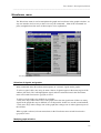
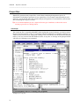
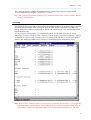
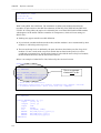
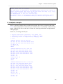
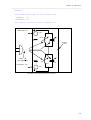
Appendix A
___________________________________________________________________________________
Format of the configuration file
At the beginning of the configuration file, general information must be given.
his2test samples all signals with a period introduced with the .PERIOD directive. This is the
strobing period. The .PERIOD directive must appear, it is not optional.
Syntax:
.PERIOD period_value
A default offset may be specified with the .DEFAULT_OFFSET keyword. This is the offset for
the strobing process. The .DEFAULT_OFFSET directive is optional. If no default offset is
specified, the default offset is zero. With a default offset specified, all signals in the .his file are
strobed at times: DEFAULT_OFFSET+n*PERIOD, with n=0,1,2..., unless they have a different
offset assigned, which overides the default (see below).
Syntax:
.DEFAULT_OFFSET def_offset_value
The total number of signals to be converted is introduced with the .SIGNAL_COLUMNS
directive. This directive must be given, it is not optional.
Syntax:
.SIGNAL_COLUMNS number_of_signals
The format of lines in the output file may be parametrized with the optional
.SEQUENCE_FORMAT directive. This directive introduces a string which defines the format of a
line (sequence) in the .tst file. Three tokens may be used in the string description, which are
substituted by their respective values: 'nseq' is the index of the sequence, 'tseq' is the time stamp,
and 'list' is the list of the signal values. Other characters may be given in the format string.
For example:
.SEQUENCE_FORMAT = "Sequence# 'nseq', at time 'tseq', is: < 'list'
>"
will produce this kind of output:
...
Sequence# 2, at time 100, is <111 1101 1001>
Sequence# 3, at time 150, is <011 110x 1101>
...
The default value of the sequence format is:
.SEQUENCE_FORMAT = "'nseq' 'list'"
Once these general parameters are given, the signal description begins. his2test lets you select the
signals you want to extract and convert from the .his file. The input signals must be given within
the .INPUTS section, and the output signals within the .OUTPUTS section. The .INPUTS section
starts with the .INPUTS keyword and is terminated by a .ENDS keyword. The .OUTPUTS section
starts with the .OUTPUTS keyword and is terminated by a .ENDS keyword. The signals in the
.INPUTS section are listed first, then the signals in the .OUTPUTS section.
Note: except for bidirectional signals, signals in .INPUTS section and signals in .OUTPUTS
section are treated identically.
Each signal in its section is introduced with a line which starts with the NAME keyword. It will
correspond to a column in the output file. Additional optional parameters may be specified along
the line. The signal description must fit on a single line in the .cfg file.
Syntax: (although shown on two lines below, this has fo fit on a single line)
461
SMASH™ Reference manual
___________________________________________________________________________________
NAME=name [OFFSET=offset] [SIGNAL_WIDTH=n] [BIDIR=direction]
[CONTROL_POLARITY=convention] CONTROL_NAME=ctrl_sig_name]
The NAME keyword introduces the name of the signal (which must be found in the .his file of
course).
The OFFSET keyword introduces a specific offset for the signal, which overides the default offset.
The SIGNAL_WIDTH keyword introduces the number of bitys of the signal, in case the signal is a
bus.
For example:
NAME = TRE
SIGNAL_WIDTH=4
means that TRE[0], TRE[1], TRE[2], and TRE[3] must be converted.
Specifying:
NAME
NAME
NAME
NAME
=
=
=
=
TRE[0]
TRE[1]
TRE[2]
TRE[3]
is equivalent.
The BIDIR keyword is used to indicate that this signal is a bidirectional signal (BIDIR=1). The
CONTROL_POLARITY keyword indicates the convention to use for this bidirectional signal, and
the CONTROL_NAME indicates the name of the signal to use for controlling the bidirectional
signal.
For a bidirectional signal, the CONTROL_NAME signal and the CONTROL_POLARITY
specifications control the direction of the signal. CONTROL_NAME introduces the name of a
control signal (a signal stored in the .his file, but which will not appear in the .tst file. Typically
this control signal is the command of the bidirectional driver for the birectional signal). This
control signal indicates if the bidirectional signal is an input or an output. The
CONTROL_POLARITY may be set to 0 or 1. If set to 0, the signal is considered as an input if the
control signal is 1, and as an output if the control signal is 0. If set to 1, the signal is considered as
an input if the control signal is 0, and as an output if the control signal is 1.
Example:
NAME=XINOUT BIDIR=1 CONTROL=0 CONTROL_NAME=OUTENB
To force an empty column in the .tst file, use lines containing the # character to separate groups of
signals.
Input signals will appear with three possible values, namely 0, 1 or z.
Output signals will appear with three possible values, namely 0, 1 or x.
462
Appendix A
___________________________________________________________________________________
Recapitulation of the .cfg syntax:
Note: the # lines in the sections are optional...
.PERIOD = period
.SIGNAL_COLUMNS = nb_of_signals
[.DEFAULT_OFFSET = default_offset]
[.SEQUENCE_FORMAT = "format_string"]
.INPUTS
#
NAME=name [OFFSET=offset]
CONTROL_NAME=ctrl_name]
#
NAME=name [OFFSET=offset]
CONTROL_NAME=ctrl_name]
NAME=name [OFFSET=offset]
CONTROL_NAME=ctrl_name]
NAME=name [OFFSET=offset]
CONTROL_NAME=ctrl_name]
#
.ENDS
[SIGNAL_WIDTH=n] [BIDIR=1 CONTROL=0|1
[SIGNAL_WIDTH=n] [BIDIR=1 CONTROL=0|1
[SIGNAL_WIDTH=n] [BIDIR=1 CONTROL=0|1
[SIGNAL_WIDTH=n] [BIDIR=1 CONTROL=0|1
.OUTPUTS
#
NAME=name [OFFSET=offset] [SIGNAL_WIDTH=n] [BIDIR=1 CONTROL=0|1
CONTROL_NAME=ctrl_name]
#
NAME=name [OFFSET=offset] [SIGNAL_WIDTH=n] [BIDIR=1 CONTROL=0|1
CONTROL_NAME=ctrl_name]
NAME=name [OFFSET=offset] [SIGNAL_WIDTH=n] [BIDIR=1 CONTROL=0|1
CONTROL_NAME=ctrl_name]
#
NAME=name [OFFSET=offset] [SIGNAL_WIDTH=n] [BIDIR=1
CONTROL=convention CONTROL_NAME=ctrl_name]
NAME=name [OFFSET=offset] [SIGNAL_WIDTH=n] [BIDIR=1
CONTROL=convention CONTROL_NAME=ctrl_name]
#
.ENDS
463
SMASH™ Reference manual
___________________________________________________________________________________
Example of a configuration file:
.DEFAULT_OFFSET = 20
.PERIOD = 100
.SIGNAL_COLUMNS = 9
.SEQUENCE_FORMAT = "Seq# 'nseq' at time: 'tseq' is: " 'list' ""
.INPUTS
#
NAME = OSC OFFSET = 30
#
NAME = Q3 BIDIR = 1 CONTROL_POLARITY = 0 CONTROL_NAME = CLK
NAME = Q3 BIDIR = 1 CONTROL_POLARITY = 1 CONTROL_NAME = CLK
#
NAME = CLR
NAME = CLEAR
#
.ENDS
.OUTPUTS
#
NAME = Q2
NAME = Q1
NAME = Q0
#
NAME = AOPOUT
#
.ENDS
Output generated by this configuration file:
Seq#
Seq#
Seq#
Seq#
Seq#
Seq#
Seq#
Seq#
Seq#
Seq#
Seq#
Seq#
Seq#
Seq#
Seq#
Seq#
Seq#
Seq#
Seq#
Seq#
Seq#
Seq#
Seq#
Seq#
Seq#
Seq#
464
0
1
2
3
4
5
6
7
8
9
10
11
12
13
14
15
16
17
18
19
20
21
22
23
24
25
at
at
at
at
at
at
at
at
at
at
at
at
at
at
at
at
at
at
at
at
at
at
at
at
at
at
time:
time:
time:
time:
time:
time:
time:
time:
time:
time:
time:
time:
time:
time:
time:
time:
time:
time:
time:
time:
time:
time:
time:
time:
time:
time:
0
100
200
300
400
500
600
700
800
900
1000
1100
1200
1300
1400
1500
1600
1700
1800
1900
2000
2100
2200
2300
2400
2500
is:
is:
is:
is:
is:
is:
is:
is:
is:
is:
is:
is:
is:
is:
is:
is:
is:
is:
is:
is:
is:
is:
is:
is:
is:
is:
"
"
"
"
"
"
"
"
"
"
"
"
"
"
"
"
"
"
"
"
"
"
"
"
"
"
0
0
1
1
1
0
0
0
0
0
0
0
1
1
1
0
0
0
0
0
0
0
1
1
1
0
z0
z0
z0
z0
z0
z0
z0
z0
z0
z0
z0
z0
z0
z0
z0
z0
z0
z0
z0
z0
z0
z0
0z
0z
z0
z0
11
11
11
11
11
11
11
11
11
11
11
11
11
11
11
11
11
11
11
11
11
11
10
10
10
10
000
000
000
000
000
000
000
000
000
000
000
000
000
000
000
000
000
000
000
000
000
000
000
000
000
000
1
1
1
1
1
1
1
1
1
1
1
1
1
1
1
1
1
1
1
1
1
1
1
1
1
1
"
"
"
"
"
"
"
"
"
"
"
"
"
"
"
"
"
"
"
"
"
"
"
"
"
"
Appendix B
___________________________________________________________________________________
Appendix B - Cross-probing with DesignWorks
Cross-probing
with DesignWorks
B
Overview
SMASH™ and DesignWorks for Windows (from Capilano Computing) can
communicate through DDE calls. Basic cross-probing is thus implemented between
SMASH™ graphic simulation windows, and DesignWorks schematics. Which means
that you can “probe” a signal or component directly in the schematic, and have the
voltage or current displayed in the SMASH™ screen.
465
SMASH™ Reference manual
___________________________________________________________________________________
SMASH™ and DesignWorks v3.1.1 for Windows can now communicate through DDE calls.
Basic cross-probing is thus implemented between SMASH™ graphic simulation windows, and
DesignWorks schematics. Which means that you can “probe” a signal or component directly in the
schematic, and have the voltage or current displayed in the SMASH™ screen.
To use this feature, you need SMASH™, DesignWorks for Windows, and the DDE.MDA file
from Capilano Computing. This file must be copied in the \tools directory of DesignWorks. Please
contact Dolphin or Capilano to get this file. For SMASH™ to connect with DesignWorks, you will
need to add a section named [CrossProbing] in the smash.ini file and a “DesignWorks =
yes” entry inside this section.
When using this cross-probing feature, always start DesignWorks first, then SMASH™. Load the
schematic with the Open Design... comand in DesignWorks. Load the circuit with the Load
Circuit... command in SMASH™. Simulate (for example: Analysis/Transient>Run). Display the
DesignWorks window and the SMASH™ window side-by-side. In SMASH™, bring the
simulation window to the front. Now click nets and components in the schematic... If the probed
signals were saved during the simulation, they are added in the simulation window.
The easiest way to work is to add the .LPRINT and .LPRINTALL directives in the pattern file, so
that ALL waveforms are saved during the simulation, and you can thus probe any signal you want.
If a signal is an interface signal, both the analog and the digital waveform are displayed when you
probe it.
Several options are available to control the cross-probing mechanism. In the smash.ini file the
[CrossProbing] section may contain the following entries (defaults are underlined).
DesignWorks = yes|no
DesignWorks_Receive = yes|no
DesignWorks_Single = yes|no
The DesignWorks entry is used to enable/disable the connection with DesignWorks. It is only
taken into account at SMASH™ start time.
The DesignWorks_Receive entry may be used to stop/resart the processing of the probes
which SMASH™ receives from DesignWorks. This entry is processed at each received probe.
Notice that you can also control the sending/receiving process in the “DesignWorks/Tools/DDE
The DesignWorks_Single entry is used to select the way a probed signal is added in the
SMASH™ window. If set to no (the default), the probed signal is simply added with the other
waveforms. If set to yes, the probed signal is added and displayed in “single” mode (as if you
would select the View this only command in SMASH™ to isolate it). In all cases, signals are
normally not added twice (if you probe a signal which is already in the displayed waveforms, it is
not added again).
You may probe nets, in which case either the voltage on the net or the logic value is added in the
waveforms, and you may also probe analog components (resistor, inductor, capacitor, bipolar or
MOS transistor, diodes and JFETS) to get the current(s) through the component.
466
Appendix C
___________________________________________________________________________________
Appendix C - Backannotation of SCS schematic
Backannotation of
SCS schematics
C
Overview
Backannotation of SCS schematics with operating point information is possible. It is
mainly suited for analog design. It is possible to backannotate a schematic with node
voltages, currents in resistors, transistors, voltage/current sources, and also some of the
small signal parameters for MOS, BJT, diodes and JFET devices. The backannotation
mechanism operates on the hierarchical view of the schematic (.tre), so it is possible to
backannotate hierarchical designs. Of course only SCS users are potentially interested in
this feature, and if you do not know what SCS is, you can safely skip this appendix...
467
SMASH™ Reference manual
___________________________________________________________________________________
It is recommended that you understand the SCS attribute concept to use the backannotation feature.
If you do not, we suggest that you read the SCS documentation before you proceed.
It is possible to backannotate a schematic with node voltages, currents in resistors, transistors,
voltage/current sources, and also some of the small signal parameters for MOS, BJT, diodes and
JFET devices. The backannotation mechanism operates on the hierarchical view of the schematic
(.tre), so it is possible to backannotate hierarchical designs. At the same time a .op file is generated
(Operating point analysis), SMASH™ generates an additional output file, with .atr extension. This
file is formatted to allow backannotation in the SCS schematic which was used to create the netlist
(.nsx). To use this feature, you will need to define additional symbol attributes in your ecs.ini file,
which will be dedicated to the backannotation process. These attributes may be defined with an
associated window number, so that you can choose to display the attribute value aside the
symbol/component. To understand the way it works, we suggest that you edit the sample SCS
symbols (.SYM files) in the .../news/backann directory. Associating a window to the
backannotation attributes is not mandatory. It is necessary if you want an attribute to appear in the
backannotated schematic. But in any case (except if you disable it, see below), the backannotated
schematic will contain the attribute value; if no window was associated to it, you can still get and
read its value with the Misc/Query command in SCS. The attribute values, as set by SMASH™ in
the .atr file, are loaded back into the schematic with the “Backannotate” command in SCS.
To trigger the creation of this attribute file, include a section named [ecsbackop] in the
smash.ini file, and add an “write_atr_file = yes” entry inside this section.
Here is an example of how to define these attributes in the ecs.ini file. Note that the name of the
attributes must be thoroughly respected, whereas their numbers are indifferent (simply choose
unused attribute numbers). The numbers used for the associated windows do not matter (simply
choose unused numbers). In the example below smash_opcurrent attribute is assigned number
154, and window number 14.
[SymbolAttributes]
...
smash_opv1
150,10
smash_opv2
151,11
smash_opv3
152,12
smash_opv4
153,13
smash_opcurrent 154,14
smash_oppower
155,15
smash_opregion
156,16
smash_opic
157,17
smash_opib
158,18
smash_opie
159,19
smash_opvth
160,20
smash_opvdsat
161,21
smash_opgm
162,22
smash_opgds
163,23
...
For each type of component (resistor, voltage source, MOS, etc.), only some of these attributes are
relevant. For example the resistor devices will only use smash_opv1, smash_opv2,
smash_opcurrent and smash_oppower attributes.
Some attributes are shared by several devices. For example the smash_opv1 and smash_opv2
attributes are used by all devices.
For each type of device, you may choose to exclude some of the attributes from the backannotation
process, by specifying an entry in the [ecsbackop] section in the smash.ini file, which will
prevent SMASH™ from writing these undesired attributes in the .atr file. The [ecsbackop]
section of smash.ini is a new one for SMASH™.
468
Appendix C
___________________________________________________________________________________
For example, imagine you do not care about the power dissipated in the resistor devices. There is
no need to backannotate this in the schematic. So you will enter show_res_p = no in the
[ecsbackop] section of smash.ini, like this:
[ecsbackop]
write_atr_file = yes
show_res_p = no
Now, for each supported device, the tables below will list the relevant attributes (those which are
backannotated by default), and how to disable them.
Resistors
Relevant attributes:
smash_opv1
smash_opv2
smash_opcurrent
smash_oppower
Content of attribute:
voltage on first pin
voltage on second pin
current in resistor
dissipated power
How to disable it:
show_res_voltages = no
show_res_i = no
show_res_p = no
Capacitors
Relevant attributes:
smash_opv1
smash_opv2
Content of attribute:
How to disable it:
voltage on first pin show_cap_voltages = no
voltage on second pin show_cap_voltages = no
Inductors
Relevant attributes:
smash_opv1
smash_opv2
Content of attribute:
voltage on first pin
voltage on second pin
How to disable it:
show_self_voltages = no
Voltage sources:
Relevant attributes:
smash_opv1
smash_opv2
smash_opcurrent
smash_oppower
Content of attribute:
voltage on + pin
voltage on - pin
current in source
dissipated power
How to disable it:
show_vsource_voltages = no
show_vsource_i = no
show_vsource_p = no
Content of attribute:
voltage on + pin
voltage on - pin
current in source
dissipated power
How to disable it:
show_isource_voltages = no
show_isource_i = no
show_isource_p = no
Current sources:
Relevant attributes:
smash_opv1
smash_opv2
smash_opcurrent
smash_oppower
Bipolar transistors:
Relevant attributes:
smash_opv1
smash_opv2
smash_opv3
Content of attribute:
How to disable it:
voltage on (internal) collector pin
show_bjt_voltages = no
voltage on (internal) base pin
show_bjt_voltages = no
voltage on (internal) emitter pin
469
SMASH™ Reference manual
___________________________________________________________________________________
smash_opic
smash_opib
smash_opie
Ic current
Ib current
Ie current
show_bjt_voltages = no
show_bjt_ic = no
show_bjt_ib = no
show_bjt_ie = no
MOS transistors:
Relevant attributes:
smash_opv1
smash_opv2
smash_opv3
smash_opv4
smash_opcurrent
smash_opvdsat
smash_opvth
smash_opgds
smash_opgm
smash_opregion
Content of attribute:
voltage on drain pin
voltage on gate pin
voltage on source pin
voltage on bulk pin
Ids current
saturation voltage
threshold voltage
D/S conductance (gds)
transconductance (gm)
LIN, SAT, SUB, OFF
How to disable it:
show_mos_voltages = no
show_mos_ids = no
show_mos_vdsat = no
show_mos_vth = no
show_mos_gds = no
show_mos_gm = no
show_mos_region = no
Content of attribute:
voltage on anode pin
How to disable it:
show_diode_voltages =
voltage on cathode pin
show_diode_voltages =
diode current
show_diode_i = no
Content of attribute:
voltage on drain pin
voltage on gate pin
voltage on source pin
Ids current
How to disable it:
show_jfet_voltages = no
show_jfet_i = no
Diodes:
Relevant attributes:
smash_opv1
no
smash_opv2
no
smash_opcurrent
JFET transistors:
Relevant attributes:
smash_opv1
smash_opv2
smash_opv3
smash_opcurrent
Backannotation of node voltages
If you want to backannotate the node voltages as computed by SMASH™ during the Operating
point analysis, you may use a special SCS symbol, which looks like a little hook you attach on the
nodes you want to be backannotated. This symbol is actually a capacitor with its pins wired to each
other. They will appear as capacitors in the netlist, but they will have absolutely no electrical
effect, as they are shorted. This special hook symbol (which you may redraw as you like, with the
symbol editor), has its smash_opv1 attribute in a window. When the capacitors are
backannotated, the voltages on the capacitor pins are written to the smash_opv1 and
smash_opv2 attribute. So if the smash_opv1 window is made visible in the hook symbol, the
node voltage appears in this window. See the examples in the .../news/backann directory.
470
Appendix C
___________________________________________________________________________________
« Hook » symbol for node voltages backannotation:
Relevant attributes:
smash_opv1
smash_opv2
Content of attribute:
voltage on first pin
voltage on second pin
How to disable it:
N/A
N/A
Instructions for using the backannotation feature (tutorial)
The .../news/backann directory contains sample SCS and SMASH™ files to illustrate the
backannotation process.
• Verify that you ecs.ini file contains the definitions for the backannotation attributes, in the
[SymbolAttributes] section.
• First, you need to create your schematic, using primitive symbols which contain the
desired backannotation attributes and windows. For example see the NPN.SYM symbol (open it
with Edit Symbol and see how it is designed).
• Then, if you want node voltages to appear in the schematic, you must add some “hooks” in
the schematic. When you attach such a “hook” symbol, no value is displayed. The node voltage
value will appear when you backannotate the schematic. For example open the retrobip.sch
schematic (Edit schematic) and locate the “hooks” which were attached to different nets. In this
example the “hook” symbol is NODEHOOK.SYM. You may use any name yo want for your own
usage.
• Once the schematic is ok, you need to build the hierarchy with the Navigate Hierarchy
netlist, run SMASH™ and simulate the design (at least, run
an Operating point analysis). Try it with the retrobip.sch schematic in the .../news/backann
directory. If you are not familiar with this procedure, well, hum..., read chapter 15 in the
SMASH™ manual, play with the tutorial, then continue...
• Ok, now we have a retrobip.atr file with the backannotation information (you may open it
file). Switch back to the navigator window, and activate the
File/Backannotate command. Enter retrobip.atr at the prompt, then click OK. You will probably
get error messages. Simply close the error messages window and ignore them. Now you see the
node voltages, and some of the small signal parameters of the transistors.
Note: sometimes, SCS does not refresh all symbol attributes properly, when the File/Backannotate
command is run. To be sure everything is properly refresed, you may have to activate the
View/Redraw command immediately after the File/Backannotate one.
471
SMASH™ Reference manual
___________________________________________________________________________________
472
Appendix D
___________________________________________________________________________________
Appendix D - Batch mode under Unix
Batch mode
under Unix
D
Overview
On Unix systems, SMASH™ can be used in batch mode, from a console, without calling
the X-window interface. To do so you need to provide some options which trigger the
batch mode and specify the differents analyses. It allows you to run long simulation(s)
using a script, possibly at night. Batch mode simulations generate result files which can
be later analyzed with the interactive version of SMASH™.
473
SMASH™ Reference manual
___________________________________________________________________________________
How to use SMASH™ in batch mode
The batch mode of SMASH™ is launched with the -b option following the command "SMASH" at
the prompt shell. If you just used the -b option (i.e. SMASH -b) you will see the following
message that displays an help about the differents options.
Warning: if you work on a console and you forget to specify the “b” option, you might run the
graphical version of SMASH™... on a networked X-window display...
Use this help to know the exactly format of the command line and the signification of each option.
host_prompt> SMASH -b
------------------------------------------------------------ SMASH 3.0 - Copyright (c) by Dolphin Integration, 1993. -----------------------------------------------------------There are some errors in your command line,
use the following format to run SMASH in batch mode.
Where [] indicates an optional character
and | a choice between options
Format: SMASH -b[a|d|n|o|p|t|v][s|m] simulation_file
or
Format: SMASH -b[A|D] module_file
-----------------------------------------------------------b : batch mode
a : small signal analysis (AC)
d : DC transfert analysis
n : noise analysis
o : operating point analysis
t : transient analysis
v : verify circuit
s : sweep mode analysis
m : monte carlo analysis
simulation_file : file name without its extension
-----------------------------------------------------------A : compile analog module
D : compile digital module
module_file : file name with its extension
-----------------------------------------------------------There are two formats: one for simulation, the other for behavioral module compilation (if you are
licensed to).
The first format is used to run a simulation on the circuit named simulation_file. To do this,
you need two files: simulation_file.nsx and simulation_file.pat (See the User
Manual) and it works as if you had used menu commands in the graphical version of SMASH™.
Example:
if you want to run transient simulation on circuit named
filters.nsx/filters.pat, enterthe following command at the prompt:
host_prompt> SMASH -bt filters
where “b” triggers the batch mode and “t” indicates a transient
simulation.
If you want to run a transient sweep simulation, just add “s”:
474
Appendix D
___________________________________________________________________________________
host_prompt> SMASH -bts filters
These commands load the circuit, check if it is correct, run operating point simulation, and then
run a transient simulation. If there are some errors in these different phases, SMASH™ will stop
and report the error. You need to edit the circuit.rpt file to verify if there are some warnings.
The second format is used to compile a behavioral module. In this format, you have to write the
module name with its extension (usually “.txt”). Use the “A” option to compile an analog
module or “D” option to compile a digital module.
Example:
host_prompt> SMASH -bA za_aop.txt
It works as if you had used the menu item Load > Compile analog module in the graphical version
of SMASH™. The result of compilation is displayed on your screen.
How to visualize the results of simulation
When launching SMASH™ in batch mode, it will create some results files in binary format (.tmf,
.amf ...) and ASCII files if you use .CREATEHISFILE .CREATEICDFILE directives. To visualize
the binary files, you have to use the graphical version of SMASH™, load the circuit (Load
Circuit), bring the desired simulation window to front (Windows Transient for ex.) and activate the
Load Waveform menu item.(See the User Manual: Load menu, Waveform item)
475
SMASH™ Reference manual
___________________________________________________________________________________
476
Appendix E
___________________________________________________________________________________
Appendix E - Cookbook
Cookbook
E
Overview
This « cookbook » appendix contains a number of hints and answers to frequent
questions. If, during your work with SMASH™, you happen to find out new tips in this
style, we would appreciate you fill and send the suggestion form back to us, so that we
can improve things. The suggestion form is in appendix I.
477
SMASH™ Reference manual
___________________________________________________________________________________
Tip for MS-Windows users
It is highly recommended to frequently use the CHKDSK command on your PC. If the file system
is corrupted, the CHKDSK /F command will try to fix it. SMASH™ can give rather strange
results if you operate on a corrupted file system. The nature of problems occuring when the file
system is damaged is highly variable. You may get a system “hang”, or simply corrupted output
files.
Particularly, if you have a crash when running SMASH™, quit Windows, and do a CHKDSK /F,
as crashes of Windows-based programs often damage the file system. If you CHKDSK your disks
regularly, you will avoid many problems.
Tip for Unix/X-window users
DO NOT close the dialog boxes with the close box (the little icon in the corner of the dialog
window). Use either the Ok or Cancel button.
Redraw is slow (Unix)
If you manipulate large files, redraw may be slow. Close all windows you do not use. Interrupting
the redrawing of a simulation window is possible, either partially by clicking the rightmost mouse
button, or completely by typing ESC. If the click right does not seem to have any effect, try
clicking with the mouse in the main SMASH window (the wide one on top of the screen).
Color of the grid switches at random (Unix only)
This happens sometimes, apparently depending on the X-window driver releases. It does not hurt,
simply it is not pleasant. To reset things, select the Full Fit item in the Waveforms menu.
I can not get a .op
Consult the manual, chapter 9 - Directives, .OP directive.
If you use the BSIM model, set parameters NO, NB and ND to 0.0.
If possible, use simpler models for the transistors, try to get a circuit.op file with these simple
models, then take the original again and use the “Start off with .op file” option or
.USEOP directive.
If you have tried everything you can think of, and it does not work, try to reduce the circuit as
much as you can, and send it to the address on the last page of the manual.
I get a “Bad news! time step etc.” message in transient analysis
Check your circuit, its topology, the values of the components, and the model parameters.
Remove all optional directives from your pattern file, and verify that you still get the problem
when all is “by default”.
Try to use the .CAPAMIN directive to add a small capacitance to ground on all analog nodes. This
helps convergence in transient analysis.
Try to reduce the Minimum time step in the Transient > Parameters dialog (see .H directive).
Try to reduce the Nominal time step in this same dialog.
Try to have less sharp edges in your voltage sources (PULSE and PWL).
478
Appendix E
___________________________________________________________________________________
Try to increase the “Current accuracy” in the Transient > Parameters dialog. Change it from 1e-9
(the default) to 1e-8 etc.
If you have interface nodes (mixed mode simulation), try to increase the .LRISEDUAL parameter
or the TPLH, TPHL, TPZ and TPNZ of your interface models, so that the transitions on these
nodes are less sharp.
With the EKV model, use NQS=0
My transient simulation takes ages
Remove all optional directives from your pattern file, and verify that you still get the problem
when all is “by default”.
Check that the number of points you require is adequate (this is the ratio duration/drawstep in the
.TRAN directive). If you have “.TRAN 1p 1m”, you are asking for 1.000.000.000 points. No doubt
this will take a while...
Check the Internal time steps you are using. DO NOT use an infinitesimal nominal time step. Try
to allow a larger maximum time step.
Try to increase the “Current accuracy” in the Transient > Parameters dialog.
If you are a Unix user, consider using the batch version (see Batch mode appendix).
Consider using the .EXCLUSIVE directive. You will loose interactivity, but this will speed up the
simulation.
If you do not need it, avoid using the .PRINTALL and .LPRINTALL directives, and select the
signals you want to save with .PRINT and .LPRINT directives.
On Unix machines, avoid (if possible) busses in .TRACE directive.
Consider displaying only the necessary waveforms, not a whole bunch of 32-bits busses you do not
even look at...
If possible, add a /ZS=1 postfix on the output nodes in analog behavioral modules. This reduces
the number of unknowns. See chapter 13.
If applicable (see the discussion in the manual), consider using the .RELAX directive and
relaxation mode.
Consider using equation-defined sources to replace analog functions.
Consider using analog behavioral modelling. See chapter 13.
When doing several successive zooms, the scalings get unusable (all values identical)
Use the .DIGITS directive to increase the number of significant digits of displayed numbers.
In the dialogs, the decimals of numeric values are truncated
Use the .DIGITS directive to increase the number of significant digits of displayed numbers.
I get a “Too many analog sources” error message when loading circuit
479
SMASH™ Reference manual
___________________________________________________________________________________
Use the .MAXSOURCES directive to increase the maximum number of voltage and current
sources.
I get t_xx files in the root directory (PC only)
You can delete them. To have them created in a temporary directory, create a C:\TMP directory,
and define the TMP environment variable as C:\TMP, with a SET command in the autoexec.bat
file:
SET TMP=C:\TMP
From time to time, delete t_xx files which may be left in the C:\TMP
directory.
I get ??aa???? files in the /usr/tmp directory (Unix only)
You can delete them. Consider installing an automatic clean-up of this directory in your .login file.
The Small signal menu stays greyed
Add AC 1 0 at the end of the voltage source definition you consider as the input. See chapter
6.
I get empty graphs or crashes when the number of traces gets large (PC)
Enter the FILES=50 command in the config.sys file.
How can I create a digital clock with “holes”, without using a WAVEFORM
You have to connect two .CLK “gates” on the same digital node.
Example:
.CLK CLOCK 0 D0 10 D1 .REP 20
.CLK CLOCK 0 Z0 1000 D0 1350 Z0
From 0 to 1000, you will have a normal clock, then from 1000 to 1350, it will be zero, and start
again as a clock at time 1350.
How can I build .lib files from individual files
On the PC, use the copy command
Example:
copy *.ckt allckt.lib
This will make an allckt.lib file with all files with extension .ckt
Example:
copy AOP1.ckt+AOP2.ckt allaop.lib
This will make an allaop.lib with the two .ckt files
On Unix, use the cat command
Example:
cat *.v > my_v_lib.lib
This will make a my_v_lib.lib file with all files with extension .v
I can not select a signal during a simulation
If it is a big simulation, interactivity is reduced, so be patient...
If really you can not select anything, maybe it is because you are in zoom or scroll mode. In these
modes, the cursor’s shape is normally changed, but it is not if a simulation is running. To get out of
480
Appendix E
___________________________________________________________________________________
the zoom mode, click the right most button of the mouse or hit the ESC key. then try to select your
signal.
481
SMASH™ Reference manual
___________________________________________________________________________________
482
Appendix F
___________________________________________________________________________________
Appendix F - Error messages
Error messages
F
Overview
This appendix lists the error messages you may encounter. The messages are sorted
alphabetically. A short explanation is given for certain messages, as well as the chapter
to consult for more details.
483
SMASH™ Reference manual
___________________________________________________________________________________
Error message
What it means, and what do do...
A digital driver (gate output or
stimulus) cannot be shorted with a
voltage source...
A numeric value was expected
here...
Your circuit contains a forbidden configuration. A digital gate drives a
voltage source. This is a short-circuit which is not allowed. See chapter
12.
The parser expected a valid numeric value. A numeric value can be a
litteral value (such as 1.34, 1K, 350U) or an expression using
parameters (from .param directives, or subcircuit parameters).
Expressions must be enclosed within single quote characters :
.param p1 = 1
.param p2 = 5
.param p3 = ‘p1*p2’
for example.
The instanciation does not match the definition. You must verify that the
instanciation has the same number of inputs, of outputs and parameters.
Also the output types (voltage or current with a /I specification) must
match. See chapter 13.
The .IC directive syntax is wrong. Correct syntax is :
.IC V(NODE) = value
where NODE is an existing analog node, and value a valid numerical
value.
SMASH tried to parse an interface device (an instance whose first
character is N) and an error occured. The correct syntax is :
NXXX MIXEDNODE VSSNODE VDDNODE MODELNAME
where NXXX is the instance name, MIXEDNODE is an interface (mixed
analog/digital) node, VDDNODE is the positive power supply connection,
and VSSNODE the negative one. Normally VDDNODE and VSSNODE
should be connected to independant voltage sources. MODELNAME must
be the name of an interface device model. See chapter 12 for further
details.
SMASH tried to parse a conditional equation-defined source, and found
an incorrect operator symbol in the IF clause. In the IF clause, only the
indicated operators are allowed.
Indicates an error in a formula expression (equation-defined source or
.param statement).
The BEHAVIOR keyword must appear in your module source code. It
must be the sole word of the line where it appears.
SMASH detected an error while parsing an instance of a behavioral
module. The syntax for such an instanciation is (assuming the case of a
module with two inputs, two voltage ouputs and two parameters):
Analog behavioral module call does
not match prototype...
Bad .IC directive...
Bad interface device instance...
Bad operator in IF clause (should
be one of: <, <=, >, >=,
==,...=)...
Badly formed formula tree.
BEHAVIOR keyword not found...
Behavioral module call is wrong...
Zxxx IN( IN1 IN2 ) OUT( OUT1 OUT2 ) PAR( P1 P2 ) ZMOD
BIN, DEC or HEX keyword is
expected...
Binary string length is wrong...
Binary value is wrong...
484
where Zxxx is the instance name, INi the inputs, OUTi the outputs, Pi
the parameters (numerical values). Notice that the parser does not forgive
much for these instances. ALL spaces in the line above MUST be
present. Also you must write :
IN( IN1 IN2 )
not :
IN(IN1 IN2)
Same thing for OUT( and PAR(.
ZMOD must be the name of an existing, compiled, behavioral module (file
ZMOD.AMD must exist and it must be referenced as a library file (.lib
c :\library\zmod.amd) for example.
When describing busses in a WAVEFORM clause, the expected radix is
binary (keyword BIN), decimal (keyword DEC, or hexadecimal (keyword
HEX). If no such keyword is detected, you will get this error.
The length of the binary string (a character string composed of O, 1, X
and Z symbols) does not match the width of the bus. For example
writing :
+100 IN[7 :0] = BIN 000011110
is an error because IN is 8 bits wide and the string is 9 characters long.
The binary string specified as the value of a bus in a WAVEFORM clause
is incorrect. The most probable reason is that it contains unauthorized
characters/symbols. Use only 0, 1, X and Z.
Appendix F
___________________________________________________________________________________
Bipolar transistor instance is
wrong...
Bipolar transistor model
redefinition. Check .MODEL
statements...
Bus index is wrong...
Bus indexing is wrong...
Bus specification is expected...
Bus specification is wrong...
Instance (X-statement) and
definition (.SUBCKT statement) do
not match (not the same number of
connections)...
Capacitor instance is wrong...
Clock specification is wrong...
Closing ')' expected in strbin()
function call...
Closing parenthesis expected to
indicate end of IN( section...
Closing parenthesis expected to
indicate end of OUT( section...
Closing parenthesis expected to
indicate end of PAR( section...
Closing parenthesis expected to
indicate end of STRPAR( section...
Command is wrong (.AC)...
Command is wrong (.DC)...
Command is wrong (.EPS)...
Command is wrong (.H)...
Command is wrong (.TEMP)...
An error was detected while parsing a bipolar transistor instance. Correct
syntax is :
Qxxx C B E MODEL [area]
or
Qxxx C B E [S] MODEL [area]
The area factor is always optional, and it must be the last word on the
line. The substrate node must be enclosed in square brackets if it is
composed of letters.
A bipolar transistor model (.MODEL statement) is defined more than once
it the same scope, which is not allowed. Search for a double definition of
the .MODEL statement which defines the model parameters.
The passed value could not be interpreted as a valid numeric integer
value.
This error occurs if you specify a bus whose start and end indexes are
identical, such as IN[3:3]
A bus was expected. A bus is built with a base name and a range
specification (two integer values separated by a colon, enclosed in square
brackets). Examples :
A[7:0]
B[31:16]
This message occurs if the colon was not detected.
A bus specification could not be deciphered. The construction of a bus is
described above.
A subcircuit instance was found, where the number of connections was
incorrect. If you define a subcircuit with three connections, instances of
this subcircuit MUST have three connections exactly. Double check the
X-statement (instance) and the corresponding .SUCKT definition.
The possible syntax for a capacitor is one of the following :
Linear capacitor :
Cname n1 n2 val
or non-linear capacitor :
Cname n1 n2 POLY val vc1 vc2 vc3
The .CLK statement is wrong. See chapter 6 for a detailed description of
the syntax. Verify the values for the time values, and the symbols you are
using for the logic levels.
Indicates a simple parenthesis mismatch.
The closing parenthesis must be isolated (preceeded and followed by at
least one white space).
The closing parenthesis must be isolated (preceeded and followed by at
least one white space).
The closing parenthesis must be isolated (preceeded and followed by at
least one white space).
The closing parenthesis must be isolated (preceeded and followed by at
least one white space).
.AC directive defines the parameters for the AC (small signal) analysis.
The correct syntax is :
.AC DEC|LIN n fstart fstop
For example :
.AC DEC 10 100 100K
this will define an AC analysis with a log. Scale, with ten points per
decade, from 100Hz to 100kHz.
Hint : remove the .AC line from the .pat, reload and use the dialog instead
(Analysis>small signal>parameters...). It will edit the .AC line for you.
.DC defines the parameters for a DC transfer analysis. The correct syntax
is :
.DC VNAME vstart vstop vincrement
where VNAME is the name of an independant voltage source. VNAME
could be defined as :
VNAME IN GND DC 5.0
for example.
Vstart, vstop and vincrement define the limits for the analysis.
Hint : remove the .DC line from the .pat, reload and use the dialog instead
(Analysis>DC transfer>parameters...). It will edit the .DC line for you.
Use the Analysis>Transient>Parameters dialog.
Use the Analysis>Directives dialog.
485
SMASH™ Reference manual
___________________________________________________________________________________
Command is wrong (.TRAN)...
Compilation script failure. No
compiled version was created...
CUDG_WRITER: Bad index... (range
for a bus index is 0..31)
CUDG_WRITER: Bad name...
CUDG_WRITER: Duplicate names in
pins, parameters and signals...
CUDG_WRITER: Too many global
boolean variables...
CUDG_WRITER: Too many global double
variables...
CUDG_WRITER: Too many global
integer variables...
CUDG_WRITER: Too many internal
signals...
Current controlled sources must be
controlled by independant
sources...
Current source definition is
wrong...
Decimal value is wrong...
DECLARATIONS keyword not found...
Use the Analysis>Transient>Parameters dialog.
A problem occured while compiling a behavioral module. The command
file which actually activates the C compiler returned an error. Verify that
the DIRMODULES environment variable is defined and points to the right
directory. Verify that your C compiler is properly installed and that the
PATH, INCLUDE and LIB variables are properly set. See tutorials in
chapters 13 and 14, and/or tutorials you may find in the installation
directory.
Indexes for busses in a C-based module must be in the range 0 to 31.
The identifier is not accepted as a pin name.
You must use unique identifiers for the pins, parameters and signals that
you declare. Duplicate identifiers are forbidden.
Limit is 16.
Limit is 16.
Limit is 16.
Limit is 256.
Independant sources are defined as (for example) :
VIN INPUT 0 1.0
or
VIN INPUT 0 SIN 0.0 1.0 100K
They provide a voltage across their connections which is not controlled
by any other voltage or current source. Only this type of voltage source
may control a current controlled source.
Use the dialog to edit sources instead...
The decimal value specified as the bus value is incorrect.
DECLARATIONS is a keyword which is expected as the very first line in
a source file for a Z-style analog behavioral module. Double-check its
presence and exact spelling.
Digital behavioral module call does The module interface declaration does not match the call. You must pass
not match prototype...
the same number of connections and parameters if any.
Digital stimulus (defined with a
An interface node is a node which is connected to at least one analog
.CLK directive, or within a
element (such as a resistor, a diode etc.), and at least one digital element
WAVEFORM clause) can not drive
(a nand gate for example). Such a node has a double nature. You can
directly an interface node
view the voltage it carries, and also its logic level. A few configurations
(analog/digital node). Please
insert a digital buffer (buf gate) are forbidden for these nodes. The one described by the message is a
common one. If you want to drive an interface node with a clock (.CLK
between the stimulus and the
statement or WAVEFORM statement), you need to insert a digital buffer
interface node.
bewteen the digital stimulus node and the electrical interface node. See
chapter 12 for details about this configuration and the way to work
around.
Diode instance is wrong...
Syntax for a diode instance is :
Dxxx NA NC DMODEL [area]
where DMODEL must be the name of a diode model defined with a
.MODEL statement. Area is an optional area factor.
Diode model redefinition. Check
An other diode model with the same name was already defined within the
.MODEL statements...
same scope. Search for duplicate .MODEL statements which define the
same diode model name.
Directory for this file must have
This is a typical Unix problem when a directory is write-protected, and
write access...
SMASH needs to create a file. This happens if you install SMASH as
« root » and you attempt to run the examples in directories which are
root ». Either move the examples to a directory which you
own, or change (or have changed) the permissions for this directory.
Duplicate instance name... This
Instance names for devices must be unique. You cannot have two
instance name was already used by
resistors named R1. Having both :
an other device...
R1 A B 10K
and
R1 C D 100K
is illegal. Of course you may have several « local » R1 names, if
instanciated in different subcircuits. But within a common scope (in the
top-level or in the same subcircuit), all devices must have a unique name.
Duplicate module instance name...
See above.
486
Appendix F
___________________________________________________________________________________
ELSE keyword expected...
Equal sign (=) is missing...
The parser expects an equation-defined voltage or current source. Simple
sources introduce the expression with the VALUE keyword. Conditional
sources use the IF THEN ELSE construct. Examples :
E1 OUT 0 VALUE {2*V(IN)}
E2 OUT 0 IF {V(IN) > 0} THEN {5.0} ELSE {V(IN)}
SMASH expected an = sign. Examples :
WAVEFORM xxx
0 A = 1, B = 0 ;
100 A = 0 ;
FINISH
The analyzed expression is incorrect. Probably parenthesis are not
properly balanced, or a non-existing signal or function is referenced.
Double-check the expression and retry.
Error while building default
Internal consistency error. Please pass information to our technical
interface devices...
support.
Error while opening pattern file... The .pat file (or .cir) has been corrupted. Quit SMASH, verify the files
with an other editor. « scandisk » your hard disk for logical errors.
Error while saving pattern file... See above.
Error while saving temporary
System refused to create/write a temporary file. Verify the write
file...
permissions in the TMP directory. If ok, either the file system is
saturated, or the memory is saturated. Quit SMASH, reboot and retry. If
you still have problems, pass the problem to our technical support.
Expression expected.
Internal error in the expression parser. Please pass the problem to our
technical support.
Fatal memory error. See
This is a fatal error message... It is generated when a memory allocation
memerror.log file. Unable to
request can not be fullfilled by the operating system. A file
proceed...
« memerror.log » is generated. The context is displayed in this file. This
may give a hint about the cause of the problem. Immediately after the
message, the application quits. You may try to close as many applications
as possible, and retry. If you still have this message, and you suspect it is
not normal (if your circuit is huge, it may be normal, and in this case you
should simply install more RAM...), try to reboot the system. As a last
action, send the files to the technical support.
Hexadecimal value is wrong...
The hexadecimal value specified as the bus value is incorrect.
Hexadecimal values may contain 0..9 and A..F characters.
Hierarchical instance name would be See below.
too long...
Hierarchical name would be too
During the loading phase, SMASH builds internal data structures which
long...
represent the circuit. Particularly, hierarchy is expanded (flattened),
which generates hierarchical names for the instances and the nodes. The
full hierarchical names are limited to 64 characters. If you get this
message, try to reduce the length of the instance names, and the length of
the node names. Use XM instead of XMEMORY for example, and N1
instead of MYINTERNALNODENUMBER1.
IN( keyword expected...
SMASH tried to parse an instance of an analog behavioral model, and no
IN( keyword was found. The IN( keyword introduces the list of inputs
to the module.
Beware that SMASH expects to find exactly IN( not IN ( or IN {
etc. The list of inputs must be separated by one or more spaces and
terminated with an ISOLATED parenthesis. Example :
Error while analysing formula...
Z1 IN( CLK IN VSS VDD ) OUT( OUT/I ) PAR( 1.0 ) ZA_DFF
Index for ALLOCATE_MEMORY macro is
wrong ( should be in interval 0..
4)
Inductor instance is wrong...
would be correct.
Self explanatory. Use allowed index only.
Correct syntax for an inductor is :
Lxxx N1 N2 value
where Lxxx is the instance name, N1 and N2 are nodes, and value a
valid numeric value.
487
SMASH™ Reference manual
___________________________________________________________________________________
Instance name is too long...
During the loading phase, SMASH builds internal data structures which
represent the circuit. Particularly, hierarchy is expanded (flattened),
which generates hierarchical names for the instances and the nodes. The
full hierarchical names are limited to 64 characters. If you get this
message, try to reduce the length of the instance names, and the length of
the node names. Use XM instead of XMEMORY for example, and N1
instead of MYINTERNALNODENUMBER1.
Instance (X-statement) and
A subcircuit instance was found, where the number of connections was
definition (.SUBCKT statement) do
incorrect. If you define a subcircuit with three connections, instances of
not match (not the same number of
this subcircuit MUST have three connections exactly. Double check the
connections)...
X-statement (instance) and the corresponding .SUBCKT definition.
Instance/definition mismatch (not
A subcircuit instance was found, where the number of parameters was
the same number of parameters)...
incorrect. If you define a subcircuit with three parameters with the
backslash syntax, instances of this subcircuit MUST have three
parameters exactly. Double check the X-statement (instance) and the
corresponding .SUBCKT definition. See chapter 5 for the detailed syntax
of parametrized subcircuits.
Interface model redefinition...
An interface model with the same name was already defined. Model
definitions must be unique within their scope.
Interface node has more than one
An interface node may contain at most one explicit interface device (N
interface device connected...
devices, see chapter 12).
Interface nodes cannot be driven by Your circuit contains a forbidden configuration. An interface node can
more than one digital gate...
not be driven by several digital drivers. It may contain as many analog
connections as you want, but no wired logic is authorized on it. A single
digital driver (output of a digital gate) may drive the interface node.
Jfet model redefinition... Check
A junction FET transistor model with the same name was already
.MODEL statements...
defined. Model definitions must be unique within their scope.
Junction FET instance is wrong...
Syntax for a JFET instance is :
Jxxx D G S JMODEL
where JMODEL is the name of a JFET model defined with a .MODEL
statement.
K device: coupling factor must be
Self-explanatory.
in [0,1] interval.
K device: parameter is missing.
The coupling factor is missing. This must be the last item on the line.
K device: referenced L device is
You are referencing a non-existing inductor in a K statement/device.
unknown.
Double-check the name of the inductors.
LAPLACE device description is
An unexpected item is present in the instance. Refer to the syntax
wrong...
definition in chapter 3.
Library file: \filename/file
In a library file (.mdl, .ckt, .mac), the name of the file must match the
content\ mismatch...
name of the element. In a file named opamp.ckt you must define a
subcircuit whose typename is opamp. Nothing else is allowed. So open
the libary file, and verify that the typename (for a .ckt) or the name of the
model (for a .mdl) matches the name of the file.
Logic level specification is
See chapter 7.
wrong...
Lookup table instance: closing
See detailed syntax in chapter 3.
curly brace (}) expected...
Lookup table instance: construction See detailed syntax in chapter 3.
of the spline vector failed...
Lookup table instance: equal sign
See detailed syntax in chapter 3.
(=) expected...
Lookup table instance: even number See detailed syntax in chapter 3.
of values expected...
Lookup table instance: input
See detailed syntax in chapter 3.
expression V(N), V(N1, N2) or
I(VSRC) expected...
Lookup table instance: opening
See detailed syntax in chapter 3.
curly brace ({) expected...
Lookup table instance: TABLE,
See detailed syntax in chapter 3.
S_TABLE or N_TABLE keyword
expected...
Loop length is too large (max is
Reduce the number of transitions in the loop.
200 lines)...
488
Appendix F
___________________________________________________________________________________
Loop length value expected...
Macro call does not match
definition...
Macro is unknown...
Macro redefinition...
Maximum bus length is 32...
Missing BEHAVIOR: keyword...
Missing closing parenthesis for
expression.
Missing closing parenthesis for
function.
Missing data...
Missing END_MACRO keyword...
Missing identifier...
Missing information in formula
device description...
Missing parameters for LAPLACE
device description...
Model definition expected...
Model type is wrong...
Module could not be loaded...
Syntax for a loop definition inside a WAVEFORM clause is :
LOOP value
...
ENDLOOP
where value is an integer figuring the number of times the loop has to be
processed.
See chapter 8.
See chapter 8.
See chapter 8.
Self explanatory.
The BEHAVIOR keyword must appear in your module source code. It
must be the sole word of the line where it appears.
Self explanatory.
Self explanatory.
See chapter 8.
A behavioral module could not be loaded. Behavioral modules are
dynamic link libraries (DLLs on PC). Either the compiled version of the
module file was missing, or there is a version problem. For example, you
cannot use a 32-bit module with the 16-bit version of SMASH. If your
option allows you to recompile the module, then delete the .amd or .cba
or .dmd, recompile it, and retry. If you are using a sample module from
the sample library, then be sure you are pointing to the right version.
MOS transistor instance is wrong... The full syntax for a MOS transistor instance is :
Mname nd ng ns nb model W=w L=l [AD=ad] [AS=as]
+ [PD=pd] [PS=ps] [NRD=nrd] [NRS=nrs] [M=m]
Values for W and L are mandatory. Other parameters are optional. See chapter 3
for a detailed description of the syntax.
MOS transistor model redefinition.
Check .MODEL statements...
.SUBCKT definition without
corresponding .ENDS statement...
Node is unknown...
Node name is incorrect...
Node name was not acceptable...
Node numbers for ports are allowed
for subcircuits containing analog
primitives only. Use node names.
Non composable function.
Not enough memory left.
Number of bits is wrong (second
argument of strbin() call)...
Number of input connections:
mismatch...
Number of output connections:
mismatch...
A MOS transistor model (.MODEL statement) is defined more than once
in the same scope, which is not allowed. Search for a double definition of
the .MODEL statement which defines the model parameters.
A subcircuit definition was started with a .SUBCKT statement, but no
corresponding .ENDS was found. See chapter 5 for details about
subcircuit definitions.
The .HIST directive references an unknown node.
The name for the node contains characters which are not allowed as part
of a node name. Remove all « exotic » characters from the name.
Same as above.
This message occurs if you use numbers (such as 11, 45 or 104) instead
of names for subcircuit definitions. The general recommendation is :
USE NODE NAMES. This archaic habit is only partially supported
because it conflicts with Verilog-HDL syntax. Partial solutions exist
however : see the .PUREANALOG directive description in chapter 9.
Indicates an error in an expression. This is often related to missing or
extra parenthesis. Verify the structure of your expression. Start with a
simple one, and progressively build the final expression if necessary.
See strbin() function in chapter 8.
The number of inputs declared in the module source code, in the
DECLARATIONS section, does not match the number of connections
passed in the input list of the instanciation. These counts have to match
exactly.
The number of ouputs declared in the module source code, in the
DECLARATIONS section, does not match the number of connections
passed in the output list of the instanciation. These counts have to match
exactly.
489
SMASH™ Reference manual
___________________________________________________________________________________
Number of parameters: mismatch...
The number of parameters declared in the module source code, in the
DECLARATIONS section, does not match the number of connections
passed in the parameter list of the instanciation. These counts have to
match exactly.
Numerator degree must be lower than Self explanatory.
or equal to the denominator
degree...
Opening '(' expected in strbin()
strbin is a function. An opening parenthesis is expected.
function call...
OUT( keyword expected...
The OUT( keyword was not found. Notice that the parenthesis is part of
the keyword.
Output connections list is
The OUT( ) list of ouputs was not found. Notice that the opening
missing...
parenthesis in OUT( is part of the keyword.
Parameters not allowed...
Parenthesis expected...
Pin count mismatch (internal
Internal consistency error. Please pass information to the technical
consistency error)...
support.
Postfix is not valid (allowed
The postfix you are using for a numeric value is not supported. Allowed
postfixes are: F,N,U,M,K,MEG,T)
postfixes are : F, P, U, M, K, MEG, G, T, dB
Problem re-opening .rpt file after Internal error. Please contact the technical support.
Verilog preprocessing...
PWL-type source instance: first
See below.
time value must be zero (0)...
PWL-type source instance: time
The time values specified in a PWL source must be given in a strictly
values must verify: 0 <= t(i) <
increasing order. The first time value must be zero.
t(i+1)...
READBUS() call does not match
See function description in chapter 13.
prototype...
Relative time specification is
Time value is incorrect.A relative time specification starts with the +
incorrect...
character, immediately followed by an integer value. Examples :
+100 A=0 ;
Resistor instance is wrong...
SETBUS() call does not match
See function description in chapter 13.
prototype...
Signal name expected.
Source definition is wrong...
Source instance: at least eight
See chapter 6. Place your independant sources in the pattern file and use
fields expected (NAME N+ N- PULSE
the dedicated dialogs to edit them.
V1 V2 TDELAY TRISE ...)...
Source instance: at least five
See chapter 6. Place your independant sources in the pattern file and use
fields expected (NAME N+ Nthe dedicated dialogs to edit them.
VSRCNAME GAIN)...
Source instance: at least seven
See chapter 6. Place your independant sources in the pattern file and use
fields expected (NAME N+ N- SIN
the dedicated dialogs to edit them.
OFFSET AMP FREQ ...)...
Source instance: at least six
See chapter 6. Place your independant sources in the pattern file and use
fields expected (NAME N+ N- PWL 0
the dedicated dialogs to edit them.
V(0) ...)...
Source instance: at least three
See chapter 6. Place your independant sources in the pattern file and use
fields expected (NAME N+ N- ...
the dedicated dialogs to edit them.
)...
Source instance: dimension must be See chapter 3 for controlled sources.
>= 1 and <= 9...
Source instance: exactly five
See chapter 3 for controlled sources.
fields expected (NAME N+ NVSRCNAME GAIN)...
Source instance: exactly six fields See chapter 3 for controlled sources.
expected (NAME N+ N- CTRL+ CTRLGAIN)...
Source instance: expecting
Use the Outputs/Sources... dialog !
additional field(s)...
Source instance: number of fields
Use the Outputs/Sources... dialog !
should be even...
Source instance: tr and tf must be Use the Outputs/Sources... dialog !
stricly positive...
Source instance: unexpected
Use the Outputs/Sources... dialog !
fields...
Source instance: unknown type
Use the Outputs/Sources... dialog !
(should be SIN, PULSE or PWL)...
Source name is incorrect...
490
Appendix F
___________________________________________________________________________________
Stimulus time specification is
incorrect...
strbin() function call is wrong...
SUBCKT keyword expected as first
word in the line...
Subcircuit was defined more than
once. A subcircuit must have a
unique definition...
Syntax global error.
The DIRMODULES environment variable
is undefined...
THEN keyword expected...
These two voltages sources are
shorted...
This file could not be opened...
The time value for the next transistion could not be read.
See chapter 8.
A subcircuit object cannot be defined twice. Eliminate duplicate
definitions by altering the typenames of the subcircuit.
The DIRMODULES environment variable has to be defined if you want to
compile a behavioral module. This variable must be set to the directory
which contains command files such as msamd.bat, msdmd.bat, and a
number of include files with .h extension. For Win32 the leaf directory is
exp-vc4. The full name depends on where you installed SMASH. It could
be c:\smash\exp-vc4
The parser expects an equation-defined voltage or current source. Simple
sources introduce the expression with the VALUE keyword. Conditional
sources use the IF THEN ELSE construct. Examples :
E1 OUT 0 VALUE {2*V(IN)}
E2 OUT 0 IF {V(IN) > 0} THEN {5.0} ELSE {V(IN)}
No shorts are allowed between voltage sources. Change the connections
so that the sources are not shorted.
A problem occured while attempting to open a file. Check the read/write
permissions for the directory you are working in. Also « scandisk » (PC)
your hard disk.
The degrees of the polynomials in Laplace block are limited to 20.
This polynomial degree not
allowed...
This type name is reserved (digital You can not use this symbol for a typename. It is either a reserved
primitive or circuit name). Not
keyword, such as the name of a digital primitive, or it is the same name
allowed for a .SUBCKT...
as the name of the circuit itself. This latter case is more tricky. If you are
simulating a circuit whose name is mycirc.nsx/mycirc.pat, you
can not define a subcircuit whose typename is also mycirc. Use
anything else but not mycirc.
Too many analog nodes...
Most probably, SMASH is running in EVAL mode. In this mode the
maximum number of analog nodes in a circuit is 25. Larger circuits can
not be loaded nor simulated. This may be the case if you are indeed
runing the demonstration/evaluation version of SMASH, or if your
hardware key is not plugged, or if your access codes in the smash.ini file
are corrupted or missing. Select About SMASH... command to read the
name of the option SMASH is running. Fix the problems with the
hardware key or the access codes if the option does not correspond to the
license you purchased. Access codes may be entered with the Edit/Edit
access codes... command
Too many analog sources (see
By default, a maximum of 64 sources are allowed. If you need more
.MAXSOURCES directive)...
voltage sources, say 128, insert the
.MAXSOURCES 128
directive in the pattern file (.pat). This will extend the maximum number
of sources from 64 to 128.
Too many current sources (see
See above. Same remedy.
.MAXSOURCES directive)...
Too many digital nodes...
See « Too many analog nodes » message above. This is the same
problem. With the EVAL option, 50 digital nodes at most can be
simulated.
Translation error. Please check
The ready-to-compile C files could not be generated from the file you
source syntax...
submitted for module compilation. This message is usually associated
with another one, more explicit. If it comes alone, verify the structure of
your code, particularly the presence of all required keywords, the proper
matching of parenthesis etc. Compare your source files to the examples,
and check that the structure is similar. In case you cannot solve the
problem, please pass the file to the technical support.
Type name (last word) is missing or The last item (word or token) of the line should be the typename of the
incorrect...
behavioral module. This typename is the base name of the .amd file
which contains the compiled version of the module. See chapter 13 for
details.
Type name is too long...
For the PC version, ABCD modules must have a name shorter than 7
characters.
491
SMASH™ Reference manual
___________________________________________________________________________________
Unable to compute this FFT. Please
check parameters...
Unable to process the value passed
to strbin()...
Unable to solve the network.
Probably some nodes are totally
high impedance...
At least three reasons exist for this message to occur :
-the parameters selected in the FFT dialog are inconsistent
-you are computing the FFT of a digital signal which contains X’s.
SMASH refuses to compute the FFT of a digital signal if it contains X’s.
If this is the case of your signal, specify an offset such as the FFT time
window does not intersect with the interval containing X’s.
-you are trying to compute the FFT of a signal which does not contain
enough data. Look at the indication in the bottom left of the dialog box.
Use the « Padd with zeroes... »option if necessary.
The argument of strbin() is incorrect. See chapter 8 for details.
This message indicates that the circuit (the analog part of the circuit)
contains one or several nodes which are not « connected ». From a
numerical point of view, not connected means that the equivalent
conductance from the node is « too small », and that the algorithm can
not compute any voltage for this node. The message usually suggests a
node to check for proper connection. Also consider using the .pivmin
and/or .gdsmos and/or .gbdsmos and/or .gminjunc directives. See
descriptions of these directives in chapter 9.
Such a situation occurs easily if your circuit contains configurations with
a node connected to gates of transistors only for example. Depending on
the models used for the transistors, it may happen that, mathematically,
the node is actually high impedance. In such a case, the algorithms can’t
find a solution. (some simulators « guess » something in these situations,
which is highly dangerous... SMASH does not « guess » anything,
instead it either provides a reliable solution, or nothing at all).
Unexpected characters at the end of The formula is incorrect. Probably the number of parenthesis is incorrect
the formula.
or do not match, or a node name is incorrect, a function name is
incorrect. Double-check the expression.
Unknown function.
You are using a function which is not supported by the formula parser.
See the .param directive description in chapter 9 for example. The list of
supported function is given there. Also, the Add > analog formula
dialog contains the list of supported functions.
Unknown model. No matching .MODEL
The instance refers to a model which does not exist. For example, if a
statement could be found, neither
diode is instanciated with :
in netlist/pattern files, nor in
D1 A C DMOD
library files...
there must be, either in the netlist or in a library file, a .MODEL statement
which defines the DMOD diode model. The message indicates that no such
.MODEL statement was found by SMASH. Check your .LIB statements,
and also the Library section in smash.ini. refer to chapter 11 for
details about the way SMASH locates device models.
Unknown signal.
An unknown signal or parameter name was detected in an expression,
which the parser could not evaluate.
Unresolved subcircuit call. No
A subcircuit call was made (X-statement) to a subcircuit which was not
definition for the subcircuit could defined in the netlist, nor referenced in library files. If SMASH finds a
be found, neither in the netlist,
statement such as :
nor in library files.
X1 A B C OPAMP
it will search for the definition of the OPAMP subcircuit or module. If
OPAMP is not defined as a subcircuit in the .nsx file, it will explore the
library files (directories listed in the [Library] section of
smash.ini, and .lib statements in the pattern file) until it finds the
definition of the OPAMP subcircuit. If it fails, this message is displayed.
You must provide the definition of the subcircuits you instanciate... See
chapters 5 and 11.
Use BUSEVENT() function...
Use the BUSEVENT function for scheduling multiple events.
Use relative notation (+) inside
Inside a LOOP in a WAVEFORM clause, all time stamps must be relative,
loops...
ie they must have the format +delta where delta is a time increment
relative to the previous current time. Example :
LOOP 10
+10 CLK=1 ;
+20 CLK=0 ;
ENDLOOP
is correct, because +10 and +20 are relative time stamps.
Value for parameter NSUB is too
Self explanatory.
small... (minimum is 1,45e10)
492
Appendix F
___________________________________________________________________________________
VALUE or IF keyword expected...
Verilog-HDL : Environment variable
DIRMODULES is not defined
Verilog-HDL : Identifier is already
used within the current scope. Use
unique identifiers
Verilog-HDL : Incorrect data type
Verilog-HDL : Named port is
undefined (reference to a port
which is not a port of the module)
Verilog-HDL : Non constant
expression
Verilog-HDL : Release number of
Verilog module (.vmd) does not
match SMASH release number (please
reload the circuit)"
Verilog-HDL : Some ports are not
connected (instance and definition
connection lists do not match)"
Verilog-HDL : Unable to continue.
Aborting.
Verilog-HDL : Unable to evaluate
port expression
Verilog-HDL : Unable to evaluate
this expression
Verilog-HDL : Unable to evaluate
this identifier
Verilog-HDL : Unable to find module
definition. Check module name and
library pathes
Verilog-HDL : Unable to find module
or User Defined Primitive (UDP)
definition. Check module or UDP
name and library pathes
Verilog-HDL : Unable to find User
Defined Primitive (UDP) definition.
Check UDP name and library pathes
Verilog-HDL : Unable to open file
Verilog-HDL : Unable to write file
Verilog-HDL : Undeclared variable
Verilog-HDL : You do not have
adequate access codes for parsing
of SDF files
Verilog-HDL : You do not have
adequate access codes for VerilogHDL behavioral modelling
The parser expects an equation-defined voltage or current source. Simple
sources introduce the expression with the VALUE keyword. Conditional
sources use the IF THEN ELSE construct. Examples :
E1 OUT 0 VALUE {2*V(IN)}
E2 OUT 0 IF {V(IN) > 0} THEN {5.0} ELSE {V(IN)}
This variable must be defined. See the installation notes.
In Verilog-HDL, identifiers must be unique. Within the same scope, you
cannot use the same identifier to designate both an integer varaible and a
wire for example. Choose unique names.
The current expression or identifier does not match the expected data
type.
One of the named ports does not belong to the definition of the
instanciated module. If you have a module like :
module mymod(a, b, c) ;
inout a,b,c ;
...
endmodule
instances using the named port notation must look like :
mymod m1(.a(net1), .b(net2), .c(net3)) ;
but writing :
mymod m1(.a(net1), .b(net2), .y(net3)) ;
is illegal (named port y is undefined).
The current expression must have a constant value.
Your Verilog-HDL behavioral modules have been compiled with an old
version of SMASH. Remove the .vmd files and reload your circuit.
Behavioral modules will be recompiled.
If a module has three ports, instances of this module must pass three nets,
not two, nor four.
There are too many errors or last error is fatal.
The Verilog compiler could not compute a value for the identifier or
expression.
The Verilog compiler could not compute a value for the current port
expression. This error may occur if you are using node numbers instead
of node names. Use node names.
The Verilog compiler could not obtain a value for the current expression.
The Verilog compiler could not compute a value for the current
identifier.
See below .
The compiler could not find the file containing the definition of the
module instance. You can specify different pathes of libraries in your
pattern file (with .LIB directives) or in the smash.ini file. If this happens
with a behavioral module, check that a .vmd file exists. Also check if all
environment variables are set (DIRMODULES, LD_LIBRARY_PATH on
Unix) or if an error has occurred during the compilation (see the .lst file)
See below.
Check permissions. Check if your disk is protected.
Check if your disk is full or protected for writing.
The identifier has to be declared before it is used.
Your SMASH option does not support access to SDF files.
Your SMASH option does not support Verilog-HDL behavioral
modelling.
493
SMASH™ Reference manual
___________________________________________________________________________________
Verilog preprocessing failed...
A problem occured during the Verilog preprocessing phase (when
`include, `define, comments etc. are handled). Check for odd
combinations of comments (unterminated multi-line comments etc.).
Also, make sure that your file does not contain escape characters (edit it
with another editor). This laconic error message may be hard to fix,
because it usually indicates a structure problem in the file itself.
Verilog preprocessing: unable to
SMASH could not locate the VPP.DLL file on your system. This file
load VPP library...
may have been deleted by error. Check for its presence. In case you can’t
find it, reinstall SMASH.
Verilog preprocessing: unable to
This is a severe problem, which indicates that the VPP.DLL file is
load VPP() function from VPP
corrupted, or that there is a version compatibility problem. Reinstall, try
library...
it again, and contact the technical support if you still have problems.
Word is too long. Words (tokens) in SMASH requires that words (tokens) on a line are shorter than 64
a line must be shorter than 64
characters. This may cause problems with some long directory names.
characters.
Try to work in directories which are closer to the root.
X-statement: SPICE to Verilog
A problem occured in an internal routine which converts a SPICE style
conversion error...
X-statement into the corresponding Verilog-HDL statement. Doublecheck the X statement for inconsistency. If you can’t quickly fix the
problem, please pass the information to our technical support services, as
it is a fairly rare error.
494
Appendix G
___________________________________________________________________________________
Appendix G - Warning messages
Warning messages
G
Overview
This appendix describes the warnings messages SMASH may produce, together with a
short explanation.
495
SMASH™ Reference manual
___________________________________________________________________________________
Warning message
What it means, and what to do...
.RELAX directive will be ignored.
Circuit should only contain TMOS,
capacitors and grounded voltages
source
You are trying to activate the .relax algorithm upon a circuit which does
not meet the necessary conditions for its applicability. See the .relax
directive in chapter 9. Your circuit must contains only MOS transistors,
capacitors and grounded voltage sources. Transistors must use a level 6
model.
This indicates a digital node which is not « driven ». Digital drivers are
either the output of a digital gate (the output of a nand primitive for
example is a digital driver), or an input stimuli (as defined by a .CLK
statement or a WAVEFORM clause). A « non-driven » digital node is highimpedance! The result will be that most probably it will stay X or Z
during the whole simulation, as no gate will ever change its value. The
most common situation when this occurs is when you load a circuit with
no input stimuli defined :
>>> VERILOG
module top(a, b, out) ;
input a, b ;
output out ;
and #(10, 10) g1(out, a, b) ;
endmodule
This circuit, which contains a single and gate, will generate warnings for
nodes a and b, unless something drives them. To drive a and b, you
could for example write in the pattern file :
.CLK a 0 S0 100 S1 .REP 200
.CLK b 0 S0 50 S1 .REP 100
This will add a driver in nodes a and b, and the warnings will disappear.
This message indicates that there is a possible « high-impedance »
problem with the node. SMASH analyzes the electrical elements
connected on all analog nodes, and issues this warning if it estimates that
the equivalent conductance to ground is too small. SMASH is rather
conservative in its estimations, which often leads to pessimistic
messages. However, if you get this message for a node, it is often
followed by the following error message : « Unable to solve the
network. Probably some nodes are totally high
impedance... » during the Operating Point or Transient analysis.
So double-check the connections for the incriminated nodes, and be sure
that they are actually connected to finite impedances.
This warning usually puzzles users... Here is the explanation : for optimal
efficiency of the .relax algorithm, SMASH reorders the transistors in the
circuit, so as to follow the signal flow, exploiting the fact that MOS
transistors in digital circuits propagate signal information in a privileged
« direction ». Ideally, all transistors should be reordered in such a way
that it matches the signal flow everywhere in the circuit. For most real
circuits, this reordering cannot be complete. Any kind of loop makes it
impossible to fully reorder transistors. What the message indicates in the
ratio of unordered transistors to the total number of transistors. The lower
the ratio, the best for the algorithm’s efficiency... Conversely, the higher
the ratio, the slower the simulation : if the warning tells you that 253/255
transistors are still unordered, be prepared to have a slow simulation, as it
means that there is no clearly identified signal flow...
The .model statement contains a parameter which is not recognized by
the SMASH implementation of this model. In such a case, a warning is
displayed in the .rpt file, and the parameter is simply ignored. For
example, if you write :
.model n nmos level=1 cjs=0.00034 gama=0.8
SMASH will complain that gama is unknown. Indeed the correct
parameter name is gamma, not gama.
This warning may occur if your .model statement contains spelling
errors, or if your .model statement specifies parameters supported in a
different simulator than SMASH. It is up to you to estimate if this is a
problem or not. The lists of supported parameters are given in chapter 10.
is not driven by any logic gate.
Less than two DC connections for
this node.
Some transistors have their
terminals not ordered.
Unknown model parameter: ignored.
496
Appendix G
___________________________________________________________________________________
Warning : operating point analysis
was stopped before convergence. The
following bias point may be far
from exact solution.
`timescale directive has not been
assigned. Default `timescale is 1
second!"
This message appears in the .op file in case the analysis was stopped by
the user (with Analysis/Abort command). It means that the current values
(at the time analysis was stopped) of the node voltages and bias
informations are displayed but these values do not represent a
« converged » state, ie the Kirchhoff laws are NOT satisfied with these
nodal voltages. Do not rely on these values for any kind of analysis. The
only usage you can make of these values is to search for nodes which still
have fancy values, and which are close to the solution (if you have an
idea of the solution of course).
This messages warns you that you don’t have specified any timescale
directive. The default scale value in Verilog-HDL is one second. If you
want delays in nano-second, specify :
`timescale 1ns / 1ns
To override this warning message, set a `timescale directive even if
you do not use any delays in your description. You can also redefine the
default in smash.ini
497
SMASH™ Reference manual
___________________________________________________________________________________
498
Appendix H
___________________________________________________________________________________
Appendix H - Registration card
Registration card
H
Overview
This appendix contains the registration card. This card must be returned (faxed) to
Dolphin Integration. Technical support is provided to registered users only.
499
SMASH™ Reference manual
___________________________________________________________________________________
Registration card
Technical support is available to registered users. Please use exclusively fax or email.
License number
:
Name
Company
Position
Address
Telephone
Fax
Email
:
:
:
:
:
:
:
Environment
:
oPC
oMac
oSun
oHp
I wish to be registered to benefit from the technical support provided by DOLPHIN
INTEGRATION.
Date
:
Signature
:
Technical support is available to
registered users only...
Please sign this form and fax or mail to the address indicated on the last page of this manual.
500
Appendix I
___________________________________________________________________________________
Appendix I - Bug report, suggestion form
Bug report,
suggestion form
I
Overview
This appendix contains a form which you may use to report bugs and suggestions for
improvement of the software. Please remember that technical support is provided to
registered users only (see appendix J).
501
SMASH™ Reference manual
___________________________________________________________________________________
Bug report, suggestion form
Technical support is available to registered users. Please use exclusively fax or email.
License number
:
Name
Company
Position
Address
Telephone
Fax
email
:
:
:
:
:
:
:
Environment
:
oPC
oMac
oSun
oHp
Please describe your configuration (operating system, machine type, memory size etc.) as
accurately as possible:
Please describe problem or suggestion:
Date
Signature
:
:
Technical support is available to
registered users only...
Please FAX this form to the address indicated on the last page of this manual.
502
Appendix J
___________________________________________________________________________________
Appendix J - License agreement
License agreement
J
Overview
This appendix contains the license agreement text. This license agreement is between
you (the licensee) and Dolphin Integration. It defines the legal terms and conditions
under which you may use the software.
503
SMASH™ Reference manual
___________________________________________________________________________________
License agreement
The trademarks SMASH and Dolphin Integration have been properly deposited conforming the
law number : 31/ 12/ 1964 of FRANCE. These have been registered under Nrs. : 1740478 and
1356162 by the National Institute of Industrial Property, and their protection has been extended
internationally to all countries adhering to the Club of Madrid. The source of the software has been
deposited for protection purposes with the Agency for the Protection of Software under the
number to be assigned.
1 - Definitions
The term “Software application” means a set of programs and computing procedures with the
related documentation; “program” is understood to mean a series of machine-readable stored
instructions intended for data processing.
“Use” is understood to mean the copying and/or running, directly or as a part of another program
or software application, of all or part of the program in a machine with a view to the operation and
execution of the instructions they contain, in accordance with a functional characteristic specified
in the documentation and which form its frame of reference.
2 - Suitability of the software application
The suitability of the software application to the needs of the licensee is determined by the latter
based on the documentation provided beforehand.
Documentation describes the functional characteristics and results of the software application.
It is up to the licensee to accurately evaluate his own requirements, to assess the suitability of the
software application and to insure that he has the competence to use it.
3 - License
The “Editor” grants the licensee, who accepts as the license holder, the personal, non-transferable
and non-exclusive right to use the software as object code.
4 - Conditions of use
Software related media are protected by copyright. Unauthorized copies, including those of
software which is modified or included in other programs, are formally prohibited. The end-user
may be held liable for any violation of the rules of copyright arising from non-observance of the
above clause.
Owing to this limitation, the end-user may make one back-up copy solely for security reasons. This
copy is the property of the “Editor” and the end-user must display the copyright notice on it.
The end-user agrees to take all necessary precautions that any person having access to the software
abide by the present obligation.
5 - Installation of the software
The installation of the software onto the computer is carried out by the licensee, or at his own
responsibility.
6 - Reproduction
The licensee is prohibited from reproducing the programs and related documentations by any
means whatsoever.
7 - Guarantee against faults
The “Editor” guarantees for a period of six months from the date of the delivery or shipment of the
software to the licensee against any faults, failures, errors or defects in operation, at the exception
of “bugs” which are inherent to the software nature and which the “Editor” will eliminate once
identified on a best effort basis.
Under this guarantee, the “Editor” undertakes to provide the licensee with a new program on
magnetic medium, upon receipt of the defective software under the following dual conditions :
504
Appendix J
___________________________________________________________________________________
- that the REGISTRATION CARD, properly completed, has been sent to the “Editor”, within eight
days from the date of receipt of the software.
- that the faulty program disk has been returned in its original packaging by registered post with
recorded delivery.
In any case, this guarantee is made subject to the licensee complying with the operation procedures
referred to in the documentation and that he has the necessary competence to do so.
8 - Provision
#1 It is up to the licensee to ensure that his equipment is capable of running the
application and that he has the necessary competence to run it.
If the licensee thinks that he is not capable of using the said software in accordance with the
conditions referred to in these provisions, it is incumbent upon him to obtain the professinal
assistance of his choice.
#2 Under these provisions, the parties agree that the “Editor” will endeavour to do
its best to assist the user.
The “Editor” does not undertake any responsibility for any damage whether direct or indirect
caused by the use of the software application to software, software applications and data which
might be destroyed when running the software application.
9 - Use of the software application
The use of the software application must be in accordance with the function and specifications of
the provisions and instructions contained in the documentation related to the software.
The software application is to be run by the licensee under his direction and control.
The licensee may not either directly or indirectly communicate or transfer the software to, nor
place it at the disposal of a third party not being a party to the purchase contract, whether free of
charge or for evaluation.
10 - Transcription, Modification and Merging
The licensee is prohibited from carrying out, or having carried out, the transcription, modification
or merging of the software, even partially, with other programs, in other languages, or adapting it
for the use of any other equipment.
11 - Intellectual, Industrial, Literary or Commercial Property
The “Editor” declares that the software is its own property.
The licensee undertakes not to derogate from the right in question either directly or indirectly or
through the intermediary of third parties with whom they may be associated.
The licensee is informed that the software is subject to laws relating to intellectual and artistic
property. Accordingly, the licensee will take all the necessary measures for the protection of its
property.
To this end, he will maintain in good condition all notices or property and copyright which appear
on the items constituting the software application ( programs and documentation ) : he will display
these notices on all total or partial reproductions of the items of the software applications, as well
as on all support material relating to it.
In the event of any attempt at seizure, the licensee must immediatly notify the “Editor” , raise all
objections against seizure, and take all measures to make known the said property right.
12 - Date and Method of entry into force of the license
The licensee has only chosen the software in relation to the documentation and the license text is
supplied prior to these conditions.
The delivery of the software application automatically entails the application of the present
license, without the need for a signature.
13 - Sums due
505
SMASH™ Reference manual
___________________________________________________________________________________
In the event of failure on the part of one of the parties to meet the obligations laid down in these
provisions, not redressed within a period of thirty days from the registered letter with recordered
delivery notifying the breaches in question, the other party may enforce the cancellation of the
license subject to any damages and interest which they may claim under the present contract.
In the event of an amical settlement, redress or court liquidation proceedings for temporary
suspension of activities, bankruptcy or similar proceedings, the present contract will be cancelled
automatically, without notification, from the decision of the competent court.
14 - Transfer
Under no circumstances may the present license agreement be either wholly or partially transfered
by act of the licensee, whether free of charge or for valuable consideration.
15 - Law and Assignment of Competence
The present contract is subjected to French law. In the event of dispute, express competence is
assigned to the Tribunal of Commerce in Grenoble, France, notwithstanding a plurality of
defendants or guarantee appeal.
506
Appendix K
___________________________________________________________________________________
Appendix K - Copyright notice
Copyright notice
K
COPYRIGHT © 1995-1997 DOLPHIN INTEGRATION. All rights reserved. No part of this
document may be transmitted, reproduced, transcribed or stored in a retrieval system without prior
written consent of DOLPHIN INTEGRATION.
The information in this manual is subject to change without notice. DOLPHIN INTEGRATION
assumes no responsibility for any errors that might be contained in this document. DOLPHIN
INTEGRATION reserves the right to revise this document without any obligation to notify any
person of such revision or change.
The software described in this manual is supplied under a licence agreement between you and
DOLPHIN INTEGRATION. The license agreement authorizes the number of copies that may be
made and the computer system on which they may be used. Any unauthorized duplication or use of
SMASH™ in whole or part is forbidden.
Macintosh is a registered trademark of Apple Computer Inc.
Microsoft Windows is a registered trademark of Microsoft Corporation.
SMASH is a registered trademark of Dolphin Integration.
Verilog is a registered trademark of Cadence Design Systems Inc.
507
SMASH™ Reference manual
___________________________________________________________________________________
508
Appendix L
___________________________________________________________________________________
Appendix L - Technical support
Technical support
L
Overview
This appendix describes the technical support you are entitled to. It does NOT cover the
conditions under which you may get new releases of the software. This is a different
matter, subject to specific « evolution plans ». Please contact either your distributor or
our marketing services if you need information about these plans. This appendix deals
with the everyday technical support you may need when using the software, and how to
get it efficiently. Technical support is available to registered customers only. See
appendix H if you are not registered yet. The terms and conditions of the technical
support are subject to changes without notice.
509
SMASH™ Reference manual
___________________________________________________________________________________
Possible sources for technical support :
You may find technical information in this documentation of course, and also in our
Web site. http://www.dolphin.fr contains SMASH application notes, a FAQ
(Frequently Asked Questions) page, information about new releases etc. If the
informations in these places are not sufficient to solve your problem, support is provided
by our distributors and by our support center as well.
Whom should you contact
If you need assistance, please follow these rules :
♦ Before calling or contacting anybody, make sure you have returned the registration
card (see appendix H).
♦ First level technical support is through your local distributor if any. Your distributor
will solve basic problems regarding installation etc.
♦ More technical questions will be routed to our technical support center, and solved by
our support engineers.
♦ If you purchased a license directly from Dolphin, the fastest and more efficient route
to support services is through email at [email protected]
Preparing a support request
If you send a support request, please provide the following information :
♦ Make sure that you have closed the previous support transaction, if any. This means
that you have sent to the support center an acknowledgment of the problem
resolution. Sending this acknowledgment is your responsibility. See « Closing a
support request » section, below.
♦ Your license number. This number appears on the bill of ladding which comes with
the software. It also appears on the access code page. If you have a hardware key, it is
also printed on this key. If the software is installed, you can read it by activating the
About SMASH... command, which displays a simple popup with the SMASH release
number, your license number, and your access rights (option).
♦ The exact SMASH release number. This number appears on the bill of ladding
which comes with the software. If the software is installed, you can also read it by
activating the About SMASH... command, which displays a simple popup with the
SMASH release number, your license number, and your access rights (option).
♦ Your machine configuration (type of computer, exact OS revision, amount of Ram
etc.)
♦ Accurate information (telephone, fax, email etc.) allowing us to contact you,
particularly any predictable presence/absence hours.
As far as possible, please send support requests with a single problem at a time. When
describing the problem, please provide an accurate description of the sequence of actions
which leads to the problem. Specify if the problem is reproducible or not. If the problem
is related to specific input files, provide all files needed to reproduce the problem in our
offices. Files containing more than 10 lines are accepted through email channel only (no
ten-pages faxes...). Please provide files which are readily useable. Support engineers will
not accept files which must be reworked in any way before they can test them.
510
Appendix L
___________________________________________________________________________________
About phone calls...
If there are data associated to your problem, we highly recommend that you do not waste
your time with the telephone. Use email, and send all files the support center will need to
analyze the problem.
If you feel telephone is definitely needed, then please have your computer in front of you
before you call. Support engineers will probably ask you to try different things during
the call. By having your computer ready at the time of the call, you will save both time
and money.
Closing a support request
Following the delivery of a solution to your support request, we expect you to
acknowledge the effective resolution of the problem, or that you and the support center
reached an agreement for a resolution schedule. Please provide the report idendification
number if you were assigned one upon return of your initial request.
As a matter of courtesy, we will NOT ask for this acknowledgment. To submit a new
support request, the previous one MUST have been closed.
What is supported and how
At the time this manual is printed, technical support is not subject to a fee. It is provided
to registered users of the two latest releases of the software (the current release, and the
previous one). Support for older releases is provided on a best-effort basis.
The target response time is one business day between the time we receive a support
request, and the time you receive an answer. The answer may contain a report
identification number. If it does, please refer to this number in all subsequent exchanges
with the support center.
Depending on the severity of the problem (and in many cases on the quality of the
formulation of the request...), the nature of this answer will be :
♦ a direct solution (example : see documentation page xxx),
♦ questions from the support engineer, if additional information is needed to diagnose,
or if initial request is incompletely formulated,
♦ a workaround, in case the problem is non-blocking and there is an alternate way to do
the job, or to avoid the problem you described.
♦ a target date for a workaround,
♦ a target date for a fix, if the problem is blocking (you cannot use your system because
of a problem which should not exist according to the specifications). Please note that
the date is a target date, for obvious reasons due to the nature of the « bug-fixing »
activity. What we commit to is deploying our maximum efforts to fix the problem as
soon as possible.
In case you submit a blocking problem, we shall release what we call an « asap release »
which fixes the problem, and deliver it to you, free of charge. Asap releases concern the
very latest release only. No fix is provided for old releases. In case the problem is
reported at a time which is really close to the release of a new version, we may choose to
incorporate the fix in the new version only.
511
SMASH™ Reference manual
___________________________________________________________________________________
512
Table of contents
____________________________________________________________________________________
Table of contents
Table of contents
Table
513
SMASH™ Reference manual
___________________________________________________________________________________
USING THIS MANUAL ........................................................................................................................................................2
USER MANUAL .................................................................................................................................................................2
Description of menus ..................................................................................................................................................2
REFERENCE MANUAL .......................................................................................................................................................2
Chapter 1 - Files .........................................................................................................................................................2
Chapter 2 - Preferences and conventions ...................................................................................................................2
Chapter 3 - Analog primitives.....................................................................................................................................2
Chapter 4 - Digital primitives.....................................................................................................................................2
Chapter 5 - Hierarchical descriptions ........................................................................................................................2
Chapter 6 - Analog stimuli..........................................................................................................................................2
Chapter 7 - Digital stimuli..........................................................................................................................................3
Chapter 8 - Macros.....................................................................................................................................................3
Chapter 9 - Directives.................................................................................................................................................3
Chapter 10 - Device models........................................................................................................................................3
Chapter 11 - Libraries ................................................................................................................................................3
Chapter 12 - Analog/digital interface.........................................................................................................................3
Chapter 13 - Analog behavioral modelling ................................................................................................................3
Chapter 14 - Digital behavioral modelling ................................................................................................................3
USER MANUAL - DESCRIPTION OF MENUS ..........................................................................................................5
OVERVIEW .......................................................................................................................................................................5
FILE MENU .......................................................................................................................................................................6
File New......................................................................................................................................................................6
File Open... .................................................................................................................................................................6
File Close all...............................................................................................................................................................7
File Close....................................................................................................................................................................7
File Save .....................................................................................................................................................................7
File Save as.................................................................................................................................................................8
File Save a copy as... ..................................................................................................................................................8
File Revert... ...............................................................................................................................................................8
File Page setup... ........................................................................................................................................................8
File Print.....................................................................................................................................................................8
File Quit....................................................................................................................................................................10
EDIT MENU ....................................................................................................................................................................12
Edit Change text font... .............................................................................................................................................13
Edit Change graphics font... .....................................................................................................................................13
Edit access codes... ...................................................................................................................................................13
LOAD MENU ...................................................................................................................................................................14
Load Circuit..............................................................................................................................................................14
Load Waveforms .......................................................................................................................................................16
Load Compile analog module...................................................................................................................................16
Load Compile digital module ...................................................................................................................................17
Load Library.............................................................................................................................................................17
ANALYSIS MENU ............................................................................................................................................................18
Analysis Directives....................................................................................................................................................18
Analysis Operating point... .......................................................................................................................................20
Analysis Power up... .................................................................................................................................................21
Analysis > Transient ... > .........................................................................................................................................22
Analysis > Transient > Run.....................................................................................................................................22
Analysis > Transient > Continue.............................................................................................................................22
Analysis > Transient > Parameters..........................................................................................................................23
Analysis > Transient > MonteCarlo........................................................................................................................24
Analysis > Transient > Sweep .................................................................................................................................24
Analysis > Small signal... >......................................................................................................................................25
Analysis > Small signal > Run ................................................................................................................................25
Analysis > Small signal > Parameters... .................................................................................................................25
Analysis > Small signal > MonteCarlo ....................................................................................................................26
Analysis > Small signal > Sweep..............................................................................................................................26
Analysis > Noise ... > ...............................................................................................................................................27
Analysis > Noise > Run ............................................................................................................................................27
514
Table of contents
____________________________________________________________________________________
Analysis > Noise > Parameters... .............................................................................................................................27
Analysis > Noise > MonteCarlo ..............................................................................................................................28
Analysis > Noise > Sweep .......................................................................................................................................28
Analysis > DC Transfer ... > ....................................................................................................................................29
Analysis > DC transfer > Run .................................................................................................................................29
Analysis > DC transfer > Parameters... ...................................................................................................................29
Analysis > DC transfer > MonteCarlo .....................................................................................................................30
Analysis > DC transfer > Sweep ..............................................................................................................................30
Analysis Math ...........................................................................................................................................................31
Analysis Abort...........................................................................................................................................................31
Analysis Save circuit state... .....................................................................................................................................32
SOURCES MENU .............................................................................................................................................................33
Sources Voltages.......................................................................................................................................................33
Sources Currents.......................................................................................................................................................34
Sources Clocks..........................................................................................................................................................35
OUTPUTS MENU ..................................................................................................................................................................37
Outputs Dump traces in textual format.....................................................................................................................37
Outputs Choose analog signals to save... .................................................................................................................38
Outputs Choose digital signals to save... ..................................................................................................................39
Outputs Convert........................................................................................................................................................40
WAVEFORMS MENU ......................................................................................................................................................43
Selection of signals and graphs ................................................................................................................................43
Multiple graph selection ...........................................................................................................................................43
Moving a signal from one graph to another .............................................................................................................44
Moving a whole graph ..............................................................................................................................................44
Canceling the command mode..................................................................................................................................44
Waveforms Zoom area ..............................................................................................................................................44
Waveforms Zoom horizontal .....................................................................................................................................45
Waveforms Zoom vertical .........................................................................................................................................45
Waveforms Zoom out ................................................................................................................................................45
Waveforms Scroll ......................................................................................................................................................46
Waveforms Measure..................................................................................................................................................46
Waveforms Jump.......................................................................................................................................................46
Waveforms Full-fit ....................................................................................................................................................47
Waveforms Fit vertical..............................................................................................................................................47
Waveforms Log abscissa...........................................................................................................................................47
Waveforms Pop horizontal........................................................................................................................................47
Waveforms Pop vertical............................................................................................................................................47
Waveforms “.pat” scalings .......................................................................................................................................48
Waveforms Use as X-axis / Default X-axis ...............................................................................................................48
Waveforms Draw in new graph ................................................................................................................................48
Waveforms Remove...................................................................................................................................................48
Waveforms Add .........................................................................................................................................................48
Waveforms Add analog trace....................................................................................................................................49
Waveforms Add analog formula ...............................................................................................................................50
Waveforms Add digital trace ....................................................................................................................................50
Waveforms Add bus ..................................................................................................................................................51
Waveforms Add Line... ..............................................................................................................................................52
Waveforms Add Arrow..............................................................................................................................................52
Waveforms Add Rectangle... .....................................................................................................................................52
Waveforms Add 3D rectangle... ................................................................................................................................52
Waveforms Add Text... ..............................................................................................................................................52
Waveforms Add Framed text.....................................................................................................................................52
Waveforms Get info...................................................................................................................................................53
Waveforms View this only / View all........................................................................................................................53
Waveforms Bus radix ................................................................................................................................................53
Waveforms DSP Functions > FFT............................................................................................................................53
Waveforms DSP Functions > Get SNR and THD.....................................................................................................56
WINDOWS MENU ............................................................................................................................................................57
Windows Generic ......................................................................................................................................................57
Windows Tool 1 ........................................................................................................................................................58
515
SMASH™ Reference manual
___________________________________________________________________________________
Windows Tool 2 ........................................................................................................................................................59
ADVISOR MENU .............................................................................................................................................................61
Turn Advisor on/off...................................................................................................................................................61
Search .......................................................................................................................................................................61
Home.........................................................................................................................................................................63
Advisor access...........................................................................................................................................................64
Navigating in Advisor ...............................................................................................................................................65
Other hints ................................................................................................................................................................65
CHAPTER 1 - FILES .....................................................................................................................................................69
OVERVIEW .....................................................................................................................................................................69
INPUT FILES....................................................................................................................................................................70
circuit.nsx..................................................................................................................................................................71
circuit.pat..................................................................................................................................................................71
.cir files .....................................................................................................................................................................72
.ckt files .....................................................................................................................................................................72
.v files........................................................................................................................................................................72
.mdl files....................................................................................................................................................................72
.mac files ...................................................................................................................................................................72
.lib files .....................................................................................................................................................................74
OUTPUT FILES ................................................................................................................................................................75
circuit.rpt ..................................................................................................................................................................75
circuit.op...................................................................................................................................................................76
circuit.tvl...................................................................................................................................................................77
circuit.tmf..................................................................................................................................................................77
circuit.omf.................................................................................................................................................................77
circuit.amf.................................................................................................................................................................77
circuit.dmf.................................................................................................................................................................77
circuit.nmf.................................................................................................................................................................78
circuit.bhf..................................................................................................................................................................78
circuit.his ..................................................................................................................................................................78
circuit.nze..................................................................................................................................................................78
circuit.h2p.................................................................................................................................................................80
circuit.atr ..................................................................................................................................................................80
circuit.arc..................................................................................................................................................................80
CHAPTER 2 - PREFERENCES AND CONVENTIONS............................................................................................83
OVERVIEW .....................................................................................................................................................................83
SMASH.INI, THE PREFERENCES FILE FOR SMASH...........................................................................................................84
Where is smash.ini? ..................................................................................................................................................84
Defining the waveform colors...................................................................................................................................84
Cutomizing the toolbar .............................................................................................................................................85
Controlling the height of analog graphs...................................................................................................................87
Defining the fonts (Unix) ..........................................................................................................................................87
Defining the fonts (PC) .............................................................................................................................................87
Printing options (PC and Unix only) ........................................................................................................................88
Automatic save preferences ......................................................................................................................................88
Plugging external tools in the Windows menu..........................................................................................................90
Defining the library directories ................................................................................................................................90
Interactive Transient « Continue » ..........................................................................................................................91
Specifying a default ‘timescale in smash.ini .............................................................................................................91
Access codes section .................................................................................................................................................91
[Date] section syntax (Unix).....................................................................................................................................92
CONVENTIONS ...............................................................................................................................................................93
Notation for numeric values......................................................................................................................................93
Separators.................................................................................................................................................................93
Lines..........................................................................................................................................................................93
Syntax switching indicators ......................................................................................................................................93
Continuation lines.....................................................................................................................................................94
Comments .................................................................................................................................................................94
Node names...............................................................................................................................................................95
516
Table of contents
____________________________________________________________________________________
Instance names..........................................................................................................................................................96
Device internal nodes ...............................................................................................................................................97
Bus notation ..............................................................................................................................................................97
Global nodes.............................................................................................................................................................98
CHAPTER 3 - ANALOG PRIMITIVES ....................................................................................................................101
OVERVIEW ...................................................................................................................................................................101
SYNTAX .......................................................................................................................................................................102
ANALOG BEHAVIORAL MODULES .................................................................................................................................103
General description for an ABCD module..............................................................................................................103
General description for old-style Z-module...........................................................................................................103
BIPOLAR TRANSISTORS ................................................................................................................................................104
General description ................................................................................................................................................104
Currents in terminals ..............................................................................................................................................104
CAPACITORS ................................................................................................................................................................105
General description ................................................................................................................................................105
Current through capacitor......................................................................................................................................105
CURRENT CONTROLLED CURRENT SOURCES ................................................................................................................106
General description ................................................................................................................................................106
CURRENT CONTROLLED VOLTAGE SOURCES ................................................................................................................107
General description ................................................................................................................................................107
CURRENT SOURCES ......................................................................................................................................................108
DIODES ........................................................................................................................................................................109
General description ................................................................................................................................................109
Current in the diode................................................................................................................................................109
“EQUATION DEFINED” SOURCES ..................................................................................................................................110
Simple formula........................................................................................................................................................110
Conditional form (if...then...else) ............................................................................................................................111
Operators................................................................................................................................................................112
Functions ................................................................................................................................................................112
Electrical variables.................................................................................................................................................112
Parameters..............................................................................................................................................................112
Test operators .........................................................................................................................................................112
INDUCTORS ..................................................................................................................................................................114
General description ................................................................................................................................................114
Current through inductor........................................................................................................................................114
INDUCTOR COUPLING ...................................................................................................................................................115
General description ................................................................................................................................................115
JUNCTION FETS ...........................................................................................................................................................116
General description ................................................................................................................................................116
Currents in the JFET terminals ..............................................................................................................................116
LAPLACE TRANSFORM BLOCKS ....................................................................................................................................117
General form for the first method:..........................................................................................................................117
General form for the second method: .....................................................................................................................117
The GAIN and UNIT parameters:...........................................................................................................................118
Building pure integrators........................................................................................................................................119
“LOOK-UP TABLES” CURRENT AND VOLTAGE SOURCES ...............................................................................................120
MOS TRANSISTORS .....................................................................................................................................................121
General description ................................................................................................................................................121
Units........................................................................................................................................................................121
Currents in terminals ..............................................................................................................................................122
Default diffusion area and perimeter......................................................................................................................122
Parasitic resistances ...............................................................................................................................................122
Accessing internal variables ...................................................................................................................................123
RESISTORS ...................................................................................................................................................................125
General description ................................................................................................................................................125
Temperature effects.................................................................................................................................................125
Noise .......................................................................................................................................................................125
Current through resistor .........................................................................................................................................125
SUBCIRCUITS ...............................................................................................................................................................126
General description ................................................................................................................................................126
517
SMASH™ Reference manual
___________________________________________________________________________________
VOLTAGE CONTROLLED CURRENT SOURCES ................................................................................................................127
General description ................................................................................................................................................127
VOLTAGE CONTROLLED VOLTAGE SOURCES ................................................................................................................128
General description ................................................................................................................................................128
VOLTAGE SOURCES ......................................................................................................................................................129
CHAPTER 4 - DIGITAL PRIMITIVES ....................................................................................................................133
OVERVIEW ...................................................................................................................................................................133
INTRODUCTION ............................................................................................................................................................134
Where to get the Verilog-HDL Language Reference Manual and the SDF specifications.....................................134
LOGIC VALUES AND STRENGTHS ..................................................................................................................................134
SIMULATION MODEL ....................................................................................................................................................135
DELAY MODEL .............................................................................................................................................................136
Specifying a default ‘timescale in smash.ini ...........................................................................................................136
NET TYPES ...................................................................................................................................................................137
NET DELAYS ................................................................................................................................................................138
GATES AND SWITCHES .................................................................................................................................................139
Formal syntax for gate instantiations .....................................................................................................................139
Gate type specification............................................................................................................................................140
Drive strength specification....................................................................................................................................140
Delay specification .................................................................................................................................................141
Primitive instance identifier....................................................................................................................................141
Range specification.................................................................................................................................................141
and, nand, nor, or, xor and xnor gates ...................................................................................................................142
buf and not gates.....................................................................................................................................................142
bufif0, bufif1, notif0 and notif1 gates......................................................................................................................143
nmos, rnmos, pmos and rpmos gates (switches) .....................................................................................................143
pullup and pulldown « gates »................................................................................................................................144
capacitor « gate » and marginal delay coefficients................................................................................................144
Digital behavioral modules in SMASH-C...............................................................................................................146
Using digital behavioral modules in SMASH-C inside a Verilog-HDL description..............................................146
Limitations ..............................................................................................................................................................148
SDF FORMAT SUPPORT ................................................................................................................................................149
Details about SDF support .....................................................................................................................................149
What SDF is supported in SMASH ? ......................................................................................................................150
Example ..................................................................................................................................................................151
CHAPTER 5 - HIERARCHICAL DESCRIPTIONS ................................................................................................153
OVERVIEW ...................................................................................................................................................................153
ANALOG, DIGITAL, AND MIXED-MODE .........................................................................................................................154
SPICE STYLE SUBBLOCKS (.SUBCKT) .......................................................................................................................155
Defining a simple .SUBCKT ...................................................................................................................................155
Calling a simple .SUBCKT .....................................................................................................................................155
Defining a parametrized .SUBCKT ........................................................................................................................155
Calling a parametrized .SUBCKT using the « \ » syntax........................................................................................156
Calling a parametrized .SUBCKT using the « PARAMS: » syntax ........................................................................157
Hierarchical names.................................................................................................................................................158
Requirements ..........................................................................................................................................................158
Models inside .SUBCKT .........................................................................................................................................158
Storing a subcircuit in the library...........................................................................................................................159
VERILOG-HDL STYLE SUBBLOCKS (MODULES)............................................................................................................160
Defining a simple module .......................................................................................................................................160
Connecting an instance of a simple module ...........................................................................................................161
Defining a parametrized module ............................................................................................................................161
Connecting an instance a parametrized module.....................................................................................................162
Requirements ..........................................................................................................................................................163
Hierarchical names.................................................................................................................................................163
Using the bus notation ............................................................................................................................................164
Storing a module as a library element....................................................................................................................164
MIXED-STYLE .SUBCKTS ...........................................................................................................................................166
Creating a mixed-style .SUBCKT ...........................................................................................................................166
518
Table of contents
____________________________________________________________________________________
HIERARCHY TOP-LEVEL ...............................................................................................................................................167
A COMPLETE EXAMPLE ................................................................................................................................................169
CHAPTER 6 - ANALOG STIMULI ...........................................................................................................................173
OVERVIEW ...................................................................................................................................................................173
OVERVIEW ...................................................................................................................................................................174
INDEPENDANT VOLTAGE SOURCES GENERAL DESCRIPTION: .........................................................................................175
INDEPENDENT CURRENT SOURCES GENERAL DESCRIPTION: .........................................................................................175
ACCESSING THE CURRENT THROUGH THE SOURCES .....................................................................................................175
CONSTANT SOURCE......................................................................................................................................................176
Syntax......................................................................................................................................................................176
PERIODIC PULSE SOURCE .............................................................................................................................................178
Syntax......................................................................................................................................................................178
PIECE-WISE-LINEAR SOURCE.......................................................................................................................................180
Syntax......................................................................................................................................................................180
SINUSOIDAL SOURCE ....................................................................................................................................................182
Syntax......................................................................................................................................................................182
DEFINING ARBITRARY SOURCES ...................................................................................................................................184
Using equation-defined sources..............................................................................................................................185
Using an analog behavioral module.......................................................................................................................187
CHAPTER 7 - DIGITAL STIMULI ...........................................................................................................................191
OVERVIEW ...................................................................................................................................................................191
OVERVIEW ...................................................................................................................................................................192
DESCRIPTION OF THE .CLK STATEMENT ......................................................................................................................193
Building a digital clock with « holes » (validated clock)........................................................................................194
DESCRIPTION OF THE WAVEFORM STATEMENT ........................................................................................................195
Syntax for scalar signals.........................................................................................................................................195
Syntax for bus signals .............................................................................................................................................196
Relative time notation .............................................................................................................................................196
Loops ......................................................................................................................................................................197
CHAPTER 8 - MACROS.............................................................................................................................................201
OVERVIEW ...................................................................................................................................................................201
OVERVIEW ...................................................................................................................................................................202
AN EXAMPLE ...............................................................................................................................................................202
FORMAL DEFINITION OF THE SYNTAX ...........................................................................................................................204
Defining a macro ....................................................................................................................................................205
What is substituted ..................................................................................................................................................205
Using the bus notation ............................................................................................................................................205
Expanding a macro.................................................................................................................................................206
The strbin() function ...............................................................................................................................................206
Hierarchical macros ...............................................................................................................................................207
HINTS FOR WRITING MACROS .......................................................................................................................................208
Keeping macros simple ...........................................................................................................................................208
Limiting the hierarchy depth...................................................................................................................................208
Using comments......................................................................................................................................................208
CHAPTER 9 - DIRECTIVES ......................................................................................................................................211
OVERVIEW ...................................................................................................................................................................211
SMALL SIGNAL ANALYSIS .............................................................................................................................................212
.AC..............................................................................................................................................................................212
Syntax......................................................................................................................................................................212
Parameters description...........................................................................................................................................212
CREATING AN ARCHIVE FILE ........................................................................................................................................214
.ARCHIVE..................................................................................................................................................................214
Syntax......................................................................................................................................................................214
FINE TUNING THE PARAMETERS ...................................................................................................................................215
.CAPAMIN .................................................................................................................................................................215
Syntax......................................................................................................................................................................215
Parameters description...........................................................................................................................................215
519
SMASH™ Reference manual
___________________________________________________________________________________
CREATING A “.HIS” FORMAT DIGITAL OUTPUT FILE.......................................................................................................216
.CREATEHISFILE .....................................................................................................................................................216
Syntax......................................................................................................................................................................216
CREATING A “.ICD FORMAT” ANALOG OUTPUT FILE......................................................................................................217
.CREATEICDFILE.....................................................................................................................................................217
Syntax......................................................................................................................................................................217
DC TRANSFER ANALYSIS .............................................................................................................................................218
.DC..............................................................................................................................................................................218
Syntax......................................................................................................................................................................218
Parameters description...........................................................................................................................................218
TEMPERATURE DC ANALYSIS ......................................................................................................................................219
.DC TEMPERATURE................................................................................................................................................219
Syntax......................................................................................................................................................................219
Parameters description...........................................................................................................................................219
SHRINKING THE DELAYS OF DIGITAL GATES..................................................................................................................221
.DELAYSHRINK .......................................................................................................................................................221
Syntax......................................................................................................................................................................221
SETTING THE NUMBER OF SIGNIFICANT DIGITS .............................................................................................................222
.DIGITS ......................................................................................................................................................................222
Syntax......................................................................................................................................................................222
FORCING A DOS FORMAT FOR THE .HIS FILE ................................................................................................................223
.DOS_HIS_FILE.........................................................................................................................................................223
Syntax......................................................................................................................................................................223
CONTROLLING THE ACCURACY IN TRANSIENT ANALYSIS..............................................................................................224
.EPS ............................................................................................................................................................................224
Syntax......................................................................................................................................................................224
Parameters description...........................................................................................................................................224
RUNNING IN « EXCLUSIVE » MODE ...............................................................................................................................225
.EXCLUSIVE .............................................................................................................................................................225
Syntax......................................................................................................................................................................225
SETTING THE MAXIMUM SIZE OF A FORMULA ...............................................................................................................226
.FORMULASIZE........................................................................................................................................................226
Syntax......................................................................................................................................................................226
FINE TUNING THE PARAMETERS ...................................................................................................................................227
.GBDSMOS ................................................................................................................................................................227
Syntax......................................................................................................................................................................227
Parameters description...........................................................................................................................................227
FINE TUNING THE PARAMETERS ...................................................................................................................................228
.GDSMOS...................................................................................................................................................................228
Syntax......................................................................................................................................................................228
Parameters description...........................................................................................................................................228
DECLARING NODES AS GLOBAL ....................................................................................................................................229
.GLOBAL ...................................................................................................................................................................229
Syntax......................................................................................................................................................................229
FINE TUNING THE PARAMETERS ...................................................................................................................................230
.GMINJUNC...............................................................................................................................................................230
Syntax......................................................................................................................................................................230
Parameters description...........................................................................................................................................230
CONTROLLING THE INTERNAL TIME STEPS....................................................................................................................231
.H ................................................................................................................................................................................231
Syntax......................................................................................................................................................................231
Parameters description...........................................................................................................................................231
SPECIFYING THE “HIERARCHY” CHARACTER ................................................................................................................232
.HIERCHAR ...............................................................................................................................................................232
Syntax......................................................................................................................................................................232
Parameters description...........................................................................................................................................232
SETTING THE DEFAULT OUTPUT CAPACITANCE .............................................................................................................233
.HIGHCAPA...............................................................................................................................................................233
Syntax......................................................................................................................................................................233
Parameters description...........................................................................................................................................233
DEFAULT HIGH OUTPUT VOLTAGE ................................................................................................................................234
520
Table of contents
____________________________________________________________________________________
.HIGHLEVEL.............................................................................................................................................................234
Syntax......................................................................................................................................................................234
Parameters description...........................................................................................................................................234
SETTING INITIAL CONDITIONS .......................................................................................................................................235
.IC ...............................................................................................................................................................................235
Syntax......................................................................................................................................................................235
CONTROLLING INTERNAL TIME STEP VARIATIONS.........................................................................................................236
.ITERACC ..................................................................................................................................................................236
Syntax......................................................................................................................................................................236
Parameters description...........................................................................................................................................236
CONTROLLING INTERNAL TIME STEP VARIATIONS.........................................................................................................237
.ITERMAX .................................................................................................................................................................237
Syntax......................................................................................................................................................................237
Parameters description...........................................................................................................................................237
SPECIFYING AN EXPLICIT LIBRARY FILE ........................................................................................................................238
.LIB.............................................................................................................................................................................238
Syntax......................................................................................................................................................................238
SETTING THE DEFAULT OUTPUT CAPACITANCE .............................................................................................................239
.LOWCAPA................................................................................................................................................................239
Syntax......................................................................................................................................................................239
Parameters description...........................................................................................................................................239
DEFAULT LOW OUTPUT VOLTAGE.................................................................................................................................240
.LOWLEVEL..............................................................................................................................................................240
Syntax......................................................................................................................................................................240
Parameters description...........................................................................................................................................240
CHOOSING THE DIGITAL WAVEFORMS TO SAVE ............................................................................................................242
.LPRINT .....................................................................................................................................................................242
Syntax......................................................................................................................................................................242
SAVING ALL DIGITAL WAVEFORMS ...............................................................................................................................243
.LPRINTALL..............................................................................................................................................................243
Syntax......................................................................................................................................................................243
DEFAULT TRANSITION TIME FOR INTERFACE NODES .....................................................................................................244
.LRISEDUAL .............................................................................................................................................................244
Syntax......................................................................................................................................................................244
Parameters description...........................................................................................................................................244
TIME MANAGEMENT ....................................................................................................................................................245
.LTIMESCALE...........................................................................................................................................................245
Syntax......................................................................................................................................................................245
Parameters description...........................................................................................................................................245
DEFINING THE DIGITAL SIGNALS TO DISPLAY ................................................................................................................246
.LTRACE....................................................................................................................................................................246
Syntax......................................................................................................................................................................246
Window layout ........................................................................................................................................................246
Tracing a scalar signal ...........................................................................................................................................246
Tracing a bus signal ...............................................................................................................................................246
CONTROLLING FACTORIZATION FREQUENCY ................................................................................................................248
.LUFREQ....................................................................................................................................................................248
Syntax......................................................................................................................................................................248
Parameters description...........................................................................................................................................248
MATHEMATICAL ANALYSIS ..........................................................................................................................................249
.MATH........................................................................................................................................................................249
Syntax......................................................................................................................................................................249
Parameters description...........................................................................................................................................249
SPECIFYING THE MAXIMUM NUMBER OF SOURCES .......................................................................................................251
.MAXSOURCES ........................................................................................................................................................251
Syntax......................................................................................................................................................................251
SELECTING THE INTEGRATION ALGORITHM ..................................................................................................................252
.METHOD ..................................................................................................................................................................252
Syntax......................................................................................................................................................................252
MONTE CARLO ANALYSIS ............................................................................................................................................254
.MONTECARLO........................................................................................................................................................254
521
SMASH™ Reference manual
___________________________________________________________________________________
Syntax......................................................................................................................................................................254
NOISE ANALYSIS ..........................................................................................................................................................256
.NOISE........................................................................................................................................................................256
Syntax......................................................................................................................................................................256
Parameters description...........................................................................................................................................256
OPERATING POINT ANALYSIS........................................................................................................................................258
.OP ..............................................................................................................................................................................258
Syntax......................................................................................................................................................................258
Parameters description...........................................................................................................................................258
Controlling the requested accuracy........................................................................................................................258
Solution domain (minimum and maximum voltages) ..............................................................................................259
Limiting the per-iteration changes..........................................................................................................................259
Limiting the number of iterations ...........................................................................................................................259
Monitoring the iteration voltages ...........................................................................................................................260
The “Reset everything” option ...............................................................................................................................260
The “Start off with .OP file” option........................................................................................................................260
What to do when it does not work ?........................................................................................................................260
Methods...................................................................................................................................................................261
Controlling the output format in circuit.op.............................................................................................................262
Dumping the model parameters..............................................................................................................................262
STEPPING TECHNIQUES FOR THE OPERATING POINT ......................................................................................................263
.OPHELP ....................................................................................................................................................................263
Syntax......................................................................................................................................................................263
DEFINING AND USING PARAMETERS .............................................................................................................................264
.PARAM .....................................................................................................................................................................264
Syntax......................................................................................................................................................................264
Parameters description...........................................................................................................................................264
Defining unconditional parameters ........................................................................................................................264
Defining conditional parameters ............................................................................................................................265
Using parameters inside subcircuits.......................................................................................................................266
SWEEPING THE VALUE OF A PARAMETER......................................................................................................................267
.PARAMSWEEP ........................................................................................................................................................267
Syntax......................................................................................................................................................................267
Parameters description...........................................................................................................................................267
FINE TUNING THE PARAMETERS ...................................................................................................................................269
.PIVMIN .....................................................................................................................................................................269
Syntax......................................................................................................................................................................269
Parameters description...........................................................................................................................................269
POWERUP ANALYSIS ....................................................................................................................................................270
.POWERUP ................................................................................................................................................................270
Syntax......................................................................................................................................................................270
Parameters description...........................................................................................................................................270
CHOOSING THE ANALOG SIGNALS TO SAVE...................................................................................................................271
.PRINT........................................................................................................................................................................271
Syntax......................................................................................................................................................................271
SAVING ALL VOLTAGES AND DEVICE CURRENTS ..........................................................................................................273
.PRINTALL ................................................................................................................................................................273
Syntax......................................................................................................................................................................273
ALLOWING NUMBERS FOR NODE NAMES ......................................................................................................................274
.PUREANALOG ........................................................................................................................................................274
Syntax......................................................................................................................................................................274
RELAXATION MODE .....................................................................................................................................................275
.RELAX ......................................................................................................................................................................275
Syntax......................................................................................................................................................................275
Parameters description...........................................................................................................................................275
When is the relaxation mode usable? .....................................................................................................................275
Application fields ....................................................................................................................................................276
Simplifications ........................................................................................................................................................276
Factors affecting the performance..........................................................................................................................276
Convergence criterion ............................................................................................................................................276
Parameters..............................................................................................................................................................277
522
Table of contents
____________________________________________________________________________________
SETTING THE DEFAULT OUTPUT RESISTANCES ..............................................................................................................278
.RTOLOW_??? AND .RTOHIGH_??? .......................................................................................................................278
Syntax......................................................................................................................................................................278
Parameters description...........................................................................................................................................278
SETTING THE NUMBER OF MONTECARLO RUNS ...........................................................................................................279
.RUNMONTECARLO ...............................................................................................................................................279
Syntax......................................................................................................................................................................279
SELECTING THE DIGITAL DELAY SET.............................................................................................................................280
.SELECTDELAY .......................................................................................................................................................280
Syntax......................................................................................................................................................................280
SELECTING THE DISPLAYED NODES IN .OP WINDOW ......................................................................................................281
.SMALLOPWINDOW ...............................................................................................................................................281
Syntax......................................................................................................................................................................281
ESTIMATING SIGNAL TO NOISE RATIO ...........................................................................................................................282
.SNR............................................................................................................................................................................282
Syntax......................................................................................................................................................................282
SWEEPING THE VALUE OF A PARAMETER......................................................................................................................283
.STEP..........................................................................................................................................................................283
MODIFYING THE TEMPERATURE ...................................................................................................................................284
.TEMP.........................................................................................................................................................................284
Syntax......................................................................................................................................................................284
Parameters description...........................................................................................................................................284
TOGGLE-TEST ANALYSIS ..............................................................................................................................................285
.TOGGLETEST..........................................................................................................................................................285
Syntax......................................................................................................................................................................285
Parameters description...........................................................................................................................................285
DEFINING THE ANALOG SIGNALS TO DISPLAY ...............................................................................................................286
.TRACE ......................................................................................................................................................................286
Syntax......................................................................................................................................................................286
Window layout ........................................................................................................................................................286
The analysis type keyword ......................................................................................................................................286
Optional scaling factors..........................................................................................................................................287
What is traceable ? .................................................................................................................................................287
Tracing internal variables ......................................................................................................................................288
Using a formula ......................................................................................................................................................288
Small signal analysis (AC)......................................................................................................................................290
Noise analysis .........................................................................................................................................................290
Editing the pattern file or not? ...............................................................................................................................290
Saving the screen setup...........................................................................................................................................290
TRANSIENT ANALYSIS ..................................................................................................................................................292
.TRAN ........................................................................................................................................................................292
Syntax......................................................................................................................................................................292
Parameters description...........................................................................................................................................292
DEFAULT ANALOG-DIGITAL INTERFACE PARAMETERS ..................................................................................................294
.UNKZONE ................................................................................................................................................................294
Syntax......................................................................................................................................................................294
Parameters description...........................................................................................................................................294
REUSING THE CIRCUIT.OP FILE .....................................................................................................................................295
.USEOP.......................................................................................................................................................................295
Syntax......................................................................................................................................................................295
VIEWING THE DIGITAL “SPIKES” ...................................................................................................................................296
.VIEWSPIKES............................................................................................................................................................296
Syntax......................................................................................................................................................................296
DEFAULT ANALOG-DIGITAL INTERFACE PARAMETERS ..................................................................................................297
.VINRANGE...............................................................................................................................................................297
Syntax......................................................................................................................................................................297
Parameters description...........................................................................................................................................297
CHAPTER 10 - DEVICE MODELS ...........................................................................................................................301
OVERVIEW ...................................................................................................................................................................301
INTRODUCTION ............................................................................................................................................................302
523
SMASH™ Reference manual
___________________________________________________________________________________
About “models” ......................................................................................................................................................302
The .MODEL statement ..........................................................................................................................................302
Dumping the model parameters in the .op file........................................................................................................303
MOS TRANSISTOR MODELS .........................................................................................................................................303
Levels of transistor models .....................................................................................................................................303
Parameters which are common and used the same way in levels 1,2,3,4 and 5: ...................................................304
Parameters for level 0: ...........................................................................................................................................305
Comments ...............................................................................................................................................................305
Parameters for level 1: ...........................................................................................................................................306
Equations ................................................................................................................................................................306
Comments ...............................................................................................................................................................307
Parameters for level 2: ...........................................................................................................................................309
Comments ...............................................................................................................................................................309
Parameters for level 3.............................................................................................................................................310
Equations ................................................................................................................................................................310
Comments ...............................................................................................................................................................312
Parameters for level 4 (BSIM1) ..............................................................................................................................314
Comments ...............................................................................................................................................................314
Parameters for level 5 (EPFL)................................................................................................................................316
The LUNIT parameter.............................................................................................................................................316
CREC, CGSO, CGDO, CGBO, CJ, CJSW, JS, DW, DL.........................................................................................316
COX** and UCRIT**.............................................................................................................................................317
Examples.................................................................................................................................................................317
Comments ...............................................................................................................................................................318
Parameters for level 8 (BSIM3v3) ..........................................................................................................................319
Parameters for level 9 (Philips « MM9 » model)....................................................................................................319
Effective channel width and length .........................................................................................................................319
Default diffusion area and perimeters ....................................................................................................................320
Parasitic series resistances.....................................................................................................................................320
Overlap capacitances .............................................................................................................................................321
Accessing the internal variables of a MOS transistor.............................................................................................321
DIODE MODEL PARAMETERS ........................................................................................................................................325
Syntax......................................................................................................................................................................325
Parameters for the diode model..............................................................................................................................325
BIPOLAR TRANSISTOR MODEL ......................................................................................................................................326
Syntax......................................................................................................................................................................326
Levels ......................................................................................................................................................................326
Parameters for the bipolar transistor model ..........................................................................................................326
Accessing the internal variables of a bipolar transistor .........................................................................................327
JUNCTION FIELD EFFECT TRANSISTOR (JFET) MODEL.................................................................................................329
Syntax......................................................................................................................................................................329
Parameters for the JFET model..............................................................................................................................329
CHAPTER 11 - LIBRARIES.......................................................................................................................................333
OVERVIEW ...................................................................................................................................................................333
OVERVIEW ...................................................................................................................................................................334
LOCATION OF LIBRARY FILES .......................................................................................................................................336
“smash.ini” directories...........................................................................................................................................336
“.LIB” library elements ..........................................................................................................................................337
Match criterion .......................................................................................................................................................338
Order of precedence ...............................................................................................................................................339
Double checking .....................................................................................................................................................339
Using encrypted model files (.ldm and .tkc)............................................................................................................339
CHAPTER 12 - ANALOG/DIGITAL INTERFACE.................................................................................................343
OVERVIEW ...................................................................................................................................................................343
INTRODUCTION ............................................................................................................................................................344
AUTHORIZED CONFIGURATIONS ...................................................................................................................................345
One digital output pin at most ................................................................................................................................345
No zero-delay loops ................................................................................................................................................347
Digital clocks can not drive interface nodes...........................................................................................................347
524
Table of contents
____________________________________________________________________________________
IDENTIFICATION OF INTERFACE NODES .........................................................................................................................349
Default versus explicit.............................................................................................................................................349
EXPLICIT INTERFACE DEVICES AND MODELS ................................................................................................................350
Explicit interface device schematic.........................................................................................................................351
DEFAULT INTERFACE DEVICE SCHEMATIC ....................................................................................................................352
Transition times ......................................................................................................................................................353
INTERFACE MODEL PARAMETERS .................................................................................................................................354
Transitions times.....................................................................................................................................................355
Input voltages..........................................................................................................................................................356
Output resistances...................................................................................................................................................356
Output capacitances ...............................................................................................................................................357
EXAMPLE .....................................................................................................................................................................358
CHAPTER 13 - ANALOG BEHAVIORAL MODELLING .....................................................................................363
OVERVIEW ...................................................................................................................................................................363
PART I..........................................................................................................................................................................363
ANALOG BEHAVIORAL MODELLING USING ABCD........................................................................................................363
PART II ........................................................................................................................................................................363
ANALOG BEHAVIORAL MODELLING WITH OLD-STYLE Z-MODELS ................................................................................363
INTRODUCTION ............................................................................................................................................................364
PART I - ANALOG BEHAVIORAL MODELLING USING ABCD..........................................................................................365
WHAT IS AN ABCD MODEL? .......................................................................................................................................365
Model interface .......................................................................................................................................................366
Model instantiation .................................................................................................................................................366
Parameter passing ..................................................................................................................................................367
SECTIONS .....................................................................................................................................................................368
Structure section .....................................................................................................................................................370
Behavioral devices..................................................................................................................................................371
[header] section......................................................................................................................................................372
[internal] section ....................................................................................................................................................372
[static] section - remanent variables ......................................................................................................................373
[state] section - state variables...............................................................................................................................375
[initial] and [final] sections ...................................................................................................................................377
[behavior] section...................................................................................................................................................377
[biasinfo] section - Operating point information ...................................................................................................379
[noiseinfo] section - noise contributions section ....................................................................................................379
NOISE ANALYSIS ..........................................................................................................................................................380
REFERENCING THE DIFFERENT OBJECTS IN A MODEL ....................................................................................................381
References to node voltages....................................................................................................................................381
References to behavioral device currents ...............................................................................................................382
Referencing (and handling) nodal charges.............................................................................................................382
Referencing the « previous time point » values ......................................................................................................383
Time derivative functions........................................................................................................................................383
REFERENCE FUNCTIONS AND NOTATIONS - RECAPITULATION .......................................................................................385
UTILITY FUNCTIONS .....................................................................................................................................................386
Rounding integer values .........................................................................................................................................386
GLOBAL VARIABLES.....................................................................................................................................................387
Type of analysis ......................................................................................................................................................387
Current simulation time and time step....................................................................................................................387
Display step ............................................................................................................................................................387
Global temperature.................................................................................................................................................387
MESSAGE, WARNING AND ERROR FUNCTIONS ..............................................................................................................388
message() function ..................................................................................................................................................388
warning() function ..................................................................................................................................................388
error() function .......................................................................................................................................................388
fatal_error() function ..............................................................................................................................................388
log_message(), log_warning(), log_error(), log_fatal_error() functions ...............................................................389
Accessing the history of signals ..............................................................................................................................389
Detection of threshold crossing ..............................................................................................................................390
EXAMPLES ...................................................................................................................................................................391
Device modelling - a simple MOS transistor ..........................................................................................................391
525
SMASH™ Reference manual
___________________________________________________________________________________
A thermistance model, with an auxiliary node to handle an implicit equation.......................................................393
Same thermistance model, with a state variable.....................................................................................................394
z-domain filter - 4th order filter model ...................................................................................................................395
PART II - ANALOG BEHAVIORAL MODELLING WITH OLD-STYLE Z-MODELS ..................................................................397
INSTANTIATING A MODULE IN THE NETLIST ..................................................................................................................398
Voltage outputs .......................................................................................................................................................398
In this case, LOW_IMP_DEC is a voltage output. Current outputs .......................................................................400
Output impedances .................................................................................................................................................401
PROGRAMMING AN ANALOG BEHAVIORAL MODULE .....................................................................................................402
DECLARATIONS: section ......................................................................................................................................403
BEHAVIOR: section ...............................................................................................................................................403
Comments ...............................................................................................................................................................403
Numbers..................................................................................................................................................................404
Time management ...................................................................................................................................................404
LOCAL VARIABLES AND AUXILIARY FUNCTIONS ...........................................................................................................404
PRIVATE GLOBAL VARIABLES.......................................................................................................................................405
BUS MANAGEMENT ......................................................................................................................................................406
ACCESSING THE SIMULATOR VARIABLES ......................................................................................................................407
Initialization code ...................................................................................................................................................407
Getting the type of current analysis ........................................................................................................................407
Getting the current simulation time ........................................................................................................................408
Getting the current internal time step .....................................................................................................................408
Getting the current frequency .................................................................................................................................408
Getting the current temperature .............................................................................................................................408
Enhancements .........................................................................................................................................................409
Rewriting the resistor model ...................................................................................................................................409
Internal nodes .........................................................................................................................................................410
Using structural description inside a module .........................................................................................................411
Compiling and instanciating modules with STRUCTURAL: clause:......................................................................414
ANALOG BEHAVIORAL FUNCTION LIBRARY ..................................................................................................................415
Available functions for analog behavioral modelling: ...........................................................................................415
PASTVAL function ..................................................................................................................................................416
PREVIOUS function ...............................................................................................................................................416
D_DT function ........................................................................................................................................................416
POSEDGE function ................................................................................................................................................417
NEGEDGE function................................................................................................................................................417
HIGHLEVEL function.............................................................................................................................................418
LOWLEVEL function ..............................................................................................................................................418
GETOUTRES function............................................................................................................................................418
GETOUTCAP function ...........................................................................................................................................418
SETOUTRES function.............................................................................................................................................419
SETOUTCAP function ............................................................................................................................................419
SETDERIV function ................................................................................................................................................419
SETACG function....................................................................................................................................................420
SETACS function ....................................................................................................................................................420
SETACMAG function..............................................................................................................................................420
SETACPHI function................................................................................................................................................420
BLOCKINSTNAME function...................................................................................................................................421
SETBUS function ....................................................................................................................................................421
GETBUS function ...................................................................................................................................................422
DISPLAY function...................................................................................................................................................422
EXAMPLES OF ANALOG BEHAVIORAL MODULES ...........................................................................................................424
ZA_AOP: an operational amplifier. .......................................................................................................................425
ZA_COMP: a simple comparator ...........................................................................................................................427
ZA_COMPE: a clocked comparator.......................................................................................................................428
ZA_FOL: a voltage follower...................................................................................................................................429
ZA_VCO: a Voltage Controlled Oscillator (VCO). ................................................................................................430
ZA_APBC: “A+B*C” function...............................................................................................................................431
ZA_DAC: an 8-bit Digital to Analog converter......................................................................................................432
ZA_ADC: an 8-bit Analog to Digital converter......................................................................................................433
ZA_TFZ: a “Z” transfer function. ..........................................................................................................................434
526
Table of contents
____________________________________________________________________________________
ZA_RESI: a simple resistance.................................................................................................................................435
COMPILING AN ANALOG BEHAVIORAL MODULE - PC....................................................................................................436
Installation of the C compiler .................................................................................................................................436
Settings....................................................................................................................................................................436
Overview .................................................................................................................................................................436
Tutorial ...................................................................................................................................................................436
COMPILING AN ANALOG BEHAVIORAL MODULE - UNIX ................................................................................................439
C compiler: .............................................................................................................................................................439
Verification of the setup..........................................................................................................................................439
Overview .................................................................................................................................................................439
Tutorial ...................................................................................................................................................................440
CHAPTER 14 - DIGITAL BEHAVIORAL MODELLING .....................................................................................443
OVERVIEW ...................................................................................................................................................................443
INTRODUCTION ............................................................................................................................................................444
OVERVIEW ...................................................................................................................................................................445
INSTANTIATING A DIGITAL BEHAVIORAL MODULE ........................................................................................................445
LIMITATIONS ................................................................................................................................................................446
PROGRAMMING A DIGITAL BEHAVIORAL MODULE ........................................................................................................446
Structure of a module..............................................................................................................................................446
Predefined constants and types...............................................................................................................................447
Logical operators....................................................................................................................................................447
Functions to handle busses .....................................................................................................................................448
Event scheduling functions .....................................................................................................................................450
Activity detection functions .....................................................................................................................................451
Timing verification functions ..................................................................................................................................452
Using global variables in a module:.......................................................................................................................453
EXAMPLES ...................................................................................................................................................................454
An eight bit adder ...................................................................................................................................................454
An eight bit register ................................................................................................................................................455
An eight bit tri-state buffer......................................................................................................................................456
An eight bit counter ................................................................................................................................................457
A digital filter..........................................................................................................................................................458
An eight bit latch.....................................................................................................................................................459
A dual-input D flip-flop ..........................................................................................................................................460
An 8x8 multiplier ....................................................................................................................................................461
A Read Only Memory (ROM)..................................................................................................................................462
COMPILING A DIGITAL BEHAVIORAL MODULE - PC.......................................................................................................465
Installation of the C compiler and the Software Development Kit (SDK): .............................................................465
Overview .................................................................................................................................................................465
COMPILING A DIGITAL BEHAVIORAL MODULE - UNIX ...................................................................................................466
C compiler ..............................................................................................................................................................466
Verification of the setup..........................................................................................................................................466
Overview .................................................................................................................................................................466
APPENDIX A - GENERATION OF TEST VECTORS WITH HIS2TEST............................................................469
OVERVIEW ...................................................................................................................................................................469
INTRODUCTION ............................................................................................................................................................470
FORMAT OF THE CONFIGURATION FILE .........................................................................................................................471
RECAPITULATION OF THE .CFG SYNTAX: ......................................................................................................................473
EXAMPLE OF A CONFIGURATION FILE: ..........................................................................................................................474
OUTPUT GENERATED BY THIS CONFIGURATION FILE:....................................................................................................474
APPENDIX B - CROSS-PROBING WITH DESIGNWORKS ................................................................................475
OVERVIEW ...................................................................................................................................................................475
APPENDIX C - BACKANNOTATION OF SCS SCHEMATIC..............................................................................477
OVERVIEW ...................................................................................................................................................................477
Resistors..................................................................................................................................................................479
Capacitors...............................................................................................................................................................479
Inductors .................................................................................................................................................................479
527
SMASH™ Reference manual
___________________________________________________________________________________
Voltage sources: .....................................................................................................................................................479
Current sources: .....................................................................................................................................................479
Bipolar transistors:.................................................................................................................................................479
MOS transistors:.....................................................................................................................................................480
Diodes:....................................................................................................................................................................480
JFET transistors: ....................................................................................................................................................480
Backannotation of node voltages............................................................................................................................480
« Hook » symbol for node voltages backannotation:..............................................................................................481
Instructions for using the backannotation feature (tutorial)...................................................................................481
APPENDIX D - BATCH MODE UNDER UNIX.......................................................................................................483
OVERVIEW ...................................................................................................................................................................483
HOW TO USE SMASH™ IN BATCH MODE ....................................................................................................................484
HOW TO VISUALIZE THE RESULTS OF SIMULATION........................................................................................................485
APPENDIX E - COOKBOOK.....................................................................................................................................487
OVERVIEW ...................................................................................................................................................................487
Tip for MS-Windows users......................................................................................................................................488
Tip for Unix/X-window users ..................................................................................................................................488
Redraw is slow (Unix).............................................................................................................................................488
Color of the grid switches at random (Unix only) ..................................................................................................488
I can not get a .op ...................................................................................................................................................488
I get a “Bad news! time step etc.” message in transient analysis...........................................................................488
My transient simulation takes ages.........................................................................................................................489
When doing several successive zooms, the scalings get unusable (all values identical) ........................................489
In the dialogs, the decimals of numeric values are truncated.................................................................................489
I get a “Too many analog sources” error message when loading circuit ..............................................................489
I get t_xx files in the root directory (PC only) ........................................................................................................490
I get ??aa???? files in the /usr/tmp directory (Unix only)......................................................................................490
The Small signal menu stays greyed .......................................................................................................................490
I get empty graphs or crashes when the number of traces gets large (PC) ............................................................490
How can I create a digital clock with “holes”, without using a WAVEFORM ......................................................490
How can I build .lib files from individual files .......................................................................................................490
I can not select a signal during a simulation..........................................................................................................490
APPENDIX F - ERROR MESSAGES ........................................................................................................................493
OVERVIEW ...................................................................................................................................................................493
APPENDIX G - WARNING MESSAGES..................................................................................................................505
OVERVIEW ...................................................................................................................................................................505
APPENDIX H - REGISTRATION CARD .................................................................................................................509
OVERVIEW ...................................................................................................................................................................509
APPENDIX I - BUG REPORT, SUGGESTION FORM...........................................................................................511
OVERVIEW ...................................................................................................................................................................511
APPENDIX J - LICENSE AGREEMENT .................................................................................................................513
OVERVIEW ...................................................................................................................................................................513
License agreement ..................................................................................................................................................514
1 - Definitions .........................................................................................................................................................514
2 - Suitability of the software application...............................................................................................................514
3 - License...............................................................................................................................................................514
4 - Conditions of use ...............................................................................................................................................514
5 - Installation of the software ................................................................................................................................514
6 - Reproduction .....................................................................................................................................................514
7 - Guarantee against faults ...................................................................................................................................514
8 - Provision ...........................................................................................................................................................515
9 - Use of the software application .........................................................................................................................515
10 - Transcription, Modification and Merging.......................................................................................................515
11 - Intellectual, Industrial, Literary or Commercial Property ..............................................................................515
528
Table of contents
____________________________________________________________________________________
12 - Date and Method of entry into force of the license .........................................................................................515
13 - Sums due..........................................................................................................................................................515
14 - Transfer ...........................................................................................................................................................516
15 - Law and Assignment of Competence ...............................................................................................................516
APPENDIX K - COPYRIGHT NOTICE ...................................................................................................................517
APPENDIX L - TECHNICAL SUPPORT .................................................................................................................519
OVERVIEW ...................................................................................................................................................................519
Possible sources for technical support : .................................................................................................................520
Whom should you contact .......................................................................................................................................520
Preparing a support request ...................................................................................................................................520
About phone calls... ................................................................................................................................................521
Closing a support request .......................................................................................................................................521
What is supported and how.....................................................................................................................................521
TABLE OF CONTENTS..............................................................................................................................................523
INDEX ...........................................................................................................................................................................541
529
Index
____________________________________________________________________________________
Index
Index
Index
531
SMASH™ Reference manual
___________________________________________________________________________________
.
.cir
.CLK statement
.LDM
.lib files
.LTIMESCALE directive
.mac files
.mdl files
.MODEL statement
.TKC
.v files
B
14, 15, 19, 20, 21, 33, 70
35
339
74
36
72
72
302
339
72
[
[Library] section
238, 336
A
ABCD
103, 126, 337
Abort
31, 213, 225
abs
112, 288
AC
176, 212, 256
accelerators
5
access
65
access codes
13
Access codes
91
Accessing internal variables
123
accuracy 224, 231, 252, 253, 258, 259, 275, 276, 277, 292
accuracy in transient analysis
224
Activity detection functions
451
activity of the digital nodes
285
AD
122
ADC
166, 402, 422
Add
48, 242, 243, 246, 247, 273, 286
Add analog formula
50
Add bus
51
adder
454
Advisor
61
ALIAS
247
ambiguous
134
Analog behavioral function library
415
analog behavioral models
226
analog behavioral module
337
analog behavioral modules
112, 251
Analog behavioral modules
103
analog digital interface233, 234, 239, 240, 244, 278, 294,
297
Analog to Digital converter.
433
Analog/digital interface
278
analog-digital interface
294, 297
Analysis
22, 25, 27, 29
and
142
arbitrary patterns
347
ARCHIVE
80, 214
area factor
104, 116
AS
122
atan
112, 288
Automatic save preferences
88
AutoSave
88
average
53
532
B_signed(u,v) function
B_unknown(u,v) function
B_value(u,v) function
backannotation
Backward Euler
bandgap
base current
base resistance
batch
BDF
BEHAVIOR: section
Behavioral
behavioral descriptions
behavioral modules
bias information
bias point
BIASINFO
binary
bipolar
Bipolar transistor model
bipolar transistors
Bipolar transistors
blackandwhite
BLOCKINSTNAME
BNF syntax
BSIM1
buf
bufif0
bufif1
bus
Bus management
bus notation
Bus notation
bus patterns
Bus radix
Bus Radix
bus signals
BUSEVENT
bus-type trace
449
449
449
80
252
220
271
104
217
231, 236, 252, 253
403
14, 15, 16, 17
364
334
262
213, 261
320
196
302, 326, 327
326
263
104
88
421
139
302
142
143
143
51, 448
406
164, 205
97
347
52, 53
247
196
451
242
C
C 444
C compilers
C programming language
Capacitors
CAPAMIN
case sensitivity
CHANGE
Change Graphics Font...
Change Text Font...
channel length modulation
Channel length reduction
characters allowed in a node name
charge
charge decay
Charge storage strengths
Choose analog signals to save...
Choose digital signals to save...
Choosing the analog signals to save
364
364
105
215
96, 102, 140, 264, 447
447, 451
87
87
312
307
96
302, 314
137
135
38
39
271
Index
____________________________________________________________________________________
circuit.act
285
circuit.amf
77
circuit.arc
80, 214
circuit.atr
80
circuit.bhf
78, 216, 242, 243
circuit.bop
76
circuit.dmf
77
circuit.h2p
40, 41, 80
circuit.his
40, 216, 223, 242
circuit.mc
254
circuit.nmf
78
circuit.nsx6, 14, 15, 16, 22, 23, 24, 25, 26, 27, 28, 29, 30,
32, 37, 57, 70, 71
circuit.nze
78
circuit.omf
77
circuit.op
76, 259, 260, 261, 262, 270, 295
circuit.pat
70, 71, 80
circuit.rpt
15, 57, 75, 76, 339
circuit.tmf
16, 75, 77
circuit.tvl
77
clipboard
12
CLK
136, 147, 148, 347
CLK
245
CLK statement
192
clock with « holes »
194
clocked comparator
428
clocks
192
Close all
7
Close All
291
collector resistance
104
color
84, 88
colour
246
colours
Colour
9
combinational gates
139
comments
208
Comments
94, 403
comparator
397, 427
compiled behavioral modules
334
Compiling a digital behavioral module
465
Compiling an analog behavioral module
436
conditional expressions
249
Conditional form (if...then...else)
111
conditional parameter
264
conditionnal statement
110
configuration
83, 84
confirmation
7, 11
confirmquit
89
conflict solver
136
Constant source
176
continuation character
94, 110, 161
Continuation lines
94
Continue
22, 32
controlled sources
112
convergence20, 22, 32, 215, 224, 227, 228, 230, 231, 235,
236, 237, 259, 260, 261, 263, 276, 419
Convert
78, 216
Copy
12, 39, 40
Correlation
254
cos
50, 112, 288
counter
453, 457
CREATEHISFILE
40, 41, 216
CREATEHISFILE
80
CREATEICDFILE
217
Creating an archive file
214
Current accuracy
258
Current and voltage sources
108, 129
Current controlled current sources
106
Current controlled voltage sources
107
current flowing in a voltage (resp.) current source
175
Current in the diode
109
Current outputs
400
current simulation time
408
current sources
251
Current sources...
35, 174, 192
Current through capacitor
105
Current through inductor
114
Current through resistor
125
Currents in device terminals
116
Currents in device terminals
104, 122
cursor
9, 44, 45, 46
D
D flip-flop
460
DAC
166, 421
damping factor
182
dB
93
DB(INOISE)
271
DB(ONOISE)
271, 290
DC transfer analysis
78, 218
decibels
93
decimal
196, 247
DECLARATIONS: section
403
Default diffusion area and perimeter
122
Default diffusion area and perimeters
320
default hierarchy character
232
default interface devices 233, 234, 239, 240, 241, 244, 278
Default interface devices
349
default parasitic capacitance
215
default value
156, 157
Default X-axis
48
DefaultHierchar
232
DEFINE_MACRO
74, 203, 334
Defining a macro
205
Defining a parametrized module
161
Defining a simple .SUBCKT
155
Defining a simple module
160
Defining and using parameters
264
Delay model
136
Delay specification
141
delay specifications
136
DELAYSHRINK
221
deltas
46
Description of the .CLK statement
193
Description of the WAVEFORM statement
195
device currents
271, 287
device model parameters
262
differential equations
252
diffusion area and perimeters
320
digital
296
digital behavioral module
337
digital behavioral modules
136
Digital behavioral modules in SMASH-C
146
digital filter
458
digital gates
169, 221
digital input pin
345
digital output pin
345
digital simulation
134
digital stimuli
347
digital stimulus
35
digital waveforms
38, 46, 78
DIGITS
222
533
SMASH™ Reference manual
___________________________________________________________________________________
diode
Diode model parameters
diodes
Diodes
Directives
Directives dialog
Directories containing the library
DIRMODULES environment variable
DISPLAY
DISTORSION
DOS format for the .his file
DOS_HIS_FILE
double-click
Drag-and-drop
drain current
drain resistance
Draw in new graph
Drive strength specification
Driving strengths
Dump in text format
Dump traces in textual format...
dynamic linking
Dynamic linking
302
325
263
109
18
231
336
439
422
282
223
223
53
44
271
123
48
140
135
217, 289
37
398
445
E
EDGE
452
Edit
12
Effective channel width and length
319
Effective L and W
307, 309, 313, 314, 318
EKV
318
Electrical variables
112
emitter resistance
104
END_MACRO
205
endmodule
160, 447
ENDS
155
entries
83, 84
EPFL model
121
EPS
224
equation-defined
226
equation-defined sources
106, 107, 112, 127, 128, 251
equivalent
290
error
65
Error
15
errors
75
EVENT
447, 450
Event scheduling functions
450
EVENT()
147
events
136
Examples of analog behavioral modules
424
EXCLUSIVE
225
exp
112, 288
EXPAND_MACRO
203
explicit interface device
349
external tools
90
534
7
8
8
273
88
407
139
276
87
13
139
50, 288
96
226
47, 53
327
47, 48, 55, 58
415
404
G
gate and net delays
Gates and switches
GAUSSIAN
GBDSMOS
gds
GDSMOS
Gear
GEAR
Generate file named
generic
Generic
Get info
GETBUS
GETOUTCAP
GETOUTRES
giga
GLOBAL
Global nodes
global variables
GLOBAL_BOOLEAN
GLOBAL_DOUBLE
GLOBAL_INTEGER
gm
GMINJUNC
graphicsfontname
graphicsfontsize
graphicsfontstyle
graphs
grounded capacitors,
group delay
Gummel-Poon
Gummel-Poon model
136
139
254
227, 263
123, 288, 313, 321
228, 263
231, 253
236, 252
37
77
16, 47, 49, 57, 58
53
406, 415, 422, 432
401, 418
401, 418
93
98, 158, 229
98
405, 453
405, 446
405, 446
405, 446
288, 321
230, 263
87
87
87
286
276
290
302
284
H
F
feed-back loops
femto
FFT
File Close all
File New
File Open
File Save
File Save a copy as
File Save as
file system full
fillpaperpage
FIRSTCALL
flip-flop
floating capacitances
fonts
Fonts
Formal syntax for gate instantiations
formula
formulas
FORMULASIZE
Fourier
FT
Full-fit
function library
functions
276
93
44, 53, 55, 119, 282
7
6
6
H 231
h_current
Harmonics
heterogeneous busses
hexadecimal
hierarchical menus
Hierarchical names
407
282
51
196, 202, 247
5
96, 158, 163
Index
____________________________________________________________________________________
hierarchical netlist
hierarchy
hierarchy character
Hierarchy top-level
HIERCHAR
high impedance
HIGHCAPA
HIGHLEVEL
HIGHLEVEL
highly non-linear circuits
hints
his2test
hold
Home
Horizontal scrolling
Hz0
139
71, 229
232
167
96, 97, 158, 164, 232
269
233
234, 418
352
253
65
216
77
63
46
135
I
IC 235
Identification of interface nodes
349
IF...THEN...ELSE construct
111
imaginary part
118, 290
Independant voltage sources
175
Independent current sources
175
Inductor coupling
115
Inductors
114
inertial delay model
136
initial conditions
235
Initialization code
407
INOISE
271
inout
160
input files
93
Input files
70
Input reference
256
input threshold voltages
356
instance names
96, 97, 158
Instance names
96
Instantiating a digital behavioral module
445
instantiating an analog behavioral module
398
integral
53
integrated value of the noise
79
integration algorithm
252
integrator
119
interface device
349
interface model
349
interface model parameters
262
Interface model parameters
354
interface node
193
interface nodes76, 96, 135, 233, 234, 239, 240, 244, 278,
294, 297
Interface nodes
344
internal base
97
internal node (of modules)
163
internal nodes
97, 123, 158
internal time step
231
internal time step variations
236
internal variables
50, 288
internal variables of a bipolar
327
internal variables of a MOS transistor
321
internal voltages
260
intrinsic capacitance
288
ITERACC
236
J
Jump
Junction FETs
Junction Field Effect Transistor (JFET) model
junctions in bipolar transistors
46, 47
116
329
230
K
KAPPA
KAPPACONT
kilo
Kirchoff law
312
313
93
224
L
La0
135
Laplace transform
117, 251
large
137
latch
139
latency
277
LDIF
122
LDIF
320
level
121
LEVEL
303
level 0
305
level 1
306
level 2
309
level 3
310
level 4 (BSIM1)
314, 319
level 5 (EPFL)
316
lib334
LIB
159, 165, 238
library
159, 164
Library
17, 70, 72, 74, 90
library directories
336
library file
238, 302
library files
214
linear sweeping
267
list sweeping
267
ln
112, 288
Load
14
Load Circuit
7, 14, 15, 16, 18, 33, 39, 40, 50, 214, 334
Load Waveforms
16
Local variables
404
log
50, 112, 288
Log abscissa
47
logarithmic sweeping
267
logic simulation model
134
logic simulations
134
logic value
134
Logic values and strengths
134
Logical operators
447
loops
347
Loops
197
LOWCAPA
239
LOWLEVEL
240, 352, 418
LPRINT
30, 39, 40, 41, 51, 78, 216, 242, 243
LPRINTALL
36, 40, 51, 78, 216, 242, 243
LRISEDUAL
244
LTIMESCALE
136, 193, 195, 245
LTRACE
7, 16, 30, 40, 51, 52, 53, 88, 98, 246
LUFREQ
248
LUNIT
121, 316
535
SMASH™ Reference manual
___________________________________________________________________________________
M
Macintosh
12
macros
70
magnitude
290
magnitude in dB
290
markers
88
Markers
8, 9, 10
matching order of module pins
163
MATH
31, 249
Mathematical analysis
249
mathematical functions
112, 288
maximum
53
Maximum delta-v per iteration
258
Maximum number of iterations
258
maximum number of sources
251
maximum size of a formula
226
Maximum time step
231
Maximum voltage
258
MAXSOURCES
175, 251
Me0
135
Measure
46
medium
137
mega
93
message
422
METHOD
231, 236, 252, 293
micro
93
milli
93
min:typ:max delays
280
min:typ:max format
136
minimum
53
Minimum capacitance
215
Minimum time step
231
Minimum voltage
258
mixed descriptions
166
mixed-mode
154, 276
mixed-style subcircuit
166
model
70, 302
MODEL
71, 104, 109, 116, 121, 122, 123, 155, 159, 334
model parameters
262
MODELINFO
303
Models inside .SUBCKT
158
module
71, 154, 160
module
334
Monitoring the iteration voltages
260
Monte Carlo analysis
254
MonteCarlo
24, 26, 28, 30, 264
MONTECARLO
254
MOS transistor models
303
MOS transistors
121
Moving a signal from one graph to another
44
Moving a whole graph
44
Multiple graph selection
43
multiplier
461
536
256
78
256, 290
78, 256
256
125
231
105
110
318
142
142
15, 71
143
143
121
320
121
320
279
222
93
O
object file
omega
OMEGA
ONOISE
OP
operating point
Operating point
operating point analysis
Operating point analysis
operating system
operational amplifier
operational amplifiers
Operations with logic values
operators
Operators
OPHELP
options
or 142
oscillations
Output capacitances
Output files
Output impedances
output resistances
output stage of a digital gate
Outputs
Outputs Convert...
Outputs menu
Overlap capacitances
398
407
253
271, 290
258
227, 230
20
295
258
58
263, 425
260
447
50
112
227, 263
83, 84
252, 259
357
75
401
356
352
37
40
217
321
P
N
nand
nano
NEGEDGE
Net delays
Net types
netlist
nmos
Node names
NOISE
noise analysis
Noise analysis
noise contributions
noise integration
nominal temperature
Nominal time step
Non-linear capacitor
non-linear equations
Non-Quasi-Static
nor
not
Notepad
notif0
notif1
nrd
NRD
nrs
NRS
number of MonteCarlo runs
number of significant digits
Numeric values
142
93
417
138
137
70
143
95
p10
Page setup
PARAM
parameter passing
parameters
Parameters...
parametric plot
parametrized module
112, 288
8
31, 112, 249, 264
155
264
23, 25, 27, 29
48
161
Index
____________________________________________________________________________________
parametrized subcircuits
126, 266
PARAMS
156, 157, 158
PARAMSWEEP
24, 26, 28, 30, 31, 249, 264, 267
Parasitic resistances
122
Parasitic series resistances
320
partial derivative
419
PASTVAL
404, 415, 416
path name
337
pattern
70
pattern file
35, 174, 192
patterns
192, 201, 202, 211, 333, 343, 363
patterns for bus signals
195
performance
276
periodic patterns
347
Periodic pulse source
178
phase
290
pico
93
Piece-Wise-Linear source
180
PIVMIN
269
pivot
269
Plugging external tools
90
pmos
143
pole
118
POLY
105, 106, 107, 127, 128
polynomial sources
127
Pop horizontal
47
Pop vertical
47
POSEDGE
417
PowerMac
225
powerup
77, 261
POWERUP
270
precedence
339
precharge
134
primitive
71, 334
print
Printing
6
PRINT30, 37, 38, 39, 49, 50, 77, 78, 104, 105, 109, 114,
116, 122, 125, 217, 271
Print interval for noise contribution
tables
256
PRINT tables of SPICE
292
PRINTALL
77, 78, 273
printing
Printing
8, 9, 10, 13
Printing
88
Private global variables
405
Programming a digital behavioral module
446
Programming an analog behavioral module
402
prompt
15, 22, 32, 45, 46, 49, 75
Prompt window
15
propagation delays
136
PrtScreen
12
PSRR
257
Pu0
135
pulldown
134, 137, 139, 140, 141, 144
pullup
134, 137, 139, 140, 141, 144
PULSE
178
PULSEWIDTH
452
PUREANALOG
274
PWL
37, 180
Q
quadripoles
Quit
117
6, 7, 10, 48, 291
R
radix
Range specification
range specifier
RDC
real part
register
relationnal arithmetic operator
Relative time notation
RELAX
relaxation algorithm
reload
Remove
Reset Everything
Resistors
restart
Reusing the circuit.op
Revert
ringing
rms
rnmos
ROM
rpmos
RSH
rtranif
Run
RUNMONTECARLO
53, 246 See Bus radix
141
160
321
118, 290
202, 455
111
196
275
252
14
48, 286
20
125
22, 32
295
8
253
53
143
462
143
122, 320
139
23, 25, 27, 29
24, 26, 28, 30, 279
S
Sampling step
Save
Save a copy as
Save as
Save circuit state...
saveoncloseall
saveonquit
scaling
scaling factor
scalingfactor
schematic
Scrolling
SCS
SDF (Standard Delay Format)
Search
section
SELECTDELAY
Separators
sequential devices
serial interface
series parasitic resistances
SETACG
SETACPHI
SETACS
SETBUS
SETDERIV
SETOUTCAP
SETOUTCAP
SETOUTRES
Setting an initial condition
setup
sgn
Short and narrow channel effects
signal to noise ratio
38
50, 291
8
8
32
88
88, 89
287
9
88
71, 80
44, 46
80
149
61
84
138, 139, 280
93
139
202
97
420
420
420
406, 407, 415, 421, 433
419
419
401
401, 419
235
77
112, 288
307, 309, 312
282
537
SMASH™ Reference manual
___________________________________________________________________________________
significant digits
222
simmode
407
simtime
407
Simulation model
135
simulation temperature
125
simulation time
112, 408
simulator variables
407
sin
50, 110, 112, 288
SIN
182
single-line comment
95
Sinusoidal source
182
slope
46
Sm0
135
small
137
Small signal analysis
212, 290
Small signal menu
176
SMALLOPWINDOW
281
smash.ini7, 8, 9, 10, 13, 17, 48, 58, 59, 72, 163, 232, 238,
336
SNR
282
SNR and THD
56
source resistance
123
Sources
15, 33, 34, 35, 40
Sources Clocks...
35
speed
224, 225
SPICE14, 15, 37, 71, 72, 93, 94, 95, 96, 97, 102, 106, 107,
127, 128, 154, 155, 166, 167, 168, 169, 170, 171, 224,
244, 260, 271, 292, 302, 319, 325, 326
sqr
112, 288
sqrt
110, 112, 288
St0
135
Start off with OP file
295
statistical analyses
254
statistics
53
STEP
24, 26, 28, 30, 250, 267
Stepping techniques for the operating point
263
Storing a subcircuit in the library
159
strbin
204
strength
134
strength interval
134
strength levels
353
strength modifiers
135
Su0
135
subblocks
154
subcircuit
70, 302
subcircuit definitions
155
subcircuits
266
Subcircuits
126
SUBCKT71, 98, 154, 155, 156, 157, 158, 159, 160, 166, 167,
168, 169, 170, 334
subthreshold conduction modelling
307, 309, 312, 318
suffixes
93
supply0
99, 137
supply1
99, 137
Sweep
24, 26, 28, 30
Sweeping the value of a parameter
267
switch model
305
switched capacitors circuits
305
switched-capacitor filter
397
switches
143
syntax
65, 71
Syntax
93, 102
syntax indicator
94
syntax switch indicators
166
Syntax switching indicator
94, 95
538
T
tabulation
93
tan
112, 288
TEMP
125, 284
temperature
262, 284, 286, 303, 407
Temperature
18, 19
temperature coefficients
125, 284
Temperature DC analysis
219
temperature dependency
219
Temperature effects
125
tera
93
Test operators
112
text editor
6
text files
217
text window
10
text windows
6
textfontname
87
textfontsize
87
textfontstyle
87
the
242
the timing violations
77
thermal noise
125
Thevenin-Norton equivalence
402
threshold functions
344
threshold voltages
356
tightly coupled nodes.
276
time
112, 288
Time management
245
time step
252
time steps
231
timescale (Verilog directive)
91
Timing verification functions
452
TOGGLETEST
285
Toggle-test analysis
285
tolerances
254
Tool
58
top-level
154, 167, 168
TRACE7, 16, 22, 25, 27, 29, 30, 31, 39, 48, 50, 88, 104, 105,
109, 114, 116, 122, 123, 125, 212, 218, 220, 246, 249,
250, 270, 271, 286, 287, 288, 289, 290, 291, 321
Tracing a bus signal
246
Tracing a scalar signal
246
TRAN
292
tranif
139
transconductance
127
transfer function
117, 118
transfer functions
176
transient analysis
252
Transient analysis
292
transient simulations
215
Transition times
353
trapezoidal
231, 236, 252, 253
tri
137
tri0
137
tri1
137
triand
137
trior
137
trireg
135, 137
tri-state buffer
456
tri-state buffers
143
type of current analysis
407
Index
____________________________________________________________________________________
W
U
Unable to solve the network",
unambiguous
unconnected
underscore character
undo
UNIFORM
unknown
Unknown
UNKZONE
Untitled
Update pattern file
Use as X-axis
USEOP
user-defined primitives
269
134
161
232
47
254
294, 353, 356
134
294
6
108, 129
48
295
139, 160
V
validated clock
194
VCO
430
vdsat
321
vectors of repetitive instances
141
Verilog
102
Verilog preprocessor
337
Verilog-HDL71, 72, 77, 134, 136, 137, 139, 140, 146, 147,
148, 154, 160, 166, 167, 168, 202, 242, 444, 445, 446
Vertical scrolling
46
View all
53
View this only
53
VIEWSPIKES
296
VINRANGE
297
Voltage accuracy
258
Voltage and current sources
108, 129
Voltage controlled current sources
127
Voltage controlled voltage sources
128
voltage follower.
429
voltage output pins
397
voltage sources
251
Voltage sources...
35, 174, 192
wand
warning
warnings
Warnings
WASSTABLE
WAVEFORM
WAVEFORM
WAVEFORM statement
Waveforms
We0
width
Window layout
Windows
windows directory
Windows Tool 1
wire
wor
137
65
75
15
452
136, 347
203, 245
192
43
135
77
246
57
84
58
137
137
X
X statement
XENVIRONMENT
xnor
xor
X-statement
155, 166
87
142
142
167
Z
z-domain)...
zero
zero-delay loops
Zoom
Zoom out
zooming
397
118
347
44, 45, 46
45
see Zooming
539
SMASH Reference manual
____________________________________________________________________________________
Dolphin Integration
B.P. 65
8, chemin des Clos - ZIRST
38242 MEYLAN CEDEX, FRANCE
fax: (33) 4 76 90 29 65
email: [email protected]
541