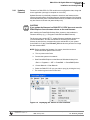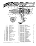
1
DNA-PPCx-1G PowerDNA Gigabit Ethernet I/O Cube User Manual March 2009 Edition PN Man-DNA-PPCx-1G-0309 Version 1.1 © Copyright 1998-2009 United Electronic Industries, Inc. All rights reserved. No part of this publication may be reproduced, stored in a retrieval system, or transmitted, in any form by any means, electronic, mechanical, by photocopying, recording, or otherwise without prior written permission. Information furnished in this manual is believed to be accurate and reliable. However, no responsibility is assumed for its use, or for any infringement of patents or other rights of third parties that may result from its use. All product names listed are trademarks or trade names of their respective companies. See the UEI website for complete terms and conditions of sale: http://www.ueidaq.com/company/terms.aspx Contacting United Electronic Industries Mailing Address: 27 Renmar Avenue Walpole, MA 02081 U.S.A. For a list of our distributors and partners in the US and around the world, please see http://www.ueidaq.com/ partners/ Support: Telephone:(508) 921-4600 Fax:(508) 668-2350 Also see the FAQs and online “Live Help” feature on our web site. Internet Support: Support:[email protected] Web-Site:www.ueidaq.com FTP Site:ftp://ftp.ueidaq.com Product Disclaimer: WARNING! DO NOT USE PRODUCTS SOLD BY UNITED ELECTRONIC INDUSTRIES, INC. AS CRITICAL COMPONENTS IN LIFE SUPPORT DEVICES OR SYSTEMS. Products sold by United Electronic Industries, Inc. are not authorized for use as critical components in life support devices or systems. A critical component is any component of a life support device or system whose failure to perform can be reasonably expected to cause the failure of the life support device or system, or to affect its safety or effectiveness. Any attempt to purchase any United Electronic Industries, Inc. product for that purpose is null and void and United Electronics Industries, Inc. accepts no liability whatsoever in contract, tort, or otherwise whether or not resulting from our or our employees' negligence or failure to detect an improper purchase. Table of Contents Chapter 1 The DNA-PPCx-1G Cube . . . . . . . . . . . . . . . . . . . . . . . . . . . . . . . . . . . . . . . . . . 1 1.1 Organization of Manual. . . . . . . . . . . . . . . . . . . . . . . . . . . . . . . . . . . . . . . . . . . . . . . . . 1 1.2 PowerDNA PPCx-1G System . . . . . . . . . . . . . . . . . . . . . . . . . . . . . . . . . . . . . . . . . . . . 3 1.3 Specifications . . . . . . . . . . . . . . . . . . . . . . . . . . . . . . . . . . . . . . . . . . . . . . . . . . . . . . . . 5 1.4 Key Features. . . . . . . . . . . . . . . . . . . . . . . . . . . . . . . . . . . . . . . . . . . . . . . . . . . . . . . . . 6 1.5 1.5.1 1.5.2 PowerDNA PPCx-1G Cube . . . . . . . . . . . . . . . . . . . . . . . . . . . . . . . . . . . . . . . . . . . . . 7 Cooling Air Flow . . . . . . . . . . . . . . . . . . . . . . . . . . . . . . . . . . . . . . . . . . . . . . . . 8 DNA Power, CPU, NIC, and I/O Layers . . . . . . . . . . . . . . . . . . . . . . . . . . . . . . 9 1.6 DNA-POWER-1GB Layer . . . . . . . . . . . . . . . . . . . . . . . . . . . . . . . . . . . . . . . . . . . . . . 11 1.7 DNA-PPCx-1G CPU Layer . . . . . . . . . . . . . . . . . . . . . . . . . . . . . . . . . . . . . . . . . . . . . 14 1.8 DNA-IO-Modules. . . . . . . . . . . . . . . . . . . . . . . . . . . . . . . . . . . . . . . . . . . . . . . . . . . . . 14 1.9 DC Power Thresholds. . . . . . . . . . . . . . . . . . . . . . . . . . . . . . . . . . . . . . . . . . . . . . . . . 14 Chapter 2 Installation and Configuration . . . . . . . . . . . . . . . . . . . . . . . . . . . . . . . . . . . . 15 2.1 2.1.1 2.1.2 Initial Installation Guide. . . . . . . . . . . . . . . . . . . . . . . . . . . . . . . . . . . . . . . . . . . . . . . . 15 Inspect Package . . . . . . . . . . . . . . . . . . . . . . . . . . . . . . . . . . . . . . . . . . . . . . 15 Install Software . . . . . . . . . . . . . . . . . . . . . . . . . . . . . . . . . . . . . . . . . . . . . . . 15 2.2 2.2.1 Initial Boot-up . . . . . . . . . . . . . . . . . . . . . . . . . . . . . . . . . . . . . . . . . . . . . . . . . . . . . . . 17 IP Addresses on the IOM . . . . . . . . . . . . . . . . . . . . . . . . . . . . . . . . . . . . . . . . 19 2.3 2.3.1 Improving Network Performance . . . . . . . . . . . . . . . . . . . . . . . . . . . . . . . . . . . . . . . . 20 Troubleshooting . . . . . . . . . . . . . . . . . . . . . . . . . . . . . . . . . . . . . . . . . . . . . . . 26 2.4 2.4.1 2.4.2 PowerDNA Explorer Quick-Start. . . . . . . . . . . . . . . . . . . . . . . . . . . . . . . . . . . . . . . . . 26 Updating Firmware. . . . . . . . . . . . . . . . . . . . . . . . . . . . . . . . . . . . . . . . . . . . . 29 Firmware Update Instructions . . . . . . . . . . . . . . . . . . . . . . . . . . . . . . . . . . . . 30 2.5 2.5.1 Mounting and Field Connections . . . . . . . . . . . . . . . . . . . . . . . . . . . . . . . . . . . . . . . . 32 Physical Dimensions . . . . . . . . . . . . . . . . . . . . . . . . . . . . . . . . . . . . . . . . . . . 32 2.6 Wiring . . . . . . . . . . . . . . . . . . . . . . . . . . . . . . . . . . . . . . . . . . . . . . . . . . . . . . . . . . . . . 33 2.7 Peripheral Termial Panel Wiring . . . . . . . . . . . . . . . . . . . . . . . . . . . . . . . . . . . . . . . . . 34 2.8 Repairing/ Upgrading Your DNA-PPCx-1G . . . . . . . . . . . . . . . . . . . . . . . . . . . . . . . . 34 2.9 Configuring a NIC Port for Diagnostic Mode. . . . . . . . . . . . . . . . . . . . . . . . . . . . . . . . 34 Chapter 3 PowerDNA Explorer . . . . . . . . . . . . . . . . . . . . . . . . . . . . . . . . . . . . . . . . . . . . . 42 3.1 The Main Window . . . . . . . . . . . . . . . . . . . . . . . . . . . . . . . . . . . . . . . . . . . . . . . . . . . 42 3.2 3.2.1 3.2.2 3.2.3 3.2.4 3.2.5 3.2.6 3.2.7 3.2.8 Menu Bar . . . . . . . . . . . . . . . . . . . . . . . . . . . . . . . . . . . . . . . . . . . . . . . . . . . . . . . . . File Menu . . . . . . . . . . . . . . . . . . . . . . . . . . . . . . . . . . . . . . . . . . . . . . . . . . . . Network Menu . . . . . . . . . . . . . . . . . . . . . . . . . . . . . . . . . . . . . . . . . . . . . . . . View Menu . . . . . . . . . . . . . . . . . . . . . . . . . . . . . . . . . . . . . . . . . . . . . . . . . . . Help Menu . . . . . . . . . . . . . . . . . . . . . . . . . . . . . . . . . . . . . . . . . . . . . . . . . . . Toolbar. . . . . . . . . . . . . . . . . . . . . . . . . . . . . . . . . . . . . . . . . . . . . . . . . . . . . . Device Tree . . . . . . . . . . . . . . . . . . . . . . . . . . . . . . . . . . . . . . . . . . . . . . . . . . Settings Panel . . . . . . . . . . . . . . . . . . . . . . . . . . . . . . . . . . . . . . . . . . . . . . . . Digital Input/Output Module Settings . . . . . . . . . . . . . . . . . . . . . . . . . . . . . . . 42 42 43 45 45 45 45 46 48 3.3 Analog Output Module Settings . . . . . . . . . . . . . . . . . . . . . . . . . . . . . . . . . . . . . . . . 53 3.4 Analog Input Module Settings . . . . . . . . . . . . . . . . . . . . . . . . . . . . . . . . . . . . . . . . . . 54 3.5 Counter/Timer Module Settings . . . . . . . . . . . . . . . . . . . . . . . . . . . . . . . . . . . . . . . . 55 Chapter 4 The DNA-PPCx-1G Core Module . . . . . . . . . . . . . . . . . . . . . . . . . . . . . . . . . . . 58 4.1 Device Architecture of the DNA-PPCx-1G Core Module . . . . . . . . . . . . . . . . . . . . . . 4.1.1 Primary Network Interface MII Port – NIC1 . . . . . . . . . . . . . . . . . . . . . . . . . . 4.1.2 Diagnostic Network Interface Port – NIC2 . . . . . . . . . . . . . . . . . . . . . . . . . . . 4.1.3 RS-232 Port . . . . . . . . . . . . . . . . . . . . . . . . . . . . . . . . . . . . . . . . . . . . . . . . . . 4.1.4 UBS 2.0 Dual Port (Controller and Slave) . . . . . . . . . . . . . . . . . . . . . . . . . . . 4.1.5 32MB Flash Memory . . . . . . . . . . . . . . . . . . . . . . . . . . . . . . . . . . . . . . . . . . . 4.1.6 128MB of SDRAM . . . . . . . . . . . . . . . . . . . . . . . . . . . . . . . . . . . . . . . . . . . . . 4.1.7 SYNC Port . . . . . . . . . . . . . . . . . . . . . . . . . . . . . . . . . . . . . . . . . . . . . . . . . . . 4.1.8 SD Card . . . . . . . . . . . . . . . . . . . . . . . . . . . . . . . . . . . . . . . . . . . . . . . . . . . . . 4.1.9 LEDs . . . . . . . . . . . . . . . . . . . . . . . . . . . . . . . . . . . . . . . . . . . . . . . . . . . . . . . 4.1.10 Watchdog Timer With Real-time Clock (Battery Backed) . . . . . . . . . . . . . . . 4.1.11 CPU/NIC Pinouts . . . . . . . . . . . . . . . . . . . . . . . . . . . . . . . . . . . . . . . . . . . . . . 59 60 60 60 60 60 60 60 60 60 60 61 Chapter 5 Programming Module-specific Functions . . . . . . . . . . . . . . . . . . . . . . . . . . . 62 5.1 Overview . . . . . . . . . . . . . . . . . . . . . . . . . . . . . . . . . . . . . . . . . . . . . . . . . . . . . . . . . . 62 5.2 Startup Sequence . . . . . . . . . . . . . . . . . . . . . . . . . . . . . . . . . . . . . . . . . . . . . . . . . . . 62 5.3 5.3.1 5.3.2 Setting Core Module Parameters . . . . . . . . . . . . . . . . . . . . . . . . . . . . . . . . . . . . . . . 63 Setting Parameters Via Serial Interface . . . . . . . . . . . . . . . . . . . . . . . . . . . . . 66 Clock and Watchdog Access . . . . . . . . . . . . . . . . . . . . . . . . . . . . . . . . . . . . . 68 5.4 5.4.1 5.4.2 5.4.3 5.4.4 Common Module (Layer) Interface . . . . . . . . . . . . . . . . . . . . . . . . . . . . . . . . . . . . . . Channel List . . . . . . . . . . . . . . . . . . . . . . . . . . . . . . . . . . . . . . . . . . . . . . . . . . Configuration Flags . . . . . . . . . . . . . . . . . . . . . . . . . . . . . . . . . . . . . . . . . . . . EEPROM User Area Access . . . . . . . . . . . . . . . . . . . . . . . . . . . . . . . . . . . . . PowerDNA Module Signaling. . . . . . . . . . . . . . . . . . . . . . . . . . . . . . . . . . . . . 69 69 71 72 74 Chapter 6 Host / IOM Communication . . . . . . . . . . . . . . . . . . . . . . . . . . . . . . . . . . . . . . . 77 6.1 6.1.1 Host / IOM Communication Modes . . . . . . . . . . . . . . . . . . . . . . . . . . . . . . . . . . . . . . . 77 Synchronous vs. Asynchronous. . . . . . . . . . . . . . . . . . . . . . . . . . . . . . . . . . . 77 6.2 6.2.1 6.2.2 Buffered I/O. . . . . . . . . . . . . . . . . . . . . . . . . . . . . . . . . . . . . . . . . . . . . . . . . . . . . . . . . 78 Advanced Circular Buffer (ACB) . . . . . . . . . . . . . . . . . . . . . . . . . . . . . . . . . . 79 Burst Mode. . . . . . . . . . . . . . . . . . . . . . . . . . . . . . . . . . . . . . . . . . . . . . . . . . . 81 6.3 6.3.1 6.3.2 6.3.3 6.3.4 6.3.5 Message Mode (Msg Protocol) . . . . . . . . . . . . . . . . . . . . . . . . . . . . . . . . . . . . . . . . . . IOM/Host Data Transfer. . . . . . . . . . . . . . . . . . . . . . . . . . . . . . . . . . . . . . . . . CAN-503 Data Transfer . . . . . . . . . . . . . . . . . . . . . . . . . . . . . . . . . . . . . . . . . PDNALib Structures. . . . . . . . . . . . . . . . . . . . . . . . . . . . . . . . . . . . . . . . . . . . Error Recovery. . . . . . . . . . . . . . . . . . . . . . . . . . . . . . . . . . . . . . . . . . . . . . . . Other Messaging Types. . . . . . . . . . . . . . . . . . . . . . . . . . . . . . . . . . . . . . . . . 6.4 6.4.1 6.4.2 Mapped I/O . . . . . . . . . . . . . . . . . . . . . . . . . . . . . . . . . . . . . . . . . . . . . . . . . . . . . . . . . 84 Fixed-Size Data Mapping (DMap) . . . . . . . . . . . . . . . . . . . . . . . . . . . . . . . . . 84 Variable-size Data Mapping (VMap) . . . . . . . . . . . . . . . . . . . . . . . . . . . . . . . 85 6.5 6.5.1 6.5.2 6.5.3 Choosing the Right Layers, Operating System, and Mode. . . . . . . . . . . . . . . . . . . . Attributes of Modes . . . . . . . . . . . . . . . . . . . . . . . . . . . . . . . . . . . . . . . . . . . . Application Requirements . . . . . . . . . . . . . . . . . . . . . . . . . . . . . . . . . . . . . . . Selecting the Right Mode for Your Application . . . . . . . . . . . . . . . . . . . . . . . 81 81 82 82 83 83 87 87 88 91 Chapter 7 DaqBIOS Protocol . . . . . . . . . . . . . . . . . . . . . . . . . . . . . . . . . . . . . . . . . . . . . . 93 7.1 DaqBIOS Packet Structure . . . . . . . . . . . . . . . . . . . . . . . . . . . . . . . . . . . . . . . . . . . . 93 7.2 DaqBIOS Protocol Versions . . . . . . . . . . . . . . . . . . . . . . . . . . . . . . . . . . . . . . . . . . . 95 7.3 7.3.1 7.3.2 Host and IOM Data Representa-tion. . . . . . . . . . . . . . . . . . . . . . . . . . . . . . . . . . . . . 95 Soft and Hard Real-time . . . . . . . . . . . . . . . . . . . . . . . . . . . . . . . . . . . . . . . . 95 DaqBIOS & Network Security . . . . . . . . . . . . . . . . . . . . . . . . . . . . . . . . . . . . 96 Chapter 8 DaqBIOS Engine . . . . . . . . . . . . . . . . . . . . . . . . . . . . . . . . . . . . . . . . . . . . . . . . 97 8.1 Basic Architecture . . . . . . . . . . . . . . . . . . . . . . . . . . . . . . . . . . . . . . . . . . . . . . . . . . . 97 8.2 Threads and Functions . . . . . . . . . . . . . . . . . . . . . . . . . . . . . . . . . . . . . . . . . . . . . . . 98 8.3 IOM Data Retrieval and Conversion . . . . . . . . . . . . . . . . . . . . . . . . . . . . . . . . . . . . 99 Chapter 9 Real-time Operation with an IOM . . . . . . . . . . . . . . . . . . . . . . . . . . . . . . . . . 100 9.1 Simple I/O . . . . . . . . . . . . . . . . . . . . . . . . . . . . . . . . . . . . . . . . . . . . . . . . . . . . . . . . 100 9.2 9.2.1 9.2.2 9.2.3 Real-time Data Mapping (RtDmap). . . . . . . . . . . . . . . . . . . . . . . . . . . . . . . . . . . . . Data Replication over the Network . . . . . . . . . . . . . . . . . . . . . . . . . . . . . . . RtDmap Functional Description . . . . . . . . . . . . . . . . . . . . . . . . . . . . . . . . . . RtDmap Typical Program Structure . . . . . . . . . . . . . . . . . . . . . . . . . . . . . . . 9.3 9.3.1 Real-time Variable-size Data Mapping (RtVmap) . . . . . . . . . . . . . . . . . . . . . . . . . . 104 RtVmap Typical Program Structure . . . . . . . . . . . . . . . . . . . . . . . . . . . . . . . 109 100 101 101 103 Appendix A Configuring Ethernet Cards. . . . . . . . . . . . . . . . . . . . . . . . . . . . . . . . . . . . . . 111 Appendix B Field Replacement of Fuses . . . . . . . . . . . . . . . . . . . . . . . . . . . . . . . . . . . . . 124 Index . . . . . . . . . . . . . . . . . . . . . . . . . . . . . . . . . . . . . . . . . . . . . . . . . . . . . . . . . . . . . . . . . 126 List of Figures Chapter 1 The DNA-PPCx-1G Cube . . . . . . . . . . . . . . . . . . . . . . . . . . . . . . . . . . . . . . . . . . 1 1-1 UEI Typical PowerDNA DNA-PPC8-1G System............................................................ 3 1-2 Technical Specifications ................................................................................................ 5 1-3 Product Features ........................................................................................................... 6 1-4 Typical DNA-PPCx-1G Cube with Stack Pulled Out...................................................... 7 1-5 DNA-IO-Filler Panel for unused slots............................................................................. 8 1-6 DNA-PPC5-1G Cube Air Flow ....................................................................................... 8 1-7 PowerDNA-PPCx-1G System Front Panel Arrangement .............................................. 9 1-8 DNA-PPCx-1G Front Panel LEDs................................................................................ 10 1-9 DNA-POWER-1GB DC Power and NIC Layer Front ................................................... 11 1-10 Functional Block Diagram of DNA-POWER-1GB Module ........................................... 12 1-11 Functional Block Diagram of DNA-PPCx-1G Core Module (2 Boards)........................ 13 Chapter 2 Installation and Configuration . . . . . . . . . . . . . . . . . . . . . . . . . . . . . . . . . . . . 15 2-1 Typical MTTTY Screen ................................................................................................ 18 2-2 Show System Configuration......................................................................................... 19 2-3 Single DNA-PPC-1G Cube Direct-Connected to Host without LAN Switch................. 21 2-4 Single Network for Operation/Diagnostics with 2 Cubes and LAN Switch................... 21 2-5 Separate Networks for Operation/Diagnostics with 2 Cubes and 2 LAN Switches...... 22 2-6 Typical Configuration for a Single DNA-PPC-1G with a LAN Switch........................... 25 2-7 Address Ranges to be Scanned .................................................................................. 27 2-8 Typical Screen for Analog Input Board ........................................................................ 28 2-9 Displaying the Version of Your Firmware..................................................................... 29 2-10 Update Firmware Menu Item ....................................................................................... 30 2-11 Password Dialog Box................................................................................................... 31 2-12 Firmware Update Progress Dialog Box........................................................................ 31 2-13 Physical Dimensions of DNA-PPCx-1G Cubes ........................................................... 32 2-14 System Configuration with LAN Switch........................................................................ 33 Chapter 3 PowerDNA Explorer . . . . . . . . . . . . . . . . . . . . . . . . . . . . . . . . . . . . . . . . . . . . . 42 3-1 PowerDNA Explorer Main Window .............................................................................. 42 3-2 Preferences.................................................................................................................. 42 3-3 Address Ranges Dialog Box ........................................................................................ 43 3-4 Edit Address Ranges Dialog Box................................................................................. 43 3-5 After a Network >>Scan Network................................................................................. 43 3-6 Password Dialog Box for “Store Config” and “Store All Configs” ................................. 44 3-7 Password Dialog Box for “Update Firmware. .”............................................................ 44 3-8 Example of a Wiring Diagram Display ......................................................................... 45 3-9 Example of the Device Tree......................................................................................... 46 3-10 Example of IOM Settings Panel for a DNA-PPCx-1G Cube ........................................ 46 3-11 Example of I/O Device Settings .................................................................................. 47 3-12 Screen from Network >> Read Input Data................................................................... 48 3-13 Example DIO-405 Inputs.............................................................................................. 49 3-14 Example DIO-405 Outputs........................................................................................... 50 3-15 Example of DIO-403 Inputs.......................................................................................... 51 3-16 Example of DIO-403 Outputs....................................................................................... 51 3-17 Example of DIO-403 Configuration .............................................................................. 52 3-18 Example DIO-403 In/Outputs....................................................................................... 52 3-19 Example AO-302 Module............................................................................................. 53 3-20 Example AI-201 Module............................................................................................... 54 3-21 Example CT-601 Module ............................................................................................. 55 3-22 Example Quadrature Controls ..................................................................................... 56 3-23 Example Bin Counter Controls..................................................................................... 56 3-24 3-25 3-26 Example Pulse Width Modulation (PWM) Controls...................................................... 56 Example Pulse Period Controls ................................................................................... 56 Example of Started Counter......................................................................................... 57 Chapter 4 The DNA-PPCx-1G Core Module . . . . . . . . . . . . . . . . . . . . . . . . . . . . . . . . . . . 58 4-1 PowerDNA Core Module – DNA-CPU/NIC-1G ............................................................ 58 4-2 FreeScale PowerPC CPU/NIC Controller Architecture................................................ 59 4-3 CPU / NIC Pinout Diagrams......................................................................................... 61 Chapter 5 Programming Module-specific Functions . . . . . . . . . . . . . . . . . . . . . . . . . . . 62 5-1 TCP/IP Properties ........................................................................................................ 68 5-2 Core Module Interconnection Diagram ........................................................................ 74 Chapter 6 Host / IOM Communication . . . . . . . . . . . . . . . . . . . . . . . . . . . . . . . . . . . . . . . 77 6-1 Communicating with an IOM........................................................................................ 77 6-2 Host / IOM Communication in ACB Mode (with DQE) ................................................. 79 6-3 Data Field of a RDFIFO Packet Containing Messages................................................ 82 6-4 Message Block for CAN messages in FIFO ................................................................ 82 6-5 Host / IOM COmmunication in DMap Mode................................................................. 84 6-6 Host / IOM Communication in VMap Mode (with DQE) ............................................... 85 Chapter 7 DaqBIOS Protocol . . . . . . . . . . . . . . . . . . . . . . . . . . . . . . . . . . . . . . . . . . . . . . 93 7-1 DaqBIOS Packet Over UDP Packet ............................................................................ 93 7-2 DaqBIOS Packet Over Raw Ethernet Packet .............................................................. 93 7-3 Host/IOM Packet Exchange in DaqBIOS Protocol....................................................... 95 Chapter 8 DaqBIOS Engine . . . . . . . . . . . . . . . . . . . . . . . . . . . . . . . . . . . . . . . . . . . . . . . . 97 8-1 User Application/DQE/IOM Interaction. ....................................................................... 97 Chapter 9 Real-time Operation with an IOM . . . . . . . . . . . . . . . . . . . . . . . . . . . . . . . . . 100 9-1 DMap Operation......................................................................................................... 100 Appendix A Configuring Ethernet Cards. . . . . . . . . . . . . . . . . . . . . . . . . . . . . . . . . . . . . . 111 Appendix B Field Replacement of Fuses . . . . . . . . . . . . . . . . . . . . . . . . . . . . . . . . . . . . . 124 B-1 Location of Fuse for PL-61x, PL-62x, and PL-63x Boards......................................... 124 B-2 Location of Fuses for DNR-POWER-1GB Board....................................................... 125 Index . . . . . . . . . . . . . . . . . . . . . . . . . . . . . . . . . . . . . . . . . . . . . . . . . . . . . . . . . . . . . . . . . 126 DNA-PPCx-1G Gigabit Ethernet Cube System Chapter 1 The DNA-PPCx-1G Cube Chapter 1 The DNA-PPCx-1G Cube This document describes the features, performance specifications, and operating functions of the PowerDNA Gigabit Ethernet Cube data acquisition system. The system is designed for use with an Ethernet Gigabit 1000 Base-T communication network. 1.1 Organization of Manual © Copyright 2009 United Electronic Industries, Inc. This DNA-PPCx-1G User Manual is organized as follows: • DNA-PPCx-1G Gigabit Ethernet Cube System This chapter provides an overview of a DNA-PPCx-1G system, component modules, features, accessories, and a list of all items you need for initial operation. • Installation and Configuration. This chapter summarizes the recommended procedures for installing, configuring, starting up, and troubleshooting a PPCx-1G system. • PowerDNA Explorer for the PPCx-1G This chapter provides a general description of the menus and screens of PowerDNA Explorer when used with a PPCx-1G system. • The DNA-PPCx-1G Core Module (CPU/NIC) This chapter describes the DNA-PPCx-1G CPU/NIC module, which contains a PowerPPC CPU and a GigE Network Interface Module. • Programming Board-specific Functions This chapter describes tools and facilities used for programming boardspecific functions. • HOST / IOM Communication This chapter describes the various operating modes that may be used in a PowerDNA PPCx-1G system for controlling communication between host and IOM. • DaqBIOS Protocol This chapter describes how the DaqBIOS protocol works. • DaqBIOS (DQE) Engine This chapter describes the operation and application of the DQE Engine. • Real-time Operation with an IOM This chapter discusses operation of the DNA-PPCx-1G system under control of a real-time operating system. • Appendix A – Configuring Additional Ethernet Cards This appendix describes procedures for installing and configuring additional Ethernet cards for us with various popular operating systems. • Appendix B – Field Replacement of Fuses • Index This is an alphabetical listing of topics covered in the manual, identified by page number. Tel: 508-921-4600 Date: March 2009 www.ueidaq.com Vers: 1.1 File: PPCx-1G_Chap1.fm 1 DNA-PPCx-1G Gigabit Ethernet Cube System Chapter 1 The DNA-PPCx-1G Cube Manual Conventions To help you get the most out of this manual and our products, please note that we use the following conventions: Tips are designed to highlight quick ways to get the job done, or reveal good ideas you might not discover on your own. NOTE: Notes alert you to important information. CAUTION! advises you of precautions to take to avoid injury, data loss, and damage to your boards or a system crash. Text formatted in bold typeface generally represents text you should enter verbatim. For instance, it can represent a command, as in the following example: “You can instruct users how to run setup using a command such as setup.exe.” Before plugging any I/O connector into the Cube or Board, be sure to remove power from all field wiring. Failure to do so may cause severe damage to the equipment. Usage of Terms In this document, the terms “module” and “layer” are used interchangeably. In PowerDNA Cubes, a “layer” refers to a data acquisition module (circuit board), which is typically assembled with other modules into a “multi-layer” stack for insertion into a PowerDNA Cube housing. © Copyright 2009 United Electronic Industries, Inc. Tel: 508-921-4600 Date: March 2009 www.ueidaq.com Vers: 1.1 File: PPCx-1G_Chap1.fm 2 DNA-PPCx-1G Gigabit Ethernet Cube System Chapter 1 The DNA-PPCx-1G Cube 1.2 PowerDNA PPCx-1G System The UEI PowerDNA DNA-PPCx-1G product is a GigE version of the popular PowerDNA Cube Ethernet-based Data Acquisition System. The DNA-PPC5-1G houses a PowerDNA Gigabit Ethernet data acquisition system in a 5-slot cube housing that can accept up to 3 I/O layers accessible from the front. Up to 4 cube systems may be mounted in a rack DNA-19RACKW accessory assembly. The DNA-PPC8-1G houses a PowerDNA Gigabit Ethernet data acquisition system in a 8-slot cube housing that can accept up to 6 I/O layers accessible from the front. Both 5- and 8-slot GigE Cubes are also available in fiber optic versions: (FPPC5-1G and FPPC8-1G). GigE Ports NIC1 NIC2 RS-232 Serial Port SD Card Slot USB A Port USB B Port Reset Button and Sync Connector Power In Connector LEDs I/O Layers (Up to 3 for PPC5-1G) (Up to 6 for PPC8-1G) Figure 1-1. UEI Typical PowerDNA DNA-PPC8-1G System As illustrated in Figure 1-4 and Figure 1-7, a standard PowerDNA PPCx-1G system consists of the following modules: • One 5-slot or 8-slot Cube Housing • One DNA-POWER-1GB DC Power Layer (topmost slot) • One DNA-PPC-1GB CPU layer (second slot) • Up to 3 (PPC5) or 6 (PPC8) DNA-IO-FILLER panels (one for each unused I/O slot) • DNR-PSU-24-100 100-Watt, 120/230 VAC to +24VDC External Power Supply with cable and Molex connector for plug-in to the Molex Power In connector on the front panel. To configure a complete data acquisition system, insert up to 3 (or 6) DNA I/O layers into the Cube housing, which may be specified in any combination of the following types: • © Copyright 2009 United Electronic Industries, Inc. DNA-AI-201, -202, 205, 207, -208, -211, -224, -225 Tel: 508-921-4600 Date: March 2009 www.ueidaq.com Vers: 1.1 File: PPCx-1G_Chap1.fm 3 DNA-PPCx-1G Gigabit Ethernet Cube System Chapter 1 The DNA-PPCx-1G Cube • DNA-AO-308, -308-350, -308-353, -308-420, -332, -333 • DNA-DIO-401, -402, -403, 404, -405, 406, -416, -432, -433, -448 • DNA-CT-601, DNA-QUAD-604 • DNA-SL-501, DNA-CAN-503 • DNA-429-566, DNA-429-512 • DNA-GPS • Any future additions to the PowerDNA I/O module product line Note: Refer to www.ueidaq.com for a description of each I/O module. © Copyright 2009 United Electronic Industries, Inc. Tel: 508-921-4600 Date: March 2009 www.ueidaq.com Vers: 1.1 File: PPCx-1G_Chap1.fm 4 DNA-PPCx-1G Gigabit Ethernet Cube System Chapter 1 The DNA-PPCx-1G Cube 1.3 Specifications Figure 1-2 lists the technical specifications of a PowerDNA DNA-PPCx-1G Cube. Technical Specifications: Standard Interfaces Gigabit Ethernet Two independent 1000/100/10Base-T interfaces, each with a unique IP address (connected via standard RJ-45 connectors) USB 2.0 Two ports, one controller, one slave Config/General RS-232, 9-pin “D” Sync Custom cable to sync multiple cubes I/O Slots Available DNA-PPC8g 6 slots DNA-PPC5g 3 slots Host Communications 100 meters max, CAT5+ cable Distance from host Ethernet data 20 megabyte per second transfer rate >6 megasample per second. Capable of susAnalog data tained transfer of any cube configuration transfer rate DMAP I/O mode update 1000 I/O channels (analog and/or digital) in less than 1 millisecond, guaranteed Processor CPU Freescale 8347 series, 400 MHz, 32-bit Memory 128 MB (not including on-board Flash) Status LEDs Attention, Read/Write, Power, Communications Active Environmental Temp (operating) Tested to -40 °C to 85 °C Temp (storage) -40 °C to 100 °C Humidity 0 to 95%, non-condensing Vibration (IEC 60068-2-64) 10–500 Hz, 5 g (rms), Broad-band random (IEC 60068-2-6) 10–500 Hz, 5 g, Sinusoidal Shock (IEC 60068-2-27) 50 g, 3 ms half sine, 18 shocks at 6 orientations; 30 g, 11 ms half sine, 18 shocks at 6 orientations Altitude 70,000 feet, maximum MTBF 300,000 hours Physical Dimensions DNA-PPC5g 4.1” x 4.0” x 4.0” DNA-PPC8g 4.1” x 4.0” x 5.8” Power Requirements Voltage 9 - 36 VDC (AC adaptor included) Power Dissipation 13 W at 24 VDC (not including I/O boards) Figure 1-2. Technical Specifications © Copyright 2009 United Electronic Industries, Inc. Tel: 508-921-4600 Date: March 2009 www.ueidaq.com Vers: 1.1 File: PPCx-1G_Chap1.fm 5 DNA-PPCx-1G Gigabit Ethernet Cube System Chapter 1 The DNA-PPCx-1G Cube 1.4 Key Features The following table is a list of key features of a DNA-PPCx-1G PowerDNA Cube. Easy to configure and deploy Over 30 different I/O boards available Built-in signal conditioning Gigabit Ethernet based (100/10Base-T compatible) Flange kit for mounting to wall/flat surface DIN rail and Rack Mount kits Attach style carrying case available for portable deployments Standard “Off-the-shelf” products and delivery True Real-time Performance 1 msec updates guaranteed with 1000 I/O Up to 6 million samples per second Use QNX, RTX, RT Linux, RTAI Linux, LabVIEW RT Flexible Connectivity Dual 1000Base-T Gigabit Ethernet ports with independent IPs Dual USB 2.0 controller ports 10/100Base-FX Fiber interface available (see DNA-FPPC family) Supports WIFI / GSM / Cell networks Compact Size: 4.1” x 4” x 5.8 Cube holds 6 I/O boards 4.1” x 4” x 4” Cube holds 3 I/O boards 150 analog inputs per cube, 192 analog outputs per cube 288 digital I/O bits per cube. 48 counter/quadrature channels per cube 72 ARINC 429 ports per cube 24 Serial or CAN ports per cube Low Power: Less than 13 watts per cube (not including I/O boards0 AC, 9-36 VDC or battery powered. Stand alone and Data Logger Modes DNA-PPC-G series Cubes can be upgraded with UEI-LOGGER series capabilities DNA-PPC-G series Cubes can be upgraded to the Linux based UEIPAC Programmable Automation Controller Rugged and Industrial: All Aluminum construction Operation tested from -40°C to 85°C Vibration tested to 5 g, (operating) Shock tested to 50 g (operating) All I/O isolated from Cube and host PC. Operation to 70,000 feet Outstanding Software support Windows, Linux, RT Linux, Windows RT, RTX, VXworks and QNX operating systems VB, VB .NET, C, C#, C++, J# MATLAB, LabVIEW, DASYLab, OPC, ActiveX support Figure 1-3. Product Features © Copyright 2009 United Electronic Industries, Inc. Tel: 508-921-4600 Date: March 2009 www.ueidaq.com Vers: 1.1 File: PPCx-1G_Chap1.fm 6 DNA-PPCx-1G Gigabit Ethernet Cube System Chapter 1 The DNA-PPCx-1G Cube 1.5 PowerDNA PPCx-1G Cube Each DNA-PPCx-1G cube contains a two-layer Core Module with status indicating LEDs, serial port, A and B USB ports, two GigE network interface ports, an SD card reader, power circuits, reset button/sync interface. The Core Module contains a GigE CPU and two Network Interface Control (NIC) ports, one for controlling up to 6 I/O layers mounted in the cube, and another for diagnostic functions. The device-specific I/O boards are functionally identical to the corresponding modules for the PowerDNR RACKtangle.The only differences between the two types relate to the mounting arrangements. Figure 1-4. Typical DNA-PPCx-1G Cube with Stack Pulled Out As shown in Figure 1-4 and Figure 1-7, the PowerDNA PPCx-1G enclosure is designed to house the following items: • One isolated DNA-POWER-1GB DC/DC Power Module/Power Monitor with RJ-45 connectors for NIC2 and NIC2, DB-9 connector for a serial port, and A and B USB controller/slave ports (future use). • One DNA-PPC-1GB CPU module with 8 indicating LEDs, sync connector, reset pushbutton, SD card slot, and a 4-pin Molex Power In connector. • Up to 3 (PPC5) or 6 (PPC8) PowerDNA I/O layers (boards) functionally identical to PowerDNR I/O boards but designed for mounting in a DNA cube housing • Blank filler panels for all unused slots • One (for PPC5) or two (for PPC8) 8-volt cooling fans mounted on the rear cover of the Cube The cube itself is a rigid, extruded aluminum, mechanical structure with complete EMI shielding. Unused slots are filled with blank filler panels. The DC power module provides output voltages of 24, 3.3, 2.5, 1.5, and 1.2 VDC for the logic/CPU and 8 VDC to power the cooling fans. © Copyright 2009 United Electronic Industries, Inc. Tel: 508-921-4600 Date: March 2009 www.ueidaq.com Vers: 1.1 File: PPCx-1G_Chap1.fm 7 DNA-PPCx-1G Gigabit Ethernet Cube System Chapter 1 The DNA-PPCx-1G Cube Faceplate Blank Filler Plate(s) for unused opening(s) in faceplate Figure 1-5. DNA-IO-Filler Panel for unused slots 1.5.1 Cooling Air Flow As shown in Figure 1-6, cooling is drawn into the rear of the enclosure, routed forward over the electronic circuit boards, up to the top of the enclosure, and then out the top rear of the enclosure. The system is designed to maintain positive pressure cooling within the enclosure at all times. Backplate POWER layer Connector for fan power (on NIC layer) Exhaust CPU/NIC layer Snap-0n Cover and Air Filter Air Flow I/O 1 layer I/O 2 layer I/O 3 layer Fan(s) (See Figure 1-8) Faceplate Exhaust through slotted vents Extruded Aluminum Housing Figure 1-6. DNA-PPC5-1G Cube Air Flow © Copyright 2009 United Electronic Industries, Inc. Tel: 508-921-4600 Date: March 2009 www.ueidaq.com Vers: 1.1 File: PPCx-1G_Chap1.fm 8 DNA-PPCx-1G Gigabit Ethernet Cube System Chapter 1 The DNA-PPCx-1G Cube 1.5.2 DNA Power, This section describes the basic modules included in every DNA-PPCx-1G system – the CPU/NIC layer, the DC power layer, and I/O layers. CPU, NIC, and I/O Layers Serial Port NIC 1 Port NIC 2 Port with 2 LEDs with 2 LEDs Sync Reset Connector Button USB B port USB A port (controller) (slave) (future use) (future use) Power In User Needs Controlled Attention or OFF 3.3V 24V ! USR 3.3 24 R/W COM PG Hi Read/ Comm. Pwr Temp Write Active Good Active I/O Layer(s): Ready LED Status (Active) LED I/O Cable Connector Figure 1-7. PowerDNA-PPCx-1G System Front Panel Arrangement © Copyright 2009 United Electronic Industries, Inc. Tel: 508-921-4600 Date: March 2009 www.ueidaq.com Vers: 1.1 File: PPCx-1G_Chap1.fm 9 DNA-PPCx-1G Gigabit Ethernet Cube System Chapter 1 The DNA-PPCx-1G Cube Figure 1-8 describes the conditions indicated by the LEDs on the front of each module in the rack. An LED ON means: -Needs Attention (Red) Hi Temp User Controlled or OFF (default) 3.3V OK/Error SD Card Reader 24V OK/Error Reset Button SD Card Read/Write Active I/O Comm. Active (flashes once/second) Power Good Sync Connector 4-pin Molex Power In connector Figure 1-8. DNA-PPCx-1G Front Panel LEDs Figure 1-8 describes the meanings of various states of the indicating LEDs mounted on the front panel of the PPCx-1G Cube. The LEDs are physically mounted on the CPU Layer, which in located in the second topmost layer position form the top of the Cube. A temperature sensor mounted on the DNA-Power-DC Layer monitors internal temperature continuously, turning fan(s) on if the internal temperature exceeds 45°C, off if it falls below 45°C, and shutting down power if a high limit is exceeded. © Copyright 2009 United Electronic Industries, Inc. Tel: 508-921-4600 Date: March 2009 www.ueidaq.com Vers: 1.1 File: PPCx-1G_Chap1.fm 10 DNA-PPCx-1G Gigabit Ethernet Cube System Chapter 1 The DNA-PPCx-1G Cube 1.6 DNA-POWER- The DNA-POWER-1GB Layer has a dedicated DC/DC source available for use with the PowerDNA PPCx-1G Cube. It is always mounted in the topmost slot of 1GB Layer the cube and is recognized on the PowerDNA bus with an ID of 0x020 at address 0xA00C0000. The non-isolated side (NIS) logic complies with full common logic interface (CLI) implementation. The key features of the unit are: • Input power — 9-36 VDC 80W maximum, protected by resettable fuses and EMI chokes • Output power sources (all with greater than 90% efficiency) 24V, 1A (24W) 3.3V, 5A (16.5W, including the 2.5V derived voltage) 2.5V, 3A (derived from 3.3V source) 1.5V, 5A, (7.5W, including the 1.2V derived voltage) 8V, 0.5A (4W for fans) • DC/DC for 24V, 3.3V, and 1.5V are synchronized from the single spreadspectrum clock source in the CPU/NIC Core Module for low EMI noise level • Output Power provided for Fan control (Forced ON) and status ON/OFF • Monitoring and LED indicators (1% accuracy, 0.25Hz update rate, mounted on CPU Layer) for: – All output voltages – Input current for the 9-36VDC for the DNA Cube Housing – All voltages from the NIC/Power Module (24V, 3.3V, 2.5V) – Temperature of the DNA-PPCx Cube Housing and layers • Onboard FPGA logic chip is CYCLONE EP1C3/C6T144 • TI MSP4300 microcontroller used for logic reprogramming • Provides 9-36VDC for all modules from an external power source USB slave port (not used) DB-9 Connector for Serial Port NIC1 RJ45 Connector NIC2 RJ45 Connector USB controller port (not used) Figure 1-9. DNA-POWER-1GB DC Power and NIC Layer Front © Copyright 2009 United Electronic Industries, Inc. Tel: 508-921-4600 Date: March 2009 www.ueidaq.com Vers: 1.1 File: PPCx-1G_Chap1.fm 11 DNA-PPCx-1G Gigabit Ethernet Cube System Chapter 1 The DNA-PPCx-1G Cube A functional block diagram of the DNA-POWER-1GB Module is shown in Figure 1-10 below. Input Voltage Source 9-36 VDC @ 80 W max. 3.3V DC/DC Input Current Monitor 2.5V LDO 1.5V DC/DC 24V DC/DC 8V FAN DC/DC FAN1-2 CONTROL 3.3V DC/DC Vin 24V 8V 1.2V 1.5V 24V 2.5V 3.3V FAN3-4 CONTROL 3.3V DC/DC 24-bit ADC (LTC2498) 13 sources: +2.5V, +2.5VNIC, 3.3V, +3.3VNIC, +24Vm +24VNIC, +VIN, +1.5V, +1.2V, +8V FAN, Iin, TEMP1 (TCPOS), TEMP2 (TCNEG). Voltage sources use 1:23.1 dividers on the front end, except for the Vin, which uses a 1:45.3 divider. +2.5V NIC +3.3V NIC +24V NIC TEMP1 TEMP2 DNR Bus Connector 1.2V LDO Standard NIC-logic plus: Access to ADC data readings Fan 1-2 and 3-4 ON/OFF control Fan ON/OFF status 12 LEDs ON/OFF control LED block – 12 status LEDs Figure 1-10. Functional Block Diagram of DNA-POWER-1GB Module As shown in Figure 1-10, the DNA-POWER-1GB Module operates as follows: A 9-36VDC voltage input (Vin) from an external source is connected to the board through a resettable fuse. The board monitors the input current and passes Vin to the DNA bus as Vout. Vout also is connected to DC/DC converters that produce 24 VDC, 3.3VDC and 1.5VDC output voltages, which are also placed on the DNA bus. Both 3.3 and 1.5VDC voltages are connected to low dropout regulators that, in turn, generate the 2.5VDC and 1.2VDC output voltages on the bus. The 24VDC source is fed to a low dropout regulator that produces 8VDC to drive the cooling fans (through fan controller chips). © Copyright 2009 United Electronic Industries, Inc. Tel: 508-921-4600 Date: March 2009 www.ueidaq.com Vers: 1.1 File: PPCx-1G_Chap1.fm 12 DNA-PPCx-1G Gigabit Ethernet Cube System Chapter 1 The DNA-PPCx-1G Cube The input current and all output voltages, including the +2.5, +3.3, and +24VDC from the NIC module, plus signals from the temperature sensor mounted within the enclosure, are input to a 24-bit delta-sigma A/D converter. Except for Vin, the voltage sources use 1:23.1 dividers on the front end. Vin uses a 1:45.3 divider. Figure 1-11 shows a functional block diagram of a DNA-PPCx-1G Core Module, which consists of a CPU/NIC Layer and a DNA-POWER-1G DC layer, assembled in a PPCx-1G Cube.. . 32-bit 66-MHz bus RTC FLASH 1000-BASE-T RJ-45 PHY MII MAC DDR2 FPGA RJ-45 PHY MII MAC PPC 8347 Power In 9-36V DC Input DC/DC SD Card RS-232 USB 2.0 USB 2.0 Power Out Figure 1-11. Functional Block Diagram of DNA-PPCx-1G Core Module (2 Boards) As shown in Figure 1-11, the Core Module uses a Freescale (formerly Motorola) PowerPC 8347 400 MHz, 32-bit processor, with ___ Flash Memory and 128MB DDR2 Memory. Two independent gigabit Ethernet Network Interface Controllers (NICs) are provided, each with its own IP address. One, usually NIC1, is configured as a main control port and the other, NIC2, as a diagnostic port. Either port may be asssigned either function.An FPGA provides the logic for controlling all system operation and offers a convenient mechanism for modifying and extending system functions. The CPU Layer (second topmost layer position) also provides 8 indicating LEDs, a recessed manual reset button, sync bus connector for connection to other Cubes and systems, SD Card Read/Write unit, and 4-pin Molex connector for 9-36 VDC incoming power. The associated DNA-POWER-1G module (topmost layer position) has an RS232 serial port with DB-9 front panel connector, two RJ-45 connectors (each with two green LEDs) for the NIC1 and NIC2 Ethernet ports, two USB 2.0 ports (A and B connectors) for USB host and slave connections (for future use – not currently active), plus a board-mounted connector at the rear of the board for supplying power to cooling fans on the rear cover of the Cube. © Copyright 2009 United Electronic Industries, Inc. Tel: 508-921-4600 Date: March 2009 www.ueidaq.com Vers: 1.1 File: PPCx-1G_Chap1.fm 13 DNA-PPCx-1G Gigabit Ethernet Cube System Chapter 1 The DNA-PPCx-1G Cube A temperature sensor mounted on the POWER layer monitors temperature within the Cube above the CPU. The system turns on the fan(s) if temperature exceeds 45° C and shuts down power to the Cube if a high limit is exceeded. 1.7 DNA-PPCxThe DNA-PPCx-1G CPU/NIC Layer contains a PowerPC 8347 CPU and 1G CPU Layer associated Network Interface Control (NIC) logic that controls all Ethernet communication functions. The unit has a dual 1GB Ethernet module. 1.8 DNA-IOModules UEI I/O modules are available either as PowerDNA versions for use with PPCx Cubes or as PowerDNR versions for installation in a DNR rack enclosure. Both versions are functionally identical. The only difference between them is the physical mounting arrangement. For detailed electrical specifications and user instructions for a specific DNA I/O board, refer to the datasheets and User Manuals for that specific layer. These documents are available for examination and download from the UEI website at www.ueidaq.com. 1.9 DC Power Thresholds Table 5-1 lists the DC power threshold specifications for PPCx-1G Cubes. Table 5-1 DC Power Thresholds for DNA-PPCx-1G Cubes Backplane Power Rail Voltages Logic power supply Turn-on Voltage, V1 Turn-off Reset Voltage, V Voltage, V2 Notes 7.2 7.0 Supplies power to all CPUs and FPGAs. Cube can communicate with Ethernet when CPU is functional Analog power supply is used as a regulated source for on-layer DC/DCs on most layers +3.3V, +2.5V, +1.5V, +1.2V 7.5 Analog power supply +24V 8.5 - 7.8 Fan power supply +12V 8.5 - 8.4 On-layer DC/ DCs that use input power +VIn 7.8-8.8 - 7.5-8.5 (When Vin is below 7.2V, a voltage reset puts all layers into reset mode.) Varies with layer type. 1. Turn-on, V: The value of Vin at which the corresponding DC/DCs are turned on. 2. Turn-off, V: The value of Vin at which the corresponding DC/DCs are turned off. NOTE: A DNA-PPC-1GB core module consumes only 70mW when Vin is below 7V. © Copyright 2009 United Electronic Industries, Inc. Tel: 508-921-4600 Date: March 2009 www.ueidaq.com Vers: 1.1 File: PPCx-1G_Chap1.fm 14 DNA-PPCx-1G Gigabit Ethernet Cube System Chapter 2 Installation and Configuration Chapter 2 Installation and Configuration Installation consists of: 2.1 2.1.1 Initial Installation Guide Inspect Package • DNA-PPCx-1G hardware setup • PowerDNA software package installation • Configuration This section describes the procedure recommended for performing an initial hardware and software setup when you first receive a DNA-PPCx-1G system. Inspect the contents of the shipping package. With a standard DNA-PPCx-1G system, you should find: • A PPC5 or PPC8 5- or 8-slot enclosure, preinstalled with a DNA-PPCx1G CPU Layer, a DNA-POWER-DC power and NIC Layer, blank filler panels, plus your selection of I/O Boards. • A DNA-PSU-24-100 100-watt1 universal powerline brick that plugs into an AC outlet and provides 24V dc output. The supply comes with a power cord for the mains and an adapter cable ending in a Molex connector for plugging into the DNA-POWER-DC layer. • DB-9 serial cable for initial hardware configuration and firmware downloading. • CD-ROM with support software NOTE: Depending on your application, you may also need to provide the following items not normally included with your order (see Figures 2-3 to 2-6 on pages 21 to 25): 2.1.2 Install Software • CAT5e cables between host and DNA system NIC1 primary port, and/or between host and an Ethernet switch, and/or between switch and DNA primary port • CAT5e cables between host and DNA system secondary (diagnostic) NIC2 port, between host and an Ethernet switch, and/or between switch and DNA secondary (diagnostic) port This section describes how to load the PowerDNA software suite onto a Windows- or Linux-based computer and run some initial tests. The latest PowerDNA support software is online at www.ueidaq.com/download; a known working copy is also on the PowerDNA Software Suite CD. A. Software Install: Windows 9x/2000/XP The PowerDNA CD provides one installer that combines the UEI low-level driver and UEIDAQ Framework. 1. A larger power supply may be required for some configurations. Refer to UEI. © Copyright 2009 United Electronic Industries, Inc. Tel: 508-921-4600 Date: January 2009 www.ueidaq.com Vers: 1.0 File: PPCx-1G_Chap2.fm 15 DNA-PPCx-1G Gigabit Ethernet Cube System Chapter 2 Installation and Configuration The installer automatically searches for third-party IDE and testing suites, and adds them as tools to the suites found. Be sure to install third-party applications (such as LabVIEW, MATLAB, or MsVS2003) before installing the PowerDNA Software Suite. To install the PowerDNA Software Suite, do the following: STEP 1: Log in as Administrator. STEP 2: Run Setup a. Insert the PowerDNA Software Suite CD into your CD-ROM drive. Windows should automatically start the PowerDNA Setup program. An installer with the UEI logo and then PowerDNA Welcome screen should appear. If none appears, run setup.exe from the CD drive: Start >> Run >> d:\setup.exe >> OK. If you downloaded the most recent executable from www.ueidaq.com, double-click on the filename to run the executable. b. Choose the PowerDNA Software Suite option. c. Unless you are an expert user and have specific requirements, select Typical Installation and accept the default configuration. The Software Suite installer requires and automatically installs Sun’s Java VM (JRE) for you, in addition to the full complement of tools. As an alternative, use the Custom option to display and ensure that all of the necessary packages are installed. -- Companion Documentation: Quick Start Guide, Configuration and Core Module, I/O Board Manuals, Low-Level Programming Guide – SDK: includes/lib for C/Java, examples, and Sun’s JRE; (The SDK is not the UeiDaq Framework). – PowerDNA Apps: PowerDNA Explorer, MTTTY – PowerDNA Components (including DLL files) – PowerDNA Firmware d. Click Next to continue through the dialogs. e. Click Finish to complete the installation; restart the computer. This Software Suite installed the bare-minimum tools needed in later steps: MTTTY, PowerDNA Explorer, and the low-level driver. UEIDAQ Framework provides the structure for developing applications under C/C++, C#, VB.NET, ActiveX (VB6, Delphi), MATLAB, LabVIEW, DASYLab, LabWindows/CVI, OPC, and other programming languages. NOTE: Because the installation process modifies your Windows registry, you should always install or uninstall the software using the appropriate utilities. Never remove PowerDNA software from your PC directly by deleting individual files; always use the Windows Control Panel Add/Remove Programs utility. © Copyright 2009 United Electronic Industries, Inc. Tel: 508-921-4600 Date: January 2009 www.ueidaq.com Vers: 1.0 File: PPCx-1G_Chap2.fm 16 DNA-PPCx-1G Gigabit Ethernet Cube System Chapter 2 Installation and Configuration B. Software Install: Linux Linux: The PowerDNA_*.tgz file in the CD\Linux folder contains the software package for Linux. To extract the file to a local directory: tar -xjvf /path/to/powerdna*.tgz Follow the instructions in the readme.txt file contained therein. 2.2 Initial Boot-up Perform an initial boot in preparation for configuring the network, using the following procedure: STEP 1: Familiarize yourself with the Cube system front-panel layout. Note that all external connections are made on the front of the unit. STEP 2: Attach the serial cable to the host PC and to the RS-232 port on the front panel of the Cube. a. Run a terminal-emulation program (MTTTY) on the PC. Any terminalemulation program, except HyperTerminal, may be used (MTTTY, Minicom, TeraTerm, etc.). b. Verify that COM parameters are set at: 57600 baud, 8 bits, no parity, 1 stop bit. c. Click Connect in MTTTY, or use the commands on one of the other terminal-emulation programs to establish communication with the Cube. STEP 3: Connect power to the system (9-36V DC) by plugging the Molex-type power connector from the power supply into the mating connector on the front panel of the unit. The power source may be the bundled DNA-PSU-24-100 100 watt powerbrick or a user-supplied source. Note that the DNA-PSU-24-100 plugs into a 100 - 240V, 47- 63 Hz outlet and outputs up to 4.17A at 24 VDC. STEP 4: Turn on power to the Cube. © Copyright 2009 United Electronic Industries, Inc. Tel: 508-921-4600 Date: January 2009 www.ueidaq.com Vers: 1.0 File: PPCx-1G_Chap2.fm 17 DNA-PPCx-1G Gigabit Ethernet Cube System Chapter 2 Installation and Configuration STEP 5: As soon as the system powers up, it runs through self-diagnostic mode and generates output on the terminal program. A typical readout might be as shown in Figure 2-1: Figure 2-1. Typical MTTTY Screen The boot process displays the model, serial number, and slot positions of boards in the cube. Type show <CR> to display information on system configuration, as illustrated in Figure 2-2. © Copyright 2009 United Electronic Industries, Inc. Tel: 508-921-4600 Date: January 2009 www.ueidaq.com Vers: 1.0 File: PPCx-1G_Chap2.fm 18 DNA-PPCx-1G Gigabit Ethernet Cube System Chapter 2 Installation and Configuration Figure 2-2. Show System Configuration All parameters can be changed; most notably, the IP address, gateway, and subnet mask (netmask) configured for this system. 2.2.1 IP Addresses on the IOM The DNA-PPCx-1G ships with preconfigured factory default IP addresses for NIC1 and NIC2 in nonvolatile memory (usually 192.168.100.2 for NIC1 and 192.168.100.102 for NIC2). These are static IP addresses; the system never retrieves its IP address from a DHCP server. This section describes why and how to change the default IP addresses. Should you change the IP Address? Yes, if you plan to use the DNA-PPCx-1G on a LAN in which. • High sampling rate is not necessary. • Some samples can be dropped due to network congestion and collisions. • The system should be accessible by multiple parties on the LAN. • Multiple Cubes/systems operate (and interact) on the same network. Alternatively, if you plan to use the system for high-speed measurements where high reliability is necessary – a direct connection between the host PC and a NIC1 is recommended. For a direct connection, refer to “Improving Network Performance” on page 20. How to change the IP address of the primary Ethernet port. Both PowerDNA Explorer and a terminal-emulation program can be used to change IP addresses. Consult your system or network administrator to obtain unused IP addresses. Let’s say, for example, that your system administrator assigns you the IP 192.168.0.65 for the primary port of your IOM. 1.NIC - Network Interface Controller; a commercially available Ethernet (i.e. IEEE 802.3-2005) adapter. © Copyright 2009 United Electronic Industries, Inc. Tel: 508-921-4600 Date: January 2009 www.ueidaq.com Vers: 1.0 File: PPCx-1G_Chap2.fm 19 DNA-PPCx-1G Gigabit Ethernet Cube System Chapter 2 Installation and Configuration To change the IP, using the terminal program, enter the following commands: DQ> set ip 192.168.0.65 Enter user password > powerdna // Sets this system IP to 192.168.0.65 // The default password is “powerdna” // Saves the newly changed configuration // Reboots the system for the new IP to //take effect DQ> store DQ> reset In this manner, you can set any parameters listed with the “show” command. Connect the DNA-PPCx-1G system to your switch with a CAT5e cable. If you can establish communication with a DNA-PPC-1G CPU, but later want to modify the IP address, you can also do so from within PowerDNA Explorer. After the exploratory process, go to the field where the application displays the IP address. You then enter the new IP address and hit <Return>. This action downloads the new IP address into the system’s non-volatile memory. You might also need to change the gateway and network mask to match settings on your LAN. How to change the IP address of the secondary (diagnostic) Ethernet port. To change the IP address of the secondary port (NIC2), use the terminal program as with the primary port, but instead use the command: set ip2 aaa.bbb.ccc.ddd where aaa.bbb.ccc.ddd is the new IP address for the secondary port. Then proceed the same as with the primary port. 2.3 Improving Network Performance © Copyright 2009 United Electronic Industries, Inc. To improve DNA-PPCx-1G network performance, we recommend that instead of connecting to a company-wide network, you use separate commercially available network interface controller (NIC) cards and, where possible, set up a single dedicated mini-network for DNA-PPC-1G Cubes for both operation and diagnostics, as shown in Figure 2-4. As an alternative, you can configure two separate networks, one for operation and one for diagnostic purposes, as shown in Figure 2-5. If you do not need to connect to a company LAN and have only a single DNA-PPC-1G Cube in your system, you can connect it directly to your host as shown in Figure 2-3. Tel: 508-921-4600 Date: January 2009 www.ueidaq.com Vers: 1.0 File: PPCx-1G_Chap2.fm 20 DNA-PPCx-1G Gigabit Ethernet Cube System Chapter 2 Installation and Configuration NIC1 - 192.168.1.10 (Primary Port) NIC2 - 192.168.100.3 (Diagnostic Port) Figure 2-3. Single DNA-PPC-1G Cube Direct-Connected to Host without LAN Switch Figure 2-4 shows a two-cube single network system with a LAN switch that performs both data acquisition and diagnostic functions. NIC1 – 192.168.1.10 NIC2 - 192.168.100.3 Diagnostics Figure 2-4. Single Network for Both Operation and Diagnostics Using Two DNA-PPC-1G Cubes and LAN Switch © Copyright 2009 United Electronic Industries, Inc. Tel: 508-921-4600 Date: January 2009 www.ueidaq.com Vers: 1.0 File: PPCx-1G_Chap2.fm 21 DNA-PPCx-1G Gigabit Ethernet Cube System Chapter 2 Installation and Configuration Figure 2-5 shows a two-cube dual network system with two LAN switches that performs both data acquisition and diagnostic functions. NIC1 - to Intranet NIC2 Diagnostic Ports Figure 2-5. Separate Networks for Operation and Diagnostics Using Two DNA-PPC-1G Cubes and Two LAN Switches For example, assume that your office uses a Class C network (the class intended for small networks with fewer than 256 devices) and your host is configured with a static IP or via DHCP — Dynamic Host Configuration Protocol — a protocol for assigning dynamic IP addresses to devices on a network. STEP 1: Obtain your networking configuration by using the Command Prompt: Start >> Programs >> (Accessories>>) Command Prompt C:\> ipconfig Ethernet adapter NIC1 - Local Connection-specific DNS IP Address. . . . . . . 192.168.1.10 Subnet Mask . . . . . . 255.255.255.0 Area Connection: Suffix . : . . . . . : . . . . . : Default Gateway . . . . .. . . .: 192.168.1.1 Linux users can use the more verbose “ifconfig” command instead. In the following example, the subnet range 192.168.1.0 — 192.168.1.255 is used by NIC1. © Copyright 2009 United Electronic Industries, Inc. Tel: 508-921-4600 Date: January 2009 www.ueidaq.com Vers: 1.0 File: PPCx-1G_Chap2.fm 22 DNA-PPCx-1G Gigabit Ethernet Cube System Chapter 2 Installation and Configuration IP Addressing: The range of usable addresses is defined by the IP address and subnet maskAn IP address is a number that lies within the range of 0.0.0.0 and 255.255.255.255. Here, the IP address is 192.168.1.10. The subnet mask indicates where an address stops. For example, a subnet mask 255.255.255.240 has 15 usable addresses (255.255.255.255 – 255.255.255.240). Here, the subnet is 255.255.255.0, or 255 addresses. The subnet limits from anything.anything.anything.0 up to the max. The usable range for 192.168.1.10/255.255.255.0 is 192.168.1.1 to 192.168.1.254 (192.168.1.0 and 192.168.1.255 are reserved for Router and Broadcast messages). The usable range for 192.168.0.4/255.255.0.0 is 192.168.0.1 to 192.168.255.255 The usable range for 192.168.100.2/255.255.255.0 is 192.168.100.1 to 192.168.100.254 Not every IP address from 0.0.0.0 to 255.255.255.255 is usable; however, these three ranges of IP addresses are guaranteed open for private use: 10.0.0.0 – 10.255.255.255 172.16.0.0 – 172.31.255.255 192.168.0.0 – 192.168.255.255 You need not use the entire set. STEP 2: Install the secondary NIC card. STEP 3: Set up a network that does not overlap the existing one. The address space 192.168.1.0-192.168.1.255 is used. The IP address block, 192.168.2.1 to 192.168.2.255 is available and is in the private range. Let us choose 192.168.100.1-192.168.100.255 for the PC’s secondary NIC: IP: 192.168.100.3 Netmask: 255.255.255.0 Gateway:192.168.100.3 Using Network (Connections) in the control panel: Start >> Programs >> Control Panel >>Network (Connections) Right-click the adapter to bring up the Properties window. Open the TCP/IP properties of the adapter and edit to your liking. Refer to the Appendix at the end of this document: “Configuring a Second Ethernet Card” for step-by-step instructions on how to do this. Confirm the network configuration at the Command Prompt: Start >> Programs >> (Accessories >>) Command Prompt C:\> ipconfig Ethernet adapter NIC1 - Local Area Connection: Connection-specific DNS Suffix . : © Copyright 2009 United Electronic Industries, Inc. Tel: 508-921-4600 Date: January 2009 www.ueidaq.com Vers: 1.0 File: PPCx-1G_Chap2.fm 23 DNA-PPCx-1G Gigabit Ethernet Cube System Chapter 2 Installation and Configuration IP Address. . . . . . . . . . . . : 192.168.1.10 Subnet Mask . . . . . . . . . . . : 255.255.255.0 Default Gateway . . . . . . . . . .: 192.168.1.1 Ethernet adapter NIC2 - Local Area Connection 2: Connection-specific DNS Suffix . : IP Address. . . . . . . . . . . . : 192.168.100.3 Subnet Mask . . . . . . . . . . . : 255.255.255.0 Default Gateway . . . . . . . . .: 192.168.100.3 STEP 4: Set up the DNA-PPC-1G system to use the same subnet, namely: Cube IP: 192.168.100.2 default Gateway:192.168.100.3 Netmask: 255.255.255.0 // this is the factory To do this from a serial terminal-emulation program, enter the following commands when you see the DQ command prompt: DQ> set ip 192.168.100.2 DQ> set gateway 192.168.100.3 DQ> set netmask 255.255.255.0 DQ> store DQ> reset // // // // // Sets this Cube’s IP address to 192.168.100.2 Sets this Gateway to 192.168.100.3 Sets the subnet mask to 255.255.255.0 // Saves the newly changed configuration // Reboots the system for the new IP to take // effect. STEP 5: Connect the DNA-PPC-1G to your PC’s second NIC, using a CAT5 cable. The green LEDs should light up. STEP 6: Ping the system to make sure that it is alive. C:\> ping –n 1 192.168.100.2 Pinging 192.168.100.2 with 32 bytes of data: Reply from 192.168.100.2: bytes=32 time<1ms TTL=128 Ping statistics for 192.168.100.2: Packets: Sent = 1, Received = 1, Lost = 0 (0% loss), The above is a successful response. A “Request Timed Out” message would indicate an error. © Copyright 2009 United Electronic Industries, Inc. Tel: 508-921-4600 Date: January 2009 www.ueidaq.com Vers: 1.0 File: PPCx-1G_Chap2.fm 24 DNA-PPCx-1G Gigabit Ethernet Cube System Chapter 2 Installation and Configuration STEP 7: The system should now be configured as shown in Figure 2-6. NIC1 – 192.168.1.10 NIC2 - 192.168.100.3 (Diagnostic Port) Diagnostic Port Primary Port Figure 2-6. Typical Configuration for a Single DNA-PPC-1G with a LAN Switch STEP 8: You may now use PowerDNA Explorer to access the system. See Chapter 3. © Copyright 2009 United Electronic Industries, Inc. Tel: 508-921-4600 Date: January 2009 www.ueidaq.com Vers: 1.0 File: PPCx-1G_Chap2.fm 25 DNA-PPCx-1G Gigabit Ethernet Cube System Chapter 2 Installation and Configuration 2.3.2 Troubleshooting The following checklist may assist you in troubleshooting a system. The PG (Power Good) LED is on: the 9-36V DC power supply is plugged into the DNA-POWER-DC connector on the front panel. The green lights on NIC ports are blinking: the CAT5e cables are connected. Use the command prompt to ping <system IP> (e.g. ping 192.168.100.2) a. Disable (temporarily) the firewall on the secondary NIC. b. Check the secondary NIC’s network settings. c. Check the system’s network settings. – Use MTTTY and click Connect. – Press [Enter] to display the DQ> or => prompt. (“No prompt” indicates that you are not connected). – Verify that the serial cable is firmly connected to the RS-232 port. – Verify the settings: 57600 baud, no parity, 8 data bits, 1 stop bit. – Try COM1, COM2, COM3 then click Connect and press [Enter]. 2.4 PowerDNA Explorer Quick-Start Reboot the system. The start-up screen should display upon restart. If all else fails, contact UEI support at: [email protected]. Type “show” to verify the IP, Subnet Mask, and Gateway. Ensure that the computers are on a valid subnet and have valid IPs. Finally - contact UEI for support at: [email protected]. PowerDNA Explorer does just what its name implies: it “explores” the LAN, looking for connected PowerDNA Cubes and/or DNR-12-1G systems. Chapter 3 covers the PowerDNA Explorer in detail. This section only provides a quickstart guide. The PowerDNA Explorer identifies DNA-PPC-1G Cubes on a selected network – the discovered systems are listed on the left-hand pane of the display. Select a specific system to display pertinent hardware and firmware information. Select a board of a specific system to manipulate its inputs or outputs. In brief, this useful tool lets you verify that the system is communicating with the host and that the I/O Boards are functioning properly. To scan the network for DNA-PPC-1G Cubes, provide a set of addresses to scan. Do the following: © Copyright 2009 United Electronic Industries, Inc. Tel: 508-921-4600 Date: January 2009 www.ueidaq.com Vers: 1.0 File: PPCx-1G_Chap2.fm 26 DNA-PPCx-1G Gigabit Ethernet Cube System Chapter 2 Installation and Configuration STEP 1: Select Network - Address Ranges from the menu: Figure 2-7. Address Ranges to be Scanned STEP 2: Add the IP address of the PowerDNA system (e.g. 192.168.100.2); click Done. STEP 3: Now scan the LAN for PowerDNA cubes, using: Network >> Scan Network One or more gray icons will display in the left-hand-side of the screen. If no icons are displayed, refer to the Troubleshooting note in the previous section. © Copyright 2009 United Electronic Industries, Inc. Tel: 508-921-4600 Date: January 2009 www.ueidaq.com Vers: 1.0 File: PPCx-1G_Chap2.fm 27 DNA-PPCx-1G Gigabit Ethernet Cube System Chapter 2 Installation and Configuration STEP 4: Double-click an icon to display its information and list the boards: AI-201.pdf Figure 2-8. Typical Screen for Analog Input Board The screenshot above is from the PowerDNA Explorer Demo. The “demo” is just a simulator for users without hardware – or for new users who want to explore the PowerDNA Explorer program without reading/writing to real hardware. Run this program and hover your mouse over the buttons to read the tool-tips and learn through interacting with the program. Some quick notes: To use the I/O board, the “Enabled” check box should be set. To read from a board, click the second-to-last button: “Read Input Data” To write to the board, change the value and click the third (or fourth) button with the red arrow on top of the cube: “Store Configuration”. The icon with the blue arrow above it restores the configuration. To change the IP, change the number, deselect the field, and “Store Configuration”. Take care not to set the IP Address to outside of the network’s configuration subnet -or- to an IP address that is currently in use, as the system will then become unreachable. See Chapter 3, PowerDNA Explorer, for additional information and instruction. © Copyright 2009 United Electronic Industries, Inc. Tel: 508-921-4600 Date: January 2009 www.ueidaq.com Vers: 1.0 File: PPCx-1G_Chap2.fm 28 DNA-PPCx-1G Gigabit Ethernet Cube System Chapter 2 Installation and Configuration 2.4.1 Updating Firmware Firmware in a DNA-PPC-1G CPU module stores configuration data, along with a user application (user-app is compiled on a host PC). Updated firmware is periodically released to introduce new features and to improve the performance of existing features. Updated releases of the firmware are bundled with the entire PowerDNA Software Suite, available for download at any time from the UEI web site (www.ueidaq.com). CAUTION! If you update the firmware in a DNA-PPC-1G CPU, be sure to use the PDNA Explorer from the same release as the new firmware. After installing the PowerDNA Software Suite, browse to the installation’s Firmware directory (e.g., C:\Program Files\UEI\PowerDNA\Firmware). The directory may contain MTTTY, updated firmware installation instructions “FirmwareInstall.html,” and two sub-directories containing the firmware. Choose the sub-directory corresponding to the architecture of your system: for the DNR-12-1G, this is the Firmware_PPC sub-directory and the rom image file with extension MOT. NOTE: Before updating the firmware of a system, check the version to determine which update method to use. a. Turn on power to the Cube. b. Connect the system to its network. c. Start PowerDNA Explorer on the Microsoft Windows desktop from Start >> Programs >> UEI >> PowerDNA >> PowerDNA Explorer d. Choose Network Scan Network e. Select the DNA-PPC-1G icon you wish to query (by clicking the icon). f. The version is given in the FW Ver field. Figure 2-9. Displaying the Version of Your Firmware © Copyright 2009 United Electronic Industries, Inc. Tel: 508-921-4600 Date: January 2009 www.ueidaq.com Vers: 1.0 File: PPCx-1G_Chap2.fm 29 DNA-PPCx-1G Gigabit Ethernet Cube System Chapter 2 Installation and Configuration If the FW Ver field has is version 2.x.x, or 3.x.x (let x be any version number), you should follow the applicable Firmware Update Instructions section below. For other versions of firmware (e.g. 1.x.x), refer to the user manual on the CD that accompanied your device when you purchased it. 2.4.2 Firmware Update Instructions Before using a new release of the libraries and applications to communicate with your system, you must install the latest version of the firmware onto the DNAPPC-1G CPU. The version of the firmware must correspond to the version of the PowerDNA Software Suite — mismatched versions cause an error. Instructions for updating the DNA-PPC-1G CPU via PowerDNA Explorer (over Ethernet LAN line), and over MTTTY (serial line) follow. Firmware Update over LAN To upload firmware with PowerDNA Explorer over LAN, do the following: STEP 1: Turn on power to the Cube. STEP 2: Connect the Cube to the network. STEP 3: Start PowerDNA Explorer on the Microsoft Windows desktop from Start >> Programs >> UEI >> PowerDNA >> PowerDNA Explorer STEP 4: Choose Network >> Scan Network STEP 5: Select the DNA-PPC-1G cube to be updated. STEP 6: Select Network >>Update Firmware…from the menu. Figure 2-10. Update Firmware Menu Item STEP 7: Click on “Yes” when you see the prompt: “Are you sure you want to update firmware…” STEP 8: Double-click on the romimage_X.X.X.mot (where X.X.X. is the version) file. © Copyright 2009 United Electronic Industries, Inc. Tel: 508-921-4600 Date: January 2009 www.ueidaq.com Vers: 1.0 File: PPCx-1G_Chap2.fm 30 DNA-PPCx-1G Gigabit Ethernet Cube System Chapter 2 Installation and Configuration STEP 9: Enter the password to continue. More information about passwords can be found in the “Interfacing to the DNR-CPU-1000 Module Using a Serial Interface” section of this manual. DNA-PPC-1G systems come with the default password set to powerdna. powerdna Figure 2-11. Password Dialog Box STEP 10: Wait for the progress dialog to complete. The system will then be updated and running the new firmware. Figure 2-12. Firmware Update Progress Dialog Box Each system is updated in three steps. First, the firmware is transferred to the system. Second, the firmware is written to the flash memory. During this step, the R/W light on the front of the cube is lit, in addition to the PG light. Third, the system is reset. During this step, the ATT, COM, and PG lights are lit, and the R/W light will turn on and off periodically. When the system has finished resetting, only the PG light is lit. Firmware Update via Serial Port To upload firmware over the serial port using a terminal client (MTTTY), do the following: STEP 1: Establish communication between the PC and a DNA-PPC-1G CPU over the serial link. STEP 2: Use the hardware Reset switch on the front of the DNA-PPC-1G panel to reset the CPU Module, or type: reset all STEP 3: While the system is starting up again, press ESC to go into u_boot. STEP 4: Type the command erase all to erase firmware download area in the Flash memory: => erase all => loads romimage.mot © Copyright 2009 United Electronic Industries, Inc. Tel: 508-921-4600 Date: January 2009 // loads stores firmware // into the flash while // downloading it. www.ueidaq.com Vers: 1.0 File: PPCx-1G_Chap2.fm 31 DNA-PPCx-1G Gigabit Ethernet Cube System Chapter 2 Installation and Configuration STEP 5: Transfer the Motorola firmware file. Use Transfer » Send File, and select \Program Files\UEI\PowerDNA\ Firmware_PPC\romimage_3_x_y.mot A progress bar will appear in the lower left corner of MTTTY, indicating progress. STEP 6: Wait for the upload to complete (it may take a few minutes). STEP 7: After the process finishes, enter the fwjmp command. The CPU will then be updated and running the new firmware. At this point, only the PG light on the front panel remains lit. 2.5 Mounting and You can mount the Cube on a flat horizontal surface such as a tabletop or floor, a flat vertical surface such as a wall, or in a standard 19-inch rack. For horizontal Field Connections surface mounting, specify a flange accessory and secure the case directly to the surface. For mounting on a vertical wall surface, specify a 19RACKW accessory with DIN rail and attach the assembly to a standard 19-inch rack.with screws. 2.5.1 Physical Dimensions The housing used in a DNA-PPCx-1G cube consists of an extruded aluminum box with slotted guides plus a faceplate and rear cover. A PPC5-1G can accept 3 I/O layers and a PPC8-1G can accept up to 6 I/O layers.The physical dimensions of the two enclosures are shown below in Figure 2-13. 5.8 in. 3.93 in. 4.13 in. 4.1875 in. PPC8-1G 4.13 in. 4.1875 in. PPC5-1G Figure 2-13. Physical Dimensions of DNA-PPCx-1G Cubes © Copyright 2009 United Electronic Industries, Inc. Tel: 508-921-4600 Date: January 2009 www.ueidaq.com Vers: 1.0 File: PPCx-1G_Chap2.fm 32 DNA-PPCx-1G Gigabit Ethernet Cube System Chapter 2 Installation and Configuration 2.6 Wiring 1000Base-T Wiring Configurations A typical wiring configuration for a 1000Base-T network is shown in the following figure. Straight-through (||) To diagnostic ports via LAN switch || || Figure 2-14. System Configuration with LAN Switch © Copyright 2009 United Electronic Industries, Inc. Tel: 508-921-4600 Date: January 2009 www.ueidaq.com Vers: 1.0 File: PPCx-1G_Chap2.fm 33 DNA-PPCx-1G Gigabit Ethernet Cube System Chapter 2 Installation and Configuration 2.7 Peripheral Terminal Panel Wiring Refer to the applicable I/O layer manuals for proper wiring to boards. 2.8 Repairing/ Upgrading Your DNAPPCx-1G DNA-PPCx-1G cubes come from the factory fully configured and calibrated. Individual modules are designed for field replacement and are not suited for field repair. Should you encounter a problem with a DNA-PPC-1G, you can remove and replace individual boards or other system modules in the field. You can also rearrange the locations of boards within the cube at any time. If you want to enhance, repair, or otherwise modify a specific I/O board, however, you must send the module back to the factory or to your local distributor. This process requires that you request an RMA number from UEI before shipping. To do so, you must provide the following information: 1. Model Number of the unit 2. Serial Number of the unit 3. Reason for return • Calibrating the board(s) • Defective board for repair • Upgrade with additional board(s) UEI will process the request and issue an RMA along with an estimate of the work and associated costs required to handle your request. 2.9 Configuring a NIC Port for Diagnostic Mode The Cube has two Ethernet ports, NIC1 and NIC2. Either port can be assigned as the Main Operation Port or as a Diagnostics Port. The main and diagnostics ports are interchangeable. The user application can open both ports independently and use separate handles to access each of them. A port becomes a diagnostics port and prevent changes in the state of the ongoing operation after it is locked -in as a diagnostics port. This allows great flexibility in IOM wiring — if either port or its cabling fails, you can use the other port as the main port. If all layers are in configuration mode and the lock is not set, the diagnostics port functions as an equivalent of the main port. Any command that can be executed on the main port can be executed on the diagnostics port as well. The following standard DAQBIOS commands are accessible on the diagnostics port whenever one or more layers are in operating mode: DQCMD_ECHO// echo DQCMD_RDCFG// read configuration (new) DQCMD_RDSTS// read status DQCMD_WRCHNL (selected)//write channel DQCMD_RDCHNL (selected)// read channel DQCMD_IOCTL (selected)// ioctl() - low priority command DQCMD_SETLOCK// set/release port lock Commands that are capable of changing the state of the running layers will not execute. © Copyright 2009 United Electronic Industries, Inc. Tel: 508-921-4600 Date: January 2009 www.ueidaq.com Vers: 1.0 File: PPCx-1G_Chap2.fm 34 DNA-PPCx-1G Gigabit Ethernet Cube System Chapter 2 Installation and Configuration To switch a port into diagnostics mode, use the DQCMD_SETLOCK command, as described below: int DAQLIB DqCmdSetLock (int Iom, uint8 Mode, char Password, uint32 *IP Parameters: int Iom// Pointer to the DQIOME structure uint8 Mode// Function mode (lock/unlock/check/ diagnostics) char *Password// password string; ignored (and can be NULL) if Mode is // DQSETLOCK_CHECK uint32 *IP// returns the IP address of the locking host if Mode is // DQSETLOCK_CHECK <Mode> can be one of the following: #define DQSETLOCK_LOCK0// Lock IOM to host #define DQSETLOCK_UNLOCK1// Unlock IOM #define DQSETLOCK_CHECK2// Get locking host IP #define DQSETLOCK_DIAG4// Switch into diagnostics mode To advance a port into diagnostics mode, call this function with the <Mode> parameter set to DQSETLOCK_DIAG. To return a port to normal mode, use the same function call with DQSETLOCK_UNLOCK. The following table describes the possible states of both ports: Table 2-1. Port States Port First Second LOCK State First Port (NIC1) Second Port (NIC2) DQSETLOCK_UNLOCK Full functionality Full functionality DQSETLOCK_LOCK Full functionality, locked to the host All but state change functions DQSETLOCK_DIAG Diagnostic functionality only Full functionality DQSETLOCK_UNLOCK Full functionality Full functionality DQSETLOCK_LOCK All but state change functions Full functionality, locked to the host DQSETLOCK_DIAG Full functionality Diagnostics functionality only DQCMD_ECHO This command returns information about the layer(s) installed. Use of this command is described in the API manual. DQCMD_RDCFG This command returns the current configuration of the specified layer(s): int DAQLIB DqCmdReadCfg(int Iom, DQRDCFG pDQRdCfg[], uint32 maxsize, uint32* entries) © Copyright 2009 United Electronic Industries, Inc. Tel: 508-921-4600 Date: January 2009 www.ueidaq.com Vers: 1.0 File: PPCx-1G_Chap2.fm 35 DNA-PPCx-1G Gigabit Ethernet Cube System Chapter 2 Installation and Configuration int Iom// a pointer to the DQIOME structure DQRDCFGpDQRdCfg[]// structure that contains layer configuration uint32 maxsize// number of DQRDCFG structures passed uint32* entries// number of DQRDCFG structures returned typedef struct ( uint8DEV;// device (host fills this field) uint8 ss;// subsystem (host) uint32 status;// device status (device returns following fields) uine32 cfg;// configuration, including clocks uint32 rate;// clock divider in 15.5ns intervals uint32 clsize;// size of the channel list uint32 cl[];// channel list - variable size ) DQRDCFG, *pDQRDCFG; Note: Use device !=0x80 to indicate that this is the last device in the list. DQCMD_RDSTS This command returns the status of the IOM and each and every layer in the stack (upon request): int DAQLIB DqCmdReadStatus (int Iom, uint8 *DeviceNum, uint32 *Entries, uint32 *Status, uint32 *StatusSize) Parameters: int Iom// A pointer to the DQIOME structure unit8 *DeviceNum// Array of layer numbers to retrieve status from uint32 *Entries// Number of entries in DeviceNum array uint32 *Status// Buffer to store values received from the device uint32 *StatusSize// Size of buffer, in 32-bit chunks. Returns number of // 32-bit values copied into Status There are special device numbers to access status of various layers: OxFE – returns IOM status and status of all layers (note that each layer status is expressed as four 32-bit words. Thus, the maximum size of status packets is (4 + 14*4)*sizeof(uint32) = 240 bytes. 0x7F – returns IOM status only (four bytes) 0x0 . . .0xE – returns status of one of the layers The status for each layer consists of four 32-bit words, as follows: /* status offsets into devob].status array */ #defineSTS_STATE(0)// state of the layer © Copyright 2009 United Electronic Industries, Inc. Tel: 508-921-4600 Date: January 2009 www.ueidaq.com Vers: 1.0 File: PPCx-1G_Chap2.fm 36 DNA-PPCx-1G Gigabit Ethernet Cube System Chapter 2 Installation and Configuration #define STS_POST(1)// post status @define STS_FW(2)// firmware status #define STS_LOGIC(3)// logic status The first word is the state of the layer – what mode of operation it is in, and the lower 8-bits of the timestamp. If the 10us timestamp does not change after each call, the logic is in the inoperative state, as: /* state flags */ #define STS_STATE_TS_SH8 #define STS_STATE_TS_SH_INS(S,TS) ((S & 0xffff00ff)|((TS<<8) & 0xff00)) #define STS_STATE_STICKY(0) The second word describes the status of the layer. It is written when the layer enters initialization mode and remains unchanged until the next reboot. STS_POST_SDCARD_FAILED, STS_POST_DC24 and STS_POST_DCCORE can be changed during operation if the corresponding failure occurs. /* POST status flags */ #define STS_POST_MEM_FAIL (1L<<0)// Memory test failed #define STS_POST_EEPROM_FAIL(1L<<1)// EEPROM read failed #define STS_POST_LAYER_FAILED(1L<<2)// Layer failure #define STS_POST_FLASH_FAILED(1L<<3)// Flash checksum error #define STS_POST_SDCARD_FAILED(1L<<4)// SD card is not present #define STS_POST_DC24(1L<<5)// DC->24 layer failed #define STS_POST_DCCORE(1L<<6)// Core voltage problem #define STS_POST_BUSTEST_FAILED(1L<<7)// Bus test failed (hwtest.c) #define STS_POST_BUSFAIL_DATA(1L<<8)// Bus test failed on data tst #define STS_POST_BUSFAIL_ADDR(1L<<9)// Bus test failed on addr tst #define STS_POST_OVERHEAT(1L<<10)// Overheat detected #define STS_POST_STICKY (STS_POST_MEM_FAIL|STS_POST_BUSTEST_FAILED|STS_POS T_BUSFAIL_DATA|STS_POST_BUSFAIL_ADDR The third word contains the logic status flags. They are read and assembled from the various registers of the common layer interface (CLI) upon request. Not all layers implement full functionality and layers operating normally should not show any flags set. /*logic status flags */ © Copyright 2009 United Electronic Industries, Inc. Tel: 508-921-4600 Date: January 2009 www.ueidaq.com Vers: 1.0 File: PPCx-1G_Chap2.fm 37 DNA-PPCx-1G Gigabit Ethernet Cube System Chapter 2 Installation and Configuration #define STS_LOGIC_DC_OOR(1UL<<0)// DC/DC out of range (IOM //also) #define STS_LOGIC_DC_FAILED(1UL<<1)// DC/DC failed (IOM also) #define STS_LOGIC_TRIG_START(1UL<<2)// Trigger event started (IOM // also) #define STS_LOGIC_TRIG_STOP(1UL<<3)// Trigger event stopped (IOM // also) #define STS_LOGIC_CL0_NOT-RUNNING(1UL<<4)// Output channel list not // running #define STS_LOGIC_CLI_NOT_RUNNING(1UL<<5)// Input channel list not // running #define STS_LOGIC_CVCLK_CL0_ERR(1UL<<6)// CV clock error for CL0 #define STS_LOGIC_CVCLK_CLI_ERR(1UL<<7)// CV clock error for CLI #define STS_LOGIC_CLCLK_CL0_ERR(1UL<<8)// CL clock error for CL0 #define STS_LOGIC_CVCLK_CLI_ERR(1UL<<9)// CL clock error for CLI #define STS_LOGIC_NO_REPORTING(1UL<<31)// Installed logic does not // support error reporting #define STS_LOGIC_STICKY ) (STS_LOGIC_NO_REPORTING The fourth word contains the status of the firmware. A layer operating normally does not have any flags set except STS_FW_CONFIG_DONE, which means the layer was properly configured before entering operating mode (it is cleared upon re-entering configuration mode) and STS_FW_OPER_MODE, which means that the layer switched into operating mode without any errors. /* fw status flags */ #define STS_FW_CLK_OOR(1UL<<0)// Clock out of range (IOM // also) #define STS_FW_SYNC_ERR(1UL<<1)// Synchronization interface // error (IOM also) #define STS_FW_CHNL_ERR(1UL<<2)// Channel list is incorrect #define STS_FW_BUF_SCANS_PER_INT(1UL<<3)// Buf setting error: scans/ // packet © Copyright 2009 United Electronic Industries, Inc. Tel: 508-921-4600 Date: January 2009 www.ueidaq.com Vers: 1.0 File: PPCx-1G_Chap2.fm 38 DNA-PPCx-1G Gigabit Ethernet Cube System Chapter 2 Installation and Configuration #define STS_FW_BUF_SAMPS_PER_PKT(1UL<<4)// Buf setting error: samples/ // packet #define STS_FW_BUF_RING_SZ(1UL<<5)// Buf setting error: FW // buffer ring size #define STS_FW_BUF_PREBUF_SZ(1UL<<6)// Buf setting error: Pre// buffering size #define STS_FW_BAD_CONFIG(1UL<<7)// Layer cannot operate in // current config #define STS_FW_BUF_OVER(1UL<<8)// Firmware buffer overrun #define STS_FW_BUF_UNDER(1UL<<9)// Firmware buffer underrun #define STS_FW_LYR_FIFO_OVER(1UL<<10)// Layer FIFO overrun #define STS_FW_LYR_FIFO_UNDER(1UL<<11)// Layer FIFO underrun #define STS_FW_EEPROM_FAIL(1UL<<12)// Layer EEPROM failed #define STS_FW_GENERAL_FAIL(1UL<<13)// Layer general failure #define STS_FW_ISO_TIMEOUT(1UL<<14)// Isolated part reply timeout #define STS_FW_CLIO_FAIL(1UL<<15)// CLI or CLO counter does not // change (or single-channel // ops) #define STS_FW_OUT_FAIL(1UL<<16)// Output CB tripped or over// current #define STS_FW_IO_FAIL(1UL<<17)// Messaging I/O failed (5xx // layers) #define STS_FW_NO_MEMORY(1UL<<18//Error with memory allocation #define STS_FW_BAD_OPER(1UL<<19)// Operation was not performed // properly #define STS_FW_LAYER_ERR(1UL<<20)// Layer entered operation // successfully #define STS_FW_CONFIG_DONE(1UL<<30)//Configuration is completed // (no error) © Copyright 2009 United Electronic Industries, Inc. Tel: 508-921-4600 Date: January 2009 www.ueidaq.com Vers: 1.0 File: PPCx-1G_Chap2.fm 39 DNA-PPCx-1G Gigabit Ethernet Cube System Chapter 2 Installation and Configuration #define STS_FW_OPER_MODE(1UL<<31)// Layer entered operation // mode successfully /* status helper macros/defines */ #define STS_FW_STICKY (STS_FW_EEPROM_FAIL|STS_FW_GEBERAL_FAIL) Status bits are divided into “conditional” and “sticky”. Conditional bits are set when a condition arises; they are cleared when the error condition expires. Sticky bits are persistent once set and are cleared by reading their status. DQCMD_IOCTL This command is used to retrieve data from the layer. When a port is in diagnostic mode, it returns current data but cannot reprogram the channel list. The channel list is used to inform the handler the ID of the channel from which data should be retrieved. The following functions, which rely on the DQCMD_IOCTL command for transport, are supported: Table 2-2. List of Functions and Associated Layers Function Associated Layer Type(s) DqAdv201Read AI-201 and AI-202 DqAdv205Read AI-205 DqAdv207Read AI-207 DqAdv225Read AI-225 DqAdv3xxWrite AI-302/308 and AI-332 DqAdv40xRead DIO-401/405/404/406 DqAdv403Read DIO-403 DqAdv416GetAll DIO-416 -- Voltage, current, and circuit breaker state monitoring DqAdv432GetAll DIO-432 -- Voltage, current, and circuit breaker state monitoring DqAdv448Read DIO-448 DqAdv448ReadAdc DIO-448 -- Voltage monitoring DqAdv501GetStatistics SL-501and SL-508 -- Received/error counters DqAdv566GetStatistics ARINC-429-566 -- Received/error counters DqAdv601Read CT-601 -- Counters, states of input lines DqAdv604Read QUAD-604 -- Positions, states of input lines Sequence of Operation To use the diagnostic port without affecting performance of the main port, UEI recommends that you use the following sequence of operations: 1. Open main port. 2. Open diagnostics port. 3. Perform hardware reset (optional) and re-open ports, if needed. © Copyright 2009 United Electronic Industries, Inc. Tel: 508-921-4600 Date: January 2009 www.ueidaq.com Vers: 1.0 File: PPCx-1G_Chap2.fm 40 DNA-PPCx-1G Gigabit Ethernet Cube System Chapter 2 Installation and Configuration 4. Lock diagnostic port into DQSETLOCK_DIAG. 5. When operation is configured on the main port, read the status of the diagnostics port to verify that the configuration was programmed correctly. 6. Once operation on the main port is started, the diagnostics port becomes available for data retrieval. 7. Read status of the diagnostics port to make sure that all layers of interest successfully entered operating mode without error. 8. In the cycle: a. Retrieve the current status once a second. b. Check the flags for error conditions. c. Retrieve additional data if any flags are set. 9. Stop operation and unlock diagnostics port. 10. Resume normal operation with main port. © Copyright 2009 United Electronic Industries, Inc. Tel: 508-921-4600 Date: January 2009 www.ueidaq.com Vers: 1.0 File: PPCx-1G_Chap2.fm 41 DNA-PPCx-1G Gigabit Ethernet Cube System Chapter 3 PowerDNA Explorer Chapter 3 PowerDNA Explorer The PowerDNA Explorer simplifies configuration and setup of a PowerDNA DNR-PPCx-1G GigE Cube system under Microsoft Windows. This section describes the various menus/screens in PowerDNA Explorer. NOTE: The PowerDNA Explorer DEMO lets you safely explore the menus and I/O board screens without using any real hardware. 3.1 The Main Window The Main Window of the PowerDNA Explorer is shown in Figure 3-1. Figure 3-1. PowerDNA Explorer Main Window The Main Window is the window you see when the PowerDNA Explorer is first launched and is where you do most of your work. It has four main parts: the Menu Bar, the Toolbar, the Device Tree, and the Settings panel. 3.2 3.2.1 Menu Bar File Menu The Menu Bar contains the following menus and menu items. Preferences brings up the preferences dialog. The preferences dialog allows you to specify the network timeout interval. This is the length of time PowerDNA Explorer will wait for response from a CPU/NIC Core Module before giving up with an error. It defaults to 100 milliseconds. Figure 3-2. Preferences Exit exits the application. If there are unsaved device settings changes, you are prompted for confirmation. © Copyright 2009 United Electronic Industries, Inc. Tel: 508-921-4600 Date: March 2009 www.ueidaq.com Vers: 1.1 File: PPCx-1G_Chap3.fm 42 DNA-PPCx-1G Gigabit Ethernet Cube System Chapter 3 PowerDNA Explorer 3.2.2 Network Menu Address Ranges brings up the Address Ranges dialog, allowing you to specify where to scan for devices. dd di l b Figure 3-3. Address Ranges Dialog Box The Address Ranges dialog allows you to specify the IP addresses and UDP port to use to find devices. You can specify individual addresses as well as address ranges. The specified items appear in a list to which you can add or delete. This list defaults to a single range item that specifies the range 192.168.100.2 ... 192.168.100.10. Figure 3-4. Edit Address Ranges Dialog Box Scan Network scans the network for devices and populates the device tree. How much of the network is scanned depends on the settings in the Network Ranges dialog. Æ Figure 3-5. After a Network >>Scan Network © Copyright 2009 United Electronic Industries, Inc. Tel: 508-921-4600 Date: March 2009 www.ueidaq.com Vers: 1.1 File: PPCx-1G_Chap3.fm 43 DNA-PPCx-1G Gigabit Ethernet Cube System Chapter 3 PowerDNA Explorer If you choose Scan Network when the device tree is already populated, any new devices discovered will be added to the tree. Any existing devices that are missing will be removed from the tree, unless you have made unsaved changes to such a device's configuration, in which case it will be marked in the tree as missing. Reload Config re-reads the configuration of the current device selected in the Device Tree. If you have made changes to the settings in the settings panel for the current device, Read will replace those settings with the current settings for the device, after prompting for confirmation. Store Config writes the changed settings for the currently selected device to the device. The button is disabled for devices that haven't been modified. Store All Configs writes all of the changed device settings to the devices. The button is disabled if no devices have been modified. Read Input Data is enabled when the currently selected device is an input device board. It reads the current input values to the device and causes them to be displayed in the settings panel. Update Firmware… loads a firmware update file to all connected DNR-PPCx1G Cube systems if Host PC is selected. It updates only one DNR-PPCx-1G Cube system when a specific unit is specified. More details about this can be found in the section Updating Firmware in a Version 2.0 PowerDNA system. Note that writing certain configuration changes to a PowerDNA system running firmware 2.0.16 will bring up a password dialog box. More information about passwords can be found in the “Interfacing to the CM module using a Serial Interface” section of this manual. DNR-PPCx-1G Cube systems come with the default password set to “powerdna”. Figure 3-6. Password Dialog Box for “Store Config” and “Store All Configs” g g g Figure 3-7. Password Dialog Box for “Update Firmware . . .” © Copyright 2009 United Electronic Industries, Inc. Tel: 508-921-4600 Date: March 2009 www.ueidaq.com Vers: 1.1 File: PPCx-1G_Chap3.fm 44 DNA-PPCx-1G Gigabit Ethernet Cube System Chapter 3 PowerDNA Explorer 3.2.3 View Menu Show Wiring Diagram is a friendly reminder of the connector pins for a specific board. All boards have this feature, and we display this one as an example. The wiring diagrams in PowerDNA Explorer match the wiring diagrams in this manual in the sections for each board. Figure 3-8. Example of a Wiring Diagram Display 3.2.4 Help Menu About PowerDNA Explorer shows the About ... box, which shows the program icon, program name, version number, company name, and copyright notice. 3.2.5 Toolbar The toolbar contains the following buttons: Scan Network, Reload Config, Store Config, Store All Configs, Read Input Data, and Show Wiring Diagram. They duplicate the functionality of the corresponding menu items as described above. 3.2.6 Device Tree When the application is first launched, the tree contains just a root item representing the host computer. When you select Scan Network from the Network menu or the toolbar, the device tree is populated with all central controllers, IOMs, and device boards accessible from the network, as filtered through the Network Ranges dialog. Central controllers, if any, appear as children of the Host PC item. IOMs that are connected to the PC without use of a central controller also appear as direct children of the Host PC item. © Copyright 2009 United Electronic Industries, Inc. Tel: 508-921-4600 Date: March 2009 www.ueidaq.com Vers: 1.1 File: PPCx-1G_Chap3.fm 45 DNA-PPCx-1G Gigabit Ethernet Cube System Chapter 3 PowerDNA Explorer Each item has an icon indicating whether it is a central controller, IOM, or board. The text label for each item is the device's model number, name, and serial number. Boards are also labeled with their position number in parentheses. y Figure 3-9. Example of the Device Tree When an item is selected in the tree, the settings panel changes to reflect the settings for that device. The first time an item is selected, the device is queried as though you had invoked the Read command. On subsequent selections of the same item, the last settings are re-displayed. Thus, if you made changes but did not write them to the device, the changes are remembered. Invoking the Read command will re-read the device and overwrite the current settings in the settings panel. Devices whose settings have changed, but have not been written, are displayed in bold italics in the tree to provide a visual cue. Changed devices that become missing on a subsequent invocation of Scan Network turn red in the tree. (Unchanged items that become missing are simply removed from the tree.) 3.2.7 Settings Panel The settings panel presents a set of controls that allow you to change the settings of the device currently selected in the device tree. 3.2.7.1 IOM Settings The settings panel has the following controls when an IOM is selected in the tree. Figure 3-10. Example of IOM Settings Panel for a DNA-PPCx-1G Cube Name shows the IOM name. It can be changed. Model shows the model number of the IOM. FW Ver shows the version of the firmware installed on the PowerDNA cube. © Copyright 2009 United Electronic Industries, Inc. Tel: 508-921-4600 Date: March 2009 www.ueidaq.com Vers: 1.1 File: PPCx-1G_Chap3.fm 46 DNA-PPCx-1G Gigabit Ethernet Cube System Chapter 3 PowerDNA Explorer S/N shows the serial number of the IOM. MAC shows the MAC address. It cannot be changed, and thus is informational only. IP Address shows the IP address of the IOM. It can be changed. Mode shows the mode the IOM is in: Initialization, Configuration, Operation, or Shutdown. These modes are described in the section, IOM Modes. 3.2.7.2 I/O Device / Figure 3-11 shows the screen for displaying I/O device settings. Layer Settings Figure 3-11. Example of I/O Device Settings Each I/O device has the following settings. © Copyright 2009 United Electronic Industries, Inc. • Model shows the model number of the device. • Info shows some key features of the device: A for analog, D for digital, In for input, Out for output, and a number of channels available. • S/N shows the device serial number. • Mfg. Date shows the manufacturing date. • Cal. Date shows the date of the last calibration done. • Enabled is a checkbox which, when unchecked, excludes the device from configuration. The device is excluded from the Store All Configs command, and the Reload Config command is disabled. Also, the device appears gray in the tree. All devices are enabled by default. Tel: 508-921-4600 Date: March 2009 www.ueidaq.com Vers: 1.1 File: PPCx-1G_Chap3.fm 47 DNA-PPCx-1G Gigabit Ethernet Cube System Chapter 3 PowerDNA Explorer • Select Network >>Read Input Data to update the Value column of any module, as shown below: Figure 3-12. Screen from Network >> Read Input Data At the screen shown above, you can add/edit channel names. After editing names, choose Network >> Store Config to save changes to the module. This is true for all modules. Also, if you have changed a configuration value, but have not chosen Network >> Store Config to save them, previous values can be re-read from the module, using Network >> Reload Config. AI-205 and AI-225 module screens are same as the AI-201 module, but with different input ranges and number of channels. In addition, digital and analog output modules have settings specific to their module types. 3.2.8 Digital Input/ Output Module Settings © Copyright 2009 United Electronic Industries, Inc. We'll use the DIO-405 as an example to start with, then show how the DI-401, DO-402 and DIO-403 are different. NOTE: Use Network >> Read Input Data to see immediate input values in Input tabs. Use Network >> Store Config to save values to the module. Tel: 508-921-4600 Date: March 2009 www.ueidaq.com Vers: 1.1 File: PPCx-1G_Chap3.fm 48 DNA-PPCx-1G Gigabit Ethernet Cube System Chapter 3 PowerDNA Explorer Figure 3-13. Example DIO-405 Inputs © Copyright 2009 United Electronic Industries, Inc. Tel: 508-921-4600 Date: March 2009 www.ueidaq.com Vers: 1.1 File: PPCx-1G_Chap3.fm 49 DNA-PPCx-1G Gigabit Ethernet Cube System Chapter 3 PowerDNA Explorer Figure 3-14. Example DIO-405 Outputs Reference is a reference voltage. 0 level/1 level are hysteresis values described fully in the DIO-401/2/5 manuals. Input/Output/Initialization/Shutdown tabs switch between settings for init and shutdown states, as well as operation mode configuration, and display of current data. All tabs contain the following columns: • The unnamed first column contains the channels. • Name is a user-defined string. • Value contains 0 or 1. It is a drop-down menu for output channels allowing you to select 0 or 1. The DI-401 module just has Reference and 0 and 1 Level controls, and Input tab. The DO-402 module just has Output, Initialization, and Shutdown tabs; no Reference value or Level sliders. The DIO-403 module is different because it groups 8-bits at a time into ports, and three ports into two channels. For the sake of abstraction in PowerDNA Explorer, we'll call all the ports channels. © Copyright 2009 United Electronic Industries, Inc. Tel: 508-921-4600 Date: March 2009 www.ueidaq.com Vers: 1.1 File: PPCx-1G_Chap3.fm 50 DNA-PPCx-1G Gigabit Ethernet Cube System Chapter 3 PowerDNA Explorer Figure 3-15. Example of DIO-403 Inputs Figure 3-16. Example of DIO-403 Outputs Input/Output/Configuration/Initialization/Shutdown tabs switch between settings for init and shutdown states, as well as operation mode configuration, and display of current data. Input/Output tabs get/set the current input/output values. They contain the following columns: © Copyright 2009 United Electronic Industries, Inc. Tel: 508-921-4600 Date: March 2009 www.ueidaq.com Vers: 1.1 File: PPCx-1G_Chap3.fm 51 DNA-PPCx-1G Gigabit Ethernet Cube System Chapter 3 PowerDNA Explorer • The unnamed first column contains the channels. • Name is a user-defined string. • 7 through 0 contain the values 0 or 1. For the output tab, they are checkmarks for output channels allowing you to select 0 (unchecked) or 1 (checked). Figure 3-17. Example of DIO-403 Configuration Figure 3-18. Example DIO-403 In/Outputs © Copyright 2009 United Electronic Industries, Inc. Tel: 508-921-4600 Date: March 2009 www.ueidaq.com Vers: 1.1 File: PPCx-1G_Chap3.fm 52 DNA-PPCx-1G Gigabit Ethernet Cube System Chapter 3 PowerDNA Explorer Configuration tab gets/sets the current input/output directions per port. It contains the following columns: • The unnamed first column contains the channels. • Name is a user-defined string. • In/Out contains toggle switches to select whether the channel is to be used for input or for output. Initialization/Shutdown tabs allow you to set port as input or output, and set output values. They contain the following columns: 3.3 Analog Output Module Settings • The unnamed first column contains the channel names. • Name is a user-defined string. • Mode specifies whether the channel is input or output. • 7 through 0 contain the values 0 or 1. They are checkmarks for output channels that allow you to select 0 (unchecked) or 1 (checked). We'll use the AO-302 as an example. NOTE: Use Network >> Read Input Data to see immediate input values in Input tabs. Use Network >> Store Config to save values to the module. Figure 3-19. Example AO-302 Module © Copyright 2009 United Electronic Industries, Inc. Tel: 508-921-4600 Date: March 2009 www.ueidaq.com Vers: 1.1 File: PPCx-1G_Chap3.fm 53 DNA-PPCx-1G Gigabit Ethernet Cube System Chapter 3 PowerDNA Explorer You can change output, initialization, and shutdown values. You can also change Output Range using the combo box, and this only affects values displayed in initialization and shutdown tabs. You can then choose Network >> Store Config to apply all changes to the module. Output Range is a popup allowing you to choose between -10...0V, 0...+10V, and -10...+10V. Output/Initialization/Shutdown tabs switch between settings for init and shutdown states, as well as operation mode configuration. The Output, Initialization and Shutdown tabs contain the channel list table, which has the following columns: 3.4 Analog Input Module Settings • The unnamed first column contains the channel names. • Name is a user-defined string. • Value contains a slider to set the voltage to output from the channel and the numerical voltage value, which you can input directly. The actual voltage depends on the selected output range. We'll use the AI-201 as an example to start with. The AI-202 and AI-205 are similar. NOTE: Use NetworkRead Input Data to see immediate input values in Input tabs. Use NetworkStore Config to save values to the module. Figure 3-20. Example AI-201 Module © Copyright 2009 United Electronic Industries, Inc. Tel: 508-921-4600 Date: March 2009 www.ueidaq.com Vers: 1.1 File: PPCx-1G_Chap3.fm 54 DNA-PPCx-1G Gigabit Ethernet Cube System Chapter 3 PowerDNA Explorer Input Range shows the specified input range. It cannot be changed, and thus is informational only. The Data table contains the values currently coming into the device. The table is initially blank until you invoke Refresh Data, unless auto-refresh is activated in the preferences dialog. The table has three columns: The unnamed first column contains the channel names. 3.5 • Name is a user-defined string. • Value shows the current value. Counter/ We'll use the CT-601 as an example. Timer Module Settings Figure 3-21. Example CT-601 Module The CT-601 module has 8 counters. Each counter can be set to one of four different modes: Quadrature, Bin Counter, Pulse Width Modulation (PWM), or Pulse Period. When you change the mode of a counter using the mode combo box, the controls for that counter will change to those appropriate for the mode. © Copyright 2009 United Electronic Industries, Inc. Tel: 508-921-4600 Date: March 2009 www.ueidaq.com Vers: 1.1 File: PPCx-1G_Chap3.fm 55 DNA-PPCx-1G Gigabit Ethernet Cube System Chapter 3 PowerDNA Explorer Figure 3-22. Example Quadrature Controls Figure 3-23. Example Bin Counter Controls Example Pulse Width Modulation (PWM) controls Figure 3-24. Example Pulse Width Modulation (PWM) Controls Figure 3-25. Example Pulse Period Controls After setting the configuration for a counter, you can choose NetworkStore Config to store the settings on the device. Clicking the Start button will also write your configuration to the module. © Copyright 2009 United Electronic Industries, Inc. Tel: 508-921-4600 Date: March 2009 www.ueidaq.com Vers: 1.1 File: PPCx-1G_Chap3.fm 56 DNA-PPCx-1G Gigabit Ethernet Cube System Chapter 3 PowerDNA Explorer Clicking the Start button for a counter will start that counter on the module. The Start button will turn into a Stop button, and the other controls for that counter will become disabled until you click Stop. While the module is running, you can choose NetworkRead Input Data to retrieve runtime values from the counter, which will display in the read-only text field(s) of the counter control panel. Present Value of Count Figure 3-26. Example of Started Counter © Copyright 2009 United Electronic Industries, Inc. Tel: 508-921-4600 Date: March 2009 www.ueidaq.com Vers: 1.1 File: PPCx-1G_Chap3.fm 57 DNA-PPCx-1G Gigabit Ethernet Cube System Chapter 4 The DNA-PPCx-1G Core Module Chapter 4 58 The DNA-PPCx-1G Core Module This chapter focuses on the device architecture of the Core Module, not I/O modules. The top two slots of a PPCx-1G Cube housing are occupied by the PowerDNA Core Module, called the DNA-CPU-1G and DNA-NIC-1G boards. The Core Module consists of a Freescale (formerly Motorola) MPC8347 32-bit 400 MHz CPU and peripheral devices (USB 2.0, RS-232, NIC, SD, etc) for use with a Gigabit Ethernet communication network and an internal 66 MHz 32-bit common logic interface bus. The NICs are copper (1000BaseT) interfaces. The core module has an RS-232 port used for configuration and also two USB 2.0 ports (controller and slave) for general purpose use (not implemented yet). LEDs on the front panel of each module indicate the current operating status of the device. PPCx-1G Core Module (CPU and NIC Layers) I/O Layers Figure 4-1. PowerDNA Core Module – DNA-CPU/NIC-1G Figure 4-2. PowerDNA Core Module – DNA-CPU/NIC-1G © Copyright 2009 United Electronic Industries, Inc. Tel: 508-921-4600 Date: March 2009 www.ueidaq.com Vers: 1.1 File: PPCx-1G_Chap4.fm DNA-PPCx-1G Gigabit Ethernet Cube System Chapter 4 The DNA-PPCx-1G Core Module 4.1 Device Architecture of the DNAPPCx-1G Core Module 59 The DNA-PPCx-1G Core Module architecture can be represented as follows: 32-bit 66-MHz bus RTC FLASH 1000-BASE-T RJ-45 PHY MII MAC DDR2 FPGA RJ-45 PHY MII MAC PPC 8347 Power In 9-36V DC Input DC/DC SD Card RS-232 USB 2.0 USB 2.0 Power Out Figure 4-3. FreeScale PowerPC CPU/NIC Controller Architecture The core of the system is a Freescale (formerly Motorola) PowerPC MPC8347 32-bit 400 MHz processor, which controls the following components: • Primary Network Interface MII Port – NIC1 • Diagnostic Network Interface MII Port – NIC2 • RS-232 serial port • UBS 2.0 dual port (Controller and Slave) (for future use) • 32MB flash memory • 128MB of SDRAM • SYNC port • Control logic • LEDs • SD Card Slot (Card not included) • Watchdog timer with real-time clock (battery backed) Not all components are available for control from the CPU. The CPU can program flash memory, set the LEDs, set up the watchdog timer, set the realtime clock and use 256 bytes of backed-up memory in the watchdog timer chip. All functions are available at the firmware level only (described in iom.c/iom.h). © Copyright 2009 United Electronic Industries, Inc. Tel: 508-921-4600 Date: March 2009 www.ueidaq.com Vers: 1.1 File: PPCx-1G_Chap4.fm DNA-PPCx-1G Gigabit Ethernet Cube System Chapter 4 The DNA-PPCx-1G Core Module 4.1.1 Primary Network Interface MII Port – NIC1 This port provides communication between the DNA-PPCx-1G system and the primary LAN network. (As an alternative, this port may also be assigned as the diagnostic port.) 4.1.2 Diagnostic Network Interface Port – NIC2 This port enables the user to monitor the health of the DNA-PPCx-1G system during operation, using a separate diagnostic port. This port may also be assigned as the primary Ethernet port if NIC1 is not available for use. 4.1.3 RS-232 Port This port provides a serial communication link between the DNA-PPCx-1G system and a standard RS-232 terminal. 4.1.4 UBS 2.0 Dual Port (Controller and Slave) The USB A and B ports are intended for future use and are not software supported at present. 4.1.5 32MB Flash Memory The DNA-PPCx-1G system is provided with 32MB of flash memory. 4.1.6 128MB of SDRAM The system is supplied with 128MB of SDRAM. 4.1.7 SYNC Port A high-speed system to system synchronization connector permits triggers or clocks to be shared among multiple systems. Two systems may be connected together directly and larger groups may use the SYNC interface to share timing signals among many racks and systems. 4.1.8 SD Card A slot for inserting a user-provided Secure Digital card is provided for on-board data storage. It can also store both data and Linux embedded programs using the soon-to-be-released embedded toolkit. Supports FAT12, FAT16, and FAT32 file systems. 4.1.9 LEDs The operating conditions indicated by the front panel LEDs are described in Figure 1-8 on page 10. 60 4.1.10 Watchdog TheDNA-PPCx-1G system includes a watchdog timer with battery backed-up real-time clock. Timer With Real-time Clock (Battery Backed) © Copyright 2009 United Electronic Industries, Inc. Tel: 508-921-4600 Date: March 2009 www.ueidaq.com Vers: 1.1 File: PPCx-1G_Chap4.fm DNA-PPCx-1G Gigabit Ethernet Cube System Chapter 4 The DNA-PPCx-1G Core Module 4.2.11 CPU / NIC Pinouts 61 Pinout diagrams for the various connectors on the DNA-PPCx-1G system are shown in Figure 4-4. Power In1 (molex) 1 GND GND 2 +VIN 3 +VIN 1 4 Serial (RS-232) 1 TXD– 2 RXD– 3 4 GND– 5 6 7 –CTS 8 –RTS 9 –NC 10 Mating connector available from Digikey, Molex PN 39-01-4040 Synchronization 1 2 3 4 5 6 7 8 9 10 +5 V +5 V Gnd Sync Out 2 Gnd Sync In 2 Gnd Sync Out 1 Gnd Sync In 1 Figure 4-4. CPU / NIC Pinout Diagrams © Copyright 2009 United Electronic Industries, Inc. Tel: 508-921-4600 Date: March 2009 www.ueidaq.com Vers: 1.1 File: PPCx-1G_Chap4.fm DNA-PPCx-1G Gigabit Ethernet Cube System Chapter 5 Programming Module-specific Functions Chapter 5 5.1 Programming Module-specific Functions Overview This chapter describes tools and facilities used for programming modulespecific functions — memory maps for various CPUs, register descriptions, procedures for startup, setting parameters, loading/updating firmware, setting up triggers, synchronization, and clock lines. The DNA-PPCx-1G Core Module has the following memory map: Table 5-1. Memory Map Device Start Address End Address Size Description SDRAM 0x0 0x8000000 128MB SDRAM_ADDRESS Exception table 0x0 0x3000 12k Processor address map IMM 0x10000000 On-board logic 0xA00E0000 Watchdog timer 0xA00E8000 Processor RAMBAR 0x80000000 Module – CS2 0xA0000000 0xA00FFFFC Module – CS3 0xA0100000 0xAFFFFFFC 256M EXT_DEV_ADDRESS3 Flash (parameters) 0xFFC00000 0xFFC0FFFF 64kB Parameters (64 sectors) Flash (firmware) 0xFFC10000 0xFFEFFFFF 3MB Firmare (3MB – 64kB) Flash (U-Boot) 0xFFF00000 0xFFFFFFFF 1MB U-Boot Memory map register - IMM_ADDRESS 0xA00EFFFC 64kB EXT_SRAM_ADDRESS IOM_WDTIMER – within PLD access space 1MB EXT_DEV_ADDRESS2 Two address ranges are interesting for host software: Module Address Space (0xA0000000 – 0xA00FFFFC and 0xA0100000 – 0xAFFFFFFC). The first address range is dedicated for devices located on the CS2 line and it accommodates sixteen modules with 64k memory map each. The second address range is designated for fast devices located in the CS3 line and it accommodates fifteen devices with 16MB memory map each. 5.2 Startup Sequence After reset, the processor starts monitor execution from flash memory. The monitor initializes the processor and the address map, retrieves information from the parameter sector of the flash memory and tests system memory and other system resources. If the “fwgo” parameter is set to “autorun”, the monitor waits for three seconds for you to send Ctrl-A (which is transmitted over the serial interface.) If sent, the monitor aborts loading firmware into memory and brings up the monitor command prompt (to load new firmware, for example). Otherwise, the monitor reads the firmware from the flash memory and stores it in RAM. Then, the monitor executes the firmware. © Copyright 2009 United Electronic Industries, Inc. Tel: 508-921-4600 Date: March 2009 www.ueidaq.com Vers: 1.1 File: PPCx-1G_Chap5.fm 62 DNA-PPCx-1G Gigabit Ethernet Cube System Chapter 5 Programming Module-specific Functions The following parameters are critical for firmware to be copied and started from the proper address: fwad: fwgo: fwsz: fwcp: fwst: 0xFFE40000 0x1 0x100000 0x20000 0x20400 These parameters can be reviewed by using the “show” command while you are at the monitor “#>” prompt. “fwad” is the initial address where firmware is stored. This address should be set before storing firmware or executing it. “fwgo” defines whether the monitor should load firmware or display a command prompt. “fwsz” defines the size of the stored firmware. Default value is 0x100000 – one megabyte. “fwcp” defines the address to which the monitor copies firmware from flash memory. The default is 0x20000.The firmware is compiled to run from this address. “fwst” defines the firmware entry point. The firmware entry point follows the vector table and is located with an offset 0x400 from the beginning of the firmware code. These parameters are pre-programmed at the factory and there is no known reason for you to change them. The monitor command “fwjmp” causes the monitor to load and execute firmware. After reset, the processor reads the boot-up sequence located at 0xfffff100. This command sequence is a part of U-Boot code. U-Boot initializes all major subsystems of the CM including DDRAM and Ethernet interface. After initializing, U-Boot performs a command list stored in its environment sector under the bootcmd entry. Standard commands to launch firmware are either fwjmp or go 0xffc10000, depending on the version of U-Boot installed. U-Boot then gives up control to the firmware code located at 0xffc10000. Firmware self-expands into the DDRAM, initializes the exception table, and starts execution. 5.3 Setting Core Module Parameters There are two ways to set up Core Module (CM) parameters. The first one is the use of serial interface and the second one is the use of DaqBIOS calls. To connect to the serial interface, you should connect a 9-wire serial extender cable to the DNA-PPCx-1G CPU/NIC module (male plug connector) and your PC COM1 serial port (female connector). Some cables have female-to-female connectors, so you may have to use a gender-changer. Set up your terminal to the proper serial port, 57600 bit rate, no parity, eight data bits, and one stop bit. Alternately, using StartRun…on the Microsoft Windows desktop, type \Program Files\UEI\PowerDNA\Firmware\mttty.exe Then click File>>Connect. © Copyright 2009 United Electronic Industries, Inc. Tel: 508-921-4600 Date: March 2009 www.ueidaq.com Vers: 1.1 File: PPCx-1G_Chap5.fm 63 DNA-PPCx-1G Gigabit Ethernet Cube System Chapter 5 Programming Module-specific Functions Once a connection to the PowerDNA DNA-PPCx-1G system is established, tap “Enter” once. The DNA-PPCx-1G system should respond with either a “DQ>” prompt (this is firmware prompt) or a “#>” prompt (monitor prompt). Once you see the “DQ>” prompt, you can type “help<enter>” to receive the list of all available commands. The following commands are available: DQ> help help Display this help message set Set parameter show Show parameters store Store parameters (flash) mw Write wr <addr> <val> (hex) mr Read rd <addr> (hex) time Show/Set time pswd Set password ps Show process state # test Test something simod System Init/Module Cal reset Reset system dqping Send DQ_ECHO to <mac addr> mode Set current mode {init|config|oper|shutdown} [ID] log Display log content ver Show firmware version devtbl Show all devices/modules netstat Show network statistics help set option value show store mw mr time [mm/dd/yyyy] [hh:mm:ss] pswd {user|su} ps [value] test [test number] simod [routine] reset [all] dqping [MAC|IP] mode log [start [end]] -1 = clear ver devtbl netstat One of the most useful commands is “show”: DQ> show name: model: serial: mac: fwct: srv: ip: gateway: netmask: udp: "IOM_22811" 0x1005 0022811 00:0C:94:00:59:1B 1.2.0.0 192.168.0.229 192.168.0.67 192.168.0.1 255.255.255.0 6334 This command displays current values of every major DNA-PPCx-1G system parameter. To change parameters, use the “set” command (type set for “set” command syntax). DQ> set © Copyright 2009 United Electronic Industries, Inc. Tel: 508-921-4600 Date: March 2009 www.ueidaq.com Vers: 1.1 File: PPCx-1G_Chap5.fm 64 DNA-PPCx-1G Gigabit Ethernet Cube System Chapter 5 Programming Module-specific Functions Valid 'set' options: name: <Device name> model: <Model id> serial: <Serial #> mac: <my ethernet address> fwct: <autorun.runtype.portnum.umports> srv: <Host IP address> ip: <IOM IP address> gateway: <gateway IP address> netmask: <netmask IP address> udp: <udp port (dec)> For example, to set a new IP address, type: DQ> set ip 192.168.100.100 Other parameters can be changed the same way. Once parameters are set, however, you have to store them into non-volatile flash memory: DQ> store Flash: 1212 bytes of 1212 stored! CRC=0x8975E34A Old=0x8975E34A Configuration stored DQ> After parameters are stored, you should reset firmware (start firmware execution from the beginning without full hardware reset), as follows: DQ> reset Stopping… DaqBIOS (C) UEI, 2001-2004. Running PowerDNA Firmware Built on 16:39:15 Oct 1 2004 Initialize uC/OS-II (Real-Time Kernel v.252) Configuration recalled 3 device detected Address Irq Model Option Phy/Virt S/N Pri DevN -----------------------------------------------------------0xA0000000 2 205 1 phys 0023115 10 0 0xA0010000 2 205 1 phys 0023117 20 1 0xA0020000 2 205 1 phys 0023119 30 2 -----------------------------------------------------------Current time: 18:53:45 11/01/2004 IOM: TCP/IP/DQ stack. MAC=00:0C:94:00:59:1B To perform a full hardware reset, use: DQ> reset all The full reset performs a physical reset of the CPU and initiates the whole startup sequence. © Copyright 2009 United Electronic Industries, Inc. Tel: 508-921-4600 Date: March 2009 www.ueidaq.com Vers: 1.1 File: PPCx-1G_Chap5.fm 65 DNA-PPCx-1G Gigabit Ethernet Cube System Chapter 5 Programming Module-specific Functions Some commands (such as mr, mw, set, and store) require entering a user password. Once the password is entered, these commands become enabled until firmware reset. There are two levels of password protection available. The first is user level and the second is super-user level. Super-user level is currently used only for updating firmware over the Ethernet link. DQ> pswd user sets up a user level password. First, you’ll be asked about your old password and then (if it matches) to enter the new password twice. DQ> pswd su sets up super-user level password. First, you’ll be asked about old super-user password and then (if it matches) to enter the new super-user password twice. DNA-PPCx-1G systems come with the default password set to “powerdna”. Some DaqBIOS commands require clearing up user or super-user password. Use DqCmdSetPassword() before calling these functions. The PowerDNA API Reference Manual notes which functions are password-protected. Another useful command is “devtbl”. This command displays all I/O modules found and initialized by firmware along with assigned device numbers. Use these device numbers in host software to address these devices. Priority determines the order in which device drivers are located in the device stack. A device with a lower priority number receives a shared interrupt first. The firmware sets up device driver priorities when it registers device drivers. “simod” is a command for system initialization and module calibration. “simod 0” is used to initialize initial module parameters – serial number, option, etc. We do not recommend use of this command in the field. “simod 1” allows module calibration. Different modules have different calibration procedures, explained in respective sections of this document. “simod 3” allows you to perform factory tests – this is a non-destructive command. WARNING: Once you use the “simod 0” command, the module warranty is void. 5.3.1 Setting Parameters Via Serial Interface name: model: serial: mac: fwct: srv: ip: gateway: netmask: © Copyright 2009 United Electronic Industries, Inc. Using the serial interface, you can set up the following parameters: <Device name> <Model id> <Serial #> <my ethernet address> <autorun.runtype.portnum.umports> <Host IP address> <IOM IP address> <gateway IP address> <network mask> Tel: 508-921-4600 Date: March 2009 www.ueidaq.com Vers: 1.1 File: PPCx-1G_Chap5.fm 66 DNA-PPCx-1G Gigabit Ethernet Cube System Chapter 5 Programming Module-specific Functions udp: <udp port> “Name” sets the device name (up to 32 characters) “Model” sets the device model (factory programmed, do not change). A valid value is 0x3012. “Serial” sets the DNA-PPCx-1G system serial number (factory programmed, do not change) “MAC” sets the DNA-PPCx-1G system MAC Ethernet address (factory programmed, do not change) “fwct” defines the behavior of the monitor upon boot-up. Valid values for “autorun” are zero – stay in monitor after initial boot sequence, or one – copy firmware to SDRAM memory location and execute from there. “runtype” for the DNA-PPCx-1G system should be 2. :portnum” and “umports” should be zero. “Srv” sets the host IP address. You have to set the host IP address only if raw Ethernet protocol is in use (used in homogenous IOM networks only.) This parameter is ignored when the DNA-PPCx-1G system system is used over the UDP protocol or from the host. “IP” specifies the IOM IP address. This is the most important parameter the user must change to allow the DNA-PPCx-1G system to be visible on the network. The DNA-PPCx-1G system responds to every UDP packet containing a DaqBIOS prolog sent to this address. Since the current release does not support DHCP, the user should set up the IP address. “gateway” specifies where the Cube should send an IP packet if a requested IP packet exists outside of the DNA-PPCx-1G system network (defined by the network mask). Ask your system administrator if you use your Cube on the office network. “netmask” specifies what type of subnet the Cube is connected to. The factory sets netmask to Type C IP network – 254 nodes maximum “udp” specifies what port the firmware should use if a network packet originated from this Cube without a previous request from the host side. If the DNA-PPCx1G system replies to a DaqBIOS packet, it uses the source IP address from the IP packet header and source UDP port from UDP packet header. Let’s assume that you want to connect a Cube to the dedicated network (secondary NIC adapter in the host PC). Let’s also assume that host IP address on this dedicated network is: IP address: 192.168.100.28 Network mask: 255.255.255.0 Gateway: ignored © Copyright 2009 United Electronic Industries, Inc. Tel: 508-921-4600 Date: March 2009 www.ueidaq.com Vers: 1.1 File: PPCx-1G_Chap5.fm 67 DNA-PPCx-1G Gigabit Ethernet Cube System Chapter 5 Programming Module-specific Functions DNS: ignored Figure 5-1. TCP/IP Properties Set your system address to any address in the range of 192.168.100.1 through 192.168.0.254 excluding 192.168.100.28 – the host IP address. For example, type: DQ> set ip 192.168.0.2 Then: DQ> store This sequence of commands stores a new IP address in the flash parameter sector. Then, you have to reset the system. DNA-PPCx-1G systems come from the factory with IP addresses already preset for 192.168.x.x network. The factory IP address can be found on the label located on the back of the Cube enclosure along with factory-set MAC address. After the IP address is set, you can establish communication with the Cube system using PowerDNA Explorer. 5.3.2 Clock and Watchdog Access To show and set up the date and time, use the “time” command, as follows: DQ> time Current time: 17:39:22 11/01/2004 © Copyright 2009 United Electronic Industries, Inc. Tel: 508-921-4600 Date: March 2009 www.ueidaq.com Vers: 1.1 File: PPCx-1G_Chap5.fm 68 DNA-PPCx-1G Gigabit Ethernet Cube System Chapter 5 Programming Module-specific Functions To set up time of the day, enter: DQ> time 17:40:00 To set up date, enter: DQ> time 11/03/2004 Date and time are stored in the battery-backed real-time clock chip. 5.4 5.4.1 Common Module (Layer) Interface Channel List The Common Layer Interface is the protocol used in a PowerDNA system for communication between the IOM and its layers (I/O boards). A channel list specifies what channels and in which sequence each should be acquired/output. Every module has its own specific set of channel list flags. The firmware takes care of this hardware dependency. Please refer to the specific module description to find out what channel list flags are supported. Users should use the following flags, generalized for all modules. // Channel list entries definition - lower 16 bits are reserved for // channel number // gain and special, module-specific settings #define DQ_LNCL_NEXT (1UL<<31) // channel list has next entry #define DQ_LNCL_INOUT (1UL<<30) // input or output subsystem #define DQ_LNCL_SS1 (1UL<<29) // subsystem (high) #define DQ_LNCL_SS0 (1UL<<28) // subsystem (low) #define DQ_LNCL_IRQ (1UL<<27) // fire IRQ #define DQ_LNCL_NOWAIT (1UL<<26) // execute this step but don't // wait // for the next CV #define DQ_LNCL_SKIP (1UL<<25) // execute this step and discard // data // for the next CV #define DQ_LNCL_CLK (1UL<<24) // wait for the next channel list // clock #define DQ_LNCL_CTR (1UL<<23) // clock counter once #define DQ_LNCL_WRITE (1UL<<22) // write to the channel but do // not update #define DQ_LNCL_UPDALL (1UL<<21) // update all written channels #define DQ_LNCL_TSRQ (1UL<<20) // copy TS along with data (i+=2) #define DQ_LNCL_SLOW (1UL<<19) // slow down operation #define DQ_LNCL_RSVD2 (1UL<<18) // reserved #define DQ_LNCL_RSVD1 (1UL<<17) // reserved #define DQ_LNCL_RSVD0 (1UL<<16) // reserved #define DQ_LNCL_DIFF (1UL<<15) // differential mode There are a few helper macros defined to simplify setting gain and subsystem flags, as follows: © Copyright 2009 United Electronic Industries, Inc. Tel: 508-921-4600 Date: March 2009 www.ueidaq.com Vers: 1.1 File: PPCx-1G_Chap5.fm 69 DNA-PPCx-1G Gigabit Ethernet Cube System Chapter 5 Programming Module-specific Functions #define #define #define #define #define #define DQ_LNCL_GAIN(G) ((G & 0xf)<<8) // set gain DQ_LNCL_GETGAIN(E) ((E & 0xf00)>>8) // pull out gain DQ_LNCL_GETCHAN(E) (E & 0xff) // pull out channel DQ_EXTRACT_SS(flags) (((flags) & (LNCL_SS1 | LNCL_SS0)) >>28) DQ_EXTRACT_DIR(flags) (((flags) & LNCL_INOUT) >> 30) DQ_SS_DIR(ss, dir) (((ss) << 1) | (dir)) The configuration flags serve different functions: DQ_LNCL_NEXT - specifies that there is a following channel list entry in the channel list. A channel list entry without this flag set is considered the last one. Advanced and ACB functions add this flag automatically DQ_LNCL_INOUT - specifies whether this is an input or output channel for multifunction modules DQ_LNCL_SS1 – specifies the subsystem to which the channel belongs. Do not use for single-subsystem modules DQ_LNCL_SS0 - specifies the subsystem to which the channel belongs. Do not use for single-subsystem modules DQ_LNCL_IRQ – causes the module to fire an IRQ upon processing this entry. Required for special real-time cases DQ_LNCL_NOWAIT – causes the module to temporarily “forget” about the CV clock and start execution of the next channel list entry right after the current one is completed DQ_LNCL_SKIP - prohibits storing the data specified in this channel list entry into the data output FIFO or prohibits advancing the data input FIFO pointer. This flag is used to increase the settling time DQ_LNCL_CLK – causes the channel list machine to wait for the next channel list clock. Normally, the state machine executes the whole channel list on a single CL clock. DQ_LNCL_CTR – perform a pulse on the selected line. This flag is used for synchronization purposes DQ_LNCL_WRITE - write the output to the double-register but do not propagate the physical signal to the output. DQ_LNCL_UPDALL – clock all output channel double-registers to update them simultaneously. This entry is usually used with the DQ_LNCL_WRITE entry when you need to write data to the output channels sequentially and update them at the same time. In this situation, you should use the DQ_LNCL_WRITE flag for every entry. To update all outputs with previously written values, combine the DQ_LNCL_WRITE flag with the DQ_LNCL_UPDALL flag. DQ_LNCL_TSRQ - insert a timestamp into the output data DQ_LNCL_SLOW – double the settling time for this channel DQ_LNCL_DIFF – acquire the channel in differential mode (rather than singleended or pseudo-differential) The channel number occupies the first eight bits of the channel list entry. The maximum number of channels on one device cannot be larger than 256. © Copyright 2009 United Electronic Industries, Inc. Tel: 508-921-4600 Date: March 2009 www.ueidaq.com Vers: 1.1 File: PPCx-1G_Chap5.fm 70 DNA-PPCx-1G Gigabit Ethernet Cube System Chapter 5 Programming Module-specific Functions Bits [11…8] contain gain information. The number of gains and the gain are specific for every module type. See powerdna.h for module-specific gain macros. 5.4.2 Configuration Flags Configuration flags occupy a 32-bit configuration word. The upper part of the configuration word contains module-specific flags. // Standard part (lower 16 bits) of module configuration word // Please notice that for multiple-subsystem modules you should pass // multiple configuration uint32s in config_io() // #define DQ_LN_TSCOPY (1L<<18) // copy timestamp along with the // data #define DQ_LN_MAPPED (1L<<15) // For WRRD (DMAP) devices #define DQ_LN_STREAMING (1L<<14) // For RDFIFO devices - stream the //FIFO data automatically // For WRFIFO - do NOT send reply // to WRFIFO unless needed #define DQ_LN_RECYCLE (1L<<13) // if there is no data taken // available // overwrite/reuse data #define DQ_LN_GETRAW (1L<<12) // force module to return raw // unconverted // data #define DQ_LN_TMREN (1L<<11) // enable module periodic timer #define DQ_LN_IRQEN (1L<<10) // enable module irqs #define DQ_LN_PTRIGEDGE1 (1L<<9) // stop trigger edge MSB #define DQ_LN_PTRIGEDGE0 (1L<<8) // stop trigger edge: 00-software, // 01- rising, // 02 - falling #define DQ_LN_STRIGEDGE1 (1L<<7) // start trigger edge MSB #define DQ_LN_STRIGEDGE0 (1L<<6) // start trigger edge: 00-software, // 01 - rising, 02 - falling #define DQ_LN_CVCKSRC1 (1L<<5) // CV clock source MSB #define DQ_LN_CVCKSRC0 (1L<<4) // CV clock source 01 - SW, // 10 - HW, 11 - EXT #define DQ_LN_CLCKSRC1 (1L<<3) // CL clock source MSB #define DQ_LN_CLCKSRC0 (1L<<2) // CL clock source 01 - SW, // 10 - HW, 11 - EXT #define DQ_LN_ACTIVE (1L<<1) // “STS” LED status #define DQ_LN_ENABLED (1L<<0) // enable operations DQ_LN_ACTIVE is needed to switch on the “STS” LED on CPU module. DQ_LN_ENABLE enables all operations within the module DQ_LN_CLCKSRC0 selects the internal channel list clock (CL) source as a time base. AI-201 supports the CL clock only where the time between consecutive channel readings is calculated by the rule of maximizing setup time per channel. If you’d like to clock CL, clock from an external clock source such as SYNCx line, set the DQ_LN_CLCKSRC1 flag as well. © Copyright 2009 United Electronic Industries, Inc. Tel: 508-921-4600 Date: March 2009 www.ueidaq.com Vers: 1.1 File: PPCx-1G_Chap5.fm 71 DNA-PPCx-1G Gigabit Ethernet Cube System Chapter 5 Programming Module-specific Functions DQ_LN_CVCKSRC0 selects the internal conversion clock (CV) source as a time base. Setting CV clock allows having an equal time period between conversions of different channels. It is mostly used when you are interested in a phase shift between channels. You can select either the CL or CV clock as a time base. If both clocks are selected, the CL clock is taken as a time base and the CV clock determines the delay between converting channels (i.e. setting time.) IS DQ_LN_STRIGEDGE0, DQ_LN_STRIGEDGE1 define the start trigger edge and source. The source can be either software command or external trigger edge. DQ_LN_PTRIGEDGE0, DQ_LN_PTRIGEDGE1 define the stop trigger edge and source. The source can be either software command or external trigger edge. DQ_LN_TSCOPY – copy timestamp at the end of every channel list DQ_LN_MAPPED – set this flag to declare DMap mode DQ_LN_STREAMING – set this flag to declare ACB mode DQ_LN_RECYCLE – this flag affects output operation. If this flag is set and module does not receive output data, it will recycle old data until new data is available; otherwise, the module will stop at the last value output DQ_LN_GETRAW – tells the module to return uncalibrated unconverted data. This flag makes sense only for modules with software calibration (AI-225, for example). Moving calibration and conversion of data to host unloads the IOM processor DQ_LN_TMREN – use a real-time timer to retrieve data from the PowerDNA cube. When this mode is selected, the firmware programs the module to store one channel list worth of data in the buffer. On a timer tick, the firmware transfers this data from the module output buffer to the packet. This function is used when the hardware allows only a selected set of update rates, but you need something in between. For example, AI-225 can convert data with fixed frequency equal 6.875Hz * 2n, where n = [0…9]. To receive an exactly 500Hz data stream from this module, specify that this module be updated upon a timer tick. DQ_LN_IRQEN – use interrupts to retrieve data from the module output buffer via packets. This is preferable mode of operation. 5.4.3 EEPROM User Every I/O module has an E2PROM chip that contains 2048 bytes of modulespecific information. Area Access Model and option numbers identify every module. The model number is hardcoded inside module logic and option numbers are stored inside E2PROM. E2PROM is divided into certain access areas (some of them can be missing in different module types): typedef struct { DQEECMNDEVS ee; DQCALSET_xxx_ calset; DQOPMODEPRM_xxx_ opmodeprm; DQINITPRM_xxx_ initprm; DQSDOWNPRM_xxx_ sdownprm; DQCNAMES_xxx_ cname; } DEVEEPROM_xxx_, *pDEVEEPROM_xxx_; © Copyright 2009 United Electronic Industries, Inc. Tel: 508-921-4600 Date: March 2009 www.ueidaq.com Vers: 1.1 File: PPCx-1G_Chap5.fm 72 DNA-PPCx-1G Gigabit Ethernet Cube System Chapter 5 Programming Module-specific Functions The first part of the module E2PROM is common device information defined as: typedef struct { /* header is standard for all devices */ /* superuser access */ uint16 model; /* device model to verify EEPROM identity */ uint16 option; /* device option */ uint16 total; /* total EEPROM size - EEPROM read is expensive*/ /* if this field <32 or >2048 read all2048 bytes */ uint32 sernum; /* serial number - pad to %07d when printing */ uint32 mfgdate; /* manufacturing date: 0xmmddyyyy */ /* user access */ uint32 caldate; /* calibration date: 0xmmddyyyy */ uint32 calexpd; /* calibration expired: 0xmmddyyyy */ /* header is followed by device-specific data structures */ } DQEECMNDEVS, *pDQEECMNDEVS; CALSET_xxx_ contains module calibration information. Firmware writes this information automatically upon entering initialization mode. OPMODEPRM_xxx_ contains module parameters for operation mode. For example, AI-201 has the following parameters stored: typedef struct { uint32 chlst[AI201_CHAN]; // channel list - full uint32 conf; // control word - module API flags uint32 cvclk; // CV clock uint32 clclk; // CL clock uint32 trig; // trigger configuration … } DQOPMODEPRM_201_, *pDQOPMODEPRM_201_; This structure varies from one major firmware revision to another. When the firmware switches the module into operation mode, it processes stored configuration information as it would process configuration parameters received from host. All working fields in the internal device information structure are filled and the unit is ready to switch into operation mode. By programming the DQOPMODEPRM structure ahead of time and storing it into E2PROM, you can avoid programming the IOM every time before switching into operation mode. INITPRM_xxx_ contains initial I/O directions and output levels. The firmware sets up the direction and the level on every output line on entering initialization state. SDOWNPRM_xxx_ contains final I/O directions and output levels. The firmware sets up the direction and the level on every output line on entering shutdown state. © Copyright 2009 United Electronic Industries, Inc. Tel: 508-921-4600 Date: March 2009 www.ueidaq.com Vers: 1.1 File: PPCx-1G_Chap5.fm 73 DNA-PPCx-1G Gigabit Ethernet Cube System Chapter 5 Programming Module-specific Functions CNAMES_xxx_ contains channel names. The length of the channel names depends on the module type. Only 512 bytes are allocated for channel names. Thus, AI-205 module (four channels) can have channel names as long as 32 characters while DIO-403 channel names (48 channels) cannot be longer then 10 characters. There is a set of functions written to read, write, and store these parameters into E2PROM. Functions DqCmdGetParameters()/DqCmdSetParameters() access modal parameters, while DqCmdSaveParameters() stores parameters into E2PROM. 5.4.4 PowerDNA Module Signaling This section defines procedures for setting up triggering, synchronization, and clocking lines. Most PowerDNA modules have the following interconnection diagram: DqAdvAssignIsoSync() DIO 0 pin 3 (CLKIN) DqAdvAssignSyncx() EXT0 IS Logic DIO 1 pin 4 (TRIGIN) EXT1 DIO 2 pin 22 (CLKOUT) INT1 INT0 DqAdvAssignIsoDio() selects direction, level, and connection between signals SYNC0 NIS Logic SYNC1 signals SYNC2 SYNC3 TMR0 TMR1 CL IN CV IN CL OUT CV OUT Start Trig Stop trig Time Stamp DqAdvSetClockSource() DqAdvSet TriggerSource() Figure 5-2. Core Module Interconnection Diagram • © Copyright 2009 United Electronic Industries, Inc. DIO0/CLKIN – pin 3 on the FJIO1 DB-37 connector. By default, this pin is an input, connected to the ISO_EXT0 synchronization line and through this line to the NIS logic Tel: 508-921-4600 Date: March 2009 www.ueidaq.com Vers: 1.1 File: PPCx-1G_Chap5.fm 74 DNA-PPCx-1G Gigabit Ethernet Cube System Chapter 5 Programming Module-specific Functions • DIO1/TRIGIN – pin 4 on the FJIO1 DB-37 connector. By default, this pin is an input, connected to the ISO_EXT1 synchronization line and through this line to the NIS logic • DIO2/CLKOUT – pin 22 on the FJIO1 DB-37 connector. By default, this pin is an output connected to the ISO_INT0 line from the NIS logic The PowerDNA API exposes six specially designated functions to control these lines, as follows: • DqAdvSetClockSource() This function selects external clock source for CL (or CV) clock. Clock can be selected from internal sources, EXTx lines (signals from the isolated side) and SYNCx interface signals (inputs) • DqAdvSetTriggerSource() This function selects external clock source for start and stop trigger. Clock can be selected from internal sources, EXTx lines (signals from the isolated side) and SYNCx interface signals (inputs) • DqAdvAssignIsoDio() This function selects direction and signal assignment for external DIO line. EXT0/1 lines are assigned to DIO0/1 lines when DIO lines are in the input state. • DqAdvAssignIsoSync() This function selects signal assignment for INT lines. This function allows selecting what signal from isolated side of the module logic will be assigned to INTx lines. Signals can be selected from internal clock sources and SYNCx lines. • DqAdvAssignSyncx() This function selects a signal for each of the SYNCx lines. When a SYNC line is selected, it switches to the output state. All other modules “listen” to this command on the system bus and release that SYNC line from use (switch to the input mode). This organization prevents two modules from driving the same line. • DqAdvWriteSignalRouting() This function writes and activates selected signal routing. This function transfers created configuration to the cube and activates it. Cube sends current synchronization configuration as a reply. NOTE: Note that to take advantage of using external clocks for the module clock and/or trigger, the source should be selected as external. This means that, in clocking configurations, the following bits should be set up: DQ_LN_CLCKSRC1 – external CL clock is selected DQ_LN_STRIGEDGE1 – external start trigger is selected DQ_LN_PTRIGEDGE1 – external stop trigger is selected © Copyright 2009 United Electronic Industries, Inc. Tel: 508-921-4600 Date: March 2009 www.ueidaq.com Vers: 1.1 File: PPCx-1G_Chap5.fm 75 DNA-PPCx-1G Gigabit Ethernet Cube System Chapter 5 Programming Module-specific Functions If internal sources are selected for those signals, all external signal configurations do not affect module clocking. The same interface applies to the CPU module. The CPU module has one external input and one output routable to the SYNCx interface as well as multiple clocks. It is possible to include an IEEE 1588 implementation with an atomic clock (1us) resolution in the future. © Copyright 2009 United Electronic Industries, Inc. Tel: 508-921-4600 Date: March 2009 www.ueidaq.com Vers: 1.1 File: PPCx-1G_Chap5.fm 76 DNA-PPCx-1G Gigabit Ethernet Cube System Chapter 6 Host / IOM Communication Chapter 6 6.1 Host / IOM Communication Host / IOM Communication Modes As illustrated in Figure 6-1, the PowerDNA API provides four basic ways of communicating between a host and a PowerDNA IOM (cube or RACKtangle): • DaqBIOS Command API (point-by-point simple I/O, synchronous) • Buffered I/O in continuous (ACB) or burst (streaming) mode (asynchronous) • Mapped I/O API (synchronous) — DMap (fixed data size) or VMap (variable data size) • Messaging — asynchronous, buffered, messaging data format DaqBIOS Commands Synchronous Mode Command Mode Streaming Commands Asynchronous Mode (DQE is running) Mapping Commands Figure 6-1. Communicating with an IOM Note that any of the communication modes listed can be selected on a per-I/O board basis and can run independently on the same IOM. Only one API at a time can be used with each I/O board, but each IOM can have multiple I/O boards using the same or different communication modes. If DMap or VMap is selected for more than one board, all such boards are handled as a group. Some important characteristics of the various modes are: © Copyright 2009 United Electronic Industries, Inc. • In ACB mode, data is transferred in blocks between host and IOM. Each packet contains one block per I/O board configured for ACB operation. If you use multiple ACB I/O boards, you must send separate packets for each such board. Each of the boards can run at a different speed. • In DMap and VMap modes, data is transferred between host and multiple DMap- or VMap-configured I/O boards on an IOM in a single packet, but you are limited to one data value per channel in each packet. Also, all such boards must run at the same speed, controlled by the IOM clock. Transfer of data between IOM and host is controlled by the host. Update rate of the host maps is usually set at less than half the scan rate of the IOM. Tel: 508-921-4600 Date: March 2009 www.ueidaq.com Vers: 1.1 File: PPCx-1G_Chap6_E.fm 77 DNA-PPCx-1G Gigabit Ethernet Cube System Chapter 6 Host / IOM Communication 6.1.1 Synchronous vs. Asynchronous In synchronous modes, also called single scan or simple IO mode, the host sends a request, waits for a reply, and then sends another command. This keeps the host and IOM in lock step. Error detection/correction is handled by the user. In asynchronous modes, the host sends requests on ticks of a timebase timer, and the software automatically takes care of re-requests when a network collision or loss of a packet occurs. If you prefer, you can work in a manner similar to synchronous mode, sending request after request and processing packets yourself. However, we recommend that you use asynchronous for streaming or data mapping and design your application accordingly. Asynchronous mode is inherently soft-real-time because collisions on the network cannot be predicted and, therefore, cannot be avoided. All three APIs (synchronous, buffered, mapped) can be used to communicate with the same IOM, but not at the same time on one I/O board. Once a device on the IOM is switched to an asynchronous mode, you should not issue synchronous commands to that board so as to avoid interfering with any device configuration or timing set up for asynchronous operation. 6.2 6.2.1 Buffered I/O Buffered I/O modes use temporary intermediate storage to compensate for varying data transfer rates between host and IOM or devices. The two main asynchronous buffered modes are called Advanced Circular Buffer (ACB) and Burst Mode. Advanced As shown in Figure 6-2, the Advanced Circular Buffer Mode uses a circular buffer divided into frames. The DaqBIOS engine (DQE) stores data at a known Circular Buffer location (the “head”) and reads it at another (the “tail). When a read or write (ACB) crosses a frame boundary, the DQE triggers an event. ACB mode also uses another packet ring buffer for temporary and sequential storage of received packets. When the application detects a missing packet, it requests retransmission of the missing packet and uses the packet ring buffer to place the packet in its proper sequence before writing it to the ACB. © Copyright 2009 United Electronic Industries, Inc. Tel: 508-921-4600 Date: March 2009 www.ueidaq.com Vers: 1.1 File: PPCx-1G_Chap6_E.fm 78 DNA-PPCx-1G Gigabit Ethernet Cube System Chapter 6 Host / IOM Communication HOST ring buffer IOM ring buffer n n n+1 n+1 Data n+2 … n+2 Ethernet … Missed packet re-requests Application FIFO ACB Frame boundaries Figure 6-2. Host / IOM Communication in ACB Mode (with DQE) Once an acquisition is started, DQE stores data into the buffer at a known point (called the head), while the application generally reads data at another position (known as the tail). Both operations occur asynchronously and can run at different rates. However, you can synchronize them either by timer notification or by triggering a DQE event. To be able to issue a notification to the user application upon receipt of a specific sample or when incoming data reaches a scan-count boundary, DQE segments the buffer into frames. Whenever incoming (or outgoing) data crosses a frame boundary, DQE sends an event to the application. If multi-channel acquisition is performed, the frame size should be a multiple of the scan size to keep pointer arithmetic from becoming unnecessarily complex. With the ACB, three modes of operation are possible, which differ in the actions taken when the end of the buffer is reached or when the buffer head catches up with the tail. • In Single Buffer mode, acquisition stops when DQE reaches the end of the buffer. The user application can access the buffer and process data during acquisition or wait until the buffer is full. This approach is appropriate when you are not acquiring data in a continuous stream. © Copyright 2009 United Electronic Industries, Inc. Tel: 508-921-4600 Date: March 2009 www.ueidaq.com Vers: 1.1 File: PPCx-1G_Chap6_E.fm 79 DNA-PPCx-1G Gigabit Ethernet Cube System Chapter 6 Host / IOM Communication • In Circular Buffer mode, the head and tail each wrap to the buffer start when they reach the end. If the head catches up to the tail pointer, the buffer is considered full and acquisition stops. This mode is useful in applications that must acquire data with no loss of sample data. Data acquisition continues until either a predefined trigger condition occurs or the application stops DQE. If the application can't keep up with the acquisition process and the buffer overflows, the driver halts acquisition and reports an error condition. • Recycled mode resembles Circular Buffer mode except that when the head catches up with the tail pointer, it doesn’t stop but instead overwrites the oldest scans with the new incoming scans. As the buffer fills up, DQE is free to recycle frames, automatically incrementing the buffer tail. This buffer-space recycling occurs whether or not the application reads the data. In this mode, a buffer overflow never occurs. It is best suited for applications that monitor acquired signals at periodic intervals. The task might require that the system digitize signals at a high rate, but not process every sample. Also, an application might need only the latest block of samples. When the buffer is used for output, the user should fill at least two frames before starting output. Every time a frame becomes empty and ready to accept new data, the DQE triggers an event to the application. While the ACB may seem a departure from the single and double-buffer schemes you see in most other data acquisition systems, it's actually a superset of them. In Single Buffer mode, the ACB behaves like a single buffer. If configured as a Circular Buffer with two frames, it behaves as a double buffer. With multiple frames, the ACB can function in algorithms designed for buffer queues. The only limitation, which results in more efficient performance, is that the logical buffers in the queues cannot be dynamically allocated or freed and that their order is fixed. The Ethernet UDP protocol used to transfer data is connectionless and unreliable. Older packets may come first and new packets may never arrive. The ACB assumes that the data comes sequentially without gaps between scans. To accommodate the sequential nature of a data stream with the packet nature of Ethernet, DQE implements an additional intermediate buffer – called the Packet Ring Buffer (PRB), which should not be confused with the separate ACB buffer. The PRB is a non-contiguous ring buffer intended for data loss recovery. FIFO devices on the IOM send their data to the host in sequentially numbered packets (using the dqCounter field of the DaqBIOS command header). These numbers vary from 0x1 to 0xFFFF and then wrap around (skipping 0). Such numbering allows DQE to notice when a packet is missing — detected whenever a highernumbered than expected packet is received. (In Figure 6-2, if the last packet number was n and we’ve just received one numbered n+2, we know that the packet n+1 is missing.) Since the receiving buffer is non-contiguous, we just put the newly arrived packet into the buffer, which was bound to receive it anyway, and send a specific request for the missing one. When it finally arrives, we just put it in its proper place and copy all data into the contiguous ACB in correct order. A thread transfers data from the ring buffer into the ACB when contiguous chunks of data become available. The data request routine, (DqGetACBScans(), also performs additional transfers if a chunk of contiguous data is available at the moment of execution. © Copyright 2009 United Electronic Industries, Inc. Tel: 508-921-4600 Date: March 2009 www.ueidaq.com Vers: 1.1 File: PPCx-1G_Chap6_E.fm 80 DNA-PPCx-1G Gigabit Ethernet Cube System Chapter 6 Host / IOM Communication 6.2.2 6.3 Burst Mode Burst Mode is a streaming mode in which data is sent or received continuously for a specific time duration or until an event such as timer event, buffer full, or buffer empty occurs. Message Mode (Msg Protocol) With messaging devices (serial, CAN, ARINC interfaces), the data is a stream of bytes logically divided into frames, messages, strings, etc. Two characteristics of messaging devices make DMap protocol inefficient, if not impossible, for handling messages and thus generate a need for another protocol specifically designed for messaging. These characteristics are: 1. Since the data is a stream, losing part of the data may change the meaning of the message. 2. Unlike digital or analog data, the timing of data availability depends on the external stream of messages — you cannot predict when and how much data will become available, and whether or not receiving/transmitting errors may exist on the bus. Messaging layers, therefore, are supported by the Msg Protocol, which shares the same buffering mechanism as the ACB protocol. The Msg protocol buffer receives packets and delays releasing newer packets to the user application until it re-requests and receives all the packets in the message stream. Although this protocol does provide a gapless stream of messages, it is not suited for realtime operation because some deadlines may be missed. Message mode operates in much the same way as ACB mode. The IOM, of course, must have a layer that supports a messaging protocol, such as a CAN503 layer. When messages are received by the messaging layer, they are stored in the FIFO. As with the streaming version of ACB mode, a messaging layer in Operation mode sends packets (containing the received messages) to the host automatically, without the host having to send a command to request them. When the host receives the message packets, it puts them into a Receiving Message Queue, which is similar to an ACB, and signals an event, which alerts the client program. The client program can then retrieve the messages and process them as needed. There is also a Sending Message Queue on the host side, into which the client program can insert outgoing messages. These messages are taken from the queue by the reader thread and sent to the IOM. The IOM then transmits the message on the network interface of the layer. 6.3.1 IOM/Host Data When the messaging layer receives a message, the message is stored in the FIFO of the layer. When running in Operation mode, the layer checks the FIFO Transfer at regular intervals and transmits any as yet unsent messages to the host. A DQFIFO structure in a packet sent from the IOM to the host may contain one or more messages in its data field. The data field consists of a 16-bit value indicating the size of the next message block, followed by the message block itself, followed by another size value and message block, etc. A size field of 0 terminates the sequence. See the Figure 6-3 for an illustration. Size Mes s age 16 bits Size 16 bits Mes s age ... Size 16 bits Mes s age 0x0000 16 bits Figure 6-3. Data Field of a RDFIFO Packet Containing Messages © Copyright 2009 United Electronic Industries, Inc. Tel: 508-921-4600 Date: March 2009 www.ueidaq.com Vers: 1.1 File: PPCx-1G_Chap6_E.fm 81 DNA-PPCx-1G Gigabit Ethernet Cube System Chapter 6 Host / IOM Communication This same format is used to transfer outgoing messages from the host to the IOM for transmission on the network. The host sends a WRFIFO command whose data field holds one or more messages stored the same way. The format of each message block is specific to the layer type, as described below. 6.3.2 CAN-503 Data Transfer There are two relevant pieces of information contained in a CAN network protocol packet: the identifier and the message data itself. The identifier is either 11 or 29 bits long, depending on whether it is a standard packet or an extended packet. The data can be 0 to 8 bytes long. In addition, the CAN-503 layer has four network interfaces, which are analogous to channels on other layers. The message data coming from the FIFO of the layer thus has to include the following three pieces of data: the ID, the message data, and the channel that received it. Messages sent to the IOM from the host must also include this information. The message block for a CAN-503 layer is illustrated in Figure 6-4. Chan Identifier 8 bits Mes s age data 32 bits Figure 6-4. Message Block for CAN messages in FIFO The first byte indicates the channel (network interface), the next four bytes contain the identifier, and the remaining bytes contain the message data. Recall that the size of this block is stored in the 16 bits immediately preceding it, where it appears in an RDFIFO response packet. 6.3.3 PDNALib Structures The PDNALib requires several data structures to implement Message mode, as described below. 6.3.3.1 Message Struct The DqMessage struct holds a message. It contains the channel number, the address of the intended recipient, the address of the sender, and the message contents. Like other structures defined in the PDNALib, the message content field is declared last, as a byte array of unspecified size, so that an instance of the struct can be allocated via malloc to any size based on the desired message data size. The address field size is 16 bytes, which is the address size of IPv6. This allows PDNA to support any existing messaging protocol. 6.3.3.2 Message Queue In PDNALib, the BCB structure can be any of three types: ACB, DMAP, or a third variant called Message Queue (or MSGQ). For each messaging layer installed, the user should create two message queues: one to hold messages to be sent, and one to hold received messages. A Message Queue is similar to an ACB, except that instead of being implemented as a flat byte array, it is a linked list of pointers to DqMessage structures. The sending callback function for Message mode takes DqMessage structures from the sending message queue and converts them to DQ commands, which are then sent to the proper layer on the IOM. As messages are received by the receiving thread from the IOM, the receiving callback function converts the messages to DqMessage structures, and then stores them in the receiving message queue. In this case, an event is triggered with the DQ_eDataAvailable flag set. When the client program gets the event, it can call DqMsgRecvMessage to get the message and remove it from the receiving message queue. © Copyright 2009 United Electronic Industries, Inc. Tel: 508-921-4600 Date: March 2009 www.ueidaq.com Vers: 1.1 File: PPCx-1G_Chap6_E.fm 82 DNA-PPCx-1G Gigabit Ethernet Cube System Chapter 6 Host / IOM Communication Two message queue BCBs must be created for interacting with a message layer: one for sending messages, and one for receiving them. One of two constants must be passed to DqMsgInitOps to indicate which direction the BCB is being initialized for. The DQBCB structure is now able to contain a message queue instead of an ACB or DMAP. For more detailed information, refer to the PowerDNA Reference Manual API. 6.3.4 Error Recovery If network problems prevent an occasional message packet from successfully being sent to the IOM or host, PDNALib will attempt to recover by retransmitting or re-requesting the lost packet. 6.3.5 Other Messaging Types Other types of messages such as SL-501/508, ARINC-429, and MIL-1553 are handled in a manner similar to that of the CAN-503. © Copyright 2009 United Electronic Industries, Inc. Tel: 508-921-4600 Date: March 2009 www.ueidaq.com Vers: 1.1 File: PPCx-1G_Chap6_E.fm 83 DNA-PPCx-1G Gigabit Ethernet Cube System Chapter 6 Host / IOM Communication 6.4 6.4.1 Mapped I/O The basic benefit from using I/O mapping is increased speed and throughput. By maintaining duplicate maps of I/O data in both host and the IOM, both processors can access their own data map(s) as needed, without having to communicate across the network. Communication between host and IOM only has to keep the two maps up to date with each other. UEI offers two types of data mapped I/O: Direct Data Mapping (fixed data size), called DMap, and Variable Data Mapping (variable data size) called VMap, which are described below. Fixed-Size Data Mapping (DMap) Fixed-size data mapping allocates defined-size (maximum of one packet) areas of input and output data that are continually maintained as mirrors of each other. The following diagram illustrates the structure of DMap operation. HOST DQEngine IOM DMap Code DQEngine Data DMap Address Mapping Ethernet Memorymapped data Application Devices Devices Devices Figure 6-5. Host / IOM COmmunication in DMap Mode Each DMap is associated with a device (layer) or group of similar devices in an IOM and each has its own input and output maps. A DMap can store data either in raw or engineering units (volts by default) and can be a maximum of 510 bytes in size (equal to one packet of data). Maps are therefore fully updated as each packet is received from the network. As indicated in the diagram, input data is acquired by the IOM layers under control of the IOM clock, stored in IOM memory in an area called DMap, and then transferred over the network to the host. In the host, it is stored in the host DMap where it can be accessed by the host application software as needed. Output data is transferred in a similar manner from host to IOM. Packets are transmitted in both directions at a rate determined by the host. The rate is set fast enough to provide a fresh input reading with every reply packet and is © Copyright 2009 United Electronic Industries, Inc. Tel: 508-921-4600 Date: March 2009 www.ueidaq.com Vers: 1.1 File: PPCx-1G_Chap6_E.fm 84 DNA-PPCx-1G Gigabit Ethernet Cube System Chapter 6 Host / IOM Communication typically set at a rate less than half the IOM scan rate (Nyquist rule). The output runs at a rate capable of updating outputs before the next portion of data arrives. The major attributes of DMap Mode are: 6.4.2 Variable-size Data Mapping (VMap) • Each fixed size data map holds a snapshot of simultaneous data for all layers in an IOM that are configured for DMap mode. • A DMap packet delivers output data from host to IOM: IOM returns most recent input data as a reply. • Reply is guaranteed within 250 us (133 us with gig-E networks) • All DMap-configured layers in an IOM are inherently synchronized • Data is synchronized across multiple IOMs, based on host requests • All packets are sequentially numbered; the application can re-request lost packets. VMap is another type of mapped I/O that offers variable size data maps. VMap, therefore, is useful for installations in which the size of data to be transferred is unpredictable, such as in messaging or data streaming applications, or when communication bandwidth utilization can be improved by varying the packet size. HOST DQEngine IOM VMap Code DQEngine Data Ethernet Mapped FIFOs VMap FIFO read/write requests Application Device Devices Devices FIFOs Figure 6-6. Host / IOM Communication in VMap Mode (with DQE) At high level, VMap is very similar to DMap. A user must create VMap with output and input buffers and add channels/layers of interest to it. As with DMap, DQEngine supports multiple VMaps that can operate at different rates derived from the main DQEngine update period. Unlike DMap, however, VMap packets have additional fields. © Copyright 2009 United Electronic Industries, Inc. Tel: 508-921-4600 Date: March 2009 www.ueidaq.com Vers: 1.1 File: PPCx-1G_Chap6_E.fm 85 DNA-PPCx-1G Gigabit Ethernet Cube System Chapter 6 Host / IOM Communication First of all, there is a flag field, which is used to guarantee continuity of messaging data. Second, an output buffer adds a pair of fields for each channel in the map at its header. The first field provides the IOM with information on how much data is to be transmitted for that channel and the second field defines the maximum size of data to be received from that channel. Offsets of the output data in the buffer should match the size of the data in the buffer header. An input packet also contains a flag field as well as the number of bytes actually written, actually received, and (optionally) the number of bytes available in the receive FIFO and the room available in the transmit FIFO. This feature allows flexibility in allocating packet slices for different channels. Each time packets are exchanged between host and IOM, the user application can select different sizes for outgoing and incoming data, taking into consideration the amount of data required to be sent and the size of data accumulated in the receiving FIFO. If you don’t use a channel at this time, you should set the “size to send” and the “size to receive” to zero. The header has a fixed width set up before starting VMap operation. The user cannot change the header size on the fly even if the channel is no longer in use. VMap also has a function that returns the VMap ID to the user for use in multiple IOM installations. Since packets from multiple IOMs may be received by the host out of time sequence, this function gives the host the information necessary to call the right VMap processing routine for that packet. The packet counter (dqCounter in the DQPKT header) and the flags field work hand-in-hand to synchronize the user application with the DQ Engine. Table 6-1 lists functions specific to VMap mechanisms. For more detailed information, refer to the PowerDNA API Reference Manual. Table 6-1. VMap API Functions Function Description DqVmapCreate This function associates DQE with an IOM and creates the internal structures required to handle VMap operations. The function returns a pointer to BCB to use for all other calls to this VMap and a pointer to memory allocated for the input and output VMap buffers. Each VMap can serve one or more channels of one or more messaging layers (SL-501, CAN-503, 429-566, etc.) located on the same IOM. DqVmapInitOps This function must be called, when setting of VMap entries is complete, to finalize it and configure the layer involved. DqVmapInitOps() parses a transfer list, calculates parameters for configuration, channel list, trigger mode, and clocks. Then it completes the transfer lists and prepares the IOM for VMap operation. Notes: A single application can have multiple VMaps created and operated at different update rates. For example, one VMap that controls a device can be updated every 10ms while diagnostic data can be updated every ten seconds. Use the <period> parameter to control the relative update rate as a subdivider of DQ Engine rate. DqVmapDestroy This function destroys all memory structures allocated upon DqVmapCreate() and DqVmapAddEntry() calls and stops any ongoing VMap operations associated with this pBcb. Note: It is safe to call this function while VMap operation is running (say, in exception handler). DqVmapAddEntry © Copyright 2009 United Electronic Industries, Inc. The function adds an entry into the transfer list. Tel: 508-921-4600 Date: March 2009 www.ueidaq.com Vers: 1.1 File: PPCx-1G_Chap6_E.fm 86 DNA-PPCx-1G Gigabit Ethernet Cube System Chapter 6 Host / IOM Communication For a description of real time VMap operation without using DQE, refer to “Realtime Variable-size Data Mapping (RtVmap)” on page 104. 6.5 6.5.1 Choosing the Right Layers, Operating System, and Mode Attributes of Modes Choosing the right communication mode for your data collection system can significantly improve performance of your system and help meet your design goals. The PowerDNA system offers several choices to meet the needs of your particular application. One of them is sure to meet your particular requirements. Note that you can select different modes for each layer (but only one mode per layer) and that all DMap- or VMap-configured layers are handled as multi-layer groups. The various modes and their attributes are described below. • Simple I/O Mode (Single Scan) – The major attribute of point-by-point mode is its simplicity and straightforward operation. Requests are sent back and forth between host and IOM in sequence. Error detection/correction is handled by the host. – This mode is supported in Windows XP, Linux, Real-time, UEIPAC, and QNX operating systems. • ACB Mode – Each subsystem of each layer is handled as a separate stream of data. – Every data point is guaranteed delivery, which inherently synchronizes data from different layers. – ACB data can be synchronized with other data by using timestamps and/or the SyncX interface between Cubes. – In ACB mode, devices can be clocked from external sources. – This mode is currently supported in Windows XP and QNX operating systems. • Burst Mode (ACB sub-mode) – Stream-to-memory improves performance by storing data into RAM first and then transferring data on a stop trigger. – Stream to memory makes 64MB RAM available for temporary storage (equal to 4 seconds of data from four AI-205 layers). – Cannot work continuously (limited by size of memory). – Can stream data on change of state of digital input. – This mode is currently supported in Windows XP and QNX operating systems. • Messaging Mode – Uses an ACB to transfer messages. – Messages can be grouped together in a single packet to improve performance. – Messages can be sent upon receiving a specified amount of data or upon timeout. © Copyright 2009 United Electronic Industries, Inc. Tel: 508-921-4600 Date: March 2009 www.ueidaq.com Vers: 1.1 File: PPCx-1G_Chap6_E.fm 87 DNA-PPCx-1G Gigabit Ethernet Cube System Chapter 6 Host / IOM Communication – This mode is currently supported in Windows XP, UEIPAC, and QNX operating systems. • DMap Mode – Fixed size of data map(s) – Can be used with both soft and hard real-time systems. With a non-RT OS, the DQE handles lost packet detection/correction and guarantees message continuity. When the real-time set of PowerDNA functions is used on soft or hard real-time OSs, the application software must handle error conditions. – Single DMap for all DMap-configured layers in Cube or Rack. – A single DMap packet delivers output data for all DMap layers; IOM returns most recent input data as a reply. – Reply is guaranteed within 250us (133 us for Gig-E systems). – Data is synchronized across multiple IOMs based on host requests, guaranteeing that data is synchronized within DMap timebase – Notifies application if packet is lost and no recovery is available via DQE – All packets are numbered sequentially; custom application can rerequest a lost packet – This mode is currently supported in Windows XP, Linux, Real-time, UEIPAC. and QNX operating systems. • VMap Mode – Variable size of data map(s) – Single VMap for all VMap-configured layers in IOM (IOM can be partitioned into multiple VMaps as needed) – VMap packet delivers output data and returns input data plus number of samples and number now available. – VMap packet can be resized dynamically to optimize bandwidth use. – VMap can be used for AIn/DIn streaming when soon-to-bereleased support is available. – VMap has built-in mechanism to inform about lost packets. – All VMap packets are sequentially numbered to maintain message integrity. If packet is lost between host and IOM, IOM will re-output (input) the packet. If lost between IOM and host, IOM will resend the packet. – This mode is currently supported in Windows XP, Linux, Real-time, UEIPAC. and QNX operating systems. 6.5.2 Application Each application has a particular set of requirements, several of which may be Requirements opposing. For example, a pure data acquisition application may require that all data be delivered without any gaps, but may accept slight delays in delivery of the data. A control system application, however, usually requires that all © Copyright 2009 United Electronic Industries, Inc. Tel: 508-921-4600 Date: March 2009 www.ueidaq.com Vers: 1.1 File: PPCx-1G_Chap6_E.fm 88 DNA-PPCx-1G Gigabit Ethernet Cube System Chapter 6 Host / IOM Communication data be delivered on time, but that a few missing data points can be tolerated. In such applications, meeting time deadlines is more important than having gapless data. In complex applications, the usual requirement is that all data be delivered in as short a time as possible. The typical tolerances for delay in data delivery for various types of data collection systems are: • Data Acquisition System — 1 to 2 seconds • Control System — 0.5-10 ms • Complex Application — 10 ms The tolerances listed above and the bandwidth of the signals being measured affect the choice of communication mode, scan rate, and type of operating system. Some important attributes of desktop and real-time operating systems that influence these choices are: • Desktop OS – Windows XP: 10 ms soft real-time – Linux 2.6: 10 ms soft real-time (1 ms with pre-emptive patch) – All communication modes are supported • Real-time OS – Real-time Linux, Windows RTX: 250us hard real-time control loops – DMap, VMap, and Single Scan are supported – ACB, Msg, and M3 modes are not supported Mode / OS Support In making the choice of communication mode for your application, you need to verify that a particular mode is supported by your selected layers, operating system, and also by the OS environment you are working with. Table 6-2 lists the current state of support offered by UEI for various operating systems. Table 6-3 shows current UEI support for type of OS environment. Table 6-4 shows current UEI support for types of Analog Input Layers. Table 6-5 shows current UEI support for types of DIO and Analog Output Layers. Table 6-6 shows current UEI support for types of Messaging Layers. Table 6-2. UEI Support for Various Modes — by Operating System Operating System Single Scan ACB DMap VMap Messaging Windows XP/Linux Y Y Y Y Y Real-time Y N Y Y N UEIPAC Y N Y Y Y QNX Y Y Y Y Y © Copyright 2009 United Electronic Industries, Inc. Tel: 508-921-4600 Date: March 2009 www.ueidaq.com Vers: 1.1 File: PPCx-1G_Chap6_E.fm 89 DNA-PPCx-1G Gigabit Ethernet Cube System Chapter 6 Host / IOM Communication . Table 6-3. UEI Support for Various Modes — by Operating System Environment OS Environment Single Scan ACB DMap VMap Messaging PDNALib Y Y Y Y Y Framework Y Y Y N Y 3rd party drivers Y Y Y N Y Real-time Library Y N Y Y N . Table 6-4. UEI Support for Various Modes — by Analog Input Layer Layer Model No. Single Scan ACB DMap VMap Messaging AI-201 Y Y Y N -- AI-207/208 Y Y Y N -- AI-205 Y Y Y N -- AI-211 Y Y Y N -- AI-224 Y Y Y N -- AI-225 Y Y Y N -- Table 6-5. UEI Support for Various Modes — by Digital IO and Analog Output Layer Layer Model No. Single Scan ACB DMap VMap Messaging DIO-40X Y Y Y N -- DIO-416 Y N Y N -- DIO-432/433 Y N Y N -- DIO-448 Y N Y N -- AO-308 Y Y Y N -- AO-332 Y Y Y N -- Table 6-6. UEI Support for Various Modes — by Messaging Layer Layer Model No. Single Scan ACB DMap VMap Messaging Sl-501 / 508 Y N N Y Y CAN-503 Y N N Y Y 429-566 Y N N Y N CT-601 / 604 Y N Y N Y © Copyright 2009 United Electronic Industries, Inc. Tel: 508-921-4600 Date: March 2009 www.ueidaq.com Vers: 1.1 File: PPCx-1G_Chap6_E.fm 90 DNA-PPCx-1G Gigabit Ethernet Cube System Chapter 6 Host / IOM Communication 6.5.3 Selecting the Right Mode for Your Application To select the communication mode best suited to meet your needs, consider the following selection criteria for each mode: • ACB application requirements (typical) – Acquire and store/display data – Continuous data > 100 Hz, gapless – Data stream faster than 10 kB/s – Timing accuracy better than 1/(data rate) seconds – Delay between acquisition and delivery is non-critical (0.1s – 1s) – IOM controls timing – External trigger/clock is required • Messaging application requirements (typical) – Send, receive, store a stream of messages – Guaranteed message delivery – Maximum communication bus loads (serial, CAN, ARINC) – Non-critical delay of delivery (within 0.1s-1s) – Receive data based on number of bytes, messages, content, timeout • DMap application requirements (typical) – Control and simulation applications – Host controls timing of data transfers, minimizes response time – No network collisions allowed – Permits scan rate of 100-500 Hz on non-realtime, 4 kHz on realtime OS – Multiple IOM configuration OK • VMap application requirements (typical) – Control and simulation applications – Variable length messages or Real time data size larger than one scan – Host controls timing of data transfers – Maximizes IOM performance and bandwidth, minimizes response time – Advanced features: message scheduler, frame delays and repetitions 6.5.3.1 Selection Procedure The general procedure for selecting the communication mode for your system is as follows: STEP 1: First, define the primary goals of your data collection system. • © Copyright 2009 United Electronic Industries, Inc. Is it a control or data acquisition application? Tel: 508-921-4600 Date: March 2009 www.ueidaq.com Vers: 1.1 File: PPCx-1G_Chap6_E.fm 91 DNA-PPCx-1G Gigabit Ethernet Cube System Chapter 6 Host / IOM Communication • What are the signal types, levels, and bandwidths? • Which is more important – gapless data or timely response? • Can the application run on a real-time OS? STEP 2: Choose the I/O layers for your system and select operating parameters for each. • Signal Type – In/Out, Analog Voltage/Current, Digital Logic Level, Frequency, PWM, Strain, Message (SL, CAN, ARINC, 1553) • Signal Level • Bandwidth • Timing Control (simultaneous or not, Int/ext sync, etc.) STEP 3: Determine timing requirements and tolerance for gaps in data. • Data Acquisition — a 1 to 2 second delay is usually acceptable • Control — 1 0.5 to 10 ms control loop period is typical • Complex Application — 10 ms control loop data delay is acceptable • Real-time or Non-Real-Time — can missed deadlines be tolerated? STEP 4: Select applicable Operating System • Desktop OS – Windows XP: 10 ms soft real-time – Linux 2.6: 10 ms soft real-time (1 ms with pre-emptive patch) – All communication modes are supported • Real-time OS – Real-time Linux, Windows RTX: 250us hard real-time control loops – DMap, VMap, and Single Scan are supported – ACB, Msg modes not supported STEP 5: Verify availability of UEI support for your choices (layers, parameters, data processing, OSs, OS environments, RT/nonRT, messages vs. non-message communication modes). Modify choices as needed. • See Table 6-2 to Table 6-6 starting on page 89 STEP 6: Based on factors listed above, choose Host/IOM communication mode and select optimum parameters. © Copyright 2009 United Electronic Industries, Inc. Tel: 508-921-4600 Date: March 2009 www.ueidaq.com Vers: 1.1 File: PPCx-1G_Chap6_E.fm 92 DNA-PPCx-1G Gigabit Ethernet Cube System Chapter 7 DaqBIOS Protocol Chapter 7 7.1 DaqBIOS Protocol DaqBIOS Packet Structure Ethernet header (14 bytes) The DaqBIOS (DQ) protocol relies on the Ethernet protocol for exchange of data between IOM and host. Current implementation of the IOM firmware allows transferring DaqBIOS packets over raw Ethernet packets or over UDP packets. Library implementation under Microsoft Windows, however, does not offer the option of using raw Ethernet packets. IP header (20 bytes) UDP header (8 bytes) DQ header (8 bytes) DQ data (6-514) Ethernet CRC (4 bytes) Figure 7-1. DaqBIOS Packet Over UDP Packet Ethernet header (14 bytes) DQ header (16 bytes) DQ data (34-542) Ethernet CRC (4 bytes) Figure 7-2. DaqBIOS Packet Over Raw Ethernet Packet The DaqBIOS protocol relies on a simple concept of acknowledging every packet sent from host to IOM. The DaqBIOS packet header has the following fields: typedef struct { uint32 dqProlog; uint16 dqTStamp; uint16 dqCounter; uint32 uint32 uint8 } DQPKT, * dqCommand; rqId; dqData[]; pDQPKT; /* const 0xBABAFACA */ /* 16-bit timestamp */ /* Retry counter + ** bitfields */ /* DaqBIOS command */ /* Request ID - sent from host, mirrored */ /* Data – 0 to 514 bytes*/ dqProlog is always 0xBABAFACA for revision 2 of the DQ-TS protocol. The DQ-VT protocol available earlier is no longer supported in R2. Instead, we use flow-control and error-correction protocols. The only exception is when you send a packet with 0xBABAFAC2 as a prolog. In this case, the IOM replies with a proper Prolog and protocol version supported in dqTStamp. dqTStamp is a field used for time synchronization between the IOM and the host. dqCounter is used for flow-control between the host and the IOM. The counter starts from one, continues up to 65535, and then wraps around. dqCommand is used to specify the command to be executed when sent from the host to the IOM. The host replies with the command executed and with any error flags set. If the IOM processes the command successfully, it replies with the requested command and the DQREPLY (0x1000) flag. If the host sends a command with a DQNOREPLY (0x2000) flag, the IOM doesn’t send a reply packet. The following errors located in the upper 16 bits of dqCommand are sent in dqCommand field: © Copyright 2009 United Electronic Industries, Inc. Tel: 508-921-4600 Date: March 2009 www.ueidaq.com Vers: 1.1 File: PPCx-1G_Chap7.fm 93 DNA-PPCx-1G Gigabit Ethernet Cube System Chapter 7 DaqBIOS Protocol /* Masks to extract DQERR_... from command code */ #define DQERR_MASK 0xFFFF0000 #define DQNOERR_MASK 0x0000FFFF /* The first nybble indicates how the next three nybbles should be **interpreted */ #define DQERR_NYBMASK 0xF0000000 /* general error/status mask */ #define DQERR_MULTFAIL 0x80000000 /* high bit - multiple bits */ **indicate error/status */ #define DQERR_SINGFAIL 0x90000000 /* low bit in first nybble - */ ** single error/status */ #define DQERR_BITS 0x0FFF0000 /* error/status bits or value */ **extracted from here */ /* multiple errors - inclusive or-ed with dqCommand -- high bit set */ #define DQERR_GENFAIL 0xF0000000 /* general error/status mask */ #define DQERR_OVRFLW 0x80010000 /* Data extraction too slow - */ ** data overflow */ #define DQERR_STARTED 0x80020000 /* Start trigger is received */ #define DQERR_STOPPED 0x80020000 /* Stop trigger is received */ /* single errors/status #define DQERR_EXEC */ #define DQERR_NOMORE #define DQERR_MOREDATA #define DQERR_TOOOLD #define DQERR_INVREQ */ #define DQERR_NIMP - not inclusive or-ed bit 0x10000000 set */ 0x90010000 /* exception on command execution 0x90020000 0x90030000 0x90040000 0x90050000 /* no more data is available */ /* more data is available */ /* request is too old (RDFIFO) */ /* Invalid request number (RDFIFO) 0x90060000 /* DQ not implemented or unknown ** command */ /* ** The following is a reuse of the previous code ** in the different direction: host->IOM ** It means that there was no reply to one ** of the previous packets of the same type ** Made especially for RDALL, WRRD and RDFIFO ** commands. */ #define DQERR_OPS 0x90070000 /* IOM is in operation state */ #define DQERR_PARAM 0x90080000 /* Device cannot complete request ** with specified parameters */ #define DQERR_RCV #define DQERR_SND © Copyright 2009 United Electronic Industries, Inc. /* network errors */ 0x90090000 /* packet receive error */ 0x900A0000 /* packet send error */ Tel: 508-921-4600 Date: March 2009 www.ueidaq.com Vers: 1.1 File: PPCx-1G_Chap7.fm 94 DNA-PPCx-1G Gigabit Ethernet Cube System Chapter 7 DaqBIOS Protocol rqId – request ID. Every time the host sends a packet to IOM, it is accompanied by a new request ID. The Request ID serves to specify what request the reply belongs to when request/reply pairs are overlapped. RqId is used under the control of DQE only. In synchronous operating mode, commands are sent and replies are received. The following figure depicts how the host and the IOM exchange packets under the DaqBIOS protocol: Host dqCommand rqId data_in IOM request dqCommand | DQREPLY rqId = rqId dqCommand data_out reply rqId data_out Figure 7-3. Host/IOM Packet Exchange in DaqBIOS Protocol 7.2 DaqBIOS Protocol Versions To determine what version of the DaqBIOS protocol the DNR-12 system supports, the host should send a command with dqProlog set to0xBABAFAC2. The IOM will reply with the proper prolog and DaqBIOS protocol version in the dqTStamp field and the firmware version in the next four bytes. This subprotocol allows the host to recognize what version of the firmware is running on the IOM and what version of protocol it supports. 7.3 Host and IOM Data Representation Data on the IOM as well as in the network packets is represented in big-endian format. Data on the PC platform is rendered in little-endian format. Thus, to ensure proper data representation, you should convert data from network to host format and vice versa. Soft and Hard Real-time We address real-time performance as soft-real-time when timing deadlines are achieved almost every time. However, soft-real-time cannot guarantee meeting a deadline in all instances. The majority of general-purpose OSs (Microsoft Windows, Linux, etc.) are soft-real-time with better or worse probability of missing a deadline. 7.3.1 Hard-real-time performance guarantees that no one deadline is missed. Hardreal-time OSs have specially designed schedulers that preempt any ongoing operation when real-time code has to be executed. QNX and RTLinux are examples of hard-real-time OSs. © Copyright 2009 United Electronic Industries, Inc. Tel: 508-921-4600 Date: March 2009 www.ueidaq.com Vers: 1.1 File: PPCx-1G_Chap7.fm 95 DNA-PPCx-1G Gigabit Ethernet Cube System Chapter 7 DaqBIOS Protocol 7.3.1.1 Implementation n Hard real-time response is achievable only under control of hard-real-time operating systems (QNX, for example) or general-purpose operating systems Details with real-time extensions (RTLinux, RTAI Linux.) Real-time OSs are capable of sending DaqBIOS commands to the host without missing deadlines (using DQE). This avoids network collisions completely. Two sets of commands are available for real-time operations: DaqBIOS commands and data mapping commands. Streaming cannot be made real-time because its timing cannot be controlled from the host side. If streaming is required under a real-time system, you can implement streaming in FIFO mode rather than streaming mode. FIFO mode assumes that the host sends a request to retrieve data from the IOM side every now and then. In this way, the real-time application is responsible for retrieving data on time. 7.3.1.2 7.3.2 Immediate and The firmware processes some commands immediately in the network interrupt vector. Other commands are scheduled and executed by firmware in the Pending pending command thread. A vast majority of DaqBIOS commands are Commands immediate commands. See the PowerDNA API Reference Manual for detailsCommands that include waiting for some hardware events to happen are implemented as pending commands. They include IOCTL calls, setting/getting/ saving parameters, and receiving module capabilities information. The time for pending command execution varies and the user should adjust the timeout appropriately before calling these commands. DaqBIOS & Network Security An IOM may be connected to the Internet, posing virtually no risk to the network it is hosted on. Several features make the IOMs virtually invulnerable to external attack, in descending order: 1. The IOM has only one UDP open port. By default, this port is 6334 – falling in the IANA unassigned port range 6323-6342. Default security hole scanners will either skip UDP scanning, or skip scans of this range, expecting no useful protocols to run in this range. 2. The only protocol running on the IOM is DaqBIOS – an unpublished protocol with no known exploits. If UDP port 6334 is discovered, it is unusable by anyone who does not understand the protocol. 3. Commands over the network that involve a change to the IOM memory or settings require a password. Any command that changes the internal state of the DAQ system requires a user password to be supplied. The password is stored in the encoded NVRAM area of RTC chip. Any command that changes non-volatile memory requires the super-user password. Password is supplied over DQ protocol. 4. To prevent disruption of the experiment, the IOM has the option to be locked onto an IP/port pair. For compatibility, locking/unlocking is disabled by default. When the locking option is enabled and the host PC establishes communication with the system, the IOM locks on to the host’s IP/port pair and listens for commands only from the locked host – until the host unlocks/ releases the IOM. Other PCs can only request system configuration and status requests (e.g. IOM_25431 with an AI-201 module in slot 0 is currently in Locked state). Finally, note that the IOMs have no known exploitable daemons (e.g. Ms-IIS for http, ftp, etc.) © Copyright 2009 United Electronic Industries, Inc. Tel: 508-921-4600 Date: March 2009 www.ueidaq.com Vers: 1.1 File: PPCx-1G_Chap7.fm 96 DNA-PPCx-1G Gigabit Ethernet Cube System Chapter 8 DaqBIOS Engine Chapter 8 DaqBIOS Engine The DaqBIOS Engine (DQE) is organized as a PowerDNA shared library linked with a user application. It is a set of functions and data structures, implementing the DaqBIOS data acquisition protocol. DQE provides all functions necessary to interact with IOMs over the network. DQE functions are executed within the user process; however, DQE may create additional execution threads for its own purposes. Various user applications can use DQE simultaneously. Every process gets its own copy of DQE. DQE implements interlock mechanisms, preventing use of a single IOM by two processes and a single module in exclusive modes. DQE simplifies IOM programming and shifts data contingency and buffering responsibility from a user application to the library. User Application User 1 IOM1 Application User 2 Applicationn IOM2 . . . DQE IOMm DQE . . DQE IOMk Figure 8-1. User Application/DQE/IOM Interaction. In Figure 8-1, note that one user application may interact with more than one IOM. The converse is not true. 8.1 Basic Architecture The DaqBIOS Engine consists of the following parts: • Sending Thread/Periodic Task (multimedia timer callback under Windows) There is a single sending thread in every DQE. This piece of code periodically wakes up and checks the command queue (CQ) of each IOM accessed by the process. It sends one or more commands per IOM per execution cycle and marks them as “waiting for response” so that they aren’t sent the next time. (Refer also to the Command Queue entry below.) © Copyright 2009 United Electronic Industries, Inc. Tel: 508-921-4600 Date: March 2009 www.ueidaq.com Vers: 1.1 File: PPCx-1G_Chap8.fm 97 DNA-PPCx-1G Gigabit Ethernet Cube System Chapter 8 DaqBIOS Engine • Receiving Thread There is exactly one receiving thread per each IOM. This thread listens to the IOM, receives packets, and routes them to the input buffers according to the IOM command queue. When a packet arrives from the IOM, the receiving thread looks up the corresponding entry in the command queue, and then relocates the packet to the ring buffer. If there is no corresponding CQ entry, the packet is discarded. If there is any callback associated with the entry, the receiving thread calls it with the specified parameter. • IOM Table The IOM table is a static array inside the library and is common to all processes. It contains information about all active IOMs being contacted from this host. It includes the list of modules and their options, the processes that are working with them (one process per IOM), and some additional control information. The IOM table access is often made from a critical section. • Command Queue There is exactly one command queue per IOM. It is a double-linked list that keeps the descriptions (also called command queue entries) of all commands to be sent and all replies to be received from or sent to the corresponding IOM. The entries are parsed with the sending thread and later used by the receiving thread. They are put into the queue by DqSendPkt() and other DQE calls. The results (after the packets arrive) are used by DqRecvPkt() calls or DQE callbacks, as specified in the command queue entry. • Buffer Control Block This structure contains control information about Advanced Circular Buffer (ACB) or Data Map (DMap), such as device, subsystem, transfer list, expected byte rate, update period, etc. • Reader and Writer Threads Reader and writer threads provide transfer of data to and from the packet ring buffer to the ACB or DMap. They are responsible for calling proper data conversion routines depending on the module type and data format selected. They are also responsible for error correction. • Advanced Circular Buffer, Data Map These are the data exchangers between the user application and FIFO devices (for ACB) or groups of snapshot devices (for DMap) on an IOM. 8.2 Threads and Functions © Copyright 2009 United Electronic Industries, Inc. Every instance of DQE has one sending and one receiving thread. When a process allocates an ACB or a DMap, DQE starts two additional threads. One of them is called “writer thread” and another one “reader thread”. The purpose of these threads is to transfer data from the ACB to the ring buffer for output and from the ring buffer to the ACB for input. The sending or receiving thread wakes the threads up when data needs to be transferred to/from the ring buffer. Tel: 508-921-4600 Date: March 2009 www.ueidaq.com Vers: 1.1 File: PPCx-1G_Chap8.fm 98 DNA-PPCx-1G Gigabit Ethernet Cube System Chapter 8 DaqBIOS Engine 8.3 IOM Data Retrieval and Conversion © Copyright 2009 United Electronic Industries, Inc. The reader and writer threads call a conversion routine that converts data from the raw format represented in the ring buffer into floating point representations of volts or other engineering units. If conversion parameters (offset and coefficient) weren’t supplied upon creation of ACB or DMap, the data conversion routine converts raw data into native representation – Volts. Tel: 508-921-4600 Date: March 2009 www.ueidaq.com Vers: 1.1 File: PPCx-1G_Chap8.fm 99 DNA-PPCx-1G Gigabit Ethernet Cube System Chapter 9 Real-time Operation with an IOM Chapter 9 Real-time Operation with an IOM This section discusses how to perform data mapping and streaming under control of a real-time operating system. The reason for making a separate chapter for real time operation is that writing real-time code can be done more efficiently without using the DQE. Therefore, this section discusses programming of streaming and data mapping operations at low-level. 9.1 Simple I/O 9.2 Real-time Direct data mapping is a mechanism that allows you to create areas of input and Data Mapping output data that mirror data values on the input and output lines of networked IOMs. The following diagram illustrates the structure of DMap operation. (RtDmap) UDP Port (Out) UDP Port (In) Simple I/O mode, which is commonly associated with lower speed systems, may also be used for real-time applications with a real-time operating system. The key requirement is not speed of operation but rather that all timing be deterministic and that no time deadline be missed. Requests with output data (500us between requests to the same IOM) UDP packets UDP packets Replies from IOMs with input data Input Map Output Map Input transfer list IOM1 Output transfer list IOM1 Input channel data IOM1 Output channel data IOM1 Transfer list defines position and amount of data from specified IOM Host IOM1 IOM2 IOM3 Figure 9-1. DMap Operation Every DMap has its input and output maps and can work with a single multimodule IOM. Two DMaps can work with the same IOM, but must address different I/O boards (devices) within the IOM. © Copyright 2009 United Electronic Industries, Inc. Tel: 508-921-4600 Date: March 2009 www.ueidaq.com Vers: 1.1 File: PPCx-1G_Chap9.fm 100 DNA-PPCx-1G Gigabit Ethernet Cube System Chapter 9 Real-time Operation with an IOM The maximum size of a DMap is limited to the size of a single packet – 510 bytes, which means that a DMap can be updated by receiving the data contained within a single new packet. Also, DMap allows representation of data either in raw or engineering units (volts by default). In DMap mode, I/O devices perform at a rate sufficient to update input points fast enough to provide a fresh input reading with every reply packet. The output runs at a rate capable of updating outputs before the next portion of data arrives. Therefore, DMap mode meets the requirements of “hard” real-time operation. 9.2.1 Data Replication over the Network DMap can be used for input data replication across a local area network if workstation NICs are set into promiscuous mode and receive all reply packets from the UDP interface. DMap can also be used in homogenous networks of IOMs in which IOMs exchange data between each other. 9.2.2 RtDmap Functional Description The RtDmap API, described in this section, gives easy access to DMap operation without requiring use of the DQEngine. For more detailed information, refer to the PowerDNA Reference Manual. Operation is as follows: At each tick of the IOM clock, the IOM firmware scans the configured channels and stores the result in an area of memory called the DMap. The host PC keeps its own copy of the DMap and synchronizes it periodically with the IOM’s version of the DMap. The rate at which the host transfers packets is controlled by the host and is usually set at a rate less than half the scan rate of the IOM clock. This mode is very useful when the host computer runs a real-time operating system because it ensures that the host refreshes its DMap at deterministic intervals (hard real-time). It optimizes network transfer by packing all channels from multiple I/O boards into a single UDP packet, thus reducing the network overhead. The standard (non-real-time) low-level API (DqDmap*** functions) use the DqEngine (DQE) to refresh the DMap at a given rate and to retry a DMap refresh request if, for some reason, a packet is lost. Use of the DQE is necessary on desktop-oriented operating systems to ensure that the DMap is refreshed periodically, but is not required (and not recommended) for use with hard realtime operating systems. The following is a list of the real time data mapping functions, with short descriptions of each. (Note that each of these functions does not use DQE.) Table 9-1. RtDMap API Functions Function Description DqRtDmapInit Initializes the specified IOM to operate in DMAP mode at the specified refresh rate. DqRtDmapAddChannel Adds one or more channels to the DMAP. DqRtDmapGetInputMap Gets a pointer to the beginning of the input data map allocated for the specified device DqRtDmapGetInputMapSize Gets the size in bytes of the input map allocated for the specified device. © Copyright 2009 United Electronic Industries, Inc. Tel: 508-921-4600 Date: March 2009 www.ueidaq.com Vers: 1.1 File: PPCx-1G_Chap9.fm 101 DNA-PPCx-1G Gigabit Ethernet Cube System Chapter 9 Real-time Operation with an IOM Table 9-1. RtDMap API Functions (Cont.) Function Description Gets a pointer to the beginning of the output data map allocated for the specified device. DqRtDmapGetOutputMap DqRtDmapGetOutputMapSize Gets the size in bytes of the output map allocated for the specified device. DqRtDmapReadScaledData Reads and scales the data stored in the input map for the specified device. Note: The data read is the data transferred by the last call to DqRtDmapRefresh(). This function should only be used with devices that acquire analog input data such as the AI-2xx series layers. DqRtDmapReadRawData16 This function reads raw data from the specified device as 16-bit integers. Note: The data read is the data transferred by the last call to DqRtDmapRefresh(). This function should only be used with devices that acquire 16-bit wide digital data such as the AI-4xx series layers. DqRtDmapReadRawData32 This function reads raw data from the specified device as 32-bit integers. Note: The data read is the data transferred by the last call to DqRtDmapRefresh(). This function should only be used with devices that acquire 32-bit wide digital data such as the DIO-4xx series layers. DqRtDmapWriteScaledData This function writes scaled data to the output map of the specified device. Note: The data written is actually transferred to the device on the next call to DqRtDmapRefresh(). This function should only be used with devices that generate analog data such as the AI-3xx series layers. DqRtDmapWriteRawData16 This function writes 16-bit wide raw data to the specified device. Note: The data written is actually transferred to the device on the next call to DqRtDmapRefresh(). This function should only be used with devices that generate 16-bit wide digital data such as the DIO-4xx series layers. DqRtDmapWriteRawData32 This function reads raw data from the specified device as 32-bit integers. Note: The data written is actually transferred to the device on the next call to DqRtDmapRefresh(). This function should only be used with devices that acquire 32-bit wide digital data such as the AI-4xx series layers. DqRtDmapStart © Copyright 2009 United Electronic Industries, Inc. This function starts operation and the IOM updates its internal representation of the map at the rate specified in DqRtDmapCreate. Tel: 508-921-4600 Date: March 2009 www.ueidaq.com Vers: 1.1 File: PPCx-1G_Chap9.fm 102 DNA-PPCx-1G Gigabit Ethernet Cube System Chapter 9 Real-time Operation with an IOM Table 9-1. RtDMap API Functions (Cont.) Function Description DqRtDmapStop This function stops operation and the IOM stops updating its internal representation of the data map. DqRtDmapRefresh This function refreshes the host's version of the map by downloading the IOM's map. Note: The IOM automatically refreshes its version of the data map at the rate specified in DqRtDMapInit(). This function needs to be called periodically (a real-time OS is necessary) to synchronize the host and IOM data maps. DqRtDmapRefreshOutputs This function refreshes the host's version of the map by downloading the IOM's map. Note: The IOM automatically refreshes its version of the data map at the rate specified in DqRtDMapInit(). This function needs to be called periodically (a real-time OS is necessary) to synchronize the host and IOM data maps. DqRtDmapRefreshInputs This function refreshes the host's version of the map by downloading the IOM's map. Note: The IOM automatically refreshes its version of the data map at the rate specified in DqRtDMapInit(). This function needs to be called periodically (a real-time OS is necessary) to synchronize the host and IOM data maps. DqRtDmapClose 9.2.3 RtDmap Typical Program Structure This function frees all resources on the specified IOM allocated by the DMAP operation. The following is a quick tutorial on use of the RtDmap API (with error handling omitted): 1. Initialize the DMAP to refresh at 1000 Hz. DqRtDmapInit(handle, &dmapid, 1000.0); 2. Add channel 0 from the first input subsystem of device 1. chentry = 0; DqRtDmapAddChannel(handle, dmapid, 1, DQ_SS0IN, &chentry, 1); 3. Add channel 1 from the first output subsystem of device 3. chentry = 1; DqRtDmapAddChannel(handle, dmapid, 3, DQ_SS0OUT, &chentry, 1); 4. Start all devices that have channels configured in the DMAP. DqRtDmapStart(handle); 5. Update the value(s) to be output to device 3. outdata[0] = 5.0; DqRtDmapWriteScaledData(handle, dmapid, 3, outdata, 1); © Copyright 2009 United Electronic Industries, Inc. Tel: 508-921-4600 Date: March 2009 www.ueidaq.com Vers: 1.1 File: PPCx-1G_Chap9.fm 103 DNA-PPCx-1G Gigabit Ethernet Cube System Chapter 9 Real-time Operation with an IOM 6. Synchronize the DMAP with all devices. DqRtDmapRefresh(handle, dmapid); 7. Retrieve the data acquired by device 1. DqRtDmapReadScaledData(handle, dmapid, 1, indata, 1); 8. Stop the devices and free all resources. DqRtDmapStop(handle, dmapid); DqRtDmapClose(handle, dmapid); 9.3 Real-time Variable-size Data Mapping (RtVmap) This feature is similar to RealTime DMap operation (see “Real-time Data Mapping (RtDmap)” on page 100) except that the size of the data transfer is variable. The RtVmap API, like the RtDmap API, gives easy access to the VMap operating mode without needing the DqEngine. VMap is a protocol developed for control applications in which the ability to get immediate real-time data may be more important than receiving a continuous gapless flow of the data. VMap is also well-suited for many real-time messaging applications, as described below. Messaging layers are normally supported by the Msg protocol, which shares the same buffering mechanism as the ACB protocol. The Msg protocol buffer receives packets and delays releasing newer packets to the user application until it re-requests and receives all the packets in the previous message stream. Although this protocol does provide a gapless stream of messages, it is not suited for real-time operation because timing is not determnistic. VMap, however, can provide a real-time alternative to the Msg protocol for messaging devices — at the expense of restricting the ability to recover lost packets. It shifts the decision about whether or not to recover the lost packet to the user application. A set of hard real-time VMap functions is listed below in Table 9-2. At high level, VMap is very similar to DMap. A user creates a VMap with output and input buffers and add channels/layers of interest to it. VMap packets also have additional fields. First of all, there is a flag field required to guarantee continuity of messaging data. Second, an output buffer adds a pair of fields for each channel in the map at its header. The first field provides the IOM with information on how much data is to be transmitted for that channel; the second field defines the maximum size of data to be received from that channel. The offsets of the output data in the buffer should be in agreement with the size of the data in the buffer header. An input packet also contains a flag field as well as the number of bytes actually written, actually received plus (optionally) the number of bytes available in the receive FIFO, and the room available in the transmit FIFO. This feature allows flexibility in allocating packet slices for various channels. Each time packets are exchanged between host and IOM, the user application can select different sizes for outgoing and incoming data, taking into consideration the amount of data required to be sent and the size of data accumulated in the receiving FIFO. If you don’t use a channel at this time, you should set size to send and size to receive to zero. The header has a fixed width set up before starting VMap operation; the header size cannot be changed on the fly even if the channel is no longer in use. © Copyright 2009 United Electronic Industries, Inc. Tel: 508-921-4600 Date: March 2009 www.ueidaq.com Vers: 1.1 File: PPCx-1G_Chap9.fm 104 DNA-PPCx-1G Gigabit Ethernet Cube System Chapter 9 Real-time Operation with an IOM Note that VMap has a function that returns the VMap ID to the user for use in systems that have multiple IOMs. Since packets from multiple IOMs may be received by the host out of time sequence, this function gives the host the information necessary to call the right VMap processing routine for that packet. Table 9-2 is a list of the real-time variable data mapping functions, with short descriptions of each. Refer to the PowerDNA Reference Manual API for more detailed information. Table 9-2. RtVmap API Functions Function Description DqRtVmapInit Initializes the specified IOM to operate in VMap mode at the specified refresh rate. DqRtVmapAddChannel This function adds a channel to <vmapid> VMap. The function adds an entry to the transfer list. Channels with an SSx_IN subsystem are added to the transfer list; channels with an SSx_OUT subsystem are added to the output transfer list. Channel in <cl> should be defined in the standard way including channel number, gain, differential, and timestamp flags. Configuration <flags> for the input subsystem can include DQ_VMAP_FIFO_STATUS to report back the number of samples in the input FIFO waiting to be requested (after output packets are processed). Configuration <flags> for the output system can include DQ_VMAP_FIFO_STATUS to report back the number of samples that can still be written into the output FIFO before it becomes full (after all transmitted bytes have been written). Note that this flag adds a uint16 word to the standard header for an input packet, thus inceasing te size of the header and decreasing the size available for data. <clSize> specifies the maximum number of array entries. The Output VMap buffer, which transfers data from host to IOM, has the structure shown in Table 9-3 on page 108. © Copyright 2009 United Electronic Industries, Inc. Tel: 508-921-4600 Date: March 2009 www.ueidaq.com Vers: 1.1 File: PPCx-1G_Chap9.fm 105 DNA-PPCx-1G Gigabit Ethernet Cube System Chapter 9 Real-time Operation with an IOM Table 9-2. RtVmap API Functions (Cont.) Function DqRtVmapAddChannel (cont.) Description The total length of the buffer cannot exceed the size available in the UDP packet minus the combined size of the DQPKT and DQQRRD headers. The output buffer of VMap contains information to be written to the channel output FIFOs of the messaging layer (as well as theanalog or digital layers equipped with hardware FIFOs). It also specifies the number of bytes to read from the same channel, if any. Data for or from the channel should be assembled in accordance with the message structure of that layer. Flags are used to make data ready and to acknowledge packet execution. This feature arises because VMap relies on continuous data flow compatible with messaging layers as well as continuous acquisition and output and thus must ensure continuuty of data. In other words, no message can be sent or received twice. The Input VMap buffer, which transfers data from IOM to host, has the structure shown in Table 9-4 on page 109. The Input VMap buffer contains information showing how much data was actually retrievded from the channel FIFO and how much of the data in the output buffer has been written to that channel. The header size cannot be changed after DqRtVmapStart() is called. In other words, after a channel is added using DqRtVmapAddChannel(), the header size increases by one in the output packet and by one or two (if DQ_VMAP_FIFO_STATUS is set) uint16 words in the input packet. The header allocation cannot be changed until the current VMap is destroyed and a new one is created. If youwould like to send zero bytes for that channel or receive zero byttes froma a channel, VMap fills the appropriate header field with 0. Note: Each call to DqRtVmapAddChannel() adds one or more transfer list entries. Ther indices are zero-origin, sequential, and cumulative. For example, if one adds five channels in the first call to this function, the transfer list index of the last channel is 4. For the next call, the last channel will have transfer list index equal to 9. DqRtVmapStart This function sets up all parameters needed for operation – channel list and clock; transfers and finalizes the transfer list. The function also parses the transfer list and stores offsets of the headers for each transfer list entry. If clocked devices (AIn/AOut) are used, the function programs devices at the rate specified in DqRtDmapInit. DqRtVmapStop © Copyright 2009 United Electronic Industries, Inc. This function stops operation and the IOM stops updating its internal representation of the data map. Tel: 508-921-4600 Date: March 2009 www.ueidaq.com Vers: 1.1 File: PPCx-1G_Chap9.fm 106 DNA-PPCx-1G Gigabit Ethernet Cube System Chapter 9 Real-time Operation with an IOM Table 9-2. RtVmap API Functions (Cont.) Function Description DqRtVmapClose This function destroys the <vmapid> VMap. DqRtVmapRefresh This function refreshes the host version of the map by downloading the IOM map. Use the DQ_VMAP_REREQUEST flag if you want to re-request the failed transaction instead of performing a new one. In such case, the dqCounter in the DQPKT header will not be incremented by the host and the IOM will not output/input a new message if the IOM already processed it (reply packet lost). Instead, the IOM will reply with a copy of the previous packet. If the IOM never received the packet, it will process it in the normal way. Note: The IOM automatically refreshes its version of the data map at the rate specified in DqRtVMapInit(). This function should be called periodically (a real time OS is required) to synchronize the host and IOM data maps). DqRtVmapRefreshOutputs This function refreshes the host version of the map by downloading the IOM map. Use DQ_VMAP_REREQUEST flag if you want to rerequest the failed transaction instead of performing a new one. Note: This function needs to be called periodically (real-time OS is required) to synchronize host and IOM data. DqRtVmapRefreshInputs This function refreshes the host version of the map by downloading the IOM map. Note: This function needs to be called periodically (a real-time OS is necessary) to synchronize the host and IOM data maps. DqRtVmapGetInputPtr This function gets the pointer to the beginning of the input data allocated for the specified entry. Note: This function can be called only after packet is received. DqRtVmapGetOutputPtr This function gets the pointer to the beginning of the output data allocated for the specified entry. Note: This function can be called only after transmission size for all channels is written. DqRtVmapGetInputMap Get pointer to the beginning of the input data map allocated for the specified device. Note: This fuunction can be called only after a packet is received, because the actual positions of the input data in the packet for each transfer list entry depend on the number of bytes actually retrieved from the input FIFO. If the number of bytes retrieved is less than requested, VMap will not waste the space in the packet, but rather will pack it to decrease transmission time. © Copyright 2009 United Electronic Industries, Inc. Tel: 508-921-4600 Date: March 2009 www.ueidaq.com Vers: 1.1 File: PPCx-1G_Chap9.fm 107 DNA-PPCx-1G Gigabit Ethernet Cube System Chapter 9 Real-time Operation with an IOM Table 9-2. RtVmap API Functions (Cont.) Function Description DqRtVmapGetOutputMap This function gets the pointer to the beginning of the output data map allocated for the specified entry. Note: This function can be called only after transmission size for all channels is written. Actual offsets of the data for each channel in the output packet depend on the size of the data stored in the packet header. Thus, this function makes sense only if all data is placed into the packet. DqRtVmapAddOutputData This function copies data into the output packet and returns the number of bytes left in the packet. Note: This function modifies the output packet.This function must be called before DqRtVmapRefresh(). DqRtVmapRqInputDataSz This function requests the number of bytes to receive in the input packet. It returns the number of bytes left in the buffer, the actual size requested, and the pointer to the location where the data will be stored. Note: This function modifies the output packet.This function must be called before DqRtVmapRefresh(). DqRtVmapGetInputData This function copies data from the input packet and returns the number of bytes copied and the size available in the input FIFO. Note: This function must be called after DqRtVmapRefresh(). DqRtVmapGetOutputDataSz This function examines the input packet and returns the number of bytes copied from the output packet to the output FIFO and (optionally) how much room is available in the output FIFO. Note: This function must be called after DqRtVmapRefresh(). Table 9-3. Output VMap Buffer Size Flags (uint16) Size to write to Ch0 (uint16) Size to write to ChN (uint16) • • • • • •. Size to read from Ch0 (uint16) Size to read from ChN (uint16) Data for Ch0 (of specified size) • • • Data for ChN (of specified size) © Copyright 2009 United Electronic Industries, Inc. Tel: 508-921-4600 Date: March 2009 www.ueidaq.com Vers: 1.1 File: PPCx-1G_Chap9.fm 108 DNA-PPCx-1G Gigabit Ethernet Cube System Chapter 9 Real-time Operation with an IOM Table 9-4. Input VMap Buffer Size Flags (uint16) No. of bytes retrieved from Ch0 (uint16) No. of bytes remaining in Ch0 (uint16, optional) • • • • • •. No. of bytes retrieved from ChN (uint16) No. of bytes remaining in ChN (uint16, optional) No. of bytes written to Ch0 (uint16) No. of bytes that can be written to Ch0 (uint16, optional) • • • No. of bytes written to ChN (uint16 optional) No. of bytes that can be written to ChN (uint16, optional) Data from Ch0 (of specified retrieved size) • • • Data from ChN (of specified retrieved size) 9.3.1 RtVmap Typical Program Structure The following is a short tutorial example that uses the RtVmap API (handling of error codes is omitted): 1. Initialize the VMAP to refresh at 1000 Hz: DqRtVmapInit(handle,&vmapid,1000.0); 2. Configure device input output ports using the appropriate DqAdv*** function. For example, the following configures an ARINC-429 device (DEVN) input and output ports 0 to run at 100kbps with no parity and no SDI filtering. DqAdv566SetMode(handle, DEVN, DQ_SS0OUT, 0, DQ_AR_RATEHIGH | DQ_PARITY_OFF); DqAdv566SetMode(handle, DEVN, DQ_SS0IN, 0, DQ_AR_RATEHIGH|DQ_PARITY_OFF|DQ_AR_SDI_DISABLED); 3. Add input port 0 to VMAP, set flag to retrieve the status of the input FIFO after each transfer: chentry = 0; flag = DQ_VMAP_FIFO_STATUS; DqRtVmapAddChannel(handle, vmapid, DEVN, DQ_SS0IN, &chentry, &flag, 1); © Copyright 2009 United Electronic Industries, Inc. Tel: 508-921-4600 Date: March 2009 www.ueidaq.com Vers: 1.1 File: PPCx-1G_Chap9.fm 109 DNA-PPCx-1G Gigabit Ethernet Cube System Chapter 9 Real-time Operation with an IOM 4. Add output port 0 to VMAP, set flag to retrieve the status of the output FIFO after each transfer. chentry = 0; flag = DQ_VMAP_FIFO_STATUS; DqRtDmapAddChannel(handle, vmapid, DEVN, DQ_SS0OUT, &chentry, &flag, 1); 5. Enable ARINC-429 ports. DqAdv566Enable(handle, DEVN, TRUE); 6. Start all devices that have channels configured in the VMAP. DqRtVmapStart(handle, vmapid); 7. Prepare ARINC word to send through port 0 and update VMAP. uint32 arincWord = DqAdv566BuildPacket(data, label, ssm, sdi, parity); DqRtVmapAddOutputData(handle, vmapid, 0, sizeof(uint32), &accepted, (uint8*)&arincWord); 8. Specify that we wish to receive up to MAX_WORDS words received by port 0. DqRtVmapRqInputDataSz(handle, vmapid, 0, MAX_WORDS*sizeof(uint32), &rx_act_size, NULL); 9. Synchronize the VMAP with all devices. DqRtVmapRefresh(handle, vmapid, 0); 10. Retrieve the data received by port 0. uint32 recvWords[MAX_WORDS]; DqRtVmapGetInputData(handle, vmapid, 0, MAX_WORDS*sizeof(uint32), &rx_data_size, &rx_avl_size, (uint8*)recvWords); 11. We can also check how much data was actually transmitted during the last refresh. DqRtVmapGetOutputDataSz(handle, vmapid, 0, &tx_data_size, &tx_avl_size); 12. Stop the devices and free all resources. DqRtVmapStop(handle, vmapid); DqRtVmapClose(handle, vmapid); © Copyright 2009 United Electronic Industries, Inc. Tel: 508-921-4600 Date: March 2009 www.ueidaq.com Vers: 1.1 File: PPCx-1G_Chap9.fm 110 DNA-PPCx-1G Gigabit Ethernet Cube System Appendix A A.1 Configuring a Second Ethernet Card Under Windows XP To configure a second Ethernet card for your system, use the following procedure: A. Set Up Your Ethernet Card (NIC). If you already have an Ethernet card installed, skip ahead to the next section, “Configure TCP/IP”. If you have just added an Ethernet card, to install it, do the following: STEP 1: From the Start menu, select Control Panel, and click Printers and Other Hardware. STEP 2: From the menu on the left, click Add Hardware and follow the on-screen instructions. NOTE: We recommend that you allow Windows XP to search for and install your Ethernet card automatically. If Windows XP does not find your Ethernet card, you will need to install it manually by following the manufacturer's instructions. Once your Ethernet card has been installed, continue to the next section. B. Configure TCP/IP. STEP 1: From the Start menu, select Control Panel. STEP 2: Under the heading Pick a Category, click Network and Internet Connections. STEP 3: Under pick a Control Panel icon, click Network Connections. STEP 4: If you see an icon under LAN or High-Speed Internet heading for your second NIC, skip ahead to step 10. STEP 5: If there is no icon under LAN or High-Speed Internet for your second NIC, proceed to step 4. STEP 6: From the menu on the left, click Create a new connection to launch the New Connection Wizard. STEP 7: Click Next and proceed to the Network Connection Type window. STEP 8: Select Connect to the Internet and click Next. STEP 9: Select Set Up My Connection Manually and click Next. © Copyright 2009 United Electronic Industries, Inc. Tel: 508-921-4600 Date: March 2009 www.ueidaq.com Vers: 1.1 File: PPCx-1G_AppA.fm 111 DNA-PPCx-1G Gigabit Ethernet Cube System STEP 10: Select Connect Using a Broadband Connection that is always on and click Next. STEP 11: Click Finish. STEP 12: In the Network Connections window, double-click the second icon under LAN or High-Speed Internet. STEP 13: In the next window (see illustration below), click Properties. STEP 14: Click the General tab, click once on Internet Protocol (TCP/IP), then click Properties. STEP 15: Click the General tab, click Use the Following IP Addresses, and in the corresponding boxes, enter 192.168.100.1 for the IP address, 255.255.255.0 for the Subnet Mask, and leave blank the router (or default gateway) information. STEP 16: Click Use the Following DNS Server Addresses. STEP 17: Make sure the Preferred DNS Server box and the Alternate DNS Server box are blank. STEP 18: Click OK or Close until you return to the Network Connections window. STEP 19: Close the Network Connections window. A.2 Troubleshooting If you encounter problems connecting to the network, first check to make sure the Windows XP Internet Connection Firewall is turned off. Follow the instructions below: STEP 1: From the Start menu, select Control Panel. STEP 2: Under the heading Pick a Category, click Network and Internet Connections. STEP 3: Under pick a Control Panel icon, click Network Connections. STEP 4: Double-click the icon under LAN or High-Speed Internet. In the next window, click Properties. © Copyright 2009 United Electronic Industries, Inc. Tel: 508-921-4600 Date: March 2009 www.ueidaq.com Vers: 1.1 File: PPCx-1G_AppA.fm 112 DNA-PPCx-1G Gigabit Ethernet Cube System STEP 5: Click the Advanced tab and uncheck the box Protect My Computer and Network by limiting or preventing access to this computer from the Internet (see illustration below). STEP 6: Click OK or Close until you return to the Network Connections window. STEP 7: Close the Network Connections window. A.3 Using the Windows XP Alternate Configuration Setting If you're using a computer with only one Ethernet port, such as a laptop, you can configure Windows XP to automatically switch settings depending on which network it's connected. Windows XP users have the ability to configure a second IP address setting under the Control Panel that will allow Windows to pick the correct computer IP setting, based on the device that it finds connected to the Ethernet port. Under this configuration, your primary IP setting is configured for Obtain IP Address Automatically for connection to your company Network, and your secondary IP setting (Alternate Configuration) is configured for 192.168.100.1 with a subnet mask of 255.255.255.0 for connection to the PowerDNA cube or DNR-12. The following steps allow you to configure your alternate IP address, starting at the Control Panel. STEP 1: Double click on Network Connections STEP 2: Double click on Local Area Connections STEP 3: Click on the Properties button STEP 4: Select Internet Protocol (TCP/IP) and click on the Properties button STEP 5: Select the Alternate Configuration tab STEP 6: Select User Configured STEP 7: Enter 192.168.100.1 for the IP address STEP 8: Enter 255.255.255.0 for the Subnet mask STEP 9: Close all open configuration windows using OK or Close Use the following screen to configure the Alternate Configuration tab located under the Windows XP network configuration screen located in the Windows XP Control Panel. © Copyright 2009 United Electronic Industries, Inc. Tel: 508-921-4600 Date: March 2009 www.ueidaq.com Vers: 1.1 File: PPCx-1G_AppA.fm 113 DNA-PPCx-1G Gigabit Ethernet Cube System Once you have this configuration in place, your computer will look for the attached device on your Ethernet port during “Boot Up” or during a Windows “Log On” operation. If it sees a powered on PowerDNA cube connected to the Ethernet port, it will automatically switch to using the secondary IP address. If the computer sees a DHCP network connected to the Ethernet port, it will use the primary IP configuration and negotiate an IP address with your company network as required. If you are in the office and you want to check your email: Plug in the Ethernet cable for your company’s network connection into your computer and either power up your computer and log onto the network as you normally do, or if your computer is already powered on, perform a Windows “Log Off” and then a “Log On” and log onto your company network as you normally do. If you are working in the field with a PowerDNA cube or DNR-12: Plug in the Ethernet cable from the data acquisition system into your computer and make sure that the data acquisition system is powered on. Then, either power up your computer and bypass your network log on screens, or if your computer is already powered on, perform a “Log Off” and then a “Log On” and bypass your network logon screens. A.4 Configuring a This section describes procedures for configuring a second Ethernet Card under Windows 2000. Second Ethernet Card The procedure is as follows: Under Windows 2000 © Copyright 2009 United Electronic Industries, Inc. Tel: 508-921-4600 Date: March 2009 www.ueidaq.com Vers: 1.1 File: PPCx-1G_AppA.fm 114 DNA-PPCx-1G Gigabit Ethernet Cube System A. Set Up Your Ethernet Card (NIC) Windows 2000 will normally detect and install your Ethernet card and TCP/IP automatically. To check that your card has been installed, run through the following steps. STEP 1: From the Start menu, select Settings and then select Network and Dial-up Connections. STEP 2: If you see a Local Area Connection icon, your Ethernet card has been detected and installed, skip ahead to the section Configure TCP/IP. If you do not see this icon, proceed to step 3. STEP 3: From the Start button, select Settings, then Control Panel. Double-click on the Add/Remove Hardware icon and follow the on-screen instructions. We recommend that you allow Windows 2000 to search for and install your Ethernet card automatically. If Windows 2000 does not find your Ethernet card, you will need to install it manually by following the manufacturer's instructions. STEP 4: Once your Ethernet card has been installed, click OK and continue with the next section. B. Installing TCP/IP STEP 1: From the Start menu, select Settings and then select Network and Dial-up Connections. STEP 2: In the Network and Dial-up Connections window, double-click on the Local Area Connection 2 icon STEP 3: In the Local Area Connection 2 Status window, click Properties:. , STEP 4: If Internet Protocol (TCP/IP) is listed, make sure the box next to it contains a check mark, and go to Configure TCP/IP.. STEP 5: If Internet Protocol (TCP/IP) is not listed, click on Install. © Copyright 2009 United Electronic Industries, Inc. Tel: 508-921-4600 Date: March 2009 www.ueidaq.com Vers: 1.1 File: PPCx-1G_AppA.fm 115 DNA-PPCx-1G Gigabit Ethernet Cube System STEP 6: In the next window, double click on Protocol.. STEP 7: Select Internet Protocol (TCP/IP), and click OK. STEP 8: Make sure the box beside Internet Protocol (TCP/IP) contains a check mark, and proceed to the next section, Configure TCP/IP. C. Configure TCP/IP STEP 1: From the Start menu, select Settings and then select Network and Dial-up Connections. STEP 2: In the Network and Dial-up Connections window, double-click on the Local Area Connection 2 icon. STEP 3: In the Local Area Connection 2 Status window, click Properties: STEP 4: Click once on Internet Protocol (TCP/IP). Then click Properties. © Copyright 2009 United Electronic Industries, Inc. Tel: 508-921-4600 Date: March 2009 www.ueidaq.com Vers: 1.1 File: PPCx-1G_AppA.fm 116 DNA-PPCx-1G Gigabit Ethernet Cube System STEP 5: Select Use the following IP address, and type 192.168.100.1 In the Subnet mask box, type 255.255.255.0. Leave the Default Gateway box blank. STEP 6: 6Select Use the following DNS server addresses and: Make sure the Preferred DNS server box and the Alternate DNS server boxes are blank. STEP 7: Click OK, click OK in the TCP/IP Properties window, click OK in the Local Area Connection window and click Close in the Local Area Status window. STEP 8: Close the Network and Dial-up Connections window. A.5 Configuring a Second Ethernet Card Under Windows NT A. Set Up Your Ethernet Card (NIC) If you installed your Ethernet interface before (or at the same time as) you installed Windows NT, then the system should have automatically detected it and you should proceed to the next section, “Install and Configure TCP/IP.” Optionally, you may follow steps 1-3 below to confirm that your interface is recognized. If you obtained an Ethernet interface after Windows NT was already on your computer, do the following: STEP 1: From the Start menu, select Settings and then select Control Panel. STEP 2: Double-click on the Network icon. STEP 3: Click on the tab labeled Adapters. You should then see an entry for your Ethernet card. If you do not see one, continue to step 4 to install it. Otherwise, click OK and skip ahead to Install and Configure TCP/IP. STEP 4: Click Add... and follow the on-screen instructions. Select your Ethernet card from the list shown, or, if it is not included in the list, click Have Disk... and insert the diskette that came with the card. Even if your card does appear in the list, it's a good idea to use the diskette to make sure you have the latest drivers. STEP 5: Restart your computer if Windows gives you the option to do so. Wait for the system to restart before continuing with the next section. © Copyright 2009 United Electronic Industries, Inc. Tel: 508-921-4600 Date: March 2009 www.ueidaq.com Vers: 1.1 File: PPCx-1G_AppA.fm 117 DNA-PPCx-1G Gigabit Ethernet Cube System B. Install and Configure TCP/IP STEP 1: From the Start menu, select Settings and then Control Panel. STEP 2: Double-click on the Network icon, then click the Protocols tab. STEP 3: In the list of Network Protocols, look for TCP/IP Protocol. If you don't see it, click Add..., select TCP/IP Protocol, and then click OK. STEP 4: Select TCP/IP Protocol in the list of Network Protocols and then click Properties... A Microsoft TCP/IP Properties window will open. STEP 5: Click on the IP Address tab if it is not already selected. STEP 6: Make sure that the radio button next to Specify an IP address is selected. STEP 7: Enter 192.168.100.1 for IP Address, 255.255.255.0 for Subnet Mask, and leave blank the Gateway Address (in the Default Gateway box.) © Copyright 2009 United Electronic Industries, Inc. Tel: 508-921-4600 Date: March 2009 www.ueidaq.com Vers: 1.1 File: PPCx-1G_AppA.fm 118 DNA-PPCx-1G Gigabit Ethernet Cube System STEP 8: Click on the DNS tab. Leave blank the Host Name and Domain fields. STEP 9: Click OK to close the Microsoft TCP/IP Properties window. STEP 10: Click Close to close the Network control panel. STEP 11: Restart your computer. STEP 12: You should now be able to access network-based services. A.6 Configuring a Second Ethernet Card Under Windows 95/98/ SE/ME Set Up Your Ethernet Card (NIC) If you installed your Ethernet card before (or at the same time as) you installed Windows 95/98/ME, then the system should have automatically detected it and you should proceed to the next section, Install TCP/IP. Optionally, you may follow steps 1-3 below to confirm that your card is recognized. If you obtained an Ethernet interface after Windows 95/98/Me was already on your computer, then do the following: STEP 1: From the Start menu, select Settings and then select Control Panel. STEP 2: Double-click on the System icon, then click on the tab labeled Device Manager. © Copyright 2009 United Electronic Industries, Inc. Tel: 508-921-4600 Date: March 2009 www.ueidaq.com Vers: 1.1 File: PPCx-1G_AppA.fm 119 DNA-PPCx-1G Gigabit Ethernet Cube System STEP 3: Double-click on Network adapters to display a list of the network interfaces that are installed on your computer. If you see two entries other than the Dial-Up Adapter, one is your second Ethernet card. Skip ahead to Install TCP/IP. If you do not see your second Ethernet card, continue to step 4 to install it. STEP 4: If an entry for your second Ethernet card appears here, you probably do not need to run any software included with your card, but keep the software handy just in case you need it later to resolve a problem. STEP 5: Note the name of your second Ethernet card. STEP 6: Close the System Properties window (the Control Panel window should still be open). STEP 7: Open the Add New Hardware control panel and follow the on-screen instructions. We recommend that you allow Windows to search for and install your card automatically. STEP 8: Restart your computer if Windows gives you the option to do so. Then continue with Install TCP/IP. Install TCP/IP To determine whether TCP/IP software is already installed on your computer, follow these steps: STEP 1: From the Start menu, select Settings and then Control Panel. STEP 2: Double-click on the Network icon. Click on the Configuration tab if it is not already selected. © Copyright 2009 United Electronic Industries, Inc. Tel: 508-921-4600 Date: March 2009 www.ueidaq.com Vers: 1.1 File: PPCx-1G_AppA.fm 120 DNA-PPCx-1G Gigabit Ethernet Cube System STEP 3: Look in the box labeled The following network components are installed. STEP 4: If you see IPX/SPX-compatible Protocol or NetBEUI in the list, select it, then click the Remove button to delete it. These protocols are used by some networked applications, especially games, but they may interfere with your Ethernet connection. STEP 5: If you don't see TCP/IP for your second Ethernet card, then continue with step 4. If you do see TCP/IP for your second Ethernet card, skip ahead to Configure TCP/IP. Do these steps only if you do not see TCP/IP listed in your Network control panel for your second Ethernet card. STEP 6: In the Network control panel, click the Add... button. STEP 7: In the Select Network Component Type window, choose Protocol and click the Add... button. STEP 8: In the Select Network Protocol window, select Microsoft under Manufacturer and TCP/IP under Network Protocols. © Copyright 2009 United Electronic Industries, Inc. Tel: 508-921-4600 Date: March 2009 www.ueidaq.com Vers: 1.1 File: PPCx-1G_AppA.fm 121 DNA-PPCx-1G Gigabit Ethernet Cube System STEP 9: Click the OK button to return to the Network control panel, then click the OK button again to exit the control panel. STEP 10: Restart your computer if Windows gives you the option to do so. Then continue with Configure TCP/IP. Configure TCP/IP STEP 1: From the Start menu, select Settings and then Control Panel. Double-click on the Network icon. Click the Configuration tab if it is not already selected. STEP 2: In the box labeled The following network components are installed, select TCP/ IP. TCP/IP is listed at least twice, so choose the one followed by the name of your second Ethernet card (do not choose TCP/IP -> Dial-up Adapter). STEP 3: Click the Properties button. STEP 4: In the TCP/IP Properties window, click on the IP Address tab. STEP 5: Make sure that Specify an IP address is selected. STEP 6: Enter 192.168.100.1 for IP Address and 255.255.255.0 for Subnet Mask. STEP 7: Click on the DNS Configuration tab. © Copyright 2009 United Electronic Industries, Inc. Tel: 508-921-4600 Date: March 2009 www.ueidaq.com Vers: 1.1 File: PPCx-1G_AppA.fm 122 DNA-PPCx-1G Gigabit Ethernet Cube System STEP 8: Select Enable DNS. Make sure the Host and Domain information is blank. STEP 9: Click on the Gateway tab. Make sure the box labeled New gateway is blank. STEP 10: Click the OK button to return to the Network control panel. STEP 11: Click OK to exit the Network control panel. STEP 12: Restart your computer if Windows gives you the option to do so. © Copyright 2009 United Electronic Industries, Inc. Tel: 508-921-4600 Date: March 2009 www.ueidaq.com Vers: 1.1 File: PPCx-1G_AppA.fm 123 124 Appendix B Field Replacement of Fuses on DNA Boards Used in PPCx-1G Cubes Some boards used in UEI DAQ I/O systems require field replacement of fuses when unexpected overloads occur. Locations of these fuses are shown in Figure B-1 through Figure B-2. Part numbers for the replacement fuses are listed Table B-1. Table B-1. DNA/DNR Replacement Fuses UEI Fuse ID (Board) Rating UEI Part No. Description Mfr. Mfr P/N F1 5A 925-5125 FUSE 5A 125V SLO SMD SILVER T/R Littlefuse 0454005.MR F2 5A 925-5125 FUSE 5A 125V SLO SMD SILVER T/R Littlefuse 0454005.MR F3 (1GB) 10A 925-1125 FUSE 10A 125V FAST NAN02 SMD Littlefuse 0451010.MRL DB-62 I/O Connector External Circuits F1 (5A) DNA/DNR 120-pin Bus Connector 5A 125V SLO SMD SILVER FUSE UEI P/N 92505125 Figure B-1. Location of Fuse for PL-61x, PL-62x, and PL-63x Boards © Copyright 2007 all rights reserved United Electronic Industries, Inc. Tel: 508-921-4600 Date: March 2009 www.ueidaq.com Vers: 1.1 File: PPCx-1G_App B.fm 125 DNA 120-pin Bus Connector DB-9 NIC1 F1 (5A) NIC2 USB B F3 (10A) USB A F2 (5A) Figure B-2. Location of Fuses for DNR-POWER-1GB Board © Copyright 2007 all rights reserved United Electronic Industries, Inc. Tel: 508-921-4600 Date: March 2009 www.ueidaq.com Vers: 1.1 File: PPCx-1G_App B.fm 126 Index "Show" Command I 18 Improving Network Performance 20 Installing Software 15 IOM Data Retrieval and Conversion 99 B Boot-up 17 C Channel List 69 Clock and Watchdog Access 68 Common Layer Interface 69 Configuration Flags 71 Configuring Second Card Under Win2000 114 Configuring Second Card -- Win 95/98/SE/ME 119 Configuring a Second Card Under Win NT 117 Configuring a Second Ethernet Card Under XP 111 Conventions 2 D DaqBIOS Advanced Circular Buffer 98 Basic Architecture 97 Buffer Control Block 98 Command Queue 98 Data Map 98 Data Representation 95 Immediate and Pending Commands IOM Table 98 Network Security 96 Packet Structure 93 Receiving Thread 98 Sending Thread/Periodic Task 97 Soft and Hard Real-time 95 Threads and Functions 98 Versions 95 DaqBIOS Engine 97 Default IP Address 19 DHCP 22 DNA Core Module Device Architecture 59 74 M Messaging 77 Modifying I/O layers 34 Modifying the IP Address Mounting 32 MTTTY Screen 18 19 N 20 O Organization of Manual 1 P 96 PowerDNA Explorer 42 Analog Input Layer Settings 54 Analog Output Layer Settings 53 Counter/Timer Layer Settings 55 Device Tree 45 DIO Layer Settings 48 File Menu 42 Help 45 Layer Settings 47 Main Window 42 Menu Bar 42 Network Menu 43 Settings Panel 46 Toolbar 45 View Menu 45 Programming Layer Functions 62 R EEPROM User Area Access Real-time Operation Repairs 34 Reset Button 31 72 F Field Connections 32 Fuse Replacement 124 100 S G 20 H Host / IOM Communication Modes © Copyright 2008 all rights reserved United Electronic Industries, Inc. Layer Signaling Network Mask E Gateway Mask L 77 Tel: 508-921-4600 Date: March 2009 Self-Diagnostics 18 Seting CM Parameters 63 Setting Parameters Via Serial Interface Setup Program 16 Software Install -- Linux 17 Specifications 5 www.ueidaq.com 66 Vers: 1.1 File: DNA-PPCx-1G_ManualIX.fm 127 Startup Sequence 62 Support ii Support email [email protected] Support FTP Site //ftp.ueidaq.com T Terminal Emulation Program U ii u_boot 31 Updating Firmware Upgrades 34 ii Support Web Site www.ueidaq.com ii Synchronous and Asynchronous Modes System Front Panel Layout 17 © Copyright 2008 all rights reserved United Electronic Industries, Inc. 17 78 Tel: 508-921-4600 Date: March 2009 29 W Windows Registry 16 www.ueidaq.com Vers: 1.1 File: DNA-PPCx-1G_ManualIX.fm