1
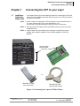
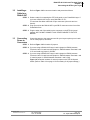
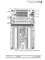
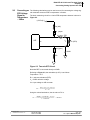
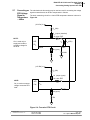
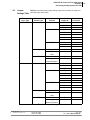
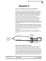
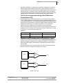
27 Renmar Avenue
Walpole, MA 02081
Web site: www.ueidaq.com
E-mail: [email protected]
Tel: 508-921-4600
FAX: 508-668-2350
PowerDNA STP-AI-U
Universal Analog Input
Screw
Terminal Panel
—
User Manual
November 2007 Edition
PN Man-DNA-STP-AI-U-1107
Version 1.5
© Copyright 1998-2007 United Electronic Industries, Inc. All rights reserved.
DNA-STP-AI-U User Manual
No part of this publication may be reproduced, stored in a retrieval system, or transmitted, in any form
by any means, electronic, mechanical, by photocopying, recording, or otherwise without prior written
permission.
Information furnished in this manual is believed to be accurate and reliable. However, no responsibility
is assumed for its use, or for any infringement of patents or other rights of third parties that may result
from its use.
All product names listed are trademarks or trade names of their respective companies.
See the UEI website for complete terms and conditions of sale:
http://www.ueidaq.com/company/terms.aspx
Contacting United Electronic Industries
Mailing Address:
27 Renmar Avenue
Walpole, MA 02081
U.S.A.
For a list of our distributors and partners in the US and around the world, please see
http://www.ueidaq.com/partners/
Support:
Telephone:
Fax:
(508) 921-4600
(508) 668-2350
Also see the FAQs and online “Live Help” feature on our web site.
Internet Support:
Support:
Web-Site:
FTP Site:
[email protected]
www.ueidaq.com
ftp://ftp.ueidaq.com
Product Disclaimer:
WARNING!
DO NOT USE PRODUCTS SOLD BY UNITED ELECTRONIC INDUSTRIES, INC. AS CRITICAL
COMPONENTS IN LIFE SUPPORT DEVICES OR SYSTEMS.
Products sold by United Electronic Industries, Inc. are not authorized for use as critical components in
life support devices or systems. A critical component is any component of a life support device or
system whose failure to perform can be reasonably expected to cause the failure of the life support
device or system, or to affect its safety or effectiveness. Any attempt to purchase any United Electronic
Industries, Inc. product for that purpose is null and void and United Electronic Industries Inc. accepts
no liability whatsoever in contract, tort, or otherwise whether or not resulting from our or our
employees' negligence or failure to detect an improper purchase.
ii
iii
Table of Contents
Chapter 1 Connecting the STP to your Layer . . . . . . . . . . . . . . . . . . . . . . . . . . . . . . . . . . 1
1.1
Installing a Cable for a DNA-AI-225 . . . . . . . . . . . . . . . . . . . . . . . . . . . . . . . . . . . . . . 1
1.2
Installing a Cable for a DNA-AI-207 . . . . . . . . . . . . . . . . . . . . . . . . . . . . . . . . . . . . . . 2
1.3
Connecting Power to Connectors . . . . . . . . . . . . . . . . . . . . . . . . . . . . . . . . . . . . . . . . 2
Chapter 2 Connecting Analog Inputs to the STP . . . . . . . . . . . . . . . . . . . . . . . . . . . . . . . 4
2.1
Overview . . . . . . . . . . . . . . . . . . . . . . . . . . . . . . . . . . . . . . . . . . . . . . . . . . . . . . . . . . . 4
2.2
Connecting Thermocouples . . . . . . . . . . . . . . . . . . . . . . . . . . . . . . . . . . . . . . . . . . . . 4
2.3
Enabling the CJC Feature. . . . . . . . . . . . . . . . . . . . . . . . . . . . . . . . . . . . . . . . . . . . . . 4
2.4
2.4.1
2.4.2
Connecting Voltage Inputs . . . . . . . . . . . . . . . . . . . . . . . . . . . . . . . . . . . . . . . . . . . . . 7
Enabling Filters . . . . . . . . . . . . . . . . . . . . . . . . . . . . . . . . . . . . . . . . . . . . . . . . 7
Enabling Return to Ground Through Resistor . . . . . . . . . . . . . . . . . . . . . . . . . 7
2.5
Connecting RTDs (+5V Excitation) . . . . . . . . . . . . . . . . . . . . . . . . . . . . . . . . . . . . . . . 7
2.6
Converting an RTD Voltage Signal to Temperature – 2-Wire. . . . . . . . . . . . . . . . . . . 8
2.7
Converting an RTD Voltage Signal to Temperature – 4-Wire. . . . . . . . . . . . . . . . . . 10
2.8
Jumper Settings Table . . . . . . . . . . . . . . . . . . . . . . . . . . . . . . . . . . . . . . . . . . . . . . . 12
Appendix A — Thermocouple Measurement Using an AI-225/AI-207. . . . . . . . . . . . . . . . 13
Index
. . . . . . . . . . . . . . . . . . . . . . . . . . . . . . . . . . . . . . . . . . . . . . . . . . . . . . . . . . . . . . . . . . 17
© Copyright 2007
United Electronic Industries, Inc.
Tel: 508-921-4600
Date: 11. 07. 2007
Vers: 1.5
File:dna-stp-ai-u UserManualTOC.fm
iv
List of Figures
Chapter 1 Connecting the STP to your Layer . . . . . . . . . . . . . . . . . . . . . . . . . . . . . . . . . . 1
1-1
Connecting Your Layer to STP-AI-U Panel.................................................................... 1
1-2
Location of Jumpers/Connectors on STP-AI-U Panel.................................................... 3
Chapter 2 Connecting Analog Inputs to the STP . . . . . . . . . . . . . . . . . . . . . . . . . . . . . . . 4
2-1
Block Diagram of DNA-STP-AI-U Panel ........................................................................ 5
2-2
Location of Jumpers and Terminals on STP Panel........................................................ 6
2-3
Two-wire RTD Circuit..................................................................................................... 8
2-4
Four-wire RTD Circuit .................................................................................................. 10
©
© Copyright
Copyright 2007
2007
United
United Electronic
Electronic Industies,
Industries,Inc.
Inc.
Tel: 508-921-4600
Date:11. 07. 2007
Date: 11. 07. 2007
Vers:
Vers:
1.5
1.0
File:dna-stp-ai-u
File:dna-stp-ai-uUserManualLOF.fm
UserManualLOF.fm
DNA-STP-AI-U Universal Terminal Panel
Chapter 1
Connecting the STP to your Layer
Chapter 1
1.1
Connecting the STP to your Layer
Installing a
Cable for a
DNA-AI-225
This chapter defines the recommended procedure for connecting the STP-AI-U
panel to your PowerDNA Layer board. Refer to Figure 2-1 for connector location
and proceed as follows:
STEP 1: Select a cable for connecting the STP-AI-U panel to your PowerDNA Layer. If
you have a DNA-AI-225 Layer, use a DNA-CBL-62 2.5-ft,
62-conductor round cable with 62-pin male connectors on both ends.
STEP 2: Plug one end into the DNA-AI-225 Layer DB-62 connector on the front of the
PowerDNA Cube.
STEP 3: Plug the other end of the cable into the connector on the STP-AI-U panel
marked J225. DO NOT CONNECT ANY OTHER CABLES TO THE STP
BOARD.
Connect cables
between these
connectors
or
DNA-CBL-37 Cable
(Use with AI-207)
DNA-CBL-62 Cable
(Use only with AI-225)
Figure 1-1 Connecting Your Layer to STP-AI-U Panel
© Copyright
Copyright2006
2007
all rights reserved
d ©Electronic
Industries,
Inc.
United
UnitedElectronic
ElectronicIndustries,
Industries,Inc.
Inc.
81-821-2890
Tel: 508-921-4600
www.ueidaq.com
Date: 11.
11.07.
07.2007
Printed
2007 11. 07. 2007
Vers:
Vers:
1.50.5
1.0
File:
File:stp-ai-u
stp-ai-u
ManualChap1.fm
Fax:
ManualChap1.fm
781-821-2891
1
DNA-STP-AI-U Universal Terminal Panel
Chapter 1
Connecting the STP to your Layer
1.2
Installing a
Cable for a
DNA-AI-207
Refer to Figure 1-2 for connector location and proceed as follows:
STEP 1: Select a cable for connecting the STP-AI-U panel to your PowerDNA Layer. If
you have a DNA-AI-207 Layer, use a DNA-CBL-37 3-ft.,
37-conductor flat ribbon cable with 37-pin connectors (one male and one
female).
STEP 2: Plug one end into the DNA-AI-207 Layer DB-37 connector on the front of the
PowerDNA Cube.
STEP 3: Plug the other end of the cable into the connector on the STP-AI-U panel
marked J207. DO NOT CONNECT ANY OTHER CABLES TO THE STP
BOARD.
1.3
Connecting
Power to
Connectors
Connecting power to the connector used for your Layer requires you to install
one or more jumpers, as follows:
STEP 1: Refer to Figure 1-2 for location of jumpers.
STEP 2: If you are using a DNA-AI-225 Layer, install a jumper in JPOW1 between
Terminals 2 and 3. Install a second jumper in JPOW2 between Terminals 2 and
3. Do not install any jumper in JPOW3.
STEP 3: If you are using a DNA-AI-207 Layer, install a jumper in JPOW1 between
Terminals 2 and 3. Install a second jumper in JPOW2 between Terminals 1 and
2. Install a jumper in JPOW3 between terminals 1 and 2 (ON).
Figure 1-2 shows the locations of various jumpers on the STP-AI-U panel
board. (Refer to Table 2-2 on page 12 for a summary of all jumper settings.)
© Copyright
Copyright2006
2007
all rights reserved
d ©Electronic
Industries,
Inc.
United
UnitedElectronic
ElectronicIndustries,
Industries,Inc.
Inc.
81-821-2890
Tel: 508-921-4600
www.ueidaq.com
Date: 11.
11.07.
07.2007
Printed
2007 11. 07. 2007
Vers:
Vers:
1.50.5
1.0
File:
File:stp-ai-u
stp-ai-u
ManualChap1.fm
Fax:
ManualChap1.fm
781-821-2891
2
DNA-STP-AI-U Universal Terminal Panel
Chapter 1
Connecting the STP to your Layer
JPOW3
J225
Connector
JPOW2
J201
JPOW1
Connector
(Legacy)
J207
Connector
Figure 1-2 Location of Jumpers/Connectors on STP-AI-U Panel
© Copyright
Copyright2006
2007
all rights reserved
d ©Electronic
Industries,
Inc.
United
UnitedElectronic
ElectronicIndustries,
Industries,Inc.
Inc.
81-821-2890
Tel: 508-921-4600
www.ueidaq.com
Date: 11.
11.07.
07.2007
Printed
2007 11. 07. 2007
Vers:
Vers:
1.50.5
1.0
File:
File:stp-ai-u
stp-ai-u
ManualChap1.fm
Fax:
ManualChap1.fm
781-821-2891
3
DNA-STP-AI-U Universal Terminal Panel
Chapter 2
Connecting Analog Inputs to the STP
Chapter 2
2.1
2.2
Overview
Connecting
Thermocouples
Connecting Analog Inputs to the STP
This chapter describes the procedures necessary to do the following:
•
Connect analog inputs of various types to the STP-AI-U panel.
•
Insert jumpers on the board to configure the inputs and options for the
types of input signals you are working with. (Refer to Table 2-2 on
page 12.)
•
Define the linearization needed with an RTD input to convert analog
voltage input to temperature.
To connect thermocouple inputs, do the following:
STEP 1: Connect each thermocouple signal line to the corresponding AINx Sig terminal
on TB1 or TB2. Connect each thermocouple return line to the corresponding
AINx Ret terminal on TB1 or TB2. Refer to Figure 2-2 for location of TB1, TB2,
and screw terminals.
STEP 2: To enable open thermocouple detection and low pass filter to ground, insert a
jumper on JDx, where x is the channel number for that thermocouple. This
action connects the signal line of the x channel to the open thermocouple
detector circuit and a filter to ground. The location of JDx jumper terminals is
noted in Figure 2-2.
NOTE: For every thermocouple return line, you should also enable a return to
ground through a filter (jumper JGx), through a 10k resistor (Jumper
Nx), or both. It is sufficient, however, to insert just the Nx jumper
because of the wide difference in resistor values. Inserting both Nx and
JGx jumpers is not necessary, but inserting both will not cause an error.
The location of all jumper terminals is shown in Figure 2-2. (Refer to
Table 2-2 on page 12 for a summary of all jumper settings.)
2.3
Enabling the
CJC Feature
To enable cold junction compensation (CJC) for use with thermocouples, do the
following:
STEP 1: Install jumpers on JTC1 and JTC2, as indicated in Figure 2-2.
This connects the CJC sensor to AIn 24 Sig and Ret lines.
STEP 2: Install jumpers on JD24, N24, and JG24, as indicated in Figure 2-2.
The JD24 jumper connects the Open TC detection/low pass filter feature to the
AIn24 Sig line. The JG24 jumper connects a 10 megohm resistor and low pass
filter to ground on the AIn24 Ret line. The N24 jumper connects a 10 kohm resistor to ground to the AIn24 Return line.
Figure 2-1 is a block diagram of the STP-AI-U panel. Refer to this figure to see
the function of each jumper. (Refer to Table 2-2 on page 12 for a summary of all
jumper settings.)
Copyright 2006
2007
all rights reserved
d ©©
Electronic
Industries,
Inc.
United Electronic Industries, Inc.
81-821-2890
Tel: 508-921-4600
www.ueidaq.com
Date:
Date: 11.
11.07.
07.2007
Printed
2007 11. 07. 2007
Vers:
Vers:1.5
0.5
1.0
File:
File:stp-ai-u
stp-ai-uManualChap2.fm
Fax:
ManualChap2.fm
781-821-2891
4
!'%",!.*,
JTC1
CJC Sensor
JTC2
J207/208
J201/202
J225
DIn1
DIn0
3
21
JPOW1
21
20
1
2
JPOW3
22
AIn24 Ret
N
JG
AIn Sig
P
JD
AIn Ret
#$
Sig
JPOW2
3
DIn2
8
2
JD
#$
Ret
31
Analog Input Signals/Returns
DIn3
26
P
Ret
AIn24 Sig
N
JG
3
'
#*#+!"&#
1:101
)#( #+
AIn
1
Sig
!'%",!.*,
AIn
5V Reference
+VCC -VCC/AGND
DIO_0 DIO_1 DIO_2
+5VRef
DNA-STP-AI-U Universal Terminal Panel
Chapter 2
Connecting Analog Inputs to the STP
Typical Jumper Terminals
(x is channel ID number)
Refer to Figure 2-2 for location on board.
Figure 2-1 Block Diagram of DNA-STP-AI-U Panel
Figure 2-2 shows the locations of jumpers and terminals on the STP board.
Copyright 2006
2007
all rights reserved
d ©©
Electronic
Industries,
Inc.
United Electronic Industries, Inc.
81-821-2890
Tel: 508-921-4600
www.ueidaq.com
Date:
Date: 11.
11.07.
07.2007
Printed
2007 11. 07. 2007
Vers:
Vers:1.5
0.5
1.0
File:
File:stp-ai-u
stp-ai-uManualChap2.fm
Fax:
ManualChap2.fm
781-821-2891
5
DNA-STP-AI-U Universal Terminal Panel
Chapter 2
Connecting Analog Inputs to the STP
Px jumpers
Nx jumpers
N24
JTC2
JG24
JD24
(alternates in
reverse order
down to JG16)
JDx jumpers
JGx jumpers
(alternating
up to JG15)
JTC1
CJC
Channel
TB1
(screw
terminal
block)
TB2
(screw
terminal
block)
Figure 2-2 Location of Jumpers and Terminals on STP Panel
Copyright 2006
2007
all rights reserved
d ©©
Electronic
Industries,
Inc.
United Electronic Industries, Inc.
81-821-2890
Tel: 508-921-4600
www.ueidaq.com
Date:
Date: 11.
11.07.
07.2007
Printed
2007 11. 07. 2007
Vers:
Vers:1.5
0.5
1.0
File:
File:stp-ai-u
stp-ai-uManualChap2.fm
Fax:
ManualChap2.fm
781-821-2891
6
DNA-STP-AI-U Universal Terminal Panel
Chapter 2
Connecting Analog Inputs to the STP
2.4
Connecting
To connect voltage (or millivolt) inputs to the STP, do the following:
Voltage Inputs
STEP 1: Connect each voltage input signal line to a terminal onTB1 or TB2 marked AInx
Sig, where x is the channel number.
STEP 2: Connect each voltage input return line to a terminal onTB1 or TB2 marked AInx
Ret, where x is the channel number.
2.4.1
Enabling
Filters
To enable return to ground through a 10 megohm resistor/low pass filter circuit,
insert jumpers in JGx for each selected channel, where x is the channel number.
The location of JGx jumper terminals is noted in Figure 2-2.
2.4.2
Enabling
Return to
Ground
Through
Resistor
To enable a ground return through a 10 kohm resistor on each voltage input,
insert a jumper on Nx, where x is the channel number. This action connects the
return line of the x channel input to ground through a 10kOhm resistor. The location of Nx jumper terminals is noted in Figure 2-2.
2.5
Connecting
RTDs (+5V
Excitation)
To connect +5VRef excitation to RTD inputs, do the following:
STEP 1: For every RTD input to which you want to connect internal +5V excitation, insert
a jumper in Px, where x is the channel number of the signal line of the RTD input.
The location of Px jumper terminals is noted in Figure 2-2.
NOTE: If you use an external voltage or current excitation source, do not insert
any jumpers in Px, where x is the channel number. Instead, connect
your external source directly to the AInx Sig terminals on TB1 or TB2.
STEP 2: Connect the screw terminal ”RET” to an “AGND” terminal.
Copyright 2006
2007
all rights reserved
d ©©
Electronic
Industries,
Inc.
United Electronic Industries, Inc.
81-821-2890
Tel: 508-921-4600
www.ueidaq.com
Date:
Date: 11.
11.07.
07.2007
Printed
2007 11. 07. 2007
Vers:
Vers:1.5
0.5
1.0
File:
File:stp-ai-u
stp-ai-uManualChap2.fm
Fax:
ManualChap2.fm
781-821-2891
7
DNA-STP-AI-U Universal Terminal Panel
Chapter 2
Connecting Analog Inputs to the STP
2.6
Converting an
RTD Voltage
Signal to
Temperature
– 2-Wire
The following calculations may be used as a tool for converting the voltage signal measured across an RTD to temperature in Celsius.
The basic measuring circuit for a 2-wire RTD temperature detector is shown in
Figure 2-3.
(+5V Ref) Vr
Rs (20k)
Px jumper
22.1ohm SIG
R22.1
A/D
Vm
Vu
Ru (RTD)
RET
Nx (open)
AGND
10k
Figure 2-3 Two-wire RTD Circuit
Note that RET is connected directly to AGND.
Referring to Figure 2-3, the calculation (at 0°C) is as follows:
Temperature = 0 °C
Ru = unknown resistance (RTD)
Vr = 5VDC reference voltage
Vm= input voltage to A/D converter
( R 22.1 + R s ) ⋅ V m – R 22.1 V r
R u = -----------------------------------------------------------------Vr – Vm
Using the values listed above, the the value of Ru is:
20022.1 × 0.0303399 ) – 22.1 ( 5 ) = 100ohms
R u = (-------------------------------------------------------------------------------5 – 0.0303399
Copyright 2006
2007
all rights reserved
d ©©
Electronic
Industries,
Inc.
United Electronic Industries, Inc.
81-821-2890
Tel: 508-921-4600
www.ueidaq.com
Date:
Date: 11.
11.07.
07.2007
Printed
2007 11. 07. 2007
Vers:
Vers:1.5
0.5
1.0
File:
File:stp-ai-u
stp-ai-uManualChap2.fm
Fax:
ManualChap2.fm
781-821-2891
8
DNA-STP-AI-U Universal Terminal Panel
Chapter 2
Connecting Analog Inputs to the STP
Using a standard DIN 100 ohm Pt RTD with an alpha of
0.00385 ohms/°C yields the values shown in Table 2-1.
Temperature
°C
Ru
Vm
V22.1
Vu
Ohms
mV
mV
mV
CURRENT
mA
-200
18.52
10.134
5.5739
4.6204
.24950
-100
60.25
20.503
5.5025
14.990
.24879
0
100.0
30.339
5.4914
24.848
.24848
100
138.50
39.831
5.4808
34.348
.24800
200
175.86
49.005
5.4709
43.5341
.24755
300
212.05
57.861
5.4611
52.3997
.24711
400
247.09
65.902
5.4494
60.9275
.24658
500
280.98
74.639
5.4427
69.1997
.24628
Table 2-1 Vin vs. RTD Resistance at Various Temperatures
Copyright 2006
2007
all rights reserved
d ©©
Electronic
Industries,
Inc.
United Electronic Industries, Inc.
81-821-2890
Tel: 508-921-4600
www.ueidaq.com
Date:
Date: 11.
11.07.
07.2007
Printed
2007 11. 07. 2007
Vers:
Vers:1.5
0.5
1.0
File:
File:stp-ai-u
stp-ai-uManualChap2.fm
Fax:
ManualChap2.fm
781-821-2891
9
DNA-STP-AI-U Universal Terminal Panel
Chapter 2
Connecting Analog Inputs to the STP
2.7
Converting an
RTD Voltage
Signal to
Temperature
– 4-Wire
The calculations in this section may be used as a tool for converting the voltage
signal measured across an RTD to temperature in Celsius.
The basic measuring circuit for a 4-wire RTD temperature detector is shown in
Figure 2-4.
(+5V Ref) Vr
Rs (20k)
Px jumper (installed)
22.1ohm SIG
NOTE:
Chx is used only to
supply and read the
excitation voltage for
the RTD.
R22.1
A/D
Vu
Ru (RTD)
Chx
RET
AGND
Nx (open)
AGND
(+5V Ref) Vr
Rs (20k)
Px jumper (open)
22.1ohm SIG
NOTE:
Chy is used to measure
voltage across the RTD
itself..
A/D
Chy
R22.1
Vm
RET
Nx (open)
10k
Figure 2-4 Four-wire RTD Circuit
Copyright 2006
2007
all rights reserved
d ©©
Electronic
Industries,
Inc.
United Electronic Industries, Inc.
81-821-2890
Tel: 508-921-4600
www.ueidaq.com
Date:
Date: 11.
11.07.
07.2007
Printed
2007 11. 07. 2007
Vers:
Vers:1.5
0.5
1.0
File:
File:stp-ai-u
stp-ai-uManualChap2.fm
Fax:
ManualChap2.fm
781-821-2891
10
DNA-STP-AI-U Universal Terminal Panel
Chapter 2
Connecting Analog Inputs to the STP
As shown in the diagram, Channel x supplies and reads the excitation voltage
for the 4-wire RTD circuit. Channel y reads the voltage across the RTD itself.
Also note that RET is connected to AGND.
The calculation for determining the RTD resistance for Channel y is:
( R s + R 22.1 ) ⋅ V m
Ru = ----------------------------------------Vr – Vm
The table below lists the calculation results at various temperatures.
Copyright 2006
2007
all rights reserved
d ©©
Electronic
Industries,
Inc.
United Electronic Industries, Inc.
81-821-2890
Temperature
°C
Ohms
-200
18.52
4.62376
-100
60.31
15.04219
0
100.00
24.96663
100
138.50
34.57883
200
175.86
43.90573
300
212.05
52.94103
400
247.09
61.68922
500
280.98
70.15030
Tel: 508-921-4600
www.ueidaq.com
Date:
Date: 11.
11.07.
07.2007
Printed
2007 11. 07. 2007
Ru
Vm
mV
Vers:
Vers:1.5
0.5
1.0
File:
File:stp-ai-u
stp-ai-uManualChap2.fm
Fax:
ManualChap2.fm
781-821-2891
11
DNA-STP-AI-U Universal Terminal Panel
Chapter 2
Connecting Analog Inputs to the STP
2.8
Jumper
Table 2-2 summarizes the jumper settings required for selection of options for
Settings Table each layer type and function.
Layer Type
Sensor Type
Function
Jumper ID
Terminals
Connected
DNA-AI-207
Thermocouples
Power
JPOW1
2-3
JPOW2
1-2
JPOW3
1-2
JTC1
ON
JTC2
ON
JD24
ON
N24
ON
JG24
ON
JDX
ON
JGx
--
Nx
ON
10k Return to GND
Nx
ON
1 MΩ + Filter to
GND
JGx
--
+5V Internal Excit.
Px
ON
User-supplied
Extern Excitation
Px
Open
Power
JPOW1
2-3
JPOW2
2-3
JPOW3
Open
JTC1
ON
JTC2
ON
JD24
ON
N24
ON
JG24
ON
JDX
ON
JGx
--
Nx
ON
10k Return to GND
Nx
ON
1 MΩ + Filter to
GND
JGx
--
+5V Int Exc.
Px
ON
User-supplied
External Excitation
Px
Open
Enable CJC
Open TC Detect.
Voltage
RTD
DNA-AI-225
Thermocouples
Enable CJC
Open TC Detect.
Voltage
RTD
Table 2-2 Jumper Settings Table
Copyright 2006
2007
all rights reserved
d ©©
Electronic
Industries,
Inc.
United Electronic Industries, Inc.
81-821-2890
Tel: 508-921-4600
www.ueidaq.com
Date:
Date: 11.
11.07.
07.2007
Printed
2007 11. 07. 2007
Vers:
Vers:1.5
0.5
1.0
File:
File:stp-ai-u
stp-ai-uManualChap2.fm
Fax:
ManualChap2.fm
781-821-2891
12
DNA-STP-AI-U Universal Terminal Panel
Appendix A
Thermocouple Measurement Using an AI-225/AI-207
A thermocouple is a sensor used to measure temperature in a wide range of
applications. Its ability to sense temperature is based on the so-called “Seebeck
Effect”, discovered by Thomas Seebeck in 1821. The Seebeck Effect, also
known as the thermoelectric effect, states that any electrical conductor will
produce a voltage when subjected to a thermal gradient. The magnitude and
polarity of the voltage produced varies with the type of metal used for the
conductor and the magnitude and polarity of the thermal gradient.
A thermocouple is constructed by connecting two conductors, composed of
dissimilar metals, at both ends to form two junctions. Since the second
conductor senses the same thermal gradient as the first, it also produces a
voltage. This voltage, however, is different from that of the first conductor
because it is made from a different metal. The small difference between the two
voltages, which is typically in the millivolt range, is used for measurement of the
thermal gradient.
Since the voltage is generated by a thermal difference between the junctions,
one junction is called the “hot junction” and the other is called the “cold junction”
or “reference junction.” An increase in the temperature difference between hot
and cold junctions increases the voltage generated in a non-linear relation. The
degree of linearity is a property of the two metals used to make the
thermocouple.
Breaking the circuit to insert a voltmeter as shown in the diagram below
illustrates how a thermocouple is typically used to measure temperature in an
application.
wire of metal A
“hot” junction
at point of
temperature
sensing
“cold” junction
at ambient
temperature
Metal C
wire of metal B
Metal C
Isothermal
Block
T
Voltmeter
cold junction
temperature
measurement
Cold Junction Compensation Theory
Typically, a voltage is produced by a thermocouple at any given temperature.
For example, the K-type thermocouple at 300°C will produce 12.2mV. To
measure this voltage accurately, you must compensate for using any contact
made to a thermocouple -- a technique called cold junction compensation (CJC).
In case you are wondering why connecting a voltmeter to a thermocouple does
not make several additional thermocouple junctions (leads connecting to the
thermocouple, leads to the meter, inside the meter etc), the law of intermediate
metals states that a third metal, inserted between the two dissimilar metals of a
thermocouple junction will have no effect provided that the two junctions are at
Copyright 2006
2007
all rights reserved
d ©©
Electronic
Industries,
Inc.
United Electronic Industries, Inc.
81-821-2890
Tel: 508-921-4600
www.ueidaq.com
Date:
Date: 11.
11.07.
07.2007
Printed
2007 11. 07. 2007
Vers:
Vers:1.5
0.5
1.0
File:
File:dna-stp-ai-uAppA.fm
dna-stp-ai-uAppA.fm
Fax: 781-821-2891
13
DNA-STP-AI-U Universal Terminal Panel
the same temperature. It is important to keep this in mind when we construct
thermocouple junctions. Based on this law, it is quite acceptable to make a
thermocouple junction by soldering the two metals together as the solder will not
affect the reading. In practice, however, thermocouple junctions are made by
welding the two metals together (usually by capacitive discharge) because this
ensures that the performance is not limited by the melting point of solder.
Cold Junction Compensation Using a PowerDNA Screw
Terminal Panel (STP)
Ambient temperature measurement is done by Cold Junction compensation
(CJC). A PowerDNA Screw Terminal Panel has an isothermal metal block which
is at ambient temperature. The voltage generated by the ambient temperature is
measured using a dedicated CJC channel available in UEI Analog Input Layers.
Software then determines the voltage created at the “cold” junction and
subtracts this error voltage before linearizing the thermocouple input.
Table A-1 describes the CJC channel number for various Analog Input Layers using
a DNA-STP-AI-U or a DNA-AI-207TC Screw Terminal Panel. Note, however, that the
STP-AI-207TC is not used with the AI-225 Layer.
Table A-1.
Layer
CJC channel Number
Comments
AI-207
Channel 33
Single-Ended
AI-225
Channel 24
Single-Ended
Hardware Setup of Analog Input AI-225 and AI-207 Layers
Analog Input AI-225 and AI-207 Layers have a dedicated CJC channel which
measures voltage corresponding to the ambient temperature. The example
below shows the hardware set to measure temperatures accurately using a
thermocouple.
The thermocouple input is connected to the one of the Analog Input channels
and the CJC input is configured in software as per Table 1.
AIn0
ADC
Vtc
CJC
ADC
Vcjc
Vresult = Vtc + Vcjc
Copyright 2006
2007
all rights reserved
d ©©
Electronic
Industries,
Inc.
United Electronic Industries, Inc.
81-821-2890
Tel: 508-921-4600
www.ueidaq.com
Date:
Date: 11.
11.07.
07.2007
Printed
2007 11. 07. 2007
Vers:
Vers:1.5
0.5
1.0
File:
File:dna-stp-ai-uAppA.fm
dna-stp-ai-uAppA.fm
Fax: 781-821-2891
14
DNA-STP-AI-U Universal Terminal Panel
Linearization
Within the "usable" temperature range of any thermocouple, there is a
proportional relationship between thermocouple voltage and temperature. This
relationship, however, is by no means a linear relationship. In fact, most
thermocouples are extremely non-linear over their operating ranges. To obtain
temperature data from a thermocouple, it is necessary to convert the non-linear
thermocouple voltage to temperature units. This process is called "linearization."
Several methods are commonly used to linearize thermocouples. At the lowcost end of the solution spectrum, one can restrict the thermocouple operating
range such that the thermocouple is nearly linear to within the measurement
resolution. At the opposite end of the spectrum, special thermocouple interface
components (integrated circuits or modules) are available to perform both
linearization and reference junction compensation in the analog domain. In
general, neither of these methods is well-suited for cost-effective, multipoint data
acquisition systems.
In addition to linearizing thermocouples in the analog domain, it is possible to
perform such linearizations in the digital domain. This is accomplished by means
of either piece-wise linear approximations (using look-up tables) or arithmetic
approximations, or in some cases, a hybrid of these two methods.
Software Implementation
To do accurate temperature measurements, one has to read the channel where
the thermocouple is connected, as well as a CJC channel. Feed these values to
a NIST-derived polynomial formula to get an accurate thermocouple junction
temperature.
Code Snippet for the AI-225:
To read the CJC channel, you must specify Channel 24 in single-ended mode in
the channel list. The snippet of the code is shown below:
for (i = 0; i < CHANNELS; i++) {
cl[i] = i |DQ_LNCL_GAIN(DQ_AI225_GAIN_1) } DQ_LNCL_DIFF;
}
c1[CHANNELS] = 24 | DQ_LNCL_GAIN(DQ_AI225_GAIN_1);
Code Snippet for the AI-207:
To read the CJC channel, you must specify Channel 33 in single-ended mode in
the channel list. The snippet of the code is shown below:
for (i = 0; i < CHANNELS; i++) {
cl[i] = i |DQ_LNCL_GAIN(DQ_AI207_GAIN_1) } DQ_LNCL_DIFF;
}
c1[CHANNELS] = 33 | DQ_LNCL_GAIN(DQ_AI207_GAIN_1);
Open TC Detection:
A DNA-STP-AI-U Screw Terminal Panel has the hardware implementation to
detect an open TC. An Open TC will show high positive temperatures beyond
the limits of the thermocouple range.
Copyright 2006
2007
all rights reserved
d ©©
Electronic
Industries,
Inc.
United Electronic Industries, Inc.
81-821-2890
Tel: 508-921-4600
www.ueidaq.com
Date:
Date: 11.
11.07.
07.2007
Printed
2007 11. 07. 2007
Vers:
Vers:1.5
0.5
1.0
File:
File:dna-stp-ai-uAppA.fm
dna-stp-ai-uAppA.fm
Fax: 781-821-2891
15
DNA-STP-AI-U Universal Terminal Panel
References:
Copyright 2006
2007
all rights reserved
d ©©
Electronic
Industries,
Inc.
United Electronic Industries, Inc.
81-821-2890
•
DNA-AI-225 User Manual
•
DNA-AI-207 User Manual
•
DNA-STP-AI-U User Manual
Tel: 508-921-4600
www.ueidaq.com
Date:
Date: 11.
11.07.
07.2007
Printed
2007 11. 07. 2007
Vers:
Vers:1.5
0.5
1.0
File:
File:dna-stp-ai-uAppA.fm
dna-stp-ai-uAppA.fm
Fax: 781-821-2891
16
Index
17
Index
Numerics
2-wire RTD 8
4-wire RTD 10
B
Enabling open TC detection/low pass filters
I
Installing a Cable for a DNA-AI-207 2
Installing a Cable for a DNA-AI-225 1
Block Diagram of DNA-STP-AI-U Panel
C
5
DNA-CBL-37
DNA-CBL-62
E
J
Jumper Location
Connecting Power to Connectors 2
Connecting RTDs (+5V Excitation) 7
Connecting thermocouple inputs 4
Connecting voltage inputs 7
Converting an RTD voltage signal to temperature 8,
10
D
2
1
L
2
Location of Jumpers and Terminals on STP Panel 6
S
Support ii
Support email
[email protected]
Support FTP Site
ftp
ii
//ftp.ueidaq.com ii
Enabling cold junction compensation
©©Copyright
Copyright2006
2007all rights reserved
United
UnitedElectronic
ElectronicIndustries,
Industries,Inc.
Inc.
4
4
Tel: 508-921-4600
Date:
Date: 11.
11.07.
07.2007
2007
Support Web Site
www.ueidaq.com
ii
Vers:
Vers: 1.5
1.0
File:dna-stp-ai-u
File:dna-stp-ai-uUserManualIX.fm
UserManu-