1
Modbus® RTU Serial Communications
User Manual
51-52-25-66M
10/04
Industrial Measurement & Control
Copyright, Notices, and Trademarks
Printed in U.S.A. – © Copyright 2004 by Honeywell
Revision M – 11/04
Warranty/Remedy
Honeywell warrants goods of its manufacture as being free of defective materials and faulty
workmanship. Contact your local sales office for warranty information. If warranted goods are
returned to Honeywell during the period of coverage, Honeywell will repair or replace without charge
those items it finds defective. The foregoing is Buyer's sole remedy and is in lieu of all other
warranties, expressed or implied, including those of merchantability and fitness for a particular
purpose. Specifications may change without notice. The information we supply is believed to be
accurate and reliable as of this printing. However, we assume no responsibility for its use.
While we provide application assistance personally, through our literature and the Honeywell web
site, it is up to the customer to determine the suitability of the product in the application.
Industrial Measurement & Control
Honeywell
1100 Virginia Drive
Fort Washington, PA 19034
Modbus is a registered trademark of MODICON, Inc.
Windows is an addressed trademark of Microsoft Inc.
The omission of a name from this list is not to be interpreted that the name is not a trademark.
Reference: Modicon Modbus Protocol Reference Guide - PI-MBUS-300 Rev. G
ii
Modbus® RTU Serial Communications User Manual
10/04
About This Document
Abstract
This document provides generic information for Honeywell instruments implementing the Modbus RTU Serial
Communications protocol. Configuration information relating to specific devices is supplied in separate user
manuals. Refer to 1.2 Modbus RTU Configuration Interface for a list of instruments and the corresponding
configuration interface user manuals.
Contacts
World Wide Web
The following lists Honeywell’s World Wide Web sites that will be of interest to our customers.
Honeywell Organization
WWW Address (URL)
Corporate
http://www.honeywell.com
Industrial Measurement & Control
http://www.honeywell.com/imc
Telephone
Contact us by telephone at the numbers listed below.
Organization
United States and Canada
10/04
Honeywell
Phone Number
1-800-423-9883
1-800-525-7439
Modbus® RTU Serial Communications User Manual
Tech. Support
Service
iii
Contents
1.
INTRODUCTION ................................................................................................... 1
1.1
Modbus RTU Implementation........................................................................................................ 1
1.2
Modbus RTU Configuration Interface ........................................................................................... 1
2.
MODBUS RTU MESSAGE FORMAT ................................................................... 2
2.1
Modbus RTU Link Layer ............................................................................................................... 2
2.2
Modbus RTU Data Layer ............................................................................................................... 3
2.3
IEEE 32-bit Floating-Point Register Information .......................................................................... 4
3.
MODBUS RTU FUNCTION CODES ..................................................................... 9
3.1
Function Code 01 – Read Digital Output Status .......................................................................... 13
3.2
Function Code 02 – Read Digital Input Status............................................................................. 15
3.3
Function Codes 03/04 – Read Input Registers ............................................................................. 16
3.4
Function Code 05 – Force Single Digital Output......................................................................... 18
3.5
Function Codes 06 – Preset Single Register................................................................................. 19
3.6
Function Code 08 – Loopback Message ...................................................................................... 20
3.7
Function Codes 16 (10h) – Preset Multiple Registers.................................................................. 21
3.8
Function Code 17 (11h) – Report Device ID ............................................................................... 22
4.
MODBUS RTU EXCEPTION CODES ................................................................. 25
A.
APPENDIX: REGISTER MAP............................................................................. 27
iv
A.1
Register Map Overview ............................................................................................................ 27
A.2
Miscellaneous Register Map..................................................................................................... 29
A.2.1 RSX, VPR, VRX, UDC5300 Miscellaneous Register Map ............................................. 29
A.2.2 DR4300, DR4500 Chart Record Map ............................................................................... 30
A.3
Loop Value Integer Register Map............................................................................................. 31
A.4
Loop Value Register Map......................................................................................................... 34
A.5
Analog Input Value Register Map ............................................................................................ 37
A.6
Communication or Constant Value Register Map .................................................................... 38
A.7
Math, Calculated Value, or Variable Register Map.................................................................. 39
A.8
Math or Calculated Value Status Register Map........................................................................ 40
A.9
Totalizer Value Register Map................................................................................................... 41
A.10
Totalizer Status Register Map................................................................................................... 42
A.11
Shed Timer Reset Register........................................................................................................ 43
A.12
Maintenance (HealthWatch) Value Register Map .................................................................... 44
A.13
Time Register Map ................................................................................................................... 45
Modbus® RTU Serial Communications User Manual
10/04
A.14
Alarm Status Register Map....................................................................................................... 46
A.15
Alarm Set Point Value Register Map........................................................................................ 47
A.16
Set Point Programmer Value Register Map.............................................................................. 48
A.17
Set Point Programmer Additional Values Register Map .......................................................... 50
A.18 Set Point Programmer Segment Map........................................................................................ 52
A.18.1
Segment Register Map ................................................................................................... 53
A.18.2
Example For Determining a Segment Register.............................................................. 54
A.19
Herculine Smart Actuator Value Register Map ........................................................................ 55
A.20
Herculine Smart Actuator Factory Data Register Map ............................................................. 57
A.21
Herculine Smart Actuator Maintenance Data Register Map..................................................... 58
B.
10/04
APPENDIX: CRC-16 CALCULATION ................................................................ 59
Modbus® RTU Serial Communications User Manual
v
Tables
Table 1-1 Communication and Configuration User Manuals __________________________________ 1
Table 2-1 Modbus RTU Message Formats ________________________________________________ 2
Table 2-2 IEEE Floating Point Number Examples in FP B Format _____________________________ 8
Table 3-1 Modbus RTU Function Codes Definitions ________________________________________ 9
Table 3-2 Maximum Number of Object Addresses for Each Instrument Type – Part 1 _____________ 10
Table 3-3 Maximum Number of Registers Allowable per Request_____________________________ 12
Table 3-4 Request Delay Time* _______________________________________________________ 12
Table 3-5 DR4500 Digital Output Mapping ______________________________________________ 14
Table 3-6 UDC2300/UDC2500/UDC3200/UDC3300 DO Mapping ___________________________ 14
Table 3-7 Herculine Smart Actuators Digital Output Mapping________________________________ 14
Table 4-1 Modbus RTU Data Layer Status Exception Codes _________________________________ 26
Table A-1 Global Register Map________________________________________________________ 27
Figures
Figure 2-1 IEEE Floating-Point Data format _______________________________________________ 4
Figure 2-2 IEEE Floating Point Formats __________________________________________________ 8
vi
Modbus® RTU Serial Communications User Manual
10/04
Introduction
1. Introduction
1.1
Modbus RTU Implementation
This implementation is designed to provide a popular data exchange format connecting these instruments
to both Honeywell and foreign master devices. The Modbus RTU allows the instrument to be a citizen on a
data link shared with other devices that subscribe to the Modbus RTU RS-485 specification.
These instruments DO NOT emulate any MODICON type device. The Modbus RTU specification is
respected in the physical and data link layers. The message structure of the Modbus RTU function codes is
employed and standard IEEE 32-bit floating point and integer formats are used. Data register mapping is
unique to these instruments. The definition in Table 2-1 is the register mapping for many Honeywell
instruments and the corresponding parameter value within those instruments.
1.2
Modbus RTU Configuration Interface
This user manual does not include the configuration interfaces for the instruments supporting the Modbus
RTU Protocol. The following table describes the references to the specific instrument’s communication
and configuration user manuals.
Table 1-1 Communication and Configuration User Manuals
Instrument Model
User Manual Part Number
RSX, VPR, VRX, UDC5300
51-52-25-68
Minitrend V5, Multitrend Plus
V5
43-TV-25-08 Communications Manual
eZtrend V5
43-TV-25-08 Communications Manual V5 (Modbus TCP/IP only)
DR4300
51-52-25-71
DR4500
51-52-25-69
UDC2300
51-52-25-75
UDC3300
51-52-25-70
51-52-25-38 UDC3000A Modbus 485 RTU Communications Manual
DPR100
US1I-6149 DPR100C-DPR100D Communication Option Manual
DPR180/DPR250
EN1I-6189 DPR180/DPR250 Communication Option Manual
10260S/11280S/
SA201/SA2002
51-52-25-103 Modbus Configuration Interface for Herculine Actuators
UDC2500
51-52-25-127
UDC2500 Limit Controller
51-52-25-118
UDC3200
51-52-25-119
UDC3500
51-52-25-120
10/04
Modbus® RTU Serial Communications User Manual
1
Modbus RTU Message Format
2. Modbus RTU Message Format
Table 2-1 Modbus RTU Message Formats
Coding system
8 bit binary
Number of data bits per
character
10 Bits
start bits - 1
data bits - 8
parity bits - 0
stop bits - 1
Parity
Not used
Bit transfer rate
300, 600, 1200, 2400, 4800, 9600, 19200, 38400 Selectable
NOTE: Not all instruments support all Baud Rates.
Duplex
Half duplex Transceiver or TX/RX
Error checking
CRC (cyclic redundancy check)
Polynomial
(CRC-16 10100000000001)
Bit transfer order
LSB first
End of message
Idle line for 3.5 or more characters (>1.82 msec for 19200).
2.1
Modbus RTU Link Layer
The link layer includes the following properties/behaviors:
Slave address recognition,
Start / End of Frame detection,
CRC-16 generation / checking,
Transmit / receive message time-out,
Buffer overflow detection,
Framing error detection,
Idle line detection.
Errors detected by the physical layer in messages received by the slave are ignored and the physical layer
automatically restarts by initiating a new receive on the next idle line detection.
2
Modbus® RTU Serial Communications User Manual
10/04
Modbus RTU Message Format
General Modbus RTU message format
Query message format
[Slave Address, Function Code, Function code dependent data, CRC 16]
Response message format
[Slave Address, Function Code*, Function code dependent data, CRC 16]
* If an error is detected in a valid message the response function code is modified by adding 80 (hex) and the
function code dependent data is replaced by an exception response code as described in Section 4 - Modbus RTU
Exception Codes.
Between messages, the RS-485 link is in a high impedance state. During this time receiving devices are
more susceptible to noise generated false start of messages. Although noise-generated messages are
rejected due to address, framing, and CRC checking, they can cause the loss of a good message when they
are included in the message stream. In the slave, the transmitting device enables its transmitter line driver
and forces an idle line state onto the link for three character time slots prior to transmitting. This action
forces termination of any noise generated messages and improves message frame synchronization.
2.2
Modbus RTU Data Layer
The data layer includes:
•
Diagnostic loopback,
•
Function code recognition / rejection,
•
Busy / repoll,
• Data error code generation
Errors detected by the data layer are rejected and the slave responds to the polling device with a Modbustype status exception error. A summary of the Modbus status exception codes is listed in
Section 4 - Modbus RTU Exception Codes
10/04
Modbus® RTU Serial Communications User Manual
3
Modbus RTU Message Format
2.3
IEEE 32-bit Floating-Point Register Information
The Modbus applications support IEEE 32-bit floating-point information for several of the function codes.
IEEE Floating-Point Data Format
The formula for calculating the floating-point number is:
mantissa x 2
(exponent -127)
(23 bit signed binary with 8 bit biased binary exponent)
byte 4
byte 3
3
2 2
1
1
4 3
6
xxxxxxxx x.xxxxxxx
byte 2
1
5
8
xxxxxxxx
byte 1
7
0
xxxxxxx
mantissa (23 bits)
implied binary point for mantissa
exponent (8 bit unsigned value)
sign of the mantissa 0 = positive, 1 = negative
Figure 2-1 IEEE Floating-Point Data format
Mantissa and Sign
The mantissa is defined by a sign bit (31), and a 23-bit binary fraction. This binary fraction is combined
with an “implied” value of 1 to create a mantissa value, which is greater than or equal to 1.0 and less than
2.0.
The mantissa is positive if the sign bit is zero (reset), and negative if the sign bit is one (set). For example:
DECIMAL
HEXADECIMAL
BINARY
100
42C80000
01000010 11001000 00000000 00000000
The sign bit (31) is zero, indicating a positive mantissa. Removing the sign bits and exponent bits, the
mantissa becomes:
HEXADECIMAL
BINARY
480000
xxxxxxxx x1001000 00000000 00000000
Add an “implied” value of one to the left of the binary point:
BINARY
1.1001000 00000000 00000000
Using positioned notation, this binary number is equal to:
10
. + (1x2 -1 ) + (0x2 -2 ) + (0x2 -3 ) + (1x2 -4 ) = 10
. + 0.5 + 0.0 + 0.0 + 0.0625 = 15625
.
4
Modbus® RTU Serial Communications User Manual
10/04
Modbus RTU Message Format
Exponent
The exponent is defined by an unsigned 8-bit binary value (bits 23 through 30). The value of the exponent
is derived by performing a signed subtraction of 127 (decimal) from the 8-bit exponent value.
DECIMAL
HEXADECIMAL
BINARY
100
42C80000
01000010 11001000 00000000 00000000
removing the sign and mantissa bits, the exponent becomes:
DECIMAL
HEXADECIMAL
BINARY
133
85
x1000010 1xxxxxxx xxxxxxxx xxxxxxxx
or:
1x2 7 + 0x2 6 + 0x2 5 + 0x2 4 + 0x2 3 + 1x2 2 + 0x2 1 + 1x2 0
Subtract a bias of 127 (decimal) from the exponent to determine its value: 133 – 127 = 6.
Mantissa and Exponent Combination
Combining the mantissa and exponent from the two previous examples:
float number = mantissa x 2 exponent
.
float number = 1.5625 x 2 6 = 15625
x 64 = 100.0
Below is a list of sample float values in IEEE format:
DECIMAL
10/04
HEXADECIMAL
100.0
42C80000
-100.0
C2C80000
0.5
3F000000
-1.75
BFE00000
0.0625
3D800000
1.0
3F800000
0.0
00000000
2.0
40000000
55.32
425047AE
Modbus® RTU Serial Communications User Manual
5
Modbus RTU Message Format
Reserved Operands
Per the Standard certain exceptional forms of floating-point operands are excluded from the numbering
system. These are as follows:
EXCEPTION
EXPONENT
MANTISSA
+/- Infinity
All 1’s
All 0’s
Not-a-Number (NAN)
All 1’s
Other than 0’s
Denormalized Number
All 0’s
Other than 0’s
Zero
All 0’s
All 0’s
Modbus Double Register Format
Each IEEE 32-bit floating point number requires two consecutive registers (four bytes) starting with the
register defined as the starting register for the information. The stuffing order of the bytes into the two
registers differs among Modbus hosts. The selections are:
Selection
Description
Byte order
(See Figure
2-1)
FP B
Floating Point Big Endian Format
4, 3, 2, 1
FP BB
Floating Point Big Endian with
byte-swapped
3, 4, 1, 2
FP L
Floating Point Little Endian Format
1, 2, 3, 4
FP LB
Floating Point Little Endian with
byte-swapped
2, 1, 4, 3
Notes
Modicon and
Wonderware
standard
See IEEE Formats starting on next page.
6
Modbus® RTU Serial Communications User Manual
10/04
Modbus RTU Message Format
IEEE Floating Point Formats
FP B - Floating Point Big Endian Format:
Bit 0
Bit 31
M7 M6 M5 M4 M3 M2 M1 M0
E0 M22 M21M20 M19 M18 M17 M16
M15 M14 M13 M12 M11 M10 M9 M8
S E7 E6 E5 E4 E3 E2 E1
High
Low
High
Low
REGISTER N+1
(Low)
REGISTER N
(High)
S=Sign E=Exponent M=Mantissa
FP BB - Floating Point Big Endian with Byte Swapped Format:
Bit 24
Bit 31
Bit 15
S E7 E6 E5 E4 E3 E2 E1
Bit 16
Bit 23
M15 M14 M13 M12 M11 M10 M9 M8
Bit 7
Bit 0
M7 M6 M5 M4 M3 M2 M1 M0
E0 M22 M21M20 M19 M18 M17 M16
High
Bit 8
Low
High
Low
REGISTER N+1
(Low)
REGISTER N
(High)
S=Sign E=Exponent M=Mantissa
continued next page
10/04
Modbus® RTU Serial Communications User Manual
7
Modbus RTU Message Format
FP L - Floating Point Little Endian Format:
Bit 15
Bit 8
S E7 E6 E5 E4 E3 E2 E1
M15 M14 M13 M12 M11 M10 M9 M8
Bit 7
E0 M22 M21M20 M19 M18 M17 M16
M7 M6 M5 M4 M3 M2 M1 M0
High
Bit 16
Bit 23
Bit 0
Bit 24
Bit 31
Low
High
Low
REGISTER N+1
(Low)
REGISTER N
(High)
S=Sign E=Exponent M=Mantissa
FP LB - Floating Point Little Endian with Byte Swapped Format:
Bit 7
M7 M6 M5 M4 M3 M2 M1 M0
Bit 15
Bit 8
E0 M22 M21M20 M19 M18 M17 M16
Bit 24
Bit 31
S E7 E6 E5 E4 E3 E2 E1
M15 M14 M13 M12 M11 M10 M9 M8
High
Bit 16
Bit 23
Bit 0
Low
High
Low
REGISTER N+1
(Low)
REGISTER N
(High)
S=Sign E=Exponent M=Mantissa
Figure 2-2 IEEE Floating Point Formats
Table 2-2 IEEE Floating Point Number Examples in FP B Format
8
IEEE FP B
Register N
Register N+1
Value
(decimal)
MSB LSB
100.0
42C80000h
42h
C8h
00h
00h
55.32
425D47AEh
42h
5Dh
47h
AEh
2.0
40000000h
40h
00h
00h
00h
1.0
3F800000h
3Fh
80h
00h
00h
-1.0
BF800000h
BFh
80h
00h
00h
high
low
high
low
Modbus® RTU Serial Communications User Manual
10/04
Modbus RTU Function Codes
3. Modbus RTU Function Codes
The Honeywell Universal Modbus RTU protocol uses a subset of the standard Modbus RTU function codes
to provide access to process-related information. Several MODICON function codes are employed. It is
appropriate to define instrument-specific "user-defined" function codes. Several standard Modbus RTU
function codes are supported. These standard function codes provide basic support for IEEE 32-bit floating
point numbers and 16-bit integer register representation of instrument’s process data.
Repolling of data is not supported by these instruments.
Table 3-1 Modbus RTU Function Codes Definitions
Function Code
Name
Usage
01
Read Coil Status
Read the State of a Digital Output
02
Read Input Status
Read the State of a Digital Input
03
Read Holding Registers /
04
Read Input Registers
Read Data in 16 bit Register Format (high/low). Used to
read integer or floating point process data. Registers
are consecutive and are imaged from the instrument to
the host.
05
Force Single Coil
Write data to force Digital Output ON/OFF
Values of FF 00 forces DO ON
Values of 00 00 forces DO OFF
Values of FF FF releases the force of the DO
All other values are illegal and will not effect the DO.
RSX, VPR, VRX, UDC5300 ONLY
06
Preset Single Register
Write Data in 16-bit Integer Format (high/low) ONLY.
08
Loopback Test
Used for diagnostic testing of the communications port.
16 (10h)
Preset Multiple Registers
Write Data in 16-bit Format (high/low). Used to write
integer and floating point override data. Registers are
consecutive and are imaged from the host to the
instrument.
17 (11h)
Report Device ID
Read instrument ID and connection information, ROM
version, etc.
20 (14h)
Read General Reference
Used to Read or upload the instrument’s configuration
into the host device. See Section 1.2 - Modbus RTU
Configuration Interface for a reference to the User
Manual for the specific instrument.
21 (15h)
Write General Reference
Used to Write or download an instrument’s
configuration into the instrument from a host device.
See Section 1.2 - Modbus RTU Configuration Interface
for a reference to the User Manual for the specific
instrument.
10/04
Modbus® RTU Serial Communications User Manual
9
Modbus RTU Function Codes
Table 3-2 Maximum Number of Object Addresses for Each Instrument Type
Part 1
RSX
VRX100
VRX150
VPR100
VRX180
DR
4300
DR
4500
DPR
100
DPR
180
DPR Herculine See Sub
250
Smart
section
Actuators
Alarms Status
12
16
96
2
6
12
48
64
4
A.14
Alarm Set Point
Value
12
16
96
2
6
12
48
64
8
A.15
Analog Inputs
6
12
48
1
4
6
24
64
1
A.5
Analog Output
6
8
16
1
2
4
8
8
1
N/A
Comm. or
Constant
Values
10
16
32
0
0
6
24
32
0
A.6
Discrete Input
6
24
36
2
2
4
36
48
1
N/A
Discrete
Output/Coil
6
24
36
2
6
12
36
48
4
N/A
Loop
2
4
8
1
2
0
0
0
0
A.4
Math,
Calculated, or
Variable Value
24
32
64
0
1
6
24
32
2
A.7
Math or
Calculated
Value Status
24
32
64
0
1
6
24
32
0
A.8
Set Point
Programmer
Value
0
4
4
1
2
0
0
0
0
A.16
Segments per
Set Point
Programmer
0
63
63
24
12
0
0
0
0
A.18
Totalizer
6
12
48
1
4
0
0
0
0
A.10
Object Name
Table 3-2 Maximum Number of Object Addresses for Each instrument Type
Part 2
Object Name
10
Minitrend Multirend UDC
V5
Plus V5 2300
UDC
2500
UDC
3200
UDC
3300
UDC
3500
UDC
5300
See Sub
section
Alarms Status
16
32
2
2
2
2
4
4
A.14
Alarm Set
Point Value
64
64
4
4
4
4
8
4
A.15
Analog Inputs
16
32
2
2
2
3
5
3
A.5
Analog Output
N/A
0
1
2
2
2
3
4
N/A
Comm. or
Constant
Values
32
32
0
0
0
0
0
9
A.6
Discrete Input
16
32
0
2
2
2
4
3
N/A
Modbus® RTU Serial Communications User Manual
10/04
Modbus RTU Function Codes
Object Name
Minitrend Multirend UDC
V5
Plus V5 2300
UDC
2500
UDC
3200
UDC
3300
UDC
3500
UDC
5300
See Sub
section
Discrete
Output/Coil
16
32
3
4
4
3
5
4
N/A
Loop
N/A
0
1
1
1
2
2
2
A.4
Math,
Calculated, or
Variable Value
64
64
0
0
1
2
2
16
A.7
Math or
Calculated
Value Status
N/A
0
0
0
1
2
2
16
A.8
Set Point
Programmer
Value
N/A
0
1
1
1
1
1
1
A.16
Segments per
Set Point
Programmer
N/A
0
12
12
12
12
20
63
A.18
Totalizer
64
64
0
0
0
1
1
0
A.10
ATTENTION
10/04
•
Values depend on each instrument’s model number.
•
DPR products only support Analog Inputs, Communication Values, and Math Values per this
document at this time. Please reference US1I-6149 DPR100C-DPR100D Communication Option
Manual and EN1I-6189 DPR180/DPR250 Communication Option Manual for details pertaining to
Alarms, Digital Inputs, and Digital Outputs.
Modbus® RTU Serial Communications User Manual
11
Modbus RTU Function Codes
Table 3-3 Maximum Number of Registers Allowable per Request
Function
Code
Minitrend V5,
Multitrend
Plus V5
RSX, VPR,
VRX,
UDC5300
DPR100,
DPR180,
DPR250
DR4300,
DR4500
UDC3300,
UDC2300,
UDC2500,
UDC3200,
UDC3500
Herculine
Smart
Actuators
1, 2
See
Table 3-2
See
Table 3-2
See
Table 3-2
See
Table 3-2
See
Table 3-2
See
Table 3-2
3, 4
128 Registers
64 Floats
127 Registers
63 Floats
64 Registers
32 Floats
82 Registers
41 Floats
22 Registers
11 Floats
32 Registers
16 Floats
5
1
1 Coil
Not
Supported
Not
Supported
Not
Supported
Not
Supported
6
1
1 Register
1 Register
1 Register
1 Register
1 Register
10h
64 Registers
32 Float
127 Registers
63 Floats
64 Registers
32 Floats
42 Floats
1 Float
16 Floats
FLOATS
ONLY – CAN
NOT WRITE
INTEGER
REGISTERS
FLOAT ONLY
– CAN NOT
WRITE
INTEGER
REGISTERS
FLOATS
ONLY – CAN
NOT WRITE
INTEGER
REGISTERS
Table 3-4 Request Delay Time*
Herculine
Smart
Actuators
Minitrend
V5,
Multitrend
Plus V5
RSX, VPR,
UDC5300
DPR100,
DPR180,
DPR250
DR4300
3.5
characters
+ 6 - 12 ms
3.5
Characters
3.5
Characters
3.5
Characters
Version 4:
20 ms
Version 5 or
greater: 3.5
characters
+ 2 ms
DR4500
Version 57
and 58: 20
ms
Version 59
or greater:
3.5
characters
+ 2 ms
UDC2300,
UDC2500,
UDC3200
UDC3300,
UDC3500
UDC2300
Version 6 or
greater: 3.5
characters,
otherwise
20 ms
UDC3300
Version 9 or
greater: 3.5
characters
otherwise
20 ms
*The link’s time delay will be the worse case for the units connected. For example, if a link has a DPR180 and a
UDC3300 connected, the link must observe a request delay of 20 ms.
12
Modbus® RTU Serial Communications User Manual
10/04
Modbus RTU Function Codes
3.1
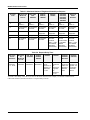
Function Code 01 – Read Digital Output Status
Description
Function code 01 (0X references) is used to read a Digital Output’s (DO) ON/OFF status of the slave device
in a binary data format. All binary data transferred using function code 01 is mapped into bytes.
The specific number of Dos available in an instrument or available via one Function Code 01 message is
instrument-model specific.
Broadcast is not supported.
Query
The query message specifies the starting DO and the quantity of coils to read. Dos are addressed starting at
zero: DO 1 through 16 are addressed as 0 through 15 respectively.
Query message format for function code 01
Slave
Address
Function
Code
Starting
Address
High
Starting
Address
Low
Number
DO
High
Number
DO
Low
CRC
CRC
Example: Read Dos number 1 to 7 from slave at address 02.
02 01 00 00 00 07 CRC CRC
Response
The DO status in the response message is packed as one DO per bit of the data field. Status is indicated as: 1
= ON; 0 = OFF. The LSB of the first data byte contains the DO addressed in the query. The other Dos
follow toward the high order end of this byte, and from low order to high order in subsequent bytes.
If the returned DO quantity is not a multiple of eight, the remaining bits in the final data byte will be padded
with zeros (toward the high order end of the byte). The byte count field specifies the quantity of data bytes
returned.
Response message format for function code 01
Slave
Address
Function
Code
Byte
Count
Data
Data
…
CRC
CRC
Example: Dos number 2 and 7 are on, all others are off.
02 01 01 42 CRC CRC
In the response the status of Dos 1 – 7 is shown as the byte value 42 hex, or 0100 0010 binary. DO 8 is the
MSB of this byte, and DO 1 is the LSB. Left to right, the status of DO 7 through 1 is: ON-OFF-OFF-OFFOFF-ON-OFF. DO #8 was not requested and so bit #7 or the MSB was padded with a 0.
10/04
Modbus® RTU Serial Communications User Manual
13
Modbus RTU Function Codes
Table 3-5 DR4500 Digital Output Mapping
Coil Number
Instrument Function
1
Alarm Relay #1
2
Alarm Relay #1
3
Control Relay #1
4
Control Relay #2
5
Control Relay #3
6
Control Relay #4
Table 3-6 UDC2300/UDC2500/UDC3200/UDC3300 DO Mapping
Coil Number
Instrument Function
1
Control Relay Note 1.
2
Alarm Relay #2
3
Alarm Relay #1
Note 1. The reading of this bit is valid only for
Relay Output Type configurations. Not valid for
current outputs
Table 3-7 Herculine Smart Actuators Digital Output Mapping
14
Coil Number
Instrument Function
1
Alarm Relay #1
2
Alarm Relay #2
3
Alarm Relay #3
4
Alarm Relay #4
Modbus® RTU Serial Communications User Manual
10/04
Modbus RTU Function Codes
3.2
Function Code 02 – Read Digital Input Status
Description
Function code 02 (1X references) is used to read a Digital Input’s (DI) ON/OFF status of the slave device in
a binary data format. All binary data transferred using function code 02 is mapped into bytes.
The specific number of inputs available in an instrument or available via one Function Code 02 message is
instrument-model specific.
Broadcast is not supported.
Query
The query message specifies the starting input and the quantity of inputs to read. Inputs are addressed
starting at zero: input 1 through 16 are addressed as 0 through 15 respectively
Query message format for function code 02
Slave
Address
Function
Code
Starting
Address
High
Starting
Address
Low
Number
Inputs
High
Number
Inputs
Low
CRC
CRC
Example: Read inputs number 1 to 7 from slave at address 02.
02 02 00 00 00 07 CRC CRC
Response
The input status in the response message is packed as one input per bit of the data field. Status is indicated
as: 1 = ON; 0 = OFF. The LSB of the first data byte contains the input addressed in the query. The other
inputs follow toward the high order end of this byte, and from low order to high order in subsequent bytes.
If the returned input quantity is not a multiple of eight, the remaining bits in the final data byte will be
padded with zeros (toward the high order end of the byte). The byte count field specifies the quantity of data
bytes returned.
Response message format for function code 02
Slave
Address
Function
Code
Byte
Count
Data
Data
…
CRC
CRC
Example: Inputs number 2 and 7 are on, all others are off.
02 02 01 42 CRC CRC
In the response the status of inputs 1 – 7 is shown as the byte value 42 hex, or 0100 0010 binary. Input 8 is
the MSB of this byte, and input 1 is the LSB. Left to right, the status of input 7 through 1 is: ON-OFF-OFFOFF-OFF-ON-OFF. Input #8 was not requested and so bit #7 or the MSB was padded with a 0.
10/04
Modbus® RTU Serial Communications User Manual
15
Modbus RTU Function Codes
3.3
Function Codes 03/04 – Read Input Registers
Description
Function code 03 (4X references) or Function code 04 (3X references) is used to read the binary contents of
input registers in the slave referenced in Appendix A. Function codes 3 and 4 are not restricted to inputs.
They may transmit alarm status, control parameters, etc.
The specific supported registers available in an instrument or available via one Function Code 03/04
message is instrument-model specific. When a master station requests a register that is not supported by the
specific device the slave will respond with zeros for that register.
If a request is made to an address that does not exist in the map in Appendix A, the instrument is to honor
that request and return zeros. This behavior will greatly enhance the bandwidth on the link vs. making
several different requests for non-contiguous data elements. (i.e. Consider a device that contains AI #1 and
AI #3 and for some reason AI #2 is an invalid request.) The contiguous method would allow the read of AI
#1 through AI #3 and the data location for AI #2 would be zeros.
Broadcast is not supported.
Query
The query message specifies the starting register and quantity of registers to be read. Registers are addressed
starting at zero: registers 1-16 are addressed as 0-15.
Query message format for function code 03/04
Slave
Address
Function
Code
Starting
Address
High
Starting
Address
Low
Number
Addresses
High
Number
Addresses
Low
CRC
CRC
Example: Read analog inputs #1 and #2 in addresses 1800-1803 as floating point values from a slave at
address 02.
02 04 18 00 00 04 CRC CRC
16
Modbus® RTU Serial Communications User Manual
10/04
Modbus RTU Function Codes
Response
The register data in the response message are packed as two bytes per register. For each register, the first
byte contains the high order bits and the second contains the low order bits.
The floating point values require two consecutive registers. A request for a single floating point value must
be for two registers. The first 16 bits of the response contain the IEEE MSB of the float value. The second
16 bits of the response contain the IEEE LSB of the float value. (See Section 2.3.) If the master station
requests only one register at an address of a floating point value, the slave may respond with an exception
with illegal data address code.
The Modbus RTU protocol has a single byte count for function codes 03 and 04, therefore the Modbus RTU
protocol can only process up to 64 floating point and 127 integer values in a single request.
Response message format for function codes 03/04
Slave
Address
Function
Code
Byte
Count
Data
Data
…
CRC
CRC
Example: Analog inputs #1 and #2 as floating point values where AI #1 = 100.0 and AI #2 = 55.32
02 04 08 42 C8 00 00 47 AE 42 5D CRC CRC
10/04
Modbus® RTU Serial Communications User Manual
17
Modbus RTU Function Codes
3.4
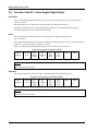
Function Code 05 – Force Single Digital Output
Description
Force a single Digital Output (DO) (0X reference) to either ON or OFF. These are the same Dos used in
Function Code 01.
When broadcast, the same function forces the same DO in all attached slave devices.
Only supported by RSX, VPR, VRX, and UDC5300 instruments. These instruments do not support
broadcast, and forcing can only be done in the Run mode.
Query
The query message specifies the DO to be forced. Registers are addressed starting at zero:
DO 1 is address 0.
The requested ON/OFF state is specified by a constant in the query data field. A value of FF 00 hex requests
it to be ON. A value of 00 00 hex requests it to be OFF.
RSX, VPR, VRX, and UDC5300 products support a value of FF FF to release the force.
Query message format for function code 05
Slave
Address
Function
Code
DO
Address
High
DO
Address
Low
Force
Data
High
Force
Data
Low
CRC
CRC
Example: Force DO 6 ON in a slave at address 02.
02 05 00 06 FF 00 CRC CRC
Response
The normal response is an echo of the query, returned after the DO state has been forced.
Response message format for function code 05
Slave
Address
Function
Code
DO
Address
High
DO
Address
Low
Force
Data
High
Force
Data
Low
CRC
CRC
Example: Force DO 6 ON in a slave at address 02.
02 05 00 06 FF 00 CRC CRC
18
Modbus® RTU Serial Communications User Manual
10/04
Modbus RTU Function Codes
3.5
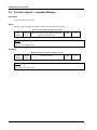
Function Codes 06 – Preset Single Register
Description
Presets an integer value into a single register (4X references). When broadcasted, the function presets the
same register references in all attached slaves.
The specific supported registers available in an instrument via a Function Code 06 message may be
instrument-model specific. However, every instrument that supports the register assignments specified in
Appendix A with an access type “W” and integer and bit packed data types, supports writing to those
specified registers via Function Code 06.
Query
The query message specifies the register references to be preset. Registers are addressed starting at zero:
Register 1 is addressed as 0.
Query message format for function code 06
Slave
Address
Function
Code
Address
High
Address
Low
Preset
Data
High
Preset
Data
Low
CRC
CRC
Example: Set Loop #1 to Auto (address 00Fah) to a slave at address 02.
02 06 00 FA 00 01 CRC CRC
Response
The normal response is an echo of the query returned after the register contents have been preset.
Response message format for function code 06
Slave
Address
Function
Code
Address
High
Address
Low
Preset
Data
High
Preset
Data
Low
CRC
CRC
Example: Set Loop #1 to Auto (address 00Fah) to a slave at address 02.
02 06 00 FA 00 01 CRC CRC
10/04
Modbus® RTU Serial Communications User Manual
19
Modbus RTU Function Codes
3.6
Function Code 08 – Loopback Message
Description
Echoes received query message.
Query
Message can be any length up to half the length of the data buffer minus 8 bytes.
Query message format for function code 08
Slave
Address
Function
Code
Any data, length limited to approximately half
the length of the data buffer
CRC
CRC
CRC
CRC
Example:
02 08 01 02 03 04 CRC CRC
Response
Response message format for function code 08
Slave
Address
Function
Code
Data bytes received
Example:
02 08 01 02 03 04 CRC CRC
20
Modbus® RTU Serial Communications User Manual
10/04
Modbus RTU Function Codes
3.7
Function Codes 16 (10h) – Preset Multiple Registers
Description
Presets values into a sequence of holding registers (4X references). When broadcasted, the function presets
the same register references in all attached slaves.
The specific supported registers available in an instrument via a Function Code 16 (10h) message may be
instrument-model specific. However, every instrument that supports the register assignments specified in
Appendix A with an access type “W”, supports writing to those specified registers via Function Code 16
(10h).
Query
The query message specifies the register references to be preset. Registers are addressed starting at zero:
Register 1 is addressed as 0.
Query message format for function code 16 (10h)
Slave
Address
Function
Code
Starting
Address
High
Start
Address
Low
Number
Addresses
High
Number
Addresses
Low
Byte
Count
Data
CRC
CRC
Example: Preset Variable#1 (address 1880h) to 100.0 from a slave at address 02.
02 10 18 80 00 02 04 42 C8 00 00 CRC CRC
Response
The normal response returns the slave address, function code, starting address and the quantity of registers
preset.
The floating-point values require two consecutive addresses. A request to preset a single floating point value
must be for two addresses. The byte order of the floating-point number is determined by the setting of the
byte swap configuration value. In this example the byte swap order is FP B. Refer to subsection 2.3. The
first 16 bits of the response contain the IEEE MSB of the float value. The second 16 bits of the response
contain the IEEE LSB of the float value. The Byte order is configurable See Subsection 0. If the master
station requests only one address at an address of a floating point value the slave will respond with an illegal
data address exception (See Section 4) code.
Response message format for function code 16 (10h)
Slave
Address
Function
Code
Starting
Address
High
Start
Address
Low
Number
Addresses
High
Number
Addresses
Low
CRC
CRC
Example: Response from preset Constant #1 (address 1880h) to 100.0 from a slave at address 02.
02 10 18 80 00 02 CRC CRC
10/04
Modbus® RTU Serial Communications User Manual
21
Modbus RTU Function Codes
3.8
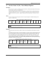
Function Code 17 (11h) – Report Device ID
Description
Function code 17 (11h) is used to report the Device Information that includes information like: Slave ID,
device description, and firmware version.
Query
The query message specifies the function code only.
Query message format for function code 17 (11h)
Slave
Address
Function
Code
CRC
CRC
Example: Read Device ID from a slave at address 02.
02 11 CRC CRC
Response
The response is a record format describing the instrument.
Response message format for function code 17 (11h)
Slave
Address
Function
Code
Byte
Count
Slave
ID
Run
Indicator
Status
Device
Specific
Data
CRC
CRC
Slave ID – The number associated with the device.
(one byte) (byte 3)
Slave ID
(hex)
N/A
18
25
43
45
23
26
32
Device Type
DPR100 (Does not support
11h)
DPR180
DPR250
DR4300
DR4500
UDC2300
UDC2500
UDC3200
Slave ID
(hex)
Device Type
33
UDC3300
35
53
02
63
10
11
20
05
UDC3500
UDC5300, RSX, VPR, VRX
UDC6000
UDC6300
10260S
11280S
SA2001, SA2002
Minitrend V5, Multitrend
Plus V5
Run Indicator Status:
(one byte) (byte 4)
00=OFF; FF=ON
22
Modbus® RTU Serial Communications User Manual
10/04
Modbus RTU Function Codes
+Device Specific Data:
Device
Description
Model
ID
Device
Class
ID
Device
Mapping
Device Description:
16 Character ASCII Message (zero filled) (bytes 5-20).
Device Specific. Usually contains Device Tag + Version Number
Device Type
Device Description
DPR100
N/A
DPR180
DPR180 xxx.yy
DPR250
DPR250 xxx.yy
DR4300
DR4300 x.y
DR4500
DR4500 x.y
RSX
RSX x.y
VPR100/VRX100
Version 5.0 – 7.0 VPR/VRX x.y
Version ≥ 8.0 VRX100 x.y
VRX150
VRX150 x.y
VRX180
VRX180/250 x.y
UDC2300
UDC2300 x.y
UDC2500
UDC2500 x.y
UDC3200
UDC3200 x.y
UDC3300
UDC3300 x.y
UDC3500
UDC3500 x.y
UDC5300
UDC5300 x.y
UDC6000
UDC6000 x.y
UDC6300
UDC6300 x.y
10260S
10260S x.y
11280S
11280S x.y
SA2001, SA2002
SA200n x.y
Minitrend V5
Minitrend nn.v v
Multitrend Plus V5
Multitrend Plus nn.v v
x.y = version of instrument, nn.v v = software version and revision
Model ID:
The Model Identification (Device type specific). (one byte) (byte 21)
Model ID
00
10/04
Description
None
Modbus® RTU Serial Communications User Manual
23
Modbus RTU Function Codes
Device Class ID:
The Device Classification. (one byte) (byte 22)
Class ID
Class
00
Generic Class (Fixed Address Mapable)
01-FF
Future
Generic Class (00) Device Mapping:
Describes the I/O and feature mapping.
Number of
Records
Record
#1
Record
#2
Record
...
Record
#n
Number of records is always 5 for the Minitrend V5 and Multitrend Plus V5.
Number of Records:
1 Byte unsigned value 00-FFh (byte 23)
Record Description:
Byte
Description
00
Type of Data Element
(See Data Element Values Table Below)
01
Starting Address of Data Element Record (High)
02
Starting Address of Data Element Record (Low)
03
Number of Data Elements (High)
04
Number of Data Elements (Low)
Data Element Values Table:
Value
Description
00*
Analog Inputs
01
Analog Outputs
02*
Discrete Inputs
03*
Discrete Outputs
04
Control Loops
05
Set Point Programmers
06*
Math, Calculated Values, or Variables
07
Constants
08
Alarms
09*
Totalizers
* These data elements are the 5 data records sent from the Minitrend and the
Multitrend Plus V5 recorders.
24
Modbus® RTU Serial Communications User Manual
10/04
Modbus RTU Exception Codes
4. Modbus RTU Exception Codes
Introduction
When a master device sends a query to a slave device it expects a normal response. One of four possible
events can occur from the master’s query:
•
Slave device receives the query without a communication error and can handle the query normally.
It returns a normal response.
•
Slave does not receive the query due to a communication error.
No response is returned. The master program will eventually process a time-out condition for the
query.
•
Slave receives the query but detects a communication error (parity, LRC or CRC).
No response is returned. The master program will eventually process a time-out condition for the
query.
•
Slave receives the query without a communication error but cannot handle it (i.e., request is to a nonexistent coil or register).
The slave will return with an exception response informing the master of the nature of the error (Illegal
Data Address.)
The exception response message has two fields that differentiate it from a normal response:
Function Code Field:
In a normal response, the slave echoes the function code of the original query in the function code
field of the response. All function codes have a most-significant bit (MSB) of 0 (their values are below
80 hex). In an exception response, the slave sets the MSB of the function code to 1. This makes the
function code value in an exception response exactly 80 hex higher than the value would be for a
normal response.
With the function code’s MSB set, the master’s application program can recognize the exception
response and can examine the data field for the exception code.
Data Field:
In a normal response, the slave may return data or statistics in the data field. In an exception response,
the slave returns an exception code in the data field. This defines the slave condition that caused the
exception.
Query
Example: Internal slave error reading 2 registers starting at address 1820h from slave at slave address 02.
02 03 18 20 00 02 CRC CRC
Response
Example: Return MSB in Function Code byte set with Slave Device Failure (04) in the data field.
83 04 CRC CRC
10/04
Modbus® RTU Serial Communications User Manual
25
Modbus RTU Exception Codes
Table 4-1 Modbus RTU Data Layer Status Exception Codes
Exception
Code
26
Definition
Description
01
Illegal Function
The message received is not an allowable action for
the addressed device.
02
Illegal Data Address
The address referenced in the function-dependent data
section of the message is not valid in the addressed
device.
03
Illegal Data Value
The value referenced at the addressed device location
is no within range.
04
Slave Device Failure
The addressed device has not been able to process a
valid message due to a bad device state.
06
Slave Device Busy
The addressed device has ejected a message due to a
busy state. Retry later.
07
NAK,
Negative Acknowledge
The addressed device cannot process the current
message. Issue a PROGRAM POLL to obtain devicedependent error data.
09
Buffer Overflow
The data to be returned for the requested number of
registers is greater than the available buffer space.
Function Code 20 only.
Modbus® RTU Serial Communications User Manual
10/04
Appendix A: Register Map
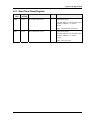
A. Appendix: Register Map
What’s in this appendix?
This appendix describes all paramters accessible by Function Code 03, 04, 06 and 10h. Section A.1 gives
a global overview of each function and its addresses/registers. Sections A.2 through A.20 contain the
details on each function and each of its parameters.
Your particular instrument may not contain all parameters shown. If you see a function that is not on your
instrument, either it is not available for that instrument model or it is an option you did not purchase. If a
function is not available for your instrument, that will be indicated.
A.1
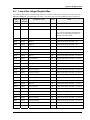
Register Map Overview
Table A-1describes the global register map for Function Code 03, 04, 06 and 10h. Details on each address
are in sections A.2 through A.20. Your particular instrument may not contain all functions or parameters
shown. For example, some instruments contain only one or two loops, do not contain calculated values,
setpoint programmers, etc.
Conversion of address (hex) number to register (decimal) number.
To convert the address number to the register number, convert the address from hexidecimal to decimal
and add 40001. Registers are addressed starting at zero: registers 1 – 16 are addressed as 0 – 15.
To convert the register number to the address number, subtract 40001 from the register and convert to hex.
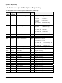
Table A-1 Global Register Map
Start Address
(hex)
0000
0040
0100
0140
0240
0340
0440
0540
0640
0740
0800
0840
0940
0A40
0B40
0C40
0D40
0E40
0F40
1040
10/04
End Address
(hex)
< 0040
00FF
013F
01FF
02FF
03FF
04FF
05FF
06FF
07FF
081C
08FF
09FF
0AFF
0BFF
0CFF
0DFF
0EFF
0FFF
10FF
Description
Miscellaneous Parameters or Loop #1 Integer
Loop #1 (floating point & bit packed)
Loop #2 Integer
Loop #2 (floating point & bit packed)
Loop #3 (floating point & bit packed)
Loop #4 (floating point & bit packed)
Loop #5 (floating point & bit packed)
Loop #6 (floating point & bit packed)
Loop #7 (floating point & bit packed)
Loop #8 (floating point & bit packed)
DR4300, DR4500 Chart
Loop #9 (floating point & bit packed)
Loop #10 (floating point & bit packed)
Loop #11 (floating point & bit packed)
Loop #12 (floating point & bit packed)
Loop #13 (floating point & bit packed)
Loop #14 (floating point & bit packed)
Loop #15 (floating point & bit packed)
Loop #16 (floating point & bit packed)
Loop #17 (floating point & bit packed)
Modbus® RTU Serial Communications User Manual
See
Subsection
A.2 or A.3
A.4
A.2.2
A.4
27
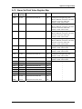
Appendix A: Register Map
Start Address
(hex)
28
End Address
(hex)
1140
1240
1340
1440
1540
1640
1740
1800
1880
18C0
1AC0
1AD0
1B00
1B80
1B90
1B99
1BE0
1BF0
1C00
1E00
1E10
1E20
1E30
1E40
1F00
1F40
1F80
1FC0
27D0
11FF
12FF
13FF
14FF
15FF
16FF
17FF
187F
18BF
1ABF
1ACF
1AFF
1B7F
1B83
1B91
1BAB
1BE6
1BFF
1DFF
1E0F
1E1F
1E2F
1E3F
1E67
1F3F
1F7F
1FBF
1FFF
2806
2800
2A00
2C00
2E00
29FF
2BFF
2DFF
2FFF
Description
Loop #18 (floating point & bit packed)
Loop #19 (floating point & bit packed)
Loop #20 (floating point & bit packed)
Loop #21 (floating point & bit packed)
Loop #22 (floating point & bit packed)
Loop #23 (floating point & bit packed)
Loop #24 (floating point & bit packed)
Analog Input Value (#1-#64)
Communication or Constant Value (#1 - #32)
Math or Calculated Value (#1 - #256)
Math or Calculated Value Status (#1 - #256)
Herculine Smart Actuator Values Register Map
Totalizer Value (#1 - #64)
Totalizer Status (Bit Packed) (#1 - #64)
Shed Timer Reset
Maintenance (HealthWatch) Values
Time
Alarm Status (Bit Packed) (#1 - #256)
Alarm Set Point Value (#1 - #256)
Set Point Programmer #1
Set Point Programmer #2
Set Point Programmer #3
Set Point Programmer #4
Smart Actuator Maintenance Data
Set Point Programmer #1 Additional Values
Set Point Programmer #2 Additional Values
Set Point Programmer #3 Additional Values
Set Point Programmer #4 Additional Values
Herculine Smart Actuator Factory Data Register
Map
Set Point Programmer #1 Segments
Set Point Programmer #2 Segments
Set Point Programmer #3 Segments
Set Point Programmer #4 Segments
Modbus® RTU Serial Communications User Manual
See
Subsection
A.5
A.6
A.7
0
A.19
A.9
A.10
A.11
A.12
0
A.14
A.15
A.16
A.21
A.17
A.20
A.18
10/04
Appendix A: Register Map
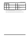
A.2
Miscellaneous Register Map
A.2.1 RSX, VPR, VRX, UDC5300 Miscellaneous Register Map
Address
(hex)
Register
(decimal)
0000
40001
Parameter Name
Instrument Mode
Access
R/W
Notes
Bit Packed
Indicators:
Bit 0: 1:Diagnostic
Bit 1: 1:Calibration
Bit 2: 1:Maintenance/Offline mode
Bit 3: 1:Program mode
Bit 4: 1:Reset Unit/Force Cold Start
(Write Only)
Bit 5: 1:On-Line/Run mode
Bit 6…15: Unused
0001
40002
Configuration Select
W
Signed 16 bit integer
0: Clear Configuration
(Preserves Calibration)
0002
40003
Load Recipe or
Program Number
10/04
R/W
Floating Point
VRX/VPR
Read: Active program number
Write: Load program (write is allowed
only when SPP is in Ready or At End)
Modbus® RTU Serial Communications User Manual
29
Appendix A: Register Map
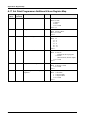
A.2.2 DR4300, DR4500 Chart Record Map
Address
(hex)
Register
(decimal)
Parameter Name
Access
Notes
0800
42049
Chart Speed (Hours/rev)
R
Floating Point in Engineering Units.
Note 1
0802
42051
# Chart Divisions
R
Floating Point in Engineering Units.
0804
42053
Chart Status
R
Floating Point
0.0 = hold; 1.0 = running.
0806
42055
Pen 1
R
Floating Point
0.0 = disabled; 1.0 = enabled
0808
42057
Pen 1 High Value
R
Floating Point in Engineering Units.
Note 1
080A
42059
Pen 1 Low Value
R
Floating Point in Engineering Units.
Note 1
080C
42061
Pen 2
R
Floating Point
0.0 = disabled; 1.0 = enabled
080E
42063
Pen 2 High Value
R
Floating Point in Engineering Units.
0810
42065
Pen 2 Low Value
R
Floating Point in Engineering Units.
0812
42067
Pen 3
R
Floating Point
0.0 = disabled; 1.0 = enabled
0814
42069
Pen 3 High Value
R
Floating Point in Engineering Units.
0816
42071
Pen 3 Low Value
R
Floating Point in Engineering Units.
0818
42073
Pen 4
R
Floating Point
0.0 = disabled; 1.0 = enabled
081A
42075
Pen 4 High Value
R
Floating Point in Engineering Units.
081C
42077
Pen 4 Low Value
R
Floating Point in Engineering Units.
NOTE 1: The DR4300 only supports the noted registers. All registers are supported by the DR4500.
30
Modbus® RTU Serial Communications User Manual
10/04
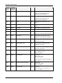
Appendix A: Register Map
A.3
Loop Value Integer Register Map
The following table applies to the following instruments: UDC2300, UDC2500, UDC3200, UDC3300, UDC3500,
DR4300 and DR4500. This table applies to Loops 1-24 except Loops 2-24 use the addresses shown in Table A-1
Address
(hex)
Register
(decimal)
Parameter Name
Access
Notes
0000
40001
PV
R
Signed 16 bit integer Prescale * 10 Note 5
0001
40002
RV; Remote Set Point; SP2
R
Signed 16 bit integer Prescale * 10
0002
40003
Working Set Point
R/W
Signed 16 bit integer Prescale * 10 Note 5
On a write the instrument will update the
proper set point according to the loop’s
currently selected set point.
0003
40004
Output
R/W
Signed 16 bit integer Prescale * 10
0004
40005
Input #1
R
Signed 16 bit integer Prescale * 10
0005
40006
Input #2
R
Signed 16 bit integer Prescale * 10
0006
40007
Gain #1 (Prop Band #1 if active)
R/W
Signed 16 bit integer Prescale * 10
0007
40008
Direction
R
Signed 16 bit integer Prescale * 10
0008
40009
Reset #1
R/W
Signed 16 bit integer Prescale * 10 Note 1
0009
40010
Rate #1
R/W
Signed 16 bit integer Prescale * 10 Note 1
000A
40011
Cycle Time #1
R/W
Signed 16 bit integer Prescale * 10 Note 2
000B
40012
PV Low Range
R
Signed 16 bit integer Prescale * 10
000C
40013
PV High Range
R
Signed 16 bit integer Prescale * 10
000D
40014
Alarm #1 SP #1
R/W
Signed 16 bit integer Prescale * 10 Note 7
000E
40015
Alarm #1 SP #2
R/W
Signed 16 bit integer Prescale * 10 Note 7
000F
40016
Alarm #1 Action
R
Signed 16 bit integer Prescale * 10 Note 6
0010
40017
Gain #2 (Prop Band #2 if active)
R/W
Signed 16 bit integer Prescale * 10
0011
40018
Deadband
R/W
Signed 16 bit integer Prescale * 10
0012
40019
Reset #2
R/W
Signed 16 bit integer Prescale * 10 Note 1
0013
40020
Rate #2
R/W
Signed 16 bit integer Prescale * 10 Note 1
0014
40021
Cycle Time #2
R/W
Signed 16 bit integer Prescale * 10 Note 2
0015
40022
SP1; LSP #1
R/W
Signed 16 bit integer Prescale * 10 Note 5
0016
40023
LSP #2
R/W
Signed 16 bit integer Prescale * 10 Note 5
0017
40024
Alarm #2 SP #1
R/W
Signed 16 bit integer Prescale * 10 Note 7
0018
40025
Alarm #2 SP #2
R/W
Signed 16 bit integer Prescale * 10 Note 7
0019
40026
Alarm #2 Action
R
Signed 16 bit integer Prescale * 10 Note 6
001A
40027
SP Low Limit
R/W
Signed 16 bit integer Prescale * 10 Note 5
001B
40028
SP High Limit
R/W
Signed 16 bit integer Prescale * 10 Note 5
10/04
Modbus® RTU Serial Communications User Manual
31
Appendix A: Register Map
Address
(hex)
Register
(decimal)
001C
40029
Parameter Name
Working Set Point
Access
R/W
Notes
Signed 16 bit integer Prescale * 10 Note 5
On a write to this register the instrument
will update the proper set point according to
the loop’s currently selected set point.
Use this register for operator set point value
changes ONLY. Use SP Override for
computer-generated set point values.
001D
40030
Output Low Limit
R/W
Signed 16 bit integer Prescale * 10
001E
40031
Output High Limit
R/W
Signed 16 bit integer Prescale * 10
001F
40032
Output Working Value
R/W
Signed 16 bit integer Prescale * 10
0020
40033
PV Override Value
R/W
Signed 16 bit integer Prescale * 10
0021
40034
SP Override Value
R/W
Signed 16 bit integer Prescale * 10 Note 5
0022
40035
Output Override Value
R/W
Signed 16 bit integer Prescale * 10
0023
40036
Ratio
R/W
Signed 16 bit integer Prescale * 10 Note 4
0024
40037
Bias
R/W
Signed 16 bit integer Prescale * 10 Note 4
0025
40038
Deviation
R
Signed 16 bit integer Prescale * 10
0026
40039
LSP #3
R/W
Signed 16 bit integer Prescale * 10 Note 5
0027
40040
Percent Carbon Monoxide - CO
R/W
Signed 16 bit integer Prescale*1000 Note 3
0028
40041
Decimal Point
R/W
Signed 16 bit integer Prescale* 1
0029
40042
Alg1 Bias
R/W
Signed 16 bit integer Prescale * 10 Note 8
002A
40043
Alg2 Bias
R/W
Signed 16 bit integer Prescale * 10 Note 9
003A
40059
Auto/Manual State
R/W
Bit Packed
Bit 0: 0:Manual; 1:Auto
Bit 1-15: Unused
003B
003C
003D
32
40060
40061
40062
Set Point State
Remote/Local Set Point State
Tune Set State
R/W
R/W
R/W
Note 3
Note 3
Bit Packed
Bit 0: 0:SP1; 1:SP2
Bit 1-15: Unused
UDC3300: Bit 1: 1:SP3
Note 3
Bit Packed
Bit 0: 0:LSP; 1:RSP
Bit 1-15: Unused
Note 3
Bit Packed
Bit 0: 0:Tune Set #1; 1:Tune Set #2
Bit 1-15: Unused
Note 3
Modbus® RTU Serial Communications User Manual
10/04
Appendix A: Register Map
Address
(hex)
Register
(decimal)
003E
40063
Parameter Name
Loop Status
Access
R
Notes
Bit Packed
Bit 0: Mode: 0:Manual; 1:Auto
Bit 1: Set Point: 0:SP1; 1:SP2
Bit 2: Remote/Local: 0:LSP; 1:RSP
Bit 3: Tune Set: 0:Set #1; 1:Set #2
Bit 4-15: Reserved
Note 3
Note 1 :UDC3200, UDC3300, UDC3500 uses a prescale of 100 for this parameter.
Note 2: UDC3200, UDC3300, UDC3500 uses a prescale of 1 for this parameter.
Note 3: UDC3200, UDC3300, UDC3500 only.
Note 4: UDC3200, UDC3300, UDC3500 Ratio and Bias are CSP parameters.
Note 5: In the UDC3200, UDC3300, or UDC3500, if the input type is configured as Carbon and the input algorithm
is configured for one of the carbon selections, the prescale value is derived from the configured decimal
point.
Note 6: Not supported by UDC2300, UDC2500, UDC3200, UDC3300, or UDC3500
Note 7: Loop 1 Address only.
Note 8: In the UDC3200, UDC3300, or UDC3500, if the Algorithm 1 type is configured for weighted average, RH,
Summer, Sq. Root Mult-Div, Sq Root Mult, Mult-Div, Mult, Carbon A-D, FCC, Dew Point, or Oxygen, the
prescale value is derived from the configured decimal point.
Note 9: In the UDC3300, or UDC3500 if the Algorithm 2 type is configured for weighted average, A-B/C, Sq Root
Mult-Div, Sq Root Mult, Mult-Div, Mult, or Dew Point, the prescale value is derived from the configured
decimal point.
10/04
Modbus® RTU Serial Communications User Manual
33
Appendix A: Register Map
A.4
Loop Value Register Map
This table contains addresses of Loop #1; see Table A-1 on page 27 for addresses of other loops.
Address
(hex)
Register
(decimal)
Parameter Name
Access
Notes
0040
40065
PV
R
Floating Point in Engineering Units.
0042
40067
RV; Remote Set Point; SP2
R
Floating Point in Engineering Units.
RSX, VPR, VRX, UDC5300 allow writing
this value when SP2 is local (not
connected)
0044
40069
Working Set Point
R
Floating Point in Engineering Units.
RSX, VRX, VPR, UDC5300,: R/W
On a write to this register the instrument
will update the proper set point according
to the loop’s currently selected set point.
0046
40071
Output
R/W
Floating Point in Engineering Units.
UDC2500, UDC3200, UDC3500
Read Only
0048
40073
Input #1
R
Floating Point in Engineering Units.
004C
40077
Gain #1 (Prop Band #1 if active)
R/W
Floating Point
UDC3300 or UDC3500: For loop #2, this cell
is Gain #3
004E
40079
Direction
R
Floating Point
0.0=Direct; 1.0=Reverse
0050
40081
Reset #1
R/W
Floating Point in Repeats/Minute or
Minutes/Repeat.
UDC3300 or UDC3500: For loop #2, this cell
is Reset #3
0052
40083
Rate #1
R/W
Floating Point in Minutes
UDC3300 or UDC3500: For loop #2, this cell
is rate #3
0054
40085
Cycle Time #1
R/W
Floating Point in Seconds.
Read-only for UDC2300, UDC3300.
UDC3300, UDC3500: For loop #2, this cell is
Cycle Time #3
0056
40087
PV Low Range
R
Floating Point in Engineering Units.
0058
40089
PV High Range
R
Floating Point in Engineering Units.
005A
40091
Alarm #1 SP #1
R/W
Floating Point in Engineering Units.
Note 2
005C
40093
Alarm #1 SP #2
R/W
Floating Point in Engineering Units.
Note 2
005E
40095
unused
34
Modbus® RTU Serial Communications User Manual
10/04
Appendix A: Register Map
Address
(hex)
Register
(decimal)
0060
40097
Parameter Name
Gain #2 (Prop Band #2 if active)
Access
R/W
Notes
Floating Point
UDC3300 or UDC3500: For loop #2, this cell
is Gain #4
0062
40099
Deadband
R/W
Floating Point
0064
40101
Reset #2
R/W
Floating Point in Repeats/Minute or
Minutes/Repeat.
UDC3300 or UDC3500: For loop #2, this cell
is Reset #4
0066
40103
Rate #2
R/W
Floating Point in Minutes
UDC3300 or UDC3500: For loop #2, this cell
is rate #4
0068
40105
Cycle Time #2
R/W
Floating Point in Seconds.
Read-only UDC2300, UDC3300.
UDC3300, UDC3500: For loop #2, this cell is
Cycle Time #4
006A
40107
SP1; LSP #1
R/W
Floating Point in Engineering Units.
006C
40109
LSP #2
R/W
Floating Point in Engineering Units.
006E
40111
Alarm #2 SP #1
R/W
Floating Point in Engineering Units.
Note 2
0070
40113
Alarm #2 SP #2
R/W
Floating Point in Engineering Units.
Note 2
0072
40115
unused
0074
40117
SP Low Limit
R/W
Floating Point in Engineering Units.
0076
40119
SP High Limit
R/W
Floating Point in Engineering Units.
0078
40121
Working Set Point
R/W
Floating Point in Engineering Units.
On a write to this register the instrument
will update the proper set point according
to the loop’s currently selected set point.
NOTE: Use this register for operator set
point value changes ONLY. Use SP
Override for computer-generated set
point values.
DR4300, DR4500: READ ONLY
007A
40123
Output Low Limit
R/W
Floating Point in Engineering Units.
007C
40125
Output High Limit
R/W
Floating Point in Engineering Units.
007E
40127
Output Working Value
R/W
Floating Point in Engineering Units.
0080
40129
PV Override Value
R/W
Floating Point in Engineering Units.
UDC2300, UDC2500, UDC3200,
UDC3300, UDC3500 ONLY
10/04
Modbus® RTU Serial Communications User Manual
35
Appendix A: Register Map
Address
(hex)
Register
(decimal)
0082
40131
Parameter Name
SP Override Value
Access
R/W
Notes
Floating Point in Engineering Units.
UDC2300, UDC2500, UDC3200,
UDC3300, UDC3500 ONLY
0084
40133
Output Override Value
R/W
Floating Point in Engineering Units.
UDC2300, UDC2500, UDC3200,
UDC3300, UDC3500 ONLY
0086
40135
Ratio
R/W
Floating Point in Engineering Units.
Note 1.
0088
40137
Bias
R/W
Floating Point in Engineering Units.
Note 1.
008A
40139
Deviation
R
Floating Point in Engineering Units.
008C
40141
LSP #3
R/W
Floating Point in Engineering Units.
009E
40159
ALG1 Bias
R/W
Floating Point in Engineering Units
UDC3200, UDC3300, UDC3500 ONLY
00A0
40161
ALG2 Bias
R/W
Floating Point in Engineering Units
UDC3200, UDC3300, UDC3500 ONLY
00A2
40163
Aux Output
R
Floating Point in Engineering Units
UDC2500, UDC3200
00A4
40165
Setpoint Ramp Time
R/W
Floating Point in Engineering Units
UDC2500, UDC3200
00A6
40167
Setpoint Ramp Setpoint
R/W
Floating Point in Engineering Units
UDC2500, UDC3200
00FA
40251
Auto/Manual State
R/W
Bit Packed
Bit 0: 0:Manual; 1:Auto
Bit 1-15: Unused
00FB
40252
Set Point State
R/W
Bit Packed
Bit 0: 0:SP1; 1:SP2
Bit 1-15: Unused
UDC3200, UDC3300, UDC3500 ONLY:
Bit 1: 1:SP3
00FC
40253
Remote/Local Set Point State
R/W
Bit Packed
Bit 0: 0:LSP; 1:RSP
Bit 1-15: Unused
00FD
40254
Tune Set State
R/W
Bit Packed
Bit 0: 0:Tune Set #1; 1:Tune Set #2
Bit 1-15: Unused
36
Modbus® RTU Serial Communications User Manual
10/04
Appendix A: Register Map
Address
(hex)
Register
(decimal)
00FE
40255
Parameter Name
Loop Status
Access
R
Notes
Bit Packed
Bit 0: Mode: 0:Manual; 1:Auto
Bit 1: Set Point: 0:SP1; 1:SP2
Bit 2: Remote/Local: 0:LSP; 1:RSP
Bit 3: Tune Set: 0:Set #1; 1:Set #2
Bit 4: N/A
Bit 5: N/A
Bit 6-15: Reserved
Note 1: UDC2300/UDC2500/UDC3200/UDC3300/UDC3500 Ratio and Bias are CSP parameters.
Note 2: Loop 1 Addresses only.
A.5
Analog Input Value Register Map
Address
(hex)
1800
1802
1804
1806
1808
180A
180C
180E
1810
1812
1814
1816
:
187E
10/04
Register
(decimal)
46145
46147
46149
46151
46153
46155
46157
46159
46161
46163
46165
46167
:
46271
Channel Number
Analog Input #1
Analog Input #2
Analog Input #3
Analog Input #4
Analog Input #5
Analog Input #6
Analog Input #7
Analog Input #8
Analog Input #9
Analog Input #10
Analog Input #11
Analog Input #12
:
Analog Input #64
Access
R
R
R
R
R
R
R
R
R
R
R
R
Notes
Floating Point in Engineering Units.
Number of Inputs vary according to
model numbers
R
Modbus® RTU Serial Communications User Manual
37
Appendix A: Register Map
A.6
Communication or Constant Value Register Map
Address
(hex)
Register
(decimal)
1880
46273
Communication Value #1
R/W
Floating Point in Engineering Units.
DR4500: Input 1 Bias
1882
46275
Communication Value #2
R/W
Floating Point in Engineering Units.
DR4500: Input 2 Bias
1884
46277
Communication Value #3
R/W
Floating Point in Engineering Units.
DR4500: Input 3 Bias
1886
46279
Communication Value #4
R/W
Floating Point in Engineering Units.
DR4500: Input 4 Bias
1888
46281
Communication Value #5
R/W
Floating Point in Engineering Units.
188A
46283
Communication Value #6
R/W
:
188C
46285
Communication Value #7
R/W
:
188E
46287
Communication Value #8
R/W
:
1890
46289
Communication Value #9
R/W
:
1892
46291
Communication Value #10
R/W
:
1894
46293
Communication Value #11
R/W
:
1896
46295
Communication Value #12
R/W
:
1898
46297
Communication Value #13
R/W
:
189A
46299
Communication Value #14
R/W
:
189C
46301
Communication Value #15
R/W
:
189D
46303
Communication Value #16
R/W
:
:
:
18BE
46335
38
Channel Number
Access
Notes
:
Communication Value #32
:
R/W
Modbus® RTU Serial Communications User Manual
:
10/04
Appendix A: Register Map
A.7
Math, Calculated Value, or Variable Register Map
Address
(hex)
Register
(decimal)
18C0
46337
Math Value #1
R
Floating Point in Engineering Units.
Smart Actuator: Position
18C2
46339
Math Value #2
R
Floating Point in Engineering Units.
Smart Actuator: NCS Calibration Voltage
18C4
46341
Math Value #3
R
Floating Point in Engineering Units.
18C6
46343
Math Value #4
R
:
18C8
46345
Math Value #5
R
:
18CA
46347
Math Value #6
R
:
18CC
46349
Math Value #7
R
:
18CE
46351
Math Value #8
R
:
18D0
46353
Math Value #9
R
:
18D2
46355
Math Value #10
R
:
18D4
46357
Math Value #11
R
:
18D6
46359
Math Value #12
R
:
18D8
46361
Math Value #13
R
:
18DA
46363
Math Value #14
R
:
18DC
46365
Math Value #15
R
:
18DE
46367
Math Value #16
R
:
18E0
46369
Math Value #17
R
:
18E2
46371
Math Value #18
R
:
18E4
46373
Math Value #19
R
:
18E6
46375
Math Value #20
R
:
18E8
46377
Math Value #21
R
:
18EA
46379
Math Value #22
R
:
18EC
46381
Math Value #23
R
:
18EE
46383
Math Value #24
R
:
18F0
46385
Math Value #25
R
:
18F2
46387
Math Value #26
R
:
18F4
46389
Math Value #27
R
:
18F6
46391
Math Value #28
R
:
18F8
46393
Math Value #29
R
:
18FA
46395
Math Value #30
R
:
18FC
46397
Math Value #31
R
:
18FE
:
1ABE
46399
:
46847
Math Value #32
R
:
Math Value #256
R
:
:
:
10/04
Channel Number
Access
Notes
Modbus® RTU Serial Communications User Manual
39
Appendix A: Register Map
A.8
Math or Calculated Value Status Register Map
Address
(hex)
Register
(decimal)
1AC0
46849
Channel Number
Math Status #1-#16
Access
R
Notes
Bit Packed:
Bit 0: Math #1 Status
:
Bit 15: Math #16 Status
0: Math OFF
1: Math ON
1AC1
46850
Math Status #17-#32
R
Bit Packed
Bit 0: Math #17 Status
:
Bit 15: Math #32 Status
0: Math OFF
1: Math ON
:
:
1ACF
46864
40
:
Math Status #240 - #256
:
R
Modbus® RTU Serial Communications User Manual
:
:
10/04
Appendix A: Register Map
A.9
Totalizer Value Register Map
Address
(hex)
Register
(decimal)
1B00
46913
Totalizer Value #1
R
1B02
46915
Totalizer Value #2
R
:
1B04
46917
Totalizer Value #3
R
:
1B06
46919
Totalizer Value #4
R
:
1B08
46921
Totalizer Value #5
R
:
1B0A
46923
Totalizer Value #6
R
:
:
:
1B7E
47039
Channel Number
Access
Notes
Floating Point in Engineering Units.
:
Totalizer Value #64
:
R
:
ATTENTION
To reset totalizer to a specific value, write that value to these registers (i.e., to reset totalizer #1 to zero write 0.0 to
register 46913).
10/04
Modbus® RTU Serial Communications User Manual
41
Appendix A: Register Map
A.10 Totalizer Status Register Map
Address
(hex)
Register
(decimal)
1B80
47041
Channel Number
Totalizer Status #1 - #16
Access
R
Notes
Bit Packed
Bit 0: Totalizer #1 Status
Bit 1: Totalizer #2 Status
:
Bit 15: Totalizer #16 Status
0: Totalizer OFF
1: Totalizer ON
1B81
47042
Totalizer Status #17 - #32
R
Bit Packed
Bit 0: Totalizer #17 Status
Bit 1: Totalizer #18 Status
:
Bit 15: Totalizer #32 Status
0: Totalizer OFF
1: Totalizer ON
1B82
47043
Totalizer Status #33 - #48
R
:
1B83
47044
Totalizer Status #49 - #64
R
:
42
Modbus® RTU Serial Communications User Manual
10/04
Appendix A: Register Map
A.11 Shed Timer Reset Register
Address
(hex)
Register
(decimal)
1B90
47057
Channel Number
Reset Shed Timer Loop 1
Access
W
Notes
Signed 16 bit integer
Write this address to clear an infinite shed
condition. (Shedtime = 0) Data is
ignored.
NOTE: UDC3300/UDC2300 ONLY
1B91
47058
Reset Shed Timer Loop 2
W
Signed 16 bit integer
Write this address to clear an infinite shed
condition. (Shedtime = 0) Data is
ignored.
NOTE: UDC3300 ONLY
10/04
Modbus® RTU Serial Communications User Manual
43
Appendix A: Register Map
A.12 Maintenance (HealthWatch) Value Register Map
This table applies to the UDC3300 Expanded and UDC3500 models only.
Address
(hex)
Register
(decimal)
1B99
47064
Maintenance Reset Type
W
Unsigned 16-bit Integer
0: None
6: Counter 2
1: Timer 1
7: Counter 3
2: Timer 2
8: All Counters
3: Timer 3
9: All Timers &
Counters
4: All Timers 10: Ambient Temp
5: Counter 1
1B9A
47065
Timer 1 Configuration
R/W
Unsigned 16-bit Integer
0: Disable
6: Manual Loop 1
1: Last Reset
7: Guaranteed soak
2: Alarm 1 SP1 8: Sooting
3: Alarm 1 SP2 9: DI1 Closed
4: Alarm 2 SP1 10:DI2 Closed
5: Alarm 2 SP2 11: Manual Loop 2
1B9B
47066
Timer 2 Configuration
R/W
Same as Timer 1 Configuration
1B9C
47067
Timer 3 Configuration
R/W
Same as Timer 1 Configuration
1B9D
47068
Counter 1 Configuration
R/W
Unsigned 16-bit Integer
0: Disable
6: DI1
1: Manual Loop 1 7: DI2
2: Alarm 1 SP1 8: Output1 Relay x 1K
3: Alarm 1 SP2 9: Output2 Relay x 1K
4: Alarm 2 SP1 10:Guaranteed soak
5: Alarm 2 SP2 11: Power cycle
1B9E
47069
Counter 2 Configuration
R/W
Same as Counter 1 Configuration
1B9F
47070
Counter 3 Configuration
R/W
Same as Counter 1 Configuration
1BA0
47071
Timer 1 Days
R
Signed 16 bit integer
1BA1
47072
Timer 1 Hours
R
Signed 16 bit integer
1BA2
47073
Timer 1 Minutes
R
Signed 16 bit integer
1BA3
47074
Timer 2 Days
R
Signed 16 bit integer
1BA4
47075
Timer 2 Hours
R
Signed 16 bit integer
1BA5
47076
Timer 2 Minutes
R
Signed 16 bit integer
1BA6
47077
Timer 3 Days
R
Signed 16 bit integer
1BA7
47078
Timer 3 Hours
R
Signed 16 bit integer
1BA8
47079
Timer 3 Minutes
R
Signed 16 bit integer
1BA9
47080
Counter 1
R
Signed 16 bit integer
1BAA
47081
Counter 2
R
Signed 16 bit integer
1BAB
47082
Counter 3
R
Signed 16 bit integer
44
Channel Number
Access
Notes
Modbus® RTU Serial Communications User Manual
10/04
Appendix A: Register Map
A.13 Time Register Map
Address
(hex)
Register
(decimal)
Channel Number
Access
Notes
1BE0
47137
Hours
R/W
0 to 23
1BE1
47138
Minutes
R/W
0 to 60
1BE2
47139
Seconds
R/W
0 to 60
1BE3
47140
Month
R/W
1 to 12
1BE4
47141
Day
R/W
1 to 31
1BE5
47142
Year
R/W
00 to 99
VPR, VRX: accepts the values 0 – 37, 70
– 99, and 1970 – 2037. The values read
are always in the range of 1970 to 2037.
0 – 37 represents 2000 – 2037, 70 – 99
represents 1970 – 1999
DR4500: accepts 0-99 or 1970 – 2037
and ignores the century.
1BE6
47143
Week Day
R/W
0 to 6 (0 = Sunday)
DR4500: R/W
VPR/VRX: ignored
ATTENTION
Clock registers must be written in a single transaction. They can be written in one transaction of registers 47137
through 47142 or one transaction of registers 47137 through 47143.
10/04
Modbus® RTU Serial Communications User Manual
45
Appendix A: Register Map
A.14 Alarm Status Register Map
Address
(hex)
Register
(decimal)
1BF0
47153
Alarm Status #1 - #16
R
1BF1
47154
Alarm Status #17 - #32
R
1BF2
47155
Alarm Status #33 - #48
R
1BF3
1BF4
1BF5
:
1BFF
47156
47157
47158
:
47168
Alarm Status #49 - #64
Alarm Status #65 - #80
Alarm Status #81 - #96
:
Alarm Status #240 - #256
R
R
R
46
Channel Number
Access
:
R
Notes
Bit Packed
Bit 0: Alarm #1 Status
Bit 1: Alarm #2 Status
:
Bit 15: Alarm #16 Status
0: Alarm OFF
1: Alarm ON
Bit Packed
Bit 0: Alarm #17 Status
Bit 1: Alarm #18 Status
:
Bit 15: Alarm #32 Status
0: Alarm OFF
1: Alarm ON
Bit Packed
Bit 0: Alarm #33 Status
Bit 1: Alarm #34 Status
:
Bit 15: Alarm #48 Status
0: Alarm OFF
1: Alarm ON
:
:
:
:
:
Modbus® RTU Serial Communications User Manual
10/04
Appendix A: Register Map
A.15 Alarm Set Point Value Register Map
Address
(hex)
Register
(decimal)
1C00
47169
Alarm Set Point Value #1
R/W
1C02
47171
Alarm Set Point Value #2
R/W
1C04
47173
Alarm Set Point Value #3
R/W
1C06
47175
Alarm Set Point Value #4
R/W
1C08
47177
Alarm Set Point Value #5
R/W
1C0A
47179
Alarm Set Point Value #6
R/W
1C0C
47181
Alarm Set Point Value #7
R/W
1C0E
47183
Alarm Set Point Value #8
R/W
1C10
1C12
1C14
1C16
1C18
1C1A
1C1C
1C1E
:
1DFE
47185
47187
47189
47191
47193
47195
47197
47199
:
47679
Alarm Set Point Value #9
Alarm Set Point Value #10
Alarm Set Point Value #11
Alarm Set Point Value #12
Alarm Set Point Value #13
Alarm Set Point Value #14
Alarm Set Point Value #15
Alarm Set Point Value #16
:
Alarm Set Point Value #256
R/W
R/W
R/W
R/W
R/W
R/W
R/W
R/W
10/04
Channel Number
Access
R/W
Notes
Floating Point in Engineering Units.
DR4300, DR4500, UDC2300, UDC2500,
UDC3200, UDC3300, UDC3500,
10260S, 11280S: Alarm #1 SP1
Floating Point in Engineering Units.
DR4300, DR4500, UDC2300, UDC2500,
UDC3200, UDC3300, UDC3500,
10260S, 11280S: Alarm #1 SP2
Floating Point in Engineering Units.
DR4300, DR4500, UDC2300, UDC2500,
UDC3200, UDC3300, UDC3500,
10260S, 11280S: Alarm #2 SP1
Floating Point in Engineering Units.
DR4300, DR4500, UDC2300, UDC2500,
UDC3200, UDC3300, UDC3500,
10260S, 11280S: Alarm #2 SP2
Floating Point in Engineering Units.
10260S, 11280S: Alarm #3 SP1
Floating Point in Engineering Units.
10260S, 11280S: Alarm #3 SP2
Floating Point in Engineering Units.
10260S, 11280S: Alarm #4 SP1
Floating Point in Engineering Units.
10260S, 11280S: Alarm #4 SP2
Floating Point in Engineering Units.
:
:
:
:
:
:
:
:
:
Modbus® RTU Serial Communications User Manual
47
Appendix A: Register Map
A.16 Set Point Programmer Value Register Map
Address
(hex)
Register
(decimal)
1E00
1E02
47681
47683
Set Point Programmer Output
Current Segment Number
R
R
1E04
47685
Program Elapsed Time
R
1E06
47687
Program Active Time
R
1E08
1E0A
47689
47691
Segment Time Remaining
Current Segment Events (Bit
Packed)
R
R
1E0B
47692
Status
R
1E0C
47693
Start
W
1E0D
47694
Hold
W
48
Channel Number
Access
Notes
Floating Point in Engineering Units.
Floating Point; 1...Max Segment #
A write changes the segment number.
Floating Point in Seconds -or- Time Units
Includes or runs when in Hold
Note 1, 2
Floating Point in Seconds -or- Time Units
Excludes or stops when in Hold
Note 1, 2
Floating Point in Seconds -or- Time Units
Bit Packed
Bit 0: Event #1
:
Bit 15: Event #16
0: Event OFF
1: Event ON
Note 1, 2
Bit Packed
Bit 0: 1=Ready
1: 1=Run
2: 1=Hold
3: 1=End
4: 1=Time Units in Seconds
5: 1=Time Units in Minutes
6: 1=Time Units in Hours
UDC2300, UDC2500, UDC3200,
UDC3300, UDC3500, DR4300,
DR4500,:
7: Ramp Units
0: Time
1: Rate
UDC2300, UDC2500, UDC3200,
UDC3300, UDC3500, DR4300,
DR4500,:
8: If bit 7 Set
0: EU/Hour
1: EU/Minute
9-15: Reserved
Signed 16 bit integer
Write to location Starts Profile;
Data ignored
Note 3
Signed 16 bit integer
Write to location Holds Profile;
Data ignored
Note 4
Modbus® RTU Serial Communications User Manual
10/04
Appendix A: Register Map
Address
(hex)
Register
(decimal)
Channel Number
Access
1E0E
47695
Advance
W
1E0F
47696
Reset
W
Notes
Signed 16 bit integer
Write to location Advances Profile;
Data ignored
Note 1, 2
Signed 16 bit integer
Write to location Resets Profile;
Data ignored
Note 1, 2
NOTE 1: Not implemented in DR4300, DR4500
NOTE 2: Not implemented in UDC2300, UDC2500, UDC3200, UDC3300, UDC3500
NOTE 3: UDC2300, UDC2500, UDC3200, UDC3300, UDC3500, require data to be a value of 1.
NOTE 4: UDC2300, UDC2500, UDC3200, UDC3300, UDC3500, require data to be a value of 0.
10/04
Modbus® RTU Serial Communications User Manual
49
Appendix A: Register Map
A.17 Set Point Programmer Additional Values Register Map
Address
(hex)
Register
(decimal)
1F3A
47995
Time Units
R/W
Bit Packed
Bit 0: seconds
1: minutes
2: hours
3-15: Unused
Notes 2, 3
1F3B
47996
Ramp Units
R/W
Bit Packed
Bit 0: 0:Time; 1:Rate
Bit 1-15: Unused
Note 3
1F3D
47998
Program End Segment
R/W
Bit Packed
Bit 0: 1: 2
1: 1: 4
2: 1: 6
3: 1: 8
4: 1: 10
5: 1: 12
Note 1
1F3E
47999
Program Termination State
R/W
Bit Packed
Bit 0: 0: Last SP
(Hold at last SP in program)
1: F'SAFE
(Manual mode, failsafe output)
1-15: Unused
Note 1
1F3F
48000
Program State at Program End
R/W
Bit Packed
Bit 0: 0: Disabl; 1: Hold
1-15: Unused
Note 1
1F40
48001
Engineering Units for Ramp
Segments
R/W
Bit Packed
Bit 0: 1: Hrs:Mins
1: 1: Degrees/Min
2: 1: Degrees/Hour
3-15: Unused
Note 1
50
Channel Number
Access
Notes
Modbus® RTU Serial Communications User Manual
10/04
Appendix A: Register Map
Address
(hex)
Register
(decimal)
Channel Number
Access
Notes
1F41
48002
Program Start Segment
R/W
Bit Packed
Bit 0: 1 = Start Segment 1
1: 1 = Start Segment 2
2: 1 = Start Segment 3
3: 1 = Start Segment 4
4: 1 = Start Segment 5
5: 1 = Start Segment 6
6: 1 = Start Segment 7
7: 1 = Start Segment 8
8: 1 = Start Segment 9
9: 1 = Start Segment 10
10: 1 = Start Segment 11
11: 1 = Start Segment 12
12: Unused
13: Unused
14: Unused
15: Unused
Note 1
1F42
48003
Program Recycles
R/W
Unsigned 16-bit Integer
0 to 99
Note 3
Note 1: UDC2300, UDC2500, UDC3200, UDC3300, UDC3500 Only
Note 2: UDC2300, UDC2500, UDC3200, UDC3300, UDC3500 does not support seconds
Note 3: UDC2300 does not permit writing to this register
10/04
Modbus® RTU Serial Communications User Manual
51
Appendix A: Register Map
A.18 Set Point Programmer Segment Map
A profile can contain up to 64 segments depending on the instrument. Each segment is made up of 8 registers. The
segment mapping for setpoint programmer #1 is shown below.
Start Address
End Address
Description
2800
2807
Set Point Programmer #1 Segment 1
2808
280F
Set Point Programmer #1 Segment 2
2810
2817
Set Point Programmer #1 Segment 3
:
:
:
29F8
29FF
Set Point Programmer #1 Segment 64
52
Modbus® RTU Serial Communications User Manual
10/04
Appendix A: Register Map
A.18.1 Segment Register Map
The table below describes the registers that are part of a setpoint programmer segment. To determine the actual
register address for a parameter within a segment, add the register offset to the start address of the segment.
Register
Offset within
Segment
Parameter Name
Access
0
Ramp Segment
R/W
1
Events
R/W
2
Time or Rate
R/W
4
Ramp or Soak value
R/W
6
Soak value for auxiliary
output (use “Time or
Rate” for duration)
R/W
10/04
Notes
Bit Packed
Bit 0: 1 = ramp segment; 0=soak segment
Bit 1: 1 = guaranteed soak enabled
0 = guaranteed soak disabled
Bit 2: 1 = guaranteed soak enabled PV#2
0 = guaranteed soak disabled PV#2
Bit 0 is ignored in the hold mode.
Writing to this register is not permissible in the run
mode.
VPR, VRX ONLY
Bit Packed
Bit 0: Event #1
:
:
Bit 15: Event #16
0: Event OFF
1: Event ON
Writing to this register is only permissible in reset or
ready mode.
VPR, VRX ONLY
Floating Point in time units configured for the set point
programmer
Writing to this register is not permissible in the run
mode.
VPR, VRX ONLY
Floating Point
Writing to this register is not permissible in the run
mode.
VPR, VRX ONLY
Floating Point
Writing to this register is not permissible in the run
mode.
VPR, VRX ONLY
Modbus® RTU Serial Communications User Manual
53
Appendix A: Register Map
A.18.2 Example For Determining a Segment Register
To change the ramp value in segment #8 of setpoint programmer #2, the register address is determined as follows.
Step 1:
Use Table A-1 to determine the start address for setpoint program #2 profile. The value is 2A00 Hex.
Step 2:
Calculate the offset address for segment 8 in a profile. This is calculated as:
Segment #8 offset address
Step 3:
Use the table
The value is 4.
Step 4:
(segment number – 1) * 8
=
(8-1) * 8
=
56 or 38 Hex
above to determine the register offset for the ramp value.
Calculate the address by adding the results of steps 1, 2, and 3 to determine the register address.
Register address
54
=
=
Setpoint program #2 profile base address
+ Segment 8 offset address
+ Ramp value register offset
=
2A00 + 38 + 4
=
2A3C
Modbus® RTU Serial Communications User Manual
10/04
Appendix A: Register Map
A.19 Herculine Smart Actuator Value Register Map
Address
(hex)
Register
(decimal)
1AD0
46865
Position
R
FP 0-100% or 0-90 Degrees of Travel
1AD2
46867
Input
R
Floating Point 0-100%
1AD4
46869
Output
R
Floating Point 0-100%
1AD6
46871
Remote Setpoint
R/W
Floating Point 0-100%
1AD8
46873
Input Low Range
R/W
Floating Point 0-100%
1ADA
46875
Input High Range
R/W
Floating Point 0-100%
1ADC
46877
Relay #1 SP1
R/W
Floating Point 0-100%
1ADE
46879
Relay #1 SP2
R/W
Floating Point 0-100%
1AE0
46881
Relay #2 SP1
R/W
Floating Point 0-100%
1AE2
46883
Relay #2 SP2
R/W
Floating Point 0-100%
1AE4
46885
Relay #3 SP1
R/W
Floating Point 0-100%
1AE6
46887
Relay #3 SP2
R/W
Floating Point 0-100%
1AE8
46889
Relay #4 SP1
R/W
Floating Point 0-100%
1AEA
46891
Relay #4 SP2
R/W
Floating Point 0-100%
1AEC
46893
Deadband
R/W
Floating Point 0.2-5.0%
1AEE
46895
Deviation
R
Floating Point 0-100%
1AF0
46897
Reserved for future
1AF2
46899
Reserved for future
1AF4
46901
Reserved for future
1AF6
46903
Reserved for future
1AF8
46905
Reserved for future
1AFA
46907
Reserved for future
1AFC
46909
Alarm Status
R
1AFD
46910
Mode Status
R/W
Bit Packed Actuator Alarm / Relay Status
Bit 0 : Alarm / Relay 1
Bit 1 : Alarm / Relay 2
Bit 2 : Alarm / Relay 3
Bit 3 : Alarm / Relay 4
Bit 4 : Unused
Bit 5 : Stall Alarm
Bit 6 : Rivitz Failure
Bit 7 : Unused
0 : Alarm Off; 1 : Alarm On
Bit Packed Actuator Mode Status
Bit 0: Auto / Man Mode (0=Man; 1=Auto)
Bit 1 – 3 : Unused
Bit 4: Man Front Panel (0=Man; 1=Auto)
Bit 5: Man Ext Switch
(0=Man; 1=Auto)
Bit 6 – 7 : Unused
10/04
Parameter Name
Access
Notes
Modbus® RTU Serial Communications User Manual
55
Appendix A: Register Map
1AFE
46911
System Status
1AFF
46912
Reserved for future
56
R
Bit Packed System Status Failures
Bit 0 : FailSafe
Bit 1 : RamTest
Bit 2 : Config Checksum
Bit 3 : Working Calibration Checksum
Bit 4 : SeeTest
Bit 5 : EE Fail
0 = OK; 1 = Failure
Modbus® RTU Serial Communications User Manual
10/04
Appendix A: Register Map
A.20 Herculine Smart Actuator Factory Data Register Map
Address
(hex)
Register
(decimal)
Parameter Name
Access
Notes
27D0
50193
Tag Name
R
ASCII string (3 Registers)
27D3
50196
Date of Manufacture
R
ASCII string (3Registers)
27D6
50199
Date Last Repaired
R
ASCII string (3 Registers)
27D9
50202
Date Last Calibrated
R
ASCII string (3 Registers)
27DC
50205
Actuator Serial Number
R
ASCII string (9 Registers)
27ED
50222
Actuator Model Number
R
ASCII string (13 Registers) 10260S,
11280S
ASCII string (14 Registers) SA2001,
SA2002
10/04
Modbus® RTU Serial Communications User Manual
57
Appendix A: Register Map
A.21 Herculine Smart Actuator Maintenance Data Register Map
Address
(hex)
Register
(decimal)
1E40
47745
Temperature
R
Temperature in degrees F
1E42
47747
Temperature Hi
R
Temperature in degrees F
1E44
47749
Temperature Lo
R
Temperature in degrees F
1E46
47751
Cycles
R
Floating Point 0 – 99,990,0000 counts
1E48
47753
Relay1 Cycles
R
Floating Point 0 – 99,990,0000 counts
1E4A
47755
Relay2 Cycles
R
Floating Point 0 – 99,990,0000 counts
1E4C
47757
Relay3 Cycles
R
Floating Point 0 – 99,990,0000 counts
1E4E
47759
Relay4 Cycles
R
Floating Point 0 – 99,990,0000 counts
1E50
47761
Region0 Counts
R
Floating Point 0 – 99,990,0000 counts
1E52
47763
Region1 Counts
R
Floating Point 0 – 99,990,0000 counts
1E54
47765
Region2 Counts
R
Floating Point 0 – 99,990,0000 counts
1E56
47767
Region3 Counts
R
Floating Point 0 – 99,990,0000 counts
1E58
47769
Region4 Counts
R
Floating Point 0 – 99,990,0000 counts
1E5A
47771
Region5 Counts
R
Floating Point 0 – 99,990,0000 counts
1E5C
47773
Region6 Counts
R
Floating Point 0 – 99,990,0000 counts
1E5E
47775
Region7 Counts
R
Floating Point 0 – 99,990,0000 counts
1E60
47777
Region8 Counts
R
Floating Point 0 – 99,990,0000 counts
1E62
47779
Region9 Counts
R
Floating Point 0 – 99,990,0000 counts
1E64
47781
Total Degrees Travelled
R
Floating Point 0 – 99,990,0000 degrees
1E66
47783
Accumulated Stall Time
R
Floating Point 0 – 6000 minutes
58
Parameter Name
Access
Notes
Modbus® RTU Serial Communications User Manual
10/04
Appendix B: CRC-16 Calculation
B. Appendix: CRC-16 Calculation
See following function:
extern void calculate_CRC(unsigned char *message, int length, unsigned char *CRC)
{
unsigned char CRCHi, CRCLo, TempHi, TempLo;
static const unsigned char table[512] = {
0x00,
0xC6,
0xCC,
0x0A,
0xD8,
0x1E,
0x14,
0xD2,
0xF0,
0x36,
0x3C,
0xFA,
0x28,
0xEE,
0xE4,
0x22,
0xA0,
0x66,
0x6C,
0xAA,
0x78,
0xBE,
0xB4,
0x72,
0x50,
0x96,
0x9C,
0x5A,
0x88,
0x4E,
0x44,
0x82,
0x00,
0x01,
0x01,
0x00,
0x01,
0x00,
0x00,
0x01,
0x01,
0x00,
0x00,
0x01,
0x00,
0x01,
0x01,
0x00,
0x01,
0x00,
0x00,
0x01,
0x00,
0x01,
0x01,
0x00,
0x00,
0x01,
0x01,
0x00,
0x01,
0x00,
0x00,
0x01,
0xC0,
0x06,
0x0C,
0xCA,
0x18,
0xDE,
0xD4,
0x12,
0x30,
0xF6,
0xFC,
0x3A,
0xE8,
0x2E,
0x24,
0xE2,
0x60,
0xA6,
0xAC,
0x6A,
0xB8,
0x7E,
0x74,
0xB2,
0x90,
0x56,
0x5C,
0x9A,
0x48,
0x8E,
0x84,
0x42,
0xC1,
0xC0,
0xC0,
0xC1,
0xC0,
0xC1,
0xC1,
0xC0,
0xC0,
0xC1,
0xC1,
0xC0,
0xC1,
0xC0,
0xC0,
0xC1,
0xC0,
0xC1,
0xC1,
0xC0,
0xC1,
0xC0,
0xC0,
0xC1,
0xC1,
0xC0,
0xC0,
0xC1,
0xC0,
0xC1,
0xC1,
0xC0,
0xC1,
0x07,
0x0D,
0xCB,
0x19,
0xDF,
0xD5,
0x13,
0x31,
0xF7,
0xFD,
0x3B,
0xE9,
0x2F,
0x25,
0xE3,
0x61,
0xA7,
0xAD,
0x6B,
0xB9,
0x7F,
0x75,
0xB3,
0x91,
0x57,
0x5D,
0x9B,
0x49,
0x8F,
0x85,
0x43,
0x81,
0x80,
0x80,
0x81,
0x80,
0x81,
0x81,
0x80,
0x80,
0x81,
0x81,
0x80,
0x81,
0x80,
0x80,
0x81,
0x80,
0x81,
0x81,
0x80,
0x81,
0x80,
0x80,
0x81,
0x81,
0x80,
0x80,
0x81,
0x80,
0x81,
0x81,
0x80,
0x01,
0xC7,
0xCD,
0x0B,
0xD9,
0x1F,
0x15,
0xD3,
0xF1,
0x37,
0x3D,
0xFB,
0x29,
0xEF,
0xE5,
0x23,
0xA1,
0x67,
0x6D,
0xAB,
0x79,
0xBF,
0xB5,
0x73,
0x51,
0x97,
0x9D,
0x5B,
0x89,
0x4F,
0x45,
0x83,
0x40,
0x41,
0x41,
0x40,
0x41,
0x40,
0x40,
0x41,
0x41,
0x40,
0x40,
0x41,
0x40,
0x41,
0x41,
0x40,
0x41,
0x40,
0x40,
0x41,
0x40,
0x41,
0x41,
0x40,
0x40,
0x41,
0x41,
0x40,
0x41,
0x40,
0x40,
0x41,
0xC3,
0x05,
0x0F,
0xC9,
0x1B,
0xDD,
0xD7,
0x11,
0x33,
0xF5,
0xFF,
0x39,
0xEB,
0x2D,
0x27,
0xE1,
0x63,
0xA5,
0xAF,
0x69,
0xBB,
0x7D,
0x77,
0xB1,
0x93,
0x55,
0x5F,
0x99,
0x4B,
0x8D,
0x87,
0x41,
0x01,
0x00,
0x00,
0x01,
0x00,
0x01,
0x01,
0x00,
0x00,
0x01,
0x01,
0x00,
0x01,
0x00,
0x00,
0x01,
0x00,
0x01,
0x01,
0x00,
0x01,
0x00,
0x00,
0x01,
0x01,
0x00,
0x00,
0x01,
0x00,
0x01,
0x01,
0x00,
0x03,
0xC5,
0xCF,
0x09,
0xDB,
0x1D,
0x17,
0xD1,
0xF3,
0x35,
0x3F,
0xF9,
0x2B,
0xED,
0xE7,
0x21,
0xA3,
0x65,
0x6F,
0xA9,
0x7B,
0xBD,
0xB7,
0x71,
0x53,
0x95,
0x9F,
0x59,
0x8B,
0x4D,
0x47,
0x81,
0xC0,
0xC1,
0xC1,
0xC0,
0xC1,
0xC0,
0xC0,
0xC1,
0xC1,
0xC0,
0xC0,
0xC1,
0xC0,
0xC1,
0xC1,
0xC0,
0xC1,
0xC0,
0xC0,
0xC1,
0xC0,
0xC1,
0xC1,
0xC0,
0xC0,
0xC1,
0xC1,
0xC0,
0xC1,
0xC0,
0xC0,
0xC1,
0x02,
0xC4,
0xCE,
0x08,
0xDA,
0x1C,
0x16,
0xD0,
0xF2,
0x34,
0x3E,
0xF8,
0x2A,
0xEC,
0xE6,
0x20,
0xA2,
0x64,
0x6E,
0xA8,
0x7A,
0xBC,
0xB6,
0x70,
0x52,
0x94,
0x9E,
0x58,
0x8A,
0x4C,
0x46,
0x80,
0x80,
0x81,
0x81,
0x80,
0x81,
0x80,
0x80,
0x81,
0x81,
0x80,
0x80,
0x81,
0x80,
0x81,
0x81,
0x80,
0x81,
0x80,
0x80,
0x81,
0x80,
0x81,
0x81,
0x80,
0x80,
0x81,
0x81,
0x80,
0x81,
0x80,
0x80,
0x81,
0xC2,
0x04,
0x0E,
0xC8,
0x1A,
0xDC,
0xD6,
0x10,
0x32,
0xF4,
0xFE,
0x38,
0xEA,
0x2C,
0x26,
0xE0,
0x62,
0xA4,
0xAE,
0x68,
0xBA,
0x7C,
0x76,
0xB0,
0x92,
0x54,
0x5E,
0x98,
0x4A,
0x8C,
0x86,
0x40,
0x41,
0x40,
0x40,
0x41,
0x40,
0x41,
0x41,
0x40,
0x40,
0x41,
0x41,
0x40,
0x41,
0x40,
0x40,
0x41,
0x40,
0x41,
0x41,
0x40,
0x41,
0x40,
0x40,
0x41,
0x41,
0x40,
0x40,
0x41,
0x40,
0x41,
0x41,
0x40,
};
CRCHi = 0xff;
CRCLo = 0xff;
while(length)
{
TempHi = CRCHi;
TempLo = CRCLo;
CRCHi = table[2 * (*message ^ TempLo)];
CRCLo = TempHi ^ table[(2 * (*message ^ TempLo)) + 1];
message++;
length--;
};
CRC [0] = CRCLo;
CRC [1] = CRCHi;
return;
}
10/04
Modbus® RTU Serial Communications User Manual
59
Appendix B: CRC-16 Calculation
60
Modbus® RTU Serial Communications User Manual
10/04
Industrial Measurement & Control
Honeywell
1100 Virginia Drive
Fort Washington, PA 19034
51-52-25-66M 1004 Printed in USA
http://www.honeywell.com/imc