1
United States Patent [19}
4,296,466
Guyer et al.
Oct. 20, 1981
[54] DATA PROCESSING SYSTEM INCLUDING A
Attorney, Agent, or Firm-Robert Fl O‘Conneli
Inventory James M Gu er Marmara Jase h
A data processing system having a host processor. a
APPARATUS
[75]
Primary Examiner-Meivin Bw Chapnéck
SEPARATE INPUT/OUTPUT PROCESSOR
WITH MICRO-INTERRUPT RE UEST
Q
{51]
‘ T west 'BQXgOrZw h both’of MESS
'
’
g ’
ABSTRACT
host memory, a host memory management unit and an
'
input/comm bus and further including a separate input
[73]
Assignee:
[21]
[22]
A
[51]
[52]
[58]
[56]
1m. 01.1 ..................... .. G06F 13/00; G06F 15/16
The V9 WmSSOr has ‘he capabiiiiy ?fim?mimng the
US. Cl. ................................................. .. 364/209
hast Processor operation in 3 Spam} W33" by a "micro'
Data Gencrai Corporation, Westboro,
/output (I/O) processor with its own local memory for
MaSS-
handiiug the transfer of data between U0 devices on its
|_ NO‘: 871 689
‘pp
own I/O processor I/O bus and the host main memory.
’
Flledl
The 1/0 processor has the capability of directly access
J??- 23, 1973
Field of Search
ing main memory via the host standard data channel.
364/200 M5 File, 900 MS Fiie
interrupt” process such that the host processor thereby
_
re-aliocates the contents of a selected memory aiioca
References cued
8.8. PATENT DOCUMENTS
{ion arrit (MAP) of the host memory management unit
faster than using standard interrupt routiees. Such re
3 368 207 2/1968 Beausok? e‘ a!
3’673’576 6/19” Donaldson Jr‘
Se‘vzm
“4am
aiiocation then permits the 1/0 processor to transfer
clatatciirectiy to and from the host main memory via the
3:766:26 10/1973 Buchanan : .................. .. see/20o ' fe-aii?seted memory managsmmi at??? Without the
3,973,244 3/1976 Lov?check er a],
354/199 7 need for further processing by the host processor, the
3,997,875
12/1976
4.067.959
1/1978
Broeren . . . . . . . . . . . . . . .
. . . .K Eta/2t!)
{/0 processor providing a suitabie identi?cation of the
D?rf’hak - - - - - -
r ~ > -- 33/299
selected MAP which is to be re-allocated. The system
4375591
2/1973 Dav“ ‘"3!
35‘9'299
further prevents access to the host memory by any
(lgailson‘eglal'
other L/O processor white at ?rst I/O processor is per
4’08O'652 3n978 cijzsiaw'e‘é'gim
géé?m
forming a read-modify-write operation with respect to
4,099,243 7/i978 Palumbo
4,l24,89i ll/i978 Welter et al.
364/200
364/’200
the MS‘ 1118mm)’
4349,23‘? 4/!9'1’9 Jenkins et a1. .................... .. 364/203
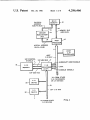
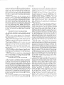
13 Claims, 18 Drawing Figures
size;
£01K e2
BUStP? BUS) 2
E
‘5
MEMQ'RY
‘1i:
MANQGEHENT
venom aus
U‘EM BB5}
UNIT
I4
W
"jg
PROCESSOR
~
LOGICAL ADDRESS
BUS {LA BUS}
aosr
1/0
HGST
Cumsouen
l/O BUS
1GP CONTROL
SIGNALS
xoP MEM Bus /|1
m
w
\J
)
10?
e ENPERQUPT CQDE SIGNALS
I ,6
umoav
*' eaocessea
- cars
{1GP}
/
‘C?PtSDLE SIGNALS
10F‘ ADD BUS
%
$701 FKJMVOTHER
1/0
20“ on“:
I10 PROCESSORS
on to oevlcis
as
no
20v some I:
I
1
we no so;
iii
TO #FROM OYHER
I I O DEVPCES
US. Patent
062. 20, 1981
4,296,466
Sheet 1 of 8
PHYSiCAL
ADDRESS
Mm"
MEMO RY
BUSiPA BUS) )
,2
1
&
7
l6
*5
MEMORY BUS
MEMQRY
1E3
MANAGEMENT
(MEM BUS)
mm
4
1;4
HOST
/
/’ ‘0
paoczssoa
000ml. ADDRESS
A
BUSiLA sass}
'
~
“
HOST
1/0
HOST
CONTROLLER
1 x0 BUS ~__
IOP CONTROL
SIGNALS
IQ? MEM BUS
'
l7
—' iNTERRUPT CODE SlGNALS
:0P
MEMORY
:—
.-_ DATA
CO NSOLE SiGNALS
10p ADD BUS
1
TO/ FROM own
I /0 PROCESSORS
GR 1/0 DEVICES
I ,0
20v
DEVICE
‘
~49
1/0
20 v
ozvace
I
- IOP 1/0 BUS
\~
:1:
TO /FROM OTHER
I /O DEWCES
FIG!
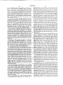
US. Patent
06:. 20, 1981
Sheet 5 of 8
4,296,466
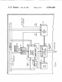
H1 IORST
(FROM HOST)
SYSCLK
A
_/ 52
SLAVE SELECT
L 51
SDATOB
-
J
Q
K
5 /
--—o CLK
\ STRT
arms MATCH
3-;
SV.
rJ
53
---
H TRACE
(FROM HOST)
5-,
10p MATCH
.-
CLR MAP m1,
s-an
HRBUF . COMPAR
-'r*
____.
‘
33 37
{FROM HOST) “LP
ATQR
1-»
ENAB
J
-/
L 56
-
'
H EXT cows.
HINTR
—
(TO HOST STATE
CHANGE were}
5v.
;
CLR MAPINT
50
1
=1,
I
SI/OPLS -—JCLK5 0
e-Bn
SLAVE
M58
_
SL AVE SELECT
ID
‘T’ 6932R-
DStD-DSS
|
{FROM 1/0
1
DEVICE) -1—>
—
R Q
s9
SSELD
1’
SICRST
sLKvE SELECT
HRQENB
(FROM HOST}
H‘NTR
-‘——-J Q
(FOR STANDARD
INTERRUPT
)
CLK
55v
6
F165
0
54
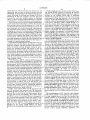
US. Patent
061. 20, 1981
Sheet 6 of8
4,296,466
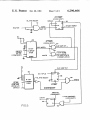
I
i
l
FETCH INSTRUCTTON
l
E XECUTE iNSTRUCTlON
l
4—-——- ASSERT IOP
FETCH DATA
INTERRUPT
1
EXECUTE DATA
MANIPULATION
I:
T
F ETCH N EXT INSITRUCT ION
|
SAVE
INSTRUCTION
RETURN TO
I
‘
MAIN
EXECUTE NEXT
PROGRAM
ENSTRUCTION
T
l
ACCESS ROM
ADDRESS 4
MATN PROGRAM
ROUTINE
‘
H EXT COND [FROM I6?)
RETURN TO
MAIN
PROGRAM
ASSERTED
9
TRUE
NOT ASSfRTED
FALSE
MiCRO-INTERRUPT
MICRO-INTERRUPT
ACCESS MICRO
PERFORMNQRMAL"
mTsRRuPT
M ICRO 4:005
INSTRUCTTON
EXECUTE MEMORY
INTERRUPT
PROGRAM
ROUTiNE
(LOSES SAVED
WSTRUCUON)
RE -ALLOCATION
ROUTiNE
ASSERT HTRACE
———- T0 snow
MAPIS LOADED
T
TO IOP
,
V
F ‘G. 6
1
4,296,466
DATA PROCESSING SYSTEM INCLUDIN‘G A
SEPARATE INPUT/ OUTPUT PROCESSOR WITH
MICRO-INTERRUPT REQUEST APPARATUS
INTRODUCTION
This invention relates generally to data processing
systems and, more particularly, to such systems which
utilize a separate input/output (I/O) processor for corn
municating between a host processor and one or more
peripheral I/O devices.
2
terrupt processing which must occur in the host procc»
sor is not nearly as extensive as it wouid be if the host
processor were dealing with the U0 devices directly,
there is still a certain amount of interrupt processing
time that must be used by the host processor in order to
define the extent ofthe interrupt service which has to be
performed. It is desirable to minimize the processing
time that the host processor must use for such purpose
so that it can return to its normal operations as quickly
as possible, even when using a separate I/O processor.
Further, if more than one I/O processor is used on
the host I/O bus,‘a priority among them must be estab
BACKGROUND OF THE INVENTION
lished with respect to use of the host I/O bus. For exam<
In most conventional data processing systems, com
munication between a central, or host, processing unit
ple, if an I/O Processor is performing a Read-Modify
Write operation such processor must inform all other
processors that such operation is occurring so that the
I/O processor performing such operation can complete
the operation before the host I/O bus becomes available
to all other I/O processors.
and one or more peripheral I/O devices, such as large
capacity storage devices of the tape or disc type, display
devices, card readers, and the like, is normally achieved
by means of an I/O bus to which all of the I/O devices
have access. Normally when access to the host proces
sor or to the host main memory is required by an exter
nal I/O device, the latter device must generate an “in
terrupt" signal which must then be appropriately pro
cessed by the central processor unit to identify the I/O
unit and to determine what operation the interrupting
unit requires the host processor to perform. The host
processor must stop its operation, i.e. interrupt its pres
ent machine state, in order to process the interrupt
signal. That is, the host processor must identify the
interrupting device, must perform whatever data han
dling is required, and must restore the host processor to
its previous machine state so that it can resume the
operation it was performing prior to interruption. The
processing of such an interrupt signal normally requires
BRIEF SUMMARY OF THE INVENTION
In accordance with the invention, the system utiiizes
an auxiliary I/O processor. separate from the host pro
cessor, the host processor being capable of interruption
by the U0 processor. When interrupted the host pro
cessor accesses a speci?cally designated micro-program
location and asserts a special code bit combination {re
ferred to as the “external condition" code) which corre
sponds to a special form of interrupt, referred to herein
as a “micro-interrupt” in contrast to a standard, or nor
mal, interrupt condition used in presently available
systems. During a micro-interrupt, the I/O processor
requires a re-allocation of the contents of a memory
allocation, (Le. a memory address translation) unit, re
a relatively long time period before the processor is 35 ferred
to as a MAP unit, thereof. Once a MAP unit has
ready to resume its previous operation.
been appropriately re-allocated data can be transferred
In order to avoid the excessive time required for such
directly between the I/O processor and the host main
interrupt processing, it has been suggested that a sepa
rate processor unit, commonly designated as an I/O
processor, be utilized as an intermediary between exter
nal 1/0 devices and the main, or host, processor unit.
Such I./O processor is normally provided access to the
host I/O bus and, in turn, has its own I/O bus to which
access can be obtained by one or more peripherai {.19
memory via the MAP unit without the need for further
processing time on the part of the host processor.
If the I/O processor is requesting a micro-interrupt,
upon receipt of the externai condition coded bit combi
nation it compares such code to a fixed code which
represents a micro-interrupt condition and asserts an
devices. In such a way the I/O processor performs the 45 external condition signal (HEXT COND} which is
transferred to the host processor and indicates that the
processing which is required when an interrupt signai is
transmitted from an I/O device so that the main or host
processing unit is not required to stop its operation for
such interrupt signal processing. The {/0 processor
thereupon takes care of the transfer of data to or from
the I/O device and, thence, to or from the main proces
sor unit or the main memory of the host machine. The
host is being interrupted by a “true” micro-interrupt
from the I/O processor. Once the host processor identi
ties the interrupt request as a micro-interrupt request,
the host accesses a micro-interrupt routine at a speci?ed
location in a read-'only-mernory (ROM) of the host
processor and performs the necessary steps providing
for the desired MAP re-allocation, the data which spec
ii'ies the re-allocation being in the host main memory.
ulations oniy, which manipuiations can be achieved at
the host processor high speed of operation, the data 55 If the I/O processor is requesting a normal interrupt,
rather than a micro-interrupt, the host processor pro»
transfer to and from the I/O devices being handled by
cesses the interrupt in an appropriate manner as would
the separate l/O processor.
host processor then merely handics the U0 data manip’
The 1/0 processor often has its own local memory,
be well-known to those in the art. using c. inrieyer pro
cessing time is normally required on the part ot' the host
vides for the storage of programs for processing inter 60 processor. In contrast, once a micro-interrupt process
has been instituted and the re-aliocation has been com
rupts and for the local storage of data before transfer
piete, data transfer is controlled directly by the I/O
either to or from the host processor or to or from the
processor without the need for such further host pro
1/0 device.
cessing tire- 3 he use of a micro-interrupt process
In such presently used systems, the I/O processor
thereby pro‘. lLlL‘» u mechanism by which an I/O proces<
must interrupt the host processor (in effect, on behait" of
sor can provide a fast and efficient data transfer. Once
the I/O devices), to provide a particular memory allo
the host processor has identified the interrupt request as
cation which is required by the I/O processor or by the
a micro-interrupt it can immediately and automatically
IOP I/O devices utilizing host memory. While the in
usually of relatively iow storage capacity which pro
3
4,296,466
access previously stored data for providing the desired
memory rc~allocation without the need to perform its
normal. more time-consuming software interrupt han~
dling routine. The U0 processor can communicate
directly with the host memory while the host processor
performs its own operation in a manner which permits
4
by Data General Corporation. Southboro. Mass. Such
data processor system and its operation is described, for
example. in the publicno-iina “User! Manual Program
mer‘s Reference. Zciipsc
Line
01 5-000024. with specific reference to the writable con»
trol store aspect thereof. in the publication "User‘s
it. in effect. to ignore such [/0 processor/host memory
Manual Programmer’s Reference. 5/130 Micro Pro
communication.
gramming WCS Feature". DIS-000069, and "User's
Further. in accordance with the invention, an I/O
Manual, Interface Designer’s Reference Nova and
processor which is performing a Read-Modify-Write . . O Eclipse @ Line Computers". 0154100031. such public-(1'
operation ('i.e.. reading the contents of a speci?ed loca
I tions copyrighted and published by and available from
tion in the host main memory. modifying such contents,
Data General Corporation. Since. in accordance with
and rewriting the modified contents into the same loca
such publications, the structure and operation are
tion) asserts a special signal which prevents any other
known to the art. the system need not be described in
I/() processor which may be connected to the host I/O 5 further detail here.
bus from gaining access to any location in main memory
The U0 processor and I/O processor memory are
until such Read—Modify-Write (RMW) operation has
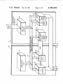
shown in further detail in the block diagram of FIG. 2.
been completed. In effect, the I/O processor which is
performing the RMW operation overrides the operation
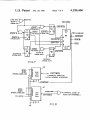
In effect. the processor can be described as comprising
a first central processor unit on processor board 25
of all other [/0 processors on the host I/O bus so that
which unit comprises control logic 26 and computation
no other I/O processor can obtain access to the host
processor.
logic 27 and an appropriate logical address bus 28 for
transferring addresses among the various I/O processor‘
DESCRIPTION OF THE DRAWINGS
units and a memory bus 29 for transferring data there
arnong. Appropriate I/O interface logic 30 is included
A preferred embodiment of the invention can be 25 for communication with [/0 devices via the IOP I/O
described with the help of the accompanying drawings
bus 19. Communication with the host processor is
wherein:
achieved by other logic circuitry on a second processor
FIG. 1 shows a block diagram of an overall data
board 31 which includes a state change logic and con
processing system using an I/O processor in accordance
trol store unit 32 (described in more detail with respect
to FIG. 3) and appropriate interface logic 33 for com~
with the invention;
FIG. 2 shows a block diagram of the [/0 processor of
municating with the host processor via the host I/O bus
FIG. 1;
II.
FIGS. 3 and 4 show block diagrams of portions ofthe
The ID? memory is also placed on board 31 and
I/O processor of FIG. 2;
includes the local memory 18 and a memory manage
FIG. 5 shows a block diagram of speci?c logic used 35 ment unit (MAP) 60 for providing memory allocation as
in the “micro-interrupt” process in accordance with the
invention;
FIG. 6 shows a flow chart of the steps which occur
during a micro-interrupt of the host processor by the
[/0 processor;
FIGS. 7 and 8 show a block diagram of specific logic
discussed in more detail with respect to FIG. 4. The
IOP I/O bus is supplied to the memory allocation unit
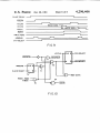
as shown in FIG. 2. The state change logic and control
store as shown in FIG. 3 includes state change logic unit
the I/O processor local memory or to the host proces
34, control store unit 35, a ROM buffer register (RBUF)
36, and a register 37 for identifying the current page
being accessed in control store. The state change logic
unit 34 communicates with other units of the I/O pro
sor memory;
cessor via memory bus 29 and the output of RBUF unit
used in determining whether a memory reference is to
FIGS. 9 and 10 show, respectively, a timing diagram 45 36 provides an RBUF signal to the control logic 26 on
and a block diagram of the logic used in preventing
V0 processor board 25, a portion of such signal.
access to the host memory during a read-modify-write
namely, RBUF bits 32-35 being supplied also to state
change logic unit 34.
operation by the I/O processor.
DESCRIPTION OF THE INVENTION
The memory and MAP unit 18 of the I/O processor
is shown in FIG. 4 and includes the [/0 processor local
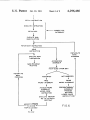
FIG. 1 shows an exemplary system in which the
memory which includes memory parity logic 41. Data
invention is used. As can be seen therein a host proces
sor 10 has a host I/O bus 11, for communication with
is supplied to local memory 40 from the memory bus 29.
the memory parity bit being supplied to memory parity
logic 41 via parity generator unit 42. Data is supplied
appropriate I/O devices, and a main memory 12, the
allocation of addresses being supplied to the main mem 55 from the local memory to the memory bus 29 as shown.
In accordance with standard practice the memory has a
ory being appropriately managed by a memory manage
ment unit 13 which converts logical addresses received
memory address control unit 43 for supplying addresses
thereto via the logical address bus 28. The memory is
on logical address bus 14 into physical addresses in the
refreshed periodically in accordance with refresh
main memory as supplied thereto on physical address
bus 15. Data to and from the main memory are trans
ferred on memory bus 16. An [/0 processor 17, as
counter unit 44 in a manner well known to those in the
art. Control logic for controlling the parity detection
and the MAP/timer operation, as well as providing
discussed above. communicates with the host processor
logic to interface with the IOP l/O bus. is shown by
on the host i/C) bus 11, has its own local IOP memory
unit 45. The memory allocation is appropriately deter
18. and communicates with I/O devices 20 on its own
65 mined by the I/O processor window MAI’ unit 47
IOP I/O bus 19.
which controls whether the processor is to access the
In a preferred embodiment of the invention the host
local memory (when the EXT PMCZ signal is asserted]
processor and the I/() processor are of the Eclipse@
or the llttst memory win the liost?lOl’ interface tuhrn
type known to those in the art as manufactured and sold
5
4,296,466
the INT PMCZ signal is asserted), as discussed in
greater detail below. As discussed above in general
terms, a key feature of the invention herein lies in the
ability to interrupt the host processor in a way which
reduces the processing overhead time of the host pro
cessor and effectively permits direct control of the host
memory allocation. Such interrupt is de?ned, as de
scribed above, as a “micro-interrupt“ process, the oper
ation of which is best described with the help of the
logic shown in FIG. 5.
To initiate the micro-interrupt operation the I/O
6
HRBUF 33-37 match the ?xed 5 bits {representing the
IOP state change external condition code) at the com
parator 53 in the I/O processor and if the interrupt
(signi?ed by an H)? MATCH signal) has been synchro
nizcd at AND gate 56 with the HiNTR signal from D
flip-flop 55, the HEXT COND is asserted and supplied
to the host processor from the I/O processor to signify
that the I/O processor is requesting a micro-interrupt.
The host processor recognizes the assertion of the
HEXT COND signal from the I/O processor as a true
micro-interrupt and thereupon selects the true address
for the micro-interrupt operation. The test to determine
whether the interrupt is a true micro-interrupt is per
(identi?ed as the DOB ac, 4/ instruction) which asserts
tormed at a designated rnicroprogrant location in the
an SDATOB signal. The six least signi?cant bits of the
instruction (such bits are referred to as the “device t. . 5 interrupt handling microcode oi the host processor.
processor must execute a speci?ed instruction therefor
code“ and are identi?ed in FIG. 5 as SLAVE osp
DSS) are compared with a ?xed 6-bit code (represent
when such a true micro-interrupt occurs, the host
processor accesses, front a itnown location in the main
memory, the pointer to the data which identi?es how
ing device code 4) at comparator 50. If the SLAVE
many changes are going to be made in the MAP, which
DSdi-DSS bits match the ?xed “device code 4” bits,
2.6 MAP is to be changed, and the data for the change. The
comparator 50 asserts a SLAVE SELECT signal.
host then transfers the data block from memory into the
The assertion of SDATOB and SLAVE SELECT
data channel MAP so that the MAP is then available for
provides 21 START MAP INT signal at the output of
translating logical addresses received from the request
AND gate 51. Such signal is supplied to a }-K flip-flop
ing I/O processor into physical addresses in the host
unit 52. Flip-?op 52 provides at its Q output a signal for
OR gate 54 (at the bottom of FIG. 5) when a micro 25 main memory.
When the selected host data channel MAP unit has
interrupt is being requested. OR gate 54 also has an
had its contents so changed to provide for the host
input which indicates when a standard interrupt is being
memory re-aliocation, the host sends an appropriate
requested, the logic for such standard interrupt indica
indication thereof, i.e., the HTRACE signal, which as
tion being well known and, for the purposes of describ
shown in FIG. 5 is supplied to gate 57 together with the
ing the invention herein, will not be discussed in further
IOP MATCH signal from comparator 53. The latter
detail here.
signal again arises from a second comparison of the
The output of OR gate 54 is supplied to a D ?ip-?op
HRBUF bits 33-37, supplied thereto from the host,
unit 55 which is periodically clocked by a host RE
with the ?xed bits at comparator 53. When the
QUEST ENABLE signal (HRQENB) in accordance
with the standard host I/O interface logic. D tlip-?op 35 HTRACE signal and the It)? MATCH signal are as
serted, the CLR MAP INT signal from gate 5? indi
55 thereupon produces a signal indicating to the host
cates that the selected data channel MAP has been
that an interrupt is being requested by the I/O proces
sor, such signal identi?ed as the HINTR signal.
It is helpful at this point in understanding the micro
interrupt operation to review the operation of a known
host processor of the Eclipse type as mentioned above.
As is known the host processor is of the micro-pro
grammed type and includes state change logic which
determines the next micro-address in the host ROM for
the host processor’s next micro-instruction, such deter 45
mination being implemented throuh a 6-bit ?eld (identi
loaded with its new contents. The CLR MAP INT
signal is supplied to the J input of .I-K flip-flop 52 to
disable the comparator‘ 53. The CLR MAP INT signal
is also supplied to a flag ?ip-?op 58 (a D ?ip-?op cir
cult), the Q output of which is supplied to gate 59 to
gether with the SLAVE SELECT signal to produce an
S SELD signal which indicates to the U0 processor
that the memory re-allocation in the selected MAP unit
of the host processor has been completed as required.
The 6-bit ?eld speci?es a test for selecting a “true" or a
“false” address as the address for the next micro
At such point the host MAP status (not the MAP
contents) in the host is restored, the capability for re
ceiving interrupts by the host processor is again re
?ed as HRBUF 32—37) in the current micro-instruction.
instruction. Selected state change codes of the host
stored, and the host processor can continue its own
processor (e.g., in the Eclipse processor, the state
change codes 40-77) represent external condition state
change codes, one of the bits of the above 6-bit ?eld
program operation without further processing or com
the ENAB MATCH signal from 1-K flip-flop 52. If
from the [/0 processor then occurs between the time in
munication being required between the host processor
and the I/O processor.
Accordingly, the micro-interrupt process, as de
(HRBUF 32) being asserted for such external condition
scribed
above avoids the processing time that the host
55
state change codes.
processor normally must perform in order to process a
The test performed with reference to the external
standard or normal interrupt. It is helpful in this connec
condition state change codes by the host is the sampling
tion to consider the relationship of the micro-interrupt
of the HEXT COND signal. When an external state
change code is present and the HEXT COND signal is ' operation with reference to the steps of a program being
asserted, the true address is selected as the address for 60 performed by the host processor, as shown in FIG. 6.
Thus, the host processor, in the course of performing
the next micro-instruction. If the HEXT COND signal
programmed steps, fetches an instruction, executes the
is not asserted in the presence of an external condition
instruction, tetches data in response thereto. and then
code, the false address is selected. HRBUF 32 indicates
executes whatever data manipulation is required before
the presence of an external condition state change code
and HRBUF 33-37 specify a device which the host 65 fetching the next instruction. Such process is a conven
tional process performed by a central processor unit in
selects to be tested.
performing a program. The assertion of an interrupt
Thus, as seen in FIG. 5, comparator 53 is enabled by
7
4,296,466
8
which the host central processor unit fetched the last
instruction and the time at which it fetches the next
FIGS. 7 and 8 show the speci?c window MAP logic.
The USER MODE signal at D flip-flop 64 indicates
instruction. In accordance with standard interrupt pro
cesses following the fetching and saving of the next
instruction of the host program, the host processor
decision by the window MAP logic to determine
whether or not a program memory reference requires a
whether the program reference is for the I/O processor
accesses the read only memory address, as discussed
local memory or the host memory via the host/IOP
interface. Ifthe USER MODE signal is not asserted the
an interrupt is a normal interrupt or a micro-interrupt.
program reference automatically is determined to be a
If the [/0 processor provides a HEXT COND signal
local memory reference, while if USER MODE is as
(as discussed above with reference to FIG. 5) so that the 0 serted the window MAP logic determines whether the
host processor knows that the interrupt is a "true” mi
local memory interface is to be inhibited from starting
cro-interrupt the host processor thereupon accesses the
(INT PMCZ is asserted at RAM 66) or the host/IOP
micro-interrupt micro-code instruction which permits
interface is to be inhibited from starting (EXT PMC2 is
the execution of the memory re-allocation routine for
asserted at RAM 67). The DCH ADDR signal distin
changing the contents of a selected data channel MAP.
guishes whether the reference is a program reference
Once the MAP contents are appropriately re-allocated
(DCH ADDR is not asserted) or a data channel refer
(loaded), the host processor asserts its HTRACE signal
ence (DCH ADDR is asserted). The operation with
to show such condition and supply such signal to the
respect to a data channel reference (DCH MODE) at D
l/O processor. The host processor can then return to its
flip-flop 65 is similar to that with respect to the program
above, so that it can make a determination as to whether
own main program to execute the next instruction that
had been previously fetched and saved, thereupon re
turning to its main program routine.
Ifthe HEXT COND signal is not asserted by the I/O
processor, the host then knows that there is a normal
interrupt condition. The host processor thereupon per
reference (USER MODE).
If the memory reference is for the host memory, since
there are four MAPs in the host processor which can be
used for translating logical addresses into physical ad
dresses in the host memory, two additional bits must
25 accompany the normal 15 address bits to identify which
forms its normal interrupt program routine in accor
dance with standard practice well known in the art.
of the four host MAPs is to be used. Such bits are ob
tained at multiplexer 63 and identified as DCHLAti) and
Following the normal interrupt program routine the
XDCH. If an I/O device on the I/O processor I/O bus
host processor thereupon returns to the main program
requests a data channel access, it provides l5 bits of
but because of the need for the host processor to use its 30 address as 1/0 processor data bus SDATAl-IS and the
own internal registers in a normal interrupt, the previ
two map select bits as SDATA¢ and SEXT DCH.
ously saved instruction has been lost and it must again
SDATAl-IS are provided to the window MAP when
fetch the next instruction before it can resume its own
DCH ADDR is asserted as logical address bits 1-15,
main program routine.
and SDATAd) as SALUd) OUT. SALU¢ OUT is sup
With reference to FIG. 5, when the S SELD signal at 35 plied from multiplexer 63 as DCHLAq‘), and subse
the output of logic 59 has been flagged to indicate that
quently is sent to the host as bit (I) of the host‘s I/O bus.
the micro-interrupt process has been completed by the
SEXT DCH is supplied from multiplexer 63 as XDCH
host processor, the I/O processor software is devised to
test the flag condition so that when it is determined that
at the output thereof, and is subsequently sent on to the
host as EXTERNAL DCH. Ifthe program supplies the
logical address (a program reference), the two bits re
quired for identifying the MAP are obtained as
the micro-interrupt processing has been completed (by
the presence of the S SELD signal) the [/0 processor
software can then proceed to perform the desired data
transfer routine for which the interrupt was originally
requested. The transfer of data to and from the host
memory via the host [/0 bus and the host/IOP inter
UXDCH and UDCHO at the multiplexer from D flip
flops 68 and 69.
As mentioned above, if the [/0 processor is reading
45 the contents of a speci?ed location in the host main
face 33 (see FIG. 2) is performed by appropriate logic
memory, modifying such contents, and re-writing the
which is well known to those in the art and, accord
modified contents into the same location, a Read-Modi
ingly, the host/IOP interface unit need not be described
fy-Write (RMW) operation, other [/0 processors must
in more detail. For the purpose of such data transfer the
I/O processor, in effect, acts as an I/O device with
be prevented from gaining access to that same host
memory location until the RMW operation is com
reference to the host and requires the standard interface
pleted. Such capability is provided by the assertion of a
RMOD PENDING signal by the I/O processor which
is performing the RMW operation. As long as the
RMOD PENDING signal is asserted then the particu
control logic normally used for transferring addresses
and data to the host from an external [/0 device in a
manner well known to those in the art.
In FIG. 2 the window MAP unit 60, associated with 55 lar I/O processor performing an RMW operation is
the I/O processor local memory unit 18, determines
uninterruptable, even by a higher priority l/O proces
whether the I/O processor is to access the IOP local
memory 18 or is to access the host main memory 12 via
sor.
the host l/O bus 11. Accordingly, the window MAP
unit 60 acts as an I/O processor memory management
of FIG. 10 are helpful in understanding such operation,
The logic diagram shows, in effect, the standard data
unit for providing operation either with respect to the
channel interface to an Eclipse® processor from the
local memory or with respect to the host memory. The
MAP unit 60 provides operation in two modes, "user"
I/O processor except for modification required with
respect to the RMOD and RMOD PENDING signals,
mode and “data channel" mode, either one of which
The RMOD signal is internally generated by the I/O
The timing diagram of FIG. 9 and the logic diagram
can be “on" or “off” in any combination thereof, as 65 processor for providing the RMOD PENDING signal
indicated by the signals USER MODE and DCH
MODE from ?ip-?ops 64 and 65, respectively, in FIG.
which is supplied externally thereto to inform all other
[/0 processors that they cannot respond to the data
7.
channel control signals HDCHA, HDCHO, and
9
4,296,466
16
to said host processor for identifying said interrupt
HDCH! until the cycle following the "re-write" opera
tion of the asserting I/O processor. The SLAVE
READY signal is also generated internally by the I/O
processor and signi?es that the I/O processor is request
request as one requiring the re-allocation of said
selected portion of the contents of said memory
management unit, whereby said host processor can
perform such re-allocation in accordance with a
speci?ed program in its micro-program control
store;
ing a data channel access to the host. In accordance
with standard Data General Corporation interface
logic, this causes the HDCHR signal to be asserted at
gate 74 at the time the HRQENB signal clocks flip-flop
said input/out processor thereby being capable of
73. The 1/0 processor will then respond to the host data
accessing said host memory and said memory man
agement unit via said input/output bus means for
the direct transfer of logical addresses to said re
channel acknowledge signal (HDCA) by asserting the
HOST DCHA signal and the DCH SELECT signal, if
the host data channel priority in signal (HDCHPIN) is
allocated selected portion of said memory manage
ment unit and for the direct transfer of data be
tween said input/output processor and said host
The timing diagram shows the relationship among
memory when said selected portion of said mem
the host data channel request signal (HDCHR), the host
ory management unit has been re-aliocated.
request enable signal (HRQENB), the host data channel
2. A data processing system in accordance with claim
acknowledge signal (HDCHA), the host data channel
I wherein said input/output processor has an instruc
output and input signals (HDCHO and HDCHI), the
tion register containing an instruction and said micro
RMOD signal and the RMOD PENDING signal. Such
host signals (HDCHA, HDCHR, HDCHO, HDCHl, 20 interrupt identifying means includes
?rst logic means responsive to a ?rst ?xed coded
HRQENB) are of the type used in the Eclipse @ pro
signal and to a coded portion of said instruction
cessor, as discussed in the above referred to publications
also true.
thereon, particularly in the Interface Designer's Refer
ence Manual. The RMOD and RMOD PENDING
signals are asserted after assertion of the HDCHO signal 25
(i.e., while the data is being read) and lasts until after the
assertion of the i-IDCHI signal (i.e., while the modi?ed
signal from said instruction register for providing a
?rst matching signal when said ?rst ?xed coded
signal and said coded portion of said instruction
signal match; and
second logic means responsive to said ?rst signal and
to said micro-interrupt request signal for providing
data is being re-written). During such time period an
other I/O processor cannot respond to the HDCHA
signal until the next cycle following the non-assertion of 30
RMOD PENDING, i.e., the cycle following the “re
write” of the ?rst processor once the data has been
modi?ed. This is because RMOD of the non—asserting
I/O processor will be false, with RMOD PENDING
true. The output of gate 70 will thus be low forcing the 35
output of gate 71 high and the output of gate 72 low, as
if the non-asserting I/O processor were not requesting a
data channel access of host memory, regardless of the Q
a second signal indicating that a micro-interrupt
has been requested.
3. A data processing system in accordance with claim
2 wherein said micro-interrupt identifying means fur
ther includes
second means responsive to a second ?xed coded
signal and to said speci?ed coded signal from said
host processor to provide a second matching signal
when said second ?xed coded signal and said speci
?ed coded signal match;
output of flip-flop 73. The non-asserting processor will
means responsive to said second signal and and to a
thus not assert its DCH SELECT signal or its HOST 40
periodic signal from said host processor to provide
an internal interrupt signal;
means responsive to said second matching signal and
to said internal interrupt signal for providing an
external condition signal to said host processor
indicating that the interrupt request is a true micro
DCHA signal at the time that the HDCHA signal initi
ating the rewrite cycle in the asserting processor is
received. Moreover, the non-asserting processor will
not force the channel priority out signal
(HDCHPOU’D high.
45
What is claimed is:
l. A data processing system comprising a host proces
interrupt request.
4. A data processing system in accordance with claim
3 wherein said input/output processor further includes
sor having a microprogram control store, a host proces
means responsive to a signal provided by said host pro
sor memory, and a host memory management unit, the
contents of which permit the conversion of logical ad 50 cessor when the re-allocation of said selected portion of
said memory management unit has been completed for
dresses received by said host processor into physical
providing a signal to the input/output processor control
addresses for said host memory, and further comprising
logic means to indicate that said re-allocation has been
an input/output processor;
completed.
input/output bus means for providing communica
5. A data processing system in accordance with claim
tion between said input/output processor and said
1 wherein said input/output processor has a local mem
host processor, said host processor being capable of
ory and further includes
generating a speci?ed coded signal in response to
window map means for selectively providing access
any interrupt request from said input/output pro
said input/output processor including
to said local memory or to said host processor
memory in accordance with a selected memory
means for generating a micro-interrupt request signal
reference signal, said window map means compris
cessor;
for said host processor to request a re-allocation of
a selected position of the contents of said memory
management unit; and
micro-interrupt indentifying means responsive to said 65
speci?ed coded signal received from said host pro
cessor and to said micro-interrupt request signal of
said input/output processor for providing a signal
ing
multiplexer means capable of being responsive to
either a program memory reference signal or a data
channel memory reference signal and further re
sponsive to a memory reference identifying signal
which selects which of said memory reference
signals the multiplexer means is responsive to, said
i
g
11
4,296,466
12
?rst input/output bus means for providing communi
cation between said input/output processor and
host processor;
second input/output bus means for providing com—
munication between said input/output processor
multiplexer means thereby selectively providing an
enabling signal which depends on the state of the
memory reference signal to which said multiplexer
means responds; and
inhibit logic means responsive to the selective provi
sion of said enabling signal and to said memory
reference identifying signal for inhibiting access
and one or more devices external to said input/out»
put processor;
said input/output processor including
either to said local memory or to said host proces
sor memory depending on whether the memory
reference is to said local memory or to said host
processor memory.
a local memory;
a logical address bus in said input/output processor
for providing logical addresses for said local mem
ory or said host memory; and
window map means connected to said logical address
6. A data processing system in accordance with claim
5 wherein said inhibit logic means includes means for
bus for selectively providing access by said input
providing a first inhibit signal for inhibiting the start of
the interface of said input/output processor and said
/output processor or by said one or more external
devices to said local memory or to said host proces
sor memory in accordance with a selected memory
local memory when the memory reference to to said
reference signal, said window map means compris
host processor memory and means for providing a sec
ond inhibit signal for inhibiting the start of the interface
of said input/output processor and said host processor 20
when the memory reference is to said local memory.
ing
multiplexer means capable of being responsive to
either a user mode signal generated by said input—
/0utput processor or a data channel mode signal
7. A data processing system in accordance with claim
generated by said input/output processor and fur
6 wherein said host memory management unit has a
ther responsive to a memory reference identifying
plurality of memory allocation units and said multi
signal generated by said input/output processor
plexer means is further responsive to a selected one of
two sets of bits depending on whether the memory
channel mode signals the multiplexer means is re
which selects which of said user mode or data
sponsive to, said multiplexer means thereby selec
tively providing a window map enabling signal
reference is a program memory reference or a data
channel memory reference for providing an output set
of bits for identifying a selected one of said plurality of
which depends on the state of the selected user
mode or data channel mode signal to which said
memory allocation units, said output set of bits being
multiplexer means responds; and
supplied to said host processor as an extension of the
inhibit logic means comprising random access mem
ory means responsive to said window map enabling
logical address for said memory reference.
8. A data processing system in accordance with claim
7 wherein each of said two sets of bits comprises a pair
signal, to said memory reference identifying signal
and to address bits from said logical address bus for
inhibiting access by said input/output processor or
of bits and said output set of bits is a pair of bits for
identifying one of four of said plurality of memory
allocation units.
9. A data processing system in accordance with claim
1 wherein said input/output processor further includes
means for preventing any other processor from access
by said one or more external devices either to said
local memory or to said host processor memory
depending on the contents of said random access
claim 9 wherein said access preventing means includes
said host processor memory and means for providing a
means for generating an access inhibiting signal which
starts when the data in said host processor memory is
second inhibit signal for inhibiting the start of the inter
face of said input/output processor and said host pro
memory means.
12. A data processing system in accordance with
ing said host processor memory when said input/output
claim 11 wherein said inhibit logic means includes
processor is performing a read-modify-write operation
means for providing a first inhibit signal for inhibiting
45 the start of the interface of said input/output processor
with respect to data in said host processor memory.
and said local memory when the memory reference is to
10. A data processing system in accordance with
cessor when the memory reference is to said local mem
cry.
being read by said input/output processor and ends
when the modi?ed data is being rewritten into said host
processor memory, said access inhibiting signal being
supplied to other input/output processors on the host
input/output bus means to prevent other processors
13‘ A data processing system in accordance with
claim 12 wherein said memory management unit has a
plurality of memory allocation units and said multi
plexer means is further responsive to a selected one of
two sets of bits depending on whether the memory
from obtaining access to the location in said host mem
ory at which said data is being read, modi?ed and re
written.
11. A data processing system comprising a host pro
cessor having a microprogram control store, a host
memory and a host memory management unit and fur
channel memory reference for providing an output set
of bits for identifying a selected one of said plurality of
ther comprising
logical address for said memory reference.
reference is a program memory reference or a data
memory allocation units, said output set of bits being
supplied to said host processor as an extension of the
*
an input/output processor;
65
1i‘
1K
*
lit