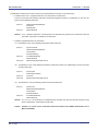
1
User’s Manual
QB-V850ESJX3H
In-Circuit Emulator
User’s Manual
Target Devices
V850ES/JC3-H
V850ES/JE3-H
V850ES/JG3-H
V850ES/JH3-H
V850ES/JG3-U
V850ES/JH3-U
V850ES/ST3
All information contained in these materials, including products and product specifications,
represents information on the product at the time of publication and is subject to change by
Renesas Electronics Corp. without notice. Please review the latest information published by
Renesas Electronics Corp. through various means, including the Renesas Electronics Corp.
website (http://www.renesas.com).
www.renesas.com
Rev.4.00
Dec, 2012
Notice
1.
2.
3.
4.
5.
6.
7.
All information included in this document is current as of the date this document is issued. Such information, however, is
subject to change without any prior notice. Before purchasing or using any Renesas Electronics products listed herein, please
confirm the latest product information with a Renesas Electronics sales office. Also, please pay regular and careful attention to
additional and different information to be disclosed by Renesas Electronics such as that disclosed through our website.
Renesas Electronics does not assume any liability for infringement of patents, copyrights, or other intellectual property rights
of third parties by or arising from the use of Renesas Electronics products or technical information described in this document.
No license, express, implied or otherwise, is granted hereby under any patents, copyrights or other intellectual property rights
of Renesas Electronics or others.
You should not alter, modify, copy, or otherwise misappropriate any Renesas Electronics product, whether in whole or in part.
Descriptions of circuits, software and other related information in this document are provided only to illustrate the operation of
semiconductor products and application examples. You are fully responsible for the incorporation of these circuits, software,
and information in the design of your equipment. Renesas Electronics assumes no responsibility for any losses incurred by
you or third parties arising from the use of these circuits, software, or information.
When exporting the products or technology described in this document, you should comply with the applicable export control
laws and regulations and follow the procedures required by such laws and regulations. You should not use Renesas
Electronics products or the technology described in this document for any purpose relating to military applications or use by
the military, including but not limited to the development of weapons of mass destruction. Renesas Electronics products and
technology may not be used for or incorporated into any products or systems whose manufacture, use, or sale is prohibited
under any applicable domestic or foreign laws or regulations.
Renesas Electronics has used reasonable care in preparing the information included in this document, but Renesas Electronics
does not warrant that such information is error free. Renesas Electronics assumes no liability whatsoever for any damages
incurred by you resulting from errors in or omissions from the information included herein.
Renesas Electronics products are classified according to the following three quality grades: “Standard”, “High Quality”, and
“Specific”. The recommended applications for each Renesas Electronics product depends on the product’s quality grade, as
indicated below. You must check the quality grade of each Renesas Electronics product before using it in a particular
application. You may not use any Renesas Electronics product for any application categorized as “Specific” without the prior
written consent of Renesas Electronics. Further, you may not use any Renesas Electronics product for any application for
which it is not intended without the prior written consent of Renesas Electronics. Renesas Electronics shall not be in any way
liable for any damages or losses incurred by you or third parties arising from the use of any Renesas Electronics product for an
application categorized as “Specific” or for which the product is not intended where you have failed to obtain the prior written
consent of Renesas Electronics. The quality grade of each Renesas Electronics product is “Standard” unless otherwise
expressly specified in a Renesas Electronics data sheets or data books, etc.
“Standard”:
8.
9.
10.
11.
12.
Computers; office equipment; communications equipment; test and measurement equipment; audio and visual
equipment; home electronic appliances; machine tools; personal electronic equipment; and industrial robots.
“High Quality”: Transportation equipment (automobiles, trains, ships, etc.); traffic control systems; anti-disaster systems; anticrime systems; safety equipment; and medical equipment not specifically designed for life support.
“Specific”:
Aircraft; aerospace equipment; submersible repeaters; nuclear reactor control systems; medical equipment or
systems for life support (e.g. artificial life support devices or systems), surgical implantations, or healthcare
intervention (e.g. excision, etc.), and any other applications or purposes that pose a direct threat to human life.
You should use the Renesas Electronics products described in this document within the range specified by Renesas Electronics,
especially with respect to the maximum rating, operating supply voltage range, movement power voltage range, heat radiation
characteristics, installation and other product characteristics. Renesas Electronics shall have no liability for malfunctions or
damages arising out of the use of Renesas Electronics products beyond such specified ranges.
Although Renesas Electronics endeavors to improve the quality and reliability of its products, semiconductor products have
specific characteristics such as the occurrence of failure at a certain rate and malfunctions under certain use conditions. Further,
Renesas Electronics products are not subject to radiation resistance design. Please be sure to implement safety measures to
guard them against the possibility of physical injury, and injury or damage caused by fire in the event of the failure of a
Renesas Electronics product, such as safety design for hardware and software including but not limited to redundancy, fire
control and malfunction prevention, appropriate treatment for aging degradation or any other appropriate measures. Because
the evaluation of microcomputer software alone is very difficult, please evaluate the safety of the final products or system
manufactured by you.
Please contact a Renesas Electronics sales office for details as to environmental matters such as the environmental
compatibility of each Renesas Electronics product. Please use Renesas Electronics products in compliance with all applicable
laws and regulations that regulate the inclusion or use of controlled substances, including without limitation, the EU RoHS
Directive. Renesas Electronics assumes no liability for damages or losses occurring as a result of your noncompliance with
applicable laws and regulations.
This document may not be reproduced or duplicated, in any form, in whole or in part, without prior written consent of Renesas
Electronics.
Please contact a Renesas Electronics sales office if you have any questions regarding the information contained in this
document or Renesas Electronics products, or if you have any other inquiries.
(Note 1) “Renesas Electronics” as used in this document means Renesas Electronics Corporation and also includes its majorityowned subsidiaries.
(Note 2) “Renesas Electronics product(s)” means any product developed or manufactured by or for Renesas Electronics.
General Precautions for Handling This Product
1. Circumstances not covered by product guarantee
• If the product was disassembled, altered, or repaired by the customer
• If it was dropped, broken, or given another strong shock
• Use at overvoltage, use outside guaranteed temperature range, storing outside guaranteed temperature range
• If power was turned on while the AC adapter, USB interface cable, or connection to the target system was in an
unsatisfactory state
• If the cable of the AC adapter, the USB interface cable, the extension probe, or the like was bent or pulled excessively
• If an AC adapter other than the supplied product was used
• If the product got wet
• If this product is connected to the target system when there is a potential difference between the GND of this product
and GND of the target system.
Note
• If the connectors or cables are plugged/unplugged while this product is in the power-on state.
• If excessive load is applied to the connectors or sockets.
• If a metal part of the power switch, cooling fan, or another such part comes in contact with an electrostatic charge
• If the product is used or stored in an environment where it may likely be exposed to electrostatic discharge or
electrical noise
Note For handling, see 2.5 Mounting and Connecting Connectors (When Using S Type),
2.6 Mounting and Connecting Connectors (When Using T Type) .
2. Safety precautions
• If used for a long time, the product may become hot (50°C to 60°C). Be careful of low temperature burns and other
dangers due to the product becoming hot.
• Be careful of electrical shock. There is a danger of electrical shock if the product is used as described above in 1
Circumstances not covered by product guarantee.
• The AC adapter supplied with the product is exclusively for this product, so do not use it with other products.
2
How to Use This Manual
Readers
This manual is intended for users who wish to perform debugging using the QBV850ESJX3H. The readers of this manual are assumed to be familiar with the device
functions and usage, and to have knowledge of debuggers.
Purpose
This manual is intended to give users an understanding of the basic specifications and
correct usage of the QB-V850ESJX3H.
Organization
This manual is divided into the following sections.
• General
• Setup procedure
• Settings at product shipment
• Notes
• Optional functions
How to Read This Manual
It is assumed that the readers of this manual have general knowledge in the fields of
electrical engineering, logic circuits, and microcontrollers.
This manual describes the basic setup procedures and how to set switches.
To understand the overall functions and usages of the QB-V850ESJX3H
→ Read this manual in the order of the CONTENTS. The mark “<R>” shows major revised
points. The revised points can be easily searched by copying an “<R>” in the PDF file
and specifying it in the “Find what:” field.
To know the manipulations, command functions, and other software-related settings of the
QB-V850ESJX3H
→See the user’s manual of the debugger (supplied with the QB-V850ESJX3H) to be used.
Conventions
Note:
Footnote for item marked with Note in the text
Caution:
Information requiring particular attention
Remark:
Supplementary information
Numeric representation:
Binary ... xxxx or xxxxB
Decimal ... xxxx
Hexadecimal ... xxxxH
Prefix indicating power of 2
(address space, memory
capacity):
K (kilo): 210 = 1,024
M (mega): 220 = 1,0242
5
Terminology
The meanings of the terms used in this manual are described in the table below.
Term
Target device
Target system
Meaning
This is the device to be emulated.
This is the system to be debugged (system provided by the user).
This includes the target program and the hardware provided by the user.
IECUBETM
Generic name for Renesas Electronics’ high-performance, compact in-circuit
emulator.
Related Documents
Please use the following documents in combination with this manual.
The related documents listed below may include preliminary versions. However,
preliminary versions are not marked as such.
Documents Related to Development Tools (User’s Manuals)
Document Name
Document Number
QB-V850ESJX3H In-Circuit Emulator
CA850 Ver. 3.00 C Compiler Package
This manual
Operation
U17293E
C Language
U17291E
Assembly Language
U17292E
Link Directives
U17294E
ID850QB Ver. 3.40 Integrated Debugger
Operation
U18604E
SM+ System Simulator
Operation
U18010E
User Open Interface
U17663E
Basics
U13430E
Installation
U17419E
Technical
U13431E
Task Debugger
U17420E
Basics
U13773E
Installation
U17421E
Technical
U13772E
Task Debugger
U17422E
RX850 Ver. 3.20 Real-Time OS
RX850 Pro Ver. 3.20 Real-Time OS
AZ850 Ver. 3.30 System Performance Analyzer
U17423E
PM+ Ver. 6.00 Project Manager
U17178E
Caution
The related documents listed above are subject to change without notice.
Be sure to use the latest version of each document for designing, etc.
IECUBE is a registered trademark of Renesas Electronics Corporation in Japan and Germany.
MULTI, Green Hills Software, TimeMachine, and SuperTrace are trademarks of Green Hills Software, Inc.
6
CONTENTS
CHAPTER 1 GENERAL...................................................................................................................................... 8
1.1 Hardware Specifications......................................................................................................................... 9
1.2 System Specifications .......................................................................................................................... 10
1.3 Functional Overview ............................................................................................................................. 11
1.3.1
Program execution function (real-time execution function) .......................................................................... 11
1.3.2
Step execution function (non-real-time execution function) ......................................................................... 11
1.3.3
Break functions (program execution stop) ................................................................................................... 11
1.3.4
Trace function (program execution history).................................................................................................. 13
1.3.5
Real-time RAM monitoring function (checking RAM values during program execution) .............................. 15
1.3.6
Time measurement function ........................................................................................................................ 15
1.3.7
Event function (specific CPU operation detection)....................................................................................... 16
1.3.8
Event link function (event combinations) ..................................................................................................... 16
1.3.9
Peripheral break function............................................................................................................................. 16
1.3.10 Mask function .............................................................................................................................................. 17
1.3.11 Optional functions ........................................................................................................................................ 17
1.3.12 Function to control reset when power of target system is turned off ............................................................ 17
1.4
1.5
System Configuration ........................................................................................................................... 18
Package Contents ................................................................................................................................. 22
CHAPTER 2 SETUP PROCEDURE ................................................................................................................ 24
2.1 Names and Functions of Hardware ..................................................................................................... 25
2.2 Removal of Acrylic Board ..................................................................................................................... 26
2.3 Clock Settings........................................................................................................................................ 27
2.4 Software Settings .................................................................................................................................. 27
2.4.1
2.4.2
2.5
2.6
2.7
2.8
2.9
When using ID850QB as debugger ............................................................................................................. 27
When using other than ID850QB (MULTITM, etc.) as debugger ................................................................. 27
Mounting and Connecting Connectors (When Using S Type).......................................................... 28
2.5.1
Mounting TC to target system...................................................................................................................... 28
2.5.2
Inserting EA into TC..................................................................................................................................... 28
2.5.3
Precautions for handling TC, EA, MA, CA, and SA...................................................................................... 29
2.5.4
Precautions for mounting IC using MA ........................................................................................................ 30
Mounting and Connecting Connectors (When Using T Type) .......................................................... 31
2.6.1
Mounting TC in target system ...................................................................................................................... 31
2.6.2
Connecting YQ on TC.................................................................................................................................. 31
2.6.3
Inserting EA into YQ .................................................................................................................................... 32
2.6.4
Precautions for handling TC, YQ, and SA ................................................................................................... 32
2.6.5
Precautions for mounting IC using TC and MA............................................................................................ 33
Connecting QB-V850ESJX3H to Target System................................................................................. 34
2.7.1
When not using extension probe (QB-144-EP-01S/02S) ............................................................................. 34
2.7.2
When using extension probe (QB-144-EP-01S/02S) ................................................................................... 35
Connecting USB Interface Cable and AC Adapter............................................................................. 39
Switching Power On and Off ................................................................................................................ 39
CHAPTER 3 SETTINGS AT PRODUCT SHIPMENT.................................................................................... 40
7
CHAPTER 4 NOTES ......................................................................................................................................... 41
4.1 Cautions Regarding Differences Between Actual Device And Emulator ........................................ 41
4.1.1
Operation after power application to target system...................................................................................... 41
4.1.2
Oscillator...................................................................................................................................................... 41
4.1.3
Pin characteristics........................................................................................................................................ 41
4.1.4
Notes on ROM correction function............................................................................................................... 41
4.1.5
Notes on flash self programming function.................................................................................................... 41
4.1.6
Notes on DBTRAP instruction ..................................................................................................................... 42
4.1.7
On-chip debug function................................................................................................................................ 42
4.1.8
Current consumption ................................................................................................................................... 42
4.1.9
Cautions when using extension probe ......................................................................................................... 42
4.1.10 Cautions for port pins................................................................................................................................... 42
4.1.11 Cautions regarding the USB function........................................................................................................... 42
4.1.12 Cautions when debugging the USB host function ........................................................................................ 42
4.2
Notes On Debugging............................................................................................................................. 43
4.2.1
Notes on Non-map Break ............................................................................................................................ 43
4.2.2
PSC Register Access .................................................................................................................................. 43
4.2.3
Notes on DBPC, DBPSW, and ECR Registers............................................................................................ 43
4.2.4
Notes on Trace Display Sequence .............................................................................................................. 43
4.2.5
Notes on Starting Debugger ........................................................................................................................ 43
4.2.6
Simultaneously Executing Two Instructions When Hardware Break Is Set.................................................. 44
4.2.7
Operation during Break................................................................................................................................ 47
4.2.8
When an Illegal Break Occurs during Program Execution in Internal RAM.................................................. 47
4.2.9
Conflict between program execution for internal RAM and DMA transfer .................................................... 47
4.2.10 Motor control pins ........................................................................................................................................ 48
4.2.11 Caution when external wait has been masked............................................................................................. 48
4.2.12 Cautions regarding internal source resets ................................................................................................... 48
4.2.13 Cautions regarding areas 0020_0000H to 002F_FFFFH............................................................................. 48
CHAPTER 5 OPTIONAL FUNCTIONS ........................................................................................................... 49
5.1 Memory Emulation Function ................................................................................................................ 50
5.2
5.3
5.4
5.5
8
5.1.1
Functional outline......................................................................................................................................... 50
5.1.2
Differences from hardware specifications .................................................................................................... 50
Coverage Measurement Function........................................................................................................ 51
5.2.1
Functional outline......................................................................................................................................... 51
5.2.2
Differences from hardware specifications .................................................................................................... 51
TimeMachine Function.......................................................................................................................... 52
Changes to Top Side of Product Consequent to Addition of Optional Functions ......................... 52
How to Add Optional Functions........................................................................................................... 53
QB-V850ESJX3H
CHAPTER 1 GENERAL
CHAPTER 1 GENERAL
The QB-V850ESJX3H is an in-circuit emulator for emulating the target device shown below.
Hardware and software can be debugged efficiently in the development of systems in which the target device is used.
This manual descries basic setup procedures, hardware specifications, system specifications, and how to set switches.
Target device : V850ES/JC3-H, V850ES/JE3-H, V850ES/JG3-H, V850ES/JH3-H, V850ES/JG3-U, V850ES/JH3-U,
V850ES/ST3
R20UT0450EJ0400 Rev. 4.00
Dec 10, 2012
Page 8 of 57
QB-V850ESJX3H
1.1
CHAPTER 1 GENERAL
Hardware Specifications
Table 1-1. QB-V850ESJX3H Hardware Specifications
Parameter
Specification
V850ES/JC3-H, V850ES/JE3-H, V850ES/JG3-H,
Target device
V850ES/JH3-H, V850ES/JG3-U, V850ES/JH3-U,
V850ES/ST3
VDD = EVDD = UVDD = AVREF0 = AVREF1
Target system interface voltage
VSS = EVSS = UVSS = AVSS = 0 V
VDD = EVDD = UVDD
2.85 to 3.6 V
AVREF0
3.0 to 3.6 V
Maximum operating frequency
48 MHz
Operating temperature range
0 to 40°C (No condensation)
Storage temperature range
−15 to 60°C (No condensation)
External dimensions
See Figure 1-1
Power
AC adapter
15 V, 1 A
consumption
Target system power supply
160 mA (max.)
Weight
Approx. 500 g
Host interface
USB interface (1.1, 2.0)
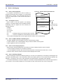
Figure 1-1. External Dimensions
113 mm
Note 1
109 mm
Note 2
68 mm
Note 3
Rear spacer
Front spacer
Note 4
Notes 1 Does not include projection of power switch
2 Includes projection of screw that fixes rear spacer
3 Dimension when rear spacer is made shortest (98 mm when longest)
4 Front spacer can vary from 20 mm (longest) to 5 mm (shortest)
R20UT0450EJ0400 Rev. 4.00
Dec 10, 2012
Page 9 of 57
QB-V850ESJX3H
1.2
CHAPTER 1 GENERAL
System Specifications
This section shows the QB-V850ESJX3H system specifications. For the usage of the debugging function, refer to
ID850QB Ver. 3.40 Operation User’s Manual (U18604E).
Table 1-2. QB-V850ESJX3H System Specifications
Parameter
Specification
Emulation memory
Internal ROM
1 MB max.
capacity
Internal RAM
60 KB max.
External memory
16 MB max. (optional
Program execution
Real-time execution function
Go, Start from Here, Go & Go, Come Here, Restart, Return Out
functions
Non-real-time execution function
Step In, Next Over, Slowmotion
Break functions
Hardware break
Execution: 10 points
Note
) (mapping possible in 1 MB units)
Access: 6 points
Trace functions
Software break
2000 points
Fail-safe break
Non-map, I/O illegal, write protect
Other
Trace full break, forced break, timer overflow break
Trace data types
Branch-source PC, branch-destination PC, all PCs, all execution data,
access data, access address, R/W status, time stamp, DMA point
(start/end)
Trace modes
Real-time trace, Complete trace
Trace events
Delay trigger, section, qualify
Memory capacity
256K frames
Real-time RAM monitoring function
256 bytes × 8 points
Time measurement
Measurement clock
50 MHz
functions
Measurement objects
Beginning through end of program execution
Start event through end event (7 sections)
Maximum measurement time
Approximately 195 hours (When using measurement-dedicated clock
divided by 32)
Minimum resolution
20 ns
Number of timers for measurement
8
Measurement results
Execution time (Start through end of execution)
Maximum, minimum, average, pass count (between events)
Other
Timer overflow break function (1 point)
Time Machine function (optional
Coverage function (optional
Note
Note
)
)
Measured range
Other functions
Contact a GHS tool dealer.
Detection of execution or pass (optional)
Internal ROM space + arbitrary 1 MB space
Mapping function, event function, register manipulation function, memory
manipulation function
Note
Refer to CHAPTER 5 OPTIONAL FUNCTIONS.
Caution
Depending on the debugger, some functions are not supported.
R20UT0450EJ0400 Rev. 4.00
Dec 10, 2012
Page 10 of 57
QB-V850ESJX3H
1.3
CHAPTER 1 GENERAL
Functional Overview
IECUBE is provided with a wealth of debug functions to enable efficient program debugging, in addition to being used
to emulate the operation of a target device. An overview of the functions is provided in this section.
Some functions are not supported, depending on the debugger to be used. See also the manual of the debugger to be
used to confirm.
1.3.1
Program execution function (real-time execution function)
The program execution function enables program execution equivalent to that of the target device. The executed
program can be stopped under various conditions by using the break functions (1.3.3
Break functions (program
execution stop)). The operation of only a function can be checked by executing a program, because a program can be
executed from any address.
1.3.2
Step execution function (non-real-time execution function)
The step execution function can be used to execute instructions one by one, in assemble instruction units. Only
instructions to be executed purely in steps can be executed, because interrupts are not acknowledged during step
execution.
Caution
Step execution to be performed at the C language level is performed by a debugger using the break
function. In this case, interrupts are acknowledged in step execution. Consequently, if processing at
the interrupt destination cannot be completed, step execution may not be completed. For handling
such a case, see the manual of the debugger.
1.3.3
Break functions (program execution stop)
The break functions are used to stop program execution. With IECUBE, program execution can be stopped under the
following various conditions. See (1) to (5) for an overview of each break function.
• An address has been executed
→ Hardware break function, software break function
• A variable has been accessed
→ Hardware break function
• An access-prohibited space has been accessed → Fail-safe break function
• A specific time has elapsed
→ Timer overflow break function
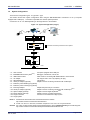
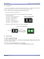
Figure 1-2. Image of Having Set Break Function by Using Debugger ID850QB
Variable values can be checked during a break and a program can be executed again by changing register values,
because the CPU operates even during a break (while the program is stopped). Interrupts generated during the break are
suspended, because basically peripheral functions also operate during the break. Use the peripheral break function (1.3.9
Peripheral break function) to stop peripheral functions during the break.
R20UT0450EJ0400 Rev. 4.00
Dec 10, 2012
Page 11 of 57
QB-V850ESJX3H
CHAPTER 1 GENERAL
(1) Hardware break function
The hardware break function is used to observe the CPU bus cycles and set a break for a specific fetch or access
operation. For example, a break can be set by detecting a state where an address has been executed or a
variable has been accessed. For states that can be set, see 1.3.7
Event function (specific CPU
operation detection).
Caution
The address for which a break has been set is at a position ahead of the address where an actual
access has occurred, because the break set for the access (write, read) is detected at an MEM stage
or a WB stage on the CPU pipeline.
(2) Software break function
The software break function is used to set a break when a specific address has been executed (fetched).
The feature of the software break function is the large number of break points that can be set, because the function
is performed by replacing with a break instruction (DBTRAP instruction) the instruction of an address for which a
break is to be set.
Caution
When obtaining the checksum of a memory space, the actual theoretical value will be different from
the result due to the replacement of the instruction. Furthermore, break points cannot be set for a
ROM that has been connected to an external bus. Use the hardware break function to solve such
problems.
(3) Fail-safe break function
This function is used to set a break when the CPU has performed an illegal operation. For example, a break is set
when a peripheral I/O register, that has written to a ROM area and is to be accessed in 8-bit units, is accessed in
16-bit units. The following illegal operations can be detected by using the fail-safe break function.
{ Accesses (fetching, reading, writing) to areas that are not mapped (prohibited areas)
{ A write operation for the ROM area
{ The following illegal operations for a peripheral I/O register
• Accesses with different access bit widths
• A write operation for a read-only register
• A read operation for a write-only register
(4) Timer overflow break function
This function is used to set a break when a time set by using the time measurement function (1.3.6
Time
measurement function) has elapsed. For example, if the execution time of a function must be 2 ms, a break can
be set when at least 2 ms have elapsed between starting and ending the function. This function and the trace
function (1.3.4
Trace function (program execution history)) can be used together to find the source that
has taken time.
(5) Forcible break function
This function is used to forcibly stop a program when it is desired to be stopped.
R20UT0450EJ0400 Rev. 4.00
Dec 10, 2012
Page 12 of 57
QB-V850ESJX3H
1.3.4
CHAPTER 1 GENERAL
Trace function (program execution history)
The trace function can be used to check the CPU execution history (trace). Items (1) to (9) can be recorded in the
execution history.
Figure 1-3. Image of Execution History (Trace) with Debugger ID850QB
(1) Program counter (PC) of branch source and branch destination
The PCs of a branch source and a branch destination can be recorded in the history.
Consequently, practically all executed programs can be checked, because programs executed between branch
points also will be clarified. The amount of trace memory used can be saved and more history items can be traced
by that amount, by recording only branch information. (The amount of traces that can be traced back depends on
the number of branches.)
(2) All executed addresses
All executed address can be recorded in the history.
Normally, the programs that have been executed can be traced back if branch PC information described in (1) is
available. This trace information is mainly used by the coverage function (5.2 Coverage Measurement Function).
(3) Access data/access address
Access addresses for memories and peripheral I/O registers, and access data can be recorded in the history.
Read and write operations can also be recorded in the history.
Caution
Accesses to CPU program registers (such as r1 and r2) and system registers (such as PSW and
EIPC) cannot be recorded in the history. Furthermore, if an internal RAM is successively accessed
for at least 32 times, some trace information may be omitted. (Whether trace information has been
omitted can be checked in the debugger display.)
To prevent such omissions, IECUBE is provided with a mode (trace priority mode) in which the CPU
execution cycle is stopped and the acquisition of traces is prioritized. Note that, when the trace
priority mode is executed, however, operation may not be performed in real-time.
(4) Access program counter (PC)
PCs that have accessed memories and peripheral I/O registers can be recorded in the history.
R20UT0450EJ0400 Rev. 4.00
Dec 10, 2012
Page 13 of 57
QB-V850ESJX3H
CHAPTER 1 GENERAL
(5) Time stamp
The time elapsed from the trace start point can be added to each trace information. The timer performance for time
stamps is the same as that of the time measurement function (1.3.6
Time measurement function). For the
timer performance, see the time measurement function column in Table 1-2.
QB-V850ESJX3H System
Specifications.
Caution
The addition of a time stamp is not suited for accurately measuring time in 1-instruction units,
because only one time stamp is added to four pieces of trace information at most. If all execution
addresses are left as trace information, only one time stamp is added to four instructions. The same
applies when the timer resolution is slower than the CPU operation frequency.
Use the time
measurement function (1.3.6 Time measurement function) to accurately measure time.
(6) DMA start and end points (DMA points)
When the DMA function of the target microcontroller is being used, the DMA start and end points can be recorded
in the history.
(7) History of specific sections (section trace)
Only specific sections can be recorded in the history by using the event function (1.3.7
Event function
(specific CPU operation detection)) in combination. For example, the execution history of from the start to the
end of a function can be recorded.
(8) History of specific phenomenon occurred (qualify trace)
Only the occurrence of specific phenomena can be recorded in the history by using the event function (1.3.7
Event function (specific CPU operation detection)) in combination.
For example, a history of having accessed to only a variable can be recorded.
(9) Recording histories before and after specific phenomenon has occurred (delay trigger trace)
The history after a specific phenomenon has occurred can be recorded by using the event function (1.3.7
Event function (specific CPU operation detection)) in combination. This is similar to being able to observe a
signal waveform by assuming an edge as a trigger, when using an oscilloscope to observe a signal.
For example, the program execution histories before and after a write access has been performed for a variable
can be viewed.
R20UT0450EJ0400 Rev. 4.00
Dec 10, 2012
Page 14 of 57
QB-V850ESJX3H
1.3.5
CHAPTER 1 GENERAL
Real-time RAM monitoring function (checking RAM values during program execution)
The real-time RAM monitoring function can be used to check RAM values during program execution.
Real-time
operation is guaranteed so that program execution is not affected when reading RAM values. Furthermore, whether the
RAM has been read or written can be checked.
Figure 1-4. Image of Having Displayed Memory Space by Using Debugger ID850QB
Write
Read
Write & Read
Caution
When a RAM to be monitored has been changed during a break or changed by the DMA function of
the target microcontroller, the changed values cannot be monitored. Only RAM values that have
been changed by CPU accesses can be monitored during program execution.
1.3.6
Time measurement function
This function is used to measure the execution time of a specific section. The measurement start and end points can
be set by using the event function (1.3.7
Event function (specific CPU operation detection)).
In addition, the maximum, minimum, and average execution time and the number by which the measurement section
has been passed can be measured. For the performance of the time measurement function, see Table 1-2.
QB-
V850ESJX3H System Specifications.
Figure 1-5. Image of Having Displayed Time Measurement Result by Using Debugger ID850QB
R20UT0450EJ0400 Rev. 4.00
Dec 10, 2012
Page 15 of 57
QB-V850ESJX3H
1.3.7
CHAPTER 1 GENERAL
Event function (specific CPU operation detection)
The event function is used to detect specific fetch and access operations by observing the CPU bus cycle. CPU
operations, such as of an address being executed and a variable being accessed can be detected. Such specific CPU
operations are called events. Use the event function together with the following functions.
• Hardware break function
• Trace function
• Time measurement function
The events that can be registered by using the event function are as follows.
(1) Pre-execution event
A pre-execution event is detected when execution of an address is attempted. It can be used only with the
hardware break function. Two pre-execution event points can be specified.
[Detection conditions that can be specified]
- Execution address
(2) Post-execution event
A post-execution event is detected when an address has been executed. The address of a post-execution event
can be specified as a range. Up to eight post-execution event points can be specified, but if the execution address
has been specified as a range, two points will be consumed. When the execution address has been specified as a
range for all events, four event points can be specified.
[Detection conditions that can be specified]
- Execution address (can be specified as a range)
(3) Access event
An access event is detected when an address has been accessed (read or written). The following detection
conditions can be specified for an access event.
Up to six access event points can be specified, but if the access address has been specified as a range, two points
will be consumed. When the access address has been specified as a range for all events, three event points can
be specified.
[Detection conditions that can be specified]
- Access address (can be specified as a range)
- Access data
- Access size
- Access status (read, write, both read and write)
1.3.8
Event link function (event combinations)
The event link function is used to combine into one event, events that have been registered by using the event function
(1.3.7
Event function (specific CPU operation detection)). It is used to detect a specific sequence, such as when an
address has been executed after a variable was accessed.
1.3.9
Peripheral break function
When the break function has been used to stop program execution, peripheral functions other than the watchdog timer
continue to operate in general, but some peripheral functions can be stopped by using the peripheral break function. See
4.2.7 Operation during Break for details.
R20UT0450EJ0400 Rev. 4.00
Dec 10, 2012
Page 16 of 57
QB-V850ESJX3H
CHAPTER 1 GENERAL
1.3.10 Mask function
The mask function can be used to mask the following sources.
• Reset (external reset)
• Non-maskable interrupt
• Bus hold request input (¯¯¯¯¯¯¯¯¯¯¯
HLDRQ
pin)
¯¯¯¯¯¯¯¯
• External wait input ( WAIT pin)
1.3.11 Optional functions
The following optional functions can be added to IECUBE. See CHAPTER 5 OPTIONAL FUNCTIONS for details.
• Memory emulation function
• Coverage function
• TimeMachineTM function
1.3.12 Function to control reset when power of target system is turned off
When the power supply voltage of the target interface is decreased by 10% from the value stated in Table 1-1 when the
target system is connected and a program is being executed, a state equivalent to a reset state of the target device is
entered. When the power supply voltage of the target interface has been restored, the reset will be released and program
execution will be started.
Consequently, the operation of the target system when its power is turned on can be pseudo-checked.
Caution
The operation performed after a reset by this function will not be completely equivalent to an
operation of the target device. Mount an actual device and perform final verification of the operation
when starting the power supply.
R20UT0450EJ0400 Rev. 4.00
Dec 10, 2012
Page 17 of 57
QB-V850ESJX3H
1.4
CHAPTER 1 GENERAL
System Configuration
There are two configuration types: S Type and T Type.
This section shows each system configuration when using the QB-V850ESJX3H connected to a PC (a computer
equipped with a USB port). Connection is possible even without optional products.
Connectors <9> to <13> differ depending on the target device to be emulated.
Figure 1-6. System Configuration (S Type)
<5>
<1>
<3>
<4>
<2>
<6>
<7>
: Products enclosed by broken lines are optional.
<8>
<9>
<10>
<12>
<11>
<13>
<1>
<2>
<3>
<4>
<5>
<6>
<7>
<8>
<9>
<10>
<11>
<12>
<13>
<14>
<14>
Host machine:
Computer equipped with a USB port
ID850QB Disk/Accessory DiskNote 1:
Debugger, USB drivers, manual, etc.
USB interface cable:
Cable used for connecting QB-V850ESJX3H to host machine
AC adapter:
Can support 100 to 240 V by replacing AC plug
QB-V850ESJX3H:
This product
Check pin adapter (optional):
Adapter used for monitoring waveforms with oscilloscope
Extension probe flexible type (optional)
Extension probe coaxial type (optional)
Exchange adapter:
Adapter that performs pin conversion
Note 2
Check pin adapter (optional):
Adapter used for monitoring waveforms with oscilloscope
Note 2
Space adapter (optional):
Adapter used for height adjustment
Mount adapter (optional):
Adapter used for mounting target device
Target connector:
Connector to be soldered to target system
Target system
Notes 1. Download the device file from the Renesas Electronics website.
http://www2.renesas.com/micro/en/ods/index.html
2. If both <10> and <11> are used, connection sequence of <10> and <11> may be reversed.
Remark For notes on target system design and package drawings, refer to [Related Content] on the following URL.
http://www2.renesas.com/micro/en/development/asia/Emulator/IE/iecube.html
R20UT0450EJ0400 Rev. 4.00
Dec 10, 2012
Page 18 of 57
QB-V850ESJX3H
CHAPTER 1 GENERAL
Figure 1-7. System Configuration (T Type)
<5>
<1>
<3>
<4>
<2>
<6>
<7>
: Products enclosed by broken lines are optional.
<8>
<9>
<10>
<11>
<12>
<13>
<14>
<1> Host machine:
Computer equipped with a USB port
<2> ID850QB Disk/Accessory DiskNote:
Debugger, USB drivers, manual, etc.
<3> USB interface cable:
Cable used for connecting QB-V850ESJX3H to host machine
<4> AC adapter:
Can support 100 to 240 V by replacing AC plug
<5> QB-V850ESJX3H:
This product
<6> Check pin adapter (optional):
Adapter used for monitoring waveforms with oscilloscope
<7> Extension probe flexible type (optional)
<8> Extension probe coaxial type (optional)
<9> Exchange adapter:
Adapter that performs pin conversion
<10> Space adapter (optional):
Adapter used for height adjustment
<11> Mount adapter (optional):
Adapter used for mounting target device
<12> YQ connector:
Connector used for connecting emulator
<13> Target connector:
Connector to be soldered to target system
<14> Target system
Note
Download the device file from the Renesas Electronics website.
Remark
http://www2.renesas.com/micro/en/ods/index.html
For notes on target system design and package drawings, refer to [Related Content] on the following URL.
http://www2.renesas.com/micro/en/development/asia/Emulator/IE/iecube.html
R20UT0450EJ0400 Rev. 4.00
Dec 10, 2012
Page 19 of 57
QB-V850ESJX3H
CHAPTER 1 GENERAL
Table 1-3. List of Probe/Connector for Each Target Device (S Type)
No.
Name
Target Device to Be Emulated
V850ES/JC3-H V850ES/JC3-H V850ES/JC3-H V850ES/JE3-H V850ES/JG3-U V850ES/JG3-H V850ES/JH3-U,
(40-Pin K8)
(48-Pin GA)
(48-Pin K8)
(64-Pin GB)
(100-Pin GC)
(100-Pin GC)
V850ES/JH3-H,
V850ES/ST3
(128-Pin GF)
<6> Check pin adapter QB-144-CA-01 (sold separately)
<7> Extension probe
QB-144-EP-02S (sold separately)
(flexible type)
<8> Extension probe
QB-144-EP-01S (sold separately)
(coaxial type)
<9> Exchange
adapter
QB-40K8-EA- QB-48GA-
QB-48K8-EA- QB-64GB-
01S
01S
EA-01S
EA-02S
QB-100GC-
QB-100GC-
QB-128GF-
EA-04S
EA-05S
EA-01S
(sold
separately)
<10> Check pin adapter
-
(sold
Note
separately)
(sold
Note
separately)
Note
QB-64-CA-
QB-100-CA-01S
QB-128-CA-
01S
(sold separately)
01S
(sold
separately)
<11> Space adapter
-
QB-64-SA-
QB-100-SA-01S
QB-144-SA-
01S
(sold separately)
01S
(sold
separately)
<12> Mount adapter
-
QB-64GB-
QB-100GC-MA-01S
QB-128GF-
MA-01S
(sold separately)
MA-01S
(sold
separately)
<13> Target connector QB-40K8-TC- QB-48GA-TC- QB-48K8-TC- QB-64GB-TC- QB-100GC-TC-01S
01S
01S
01S
01S
(sold separately)
Note
QB-128GFTC-01S
(sold
separately)
R20UT0450EJ0400 Rev. 4.00
Dec 10, 2012
Note
Page 20 of 57
QB-V850ESJX3H
CHAPTER 1 GENERAL
Table 1-4. List of Probe/Connector for Each Target Device (T Type)
No.
Name
Target Device to Be Emulated
V850ES/JG3-U
V850ES/JG3-H
V850ES/JH3-U,
(100-Pin GC)
(100-Pin GC)
V850ES/JH3-H,
V850ES/ST3
(128-Pin GF)
<6>
Check pin adapter
QB-144-CA-01 (sold separately)
<7>
Extension probe (coaxial type)
QB-144-EP-01S (sold separately)
<8>
Extension probe (flexible type)
QB-144-EP-02S (sold separately)
<9>
Exchange adapter
QB-100GC-EA-05T
(sold separately)
<10> Space adapter
Note
QB-100GC-EA-06T
(sold separately)
Note
QB-128GF-EA-02T
(sold separately)
Note
QB-128GF-YS-01T
QB-100GC-YS-01T (sold separately)
(sold separately)
<11> Mount adapter
QB-128GF-HQ-01T
QB-100GC-HQ-01T (sold separately)
(sold separately)
<12> YQ connector
QB-100GC-YQ-01T (sold separately)
Note
QB-128GF-YQ-01T
(sold separately)
<13> Target connector
QB-100GC-NQ-01T (sold separately)
Note
Note
QB-128GF-NQ-01T
(sold separately)
Note
Note These accessories are supplied depending on the part number ordered (Refer to 1.5 Package Contents).
R20UT0450EJ0400 Rev. 4.00
Dec 10, 2012
Page 21 of 57
QB-V850ESJX3H
1.5
CHAPTER 1 GENERAL
Package Contents
The following items have been placed in the QB-V850ESJX3H packing box. Please check the contents.
Products supplied with QB-V850ESJX3H-ZZZ
1:
QB-V850ESJX3H
2:
AC adapter
3:
USB interface cable
4:
ID850QB Disk (CD-ROM)
5:
Accessory Disk (CD-ROM)
6:
IECUBE Setup Manual (J/E)
7:
User registration (Guarantee card and software contract in one)
8:
Simple flash memory programmer QB-MINI2
9:
Probe holder
10:
Parts board (for clock)
Products supplied with QB-V850ESJX3H-S40K8
1 to 10
11: Exchange adapter
QB-40K8-EA-01S
12: Target connector
QB-40K8-TC-01S
Products supplied with QB-V850ESJX3H-S48GA
1 to 10
11: Exchange adapter
QB-48GA-EA-01S
12: Target connector
QB-48GA-TC-01S
Products supplied with QB-V850ESJX3H-S48K8
1 to 10
11: Exchange adapter
QB-48K8-EA-01S
12: Target connector
QB-48K8-TC-01S
Products supplied with QB-V850ESJX3H-S64GB
1 to 10
11: Exchange adapter
QB-64GB-EA-02S
12: Target connector
QB-64GB-TC-01S
Products supplied with QB-V850ESJX3H-S100GC
1 to 10
11:
Exchange adapter (2 xxxxx)
12:
Target connector
QB-100GC-EA-04S (V850ES/JG3-U)
QB-100GC-EA-05S (V850ES/JG3-H)
QB-100GC-TC-01S
Products supplied with QB-V850ESJX3H-T100GC
1 to 10
11:
Exchange adapter (2 xxxxx)
QB-100GC-EA-05T (V850ES/JG3-U)
12:
YQ connector
QB-100GC-YQ-01T
13:
Target connector
QB-100GC-NQ-01T
QB-100GC-EA-06T (V850ES/JG3-H)
R20UT0450EJ0400 Rev. 4.00
Dec 10, 2012
Page 22 of 57
QB-V850ESJX3H
CHAPTER 1 GENERAL
Products supplied with QB-V850ESJX3H-S128GF
1 to 10
11:
Exchange adapter
QB-128GF-EA-01S
12:
YQ connector
QB-128GF-TC-01S
Products supplied with QB-V850ESJX3H-T128GF
1 to 10
11:
Exchange adapter
QB-128GF-EA-02T
12:
YQ connector
QB-128GF-YQ-01T
13:
Target connector
QB-128GF-NQ-01T
R20UT0450EJ0400 Rev. 4.00
Dec 10, 2012
Page 23 of 57
QB-V850ESJX3H
CHAPTER 2 SETUP PROCEDURE
CHAPTER 2 SETUP PROCEDURE
This chapter explains the QB-V850ESJX3H setup procedure.
Setup can be completed by performing installation/setup in the order in which it appears in this chapter.
Perform setup along the lines of the following procedure.
Main clock settings
A 6 MHz resonator will be mounted upon shipment.
If 6 MHz is acceptable for the frequency of the resonator, the setting is not required to be changed.
If modification is necessary, see 2.2 Removal of Acrylic Board and 2.3 Clock Settings.
Software settings
See 2.4 Software Settings.
Mounting and connecting connectors
When using the S Type, see 2.5 Mounting and Connecting Connectors (When Using S Type).
When using the T Type, see 2.6 Mounting and Connecting Connectors (When Using T Type).
Connecting QB-V850ESJX3H to target system
See 2.7 Connecting QB-V850ESJX3H to Target System.
• When not using the extension probe (QB-144-EP-01S/02S): see 2.7.1.
• When using the extension probe (QB-144-EP-01S/02S): see 2.7.2.
Connecting USB interface cable and AC adapter
See 2.8 Connecting USB Interface Cable and AC Adapter.
Switching power on and off
See 2.9 Switching Power On and Off
R20UT0450EJ0400 Rev. 4.00
Dec 10, 2012
Page 24 of 57
QB-V850ESJX3H
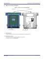
2.1
CHAPTER 2 SETUP PROCEDURE
Names and Functions of Hardware
Figure 2-1. Names of Parts of QB-V850ESJX3H
Top View
Bottom View
Power switch
OSC1
1pin
Connector for
parts board
POWER TARGET
CN3
CN2
CN1
(1) CN1, CN2, CN3
These connectors are used to connect the exchange adapter or extension probe.
(2) Parts board connector
This connector is used to mount an oscillator for the main clock.
(For details, refer to 2.3 Clock Settings.)
R20UT0450EJ0400 Rev. 4.00
Dec 10, 2012
Page 25 of 57
QB-V850ESJX3H
CHAPTER 2 SETUP PROCEDURE
(3) POWER (Red LED)
This is an LED that shows whether or not the power supply of the QB-V850ESJX3H is switched on.
LED State
QB-V850ESJX3H State
Lit
Power switch ON
Not lit
Power switch OFF or AC adapter not connected to QB-V850ESJX3H
Blinking
Internal error occurred (Contact an NEC Electronics sales representative or distributor)
(4) TARGET (Green LED)
This is an LED that shows whether or not the power supply of the target system is switched on.
LED State
Target System State
Lit
Target system power supply ON
Not lit
Target system power supply OFF or target system not connected
(5) Power switch
This is the power switch of the QB-V850ESJX3H.
It is OFF at shipment.
2.2
Removal of Acrylic Board
To change the jumper or clock setting, the acrylic board on the bottom of the QB-V850ESJX3H must be removed.
The acrylic board can be removed by lifting it up.
Figure 2-2. Acrylic Board Removal Method
R20UT0450EJ0400 Rev. 4.00
Dec 10, 2012
Page 26 of 57
QB-V850ESJX3H
2.3
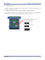
CHAPTER 2 SETUP PROCEDURE
Clock Settings
The main clock is generated from the oscillator mounted in the QB-V850ESJX3H. It oscillates at 6 MHz with the factory
setting. To change the oscillation clock frequency, perform settings with the following procedures.
Caution
This product does not support clock input from the target system.
(1) Removing parts board on MAIN CLOCK socket
(2) Solder a resonator and a capacitor to the parts board supplied with the QB-V850ESJX3H.
The setting is as follows.
Figure 2-3. Setting Parts Board
Pins 1 and 14: Be sure to short these pins.
Pins 2 and 13: Connect a capacitor.
7
6
5
4 3
2 1
8
9 10 11 12 13 14
Pins 3 and 12: Connect a resonator.
Pins 4 and 11: Leave open.
Pins 5 and 10: Connect a capacitor.
Pins 6 and 9:
Be sure to short these pins.
Pins 7 and 8:
Be sure to leave open.
(3) Insert the parts board into MAIN CLOCK socket of the QB-V850ESJX3H.
Figure 2-4. Inserting Parts Board
7
6
5
4 3
2 1
Insert
Parts board
8
9 10 11 12 13 14
QB-V850ESJX3H board
2.4
2.4.1
Software Settings
When using ID850QB as debugger
Be sure to use ID850QB of V3.50 or later.
For details of setting up ID850QB, refer to the V850 Series Integrated Debugger ID850QB Operating Precautions
supplied with the debugger (ID850QB).
2.4.2
When using other than ID850QB (MULTITM, etc.) as debugger
Refer to the user’s manual of the debugger used and the V850 IECUBE Setup Manual (supplied).
R20UT0450EJ0400 Rev. 4.00
Dec 10, 2012
Page 27 of 57
QB-V850ESJX3H
2.5
CHAPTER 2 SETUP PROCEDURE
Mounting and Connecting Connectors (When Using S Type)
This section describes the methods for connecting the QB-V850ESJX3H to the target system when using the S Type.
Make connections with both the QB-V850ESJX3H and target system powered off.
The following abbreviations are used in this section.
• TC: Target connector
• EA: Exchange adapter
• MA: Mount adapter
• CA: Check pin adapter
• SA: Space adapter
2.5.1
Mounting TC to target system
(1) Apply cream solder to the foot pattern of the target system for mounting an IC.
(2) A circular projection is at the center of the bottom side of the TC (refer to Figure 2-5). Sparingly apply two-liquid
hardening epoxy adhesive (type that hardens in 15 to 30 minutes is recommended) to temporarily secure the
connector at the specified position on the target system. At this time, match the position of pin 1 (position where a
corner is cut) with the position of pin 1 from the target system.
(3) Soldering condition of TC
Figure 2-5. TC Projection
(a) Reflow soldering
At 245°C for a maximum of 20 seconds (main heating)
(b) Manual soldering
At 330°C for a maximum of 3 seconds (per pin)
(4) Precautions on flux splatter
If the solder flux splatters when the connector is soldered, faulty
contact may occur. Be sure to cover the upper part of the connector with aluminum foil. Do not clean the
connector because the flux solvent may remain inside the connector.
2.5.2
Inserting EA into TC
Match the pin 1 position of the EA, MA, CA, or SA to the pin 1 position of the TC and insert it (corner cuts match in
both).
(a) When inserting or removing, hold down the TC with your fingers so that there is no force on the TC.
(b) When inserting or removing, be careful of the direction of wiggling (refer to Figure 2-6).
As a tool when removing, insert some kind of thin non-conductive material such as a wooden stick in between the
TC and EA and wiggle it in the direction shown in Figure 2-6 while slowly removing. Be careful since the connector
will be damaged if this is done in the wrong direction.
Figure 2-6. Inserting and Removing
SA
TC
R20UT0450EJ0400 Rev. 4.00
Dec 10, 2012
Page 28 of 57
QB-V850ESJX3H
2.5.3
CHAPTER 2 SETUP PROCEDURE
Precautions for handling TC, EA, MA, CA, and SA
(1) Cause of faulty contact of connector
(a) If flux gets inside the connector when the TC is soldered
It is easy for flux to get inside of the connector. Clean the connector several times with a solvent such as
alcohol if flux gets inside.
If conduction is still unstable, repeat cleaning.
(b) If dust gets inside the connector
Faulty contact occurs if dust such as a thread gets inside the connector. Remove dust with a brush.
(c) Cautions on using the CA or SA
When the CA or SA is used, a fractional delay time of signal propagation and a little capacitance are
generated as a result of inserting the adapter. Make a thorough evaluation by connecting the target system.
(2) Cautions on inserting and removing the connector
(a) When inserting or removing the connector, be sure to hold down the lower (mating) connector or board with
your fingers.
(b) Before inserting a connector, make sure that the connectors are correctly positioned.
If the connector is inserted incorrectly positioned, it may be damaged.
(c) When removing a connector, insert some kind of thin non-conductive material such as a wooden stick beneath
the connector to protect the board from being damaged. Do not remove the connector all at once. Remove it
slowly.
If only a metallic object such as a screwdriver is available, wind a soft cloth around its tip.
(3) Check pin adapter QB-144-CA-01
The check pin adapter QB-144-CA-01 is an optional product for IECUBE, and can be used to measure the
waveform between IECUBE and the target system.
Since the pins on the QB-144-CA-01 do not correspond to the pin layout in each device, the pin header cover must
be mounted according to the device to be used.
For mounting methods of the pin header cover, refer to [Related Content] on the following webpage.
http://www2.renesas.com/micro/en/development/asia/Emulator/IE/iecube.html
(4) Check pin adapter (QB-xxx-CA-01S)
When using a check pin adapter (QB-xxx-CA-01S), connect a extension probe (QB-144-EP-01S/02S) (sold
separately).
R20UT0450EJ0400 Rev. 4.00
Dec 10, 2012
Page 29 of 57
QB-V850ESJX3H
2.5.4
CHAPTER 2 SETUP PROCEDURE
Precautions for mounting IC using MA
(1) Confirm that there is no weld flash in the resin (sealant part) of the IC. If there is weld flash, remove it using a knife
or the like.
(2) Confirm that there is no weld flash breaking or bending of IC leads. In particular, confirm the planarity of IC leads.
If there is abnormality in the planarity, correct that portion.
(3) Viewing the contact pins on the bottom of the MA (IC mounting part) from the top, if there are foreign bodies on
them, remove them using a brush or the like.
After confirming (1) to (3), fit the IC to the bottom of the MA. Also fit the top (cover) of the MA.
(4) Put the supplied M2 × 6 mm screws in the four accessory holes on the top (cover) of the MA and fasten the screws
in opposite corners. At that time, use either the dedicated screwdriver that is supplied or a torque driver to fasten
them equally in turn with a tightening torque of 0.054 Nm (MAX.). Since the contact is poor if tightening is too great,
once you have lightly fastened the screws on the top of the MA, tighten them again.
(5) Depending on the use environment, when starting up a device that has been left for a long time, starting it may be
difficult. In this case, loosen the screws slightly and then retighten them.
(6) If startup still is difficult after (5) above, check (1) to (3) again.
(7) Tightening the screws on the top of the MA too much may give rise to cracks in the molded part of the MA (plastic
part) and bend the mold into a bowed shape, making contact poor.
(8) After soldering the MA, do not perform cleaning by flux immersion or vapor.
R20UT0450EJ0400 Rev. 4.00
Dec 10, 2012
Page 30 of 57
QB-V850ESJX3H
2.6
CHAPTER 2 SETUP PROCEDURE
Mounting and Connecting Connectors (When Using T Type)
This section describes the methods for connecting the QB-V850ESJX3H to the target system when using the T Type.
Make connections with both the QB-V850ESJX3H and target system powered off.
The following abbreviations are used in this section.
• TC: Target connector
• YQ: YQ connector
• EA: Exchange adapter
• MA: Mount adapter
• CA: Check pin adapter
• SA: Space adapter
2.6.1
Mounting TC in target system
(1) Thinly apply a two-component epoxy adhesive (hardening time at least 30 minutes) to the ends of the four
projections on the base of the TC and adhere the TC to the user board (clean the surface of the user board using
alcohol or the like). If alignment of user board pads to TC leads is difficult, align them as in (2).
(2) Align by inserting the guide pins for alignment for the TC (NQGUIDE) through the pin holes on the top of the TC.
Accessory holes are φ1.0 mm non-through holes in two or three places.
(For hole positions, see the particular TC drawing.)
(3) Solder after fitting the MA to the TC. This is to prevent troubles such as flux or solder splatter and adhering to the
TC contact pins when soldering.
● Soldering conditions
Caution
Solder reflow
At 260°C for a maximum of 10 seconds
Manual soldering
At 350°C for a maximum of 5 seconds (per pin)
Do not perform cleaning by flux immersion or vapor.
(4) Remove the guide pins.
2.6.2
Connecting YQ on TC
(1) After confirming that there are no broken or bent YQ contact pins, fit the YQ in the TC and fasten it using the
supplied YQGUIDE (for the fastening method, see the next step, (2)). If repeatedly inserting and removing, be
sure to inspect the YQ pins before fitting. If pins are bent, correct them using something thin and flat such as
the edge of a knife.
R20UT0450EJ0400 Rev. 4.00
Dec 10, 2012
Page 31 of 57
QB-V850ESJX3H
CHAPTER 2 SETUP PROCEDURE
(2) Fasten YQ to the TC on the target system using the supplied YQGUIDE. Fasten the screws equally in the four
corners using the supplied flat-blade screwdriver or a torque driver. The tightening torque of YQGUIDE is 0.054
Nm (MAX.). Too great tightening causes bad connections.
Four screws for fitting to the MA (M2 x 10 mm / 4 units) are included with YQ.
EA
YQGUIDE supplied with YQ
YQ
TC
Target system
2.6.3
Inserting EA into YQ
Match the pin 1 position of the YQ or SA (corner cuts match in both) to the pin 1 position of the EA and insert it.
• When inserting or removing, press on the TC, YQ, and SA with a finger so that there is no force on the TC.
• When inserting or removing, be careful of the direction of wiggling.
As a tool when removing, insert some kind of thin non-conductive material such as a wooden stick between the YQ
(SA) and EA and wiggle it while slowly removing. Be careful since the connector will be damaged if this is done in the
wrong direction.
2.6.4
Precautions for handling TC, YQ, and SA
(1) When taking the TC from the box, press down on the body and take out the sponge first.
(2) Since the pins of the YQ are thin and easily bent, be careful. When inserting it in the TC, confirm that there are no
bent pins.
(3) When screwing a YQ soldered to a board to the TC, fasten the screws in four places in turn using a #0 or #1
Phillips precision screwdriver or torque driver after tentatively tightening them. Fix the torque at 0.054 Nm (MAX.).
If just one place is overtightened, it may cause poor contact. Moreover, a board being connected to the YQ must
have accessory holes in prescribed positions (4 places: φ2.3 mm or φ3.3 mm). The φ3.8 mm or φ4.3 mm that is the
screw head size is an area where wiring is prohibited.
(4) In YQ and SA removal, since there is a danger of YQ pins being bent or broken when prying and wiggling, remove
them gradually using a flatbladed screwdriver from four directions. Moreover, to connect and use the YQ and SA,
screw the YQ to the TC according to the YQGUIDE (included with the YQ) using a 2.3 mm flatbladed screwdriver
and then connect it to the SA. Fix the torque at 0.054 Nm (MAX.). If even one place is overtightened, it may cause
poor contact..
(5) For the TC, YQ, and SA, since there is a danger that cleaning fluid on the structure will remain in the connector, do
not perform cleaning.
(6) TC, IC, and YQ cannot be used in combination.
(7) An TC/YQ system cannot be used in an environment of vibrations or shocks.
R20UT0450EJ0400 Rev. 4.00
Dec 10, 2012
Page 32 of 57
QB-V850ESJX3H
CHAPTER 2 SETUP PROCEDURE
(8) It is assumed that this product will be used in system development and evaluation. Moreover, when used in Japan,
Electrical Appliance and Material Control Law and electromagnetic disturbance countermeasures have not been
applied.
(9) Since there are rare cases of shape change if the box is left for a long time in a place where it is 50°C or higher, for
safekeeping, store it in a place where it is no higher than 40°C and direct sunlight does not hit it.
(10) For details about handling the TC, YQ, and SA, see the NQPACK series technical materials at the website of Tokyo
Eletech Corporation.
Tokyo Eletech Corporation website: http://www.tetc.co.jp/
(11) The check pin adapter QB-144-CA-01 is an optional product for IECUBE, and can be used to measure the
waveform between IECUBE and the target system.
Since the pins on the QB-144-CA-01 do not correspond to the pin layout in each device, the pin header cover must
be mounted according to the device to be used.
For mounting methods of the pin header cover, refer to [Related Content] on the following webpage.
http://www2.renesas.com/micro/en/development/asia/Emulator/IE/iecube.html
2.6.5
Precautions for mounting IC using TC and MA
(1) Confirm that there is no weld flash in the resin (sealant part) of the IC. If there is weld flash, remove it using a knife
or the like.
(2) Confirm that there is no weld flash breaking or bending of IC leads. In particular, confirm the planarity of IC leads.
If there is abnormality in the planarity, correct that portion.
(3) Viewing the TC contact pins from the top, if there are foreign bodies on them, remove them using a brush or the
like.
After confirming (1) to (3), fit the IC to the TC. Also fit the MA.
(4) Put the supplied M2 × 6 mm screws in the four accessory holes of the MA and fasten the screws in opposite
corners. At that time, use either the dedicated screwdriver that is supplied or a torque driver to fasten them equally
in turn with a tightening torque of 0.054 Nm (MAX.). Since the contact is poor if tightening is too great, once you
have lightly fastened the MA screws, tighten them again.
(5) Depending on the use environment, when starting up a device that has been left for a long time, starting it may be
difficult. In this case, loosen the screws slightly and then retighten them.
(6) If startup still is difficult after (5) above, check (1) to (3) again.
(7) Tightening the screws of the MA too much may give rise to cracks in the molded part of the MA (plastic part) and
bend the mold into a bowed shape, making contact poor.
(8) After soldering the TC, do not perform cleaning by flux immersion or vapor.
R20UT0450EJ0400 Rev. 4.00
Dec 10, 2012
Page 33 of 57
QB-V850ESJX3H
2.7
2.7.1
CHAPTER 2 SETUP PROCEDURE
Connecting QB-V850ESJX3H to Target System
When not using extension probe (QB-144-EP-01S/02S)
The QB-V850ESJX3H can be connected to the target system without using an extension probe.
Adjust the height by using the spacer at the rear part of the QB-V850ESJX3H, so that no stress is applied to the
exchange adapter, the target connector, and other connectors.
Sufficiently insulate the target system.
Figure 2-7. Connection Without Extension Probe
QB-V850ESJX3H
Height adjustable
Exchange adapter
Rear spacer
Target connector
Remark
The connector shown in the above figure is the connector used with the S Type. When used with the T Type,
read this connector as that of the T Type.
R20UT0450EJ0400 Rev. 4.00
Dec 10, 2012
Page 34 of 57
QB-V850ESJX3H
2.7.2
CHAPTER 2 SETUP PROCEDURE
When using extension probe (QB-144-EP-01S/02S)
When using the extension probe (QB-144-EP-01S/02S), connect the QB-V850ESJX3H to the target system using the
following procedure.
(a) Connecting probe holder
Use the probe holder (supplied with the QB-V850ESJX3H) to connect the extension probe to the QB-V850ESJX3H,
as shown below.
Figure 2-8. Using Probe Holder
<1> Connect the QB-V850ESJX3H to the probe.
Extension probe holder
Probe holder
Insert
QB-V850ESJX3H
<2> Insert the probe holder into the QB-V850ESJX3H.
Insert the probe holder into the QB-V850ESJX3H until
you hear a click (note the direction).
(b) Connection of extension probe GND wire
There are three GND wires in the extension probe. Connect them to the QB-V850ESJX3H and target system.
<1> Fasten the GND wire on the QB-V850ESJX3H side of the extension probe to the nut on the bottom of the
QB-V850ESJX3H using a #0 or #1 Phillips precision screwdriver (connection of B to A in Figure 2-9).
<2> Next insert the connector on the top of the extension probe into the connector at the opening on the bottom of
the QB-V850ESJX3H from below being careful of the insertion direction (connection of C in Figure 2-9 to
QB-V850ESJX3H).
R20UT0450EJ0400 Rev. 4.00
Dec 10, 2012
Page 35 of 57
QB-V850ESJX3H
CHAPTER 2 SETUP PROCEDURE
Figure 2-9. GND Wire
QB-V850ESJX3H
Target system
Remark
The connector shown in the above figure is the connector used with the S Type. When used with the T Type,
read this connector as that of the T Type.
<3> Connect two GND wires on the target system side of the extension probe to the target system GND.
<4> If a pin or screw is fastened to the target system GND, remove the transparent terminal cover on the end of
the GND wire and fasten the Y type pin of the GND wire to the target system (G in Figure 2-9). If the GND
on the target system is an exposed pad, likewise fasten the Y type pin to the pad on the target system by
soldering (H in Figure 2-9) (recommended soldering iron temperature setting: 300°C).
<5> If the target system has only one GND, connect only one of the GND wires of the extension probe. Cut off
the other GND wires with a nipper or leave it as is without removing the pin cover.
R20UT0450EJ0400 Rev. 4.00
Dec 10, 2012
Page 36 of 57
QB-V850ESJX3H
CHAPTER 2 SETUP PROCEDURE
<6> Since the length of the GND wire below the head (insulated part) is approximately 60 mm, there must be at
least a GND to which it can be connected to within the range of the three approximately 60 mm radius
sections of the target system for connecting the extension probe, as shown in Figure 2-10. The GND wire of
the extension probe is soldered to positions J and K in Figure 2-10. To connect it to position L, remove the
wire soldered to J or K and then solder it to L.
Figure 2-10. Where GND Wire Can Be Connected
Target system
R20UT0450EJ0400 Rev. 4.00
Dec 10, 2012
Page 37 of 57
QB-V850ESJX3H
CHAPTER 2 SETUP PROCEDURE
(c) Ensuring isolation
When connecting the target system to the QB-V850ESJX3H using an extension probe, adjust the height using the
front spacer or rear spacer of the QB-V850ESJX3H to ensure isolation from the target system.
Figure 2-11. Connection Using Emulation Probe
QB-V850ESJX3H
Extension probe
Exchange adapter
Rear spacer
(Height adjustable)
Front spacer
(Height adjustable)
Target connector
Remark
The connector shown in the above figure is the connector used with the S Type. When used with the T Type,
read this connector as that of the T Type.
(d) Cautions related to extension probe
The following cautions pertain to using the extension probe.
<1> Be careful that stress of the extension probe is not placed on the target connector. Moreover, when removing
the extension probe, remove it slowly while holding down on the exchange adapter with a finger so that there
is no stress on the target connector.
<2> Be sure to connect the GND wire of the extension probe to the QB-V850ESJX3H and the target system. If
not, the impedance of the cable becomes unstable, resulting in the lowering of signal transmission
characteristics or distortion of the output waveform for an input waveform.
<3> When using the external bus interface with the extension probe, add a data wait state by increasing the set
value of the DWC register by one.
R20UT0450EJ0400 Rev. 4.00
Dec 10, 2012
Page 38 of 57
QB-V850ESJX3H
2.8
CHAPTER 2 SETUP PROCEDURE
Connecting USB Interface Cable and AC Adapter
Plug the USB interface cable supplied with the QB-V850ESJX3H into the USB connector of the host machine, and plug
the other side into the USB connector on the rear of the QB-V850ESJX3H.
Plug the AC adapter supplied with the QB-V850ESJX3H into a receptacle and plug the other side into the power supply
connector on the rear of the QB-V850ESJX3H.
For QB-V850ESJX3H connector positions, see Figure 2-12.
By replacing the AC plug, the AC adapter can support the voltage from 100 to 240 V. The AC plug for 100 V is
attached when shipped. Replace it with the AC plug for 220 or 240 V (supplied with the QB-V850ESJX3H) when the AC
adapter is used at 220 or 240 V.
Figure 2-12. Connector Positions
Power supply connector
(Connect AC adapter)
USB connector
(Connect USB interface cable)
2.9
Switching Power On and Off
Be sure to switch the power on and off according to the following procedures.
• Switching power on
• Switching power off
<1> QB-V850ESJX3H power on
<1> Debugger termination
<2> Target system power onNote
<2> Target system power offNote
<3> Debugger startup
<3> QB-V850ESJX3H power off
Note In the procedures, <2> is unnecessary if the target system is not connected.
Caution
If the wrong sequence was used for the operation, the target system or QB-V850ESJX3H may fail.
R20UT0450EJ0400 Rev. 4.00
Dec 10, 2012
Page 39 of 57
QB-V850ESJX3H
CHAPTER 3 SETTINGS AT PRODUCT SHIPMENT
CHAPTER 3 SETTINGS AT PRODUCT SHIPMENT
Table 3-1. Settings at Shipment
Item
Parts board
Setting
Remarks
1
2
14
13
3
4
12
11
5
10
6
9
7
8
Power switch
R20UT0450EJ0400 Rev. 4.00
Dec 10, 2012
Pins 3 to 12 are equipped with 6 MHz resonators. Pins 2 to 13
and 5 to 10 are equipped with 27 pF capacitors. The frequency
can be changed by mounting an oscillator onto the component
board included with IECUBE.
For details, refer to 2.3 Clock Settings.
Set to OFF at shipment.
Page 40 of 57
QB-V850ESJX3H
CHAPTER 4 NOTES
CHAPTER 4 NOTES
4.1
Cautions Regarding Differences Between Actual Device And Emulator
When debugging is performed with QB-V850ESJX3H connected to the target system, QB-V850ESJX3H performs
emulation as if the actual device operates in the target system, although operations of the actual device and QBV850ESJX3H differ in the following points. Therefore, the user is responsible for using the actual device for the final
evaluation before starting mass production and judging its applicability.
4.1.1
Operation after power application to target system
The target device mounted in the target system starts program execution when reset is released after power application.
With QB-V850ESJX3H, however, the program will not be executed until manipulation to start the program downloaded
with the debugger is performed.
QB-V850ESJX3H can download and execute objects even before their initial value information of a variable is
ROMized, but the actual device does not operate normally if the objects have not been ROMized.
For details on
ROMization, refer to the user’s manual of the compiler.
4.1.2
Oscillator
QB-V850ESJX3H does not support clock input from the oscillator in the target system. The operating cock frequency
may therefore vary between when the target device is mounted and when QB-V850ESJX3H is connected.
4.1.3
Pin characteristics
Since the connectors, adapters and circuit board are placed between QB-V850ESJX3H and the target system, unlike
when the target device is mounted in the target system, the electrical characteristics of the pins differ. In particular, note
that the A/D converter conversion results can easily be affected.
4.1.4
Notes on ROM correction function
QB-V850ESJX3H does not support emulation of the ROM correction function. To use this function, make an evaluation
by using the target device.
4.1.5
Notes on flash self programming function
The flash self programming function cannot be emulated. To use this function, make an evaluation by using an on-chip
debug emulator or the target device.
Some devices support the pseudo emulation function, using a debugger. For the usage, refer to ID850QB Ver. 3.40
Operation User’s Manual (U18604E).
R20UT0450EJ0400 Rev. 4.00
Dec 10, 2012
Page 41 of 57
QB-V850ESJX3H
4.1.6
CHAPTER 4 NOTES
Notes on DBTRAP instruction
The DBTRAP instruction cannot be used in the user program because it is used for software breaks.
4.1.7
On-chip debug function
Emulation of the on-chip debug function is not possible.
4.1.8
Current consumption
Current consumption of the QB-V850ESJX3H differs from that of an actual device.
Current consumption may be up to about 160 mA. The same amount will be consumed when in standby mode.
4.1.9
Cautions when using extension probe
When an extension probe is used, the following differences with the actual device will occur, depending on the
impedance and cable length of the probe.
• The pin output voltage that uses the EVDD power supply may drop about 0.15 V.
• The detection voltage of the LVI function (low-voltage detection function) may rise about 0.15 V. For example, even if
the detection voltage set by using the LVI function is set to 2.95 V, it may be detected at about 3.10 V.
• Signal response will be delayed by about 5 ns.
Consequently, when an external bus is used, numerous wait
operations will be required in contrast to the actual device.
4.1.10 Cautions for port pins
Cautions for port pin buffers are shown below.
Port Pin
Actual Device
Emulator
P12x (entire port 12)
Schmitt input
CMOS input
PCM2, PCM3
5 V tolerance supported
5 V tolerance not supported
Schmitt input during input of alternative
CMOS input
function
4.1.11 Cautions regarding the USB function
When an internal source reset (such as that of the watchdog timer) occurs, the peripheral I/O registers of the USB
host/function controller that exist in the area of 0020_0000H will not be initialized.
<R>
4.1.12 Cautions when debugging the USB host function
PPON signal and OCI signal can't be used for debugging of the USB host function. PPON function needs to realize by
P34 signall. When debugging the USB host function using PPON signal and OCI signal, please use the On-chip Debug
Emulator.
R20UT0450EJ0400 Rev. 4.00
Dec 10, 2012
Page 42 of 57
QB-V850ESJX3H
4.2
CHAPTER 4 NOTES
Notes On Debugging
4.2.1
Notes on Non-map Break
Figure 4-1. Break at Fetching Unused Area
If a program is fetched from an area not used by a
program (unused area) with an emulator, a non-map break
usually occurs. However, a non-map break does not occur
Used area
(Non-map break does not occur)
in the first 16-byte space of each unused area (refer to
Figure 4-1).
4.2.2
Unused area
(Non-map break occurs)
16 bytes
PSC Register Access
Data is written to the PSC register in the following
sequence. If a software break is set to the NOP instruction
Used area
(Non-map break does not occur)
Non-map break does
not occur in this area
immediately after the register has been accessed, the
Unused area
(Non-map break occurs)
debugger hangs up.
Example:
16 bytes
mov 0x2,r1
st.b r1,prcmd
st.b r1,psc
Used area
(Non-map break does not occur)
nop
← Debugger hangs up if a software break is set here.
nop
← There is no problem if a software break is set here or later.
To set a break immediately after the PSC register has been written, use a hardware break.
4.2.3
Notes on DBPC, DBPSW, and ECR Registers
The DBPC, DBPSW, and ECR registers cannot be accessed during a break.
If a value is written to any of these registers during a break, the written value is ignored.
If these registers are read, 0 is always read.
4.2.4
Notes on Trace Display Sequence
When the trace mode that displays the access history is used, the display sequence may be reversed.
• If read and write instructions are successively executed
• If a bit manipulation instruction that executes read-modify-write is executed (such as SET, NOT, or CLR)
In both the cases, the trace results of write and read are displayed in that order.
4.2.5
Notes on Starting Debugger
When the debugger is started, the following warning or error may occur depending on the setting of the debugger and
the status of the target system. This is because the status of the target system is not in accordance with the setting of the
debugger. If a warning or error occurs, check the status of the target system or the setting of the debugger.
It is recommended that the conversion adapter be connected to the QB-V850ESJX3H even when the target system is
not connected. If the conversion adapter is not connected, the value of the input port may not be correctly read.
R20UT0450EJ0400 Rev. 4.00
Dec 10, 2012
Page 43 of 57
QB-V850ESJX3H
CHAPTER 4 NOTES
• ID850QB
Error No.
Error Message
“Target” Field of
Target System
Exchange
Target
ID850QB Configuration
Connection
Adapter
System
Window
Power
Not
Connect
Connected
Connect
Ff606
Not
Used
Connected
Not
ON
OFF
Used
Check connection with the
target and turn on power to
√
√
the target.
Wf607
Check the connection of the
√
conversion adapter.
Ff608
Disconnect the target.
√
Ff609
Turn off power to the target
√
and disconnect the target.
√
√
√
√
√
√
• MULTI
Error Message
“-tc” of 850eserv Start
Target System
Exchange
Target
Option
Connection
Adapter
System
Power
With -tc
Without
Connected
-tc
Check the target power on.
Or please delete “-tc” option.
Used
Not
ON
√
√
Remove the target. Or please add “-tc”
√
option and power on the target.
Power off and remove the target. Or
please add “-tc” option.
OFF
Used
√
Check the exchange adapter is connected.
4.2.6
Not
Connected
√
√
√
√
√
√
√
Simultaneously Executing Two Instructions When Hardware Break Is Set
If a hardware break is set at the first or the next of two instructions that are executed at the same time, the following
phenomena may occur.
• Break occurs at a place different from where it has been set.
• The set break does not occur.
To prevent these phenomena, set a software break.
The conditions under which two instructions are simultaneously executed are shown on the following pages.
R20UT0450EJ0400 Rev. 4.00
Dec 10, 2012
Page 44 of 57
QB-V850ESJX3H
CHAPTER 4 NOTES
[Combination of instructions for the occurrence of the simultaneous execution of two instructions]
• Condition where “mov + operation instruction” are executed as one instruction
If dst of mov and dst of the operation instruction are the same register, except r0, in combination of “mov src, dst”
and one of the following instructions:
Format I
satsubr/satsub/satadd/mulh
or/xor/and
subr/sub/add
Format II
Remark
shr/sar/shl/mulh
“mov + operation instruction” are executed as one instruction only when the mov instruction is the first
instruction of the above combinations of instructions.
• Condition of parallel execution of instructions
<1> Combination of one of the following instructions and br instruction
Format I
nop/mov/not/sld
satsubr/satsub/satadd/mulh
or/xor/and/tst
subr/sub/add/cmp
Format II
mov/satadd/add/cmp
Format IV
sld.b/sst.b/sld.h/sst.h/sld.w/sst.w
shr/sar/shl/mulh
<2> Combination of one of the following instructions (instructions that do not update flags) and bcc instruction
except br instruction
Format I
nop/mov/sld
mulh/sxb/sxh/zxb/zxh
Format II
mov/mulh
Format IV
sld.b/sst.b/sld.h/sst.h/sld.w/sst.w
<3> Combination of one of the following instructions and sld instruction
Format I
nop/mov/not
satsubr/satsub/satadd/mulh
or/xor/and/tst
subr/sub/add/cmp
Format II
mov/satadd/add/cmp
shr/sar/shl/mulh
Remark
Of <1> to <3>, two instructions are simultaneously executed only when the second instruction of the
above combinations of instructions is br/brcc/sld
Caution
Formats I, II, and IV are the instruction formats described in the V850ES Architecture User’s
Manual (U15943E).
R20UT0450EJ0400 Rev. 4.00
Dec 10, 2012
Page 45 of 57
QB-V850ESJX3H
CHAPTER 4 NOTES
• Cases in which two instructions are not simultaneously executed
In the following cases, two instructions are not simultaneously executed.
(a) If the first instruction is the first instruction after execution branches to an address that is not word aligned.
Example
0x1006
mov r10,r12
0x1008
sld.b 0x8[ep],r11
If a branch to address 0x1006 occurs, the two instructions are not executed simultaneously because the first
instruction is not word aligned (because the lower 1 byte of the address is not 0, 4, 8, A, or C).
(b) If the second instruction is sld and writing to the ep register is not completed.
Example
0x1004
mov r10,ep
0x1006
sld.b 0x8[ep],r11
In this case, the value of r10 is written to the ep register by the mov instruction at address 0x1004. However,
the two instructions are not executed simultaneously because WB (writeback) of the mov instruction is not
completed when the sld.b instruction at address 0x1006 is executed.
(c) If the second instruction is bcc (conditional branch instruction) and a flag hazard occurs (the instruction
immediately before or the instruction before that instruction may update the flags).
Example
0x1004
cmp r0,r10
0x1006
bn 0xf0
The bn instruction that references the S flag and branches must wait for execution of the cmp instruction at
address 0x1004 because the S flag is changed by the cmp instruction. As a consequence, the bn instruction
causes a flag hazard and the two instructions are not executed simultaneously.
(d) If the second instruction is sld and both of the load buffers are in the WB wait status.
Example
Suppose that the following instructions are located in the memory.
0x1000
nop
0x1002
nop
0x1004 ld.w 0x3000[r10],r11
0x1008 ld.w 0x3004[r10],r12
0x100c mov r8,r9
0x100e sld.b 0x10[ep],r13
If ld.w at addresses 0x1004 and 0x1008 accesses the external memory, several clocks of wait states are
inserted. If the instruction at address 0x100e is executed, then the load buffer is in the “WB wait” status
because WB of the ld.w instructions at addresses 0x1004 and 0x1008 is not completed, and the two
instructions at address 0x100c and 0x100e are not simultaneously executed.
R20UT0450EJ0400 Rev. 4.00
Dec 10, 2012
Page 46 of 57
QB-V850ESJX3H
4.2.7
CHAPTER 4 NOTES
Operation during Break
Since various peripheral functions operate even during breaks in the in-circuit emulator, interrupts due to peripheral
functions, generated during breaks, are suspended and, when re-executing after the breaks, execution may occur after
processing of suspended interrupts. The watchdog timer counter, however, stops during the breaks.
The following peripheral functions can be stopped when using the peripheral break functions.
When using the
ID850QB, this setting can be made in the Configuration dialog box.
• 16-bit timer/counter TAA
• 16-bit timer/counter TAB
• 16-bit timer/counter TMT
• 16-bit timer/counter TMM
• Real time counter (RTC)
• A/D converter
4.2.8
When an Illegal Break Occurs during Program Execution in Internal RAM
An illegal break may occur when a peripheral I/O register is accessed during program execution in the internal RAM.
A non-map break occurs if all of the following conditions are satisfied, even if the program itself is correct.
A program is executed in the internal RAM area.
Data access for the internal RAM area is performed twice in succession.
An execution branches to the internal ROM area using a JR or JARL instruction immediately after the above
successive data access, or one NOP instruction after the above successive data access.
In order not to generate the break, cancel the fail-safe break setting for the internal RAM in the debugger.
<When using ID850QB>
Click the [Detail] button in the Fail-safe Break field in the Configuration window and clear the check in the check box for
“Internal RAM”.
<When using MULTI>
Cancel the fail-safe break for “ramgrd” and “ramgrdv” using the Target flsf command.
4.2.9
Conflict between program execution for internal RAM and DMA transfer
If the following two operations are executed at the same time, the CPU may deadlock due to an internal bus conflict.
• Instruction for accessing data at addresses mis-aligned in the internal RAM
• DMA transfer for the internal RAM
R20UT0450EJ0400 Rev. 4.00
Dec 10, 2012
Page 47 of 57
QB-V850ESJX3H
CHAPTER 4 NOTES
4.2.10 Motor control pins
When motors are controlled with timer pins, the motor control signal is not fed back upon CPU stoppage (break), which
may have an adverse effect on the motor. To avoid this, QB-V850ESJX3H supports the open break function that is used
to set timer pins to the high impedance state upon CPU stoppage.
The following pins are subject to the open break function. For details on the open break function settings, refer to
ID850QB Ver. 3.40 Operation User’s Manual (U18604E).
Target pin : TOAB1T1, TOAB1T2, TOAB1T3, TOAB1B1, TOA B1B2, TOA B1B3, TOAA11
4.2.11 Caution when external wait has been masked
WAIT ) has been masked, the USB host/function controller will not operate normally.
When an external wait (¯¯¯¯¯¯¯¯
4.2.12 Cautions regarding internal source resets
An internal source reset (such as that of the watchdog timer) cannot be masked by using the mask function.
4.2.13 Cautions regarding areas 0020_0000H to 002F_FFFFH
When accessing the registers and internal RAMs of areas 0020_0000H to 002F_FFFFH, mapping must be set by using
a debugger.
If the NEC Electronics debugger ID850QB is used, perform mapping with the target attributes in the
configuration dialog box. If mapping is not performed, an illegal access break may occur.
R20UT0450EJ0400 Rev. 4.00
Dec 10, 2012
Page 48 of 57
QB-V850ESJX3H
CHAPTER 5 OPTIONAL FUNCTIONS
CHAPTER 5 OPTIONAL FUNCTIONS
The following functions can be added to the QB-V850ESJX3H.
This chapter explains the functional outline and
specifications of the optional functions, and how to obtain them.
• Memory emulation function
• Coverage measurement function
• TimeMachineTM function
The support status of each optional function differs depending on the debugger used.
The following table lists the
support statuses as of June 2008. If you have any questions regarding the support status, consult an NEC Electronics
sales representative or distributor.
Function
Support Status
ID850QB
Memory emulation function
Supported in V3.50 and later
MULTI
Supported in 850eserv V2.233 and later
and earlier than V3.000, as well as in
850eserv V3.233
Coverage measurement function
Supported in V3.50 and later
Support under consideration
TimeMachine function
Not supported
Supported in 850eserv2 V1.000 and later
R20UT0450EJ0400 Rev. 4.00
Dec 10, 2012
Page 49 of 57
QB-V850ESJX3H
5.1
CHAPTER 5 OPTIONAL FUNCTIONS
Memory Emulation Function
This section explains the functional outline of the memory emulation function and differences in specifications that
occur after the addition of this function.
5.1.1
Functional outline
Using the memory emulation function, the QB-V850ESJX3H can be substituted for the external memory on the target
system, so that programs and data can be allocated to the QB-V850ESJX3H.
This function was designed for use in cases such as the following.
• Development of the target system is delayed, so program development for external spaces cannot be started.
Through memory substitution, program development can be started in advance.
• Writing to the flash memory on the target system takes too much time and thus development is inefficient.
Through memory substitution, the program development efficiency can be improved.
Refer to the user’s manual for the debugger for details on use of the memory emulation function.
5.1.2
Differences from hardware specifications
After addition of the memory emulation function, differences from the hardware specifications described in this manual
are as follows.
• External dimensions
The height increases by 9 mm.
68 mm
Note
77 mmNote
When the rear spacer is adjusted to the lowest height (107 mm max.)
• Weight
The weight increases by approximately 70 g.
R20UT0450EJ0400 Rev. 4.00
Dec 10, 2012
Page 50 of 57
QB-V850ESJX3H
5.2
CHAPTER 5 OPTIONAL FUNCTIONS
Coverage Measurement Function
This section explains the functional outline of the coverage measurement function and differences in specifications that
occur after the addition of this function.
5.2.1
Functional outline
The coverage measurement function is used to measure the percentage of the executed code in a load module,
section, or other such area. After the addition of this function, the Code Coverage window will be added and the Source
and Assemble windows will be modified in the debugger ID850QB, as follows.
• Code Coverage window
Displays the coverage (%)
of the executed code for
total code in a load module.
Displays the coverage (%)
of the executed code
separately by functions,
sections and vectors.
• Source window and Assemble window
The executed lines are
highlighted.
Refer to the user’s manual for the debugger for details on use of the coverage measurement function.
5.2.2
Differences from hardware specifications
After addition of the coverage measurement function, differences from the hardware specifications described in this
manual are as follows.
• External dimensions
The height increases by 9 mm.
68 mm
Note
77 mmNote
When the rear spacer is adjusted to the lowest height (107 mm max.)
• Weight
The weight increases by approximately 70 g.
R20UT0450EJ0400 Rev. 4.00
Dec 10, 2012
Page 51 of 57
QB-V850ESJX3H
5.3
CHAPTER 5 OPTIONAL FUNCTIONS
TimeMachine Function
This function is supported by the Green Hills Software (GHS) debugger. For details on the functional outline and
specifications, consult a GHS tool distributor.
5.4
Changes to Top Side of Product Consequent to Addition of Optional Functions
After the addition of the optional functions, the following stickers will be attached to the top of the QB-V850ESJX3H.
The addition of the optional functions can be confirmed through the presence of these stickers.
A sticker is attached to this position according
to the function added, as follows.
For the memory emulation function:
For the coverage measuring function:
For the TimeMachine function:
QB-V850ESJX3H Top View
R20UT0450EJ0400 Rev. 4.00
Dec 10, 2012
Page 52 of 57
QB-V850ESJX3H
5.5
CHAPTER 5 OPTIONAL FUNCTIONS
How to Add Optional Functions
To add the optional functions, the option board corresponding to each function, as listed in the following, must be
mounted.
Function
Option Board Required for Adding Function
Memory emulation function
Emulation memory board
Coverage measurement function
Coverage memory board
TimeMachine function
SuperTrace
TM
Note 1
Probe board
Notes 1, 2
Notes 1. Either the coverage memory board or the SuperTrace Probe board can be added, but not both.
2. To use the TimeMachine function, the SuperTrace Probe (Green Hills Software (GHS)) must be
mounted in the QB-V850ESJX3H, in addition to the SuperTrace Probe board.
For details on specifications and purchases, consult a GHS tool distributor.
The following two methods have been provided for mounting the option boards.
For more information on ordering, price and schedule, consult an NEC Electronics sales representative or distributor.
• New purchase
By adding one of the following suffixes at the end of the ordering code, you can purchase the QB-V850ESJX3H with
the corresponding option board mounted.
-M:
Emulation memory board mounted
-C:
Coverage memory board mounted
-S:
SuperTrace Probe board mounted
-CM: Coverage memory board and emulation memory board mounted
-SM: SuperTrace Probe board and emulation memory board mounted
Part number examples: QB-V850ESJX3H-S100GC-M
QB-V850ESJX3H-S144GJ-CM
• System upgrade
Using this method, the option board can be mounted in your QB-V850ESJX3H.
R20UT0450EJ0400 Rev. 4.00
Dec 10, 2012
Page 53 of 57
REVISION HISTORY
Edition
Rev.2.00
Description
Addition of V850ES/ST3 to the target device
Applied to
Throughout
Deletion of CN8 connecter
Change of description in 1.3.10 Mask function
CHAPTER 1 GENERAL
Change of description in 2.4.1 When using ID850QB as debugger
CHAPTER 2 SETUP
PROCEDURE
Change of description in 4.1.9 Cautions when using extension probe
CHAPTER 4 NOTES
Addition of 4.1.11 Cautions regarding the USB function
Addition of 4.2.12 Cautions regarding internal source resets
Addition of 4.2.13 Cautions regarding areas 0020_0000H to 002F_FFFFH
Change of description in table
CHAPTER
5
OPTIONAL
A
REVISION
FUNCTIONS
Addition of APPENDIX A REVISION HISTORY
APPENDIX
HISTORY
Rev.3.00
Addition of V850ES/JC3-H and V850ES/JE3-H to the target device
Throughout
Change of Table 1-3. List of Probe/Connector for Each Target Device (S Type)
CHAPTER 1 GENERAL
Change of 1.5 Package Contents
Rev.4.00
Addition of 4.1.12 Cautions when debugging the USB host function
CHAPTER 4 NOTES
QB-V850ESJX3H User’s Manual
Publication Date:
Published by:
Rev.4.00
Dec 10, 2012
Renesas Electronics Corporation
http://www.renesas.com
SALES OFFICES
Refer to "http://www.renesas.com/" for the latest and detailed information.
Renesas Electronics America Inc.
2880 Scott Boulevard Santa Clara, CA 95050-2554, U.S.A.
Tel: +1-408-588-6000, Fax: +1-408-588-6130
Renesas Electronics Canada Limited
1101 Nicholson Road, Newmarket, Ontario L3Y 9C3, Canada
Tel: +1-905-898-5441, Fax: +1-905-898-3220
Renesas Electronics Europe Limited
Dukes Meadow, Millboard Road, Bourne End, Buckinghamshire, SL8 5FH, U.K
Tel: +44-1628-585-100, Fax: +44-1628-585-900
Renesas Electronics Europe GmbH
Arcadiastrasse 10, 40472 Düsseldorf, Germany
Tel: +49-211-65030, Fax: +49-211-6503-1327
Renesas Electronics (China) Co., Ltd.
7th Floor, Quantum Plaza, No.27 ZhiChunLu Haidian District, Beijing 100083, P.R.China
Tel: +86-10-8235-1155, Fax: +86-10-8235-7679
Renesas Electronics (Shanghai) Co., Ltd.
Unit 204, 205, AZIA Center, No.1233 Lujiazui Ring Rd., Pudong District, Shanghai 200120, China
Tel: +86-21-5877-1818, Fax: +86-21-6887-7858 / -7898
Renesas Electronics Hong Kong Limited
Unit 1601-1613, 16/F., Tower 2, Grand Century Place, 193 Prince Edward Road West, Mongkok, Kowloon, Hong Kong
Tel: +852-2886-9318, Fax: +852 2886-9022/9044
Renesas Electronics Taiwan Co., Ltd.
13F, No. 363, Fu Shing North Road, Taipei, Taiwan
Tel: +886-2-8175-9600, Fax: +886 2-8175-9670
Renesas Electronics Singapore Pte. Ltd.
1 harbourFront Avenue, #06-10, keppel Bay Tower, Singapore 098632
Tel: +65-6213-0200, Fax: +65-6278-8001
Renesas Electronics Malaysia Sdn.Bhd.
Unit 906, Block B, Menara Amcorp, Amcorp Trade Centre, No. 18, Jln Persiaran Barat, 46050 Petaling Jaya, Selangor Darul Ehsan, Malaysia
Tel: +60-3-7955-9390, Fax: +60-3-7955-9510
Renesas Electronics Korea Co., Ltd.
11F., Samik Lavied' or Bldg., 720-2 Yeoksam-Dong, Kangnam-Ku, Seoul 135-080, Korea
Tel: +82-2-558-3737, Fax: +82-2-558-5141
© 2012 Renesas Electronics Corporation. All rights reserved.
Colophon 1.1
QB-V850ESJX3H
R20UT0450EJ0400