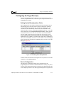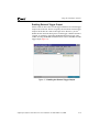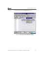
1
R ChipScope Software and ILA Cores User Manual 0401884 (v2.0) December 15, 2000 Software v2001.1 ChipScope Software and ILA Cores User Manual — 0401884 v2.0 Printed in U.S.A. ChipScope Software and ILA Cores User Manual — 0401884 v2.0 R The Xilinx logo shown above is a registered trademark of Xilinx, Inc. ASYL, FPGA Architect, FPGA Foundry, NeoCAD, NeoCAD EPIC, NeoCAD PRISM, NeoROUTE, Timing Wizard, TRACE, XACT, XILINX, XC2064, XC3090, XC4005, XC5210, and XC-DS501 are registered trademarks of Xilinx, Inc. The shadow X shown above is a trademark of Xilinx, Inc. All XC-prefix product designations, A.K.A Speed, Alliance Series, AllianceCORE, BITA, CLC, Configurable Logic Cell, CoolRunner, CORE Generator, CoreLINX, Dual Block, EZTag, FastCLK, FastCONNECT, FastFLASH, FastMap, Fast Zero Power, Foundation, HardWire, IRL, LCA, LogiBLOX, Logic Cell, LogiCORE, LogicProfessor, MicroVia, MultiLINX, PLUSASM, PowerGuide, PowerMaze, QPro, RealPCI, RealPCI 64/66, SelectI/O, SelectRAM, SelectRAM+, Silicon Xpresso, Smartguide, Smart-IP, SmartSearch, Smartspec, SMARTSwitch, Spartan, TrueMap, UIM, VectorMaze, VersaBlock, VersaRing, Virtex, WebFitter, WebLINX, WebPACK, XABEL, XACTstep, XACTstep Advanced, XACTstep Foundry, XACT-Floorplanner, XACT-Performance, XAM, XAPP, X-BLOX, XBLOX plus, XChecker, XDM, XDS, XEPLD, Xilinx Foundation Series, XPP, XSI, and ZERO+ are trademarks of Xilinx, Inc. The Programmable Logic Company and The Programmable Gate Array Company are service marks of Xilinx, Inc All other trademarks are the property of their respective owners. Xilinx, Inc. does not assume any liability arising out of the application or use of any product described or shown herein; nor does it convey any license under its patents, copyrights, or maskwork rights or any rights of others. Xilinx, Inc. reserves the right to make changes, at any time, in order to improve reliability, function or design and to supply the best product possible. Xilinx, Inc. will not assume responsibility for the use of any circuitry described herein other than circuitry entirely embodied in its products. Xilinx, Inc. devices and products are protected under one or more of the following U.S. Patents: 4,642,487; 4,695,740; 4,706,216; 4,713,557; 4,746,822; 4,750,155; 4,758,985; 4,820,937; 4,821,233; 4,835,418; 4,855,619; 4,855,669; 4,902,910; 4,940,909; 4,967,107; 5,012,135; 5,023,606; 5,028,821; 5,047,710; 5,068,603; 5,140,193; 5,148,390; 5,155,432; 5,166,858; 5,224,056; 5,243,238; 5,245,277; 5,267,187; 5,291,079; 5,295,090; 5,302,866; 5,319,252; 5,319,254; 5,321,704; 5,329,174; 5,329,181; 5,331,220; 5,331,226; 5,332,929; 5,337,255; 5,343,406; 5,349,248; 5,349,249; 5,349,250; 5,349,691; 5,357,153; 5,360,747; 5,361,229; 5,362,999; 5,365,125; 5,367,207; 5,386,154; 5,394,104; 5,399,924; 5,399,925; 5,410,189; 5,410,194; 5,414,377; 5,422,833; 5,426,378; 5,426,379; 5,430,687; 5,432,719; 5,448,181; 5,448,493; 5,450,021; 5,450,022; 5,453,706; 5,455,525; 5,466,117; 5,469,003; 5,475,253; 5,477,414; 5,481,206; 5,483,478; 5,486,707; 5,486,776; 5,488,316; 5,489,858; 5,489,866; 5,491,353; 5,495,196; 5,498,979; 5,498,989; 5,499,192; 5,500,608; 5,500,609; 5,502,000; 5,502,440; 5,504,439; 5,506,518; 5,506,523; 5,506,878; 5,513,124; 5,517,135; 5,521,835; 5,521,837; 5,523,963; 5,523,971; 5,524,097; 5,526,322; 5,528,169; 5,528,176; 5,530,378; 5,530,384; 5,546,018; 5,550,839; 5,550,843; 5,552,722; 5,553,001; 5,559,751; 5,561,367; 5,561,629; 5,561,631; 5,563,527; 5,563,528; 5,563,529; 5,563,827; 5,565,792; 5,566,123; 5,570,051; 5,574,634; 5,574,655; 5,578,946; 5,581,198; 5,581,199; 5,581,738; 5,583,450; 5,583,452; 5,592,105; 5,594,367; 5,598,424; 5,600,263; 5,600,264; 5,600,271; 5,600,597; 5,608,342; 5,610,536; 5,610,790; 5,610,829; 5,612,633; 5,617,021; 5,617,041; 5,617,327; 5,617,573; 5,623,387; 5,627,480; 5,629,637; 5,629,886; 5,631,577; 5,631,583; 5,635,851; 5,636,368; 5,640,106; 5,642,058; 5,646,545; 5,646,547; 5,646,564; 5,646,903; 5,648,732; 5,648,913; 5,650,672; 5,650,946; 5,652,904; 5,654,631; 5,656,950; 5,657,290; 5,659,484; 5,661,660; 5,661,685; 5,670,896; 5,670,897; 5,672,966; 5,673,198; 5,675,262; 5,675,270; 5,675,589; 5,677,638; 5,682,107; 5,689,133; 5,689,516; 5,691,907; 5,691,912; 5,694,047; 5,694,056; 5,724,276; 5,694,399; 5,696,454; 5,701,091; 5,701,441; 5,703,759; 5,705,932; 5,705,938; 5,708,597; 5,712,579; 5,715,197; Xilinx Development System 5,717,340; 5,719,506; 5,719,507; 5,724,276; 5,726,484; 5,726,584; 5,734,866; 5,734,868; 5,737,234; 5,737,235; 5,737,631; 5,742,178; 5,742,531; 5,744,974; 5,744,979; 5,744,995; 5,748,942; 5,748,979; 5,752,006; 5,752,035; 5,754,459; 5,758,192; 5,760,603; 5,760,604; 5,760,607; 5,761,483; 5,764,076; 5,764,534; 5,764,564; 5,768,179; 5,770,951; 5,773,993; 5,778,439; 5,781,756; 5,784,313; 5,784,577; 5,786,240; 5,787,007; 5,789,938; 5,790,479; 5,790,882; 5,795,068; 5,796,269; 5,798,656; 5,801,546; 5,801,547; 5,801,548; 5,811,985; 5,815,004; 5,815,016; 5,815,404; 5,815,405; 5,818,255; 5,818,730; 5,821,772; 5,821,774; 5,825,202; 5,825,662; 5,825,787; 5,828,230; 5,828,231; 5,828,236; 5,828,608; 5,831,448; 5,831,460; 5,831,845; 5,831,907; 5,835,402; 5,838,167; 5,838,901; 5,838,954; 5,841,296; 5,841,867; 5,844,422; 5,844,424; 5,844,829; 5,844,844; 5,847,577; 5,847,579; 5,847,580; 5,847,993; 5,852,323; 5,861,761; 5,862,082; 5,867,396; 5,870,309; 5,870,327; 5,870,586; 5,874,834; 5,875,111; 5,877,632; 5,877,979; 5,880,492; 5,880,598; 5,880,620; 5,883,525; 5,886,538; 5,889,411; 5,889,413; 5,889,701; 5,892,681; 5,892,961; 5,894,420; 5,896,047; 5,896,329; 5,898,319; 5,898,320; 5,898,602; 5,898,618; 5,898,893; 5,907,245; 5,907,248; 5,909,125; 5,909,453; 5,910,732; 5,912,937; 5,914,514; 5,914,616; 5,920,201; 5,920,202; 5,920,223; 5,923,185; 5,923,602; 5,923,614; 5,928,338; 5,931,962; 5,933,023; 5,933,025; 5,933,369; 5,936,415; 5,936,424; 5,939,930; 5,942,913; 5,944,813; 5,945,837; 5,946,478; 5,949,690; 5,949,712; 5,949,983; 5,949,987; 5,952,839; 5,952,846; 5,955,888; 5,956,748; 5,958,026; 5,959,821; 5,959,881; 5,959,885; 5,961,576; 5,962,881; 5,963,048; 5,963,050; 5,969,539; 5,969,543; 5,970,142; 5,970,372; 5,971,595; 5,973,506; 5,978,260; 5,986,958; 5,990,704; 5,991,523; 5,991,788; 5,991,880; 5,991,908; 5,995,419; 5,995,744; 5,995,988; 5,999,014; 5,999,025; 6,002,282; and 6,002,991; Re. 34,363, Re. 34,444, and Re. 34,808. Other U.S. and foreign patents pending. Xilinx, Inc. does not represent that devices shown or products described herein are free from patent infringement or from any other third party right. Xilinx, Inc. assumes no obligation to correct any errors contained herein or to advise any user of this text of any correction if such be made. Xilinx, Inc. will not assume any liability for the accuracy or correctness of any engineering or software support or assistance provided to a user. Xilinx products are not intended for use in life support appliances, devices, or systems. Use of a Xilinx product in such applications without the written consent of the appropriate Xilinx officer is prohibited. Copyright 1991-2000 Xilinx, Inc. All Rights Reserved. ChipScope Software and ILA Cores User Manual — 0401884 v2.0 ChipScope Software and ILA Cores User Manual — 0401884 v2.0 Xilinx Development System R Chapter 1 Introduction ChipScope Tools Overview As the density of FPGA devices increases, so does the impracticality of attaching test equipment probes to these devices under test. The ChipScope Analyzer integrates key logic analyzer hardware components with the target design inside the Virtex device. The ChipScope Tools communicate with these components and provide the designer with a complete logic analyzer, without the need for cumbersome probes or expensive test equipment. ChipScope Tools Description The ChipScope Tools include: • the ChipScope Core Generator • the ChipScope Core Inserter, and • the ChipScope Analyzer The Core Generator provides netlists and instantiation templates for the Integrated CONtroller (ICON) core and the Integrated Logic Analyzer (ILA) core. The Core Inserter automatically inserts these two cores into the user’s synthesized design. The Analyzer allows setup and trace display for the ILA core. The ILA core provides the trigger and trace capture capability. The ICON core communicates to the dedicated Boundary Scan pins. The Analyzer supports both the Xilinx MultiLINX™ and Parallel Cable III download cables for communication between the PC and FPGA(s). The MultiLINX cable supports both USB (Windows 98 and Windows 2000) and RS-232 serial communication from the PC (Figure 1). The Parallel Cable III ChipScope Software and ILA Cores User Manual v2.0 December 15, 2000 1-1 R ChipScope Software and ILA Cores User Manual supports only parallel port communication from the PC to the Boundary Scan chain. Target FPGA with ILA Cores User Function User Function PC with ChipScope Tools ILA ILA ChipScope Analyzer User Function JTAG MultiLINX or Parallel Cable III Control ILA JTAG Connection Target Board cs_01_001204 Figure 1: ChipScope Block Diagram Users can place the ILA and ICON cores into their design by: • generating the cores with the Core Generator and instantiating them into the source HDL code, or • inserting the cores into the post-synthesis EDIF netlist using the Core Inserter The design is then placed and routed using the Xilinx Alliance Series™ or Foundation Series™ tools. Next, the user downloads the bitstream and analyzes the design with the ChipScope software Analyzer. The ChipScope Analyzer contains many features that Xilinx FPGA designers need for thoroughly verifying their logic (Table 1-1). User-selectable data channels range from 1 to 256, and the number of sample sizes ranges from 256 to 4096, effectively doubling any FPGA logic analysis capability on the market today. Users can change the triggers in real time without affecting 1-2 v2.0 December 15, 2000 Xilinx Development System R Introduction their logic. The easy-to-use ChipScope Analyzer leads designers through the process of modifying triggers and analyzing the data. Table 1-1 ChipScope Features and Benefits Feature Benefit 1 to 256 user-selectable data channels Accurately captures wide data bus functionality User-selectable sample buffers ranging in size from 256 to 4096 samples Large sample size increases accuracy and probability of capturing infrequent events Separate bus trigger with user-selectable width of 1-64 bits Separate trigger bus reduces need for sample storage All data and trigger operations are synchronous to user clock up to 155 MHz Capable of high-speed data capture Trigger conditions are in-system changeable without affecting user logic No need to single step or stop a design for logic analysis Can write waveforms to VCD, FBDF, and ASCII formats Compatible with Agilent Technologies and other waveform viewers Easy-to-use graphical interface Guides users through selecting the correct options Up to 15 independent ILA capture cores per device Can segment logic and test smaller sections of a large design for greater accuracy Multiple trigger settings Records duration and number of events along with matches and ranges for greater accuracy and flexibility Downloadable from the Xilinx website Tools are easily accessible from the ChipScope Suite ChipScope Software and ILA Cores User Manual v2.0 December 15, 2000 1-3 R ChipScope Software and ILA Cores User Manual Design Flow The ChipScope Tools design flow (Figure 2) merges easily with any standard FPGA design flow that uses a standard HDL synthesis tool and the Alliance Series or Foundation Series implementation tools. Generate ICON and ILA cores using the Core Generator Instantiate ICON and ILA cores into the HDL source Synthesize design Connect buses and internal signals OR... Synthesize design without ILA or ICON core instantiation Insert ICON and ILA cores into synthesized design (EDIF netlist) using Core Inserter Implement Design Download bitstream, trigger, and view waveforms using Chipscope Analyzer ila_figure_2_flow-sa_112900 Figure 2: ChipScope Tools Design Flow 1-4 v2.0 December 15, 2000 Xilinx Development System R Introduction Trigger Settings The ILA core has two trigger modes: basic and extended. The basic trigger mode provides up to two trigger match units capable of detecting a single exact match for every trigger condition. The extended trigger mode adds the ability to do range matching, trigger pulse width duration measurement, trigger event counting, and if-then trigger macros. Table 1-2 compares the basic and extended trigger modes. Table 1-2 Basic and Extended ILA Trigger Modes Basic Mode Extended Mode Up to two match units Yes Yes Trigger function combining all match units Yes Yes Match value and edge comparison Yes Yes Match range comparison (such as >, ≥ <,≤) No Yes Trigger pulse duration measurement No Yes Trigger event count measurement No Yes If-then trigger macros No Yes Trigger Mode Feature External Trigger Description The ChipScope software Analyzer can accept a trigger input signal and generate a trigger output signal for use with external test equipment. An external trigger input signal must enter the device on a normal input pin connected to the ICON core unit where it is distributed to each of 15 possible ILA components in the design. Similarly, each ILA core unit can generate an output signal that is connected to the ICON unit. The ICON unit then logically OR’s all of the external trigger output signals and drives them to a single output pin on the device. Users can enable each ILA core component to drive each respective external trigger output signal to the ICON core component without having to resynthesize the design. ChipScope Software and ILA Cores User Manual v2.0 December 15, 2000 1-5 R ChipScope Software and ILA Cores User Manual Capture Modes Each ILA core can capture data independently from all other ILA cores in the design. Furthermore, the ILA core can capture data using one of two capture modes: one shot and on trigger. The one shot capture mode uses a single trigger event (such as a boolean or macro combination of the individual trigger match unit events) to collect enough data to fill the sample buffer (up to 4096 samples). The trigger position can be set to the beginning of the sample buffer (trigger first, then collect), the end of the sample buffer (collect until the trigger event), or anywhere in between. The on trigger capture mode uses multiple trigger events to perform repetitive measurements on the design under test. Each trigger event can cause a capture of 1 to 16 data samples. These repetitive measurements can continue until the captured data fills the sample buffer. ILA and ICON Core Resource Usage Tables 1-3, 1-4, and 1-5 show the ILA and ICON core resource usage. Table 1-3 1-6 ICON Core CLB Resource Usage Number of Control Ports LUTs Flops Slices Percentage of XCV300 1 68 40 34 1.1 2 103 40 52 1.7 3 138 40 69 2.2 4 171 40 86 2.8 v2.0 December 15, 2000 Xilinx Development System R Introduction Table 1-4 ILA Core CLB Usagea Trigger/ Data Width LUTs Flops Slices Percentage of XCV300 2 57 103 52 1.7 4 60 111 56 1.8 8 66 127 64 2.1 16 78 159 80 2.6 32 105 225 113 3.7 64 154 355 178 5.8 a.This table describes the ILA core with one match unit and the basic trigger function. Table 1-5 ILA Core Block RAM Usagea Data Samples Trigger/ Data Width 256 512 1024 2048 4096 2 1 1 1 1 2 4 1 1 1 2 4 8 1 1 2 4 8 16 1 2 4 8 16 32 2 4 8 16 32 64 4 8 16 32 64 a.This table describes the ILA core with one match unit and the basic trigger function. ChipScope Software and ILA Cores User Manual v2.0 December 15, 2000 1-7 R ChipScope Software and ILA Cores User Manual Synthesis/Insertion Requirements Users can modify many options in the ILA and ICON cores without resynthesizing (in the case of the core generator) or re-inserting (in the case of the core inserter). However, after changing selectable parameters (such as width of the data port or the depth of the sample buffer), the design must be resynthesized either with new cores, or with the cores re-inserted. Table 1-6 describes which design changes require this. Table 1-6 Design Parameter Changes Requiring Resynthesis Design Parameter Change Resynthesis or Re-Insertion Required Change trigger pattern No Running and stopping the trigger No Enabling the external triggers No Changing the trigger signal source Yesa Changing the data signal source Yesa Changing the ILA clock signal Yes Changing the sample buffer depth Yes a.This feature is supported by the Alliance Series 3.1i FPGA Editor and Foundation Series 3.1i FPGA Editor. System Requirements Communications Requirements ChipScope software Analyzer uses either the MultiLINX or Parallel Cable III download cable to communicate with the target devices in Boundary Scan chain of the board-under-test. The MultiLINX cable uses the USB port found on newer PCs and downloads at speeds up to 12 Mb/s throughput. The MultiLINX cable also supports communication through the PC’s RS-232 serial port at speeds up to 57.6 kb/s. MultiLINX also features an adjustable voltage interface that enables it to communicate with systems and I/Os operating at 5V, 3.3V, or 2.5V. The MultiLINX cable is available from Silicon Xpresso™ Cafe (from www.xilinx.com choose Purchase>Programming Cables). 1-8 v2.0 December 15, 2000 Xilinx Development System R Introduction The Parallel Cable III uses the parallel port (i.e., printer port) to communicate with the Boundary Scan chain of the board-under-test. The Parallel Cable III supports only JTAG configuration of target FPGA devices and does not support slave serial configuration. The Parallel Cable III is also available from Silicon Xpresso Cafe (from www.xilinx.com choose Purchase>Programming Cables). Board Requirements For the ChipScope Analyzer and download cable to work properly with the board-under-test, the following board-level requirements must be met: • One or more Virtex, Virtex-E, or Spartan-II target devices must be connected to a JTAG header that contains the TDI, TMS, TCK, and TDO pins • If another device would normally drive the TDI, TMS, or TDI pins of the JTAG chain containing the target device(s), then jumpers on these signals are required to disable these sources, preventing contention with the download cable • If using the MultiLINX download cable, VCC (2.5-5.0V) and GND headers must be available for powering the MultiLINX cable • If using the Parallel Cable III download cable, VCC (2.5-3.3V) and GND headers must be available for powering the Parallel Cable III cable • If the slave-serial configuration mode is to be used by the MultiLINX cable, then a header containing the DIN, CCLK, INIT, PROGRAM, and DONE signals is required • Note that the Parallel Cable III should only be used in JTAG configuration mode. The slave serial flying wires should not be attached to the Parallel Cable III device when used in conjunction with ChipScope Analyzer. ChipScope Software and ILA Cores User Manual v2.0 December 15, 2000 1-9 R ChipScope Software and ILA Cores User Manual Host System Requirements The ChipScope Analyzer runs on any of the following PC systems having these minimum requirements: • Windows 98, Windows 98 SE, or Windows 2000 OS, 32 MB of memory, RS-232 port (MultiLINX), USB port (MultiLINX), or parallel port (Parallel Cable III) • Windows NT 4.0, 64 MB of memory, RS-232 port (MultiLINX) or parallel port (Parallel Cable III) • Java Run-time Environment version 1.1.8 (available for downloading from the ChipScope Suite) Note: In order to use the MultiLINX USB interface under Windows 98 Second Edition or Windows 2000, the correct driver must be used. The updated driver is included in all versions of Xilinx software beginning with 3.1i Service Pack 1. Installing ChipScope Tools The ChipScope Tools include three separate programs: the ChipScope Core Inserter, the ChipScope Core Generator, and the ChipScope Analyzer. After downloading the tools in the form of a self-extracting archive file (ChipScopem-n.exe, where m-n denotes the current version): 1. Select Start>Run. 2. Browse for ChipScopem-n.exe. 3. Click Run. 4. Follow the install wizard instructions. The Analyzer can be installed separately from the Core Inserter and Core Generator. Installing the Java Run-time Environment If you have not already installed the Java Run-time Environment 1.1.8, then download it from the ChipScope Suite the same way you downloaded the ChipScope Tools. Next: 1-10 1. Select Start>Run to run the self-extracting installation file. 2. Browse for the jre1_1_8-win.exe file you just downloaded. v2.0 December 15, 2000 Xilinx Development System R Introduction 3. Click Run. 4. Follow the install wizard instructions. Installing MultiLINX USB Driver for Windows 98 If you need to install the MultiLINX™ cable under Windows 98 or Windows 2000 for USB: 1. Make sure that the PWR and GND wires of the MultiLINX cable are connected to power and ground sources, respectively. 2. Plug the cable into the USB port of the host computer. (An installation dialog box opens.) 3. Click Have Disk. 4. Browse 5. Click OK and follow the installation wizard instructions. the ChipScope Tools installation for the mltlnx.inf file. This is typically installed in folder C:\Program Files\Xilinx\ChipScope\data. Installing the Parallel Cable III Driver ChipScope requires a device driver for the Parallel Cable III to function properly. If you have the Alliance Series or Foundation Series software on the system, the driver is most likely installed. If you need to install the driver, follow these steps: 1. Use Windows Explorer to locate the ChipScope installation (usually C:\Program Files\Xilinx\ChipScope). 2. 3. Open the cableIII folder in the ChipScope installation directory. Run the cableIII installation by double clicking the Setup.exe file in the folder. Setup will guide you through the installation process. cableIII ChipScope Software and ILA Cores User Manual v2.0 December 15, 2000 1-11 ChipScope Software and ILA Cores User Manual 1-12 v2.0 December 15, 2000 R Xilinx Development System R Using the ChipScope Core Generator Chapter 2 Using the ChipScope Core Generator Core Generator Overview The ChipScope Core Generator tool offers users an intuitive graphical user interface to generate the ILA controller core (ICON) and the analyzer (ILA) cores. Once the cores are generated, users can use the instantiation templates (that are provided) to quickly and easily insert the cores into their VHDL or Verilog design. After completing the instantiation and running synthesis, then users implement the design, using the Xilinx implementation tools. Generating an ICON Core The Core Generator gives users the ability to define and generate a customized Integrated CONtroller (ICON) unit to use with one or more Integrated Logic Analyzer (ILA) units in VHDL and Verilog designs. The easy-to-use interface allows users to customize control ports (the number of ILA cores to be connected to the ICON core) and control whether or not to use USER2 Boundary Scan port signals. After the Core Generator validates the user-defined parameters, it generates an EDIF netlist (*.edn) and example code in VHDL and Verilog specific to the synthesis tool used. Users can easily generate the netlist and code examples for use in normal Virtex, Virtex-E, and Spartan-II design flows. The first screen in the Core Generator offers users the choice to generate either an ICON core or an ILA core. Choose ICON (Integrated Controller) core, and click Next. Choosing the File Destination The destination for the ICON EDIF file (icon.edn) is displayed in the Output field. The default directory is the Core Generator install path. To Netlist ChipScope Software and ILA Cores User Manual v2.0 December 15, 2000 2-1 R ChipScope Software and ILA Cores User Manual change it, the user can either type a new path in the field, or select Browse to navigate to a new destination. Entering the Number of Control Ports The ICON core can communicate with up to 15 ILA core units at any given time. However, no ILA core unit may share its control port with any other ILA unit. Therefore, the ICON core needs up to 15 distinct control ports to handle this requirement. Users can select the number of control ports from the Number of Control Ports pull-down list. Enabling the External Triggers Users can configure the ICON core to implement an external trigger input and an external trigger output (i.e. two separate pins) to trigger external test equipment. To enable instantiation of the external input and output trigger pins, select the appropriate Enable External Trigger Input and Enable External Trigger Output check box. If the design does not require external triggers, or if there are no usable pins for triggers, be sure to not check these boxes. If the pins are enabled, then set their IOB location using the following steps: 1. 2. Find the external input and output trigger pad signals in the *.pad file produced by the place and route (par) tool. The signals have the following suffixes: (input) • */U_icon_core/ext_in_pad • */U_icon_core/ext_out_pad (output) Add pin LOC constraints to the *.ucf file so that par correctly places the external trigger pins. Disabling JTAG Clock BUFG Insertion The ICON core communicates to the outside world via the USER1 JTAG scan chain that is clocked by the JTAG clock (TCK). By default, this clock is placed on a global clock resource (BUFG). Checking this box disables that insertion. This should be done only if global resources are very scarce; placing the JTAG clock on regular routing, even high-speed backbone routing, introduces skew. To minimize this skew, make sure the design is adequately constrained. 2-2 v2.0 December 15, 2000 Xilinx Development System R Using the ChipScope Core Generator Including Boundary Scan Ports The BSCAN_VIRTEX primitive has two sets of ports: USER1 and USER2. These provide an interface to the Boundary Scan TAP controller of the Virtex or Virtex-E device. Since the ICON core uses only the USER1 port for communication purposes, the USER2 port signals are available. To use the USER2 interface to the BSCAN_VIRTEX primitive, click the Include Boundary Scan Ports check box. Note: The Boundary Scan ports should be included only if the design needs them. If they are included and not used, some synthesis tools do not connect the ICON core properly which causes errors during the synthesis and implementation stages of development. Choosing the Instantiation Template After choosing the parameters for the ICON core, you can construct an instantiation template. Click Next to view the Sample Code Generation Options, then choose which synthesis tool and language to use. The synthesis tools supported are: • Exemplar LeonardoSpectrum • Synopsys FPGA Compiler • Synopsys FPGA Compiler II • Synopsys FPGA Express • Synplicity Synplify • XST (Xilinx Synthesis Technology) Specifically tailored attributes and options are embedded in the instantiation template for the various synthesis tools. To generate the ICON core without any example files, deselect the Generate Example Files checkbox. Generating the Core After entering the ICON core parameters, click Generate Core to create the netlist and applicable code examples. A message window opens, the progress information appears, and the CORE GENERATION COMPLETE message signals the end of the process. The user can choose to either go back to respecify options or Start Over. ChipScope Software and ILA Cores User Manual v2.0 December 15, 2000 2-3 R ChipScope Software and ILA Cores User Manual Using the ICON Core To instantiate the example ICON core HDL files into your design, use the following guidelines to connect the ICON core port signals to various signals in your design: • Connect one of the ICON core’s unused CONTROL* port signals to a control port of only one ILA core instance in the design. • Leave any unused CONTROL* ports of the ICON core unconnected. (They are removed automatically during the implementation process.) Generating an ILA Core The ChipScope Core Generator gives users the ability to define and generate a customized ILA capture core to use with VHDL and Verilog designs. The easy-to-use interface allows users to customize the maximum number of data sample words stored by the ILA core, the width of the data sample words, and the width of the trigger word (if different from the data word). After the Core Generator validates the user-defined parameters, it generates an EDIF netlist (*.edn) and VHDL and Verilog example code specific to the synthesis tool used. Users can easily generate the netlist and code examples for use in normal Virtex, Virtex-E, and Spartan-II design flows. The first screen in the Core Generator offers users the choice to generate either an ICON or ILA core. Choose ILA (Integrated Logic Analyzer), and click Next. Choosing the File Destination The destination for the ILA EDIF (ila.edn) is displayed in the Output Netlist field. The default directory is the Core Generator install path. To change it, the user can either type a new path in the field, or select Browse to navigate to a new destination. The user can choose from three types of names: a long name in which the options are specified in the component name; a short name (ila.edn); or a custom name for the netlist (the component name will be changed accordingly). Either a long name or a custom name should be chosen if multiple ILA cores with different parameters are used in the design. 2-4 v2.0 December 15, 2000 Xilinx Development System R Using the ChipScope Core Generator The long file name indicates the various parameters specified for the ILA core. Table 2-1 shows the meaning of the abbreviations. Table 2-1 ILA Long Filename Abbreviations Abbreviation Meaning ddx Data Depth of size x dwx Data Width of size x twx Trigger Width of size x t_eq_d Trigger Equals Data ex or bx Extended or Basic Matching with x Units Selecting the Trigger Type To generate the first part of the ILA core, select one of the following trigger types: • Trigger separate from data: The trigger word is completely independent of the data word • Trigger same as data: The trigger and data words are identical. This mode is very common in most logic analyzers, since users can trigger on any bit in the data word being collected. This mode also conserves CLB and routing resources in the ILA core, but limits the data sample word width to the maximum trigger width of 64 bits Selecting the Trigger Match Unit Type An ILA core trigger unit comprises one or more match units that contribute to the overall trigger condition by looking for a specific pattern on the trigger input. The types of patterns and their occurrence over time that are looked for depend on the type of the match unit. The ChipScope core generator handles basic and extended trigger match units. The basic trigger match unit: • Finds only one occurrence of an exact match of a trigger value or edge • Can be used in conjunction with other trigger match units to build the trigger condition boolean equation (using AND/OR) ChipScope Software and ILA Cores User Manual v2.0 December 15, 2000 2-5 R ChipScope Software and ILA Cores User Manual The extended trigger match unit: • Finds one or more occurrences of an exact match of a trigger value or edge • Finds one or more occurrences of a range of trigger values • Detects contiguous (pulse width) or non-contiguous (event count) trigger match conditions over a number of clock cycles • Can be used in conjunction with other trigger match units to build the trigger condition boolean equation (using AND/OR) • Can be used in conjunction with other trigger match units to build the trigger condition macro equation (using IF/THEN) For the ILA core that is being generated, the Trigger Match Unit Type is selected for all match units at the same time. Selecting the Number of Trigger Match Units The number of Trigger Match Units can be set to either one or two. Selecting two trigger match units allows a more flexible trigger condition equation to be a combination of both match units. Selecting one match unit conserves resources while still allowing some flexibility in triggering. Selecting the Data Depth The maximum number of data sample words that the ILA core can store is called the data depth. The data depth determines the number of data width bits contributed by each block RAM unit used by the ILA unit. You can set the data depth to one of five values: 2-6 • Data Depth = 256 samples, data width of one block RAM unit = 16 bits • Data Depth = 512 samples, data width of one block RAM unit = 8 bits • Data Depth = 1024 samples, data width of one block RAM unit = 4 bits • Data Depth = 2048 samples, data width of one block RAM unit = 2 bits • Data Depth = 4096 samples, data width of one block RAM unit = 1 bits v2.0 December 15, 2000 Xilinx Development System R Using the ChipScope Core Generator Entering the Data Width The width of each data sample word stored by the ILA core is called the data width. If the data and trigger words are independent from each other, then the maximum allowable data width depends on the target device type and data depth. However, if the data and trigger words are the same, then the data/trigger width must be any even number in the range of 2 to 64. Selecting the Trigger Width The width of the trigger word used by the ILA core is called the trigger width. If the data and trigger words are independent from each other, then the trigger width can be any even integer in the range of 2 to 64. However, if the data and trigger words are the same, then both the data and trigger widths must be set to any even integer value in the range of 2 to 64. Choosing the Instantiation Template After choosing the parameters for the ILA core, you can construct an instantiation template. Click Next to view the Sample Code Generation Options, then choose which synthesis tool and language to use. The synthesis tools supported are: • Exemplar LeonardoSpectrum • Synopsys FPGA Compiler • Synopsys FPGA Compiler II • Synopsys FPGA Express • Synplicity Synplify • XST (Xilinx Synthesis Technology) Specifically tailored attributes and options are embedded in the instantiation template for the various synthesis tools. To generate the ILA core without any example files, deselect the Generate Example Files checkbox. Generating the Core After entering the ILA core parameters, click Generate Core to create the netlist and applicable code examples. A message window opens, the progress information appears, and the CORE GENERATION COMPLETE message signals the end of the process. The user can choose to either go back to respecify options or Start Over. ChipScope Software and ILA Cores User Manual v2.0 December 15, 2000 2-7 R ChipScope Software and ILA Cores User Manual Using the ILA Core To instantiate the example ILA core HDL files into your design, use the following guidelines to connect the ILA core port signals to various signals in your design: 2-8 • Connect the ILA core’s CONTROL port signal to an unused control port of the ICON core instance in the design. • Connect all unused bits of the ILA core’s data and trigger port signals to “1”. This prevents the mapper from removing the unused trigger and/or data signals and also avoids any DRC errors during the implementation process. • If Trigger Same As Data is selected, connect the data/trigger signal(s) to the ILA core’s DATA port signal. The ILA core’s TRIG port signal is disconnected in this case. In the source code, this port can be connected to the same bus as the DATA port or to all “1”s. • Make sure the data and trigger source signals are synchronous to the ILA clock signal. v2.0 December 15, 2000 Xilinx Development System R Using the ChipScope Core Inserter Chapter 3 Using the ChipScope Core Inserter Core Inserter Overview The ChipScope Core Inserter is a post-synthesis tool for users to generate a netlist that includes the user design as well as ICON and ILA cores, parameterized accordingly. The Core Inserter gives users the flexibility to quickly and easily use the ILA funtionality without resynthesizing the entire design, and without any HDL instantiation. ChipScope Core Inserter Menu Features Working with Projects Core Inserter projects hold all relevant information about source files, destination files, core parameters, and core settings. This allows the user to conveniently store and retrieve information about core insertion between sessions. ChipScope Software and ILA Cores User Manual v2.0 December 15, 2000 3-1 R ChipScope Software and ILA Cores User Manual When the ChipScope Core Inserter is first opened, all the relevant fields are completely blank. Figure 3: Blank Core Inserter Project The condition in Figure 3 can also be achieved by selecting File>New. Opening an Existing Project To open an existing project, select it from the list of recently opened projects, or select File>Open Project, and browse to the project location. When the desired project is located, double-click on it, or select Open. Saving Projects If a project has changed during the course of a session, the user will be prompted to save the project upon exiting the Core Inserter. A project can also be saved by selecting File>Save. To rename the current project or save it to another filename, select File>Save As, type in the new name, and click Save. Exiting the Core Inserter To exit the ChipScope Core Inserter, select File>Exit. If the current project has not been saved, the user will be prompted to save or quit. 3-2 v2.0 December 15, 2000 Xilinx Development System R Using the ChipScope Core Inserter Inserting and Removing ILA Units New ILA units can be inserted into the project by selecting Edit>New ILA Unit. An ILA unit can be removed by selecting Edit>Remove Unit after selecting which ILA unit to delete. Setting Preferences Three external programs (Design Manager, ChipScope Analyzer, and Edif2Ngd) can be called by the ChipScope Core Inserter. The manner in which these programs are called can be altered by selecting Edit>Preferences. Inserting the Cores ICON and ILA Cores are inserted when the flow is completed, or by selecting Insert>Insert Core. If all channels of all the ILA cores are not connected to valid signals, an error message results. Launching Related Tools Both the Xilinx Design Manager and the ChipScope Analyzer can be launched from the ChipScope Core Inserter by selecting Tools>Design Manager or Tools>ChipScope. The locations of these programs can be specified in the Preferences. Specifying Input and Output Files The ChipScope Core Inserter works in a step-by-step process. The first screen you see (Figure 3) shows what needs to be specified first: the input design netlist and constraints file. Click Browse to navigate to the directory where the netlist and constraint files are. The Core Inserter will not write over the netlist or UCF files specified. Instead, a new netlist and UCF will be ChipScope Software and ILA Cores User Manual v2.0 December 15, 2000 3-3 R ChipScope Software and ILA Cores User Manual created with the _ila extension appended by default. Figure 4 shows a project with input and output files specified. When this step is completed, click Next. Figure 4: Core Inserter Project with Files Specified Choosing ICON Options The first options that need to be specified are for the ICON core. The ICON core is the controller core that all ILA units connect to. The ICON core has the options shown in Figure 5. Enable External Trigger Input This option causes a PAD to be added to the design; the pin location specified in Figure 5 is added in the output UCF file specified in Figure 4. This signal is a logical OR’d condition of all the trigger states of all ILA cores in the design. Enable External Trigger Output This option causes a PAD to be added to the design; the pin location specified in Figure 5 is added in the output UCF file specified in Figure 4. This signal can be used in the ChipScope Analyzer to trigger the ILA cores. 3-4 v2.0 December 15, 2000 Xilinx Development System R Using the ChipScope Core Inserter Disable JTAG Clock BUFG Insertion The ICON core communicates to the outside world via the USER1 JTAG scan chain that is clocked by the JTAG clock (TCK). By default, this clock is placed on a global clock resource (BUFG). To disable this insertion, check the Disable JTAG Clock BUFG Insertion box. This should only be done if global resources are very scarce; placing the JTAG clock on regular routing, even high-speed backbone routing, introduces skew. Make sure the design is adequately constrained to minimize this skew. Figure 5 shows a sample of the ICON options. When all ICON options have been set, click Next. Figure 5: ICON Options Choosing ILA Parameters and Options Notice that a new ILA unit has been created in the device hierarchy on the left. The next step is to set up the ILA unit (Figure 6). The top set of parameters specify the Trigger Settings. Trigger Same as Data Use this option when the signals that you want to trigger on are exactly the same signals that you want captured. This option also conserves CLB and routing resources in the ILA core, but limits the data sample word width to the maximum trigger width of 64 bits. This is the common mode with most ChipScope Software and ILA Cores User Manual v2.0 December 15, 2000 3-5 R ChipScope Software and ILA Cores User Manual logic analyzers. Notice that when this option is checked, the Data Width field disappears and Trigger Width is renamed to Trigger/Data Width. Trigger Width This specifies the width of the trigger bus, or the width of the Trigger/Data bus when trigger is the same as data. Valid numbers are even integers from 2 to 64. Data Depth The maximum number of data sample words that the ILA core can store is called the data depth. The data depth determines the number of data width bits contributed by each block RAM unit used by the ILA unit. You can set the data depth to one of five values in the following list: • Data Depth = 256 samples, data width of one block RAM = 16 bits • Data Depth = 512 samples, data width of one block RAM = 8 bits • Data Depth = 1024 samples, data width of one block RAM = 4 bits • Data Depth = 2048 samples data width of one block RAM = 2 bits • Data Depth = 4096 samples, data width of one block RAM = 1 bit Data Width (if necessary) The width of each data sample stored by the ILA core is called the data width. If the data and trigger words are independent from each other, the maximum allowable data width depends on the target device type and data depth, with a maximum of 256. However, if trigger = data, the data/trigger width must be an even number between 2 and 64. Extended Matching If this option is checked, a sophisticated set of match options is available for all match units. The match options include: 3-6 • Finding one or more occurrences of an exact match of a trigger value or edge • Finding one or more occurrences of a range of trigger values • Detecting contiguous (pulse width) or non-contiguous (event count) trigger match conditions over a number of clock cycles v2.0 December 15, 2000 Xilinx Development System R Using the ChipScope Core Inserter • Enabling usage in conjunction with other trigger match units to build the trigger condition boolean equation (using AND/OR) • Enabling usage in conjunction with other trigger match units to build the trigger condition macro equation (using IF/THEN) Basic Matching If Extended Matching is not checked, a subset of the above features are available for all match units, saving CLB usage of the ILA core. These options include: • Finding only one occurrence of an exact match of a trigger value or edge • Enabling usage in conjunction with other trigger match units to build trigger condition boolean equation (using AND/OR) Match Units The number of match units can be set to one or two. Selecting two units allows a more flexible trigger condition equation to be a combination of both match units. Selecting one match unit conserves resources while allowing some flexibility in triggering. Figure 6 shows a sample of the ILA parameters and options. Figure 6: ILA Options and Parameters Choosing Net Connections for ILA Signals The Net Connections box (see Figure 7) under the Match Settings is where the user selects the signals that connect to the ILA core. If trigger is separate from data, then Clock, Trigger, and Data must be specified; when trigger equals data, only Clock and Trigger/Data must be specified. ChipScope Software and ILA Cores User Manual v2.0 December 15, 2000 3-7 R ChipScope Software and ILA Cores User Manual Double-clicking on the Clock Net label or clicking on the plus sign (+) next to it expands into the following (only the Net Connections box is shown): Figure 7: ILA Core Clock Specification Modifying the Clock Connection can be achieved by double-clicking on the CH0: label or highlighting it and clicking Modify Connections. The Select Net dialog box appears (see Figure 8). Figure 8: Select Net Dialog This dialog provides an easy interface to choose nets to connect to the ILA core. All the design’s nets of the given hierarchical level appear in the Nets panel on the right, and the structure of the design can be traversed using the Structure panel on the left. Net names can be filtered for key phrases using the Pattern text box and Filter button. Once the net has been found, click Select to choose it and return to the main Core Inserter window. 3-8 v2.0 December 15, 2000 Xilinx Development System R Using the ChipScope Core Inserter All the nets for Trigger and Data must be chosen in this fashion. Once all the nets have been chosen for a given bus, the ILA bus name changes from red to black (see Figure 9 ). Figure 9: Specifying Data Connections Once all the Clock, Trigger, and Data nets are specified, click Next. A dialog appears asking if you want to proceed with Core Insertion. If Yes is chosen, the cores will be generated, inserted into the netlist, and a .ngo file is created by running the edif2ngd program. Details of this process can be viewed in the Messages panel at the bottom of the window. A Core Generation Complete message in the Messages panel signals success. Adding ILA Units Each device can support up to 15 ILA units (the number of units may also be restricted by block RAM availability and ILA unit parameters). Additional units can be added to the project by selecting Edit>New ILA Unit, or going to the ICON Options window by clicking on ICON in the tree on the left panel (see Figure 5) and selecting the New ILA Unit button. Parameters for the additional ILA units are set up using the same procedure as above. ChipScope Software and ILA Cores User Manual v2.0 December 15, 2000 3-9 ChipScope Software and ILA Cores User Manual 3-10 v2.0 December 15, 2000 R Xilinx Development System R Using the ChipScope Analyzer Chapter 4 Using the ChipScope Analyzer Analyzer Overview The ChipScope Analyzer tool interfaces directly to the ILA and ICON cores. Users can configure their device, choose triggers, and view the results of the capture on the fly. The waveforms and triggers can be manipulated in many ways, providing an easy and intuitive interface to determine the functionality of the design. Analyzer Menu Features Selecting a Device/ILA Unit A single target device (i.e., a Virtex, Virtex-E, or Spartan-II device) can contain up to 15 ILA units. The host communicates through a separate ChipScope Analyzer window for each ILA unit. You can select the current ILA unit only after you connect to the download cable and detect the Boundary Scan chain. Select File>New ILA Unit>Unit n (where n is the ILA unit number) to choose a specific ILA unit. Note that the ILA unit number corresponds to the control port the ILA core is connected to in the case of instantiation, or the Unit ChipScope Software and ILA Cores User Manual v2.0 December 15, 2000 4-1 R ChipScope Software and ILA Cores User Manual number in the case of Core Insertion. Figure 10 shows how ILA Unit 1 is selected. Figure 10: Selecting New ILA Unit If the Boundary Scan chain contains multiple devices that can serve as ILA targets, then select communication to one of the 15 possible ILA units in the target device using File>New ILA Unit>Device m>Device m Unit n (where m is the target device number n is the ILA unit number). Note that the ILA unit number corresponds to the control port number of the ICON unit to which the ILA component is connected, or the Unit number in the case of Core Insertion. Figure 11 shows how to select ILA Unit 0 in target Device 1. If the trigger setup toolbar is not present in the current ChipScope window, then selecting a new ILA unit using this method simply refocuses the current window to the new ILA unit. However, if you select a new ILA unit after you have set up the trigger for the current one, a new ChipScope window opens. 4-2 v2.0 December 15, 2000 Xilinx Development System R Using the ChipScope Analyzer This feature allows you to view the waveforms of multiple ILA units at the same time. Figure 11: Selecting New ILA Unit in Target Device 1 New ILA units are displayed in their own window and the Device/Unit for a particular window is displayed in the title bar. All the ILA units may be triggered at the same time by configuring each trigger in turn. There is no current way to combine the waveform display or trigger setup amongst separate ILA units. ChipScope Software and ILA Cores User Manual v2.0 December 15, 2000 4-3 R ChipScope Software and ILA Cores User Manual Working with Projects Projects hold important information about the ChipScope program state, such as signal naming, signal ordering, bus configurations, and trigger conditions. They allow you to conveniently store and retrieve this information between Analyzer sessions When you first run the ChipScope Analyzer tool, the Select Project dialog box (Figure 12) opens, allowing you to create a new project or open an existing project. Figure 12: Selecting a Project Creating A New Project To create a new project, select Create a new Project (Figure 12) and click OK. In the Choose New Project File dialog box (Figure 13), enter a new project filename name (using the .cpj extension) and click Open. Figure 13: Creating a New Project 4-4 v2.0 December 15, 2000 Xilinx Development System R Using the ChipScope Analyzer Opening An Existing Project To open an existing project, select it from the list of recently opened projects. To browse through all available project files, select More Projects. When you locate the desired project click Open. Saving Projects Projects are automatically saved when you exit the ChipScope software. To rename the current project, or to save a copy to another filename, select File>Save Project As (Figure 14), type the new name in the dialog box, and click Save. Figure 14: Saving a Project Importing and Exporting Only VCD waveforms can be imported. You can import the waveform display from a VCD file and export to VCD, FBDF, and ASCII files. The VCD format is a common waveform viewer file format and the FBDF format is compatible with the Agilent Technologies’ 16700 Series logic analyzers. The ASCII format is a text-only list format that is well suited to a script parser or spreadsheet import. To import a waveform, select File>Import Waveform. A dialog box opens, allowing you to browse for waveform files. After locating and selecting the desired file, click Open. The waveform display in the ChipScope window now contains the imported waveform. You can export a waveform file in a similar fashion. To export the waveform to a VCD file, select File>Export Waveform>VCD Export. To export the ChipScope Software and ILA Cores User Manual v2.0 December 15, 2000 4-5 R ChipScope Software and ILA Cores User Manual waveform to a FBDF file, select File>Export Waveform>FBDF Export. To export the waveform to an ASCII file, select File>Export Waveform>ASCII Export. In each case, a dialog box opens and you can browse for the desired storage folder location. After finding the target location and entering the waveform file name, click Save. The waveform is now stored in the desired format. Closing and Exiting ChipScope To close a ChipScope window, select File>Close. To exit the ChipScope program, select File>Exit. In both cases, if you have not stored the waveform, a dialog box opens, asking if you want to store the current waveform before closing/exiting. If you select Yes, another dialog box opens, from which you can save the waveform. The difference between closing and exiting is: closing closes the current ChipScope window; exiting closes all ChipScope windows and ends the program. However, if only one ChipScope window is open, closing and exiting have the same effect. Opening and Closing a MultiLINX Connection You can connect the MultiLINX cable to the host computer by using a serial communications port (e.g., COM1), the USB (Universal Serial Bus) port connection, or both. However, only one connection to the MultiLINX cable is supported at a time. 4-6 v2.0 December 15, 2000 Xilinx Development System R Using the ChipScope Analyzer Opening a Serial Port MultiLINX Connection If the MultiLINX cable connects to the host computer by way of the serial port, then select Communication>Open Serial Port (Figure 15). Figure 15: Opening a Serial Port Connection to MultiLINX After you select Communication>Open Serial Port, a small dialog box opens (Figure 16). Enter the proper serial port name, select the baud rate for the serial port connected to the MultiLINX cable, then click OK. Make sure you select a port that is not in use by another resource. Figure 16: Selecting a Serial Port When the connection opens, a success message appears in the status bar at the bottom of the ChipScope window. At this point, ChipScope queries the ChipScope Software and ILA Cores User Manual v2.0 December 15, 2000 4-7 R ChipScope Software and ILA Cores User Manual Boundary Scan chain to determine its composition (see “Configuring the Target Device(s)” on page 11). If the MultiLINX connection fails to open, a dialog box opens, notifying you of the problem. Opening a USB Port MultiLINX Connection If the MultiLINX cable connects to the host computer by way of the USB port, then select Communication>Open USB Port (Figure 17). When the connection opens, a success message appears in the status bar at the bottom of the ChipScope window. At this point, ChipScope queries the Boundary Scan chain to determine its composition (see “Configuring the Target Device(s)” on page 11). If the MultiLINX connection fails to open, a dialog box opens, notifying you of the problem. Figure 17: Opening a USB Connection to MultiLINX Closing the MultiLINX Connection Select Communication>Close Port to close the connection to the MultiLINX cable. You must re-establish a connection to the MultiLINX cable before any communication between the ChipScope program and the ILA units in the target device can resume. 4-8 v2.0 December 15, 2000 Xilinx Development System R Using the ChipScope Analyzer Getting MultiLINX Cable Information You can upload information pertaining to the MultiLINX cable (such as the hardware version, memory size, etc.) by selecting Communication>Get Cable Information. See the sample dialog in Figure 18 for the MultiLINX cable information. Figure 18: Getting Cable Information Running MultiLINX Cable Diagnostics To verify that the MultiLINX cable is properly connected to and communicating with the host computer, select Communication>Run Diagnostics. A dialog box opens, reporting whether or not the cable is functioning properly. You can also quickly verify that the MultiLINX cable is communicating with the host computer by turning the LED on the MultiLINX cable on and off. To do this, select the Communication>LED On and Communication>LED Off, respectively. ChipScope Software and ILA Cores User Manual v2.0 December 15, 2000 4-9 R ChipScope Software and ILA Cores User Manual Opening a Parallel Cable III Connection ChipScope supports the Parallel Cable III (HW-JTAG-PC). To open a connection to the Parallel Cable III, make sure the cable is connected to one of the computer’s parallel ports. Select Communication>Parallel Cable (Figure 19). ChipScope prompts you for the port name. Type the printer port name in the port selection box (usually the default LPT1 is correct) and click OK. If successful, ChipScope queries the Boundary Scan chain to determine its composition (see “Configuring the Target Device(s)” on page 11). If ChipScope returns the error message Failed to Open Communication Port, verify that the Parallel Cable III is connected to the correct LPT port. If you have not installed the Parallel Cable III driver, follow the instructions in “Installing the Parallel Cable III Driver” on page 11 in Chapter 1 to install the required device driver software. Figure 19: Opening a Parallel Cable III Connection 4-10 v2.0 December 15, 2000 Xilinx Development System R Using the ChipScope Analyzer Configuring the Target Device(s) You can use ChipScope software with one or more target devices (Virtex, Virtex-E, or Spartan-II FPGAs). The first step is to set up all of the devices in the Boundary Scan chain. Setting Up the Boundary Scan Chain Once ChipScope has successfully communicated with a download cable, it automatically queries the JTAG chain to find its composition. All Xilinx Virtex/E/EM, Spartan-II, Spartan-XL, 9500/XL/XV, 4000XL/XLA, and 18V00 devices are automatically detected. The entire IDCODE can be verified for Virtex, Virtex-E, Virtex-EM, and Spartan-II devices. To view the chain composition, select Configure>Boundary Scan Setup. A dialog appears with all detected devices in order. For devices that are not automatically detected, the IR (Instruction Register) length must be specified to insure proper communication to the ILA and ICON cores This information can be found in the device’s BSDL file. The following example has a CoolRunner CPLD, XC18V02 PROM, and Virtex V150 in a chain. A non-zero IR length must be specified for the unknown (CoolRunner) device in order to close the dialog (see Figure 20). Figure 20: Boundary Scan Setup Window UserID’s can be read out of the ILA target devices (only the XCV150 in this example) by selecting Read User IDs. Device Configuration The method for configuring the target device depends on how the programming device connects to the download cable. Currently, only JTAG and Slave-Serial programming modes are supported for the MulitLINX cable by the ChipScope software. Only JTAG programming mode is supported for ChipScope Software and ILA Cores User Manual v2.0 December 15, 2000 4-11 R ChipScope Software and ILA Cores User Manual the Parallel Cable III download cable. If the target device is to be programmed using the MultiLINX cable by way of the Slave-Serial port, select Configure>Slave-Serial Mode (Figure 21). Figure 21: Configuring Using Slave-Serial Mode 4-12 v2.0 December 15, 2000 Xilinx Development System R Using the ChipScope Analyzer If the target device is to be programmed using the MultiLINX or Parallel Cable III download cable by way of the JTAG port, select Configure>JTag Mode (Figure 22). Figure 22: Configuring JTAG Mode Window After selecting the configuration mode, the Configuration Selection dialog box (Figure 23) opens. This dialog reflects the configuration choice, and defaults to a blank entry for the configuration file. ChipScope supports MCS, BIT, and RBT files as inputs. Figure 23: Selecting a Part ChipScope Software and ILA Cores User Manual v2.0 December 15, 2000 4-13 R ChipScope Software and ILA Cores User Manual To select the BIT file to download, click on Select New File. The Open Configuration File dialog box (Figure 24) opens. Using the browser, select the device file you want to use to configure the target device. It is important to select a BIT file generated with the proper BitGen settings. For example, if the target device is configured using the JTAG port, then use the BitGen option -g StartupClk:JtagClk when creating the configuration file. Do not use this BitGen option if the target device is configured using slave-serial mode. Once you locate and select the proper device file, click Open to return to the Configuration Selection dialog. Figure 24: Opening a Configuration File Once the mode and BIT file have been chosen, click OK to configure the device. Observing Configuration Progress While the device is being configured, the status of the configuration is displayed at the bottom of the ChipScope window. If using the MultiLINX cable, first the cable is initialized for the type of configuration download being performed. Next, the progress of the bitstream download is displayed. If the DONE status is not displayed, a dialog box opens, explaining the problem encountered during configuration. If the download is successful, the target device is automatically queried for the ILA core, and the Trigger Setup toolbar is displayed. 4-14 v2.0 December 15, 2000 Xilinx Development System R Using the ChipScope Analyzer Displaying JTAG ID Codes One method of verifying that the target device was configured correctly is to upload the device and user-defined ID codes from the target device. For instance, to upload and display the user-defined ID code (i.e., the 8-digit hexadecimal code that can be set using the BitGen option -g UserID), select Configure>Show USERCODE (Figure 25). Use Configure>Show IDCODE to display the fixed device ID code. Figure 25: Uploading User-Defined ID Code The ID codes are displayed in a small dialog box (Figure 26). Figure 26: Viewing User-Defined ID Code ChipScope Software and ILA Cores User Manual v2.0 December 15, 2000 4-15 R ChipScope Software and ILA Cores User Manual Opening the Trigger Setup Toolbar To set up the trigger for a device that has already been configured with a design containing an ILA core, select Data>Trigger Setup (Figure 27). Figure 27: Opening the Trigger Setup Toolbar After you select Trigger Setup, the ChipScope program queries the ILA unit to determine the proper settings for the trigger setup. If the device has just been configured, then it is queried and the Trigger Setup toolbar appears automatically. 4-16 v2.0 December 15, 2000 Xilinx Development System R Using the ChipScope Analyzer The parameters associated with the ILA unit appear at the bottom of the ChipScope Analyzer window (see Figure 28 for example of Trigger Width: 8, Signal Count: 16, Data Depth: 2048, ILA Core Version 1.1 extended match units). The Trigger Width, Signal Count, Data Depth, and Extended Features parameters correspond to the ILA core parameters used when the core is generated. Figure 28: Viewing the Trigger Setup Toolbar Setting Up the Trigger The trigger mechanism inside each ILA core can be modified at run-time without having to re-compile the design. The following sections describe how to modify the various components that make up the trigger mechanism. Basic Match Unit Comparison Values The match units are called Mn (where n is 0 or 1, depending on the number of trigger match units in the ILA core) and can be one of two types: basic or extended. If the match units are basic, then you can change only the comparison value (Figure 29). You can set each bit of the match unit to one of the following values: • X : Any value (logical zero or logical one) • 0 : Logical zero only • 1 : Logical one only • R : Rising edge only • F : Falling edge only • B : Both edges (rising edge or falling edge) You can set match word values by clicking on each bit until the desired value appears, or by clicking on the bit value and typing the desired value. Moving ChipScope Software and ILA Cores User Manual v2.0 December 15, 2000 4-17 R ChipScope Software and ILA Cores User Manual the cursor over (but not clicking on) a bit in the match word causes a tool tip window to appear that indicates the bit position and current match value. Figure 29: Setting the Basic Match Comparison Value 4-18 v2.0 December 15, 2000 Xilinx Development System R Using the ChipScope Analyzer Extended Match Unit Comparison Value If the match unit Mn (where n is 0 or 1, depending on the number of trigger match units in the ILA core) is an extended match unit, then you can configure both the comparison type and value during trigger setup (Figure 30). Figure 30: Setting the Extended Match Comparison Type and Value The possible comparison types are: • • • • • • = : equal to <> : not equal to > : greater than >= : greater than or equal to < : less than <= : less than or equal to ChipScope Software and ILA Cores User Manual v2.0 December 15, 2000 4-19 R ChipScope Software and ILA Cores User Manual The possible match comparison bit values depend on the comparison type. For instance, when the comparison type is set to ‘=’, you can set each bit of the comparison value to one of the following: • X : Any value (logical zero or logical one) • 0 : Logical zero only • 1 : Logical one only • R : Rising edge only • F : Falling edge only • B : Both edges (rising edge or falling edge) If the comparison type is set to something other than “=”, then you can set each bit of the comparison to one of the following: • 0 : Logical zero only • 1 : Logical one only You can set the match word values by clicking on each bit until the desired value appears, or by clicking on the bit value and typing the desired value. If you move the cursor over a bit in the match word and do not click, a tool tip dialog box opens displaying the bit position and current match value. 4-20 v2.0 December 15, 2000 Xilinx Development System R Using the ChipScope Analyzer Setting Up Pulse Width and Event Count You can configure an extended match unit to find matches that occur over one or more clock cycles contiguously (in a row) or non-contiguously (not necessarily in a row). If the match conditions must remain satisfied during a specific number of contiguous clock cycles, then the match Pulse Width Duration must be measured. If it only needs to occur for a specific number of clock cycles (not necessarily in a row), then the Match Event Count must be measured. To measure the Pulse Width Duration, click Width (Figure 31). The match condition is true only if the match condition value is detected for at least n clock cycles in a row (where n can be any value from 1 to 65,536). For a subsequent occurrence of the match condition to become satisfied, the match condition “pulse” must return to its non-active state in order to reset the Pulse Width Duration detection logic. Figure 31: Selecting the Pulse Width Duration ChipScope Software and ILA Cores User Manual v2.0 December 15, 2000 4-21 R ChipScope Software and ILA Cores User Manual To measure the Trigger Event Count, click Count (Figure 32). The match condition is true only if the match condition value is detected for at least n clock cycles not necessarily in a row (where n can be any value from 1 to 65,536). The match condition Trigger Event Count automatically resets after the match condition is satisfied. Figure 32: Selecting the Trigger Event Count 4-22 v2.0 December 15, 2000 Xilinx Development System R Using the ChipScope Analyzer Setting Up a Boolean Trigger Condition The Trigger Condition field describes how the match units (M0, M1) and the external trigger input (EXT) can be combined to form an overall trigger condition. Both basic and extended trigger match units can build boolean equations from the available match units and the external trigger input to form the overall trigger condition. Select the boolean trigger condition type by choosing Boolean from the pull-down menu (not available in the “basic” trigger match type case). To designate the equation, click the buttons to the immediate right of the field in the trigger setup toolbar. For instance, if you want the trigger condition boolean equation to be “not M0 or EXT” (Figure 33), do the following: Trigger Condition • Click twice on the first button to select !M0 (i.e., not M0). • Click once on the third button to select EXT • Click once on the middle button that reads AND to select OR Clicking the button until it is blank effectively removes the match condition or external trigger input out of the boolean equation. Figure 33: Selecting the Boolean Trigger Condition ChipScope Software and ILA Cores User Manual v2.0 December 15, 2000 4-23 R ChipScope Software and ILA Cores User Manual Setting Up a Macro Trigger Condition Only the extended trigger match units can build “if-then” macro equations out of the available match units and the external trigger input to form the overall trigger condition. Select the macro trigger condition type by selecting the “macro” type from the pull-down menu. An example of the “if-then” macro condition is “if M0 is satisfied, and then ~EXT is satisfied, then the overall trigger condition is satisfied.” To designate the macro equation, click on the buttons to the immediate right of the Trigger Condition field in the trigger setup toolbar. For instance, if you want the trigger condition boolean equation to be “M0 then not EXT” (Figure 34), do the following: • Click the third button four times to select !EXT (i.e., not EXT). • Click the first button one time to select M0 • The middle button is automatically set to THEN Clicking the first and/or third button until it is blank effectively removes the match condition or external trigger input from the macro equation. However, use the boolean equation if neither condition in the macro equation is used. Figure 34: Selecting the Macro Trigger Condition 4-24 v2.0 December 15, 2000 Xilinx Development System R Using the ChipScope Analyzer Selecting One Shot Capture Mode The One Shot capture mode captures an entire sample buffer of data once the trigger condition is satisfied. This capture method allows you to capture data both before and after the trigger condition is satisfied. Click One Shot in the trigger toolbar (Figure 35) to select the One Shot capture mode. During the One Shot capture mode, you can set the trigger position to anywhere from the beginning of the capture buffer (Position = 0) to the end of the capture buffer (Position = Sample Depth -1). To set the trigger position, click inside the box to the right of the Position setting on the trigger toolbar, (Figure 35). For example, if the trigger position is set to 1000, then the 1000 data samples captured before the trigger condition is satisfied are displayed along with 1047 samples captured after the trigger. Figure 35: Selecting One Shot Capture Mode ChipScope Software and ILA Cores User Manual v2.0 December 15, 2000 4-25 R ChipScope Software and ILA Cores User Manual Selecting On Trigger Capture Mode The On Trigger capture mode continues capturing data after each trigger condition is satisfied, until the entire sample buffer is full. You can set the number of samples captured per trigger to any value from 1 to 16. To select this mode, click On Trigger in the trigger toolbar (Figure 36). Select the number of samples per trigger from the Samples per Capture scrolling list box on the trigger toolbar (Figure 36). For example, if you select the trigger position 8, then 8 data samples are captured after each occurrence of the trigger condition until the ILA unit’s capture storage resources are completely full. In some cases, the last occurrence of the trigger condition might result in fewer samples stored, depending on the value of the Samples per Capture setting and the sample depth of the ILA unit. Figure 36: Selecting On Trigger Capture Mode Window 4-26 v2.0 December 15, 2000 Xilinx Development System R Using the ChipScope Analyzer Enabling External Trigger Output Each ILA unit can drive out its overall trigger condition as an external trigger output to the ICON unit. There it is logically OR’ed with the external trigger output of all the other ILA units in the target device. However, you can disable the ILA unit from driving out its overall trigger condition (and drive a logical “0” instead) by deselecting the Ext. Out field in the trigger setup toolbar. Selecting the Ext. Out field enables the ILA unit’s individual external trigger output (Figure 37). Figure 37: Enabling the External Trigger Output ChipScope Software and ILA Cores User Manual v2.0 December 15, 2000 4-27 R ChipScope Software and ILA Cores User Manual Capture Status Window After you arm the trigger by selecting Run/Stop>Run, the status of the ILA unit appears in the Sample Buffer display area with one of the following values: • ARMED : The trigger is currently armed and waiting for an occurrence of the trigger condition. • <value> : A number <value> between 1 and Sample Depth - 1 that represents how many data samples have currently been captured. • FULL : The capture storage is full and the capture process has ended. • STOPPED : The ILA unit has been halted by the act of stopping the acquisition. During One Shot capture mode, once the ILA unit progresses from the ARMED state to the FULL state, ChipScope program automatically displays the captured data in the waveform window (Figure 38). Note that the X-axis of the waveform is measured in number of data samples. Data sample 0 is always at the location of the trigger condition. Figure 38: Viewing the One Shot Capture Mode Waveform 4-28 v2.0 December 15, 2000 Xilinx Development System R Using the ChipScope Analyzer During On Trigger capture mode, once the ILA unit progresses from the ARMED state to the FULL state, the ChipScope program automatically displays the captured data in the waveform window (Figure 39). Data sample 0 is always at the location of the first trigger condition. Figure 39: Viewing the On Trigger Capture Mode Waveform ChipScope Software and ILA Cores User Manual v2.0 December 15, 2000 4-29 R ChipScope Software and ILA Cores User Manual Running and Stopping the Trigger Running/Arming the Trigger After setting up the trigger, select Run/Stop>Run to arm it. The trigger stays armed until the trigger condition is satisfied or the user disarms the trigger. Once the trigger condition is satisfied, the trigger automatically disarms and the captured data appears in the waveform window. To force the trigger, select Run/Stop>Trigger Immediate. This causes the ILA unit to ignore the trigger condition and trigger immediately. After the sample buffer fills with data, the trigger disarms and the captured data appears in the waveform window. Stopping/Disarming the Trigger To disarm the trigger, select Run/Stop>Stop Acquisition. If the trigger condition has been satisfied at least once before the acquisition is stopped, the ChipScope program disarms the trigger and displays the captured data. Subsequent selections of Run/Stop>Run cause the trigger to re-arm. Using Buses and Signals Grouping Signals Into a Bus You can group up to 64 signals to form a bus. Hold down the shift key and use the mouse to select one or more ungrouped signals in the Bus/Signal display, then select Bus/Signal>Group Into Bus. When the text input box opens, enter a name for the new bus, then click Enter. Names must be unique and may contain only letters, numbers, and underscores (Figure 40). Figure 40: Grouping Signals into a Bus 4-30 v2.0 December 15, 2000 Xilinx Development System R Using the ChipScope Analyzer Ungrouping Signals From a Bus To ungroup a signal from a bus, highlight a bus in the Bus/Signal display window, then select Bus/Signal>Ungroup From Bus. This removes the bus and places all its signals in the root level (Figure 41). Figure 41: Ungrouping Signals from a Bus Moving Buses and Signals To move buses and signals up and down in the display, highlight a signal or bus, then select Bus/Signal>Move Up or Bus/Signal>Move Down. When the position of a signal in a bus is changed, the bus values are recalculated and the new values appear in the wave display window (Figure 42). Buses and signals can also be moved by dragging and dropping them in the left hand signal pane. Figure 42: Moving Buses and Signals ChipScope Software and ILA Cores User Manual v2.0 December 15, 2000 4-31 R ChipScope Software and ILA Cores User Manual Changing Bus and Signal Names To rename buses and signals anytime for easy identification, click on the bus or signal to rename, then select Bus Signal>Rename. A text input box (Figure 43) opens, prompting for the new name. Names must be unique and may contain letters, numbers, or underscores. Type the new name, then click Enter. Figure 43: Changing Bus and Signal Names 4-32 v2.0 December 15, 2000 Xilinx Development System R Using the ChipScope Analyzer Bus Radix Display Buses can be configured individually to display different radixes in the wave display window. Available bus display options are: hexadecimal, binary, signed decimal, unsigned decimal, octal, ASCII, and Token. By default, bus values are displayed in hexadecimal. ASCII is only available when the bus specified is exactly 8 bits wide. To set the radix for a bus, select a bus in the Bus/Signal panel, then select Bus/Signal>Show As. The menu popup (Figure 44) allows you to choose from the available bus radix options. Figure 44: Changing Bus Display Radix ChipScope Software and ILA Cores User Manual v2.0 December 15, 2000 4-33 R ChipScope Software and ILA Cores User Manual Using Tokens Tokens are string labels that can be assigned to a particular bus value. These labels can be very useful in such applications as address decoding and state machines. Tokens are defined in a separate ASCII file, and loaded into the ChipScope Analyzer when appropriate. The token file itself (.tok extension) has a very simple format, and can be created or edited in any text editor. An example token file is provided in the token directory in the ChipScope install path (Figure 45). Figure 45: Example Token File Tokens are chosen by selecting a bus, then choosing Bus/Signal>Load Tokens. A dialog opens and the user can choose the token file. Once the tokens are loaded, selecting Bus/Signal>Show As>Token enables the tokens for that particular bus. If the bus is wider than the tokens specify (such as choosing 4-bit tokens for an 8-bit bus) the upper bits are assumed 0 for the tokens to 4-34 v2.0 December 15, 2000 Xilinx Development System R Using the ChipScope Analyzer apply. Figure 46 shows such a waveform, with the example file in Figure 45 applied to a 5-bit bus. Figure 46: Example Waveform with Tokens Bus Bit Ordering The bits in each bus can be ordered top to bottom, or bottom to top, when computing their value in the wave display window. To place the most significant bit at the bottom, select Bus/Signal>Bus Bit Ordering>Bottom(MSB) To Top(LSB). To place the most significant bit at the top, select Bus/Signal>Bus Bit Ordering>Top(MSB) To Bottom(LSB). The default bit ordering is bottom to top (Figure 47). Figure 47: Changing Bus Bit Ordering ChipScope Software and ILA Cores User Manual v2.0 December 15, 2000 4-35 R ChipScope Software and ILA Cores User Manual Signal Channel Number Display Channel number display can be toggled to identify which of the ILA core data channels is connected to each of the signals in the waveform display. To toggle the display, select Bus/Signal>Channel Numbers. By default, channel number display is turned off (Figure 48). Figure 48: Enabling Signal Channel Number Display Bus and Signal Coloring Separate colors can be assigned to each bus and signal in the waveform display. To choose a color, highlight the signal or bus, then select Bus/Signal>Color. A color palette opens from which a discrete or customer 4-36 v2.0 December 15, 2000 Xilinx Development System R Using the ChipScope Analyzer color can be chosen in a variety of ways. A bus and its component signals can have different colors (Figure 49). Figure 49: Selecting a Waveform Color ChipScope Software and ILA Cores User Manual v2.0 December 15, 2000 4-37 R ChipScope Software and ILA Cores User Manual Navigating the Waveform Window(s) Centering the Waveform Center the waveform display around a specific point in the waveform by selecting Data>Go To, then centering the waveform display around the X and O markers, as well as the first trigger position (Figure 50). Figure 50: Centering the Waveform Display 4-38 v2.0 December 15, 2000 Xilinx Development System R Using the ChipScope Analyzer Zooming In and Out Select Data>Zoom In to zoom in to the center of the waveform display (Figure 51). Figure 51: Zooming in to the Center of the Waveform Display ChipScope Software and ILA Cores User Manual v2.0 December 15, 2000 4-39 R ChipScope Software and ILA Cores User Manual You can also zoom in to a specific place in the waveform. For example, select Data>Zoom In To>X Marker to zoom in to the X cursor location (Figure 52). Other zoom locations include the O cursor and first trigger position (that is, data sample 0). To zoom in to a specific area of the waveform, select Data>Zoom Area, then click the left mouse button and drag to select an area of the waveform display. Using this method, the waveform display zooms in to the selected area. Figure 52: Zooming in to the X-Marker of the Waveform Display 4-40 v2.0 December 15, 2000 Xilinx Development System R Using the ChipScope Analyzer To zoom out from a waveform, use Data>Zoom Out (Figure 53). Figure 53: Zooming out from the Waveform Display ChipScope Software and ILA Cores User Manual v2.0 December 15, 2000 4-41 R ChipScope Software and ILA Cores User Manual To view the entire waveform display select Data>Fit Window (Figure 54), Figure 54: Fitting the Waveform Display in the Window Toggling Time/State Display The x-axis of the waveform can be displayed as the sample number relative to the trigger event (default) or by a time unit per sample starting at the first sample captured. By default, the time unit is 5ns/sample. Setting a Sample Clock Period When the waveform is viewed with the x-axis in time units, the sample clock period can be modified with this option. Units are always in ns. 4-42 v2.0 December 15, 2000 Xilinx Development System R Using the ChipScope Analyzer Plot Values This option brings up a separate window, with a bus or buses plotted in an x-y format. Two line types can be chosen: a scatter plot, which plots a single dot at each data point, and a line plot, which connects all the data points together with a line. Separate buses are displayed in separate colors (see Figure 55, with line graph chosen). Figure 55: Example of X-Y Plot Generating a Demo Waveform To generate a sample waveform for trying out various ChipScope features without using actual hardware, select Data>Demo Waveform. Changing Waveform Window Focus If more than one ILA unit ChipScope window is open, use Window>Unit n (where n is the ILA unit number) to change focus between the windows. Viewing the Help Pages The ChipScope help pages contain only the currently opened versions of the ChipScope software and each of the ILA core units. Selecting Help>About: ChipScope Software displays the version of the ChipScope software. Selecting Help>About: ILA Core displays the versions of all of the open ILA units. ChipScope Software and ILA Cores User Manual v2.0 December 15, 2000 4-43 R ChipScope Software and ILA Cores User Manual ChipScope Main Toolbar Features In addition to the menu options, other ChipScope commands are available on a toolbar residing directly below the ChipScope menu (Figure 56). Figure 56: Main ChipScope Toolbar Display The toolbar buttons (from left to right) correspond to the following equivalent menu options: • Open Cable/Search JTAG Chain : automatically detects the cable, and queries the JTAG chain to find its composition • Configure with Last Used Settings : Configure>Slave Serial (whichever 4-44 same as Configure>JTAG or was last used) • Trigger Setup : same as Data>Trigger Setup • Run : same as Run/Stop>Run (F5) • Stop : same as Run/Stop>Stop (F9) • Trigger Immediate • Go To X Marker : same as Data>Go To>X Marker • Go To O Marker : same as Data>Go To>O Marker • Go To Trigger • Zoom In • Zoom Out • Zoom Area : same as Data>Zoom Area • Fit Window : same as Data>Fit Window : same as Run/Stop>Trigger Immediate (Ctrl + F5) : same as Data>Go To>Trigger : same as Data>Zoom In : same as Data>Zoom Out v2.0 December 15, 2000 Xilinx Development System R Using the ChipScope Analyzer Revision History The following table shows the revision history for this document. Date Version Revision 03/06/00 1.0 Initial release 06/30/00 1.1 Deleted ILA Core 0.5 and Earlier section; Added Parallel Cable III references 12/15/00 2.0 Removed Tutorial (old Chapter 4); Added Using the ChipScope Analyzer (new Chapter 4); Defined ChipScope Tools and its components ChipScope Software and ILA Cores User Manual v2.0 December 15, 2000 4-45