1
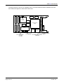
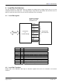
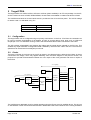
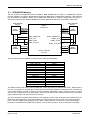
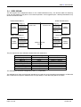
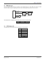
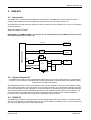
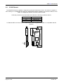
ADM-XRC-II Pro
(ADM-XP)
Hardware Manual
Page 1 of 29
ADM-XR-IIPro User Manual
Version 0.2
Alpha Data
4 West Silvermills Lane
Edinburgh EH3 5BD
UK
Phone:
Fax:
Email:
+44 (0) 131 558 2600
+44 (0) 131 558 2700
[email protected]
Alpha Data
226 Airport Parkway
Suite 470
San Jose
CA 95110
USA
Phone: (408) 467 5076
Fax:
(408) 436 5524
Email: [email protected]
Copyright © 2002, 2003, 2004 Alpha Data Parallel Systems Ltd. All rights reserved.
This publication is protected by Copyright Law, with all rights reserved. No part of this
publication may be reproduced, in any shape or form, without prior written consent from Alpha
Data Parallel Systems Limited.
Page 2 of 29
ADM-XR-IIPro User Manual
Version 0.2
Revision History
Revision
0.1
0.1+
Date
Jul-04
0.2
Nov-04
Page 3 of 29
Comments
Initial
DATA1, DATA8 DATA13 and DATA15 – polarity swapped
DATA38 pin nos swapped in Manual
Clock pins updated for XP pinouts (were XPL pinouts)
Removed XRM-Pro Debug Section – added XRM ETH
ADM-XR-IIPro User Manual
Version 0.2
ADM-XP User Manual
Contents
1
INTRODUCTION .......................................................................................................................................... 5
1.1
2
SPECIFICATIONS ...................................................................................................................................... 5
INSTALLATION ........................................................................................................................................... 6
2.1
2.2
2.3
2.4
MOTHERBOARD REQUIREMENTS ............................................................................................................... 6
HANDLING INSTRUCTIONS ........................................................................................................................ 6
INSTALLING THE ADM-XP ONTO A PMC MOTHERBOARD ........................................................................... 6
INSTALLING THE ADM-XP IF FITTED TO AN ADC-PMC .............................................................................. 6
3
HARDWARE OVERVIEW............................................................................................................................ 7
4
LOCAL BUS ARCHITECTURE ................................................................................................................... 9
4.1
4.2
5
LOCAL BUS SIGNALS ................................................................................................................................ 9
LOCAL BUS TRANSFERS........................................................................................................................... 9
TARGET FPGA.......................................................................................................................................... 10
5.1
5.2
5.3
5.4
5.5
5.6
6
CONFIGURATION .................................................................................................................................... 10
CLOCKS ................................................................................................................................................ 10
SDRAM DDR MEMORY ........................................................................................................................ 12
DDR2 SSRAM..................................................................................................................................... 13
FLASH MEMORY .................................................................................................................................... 14
POWER SUPPLY .................................................................................................................................... 14
FRONT PANEL I/O .................................................................................................................................... 15
6.1
6.2
SAMTEC 180 CONNECTOR - U8 ............................................................................................................. 15
ROCKETIO MULTI-GIGABIT TRANSCEIVERS – U13 .................................................................................. 17
7
USER IO – PMC PN4 (REAR PANEL)...................................................................................................... 18
8
JTAG ACCESS .......................................................................................................................................... 19
8.1
9
JTAG HEADER (J6)............................................................................................................................... 19
XRM-ETH ................................................................................................................................................... 20
9.1
INTRODUCTION ...................................................................................................................................... 20
9.2
GENERAL PURPOSE I/O ......................................................................................................................... 20
9.3
RS232 I/O............................................................................................................................................ 20
9.4
10/100 ETHERNET ................................................................................................................................ 21
9.5
INPUT AND OUTPUT ASSIGNMENTS (ADM-XP)........................................................................................ 22
9.5.1
Mictor I/O...................................................................................................................................... 22
9.5.2
DCI Terminations ......................................................................................................................... 22
9.5.3
Ethernet MAC............................................................................................................................... 23
9.5.4
RS232 .......................................................................................................................................... 23
10
USER I/O XRM IO146 FRONT PANEL VARIANT – REV2.0 ................................................................ 24
11
USER I/O XRM IO146 – ROCKET ......................................................................................................... 27
Page 4 of 29
ADM-XR-IIPro User Manual
Version 0.2
ADM-XP User Manual
1 Introduction
The ADM-XP (XP) is an advanced PCI Mezzanine card (PMC) supporting Xilinx Virtex-II PRO™ (V2PRO)
devices, the latest development in FPGA technology. The XP supports 2VP70, 2VP100 or 2VP125 devices
with two embedded PowerPC processors.
The XP utilises an FPGA PCI bridge developed by Alpha Data supporting 64 bit PCI at up to 66MHz. Future
enhancements will provide compatibility with PCI-X. A high speed multiplexed address and data bus connects
the bridge to the target FPGA.
Memory resources provided on-board include DDR SDRAM, DDR2 SSRAM and flash, all of which are
optimised for direct use by the FPGA using IP and toolkits provided by Xilinx.
Flexible I/O is the key to the ADM-XRC-II series of boards and the XP is compatible with a wide selection of
XRM modules that use the 180 pin Samtec interface.
1.1
Specifications
The ADM-XP supports high performance PCI operation without the need to integrate proprietary cores into the
FPGA.
•
•
•
•
•
•
•
•
•
•
•
Physically conformant to IEEE P1386 Common Mezzanine Card standard
High performance PCI and asynchronous local bus
Local bus speeds of up to 80MHz
Four banks of 256K * 32 bits of DDR2 SSRAM – option for 512K * 32 bits
Two banks of 64MB DDR SDRAM – option for 128MB
Two flash devices of 16MB each for bridge and target devices
User clock programmable between 5MHz and 200MHz
User front panel adapter with up to 146 free IO signals
Supports 3.3V PCI or PCIX at 64 bits
On board 125MHz LVPECL oscillator
8 x RocketIO Multi-Gigabit Transceiver Connections (optional) @ 2.5Gb/s
Page 5 of 29
ADM-XR-IIPro User Manual
Version 0.2
ADM-XP User Manual
2 Installation
This chapter explains how to install the ADM-XP onto a PMC motherboard.
2.1
Motherboard requirements
The XP is a 3.3V only PCI device and is not compatible with systems that use 5V signalling.
The XP must be installed in a PMC motherboard that supplies 3.3V power to the PMC connectors. Ensure that
the motherboard satisfies this requirement before powering it up.
2.2
Handling instructions
Observe precautions for preventing damage to components by electrostatic discharge. Personnel handling the
board should take SSD precautions.
Avoid flexing the board.
2.3
Installing the ADM-XP onto a PMC motherboard
Note: This operation should not be performed while the PMC motherboard is powered up.
The ADM-XP must be secured to the PMC motherboard using M2.5 screws in the four holes provided. The
PMC bezel through which the I/O connector protrudes should be flush with the front panel of the PMC
motherboard.
2.4
Installing the ADM-XP if fitted to an ADC-PMC
The ADM-XP can be supplied for use in standard PC systems fitted to an ADC-PMC carrier board. The ADCPMC can support up to two ADC-PMC cards whilst maintaining host PC PCI compatibility. If you are using a
ADC-PMC64 refer to the supplied documentation for information on jumper settings. With the ADC-PMC64 all
that is required for installation is a 5V or 3V PCI slot that has enough space to accommodate the full-length
card.
It should be noted that the ADC-PMC uses a standard bridge to provide a secondary PCI bus for the ADM-XP
and that some older BIOS code does not set up these devices correctly. Please ensure you have the latest
version of BIOS appropriate for your machine.
Page 6 of 29
ADM-XR-IIPro User Manual
Version 0.2
ADM-XP User Manual
3 Hardware Overview
The XP is based on the architecture of the ADM-XRC-II with changes to accommodate the enhanced
resources and needs of the Virtex-II PRO device.
The XP follows the architecture of the ADM-XRC series and decouples the “target” FPGA from the “bridge”
device to allow the entire target to be available for user applications. This ensures the user can be up and
running with the minimum of effort and without the complexity of PCI design.
The bridge includes local bus control and monitoring together with flexible configuration options for the bridge
and the target device.
The bridge is capable of 66MHz PCI or PCI-X operation with 64-bit or 32-bit operation. The local bus supports
64-bit at upto 80Mhz
The target FPGA is a Virtex-II-PRO device incorporating FPGA fabric, multi-gigabit transceivers and two
PowerPC cores.
DDR SDRAM, ZBT and flash memory connect to the target FPGA and are supported by Xilinx or third party IP.
IO functionality is provided using XRM modules connecting to the 180 pin SAMTEC QSE and 28 pin SAMTEC
QSE DP connectors.
Config
Control
CPLD
Bridge
Config
Flash
Virtex II FG676
2V1500
64/66 PCI
PCIX 133
DDR2
SDRAM
JTAG
Alpha Data PCI/
PCIX to Local Bus
Bridge
SSRAM
SSRAM
IO Connector/
headers
Target
User
Flash
Local Bus
Virtex II Pro - FF1704
2VP70-2VP125
146 Bit
IO Bus
Clocks
MGT Bus
Power
Target
Config
Flash
DDR2
SDRAM
SSRAM
SSRAM
PN4 IO
Page 7 of 29
ADM-XR-IIPro User Manual
Version 0.2
ADM-XP User Manual
The physical layout is shown in the diagram below. The DDR DRAM and DDR2 SSRAM devices are
clam shelled and appear on both sides of the board.
DDR
J
2
J
1
DDR
2V1500
Bridge
Flash
Flash
J
4
J
3
Clock
Gen
2VP70-2VP100
Target
X
R
M
M
E
Z
Z
Power
ZBT
1
JP1 - VIO Selection
1-2 3.3V
2-3 2.5V
Page 8 of 29
1
M
G
T
ZBT
1
J5 - Jtag Header
U13 - Samtec DP Connector
MGT's
U8 - Samtec 180 Connector
(Select IO)
ADM-XR-IIPro User Manual
Version 0.2
ADM-XP User Manual
4 Local Bus Architecture
The XP implements a multi-master local bus between the bridge and the target FPGA using a 32 or 64
multiplexed address and data path. The bridge design is asynchronous and allows the local bus to be run
faster or slower than the PCI bus clock to suit the complexity of the user design.
4.1
Local Bus signals
Signalling Virtex2Pro
default - 2.5V (fast)
LVCMOS/LVTTL
Bank 3
lad[0:63]
lbe_l[0:7]
lads_l
lblast_l
lbterm_l
PCI BUS
Signal
lad[0:63]
lreset_l
lads_l
lblast_l
lbterm_l
lready_l
lclk
lbe_l[0:7]
dreq_l[0:1]
dack_l[0:1]
fhold
fholda
4.2
2V1500 PCI
to
Local Bus Bridge
Type
bidir
unidir
bidir
bidir
bidir
bidir
unidir
bidir
unidir
unidir
unidir
unidir
lready_l
lreset_l
lwrite
ldack_l[1:0]
ldreq_l[1:0]
fholda
fhold
lclk
AC9
AC10
AD9
AD10
AF7
Target FPGA
2VP70/2VP100
AG12
AF2
AF1
AT21
Purpose
Address and data bus.
Reset to target
Indicates address phase
Indicates last word
Indicates ready and requests new address phase
Indicates that target accepts or presents new data
Clock to synchronise bridge and target
Byte qualifiers
DMA request from target to bridge
DMA acknowledge from bridge to target
Target bus request
Bridge bus acknowledge
Local Bus Transfers
Please refer to the ADM-XRC SDK Help for Windows supplied with the XP for information on local bus
transfers.
Page 9 of 29
ADM-XR-IIPro User Manual
Version 0.2
ADM-XP User Manual
5 Target FPGA
The target FPGA is a V2PRO 2VP70, 2VP100 or 2VP125 (when available) in an FF1704 package. On the XP,
all of the resources such as DDR, DDR2 SSRAM, IO and Flash are available no matter what device is fitted.
The V2PRO has 8 banks of I/O and banks 0 and 1 provide the User IO to the front panel . The VCCIO voltage
for banks 0 and 1 is selectable using JP1.
JP1 Link Posn
1-2
2-3
5.1
VCCIO – Front IO
+3V3
+2V5
Configuration
The target FPGA can be configured using two primary mechanisms. In the first, JTAG from the J6 header can
be used to perform downloading of bit-streams as well as remote debug using tools such as GDB and
ChipScope / Pro. The drawback of using JTAG is that a download cable must be connected to the board.
The XP provides a SelectMAP port between the bridge and the target device mapped to the PCI bus. This
enables very rapid download of configuration data controlled by driver and API code in the host. The maximum
speed that can be achieved is 33 Mbytes per second.
5.2
Clocks
There are a number of clock sources in the XP as shown in the diagram below. Although the ICS307 is shown
connected to the bridge, which may appear differently from the block diagram in the previous section, the
purpose is to provide level translation between the 3.3V output of the clock generator and the 2.5V inputs of
the 2VP70.
2.5V signalling
OSC
125MHz
Differential
3.3V signalling
OSC
CLKGEN_CLK1
14.318MHz
ICS307
LCLK
MCLK
CLKGEN_CLK2
Control
PCI 33/66 MHz
2V1500
PCI
Bridge
Bank1 Pair 0S/1P
2VP70
100/125
Virtex
PRO
Bank1 Pair 2S/3P
Bank0 Pair 4S/5P
Bank0 Pair 6S/7P
XRM
Interface
The V2PRO has a dedicated clock for gigabit operation using the Epson 2121CA 125MHz device. This is input
on GCLK4S/5P in bank 5 and should be received in differential LVDS mode. Because of the routing limitations
Page 10 of 29
ADM-XR-IIPro User Manual
Version 0.2
ADM-XP User Manual
within the V2Pro device and the allocation of the MGT resources on the board the MGT’s are currently limited
to 2.5GBps operation using the REFCLK input to the transceivers.
The MCLK signal is input to the FPGA to provide a user clock of between 10 and 200MHz, single ended. The
local bus uses LCLK to synchronize transfers between the bridge and the target and is derived from MCLK by
a divide by 2 in the ICS307. Although the clocks are related, phase is not guaranteed.
A summary of the clock pins is shown in the table below.
Bank
0
0
0
0
1
1
1
1
4
VCCO
JP1 select
JP1 select
JP1 select
JP1 select
JP1 select
JP1 select
JP1 select
JP1 select
2.5V
GCLK
7P
6S
5P
4S
0S
1P
2S
3P
0P
Pin
K22
J22
F22
G22
K21
J21
F21
G21
AT21
Signal
IO_74N_0/GCLK7P
IO_74P_0/GCLK6S
IO_75N_0/GCLK5P
IO_75P_0/GCLK4S
IO_74P_1/GCLK0S
IO_74N_1/GCLK1P
IO_75P_1/GCLK2S
IO_75N_1/GCLK3P
LCLK
4
2.5V
1S
AU21
MCLK
4
4
2
2
2
2
5
5
5
5
2.5V
2.5V
2.5V
2.5V
2.5V
2.5V
2.5V
2.5V
2.5V
2.5V
2P
3S
6P
7S
4P
5S
AP21
AN21
AB12
AA12
AA10
AA9
AU22
AT22
AN22
AP22
DDR2_clk
DDR1_clk
DDR1_clk
DDR1_clkb
DDR2_clk
DDR2_clkb
MGT_clk
MGT_clkb
PN4 fpga_P3
PN4 fpga_N3
Description
User clocks to / from XRM
Local Bus Clock :MCLK divided by 2
User programmable up to
200MHz. Default is 66MHz
Clock feedback DDR DRAM 1
Clock feedback DDR DRAM 0
Used for clock forwarding of
DDR clock outputs
Clock for the MGTs
PN4 IO clocks
If required, XRM related clocks should be terminated on the XRM itself. No terminations are provided on the
XP main board.
Page 11 of 29
ADM-XR-IIPro User Manual
Version 0.2
ADM-XP User Manual
5.3
SDRAM DDR Memory
The XP provides 2 independent banks of 64MB of DDR SDRAM with the option of 128MB when devices
become available. Two Micron MT46V16M16 devices are fitted and are organised as 4Mx16x4. These devices
can be operated at between 75MHz and 133MHz and depending on resource usage within the FPGA, a
2VP70 can easily achieve 100MHz (DDR200) operation. Both banks are driven from Bank2 of the V2Pro.
DDR SDRAM
Bank 0
DDR
SDRAM
DQ0[0:15]
DQS0[0:1]
DQM0[0:1]
Bank 2
VCCO=2.5V
DDR0_AD/BA/CTL
DDR0_CLK
DDR0_CLKB
DDR0_CLK_FB
DDR
SDRAM
DQ0[16:31]
DQS0[2:3]
DQM0[2:3]
DDR SDRAM
Bank 1
DQ1[0:15]
DQS1[0:1]
DQM1[0:1]
DDR
SDRAM
DDR1_AD/BA/CTL
DDR1_CLK
DDR1_CLKB
DDR1_CLK_FB
DQ1[16:31]
DDR
DQS1[2:3] SDRAM
DQM1[2:3]
2VP70 / 2VP100
FF1704
The pins required for the SDRAM controller for each bank are listed below.
Name
DDR_ad[0:12]
DDR_dq[0:31]
DDR_dqs[0:3]
DDR_rasb
DDR_casb
DDR_web
DDR_ba[0:1]
DDR_clk
DDR_clkb
DDR_csb
DDR_cke
DDR_dm[0:1]
DDR_clk_fb
Type
Output
Bidir
Bidir
Output
Output
Output
Output
Output
Output
Output
Output
Output
Input
The DDR controller uses SSTL1 IOB’s for data and control and SSTL1 for address and clocks - Please refer to
the UCF for locations of the DDR pins. Please note that the FPGA requires the Vref pins to be connected for
correct data reception on bank 3 when using SSTL standard. Additionally, bank 4 Vref pins connect to board
Vref but are not required for user applications. These pins should not be configured with pull-up or pull-down
options otherwise the Vref level will be set incorrectly.
The XP is designed to support DDR interface cores supplied by Xilinx using 90 degree phase shifted clocks for
DQS during write operations. This requires DQS pins occupy IOB’s that do not share a clock signal with DQ
pins. In the XP, DQS[0:1] and DQS[2:3] occupy pairs of IOB’s sharing a common clock. Note A trace delay
has been incorporated on the DQS lines of approx 1.5ns to allow the use of local clocking within the FPGA
Page 12 of 29
ADM-XR-IIPro User Manual
Version 0.2
ADM-XP User Manual
5.4
DDR2 SSRAM
The XP supports four independent banks of CIO DDR2 SSRAM memory. The devices fitted are Samsung
512K *36 (K7I163684-FC16) parts or a functional equivalent. As an upgrade option 1Mx36 (K7I323684-FC16)
devices can also be fitted.
DDR2 SSRAM Bank 0
DDR2
SSRAM
Add0[0:21]
Bwe0[0:3]
Cclk0/Cclkb0
Kclk0/Kclkb0
Dq0[0:31]
DDR2 SSRAM Bank 2
Bank 6
VCCO=1.8V
Bank 7
VCCO=1.8V
DDR2 SSRAM Bank1
DDR2
SSRAM
Add1[0:21]
Bwe1[0:3]
Cclk1/Cclkb1
Kclk1/Kclkb1
Dq1[0:31]
Add0[0:21]
Bwe0[0:3]
Cclk0/Cclkb0
Kclk0/Kclkb0
Dq0[0:31]
DDR2
SSRAM
DDR2 SSRAM Bank 3
2VP70 / 2VP100
FF1704
Add0[0:21]
Bwe0[0:3]
Cclk0/Cclkb0
Kclk0/Kclkb0
Dq0[0:31]
DDR2
SSRAM
The pins required for each SSRAM controller bank are listed below.
Name
ZBTx_ad[0:21]
ZBTx_dq[0:31]
ZBTx_rw
ZBTx_bwe{0..3]
ZBTx_nld
ZBTx_Cclk/ZBTx_nCclk
ZBTx_Kclk/ZBTx_nKclk
ZBTx_DOFF
FPGA Pin Type
Output
Bidir
Output
Output
Output
Output
Output
Output
Description
Address bus
Data bus
Read(1) / Write(0)
Byte enables for writes
Initiates a transaction
SSRAM Output Data Clock
SSRAM Clock for Inputs
SSRAM DLL Enable
The SSRAM pins should be configured for HSTL_II_18 operation
The SSRAM clock Cclks and Kclks are intended to be used with clock-forwarding implemented in a DDR IOB
with a DCM used to adjust for SSRAM clock to output delays on the data input path to the FPGA.
Page 13 of 29
ADM-XR-IIPro User Manual
Version 0.2
ADM-XP User Manual
5.5
Flash Memory
The XP supports a flash device connected to the V2PRO for general purpose applications. Typically in
applications that use a PPC core the flash is used to hold bootstrap or application code.
The flash memory has its own set of pins located within banks 3 and 4 of the V2Pro and the IO voltage on the
Flash device is set at 2.5V. It is recommended that the LVCMOS_25 V2Pro IO standard be used for the Flash
Interface.
Bank 3 & 4
VCCO= 2.5V
Flash_adv_n
Flash_wp_n
Flash_cs_n
Flash_we_n
Flash_oe_n
Flash_rst_n
ad[0:23]
dq[0:15]
+2V5
+3V3
VIO
VCC
RC28F256K3
Strataflash K3
Flash_clk
Flash_sts
Flash_wait
2VP70 / 2VP100
FF1704
5.6
A0
Power Supply
The PMC connectors supply +5V and +3V3 to the XP and both of these rails are used with the card.
The +5V rail is used to provide FPGA VIO supplies of 2.5V @ 8A max and 1.8V at 6A max each.
The +3V3 rails is used to provide the FPGA VCC core of 1.5V @ 9A max. These are maximum values for the
individual supply circuits but consideration must be taken to the power envelope that the PMC card is being
deployed
Page 14 of 29
ADM-XR-IIPro User Manual
Version 0.2
ADM-XP User Manual
6 Front Panel I/O
The XP supports standard XRM’s used on the ADM-XRC-II and ADM-XPL cards and also has an additional
connector that brings 7 MGT channels upto the XRM Module site using a differential 28 pin Samtec QSE-DP
series connector to maintain signal integrity.
The XP supports the standard Samtec 180 pin connector but using either with 2.5V or 3.3V signalling which is
globally selected using JP1
JP1 Link Posn
1-2
2-3
6.1
VCCIO – Front IO
+3V3
+2V5
Samtec 180 connector - U8
The table below details the I/O signals that are available on the Samtec 180 connector along with the FPGA
pin that each connects to.
FPGA
Pin
D10
E10
F11
E11
J10
H10
G10
F10
G9
H9
J12
H12
M13
L13
L12
K12
G17
F17
D16
Signal
IO_8N_1
IO_8P_1
IO_19N_1
IO_19P_1
IO_6N_1
IO_6P_1
IO_7N_1
IO_7P_1
IO_1P_1
IO_1N_1
IO_25N_1
IO_25P_1
IO_28N_1
IO_28P_1
IO_21N_1
IO_21P_1
IO_49N_1
IO_49P_1
IO_50P_1
+3V3
+3V3
+3V3
+5V
+5V
Vbatt
+12V
+12V
Presence
TCK
TMS
Connector Pins
1
3
5
7
9
11
13
15
17
19
21
23
25
27
29
31
33
35
37
39
41
43
45
47
49
51
53
55
57
59
2
4
6
8
10
12
14
16
18
20
22
24
26
28
30
32
34
36
38
40
42
44
46
48
50
52
54
56
58
60
Signal
IO_35N_1
IO_35P_1
IO_30P_1
IO_30N_1
IO_58N_1
IO_58P_1
IO_54N_1
IO_54P_1
IO_34P_1
IO_34N_1
IO_2N_1
IO_2P_1
IO_29P_1
IO_29N_1
IO_20P_1
IO_20N_1
IO_26N_1
IO_26P_1
IO_75P_1
IO_75N_1
Serial_ID
Nc
Vref1
+2V5
+2V5
+2V5
-12V
TDI
TRST
TDO
FPGA
Pin
C13
D13
H13
G13
M19
L19
L18
K18
E13
F13
E9
F9
K13
J13
C11
C10
F12
G12
F21
G21
Note 1
Note 1. Vref1 can be provided by the XRM if required and is applied to banks 0 and 1 in common.
Note 2. TCK, TMS, TDI and TDO are connected to the Coolrunner and not the V2PRO.
Page 15 of 29
ADM-XR-IIPro User Manual
Version 0.2
ADM-XP User Manual
(Continued)
FPGA
Pin
D20
C20
K17
L17
J17
H17
H18
G18
E17
E18
K19
J19
H19
G19
K21
J21
E19
F19
G22
F22
H27
G27
J27
K27
D29
E29
K29
L29
BB40
BB41
Signal
IO_73N_1
IO_73P_1
IO_47N_1
IO_47P_1
IO_48N_1
IO_48P_1
IO_55N_1
IO_55P_1
IO_56P_1
IO_56N_1
IO_59N_1
IO_59P_1
IO_60N_1
IO_60P_1
IO_74P_1
IO_74N_1
IO_64P_1
IO_64N_1
IO_75P_0
IO_75N_0
IO_44N_0
IO_44P_0
IO_43N_0
IO_43P_0
IO_85N_0
IO_85P_0
IO_78N_0
IO_78P_0
MGT_SYS_TXP23
MGT_SYS_TXN23
Connector Pins
61
63
65
67
69
71
73
75
77
79
81
83
85
87
89
91
93
95
97
99
101
103
105
107
109
111
113
115
**117
**119
62
64
66
68
70
72
74
76
78
80
82
84
86
88
90
92
94
96
98
100
102
104
106
108
110
112
114
116
**118
**120
Signal
IO_68N_1
IO_68P_1
IO_37N_1
IO_37P_1
IO_38N_1
IO_38P_1
IO_39P_1
IO_39N_1
IO_43N_1
IO_43P_1
IO_44P_1
IO_44N_1
IO_46N_1
IO_46P_1
IO_65N_1
IO_65P_1
IO_37N_0
IO_37P_0
IO_38N_0
IO_38P_0
IO_74P_0
IO_74N_0
IO_39N_0
IO_39P_0
IO_67N_1
IO_67P_1
IO_78N_1
IO_78P_1
MGT_SYS_RXP23
MGT_SYS_RXN23
FPGA
Pin
H20
J20
F15
E15
C15
C14
L16
M16
K16
J16
H16
G16
M17
M18
C19
D19
E28
F28
C29
C28
J22
K22
L27
M27
L20
K20
L14
K14
BB39
BB38
** - Additional MGT channel provided using these pins
FPGA
Pin
K26
L26
L24
M24
E25
E26
H31
J31
G33
F33
E34
F34
H33
J33
C32
C33
H34
G34
E33
D33
C24
D24
E30
F30
K31
L31
F26
G26
E32
F32
Page 16 of 29
Signal
IO_47P_0
IO_47N_0
IO_58N_0
IO_58P_0
IO_56P_0
IO_56N_0
IO_25N_0
IO_25P_0
IO_7P_0
IO_7N_0
IO_2P_0
IO_2N_0
IO_6N_0
IO_6P_0
IO_20P_0
IO_20N_0
IO_1P_0
IO_1N_0
IO_8N_0
IO_8P_0
IO_65P_0
IO_65N_0
IO_34N_0
IO_34P_0
IO_21N_0
IO_21P_0
IO_49N_0
IO_49P_0
IO_19N_0
IO_19P_0
Connector Pins
121
123
125
127
129
131
133
135
137
139
141
143
145
147
149
151
153
155
157
159
161
163
165
167
169
171
173
175
177
179
122
124
126
128
130
132
134
136
138
140
142
144
146
148
150
152
154
156
158
160
162
164
166
168
170
172
174
176
178
180
Signal
IO_35P_0
IO_35N_0
IO_46P_0
IO_46N_0
IO_48P_0
IO_48N_0
IO_59N_0
IO_59P_0
IO_73N_0
IO_73P_0
IO_60N_0
IO_60P_0
IO_29P_0
IO_29N_0
IO_54N_0
IO_54P_0
IO_64N_0
IO_64P_0
IO_67N_0
IO_67P_0
IO_30N_0
IO_30P_0
IO_55N_0
IO_55P_0
IO_26N_0
IO_26P_0
IO_28N_0
IO_28P_0
IO_68N_0
IO_68P_0
FPGA
Pin
C30
D30
M26
M25
J26
H26
J24
K24
C23
D23
G24
H24
K30
J30
K25
L25
E24
F24
K23
L23
G30
H30
G25
H25
G31
F31
L30
M30
J23
H23
ADM-XR-IIPro User Manual
Version 0.2
ADM-XP User Manual
6.2
RocketIO Multi-Gigabit Transceivers – U13
The ADM-XP provides an additional connection upto the XRM module site which provides 7 MGT connection
from the Virtex II pro device. This enables customisable Mulit Gigabit IO capability using XRM modules
interfacing to the additional samtec QSE-DP connector.
Details of the connections to for the XRM MGT signalling is given below :-
FPGA
Pin
A40
A41
A36
A37
BB4
BB5
BB8
BB9
A8
A9
A4
A5
BB36
BB37
Page 17 of 29
Signal
MGT_SYS_TXP2
MGT_SYS_TXN2
MGT_SYS_TXP3
MGT_SYS_TXN3
MGT_SYS_TXP14
MGT_SYS_TXN14
MGT_SYS_TXP15
MGT_SYS_TXN15
MGT_SYS_TXP10
MGT_SYS_TXN10
MGT_SYS_TXP11
MGT_SYS_TXN11
MGT_SYS_TXP22
MGT_SYS_TXN22
Connector Pins
1
3
5
7
9
11
13
15
17
19
21
23
25
27
2
4
6
8
10
12
14
16
18
20
22
24
26
28
Signal
MGT_SYS_RXP2
MGT_SYS_RXN2
MGT_SYS_RXP3
MGT_SYS_RXN3
MGT_SYS_RXP14
MGT_SYS_RXN14
MGT_SYS_RXP15
MGT_SYS_RXN15
MGT_SYS_RXP10
MGT_SYS_RXN10
MGT_SYS_RXP11
MGT_SYS_RXN11
MGT_SYS_RXP22
MGT_SYS_RXN22
FPGA
Pin
A39
A38
A35
A34
BB3
BB2
BB7
BB6
A7
A6
A3
A2
BB35
BB34
ADM-XR-IIPro User Manual
Version 0.2
ADM-XP User Manual
7 User IO – PMC PN4 (rear panel)
User I/O is presented on the User Connector Pn4 via a standard 64-way PMC connector. This should be
routed via a suitable CMC compliant motherboard to an external I/O adapter.
FPGA Pin
AY23
AP23
AN22 (gclk)
AW24
AV24
AT24
AP24
AM24
AV26
AT25
AN25
AU26
AR26
AM26
AL25
AR27
AP27
AM27
AY29
AV28
AW30
AV30
AT30
AP30
AM30
AT31
AR31
AN31
AY33
AV32
AV33
AR33
Page 18 of 29
Signal
REARIO[1]
REARIO[3]
REARIO[5]
REARIO[7]
REARIO[9]
REARIO[11]
REARIO[13]
REARIO[15]
REARIO[17]
REARIO[19]
REARIO[21]
REARIO[23]
REARIO[25]
REARIO[27]
REARIO[29]
REARIO[31]
REARIO[33]
REARIO[35]
REARIO[37]
REARIO[39]
REARIO[41]
REARIO[43]
REARIO[45]
REARIO[47]
REARIO[49]
REARIO[51]
REARIO[53]
REARIO[55]
REARIO[57]
REARIO[59]
REARIO[61]
REARIO[63]
Pn4 Pin
1
3
5
7
9
11
13
15
17
19
21
23
25
27
29
31
33
35
37
39
41
43
45
47
49
51
53
55
57
59
61
63
Pn4 Pin
2
4
6
8
10
12
14
16
18
20
22
24
26
28
30
32
34
36
38
40
42
44
46
48
50
52
54
56
58
60
62
64
Signal
REARIO[0]
REARIO[2]
REARIO[4]
REARIO[6]
REARIO[8]
REARIO[10]
REARIO[12]
REARIO[14]
REARIO[16]
REARIO[18]
REARIO[20]
REARIO[22]
REARIO[24]
REARIO[26]
REARIO[28]
REARIO[30]
REARIO[32]
REARIO[34]
REARIO[36]
REARIO[38]
REARIO[40]
REARIO[42]
REARIO[44]
REARIO[46]
REARIO[48]
REARIO[50]
REARIO[52]
REARIO[54]
REARIO[56]
REARIO[58]
REARIO[60]
REARIO[62]
FPGA Pin
AW23
AR23
AP22(gclk)
AY24
AU24
AR24
AN24
AL24
AV25
AR25
AM25
AT26
AP26
AN26
AL26
AT27
AN27
AL27
AY28
AU28
AY30
AU30
AR30
AN30
AL30
AU31
AP31
AM31
AY32
AU32
AW33
AP33
ADM-XR-IIPro User Manual
Version 0.2
ADM-XP User Manual
8 JTAG Access
The XP provides JTAG access for the fabric of the board through J6. This header will connect to Xilinx
download cables using 3V3 signalling levels and has the following devices present in the scan chain :-
hdr_TDO
hdr_TDI
Target
2VP70/
2VP100
Bridge
2V1500
hdr_TCK
hdr_TMS
tck,tms
The standard XP is configured with the JTAG chain as shown in the table below.
TDI->
8.1
2V1500
2VP70/100
-> TDO
JTAG Header (J6)
The table below shows the pin-out for J5, the primary JTAG connector.
Pin
1
2
3
4
5
6
7
8
9
Page 19 of 29
Function
+3V3
GND
nc
TCK
nc
TDO
TDI
POL
TMS
ADM-XR-IIPro User Manual
Version 0.2
ADM-XP User Manual
9 XRM-ETH
9.1
Introduction
The XRM-ETH is a general-purpose adaptor for the ADM-XPL and ADM-XRC-II series of PMC modules. It
provides 10/100 Ethernet, RS-232 and general purpose I/O for use with a wide variety of IP.
The XRM-ETH is supplied with two cables to enable connections from the XRM-ETH to 15 way PC COM ports
and RJ45 Ethernet.
XRM-ETH-CAB01 for Ethernet
XRM-ETH-CAB02 for RS232
IMPORTANT. The XRM-ETH REV 1 requires the use of 2.5V signalling over the XRM connector and this
should be checked prior to power up.
XRM Connector
LVDS I/O
Mictor-38
Max
3388E
RS232
2x5 hdr
Filter
+3V3
PSU
TX data
+2V5
Magnetics
Infoport
15w
PHY
LEDs
RX data
25MHz
9.2
General Purpose I/O
The XRM-ETH provides 18 pairs of differential-capable I/O plus two single-ended signals on a 38 pin Mictor
connector. This connector is compatible with a wide range of Mictor connectors and is well suited to cabling
systems from Precision Interconnect.
The differential pairs are routed on the XRM-ETH with 100 Ohm impedance and are not terminated to enable
direct routing to the FPGA. The user has the choice of using Virtex DCI or DT termination schemes to provide
the correct termination for each signal pair. For DCI termination the resistor pairs R1/R2 and R4/R5 should be
set to the appropriate value for the desired termination value. By default these resistors are all 100Ohm. The
DT scheme can only be used with some Virtex-II PRO devices and provides a fixed 100R termination for
LVDS and LDT I/O standards without the power requirement of the DCI option.
9.3
RS232 I/O
The XRM-ETH provides two transmit and two receive RS232 signals that can be used for connection to other
XPLs or PC COM ports. The supplied cable connects TX0 and RX0 to a standard 15 pin connector suitable for
use with a PC. Baud rates up to 115K are supported.
Page 20 of 29
ADM-XR-IIPro User Manual
Version 0.2
ADM-XP User Manual
9.4
10/100 Ethernet
The XRM-ETH Ethernet capability is supported by a Kendin KS8721B 2.5V PHY. This device is capable of
auto-sensing 10 or 100Mb networks and has a standard MII interface suitable for connection to MAC IP in the
FPGA. A management interface and reset is also provided.
LEDS are provided on the board and these indicate the following conditions when lit.
D1
D2
D3
D4
Collision
Full Duplex
Speed is 100
Activity
An Ethernet MAC such as the PLB or OPB Ethernet version supplied with EDK6.1i is compatible with this
interface.
J1
5219
J2
Mictor
2
J3
LEDs
J4
Page 21 of 29
MAX
3388E
Pulse
H0013
Samtec-180
KS8721
PHY
ADM-XR-IIPro User Manual
Version 0.2
ADM-XP User Manual
9.5
9.5.1
Input and Output Assignments (ADM-XP)
Mictor I/O
FPGA
Bank
1
1
1
1
1
1
1
1
1
1
1
1
1
1
1
1
1
1
1
1
1
1
1
1
1
1
1
1
1
1
1
1
1
1
1
1
1
1
Pin
E10
D10
D13
C13
E11
F11
H13
G13
H10
J10
L19
M19
F10
G10
K18
L18
C20
D20
F9
E9
L17
K17
C11
C10
J19
K19
G12
F12
G19
H19
M18
M17
K21
J21
F21
G21
F19
E19
XRM-ETH
Samtec
J2 Mictor
3
1
1
3
4
2
2
4
7
5
5
7
6
6
8
8
11
9
9
11
12
10
10
12
15
13
13
15
16
14
14
16
63
17
61
19
24
18
22
20
67
21
65
23
30
22
32
24
83
25
81
27
36
26
34
28
87
29
85
31
88
30
86
32
89
33
91
35
38
34
40
36
95
37
93
38
Signal
PAIR_1_P
PAIR_1_N
PAIR_2_P
PAIR_2_N
PAIR_3_P
PAIR_3_N
PAIR_4_P
PAIR_4_N
PAIR_5_P
PAIR_5_N
PAIR_6_P
PAIR_6_N
PAIR_7_P
PAIR_7_N
PAIR_8_P
PAIR_8_N
PAIR_9_P
PAIR_9_N
PAIR_10_P
PAIR_10_N
PAIR_11_P
PAIR_11_N
PAIR_12_P
PAIR_12_N
PAIR_13_P
PAIR_13_N
PAIR_14_P
PAIR_14_N
PAIR_15_P
PAIR_15_N
PAIR_16_P
PAIR_16_N
CLK2
CLK3
CLK0
CLK1
SINGLE_37
SINGLE_38
9.5.2 DCI Terminations
These pins should be prohibited for place and route. These pins have no other purpose on the XRM-ETH.
FPGA
XRM-ETH
Bank
Pin
Samtec
Value
Signal
0
G27
103
100
VRN_0
0
H27
101
100
VRP_0
1
G9
17
100
VRN_1
1
H9
19
100
VRP_1
Page 22 of 29
ADM-XR-IIPro User Manual
Version 0.2
ADM-XP User Manual
9.5.3 Ethernet MAC
All of these signals use VCCFPIO signalling levels. The VCCO selected by the jumper on the XRC-II/XPL
should match the IOSTANDARD for these pins.
FPGA
Bank
1
1
1
1
1
0
0
1
0
0
0
0
0
0
0
0
1
1
1
1
Pin
H20
G20
F15
E15
C19
G22
F22
D19
E28
F28
C29
C28
J22
K22
L27
K27
E13
F13
K13
J13
Samtec
62
64
66
68
90
97
99
92
94
96
98
100
102
104
106
107
18
20
26
28
XRM-ETH
MAC Signal
RXC
TXC
PD
TXER
RXDV
RXD3
RXD2
RXD1
RXD0
TXEN
TXD0
TXD1
TXD2
TXD3
COL
CRS
MDC
MDIO
RST_N
RXER
Comment
O-ST
O-ST
I
I
O-PD
O-PD
O-PD
O-PD
O-PD
I
I
I
I
I
O-PD
O-PD
I-PU
IO-PU
I-PU
O
Key
I
Input
O
Output
O-PD Output with 2K pulldown
O-ST Output with 25R source resistor
9.5.4
RS232
FPGA
Bank
0
0
0
0
XRM-ETH
Samtec
J4 Header
122
1
124
3
126
7
128
9
Pin
C30
D30
M26
M25
Signal
TX0
RX0
TX1
RX1
The header pin-out is show below.
Signal
GND
GND
POL
GND
GND
Page 23 of 29
Pin
2
4
6
8
10
Samtec
1
3
5
7
9
Signal
TX0
RX0
NC
TX1
RX1
ADM-XR-IIPro User Manual
Version 0.2
ADM-XP User Manual
10 User I/O XRM IO146 Front Panel Variant – Rev2.0
There are 146 I/O signals available on the front panel connector and these can be used individually or in pairs.
All of these pins are compatible with 2.5V and 3.3V signaling (dependant on IO voltage setting on JP1). Care
must be taken when using these signal pins not to exceed the maximum ratings for the V2PRO device.
Each pair of I/O signals is routed as shown below.
FPGA
IO CON
Rt
User[0]
Rs
User[1]
Rs
Rt
User[2]
Rs
User[3]
Rs
The default manufacturing option is Rs=0R and Rt not fitted. Other options are available. Rs can be used to
provide series damping in point to point applications but for LVDS is 0R. Rt is required for LVDS inputs to
provide the termination voltage from the line current.
1
2
151
152
Pin numbering looking into front of XRM IO146 connector
Page 24 of 29
ADM-XR-IIPro User Manual
Version 0.2
ADM-XP User Manual
Pin
Function
1
3
5
7
9
11
13
15
17
19
21
23
25
27
29
31
33
35
37
Data[0] +ve
Data[0] –ve
Data[2] +ve
Data[2] –ve
Data[4] +ve
Data[4] –ve
Data[6] +ve
Data[6] –ve
Data[8] +ve
Data[8] –ve
Data[10]+ve
Data[10] –ve
Data[12]+ve
Data[12] –ve
Data[14]+ve
Data[14] –ve
Single 0
Single 1
+5V fused
Pin
Function
39
41
43
45
47
49
51
53
55
57
59
61
63
65
67
69
71
73
75
Data[16] +ve
Data[16] –ve
Data[18] +ve
Data[18] –ve
Data[20] +ve
Data[20] –ve
Data[22] +ve
Data[22] –ve
Data[24] +ve
Data[24] –ve
Data[26] +ve
Data[26] –ve
Data[28] +ve
Data[28] –ve
Data[30] +ve
Data[30] –ve
Single 3
Single 4
+5V fused
Pin
Function
77
79
81
83
85
87
89
91
93
95
97
99
101
103
105
107
109
111
113
Data[32] +ve
Data[32] –ve
Data[34] +ve
Data[34] –ve
Data[36] +ve
Data[36] –ve
Data[38] +ve
Data[38] –ve
Data[40] +ve
Data[40] –ve
Data[42] +ve
Data[42] –ve
Data[44] +ve
Data[44] –ve
Data[46] +ve
Data[46] –ve
Single 6
Single 7
+5V fused
Page 25 of 29
UCF
name
User[0]
User[1]
User[4]
User[5]
User[8]
User[9]
User[12]
User[13]
User[16]
User[17]
User[20]
User[21]
User[24]
User[25]
User[28]
User[29]
User[34]
User[35]
Term
Res
R1
R3
R5
R7
R9
R11
R14
R16
N/a
N/a
VII Pro
Pin
E10
D10
E11
F11
H10
J10
F10
G10
G9(5)
H9(5)
H12
J12
L13
M13
K12
L12
D16
E19
Pin
Function
2
4
6
8
10
12
14
16
18
20
22
24
26
28
30
32
34
36
38
Data[1] -ve
Data[1] +-ve
Data[3] +ve
Data[3] -ve
Data[5] +ve
Data[5] -ve
Data[7] +ve
Data[7] -ve
Data[9] +ve
Data[9] -ve
Data[11] +ve
Data[11] -ve
Data[13] +ve
Data[13] -ve
Data[15] +ve
Data[15] -ve
Clock[0] +ve
Clock[0] -ve
Single 2
UCF
name
User[40]
User[41]
User[44]
User[45]
User[48]
User[49]
User[52]
User[53]
User[56]
User[57]
User[60]
User[61]
User[64]
User[65]
User[68]
User[69]
User[37]
User[38]
Term
Res
R19
R23
R25
R27
R29
R37
R41
R44
N/a
N/a
VII Pro
Pin
F17
G17
C20
D20
L17
K17
H17
J17
G18
H18
E17
E18
J19
K19
G19
H19
J27
K27
Pin
Function
40
42
44
46
48
50
52
54
56
58
60
62
64
66
68
70
72
74
76
Data[17] +ve
Data[17] -ve
Data[19] +ve
Data[19] -ve
Data[21] +ve
Data[21] -ve
Data[23] +ve
Data[23] -ve
Data[25] +ve
Data[25] -ve
Data[27] +ve
Data[27] -ve
Data[29] +ve
Data[29] -ve
Data[31] +ve
Data[31] -ve
Clock[1] +ve
Clock[1] –ve
Single 5
UCF
name
User[74]
User[75]
User[78]
User[79]
User[82]
User[83]
User[86]
User[87]
User[90]
User[91]
User[94]
User[95]
User[98]
User[99]
User[102]
User[103]
User[108]
User[109]
Term
Res
R48
R50
R52
R54
R56
R58
R60
R62
N/a
N/a
VII Pro
Pin
G27
H27
K26
L26
M24
L24
E26
E25
J31
H31
G33
F33
E34
F34
J33
H33
D19
E28
Pin
Function
78
80
82
84
86
88
90
92
94
96
98
100
102
104
106
108
110
112
114
Data[33] +ve
Data[33] -ve
Data[35] +ve
Data[35] -ve
Data[37] +ve
Data[37] -ve
Data[39] +ve
Data[39] -ve
Data[41] +ve
Data[41] -ve
Data[43] +ve
Data[43] -ve
Data[45] +ve
Data[45] -ve
Data[47] +ve
Data[47] -ve
Clock[2] +ve
Clock[2] -ve
+5V fused
UCF
name
User[2]
User[3]
User[6]
User[7]
User[10]
User[11]
User[14]
User[15]
User[18]
User[19]
User[22]
User[23]
User[26]
User[27]
User[30]
User[31]
User[32]
User[33]
User[36]
UCF
name
User[42]
User[43]
User[46]
User[47]
User[50]
User[51]
User[54]
User[55]
User[58]
User[59]
User[62]
User[63]
User[66]
User[67]
User[70]
User[71]
User[72]
User[73]
User[39]
UCF
name
User[76]
User[77
User[80]
User[81]
User[84]
User[85]
User[88]
User[89]
User[92]
User[93]
User[96]
User[97]
User[100]
User[101]
User[104]
User[105]
User[106]
User[107]
Term
Res
R4
R2
R6
R8
R10
R12
R15
R17
R64
N/a
Term
Res
R20
R22
R24
R26
R28
R30
R38
R42
R67
N/a
Term
Res
R45
R49
R51
R53
R55
R57
R59
R63
R46
-
VII Pro
Pin
H13
G13
D13
C13
L19
M19
K18
L18
E13
F13
F9
E9
K13
J13
C11
C10
F21
G21
C19
VII Pro
Pin
G12
F12
J20
H20
E15
F15
C14
C15
L16
M16
J16
K16
H16
G16
M18
M17
K21
J21
F19
VII Pro
Pin
C28
C29
C30
D30
M26
M25
J26
H26
K24
J24
D23
C23
H24
G24
L25
K25
G22
F22
ADM-XR-IIPro User Manual
Version 0.2
ADM-XP User Manual
Pin
Function
UCF name
115
117
119
121
123
125
127
129
131
133
135
137
139
141
143
145
147
149
151
Data[48] +ve
Data[48] -ve
Data[50] +ve
Data[50] -ve
Data[52] +ve
Data[52] -ve
Data[54] +ve
Data[54] -ve
Data[56] +ve
Data[56] -ve
Data[58] +ve
Data[58] -ve
Data[60] +ve
Data[60] -ve
Data[62] +ve
Data[62] -ve
Single 8
Single 9
+5V fused
User[110]
User[111]
User[114]
User[115]
User[118]
User[119]
User[122]
User[123]
User[126]
User[127]
User[130]
User[131]
User[134]
User[135]
User[138]
User[139]
User[144]
User[145]
1)
2)
3)
4)
5)
Tem
Res
R65
R68
R71
R73
R77
R79
R81
R84
N/a
N/a
VII Pro
Pin
C32
C33
H34(5)
G34(5)
D33
E33
C24
D24
F30
E30
L31
K31
G26
F26
F32
E32
F28
L27
Pin
Function
UCF name
116
118
120
122
124
126
128
130
132
134
136
138
140
142
144
146
148
150
152
Data[49] +ve
Data[49] -ve
Data[51] +ve
Data[51] -ve
Data[53] +ve
Data[53] -ve
Data[55] +ve
Data[55] -ve
Data[57] +ve
Data[57] -ve
Data[59] +ve
Data[59] -ve
Data[61] +ve
Data[61] -ve
Data[63] +ve
Data[63] -ve
Clock[3] +ve
Clock[3] -ve
+5V fused
User[112]
User[113]
User[116]
User[117]
User[120]
User[121]
User[124]
User[125]
User[128]
User[129]
User[132]
User[133]
User[136]
User[137]
User[140]
User[141]
User[142]
User[143]
Tem
Res
R61
R66
R69
R72
R74
R78
R80
R21
R47
-
VII Pro
Pin
K30
J30
F24
E24
L23
K23
H30
G30
H25
G25
F31
G31
M30
L30
H23
J23
J22
K22
Notes
Data[] signals can be used for differential Pairs or single ended signals
Clock[] can be used for differential clocks or single ended clock signals
XRM I0146 connector – AMP/TYCO 767044-4 152 pin Mictor Receptacle
Suggested mating part – AMP/TYCO 1-767007-1 152 pin Mictor Plug or similar
When using the Virtex II Pro DCI these pins are not available for IO
Page 26 of 29
ADM-XR-IIPro User Manual
Version 0.2
ADM-XP User Manual
11 User I/O XRM IO146 – Rocket
The XRM-IO146 - Rocket is based on the XRM-IO146 module but has bank 4 on the mictor used to bring out
the 7 MGT channels available on the ADM-XP boards. The termination scheme on the differential and single
ended IO has also been changed from the standard XRM-IO146 allowing termination for LVPECL and BLVDS
standards to be implemented on the XRM module rather than externally.
FPGA
Rt
User[0]
Rs
User[1]
Rs
User[2]
Rs
User[3]
Rs
IO CON
Rt
The default manufacturing option is Rs=0R and Rt not fitted. Other options are available. Rs can be used to
provide series damping in point to point applications but for LVDS is 0R. Rt is required for LVDS inputs to
provide the termination voltage from the line current.
1
2
LVDS/Select IO
MGT/Rocket IO
151
152
Pin numbering looking into front of XRM IO146 – Rocket connector
Page 27 of 29
ADM-XR-IIPro User Manual
Version 0.2
ADM-XP User Manual
Pin
Function
1
3
5
7
9
11
13
15
17
19
21
23
25
27
29
31
33
35
37
Data[0]+ve
Data[0]–ve
Data[2]+ve
Data[2]–ve
Data[4]+ve
Data[4]–ve
Data[6]+ve
Data[6]–ve
Data[8]-ve
Data[8]+ve
Data[10]+ve
Data[10]–ve
Data[12]+ve
Data[12]–ve
Data[14]+ve
Data[14]–ve
Data[48]+ve
Data[48]-ve
+5V fused
Pin
Function
39
41
43
45
47
49
51
53
55
57
59
61
63
65
67
69
71
73
75
Data[16]+ve
Data[16]–ve
Data[18]+ve
Data[18]–ve
Data[20]+ve
Data[20]–ve
Data[22]+ve
Data[22]–ve
Data[24]+ve
Data[24]–ve
Data[26]+ve
Data[26]–ve
Data[28]+ve
Data[28]–ve
Data[30]+ve
Data[30]–ve
Data[49]+ve
Data[49]-ve
+5V fused
Pin
Function
77
79
81
83
85
87
89
91
93
95
97
99
101
103
105
107
109
111
113
Data[32]+ve
Data[32]–ve
Data[34]+ve
Data[34]–ve
Data[36]+ve
Data[36]–ve
Data[38]+ve
Data[38]–ve
Data[40]+ve
Data[40]–ve
Data[42]+ve
Data[42]–ve
Data[44]+ve
Data[44]–ve
Data[46]+ve
Data[46]–ve
Data[50]+ve
Data[50]-ve
+5V fused
Page 28 of 29
UCF
name
User[0]
User[1]
User[4]
User[5]
User[8]
User[9]
User[12]
User[13]
User[16]
User[17]
User[20]
User[21]
User[24]
User[25]
User[28]
User[29]
User[34]
User[35]
Term
Res
R1
R3
R5
R7
R9
R11
R14
R16
N/a
N/a
VII Pro
Pin
E10
D10
E11
F11
H10
J10
F10
G10
L20
K20
H12
J12
L13
M13
K12
L12
C32
C33
Pin
Function
2
4
6
8
10
12
14
16
18
20
22
24
26
28
30
32
34
36
38
Data[1]-ve
Data[1]+ve
Data[3]+ve
Data[3]-ve
Data[5]+ve
Data[5]-ve
Data[7]+ve
Data[7]-ve
Data[9]+ve
Data[9]-ve
Data[11]+ve
Data[11]-ve
Data[13]-ve
Data[13]+ve
Data[15]-ve
Data[15]+ve
Clock[0]+ve
Clock[0]-ve
Single1
UCF
name
User[40]
User[41]
User[44]
User[45]
User[48]
User[49]
User[52]
User[53]
User[56]
User[57]
User[60]
User[61]
User[64]
User[65]
User[68]
User[69]
User[37]
User[38]
Term
Res
R19
R23
R25
R27
R29
R37
R41
R44
N/a
N/a
VII Pro
Pin
F17
G17
C20
D20
L17
K17
H17
J17
G18
H18
E17
E18
J19
K19
G19
H19
K30
J30
Pin
Function
40
42
44
46
48
50
52
54
56
58
60
62
64
66
68
70
72
74
76
Data[17]+ve
Data[17]-ve
Data[19]+ve
Data[19]-ve
Data[21]+ve
Data[21]-ve
Data[23]+ve
Data[23]-ve
Data[25]+ve
Data[25]-ve
Data[27]+ve
Data[27]-ve
Data[29]+ve
Data[29]-ve
Data[31]+ve
Data[31]-ve
Clock[1]+ve
Clock[1]–ve
Single12
UCF
name
User[74]
User[75]
User[78]
User[79]
User[82]
User[83]
User[86]
User[87]
User[90]
User[91]
User[94]
User[95]
User[98]
User[99]
User[102]
User[103]
User[108]
User[109]
Term
Res
R48
R50
R52
R54
R56
R58
R60
R62
N/a
N/a
VII Pro
Pin
G27
H27
K26
L26
M24
L24
E25
E26
J31
H31
G33
F33
E34
F34
J33
H33
J22
K22
Pin
Function
78
80
82
84
86
88
90
92
94
96
98
100
102
104
106
108
110
112
114
Data[33]+ve
Data[33]-ve
Data[35]+ve
Data[35]-ve
Data[37]+ve
Data[37]-ve
Data[39]+ve
Data[39]-ve
Data[41]+ve
Data[41]-ve
Data[43]+ve
Data[43]-ve
Data[45]+ve
Data[45]-ve
Data[47]+ve
Data[47]-ve
Clock[2]+ve
Clock[2]-ve
+5V fused
UCF
name
User[2]
User[3]
User[6]
User[7]
User[10]
User[11]
User[14]
User[15]
User[18]
User[19]
User[22]
User[23]
User[26]
User[27]
User[30]
User[31]
User[32]
User[33]
User[36]
UCF
name
User[42]
User[43]
User[46]
User[47]
User[50]
User[51]
User[54]
User[55]
User[58]
User[59]
User[62]
User[63]
User[66]
User[67]
User[70]
User[71]
User[72]
User[73]
User[39]
UCF
name
User[76]
User[77
User[80]
User[81]
User[84]
User[85]
User[88]
User[89]
User[92]
User[93]
User[96]
User[97]
User[100]
User[101]
User[104]
User[105]
User[106]
User[107]
Term
Res
R4
R2
R6
R8
R10
R12
R15
R17
R64
N/a
Term
Res
R20
R22
R24
R26
R28
R30
R38
R42
R67
N/a
Term
Res
R45
R49
R51
R53
R55
R57
R59
R63
R46
-
VII Pro
Pin
H13
G13
D13
C13
L19
M19
K18
L18
E13
F13
F9
E9
K13
J13
C11
C10
F21
G21
D16
VII Pro
Pin
G12
F12
J20
H20
E15
F15
C14
C15
L16
M16
J16
K16
H16
G16
M18
M17
K21
J21
E24
VII Pro
Pin
C28
C29
C30
D30
M26
M25
J26
H26
K24
J24
D23
C23
H24
G24
L25
K25
G22
F22
ADM-XR-IIPro User Manual
Version 0.2
ADM-XP User Manual
Pin
Function
UCF name
MGT_SYS_RXP22
MGT_SYS_RXN22
MGT_SYS_RXP11
MGT_SYS_RXN11
Single 5
Single 4
MGT_SYS_RXP10
MGT_SYS_RXN10
MGT_SYS_RXP15
MGT_SYS_RXN15
MGT_SYS_RXP14
MGT_SYS_RXN14
MGT_SYS_RXP3
MGT_SYS_RXN3
MGT_SYS_RXP2
MGT_SYS_RXN2
Single 11
Single 10
Single 9 *
115
117
119
121
123
125
127
129
131
133
135
137
139
141
143
145
147
149
151
1)
2)
3)
4)
Tem
Res
N/a
N/a
N/a
N/a
R71
N/a
N/a
N/a
N/a
N/a
N/a
N/a
N/a
N/a
N/a
N/a
N/a
VII Pro
Pin
BB35
BB34
A3
A2
D19
C19
A7
A6
BB7
BB6
BB3
BB2
A35
A34
A39
A38
M27
L27
Pin
116
118
120
122
124
126
128
130
132
134
136
138
140
142
144
146
148
150
152
Function
UCF name
MGT_SYS_TXP22
MGT_SYS_TXN22
MGT_SYS_TXP11
MGT_SYS_TXN11
Single 7
Single 6
MGT_SYS_TXP10
MGT_SYS_TXN10
MGT_SYS_TXP15
MGT_SYS_TXN15
MGT_SYS_TXP14
MGT_SYS_TXN14
MGT_SYS_TXP3
MGT_SYS_TXN3
MGT_SYS_TXP2
MGT_SYS_TXN2
Single 2
Single 3
Single 8 *
Tem
Res
N/a
N/a
N/a
N/a
R69
N/a
N/a
N/a
N/a
N/a
N/a
N/a
N/a
N/a
N/a
R47
-
VII Pro
Pin
BB36
BB37
A4
A5
F28
E28
A8
A9
BB8
BB9
BB4
BB5
A36
A37
A40
A41
E19
F19
Notes
Data[] signals can be used for differential Pairs or single ended signals
Clock[] can be used for differential clocks or single ended clock signals
XRM I0146 connector – AMP/TYCO 767044-4 152 pin Mictor Receptacle
Suggested mating part – AMP/TYCO 1-767007-1 152 pin Mictor Plug or similar
Page 29 of 29
ADM-XR-IIPro User Manual
Version 0.2