1
Platform Developer’s Kit
RC10 Manual
RC10 Manual
Conventions
The following conventions are used in this document.
2
Warning Message. These messages warn you that actions may damage your hardware.
Ï
Handy Note. These messages draw your attention to crucial pieces of information.
Hexadecimal numbers will appear throughout this document. The convention used is that of prefixing
the number with '0x' in common with standard C syntax.
Sections of code or commands that you must type are given in typewriter font like this:
void main();
Information about a type of object you must specify is given in italics like this:
copy SourceFileName DestinationFileName
Optional elements are enclosed in square brackets like this:
struct [type_Name]
Curly brackets around an element show that it is optional but it may be repeated any number of times.
string ::= "{character}"
Page 2
www.celoxica.com
RC10 Manual
Assumptions & Omissions
This manual assumes that you:
•
have used Handel-C or have the Handel-C Language Reference Manual
•
are familiar with common programming terms (e.g. functions)
•
are familiar with your operating system (Linux or MS Windows)
This manual does not include:
•
instruction in VHDL or Verilog
•
instruction in the use of place and route tools
•
tutorial example programs. These are provided in the Handel-C User Manual
Page 3
www.celoxica.com
RC10 Manual
Contents
1 RC10 OVERVIEW ........................................................................................................ 8
2 RC10 GETTING STARTED .......................................................................................... 10
2.1 RC10: SYSTEM REQUIREMENTS ........................................................................... 10
2.2 RC10: UNPACKING THE BOARD ........................................................................... 10
2.3 RC10: CONNECTING THE CABLES ........................................................................ 10
2.4 RC10: SWITCHING ON THE POWER ....................................................................... 10
2.5 RC10: INSTALLING DRIVERS ................................................................................ 10
2.6 RC10: RUNNING THE INSTALLED DEMOS .............................................................. 11
2.7 RC10: BUILDING THE PROVIDED EXAMPLES .......................................................... 11
2.8 RC10: DOWNLOADING DESIGNS TO THE BOARD .................................................... 12
2.9 RC10: CREATING FPGA CONFIGURATION FILES ................................................... 13
2.10 RC10: PROJECT IDEAS ..................................................................................... 14
3 RC10 HARDWARE DESCRIPTION ................................................................................ 17
3.1 RC10: OVERVIEW OF DEVICES AND CONNECTORS ................................................. 17
3.2 RC10: FPGA .................................................................................................... 18
3.3 RC10: CLOCKS .................................................................................................. 19
3.4 RC10: LEDS ..................................................................................................... 19
3.5 RC10: SEVEN SEGMENT DISPLAYS...................................................................... 19
3.6 RC10: JOYSTICK ................................................................................................ 20
3.7 RC10: PS/2 PORT FOR MOUSE AND KEYBOARD .................................................... 21
3.8 RC10: RS232 SERIAL PORT ............................................................................... 21
3.9 RC10: ANALOGUE TO DIGITAL CONVERTERS ....................................................... 21
3.10 RC10: VIDEO OUTPUTS .................................................................................... 22
3.11 RC10: CAMERA ............................................................................................... 22
3.12 RC10: AUDIO ................................................................................................... 23
3.13 RC10: USB MICROCONTROLLER ...................................................................... 23
3.14 RC10: FLASH MEMORY .................................................................................... 24
3.15 RC10: CAN INTERFACE .................................................................................... 24
3.16 RC10: SERVO MOTOR INTERFACE ...................................................................... 24
3.17 RC10: 50-PIN EXPANSION HEADER ................................................................... 24
3.18 RC10: RESET BUTTON ...................................................................................... 27
3.19 RC10: JTAG CONNECTION ............................................................................... 27
3.20 RC10: EXTERNAL POWER CONNECTOR ............................................................. 27
3.21 RC10: DATASHEETS AND DEVICE SPECIFICATIONS ............................................. 27
3.22 RC10: SCHEMATICS ......................................................................................... 28
4 RC10 PLATFORM SUPPORT LIBRARY (PSL)............................................................... 29
4.1 RC10 PSL: CLOCKS .......................................................................................... 29
4.1.1 Selecting a specific clock ...................................................................................................... 29
4.1.2 Selecting clocks automatically............................................................................................... 29
4.2 RC10 PSL: LEDS.............................................................................................. 30
4.2.1 Writing to LEDs by index ....................................................................................................... 30
4.2.2 Writing to all LEDs................................................................................................................. 30
4.2.3 Writing to a specific LED ....................................................................................................... 30
4.3 RC10 PSL: SEVEN SEGMENT DISPLAYS .............................................................. 31
Page 5
www.celoxica.com
RC10 Manual
4.3.1 Writing shapes to seven segment displays ........................................................................... 31
4.3.2 Writing digits to seven segment displays .............................................................................. 31
4.4 RC10 PSL: JOYSTICK ........................................................................................ 32
4.4.1 Reading buttons by index...................................................................................................... 32
4.4.2 Reading all buttons................................................................................................................ 32
4.4.3 Reading a specific button ...................................................................................................... 32
4.5 RC10 PSL: PS/2 PORT ...................................................................................... 33
4.5.1 Running the PS/2 ports ......................................................................................................... 33
4.5.2 Reading from the PS/2 ports ................................................................................................. 33
4.5.3 Writing to the PS/2 ports ....................................................................................................... 33
4.6 RC10 PSL: RS232 SERIAL PORT ....................................................................... 34
4.6.1 Running the RS232 port........................................................................................................ 34
4.6.2 Changing the baud rate......................................................................................................... 35
4.6.3 Changing the parity setting.................................................................................................... 36
4.6.4 Changing the flow control...................................................................................................... 36
4.6.5 Reading from the RS232 port................................................................................................ 36
4.6.6 Writing to the RS232 port ...................................................................................................... 36
4.7 RC10 PSL: ANALOGUE TO DIGITAL CONVERTORS ............................................... 37
4.7.1 Running the ADCs................................................................................................................. 37
4.7.2 Setting the ADC range .......................................................................................................... 37
4.7.3 Setting the ADC offset........................................................................................................... 38
4.7.4 Reading from the ADCs ........................................................................................................ 38
4.8 RC10 PSL: VIDEO OUTPUT ................................................................................ 38
4.8.1 Running the video output ...................................................................................................... 38
4.8.2 Querying video mode properties ........................................................................................... 40
4.8.3 Changing the video mode ..................................................................................................... 40
4.8.4 Generating video output pixels.............................................................................................. 40
4.8.5 Finding the current video output position .............................................................................. 41
4.8.6 Finding the current video output blanking state .................................................................... 41
4.8.7 Finding the current video output sync state .......................................................................... 41
4.9 RC10 PSL: CAMERA .......................................................................................... 41
4.9.1 Running the camera .............................................................................................................. 41
4.9.2 Setting the camera mode ...................................................................................................... 43
4.9.3 Reading pixels from the camera............................................................................................ 43
4.10 RC10 PSL: AUDIO OUTPUT .............................................................................. 44
4.10.1 Running the audio interface ................................................................................................ 44
4.10.2 Setting the audio sample rate.............................................................................................. 44
4.10.3 Writing stereo samples to the audio output......................................................................... 45
4.11 RC10 PSL: BUZZER......................................................................................... 45
4.12 RC10 PSL: MICROCONTROLLER INTERFACE (FOR USB AND FLASH) ................... 46
4.12.1 Running the microcontroller interface ................................................................................. 46
4.13 RC10 PSL: CAN INTERFACE ............................................................................ 46
4.14 RC10 PSL: SERVO MOTOR INTERFACE .............................................................. 46
4.14.1 Running the servo motors ................................................................................................... 46
4.14.2 Controlling the servo motors ............................................................................................... 47
4.15 RC10 PSL: USB DATA .................................................................................... 47
4.15.1 Writing data to the host over USB....................................................................................... 47
4.15.2 Reading data from the host over USB ................................................................................ 48
4.16 RC10 PSL: FLASH RAM.................................................................................. 48
4.16.1 Writing to Flash ................................................................................................................... 48
4.16.2 Reading from Flash ............................................................................................................. 49
4.16.3 Formatting the Flash ........................................................................................................... 49
4.16.4 Erasing files from Flash....................................................................................................... 49
4.16.5 Finding the length of files in Flash....................................................................................... 50
4.16.6 Reconfiguring the FPGA from Flash ................................................................................... 50
4.17 RC10 PSL: EXPANSION HEADER ...................................................................... 50
Page 6
www.celoxica.com
RC10 Manual
4.17.1 Running the expansion port ................................................................................................ 50
4.17.2 Setting the state of expansion pins ..................................................................................... 51
4.17.3 Reading the state of expansion pins ................................................................................... 52
5 RC10 PLATFORM ABSTRACTION LAYER ..................................................................... 54
5.1 RC10 PAL: CLOCKS .......................................................................................... 54
5.2 RC10 PAL: LEDS ............................................................................................. 54
5.3 RC10 PAL: SEVEN SEGMENT DISPLAYS.............................................................. 55
5.4 RC10 PAL: JOYSTICK ........................................................................................ 55
5.5 RC10 PAL: PS/2 PORT ...................................................................................... 55
5.6 RC10 PAL: RS232 SERIAL PORT ....................................................................... 55
5.7 RC10 PAL: ANALOGUE TO DIGITAL CONVERTORS ............................................... 55
5.8 RC10 PAL: VIDEO OUTPUT ................................................................................ 56
5.9 RC10 PAL: CAMERA ......................................................................................... 56
5.10 RC10 PAL: AUDIO OUTPUT .............................................................................. 56
5.11 RC10 PAL: CAN INTERFACE ........................................................................... 57
5.12 RC10 PAL: SERVO MOTOR INTERFACE .............................................................. 57
5.13 RC10 PAL: USB DATA .................................................................................... 57
5.14 RC10 PAL: FLASH RAM.................................................................................. 57
6 INDEX ....................................................................................................................... 59
Page 7
www.celoxica.com
RC10 Overview
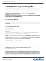
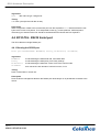
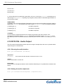
1 RC10 Overview
RC10 BLOCK DIAGRAM
•
Xilinx Spartan 3L XC3S1500L-4-FG320
•
5-way micro joystick
•
PS/2 port for mouse and keyboard
•
RS-232 serial port
•
2 analogue to digital converters
•
VGA output
•
optional LCD video output
•
audio output (stereo PWM, and piezo transducer)
•
USB Microcontroller for:
•
• USB 2.0 port management
• FPGA configuration/reconfiguration
• Flash memory management
2 seven-segment displays
•
8 green LEDs
•
50 pin expansion header including:
•
• 33 general I/O pins
• 3 power pins (+12V, +5V, +3.3V)
• 2 clock pins
Servo motor connector to drive up to 4 motors.
•
CAN bus connector
Page 8
www.celoxica.com
RC10 Overview
•
JTAG connector
•
Celoxica Platform Developer's Kit including:
•
•
•
Platform Support Library for RC10
Platform Abstraction Layer for RC10
FTU3 file transfer utility (for Windows 2000 and Windows XP)
Page 9
www.celoxica.com
RC10 Overview
2 RC10 Getting started
This section describes how to set up and start using your RC10.
2.1 RC10: System requirements
Using the Celoxica RC10 requires the following:
•
DK Design Suite. Only required if you want to use the RC10 PAL and PSL libraries.
•
Microsoft Windows 2000 or Windows XP for the FTU3 program and for use of the DK
Design Suite.
•
Microsoft Visual Studio .NET in order to write applications on the host PC that interface with
the RC10.
2.2 RC10: Unpacking the board
You should take care to avoid static discharge when handling the RC10 board, as this may damage it.
You are recommended to use an earth strap. If an earth strap is not available, ensure that you make
contact with earth before and during handling of the board, and only handle the board by its edges.
2.3 RC10: Connecting the cables
The board must be powered down before you attach cables. The connectors are labelled on the board
and in the overview of devices and connectors.
You will need to connect the board to your PC with a standard USB cable if you want to use the Celoxica
FTU3 program to download FPGA configuration files, or to read from or write to Flash memory.
2.4 RC10: Switching on the power
The RC10 board can draw power from the host PC via the USB cable, or an optional external power
supply can be connected to connector CN18, which is of the type commonly used for PC hard disk
drives and CD/DVD drives.
Note that if you wish to use the servo motor connector (CN9), the 5V supplies on the ATA connector
(CN13) or the optional LCD panel with a backlight then an external power supply must be connected.
Peripheral devices should be connected before the RC10 board is turned on. Otherwise the devices
may not function correctly.
When turned on the 'Power' LED (D14) should illuminate.
2.5 RC10: Installing drivers
When the RC10 is plugged into a PC running Windows XP or 2000, the operating system will ask for
driver files to be supplied. These are installed by the PDK installer into the
PDKInstallDir\Software\Drivers\RCUSB directory. Once these are installed, the board is ready
for use. Running the FTU3 application will then allow you to access the board.
Page 10
www.celoxica.com
RC10 Overview
2.6 RC10: Running the installed demos
Once the RC10 has been installed and plugged into a PC, it will boot into its "Intro" screen. From here,
you can use the on-board joystick to navigate through a list of pre-installed demos. Pressing the centre
button of the joystick will configure the device with the selected demo. Press the reset button (adjacent
to the USB cable) to return to the intro screen.
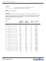
2.7 RC10: Building the provided examples
There are three workspaces containing examples relevant to the RC10.
PAL Examples Workspace
The PAL Examples Workspace can be launched from Start>Programs>Celoxica>Platform Developer's
Kit>PAL>PAL Examples Workspace. The following examples will build for the RC10:
Example
Description
DumbTerminal
A "dumb terminal" program for connecting to RS232 peripherals. Characters
typed on the keyboard are sent to the RS232 port. Characters received on
the RS232 port are displayed on the VGA output. RS232 port is configured
as 115200 baud, 8N1.
Console
A simple demonstration of PAL Console, an easy way of display text on the
VGA output.
FrameBufferBRAM
A demonstration of PAL FrameBufferBRAM, a low resolution
BlockRAM-based framebuffer.
Keyboard
Echo characters typed on the keyboard to the VGA output. Keyboard must
be plugged into the PS/2 port via a mouse/keyboard splitter.
LED
A simple LED flasher.
Life
Highly parallel game-of-life implementation. Computes over 65 billion cell
iterations per second.
Mouse
A demonstration of mouse input. Attach a mouse to the PS/2 port, and a
coloured block can be moved around the screen.
PalTest
Generic PAL test program.
Player
A demonstration of USB data transfers and audio output. WAV files sent to
the USB port by the host PC will be played via the audio out jack. Send the
files with a command line such as "rcx -uw myfile.wav".
SevenSeg
A simple 7-segment display test program.
VideoOut
A simple video display program, displays a static XOR pattern on the VGA
output.
PSL Examples Workspace
The PSL Examples Workspace can be launched from Start>Programs>Celoxica>Platform Developer's
Kit>PSL>RC10>Examples Workspace [DK]. This workspace contains the following examples:
Page 11
www.celoxica.com
RC10 Overview
Example
Description
ADC
Oscilloscope program, demonstrating the use of the high-speed
analog-to-digital converters (ADCs).
Camera
Camera test program. Requires an OV9650 to be fitted to the CMOS
camera socket.
Expansion
Logic analyser program, demonstrating simple use of the expansion port.
FlashUSB
Demonstration of FX2 microcontoller interface, providing access to the
Flash storage and USB data transfers. Should be used in conjuction with the
software FlashUSB test program, accessible from
Start>Programs>Celoxica>Platform Developer's Kit>PSL>RC10>Examples
Workspace [VC++].
MidiFlash
Plays polyphonic melodies from files in flash created with the provided
application, mid2flash. First melody played is in flash index 200.
Demonstrates use of audio out and flash access.
Servo
Sweeps each of the four servos through a sine wave.
PixelStreams Examples Workspace
The PixelStreams Examples Workspace can be launched from Start>Programs>Celoxica>Platform
Developer's Kit>PixelStreams>Examples Workspace [DK]).
The following examples will build for the RC10: BRAMBuffer, BusMap, Camera, Console,
CustomCoord, Dither, GUI, Noise, Pong, PortIO, Rotate, SyncGenDynamic, TestCard, VideoGen.
Please consult the PixelStreams Manual for more information about these examples.
Building the examples
To build any of the examples, do the following:
1. Open the relevant workspace within DK, or from the Start menu.
2. Right-click on project and click on select Set as Active Project.
3. Select "RC10" from the drop-down configurations menu on the toolbar.
4. Press F7 to start the build.
The example will be automatically compiled, placed and routed, resulting in a ".bit" file.
2.8 RC10: Downloading designs to the board
To download newly built designs to the board:
1. Open FTU3 from the Start menu (Start>Programs>Celoxica>Platform Developer's Kit>FTU3).
2. The RC10 should be shown in the list of attached boards. Double-click it.
3. Click the FPGA tab, select Browse, and navigate to the location of your new bit file. For
example, InstallDir\PDK\Examples\PAL\LED\RC10 for the PAL LED example.
4. Double-click the bit file (for example, LED.bit).
5. Click Configure. The FPGA will immediately be reconfigured (it takes only a matter of
milliseconds).
FTU3 can also be used to program the Flash on the board.
You can also access the board from the command line using the rcx utility. For example: rcx -c
InstallDir\PDK\Examples\PAL\LED\RC10\LED.bit will configure the first attached board with
the given bit file. Consult the RC host library and FTU3 manual for more information.
Page 12
www.celoxica.com
RC10 Overview
2.9 RC10: Creating FPGA configuration files
There are several simple steps to creating FPGA configuration files for the RC10 using DK and PDK.
Please see the DK manual for more information on these steps.
Setting up DK
You must set up your DK project to use the correct FPGA, using the Linker tab in the Project Settings:
•
set device to "xc3s1500l"
•
set package to "fg320"
•
set speed to "4"
If you would like DK to call the Xilinx ISE Place and Route tools to complete production of the FPGA
configuration file after the build to EDIF is complete, then you need to add two post-build steps to the
Build Commands tab in the DK Project Settings. The build commands should look like this:
cd $(TargetDir)
edifmake_rc10.bat $(TargetName)
and the "Output" must be set to:
$(TargetDir)\$(TargetName).bit
Using the edifmake_rc10 batch file
If you choose not to have DK automatically run the Xilinx ISE Place and Route tools, you can run them
yourself from the command line using a batch file provided by Celoxica, as follows:
•
open a DOS command prompt, and change to the DK output directory for your project (e.g.
EDIF, or RC10)
•
type "edifmake_rc10 <ProjectName>" where ProjectName is the name of the EDIF
file generated for your project. Do not include the ".edf" extension in ProjectName, e.g.
to build MyDesign.edf you would type "edifmake_rc10 MyDesign".
Performing Place and Route manually
If you do not wish to use the edifmake_rc10 batch file, either within DK or at the command-line, then
it is possible to manually create a project in Xilinx ISE to place and route your design. For further
information on this please consult the manuals for your Xilinx ISE software. If you take this route, then be
sure to note the following settings you must make for bitgen, either at the command line or in the ISE
GUI:
Property
Setting
LCK_cycle
5
Match_cycle
Auto
DONE_cycle
6
GTS_cycle
4
GWE_cycle
Done
DonePin
PullUp
M0Pin
PullDown
M1Pin
PullUp
Page 13
www.celoxica.com
RC10 Overview
M2Pin
PullUp
CclkPin
PullNone
ProgPin
PullNone
DriveDone
Yes
2.10 RC10: Project ideas
Here are a few project ideas for using an RC10. Celoxica makes no claims as to the difficulty or
feasibility of these projects (although we believe them to be possible), they are merely suggestions to
stimulate the imagination.
Robotics
•
Audio
Animatronic eyes (e.g. see http://www.androidworld.com/prod31.htm
http://www.androidworld.com/prod31.htm)
•
Autonomous hovercraft
•
Autonomous helicopter
•
Autonomous tank
•
MIDI jukebox
•
MP3 jukebox
•
MOD tracker
•
Speech synthesiser
•
Speech recogniser
•
Analogue synth (e.g. Moog) emulator
Video demos
• 3D scan-line rasteriser
•
3D wireframe renderer
•
GUI system
•
Light cycles
•
Defender
•
Asteroids
•
Mario Kart style racer
•
Multiplayer games (via RS232)
Games
Video processing (need camera)
• Webcam
•
Object tracking
•
Face tracking
Page 14
www.celoxica.com
RC10 Overview
•
Barcode reader
•
Mini camcorder
Microprocessors
• Microblaze
•
CPUs from OpenCores.org
•
Design your own CPU
Signal processing
• Oscilloscope with more features
•
Logic analyser
•
Spectrum analyser (real-time FFT)
•
Simulink integration via USB
•
LabView integration via USB
•
Composite / S-Video input (via ADCs)
•
Radio receiver (sampling 10.7MHz intermediate frequency of FM radio)
•
Teletext decoder
Emulators
• VIC 20
•
ZX Spectrum
•
BBC Micro
•
Atari 2600
•
Apple IIe
•
PDP-10
•
Arcade machines (e.g Space Invaders, PacMan)
Virtual Peripherals
• Use host program to bridge USB to Ethernet, then implement TCP/IP, Webserver, etc
•
Use host program to bridge USB to video, e.g. webcam to PixelStreams to PC display
Cryptography / Compression / Error Correction
• DES cracker
•
Rijndael encrypt / decrypt accelerator
•
Elliptic curve cryptography
•
GZIP compression / decompression
•
Viterbi error correction
•
TurboCode error correction
•
LDPC error correction
Cellular automata
• Game of life
•
Lattice gas simulation
Page 15
www.celoxica.com
RC10 Overview
Other
•
Engine diagnostics/management unit
•
Hard disk interface (data logger, video recording)
Page 16
www.celoxica.com
RC10 Getting started
3 RC10 Hardware Description
This section details the devices that comprise the RC10 board.
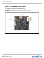
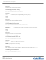
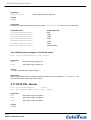
3.1 RC10: Overview of devices and connectors
RC10 DEVICES
Page 17
www.celoxica.com
RC10 Getting started
RC10 CONNECTORS
3.2 RC10: FPGA
The RC10 board has a Xilinx Spartan 3 XC3S1500L-4-FG320. The device has direct connections to the
following devices:
•
USB Microcontroller
•
Video output
•
Audio output
•
RS-232 port
•
PS/2 connector
•
Expansion header
•
CAN bus connector
•
Servo motor connector
•
Analogue to Digital convertors
•
8 green LEDs
•
2 seven segment LED displays
•
5-way micro joystick
•
TFT flat screen (if fitted)
Details of pin connections are given in the sections about these devices.
Page 18
www.celoxica.com
RC10 Getting started
Ï
If you are programming the board using Handel-C, remember that the pins should be listed
in MSBit to LSBit order.
The FPGA also has access to Flash memory through the USB microcontroller.
You can program the FPGA using the microcontroller from the Flash memory, or from the USB.
3.3 RC10: Clocks
The RC10 provides one fixed clock and two external clock inputs to the FPGA. These are connected as
follows:
Function
Fixed clock 48.000 MHz
FPGA Pin
P10
Expansion clock 0
E10
Expansion clock 1
F10
3.4 RC10: LEDs
The RC10 has eight green LEDs that can be directly controlled from the FPGA. The LEDs are numbered
right-to-left (so the rightmost LED on the board is bit 0) to simplify reading binary values. They are
connected as follows:
LED pins
FPGA Pins
LED0
D2
LED1
D3
LED2
E1
LED3
E2
LED4
E3
LED5
F2
LED6
F4
LED7
The board also has two other LEDs:
G3
•
D14 (Power)
•
D13 (FPGA Configuration Done)
3.5 RC10: Seven Segment Displays
The RC10 has two Seven Segment LED displays.
Page 19
www.celoxica.com
RC10 Getting started
Description
FPGA Pins
Seven Segment 0 'a'
H2
Seven Segment 0 'b'
H3
Seven Segment 0 'c'
H6
Seven Segment 0 'd'
H5
Seven Segment 0 'e'
G5
Seven Segment 0 'f'
G4
Seven Segment 0 'g'
H1
Seven Segment 0 'dp'
C2
Seven Segment 1 'a'
J1
Seven Segment 1 'b'
J2
Seven Segment 1 'c'
K2
Seven Segment 1 'd'
C3
Seven Segment 1 'e'
C1
Seven Segment 1 'f'
H4
Seven Segment 1 'g'
B1
Seven Segment 1 'dp'
J4
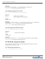
The segments of the display are labelled "a-g" and "dp" in the table above and the figure below.
LAYOUT OF SEVEN SEGMENT DISPLAY
3.6 RC10: Joystick
There are five contacts under the joystick, one in the centre and one each for left, right, up and down.
When pressed, these act as momentary high inputs into the FPGA.
Description
FPGA Pins
Left
A10
Right
D10
up
B13
Down
A11
Select/Fire
B10
Page 20
www.celoxica.com
RC10 Getting started
3.7 RC10: PS/2 port for mouse and keyboard
The RC10 board has a PS/2 port on the PCB which can be used with a mouse/keyboard cable splitter.
The DATA and CLK lines of this port are mapped directly through to the FPGA. The board supplies +5V
to power the devices, but they should not use more than 100mA.
PS/2 pins
Description
FPGA pins
KM0
Mouse DATA
R10
KM1
Mouse CLK
V11
KM2
Keyboard DATA
V12
KM3
Keyboard CLK
R13
3.8 RC10: RS232 Serial port
The RC10 board has one RS-232 port, implemented via a Intersil ICL3222ECA RS-232 transceiver. The
pins on the RS-232 port are:
Description
Function
FPGA pins
PortCTS
CTS (Clear To Send)
T5
PortRxData
RxD (Receive data)
T4
PortRTS
RTS (Request To Send)
R5
PortTxData
TxD (Transmit data)
U5
3.9 RC10: Analogue to Digital Converters
The RC10 has two analogue to digital converters, based on the National Semiconductor ADC10065,
and with a BNC socket for the analogue input. Each ADC channel has its own set of pins on the FPGA,
and there is one shared pin which must be driven high to enable the power supply for the ADCs.
Page 21
www.celoxica.com
RC10 Getting started
Description
FPGA Pins
ADC0 data
K1, L4, L3, L2, L1, M4, M3, N4, N2, P4
ADC0 Trigger
N5
ADC0 DC Offset (PWM)
U18
ADC0 Standby
T18
ADC0 IRS
L6
ADC0 Clock
M5
ADC1 data
U1, T1, T2, T3, R1, R2, R3, P1, P2, P3
ADC1 Trigger
M1
ADC1 DC Offset (PWM)
P16
ADC1 Standby
R16
ADC1 IRS
K4
ADC1 Clock
L5
NotShutdown - both ADCs
R17
3.10 RC10: Video Outputs
The RC10 has two video output capabilities: VGA and LCD. At present a LCD screen is not shipped with
the RC10, so the data included here for the LCD output is for information only.
VGA output
Description
FPGA Pins
Red component data pins
D5, A4, B4, C4, A3, B3, A2
Green component data pins
C7, D7, B6, D6, A5, B5, C5
Blue component data pins
A9, B9, D9, F9, E9, E7, A7
HSync pin
P7
VSync pin
P6
DDC Data pin
P8
DDC Clock pin
R9
LCD output
Description
FPGA Pins
LCD data pins
H13, H14, J15, J14, F14, G14, H16, H15
LCD Enable pin
J18
3.11 RC10: Camera
The RC10 has a connector for a CMOS camera, the OmniVision OV9650. The pin numbers are as
shown below:
Page 22
www.celoxica.com
RC10 Getting started
Description
FPGA Pins
Reset
P18
Power Down
R18
SCCB serial data
K14
SCCB serial clock
K13
VSYNC
K15
HREF
K17
Cystal clock input
K18
Clock output
N10
Data [9 to 0]
L15, L16, L18, L17, M16, N17, M15, P17, N15, P15
3.12 RC10: Audio
The RC10 has two audio outputs:
•
Stereo PWM output with an RC network for smoothing and a decoupling capacitor.
•
Piezo buzzer
The pins for the stereo PWM output are:
Description
FPGA Pins
Left Channel
U4
Right Channel
The pins for the piezo buzzer are:
V5
Description
FPGA Pins
Pin 0
U6
Pin 1
V7
3.13 RC10: USB Microcontroller
The RC10 includes a Cypress CY7C68013-56pvc FX2 microcontroller which manages interaction
between the USB port connected to the host computer, the Flash memory and the FPGA.
FPGA connections to the microcontroller are:
Function
FPGA Pins
Data Bus[7:0]
U13, T11, P12, R11, T8, V8, R8, R6
Chip Select (GPIF0)
T14
Write Enable
V4
FIFO Full
R14
Page 23
www.celoxica.com
RC10 Getting started
FIFO Empty
P14
GPIF 1
V10
GPIF 2
P13
GPIF 3
N8
The FPGA can access both the NAND Flash and I2C bus by sending commands via the GPIF interface.
The FX2 processor implements a basic filesystem containing numbered files starting from file 1 and up
to file 254. The file numbers do not need to be contiguous.
3.14 RC10: Flash Memory
The RC10 is provided with a 16-MB Flash RAM. The Flash is only accessible to the FPGA via the USB
microcontroller.
3.15 RC10: CAN interface
The RC10 has a CAN (Controller Area Network) interface, which allows communication using the CAN
serial protocol with compatible devices. The physical interface is provided by a Texas Instruments
SN65HVD230 CAN transceiver.
Description
FPGA Pins
CAN Driver Input
V14
CAN Receiver Output
U14
CAN Standby
V15
3.16 RC10: Servo motor interface
The RC10 includes a connector which can be used to operate up to four servo motors. Each motor has
pins for 5V, ground and control. The control is intended to be PWM (Pulse Width Modulation), which
must be generated by logic inside the FPGA. The PWM pins on the FPGA are listed below:
Description
FPGA Pins
PWM 0
U15
PWM 1
V16
PWM 2
U16
PWM 3
V17
3.17 RC10: 50-pin Expansion Header
The RC10 has a 50-pin expansion header including 34 general I/O pins, 3 power pins (+12V, +5V,
+3.3V) and 2 clock pins.
You can also use 40 of the pins for ATA, but only UDMA4 or higher devices are supported.
Page 24
www.celoxica.com
RC10 Getting started
2
The FPGA expansion header pins can only accept signals up to 3.3v. Signals greater than
3.3v may damage the FPGA.
Page 25
www.celoxica.com
RC10 Getting started
Expansion header
pins
ATA function
Expansion header function
FPGA pins
1
Reset
IO0
A12
2
GND
GND
-
3
D7
IO2
F11
4
D8
IO1
E11
5
D6
IO4
C11
6
D9
IO3
D11
7
D5
IO6
E13
8
D10
IO5
E12
9
D4
IO8
C12
10
D11
IO7
D12
11
D2
IO10
D14
12
D12
IO9
D13
13
D2
IO12
A14
14
D13
IO11
B14
15
D1
IO14
C14
16
D14
IO13
C15
17
D0
IO16
A15
18
D15
IO15
B15
19
GND
GND
-
20
Keypin
Pin removed
-
21
DMARQ
IO17
C18
22
GND
GND
-
23
nDIOW
IO18
B18
24
GND
GND
-
25
nDIOR
IO19
E16
26
GND
GND
-
27
IORDY
IO20
D18
28
CSEL
IO21
D17
29
nDMACK
IO22
D16
30
GND
GND
-
31
INTRQ
IO23
E18
32
Reserved
IO24
E17
33
DA1
IO25
E15
34
nPDIAG
IO26
F15
35
DA0
IO27
F17
36
DA2
IO28
G18
37
nCS0
IO29
G16
38
nCS1
IO30
G15
39
nDASP1
IO31
J17
40
GND
GND
-
Page 26
www.celoxica.com
RC10 Getting started
Expansion header
pins
ATA function
Expansion header function
FPGA pins
41
Pin removed
Pin removed
-
42
Pin removed
Pin removed
-
43
IO32
IO32
H18
44
+3.3v
+3.3v (0.5Amps max)
-
45
IO33
IO33
H17
46
+5v
+5v (0.5Amps max)
-
47
CLK0
CLK0
E10
48
+12v
+12v (0.5Amps max)
-
49
CLK1
CLK1
F10
50
GND
GND
-
3.18 RC10: Reset button
The reset button on the RC10 is next to the power input. It clears the FPGA program, and reboots the
FPGA from Flash RAM, if a bitfile is present at file number 1 in the Flash file system. It does not affect the
operation of the microcontroller which provides the USB connectivity thus it should not be necessary to
unplug/eject the USB device from the Windows operating system before using the reset button. If a hard
reset of the board is required you should remove the power connector, wait 20 seconds and then
reconnect the power.
3.19 RC10: JTAG connection
The FPGA on the RC10 is linked to the JTAG connector. No other devices are connected to JTAG.
3.20 RC10: External Power Connector
The RC10 has an external power connector which must be connected if you wish to use the servo motor
outputs, the LCD backlight output or the 5V and 12V outputs on the 20-pin ATA connector.
The external power connector is the same format as those used for hard disks and CD-ROMs in PCs. A
possible way of powering the board would be to take a spare hard disk power lead out from your PC to
connect to the RC10.
3.21 RC10: Datasheets and Device Specifications
The following documents contain more information about the devices on the RC10 (URLs may be
subject to change).
Page 27
www.celoxica.com
RC10 Getting started
Device
Information
Xilinx Spartan 3
XC3S1500L-4-FG320
FPGA
http://www.xilinx.com/xlnx/xweb/xil_publications_display.jsp?category=/Data+Sheets/F
(http://www.xilinx.com/xlnx/xweb/xil_publications_display.jsp?category=/Data+Sheets/FPGA+D
Intersil ICL3222ECA
RS-232 transceiver
http://www.intersil.com/cda/deviceinfo/0,1477,ICL3222E,00.html#data (http://www.intersil.
National
Semiconductor
ADC10065 A/D
Converter
http://www.national.com/pf/AD/ADC10065.html (http://www.national.com/pf/AD/ADC10065.
Cypress
CY7C68013-56pvc
FX2 USB
microcontroller
http://www.cypress.com/portal/server.pt?space=CommunityPage&control=SetCommun
(http://www.cypress.com/portal/server.pt?space=CommunityPage&control=SetCommunity&Co
Texas Instruments
SN65HVD230 CAN
transceiver
http://focus.ti.com/docs/prod/folders/print/sn65hvd230.html (http://focus.ti.com/docs/prod/
3.22 RC10: Schematics
RC10 schematics are installed as part of PDK in
InstallDir\PDK\Documentation\PSL\RC10\Schematic\rc10.pdf.
Page 28
www.celoxica.com
RC10 Hardware Description
4 RC10 Platform Support Library (PSL)
The RC10 Platform Support Layer (PSL) Library is provided as part of the Platform Developer's Kit. It
provides easy to use and efficient access to the on-board peripherals from a Handel-C application.
The PSL is implemented in the library file rc10.hcl, which should be used with the header rc10.hch.
Using this library and header will give you access to the peripherals on the RC10 board.
The library file is installed in InstallDir\PDK\Hardware\Lib\, and the header file in
InstallDir\PDK\Hardware\Include\.
Example projects and applications using the RC10 PSL can be found in Start>Programs>Celoxica>Platform
Developer's Kit>PSL>RC10>Examples Workspace [DK].
4.1 RC10 PSL: Clocks
Any file instantiating a top-level clock domain, i.e. one that contains a void main (void) clause,
needs to have a clock defined. The RC10 PSL provides two methods for selecting clocks. Note that the
macro expressions used by these two methods are mutually exclusive. If none are used, then no clock
will be defined.
4.1.1 Selecting a specific clock
RC10_CLOCK_EXPCLK0
RC10_CLOCK_EXPCLK1
Description
If any of these macros are defined before the rc10.hch header file is included, then the specified
variable clock will be used by a subsequent "void main (void)" definition.
Defining RC10_CLOCK_EXPCLK0 or RC10_CLOCK_EXPCLK1 will select either EXPCLK0 or EXPCLK1
from the ATA expansion header. These two macros are mutually exclusive.
Defining the macro RC10_ACTUAL_CLOCK_RATE (in Hz) will apply the appropriate "rate" specification to
the clock, which in turn will cause the correct constraints to be generated.
4.1.2 Selecting clocks automatically
RC10_TARGET_CLOCK_RATE
Description
If this macro is defined (to be equal to a clock frequency in Hertz) before the rc10.hch header file is
included, then a subsequent "void main (void)" definition will use a clock of approximately the
desired frequency. The actual frequency used will be returned in the macro
RC10_ACTUAL_CLOCK_RATE.
If RC10_TARGET_CLOCK_RATE is set to 48000000, then the 48.000MHz on-board clock will be used.
Otherwise, a DCM will be used in frequency synthesis mode to generate the nearest approximation to
the desired frequency (from a base of 48.000MHz). Note that the performance of generated clocks (in
terms of parameters like jitter) may be worse than native clock frequencies. You should consult the Xilinx
Data Book for more details. Below 24MHz Handel-C clock dividers will be used to divide the frequency
down (since this is the lower bound of the DCM clock synthesis). This is handled transparently.
Page 29
www.celoxica.com
RC10 Hardware Description
The range of target frequencies is from 2MHz to 300MHz, but please note that the achievable frequency
is design dependent and will typically be much lower than this upper bound. The macro
RC10_ACTUAL_CLOCK_RATE will be defined following the #inclusion of the rc10.hch header file. This
will be equal to the achieved clock rate, in Hz.
4.2 RC10 PSL: LEDs
The RC10 features eight independent status LEDs.
4.2.1 Writing to LEDs by index
macro proc RC10LEDWrite (Index, Value);
Arguments
Index
LED index, of type "unsigned 3"
Value
boolean control value, of type "unsigned 1"
Timing
1 cycle
Description
Turn the Index numbered LED either on or off. A value of 1 means ON, 0 means OFF. The LEDs are
numbered right-to-left (so the rightmost LED on the board is bit 0) to simplify reading binary values.
4.2.2 Writing to all LEDs
macro proc RC10LEDWriteMask (Value);
Arguments
Value
bitmask control value, of type "unsigned 8"
Timing
1 cycle
Description
Control all LEDs simultaneously. Bit n of Value controls LED n.
4.2.3 Writing to a specific LED
macro
macro
macro
macro
macro
macro
macro
macro
proc
proc
proc
proc
proc
proc
proc
proc
RC10LED0Write
RC10LED1Write
RC10LED2Write
RC10LED3Write
RC10LED4Write
RC10LED5Write
RC10LED6Write
RC10LED7Write
Page 30
www.celoxica.com
(Value);
(Value);
(Value);
(Value);
(Value);
(Value);
(Value);
(Value);
RC10 Hardware Description
Arguments
Value
boolean control value, of type "unsigned 1"
Timing
1 cycle
Description
Control LED n.
4.3 RC10 PSL: Seven Segment Displays
The RC10 features two independent seven-segment LED displays, and two methods of writing to them:
4.3.1 Writing shapes to seven segment displays
macro proc RC10SevenSeg0WriteShape (Shape);
macro proc RC10SevenSeg1WriteShape (Shape);
Arguments
Shape
bitmask control value, of type "unsigned 8"
Timing
1 cycle
Description
Set a particular shape in the seven segment display. Shape is a binary mask where 1 means ON, 0
means OFF. Each of the eight bits corresponds to a segment of the display (7-segments for the digit and
one for the decimal point).
4.3.2 Writing digits to seven segment displays
macro proc RC10SevenSeg0WriteDigit (Value, DecimalPoint);
Arguments
Value
control value, of type "unsigned 4"
Value8
control value, of type "unsigned 8"
DecimalPoint
control value, of type "unsigned 1"
Timing
1 cycle
Description
RC10SevenSeg0WriteDigit() and RC10SevenSeg1WriteDigit() set a particular hex digit
(0123456789abcdef) in the seven segment display. Value is the hex value, and DecimalPoint
specifies whether the decimal point should be turned on or off.
RC10SevenSegWritePair() is a utility macro which writes a complete 8-bit number to the pair of
displays.
Page 31
www.celoxica.com
RC10 Hardware Description
4.4 RC10 PSL: Joystick
The joystick is in fact treated as a series of five buttons; one for each direction and one for "select".
4.4.1 Reading buttons by index
macro expr RC10ButtonRead (Index);
Arguments
Index
button index, of type "unsigned 2"
Returns
Boolean button state, of type "unsigned 1"
Description
Read a value from one of the push buttons. A value of 1 means ON (or closed), a value of 0 means OFF
(or open). The buttons are indexed as follows:
Button Index
Joystick action
0
Right
1
Left
2
Down
3
Up
4
Select (push)
4.4.2 Reading all buttons
macro expr RC10ButtonReadMask ();
Returns
Bitmask of button state, of type "unsigned 4"
Description
Read a value from all of the push buttons. The value at bit n is the state of button n. The button numbers
are as listed in RC10ButtonRead.
4.4.3 Reading a specific button
macro
macro
macro
macro
macro
expr
expr
expr
expr
expr
RC10ButtonRightRead
RC10ButtonLeftRead
RC10ButtonDownRead
RC10ButtonUpRead
RC10ButtonFireRead
();
();
();
();
();
Returns
Boolean button state, of type "unsigned 1"
Page 32
www.celoxica.com
RC10 Hardware Description
Description
Read a value from one of the push buttons.
4.5 RC10 PSL: PS/2 port
The RC10 has a single PS/2 port, but it is connected so that it can be used with a mouse/keyboard
"splitter" cable, allowing both a mouse and keyboard to be used simultaneously with the single
connector. So, although there is only one physical port on the RC10, it is logically treated as two PS/2
ports.
4.5.1 Running the PS/2 ports
macro proc RC10PS2MouseRun
(ClockRate);
macro proc RC10PS2KeyboardRun (ClockRate);
Arguments
ClockRate
clock rate of the clock domain of call to this macro, in Hz.
Timing
Does not terminate in normal use.
Description
Runs the device management tasks for the PS/2 ports. Must always run in parallel with accesses to the
device.
4.5.2 Reading from the PS/2 ports
macro proc RC10PS2MouseRead
(DataPtr);
macro proc RC10PS2KeyboardRead (DataPtr);
Arguments
DataPtr
pointer to an lvalue of type "unsigned 8"
Timing
1 or more cycles (blocks until data is ready)
Description
Read a single item of data from the named PS/2 port and store it in the lvalue pointed at by DataPtr.
Note that these are raw bytes from the mouse or keyboard. To do interpreted access (e.g. mouse
positions, ASCII keyboard characters) you should use the PAL interface combined with PAL Mouse and
PAL Keyboard.
4.5.3 Writing to the PS/2 ports
macro proc RC10PS2MouseWrite
(Data);
macro proc RC10PS2KeyboardWrite (Data);
Page 33
www.celoxica.com
RC10 Hardware Description
Arguments
Data
data value of type "unsigned 8"
Timing
1 or more cycles (blocks until data is sent)
Description
Write a single item of data to the named PS/2 port from the expression Data. Note that these are raw
bytes to the mouse or keyboard. To do interpreted access (e.g. mouse positions, ASCII keyboard
characters) you should use the PAL interface combined with PAL Mouse and PAL Keyboard.
4.6 RC10 PSL: RS232 Serial port
The RC10 features a single RS232 port.
4.6.1 Running the RS232 port
macro proc RC10RS232Run (BaudRate, Parity, FlowControl, ClockRate);
Arguments
BaudRate
a code selecting the initial baud rate, from Baud rates.
Parity
a code selecting the initial parity, from Parity settings.
FlowControl
a code selecting the initial flow control, from Flow control modes.
ClockRate
clock rate of the clock domain of call to this macro, in Hz
Timing
Does not terminate in normal use.
Description
Runs the device management tasks for the RS232 port. Must always run in parallel with accesses to the
device.
Page 34
www.celoxica.com
RC10 Hardware Description
Baud rates
BaudRate code
Baud rate
RC250RS232_75Baud
75
RC10RS232_110Baud
110
RC10RS232_300Baud
300
RC10RS232_1200Baud
1200
RC10RS232_2400Baud
2400
RC10RS232_9600Baud
9600
RC10RS232_19200Baud
19200
RC10RS232_38400Baud
38400
RC10RS232_57600Baud
57600
RC10RS232_115200Baud
115200
RC10RS232_230400Baud
230400
RC10RS232_460800Baud
460800
RC10RS232_921600Baud
921600
Parity settings
Parity code
meaning
RC10RS232ParityNone
No parity bit
RC10RS232ParityEven
Even parity bit
RC10RS232ParityOdd
Odd parity bit
Flow control modes
Flow Control code
meaning
RC10RS232FlowControlNone
No flow control
RC10RS232FlowControlSoft
Software flow control (XON/XOFF)
RC10RS232FlowControlHard
Hardware flow (RTS/CTS)
4.6.2 Changing the baud rate
macro proc RC10RS232SetBaudRate (BaudRate);
Arguments
BaudRate
a code selecting the new baud rate, from Baud rates
Timing
1 cycle
Page 35
www.celoxica.com
RC10 Hardware Description
Description
Change the baud rate of the RS232 interface.
4.6.3 Changing the parity setting
macro proc RC10RS232SetParity (Parity);
Arguments
Parity
a code selecting the new parity setting, from Parity settings
Timing
1 cycle
Description
Change the parity setting of the RS232 interface.
4.6.4 Changing the flow control
macro proc RC10RS232SetFlowControl (FlowControl);
Arguments
FlowControl
a code selecting the new flow control mode, from Flow control modes
Timing
1 cycle
Description
Change the flow control of the RS232 interface.
4.6.5 Reading from the RS232 port
macro proc RC10RS232Read (DataPtr);
Arguments
DataPtr
pointer to an lvalue of type "unsigned 8"
Timing
1 or more cycles (blocks until data is ready)
Description
Read a single item of data from the RS232 port and store it in the lvalue pointed at by DataPtr.
4.6.6 Writing to the RS232 port
macro proc RC10RS232Write (Data);
Page 36
www.celoxica.com
RC10 Hardware Description
Arguments
Data
data value of type "unsigned 8"
Timing
1 or more cycles (blocks until data is sent)
Description
Write a single item of data to the RS232 port from the expression Data.
4.7 RC10 PSL: Analogue to Digital Convertors
The RC10 has two Analogue to Digital Converters, implemented using National Semiconductor
ADC10065 devices.
4.7.1 Running the ADCs
macro proc RC10ADC0Run (ClockRate);
macro proc RC10ADC1Run (ClockRate);
Arguments
ClockRate
clock rate of the clock domain of call to this macro, in Hz
Timing
Does not terminate in normal use.
Description
Runs the device management tasks for the relevant ADC. Must always run in parallel with accesses to
the device. The ADCs operate independently, and sample at the clock rate of the call to
RC10ADCxRun(). The maximum sample rate of the ADCs is 65 MHz.
4.7.2 Setting the ADC range
macro proc RC10ADC0SetRange (Range);
macro proc RC10ADC1SetRange (Range);
macro expr RC10ADCRange1V0;
macro expr RC10ADCRange1V5;
macro expr RC10ADCRange2V0;
Arguments
Range
one of the RC10ADCRange* macro exprs
Timing
1 cycle
Description
Set the range of the ADC. The ADCs range can be programmed from 1.0v, 1.5v and 2.0v peak-to-peak.
Use a x10 oscilloscope probe to capture large ranges (10v, 15v and 20v p-to-p). By default, the ADCs
are set to 2.0v p-to-p range. Legal codes to pass in Range are:
Page 37
www.celoxica.com
RC10 Hardware Description
Code
Range (peak to peak)
ADC10065_RANGE_1V0
1.0 Volts
ADC10065_RANGE_1V5
1.5 Volts
ADC10065_RANGE_2V0
2.0 Volts
4.7.3 Setting the ADC offset
macro proc RC10ADC0SetOffset (Offset);
macro proc RC10ADC1SetOffset (Offset);
Arguments
Offset
desired DC offset, of type "unsigned 10"
Timing
1 cycle
Description
Set the DC offset of the ADCs. Due to component variations, the DC offset cannot calibrated exactly at
build time. Adjusting the value given to RC10ADCxSetOffet varies the DC offset of the ADCs in a
similar way to the DC offset adjust of an oscilloscope.
4.7.4 Reading from the ADCs
macro proc RC10ADC0Read (DataPtr);
macro proc RC10ADC1Read (DataPtr);
Arguments
DataPtr
pointer to an lvalue of type "unsigned 10"
Timing
1 cycle
Description
Read a single sample from an ADC. A new sample is available every clock cycle and no buffering is
performed.
4.8 RC10 PSL: Video Output
The RC10 has a VGA and a TFT output. Only the VGA output is supported by the PSL at present. The
VGA output is physically 21-bit, with 7 bits each for red, green and blue components, but all API calls use
24-bit pixels for compatibility with other platforms. Therefore, the least significant bit of each pixel
component is ignored, and the upper seven bits are used.
4.8.1 Running the video output
macro proc RC10VideoOutRun (InitialVideoMode, ClockRate);
Page 38
www.celoxica.com
RC10 Hardware Description
Arguments
ClockRate
clock rate of the clock domain of call to this macro, in Hz.
InitialVideoMode
initial video output mode, from Video modes
Timing
Does not terminate in normal use.
Description
Drive the output video in the selected mode. Must always run in parallel with accesses to the device.
The VideoOut modes drive the VGA connector with VESA standard ("established") timings. The refresh
rate will change if the clock rate is not exactly as shown in Video modes. Most monitors will tolerate
deviations in refresh rate from around 56 to 75 Hz.
Video modes
Mode
Horizontal
Resolution,
Pixels
Vertical
Resolution,
Lines
Refresh
Rate, Hz
Clock rate,
MHz
RC10_VIDMODE_640_480_60HZ
640
480
60
25.175
RC10_VIDMODE_640_480_72HZ
640
480
72
31.500
RC10_VIDMODE_640_480_75HZ
640
480
75
31.500
RC10_VIDMODE_640_480_85HZ
640
480
85
36.000
RC10_VIDMODE_800_600_56HZ
800
600
56
38.100
RC10_VIDMODE_800_600_60HZ
800
600
60
40.000
RC10_VIDMODE_800_600_72HZ
800
600
72
50.000
RC10_VIDMODE_800_600_75HZ
800
600
75
49.500
RC10_VIDMODE_800_600_85HZ
800
600
85
56.250
RC10_VIDMODE_1024_768_60HZ
1024
768
60
65.000
RC10_VIDMODE_1024_768_70HZ
1024
768
70
75.000
RC10_VIDMODE_1024_768_75HZ
1024
768
75
78.750
RC10_VIDMODE_1024_768_85HZ
1024
768
85
94.500
RC10_VIDMODE_1152_864_75HZ
1152
864
75
108.000
RC10_VIDMODE_1152_864_85HZ
1152
864
85
128.940
RC10_VIDMODE_1152_882_70HZ
1152
882
70
94.500
RC10_VIDMODE_1152_882_85HZ
1152
882
85
121.500
RC10_VIDMODE_1280_1024_60HZ
1280
1024
60
108.000
RC10_VIDMODE_1280_1024_75HZ
1280
1024
75
135.000
RC10_VIDMODE_1280_1024_85HZ
1280
1024
85
157.500
RC10_VIDMODE_1600_1200_60HZ
1600
1200
60
162.000
RC10_VIDMODE_1600_1200_75HZ
1600
1200
75
202.500
RC10_VIDMODE_1600_1200_80HZ
1600
1200
80
216.000
RC10_VIDMODE_1600_1200_85HZ
1600
1200
85
229.500
Page 39
www.celoxica.com
RC10 Hardware Description
4.8.2 Querying video mode properties
macro expr RC10VideoOutGetVisibleX
macro expr RC10VideoOutGetVisibleY
(VideoMode);
(VideoMode);
macro expr RC10VideoOutGetTotalX
macro expr RC10VideoOutGetTotalY
(VideoMode);
(VideoMode);
macro expr RC10VideoOutGetVisibleXCT (VideoModeCT);
macro expr RC10VideoOutGetVisibleYCT (VideoModeCT);
macro expr RC10VideoOutGetTotalXCT
macro expr RC10VideoOutGetTotalYCT
Arguments
VideoMode
(VideoModeCT);
(VideoModeCT);
video output mode, from Video modes
Description
Macro expressions which return the dimensions of the Visible screen (from 0 ..
RC10VideoOutGetVisibleXY()-1), and the Total number of rows and columns scanned in including
blanking. "CT" variants require a compile time constant mode, i.e. the mode parameter must not be
stored in a variable or passed through a function parameter, as a result the return value is also a compile
time constant.
4.8.3 Changing the video mode
macro proc RC10VideoOutSetMode (VideoMode);
Arguments
VideoMode
new video output mode, from Video modes
Timing
Typically 1 cycle.
Description
Change the video mode at run-time.
4.8.4 Generating video output pixels
macro proc RC10VideoOutWrite (RGB);
Arguments
RGB
compound color expression of type "unsigned 24"
Timing
1 cycle
Description
Write a single pixel to the display, at the current scan position. The video output expression is a
concatenation of the red, green and blue components (i.e. R @ G @ B).
Page 40
www.celoxica.com
RC10 Hardware Description
The VGA output is actually 21-bits resolution, and so the least significant bit of each component is
ignored for the RC10.
4.8.5 Finding the current video output position
macro expr RC10VideoOutGetX ();
macro expr RC10VideoOutGetY ();
Description
Return the current scan position of the screen output. A call to RC10VideoOut<x>Write will write a
color to the position on screen returned by these methods.
4.8.6 Finding the current video output blanking state
macro expr RC10VideoOutGetHBlank ();
macro expr RC10VideoOutGetVBlank ();
Description
Return the horizontal and vertical blanking status of the current scan position, as type "unsigned 1".
4.8.7 Finding the current video output sync state
macro expr RC10VideoOutGetHSync ();
macro expr RC10VideoOutGetVSync ();
Description
Return the horizontal and vertical sync status of the current scan position, as type "unsigned 1".
4.9 RC10 PSL: Camera
The RC10 has a connector for a CMOS camera, the OmniVision OV9650.
4.9.1 Running the camera
macro proc RC10CameraRun (InitialMode, ClockRate);
Arguments
ClockRate
clock rate of the clock domain of call to this macro, in Hz.
InitialMode
initial camera mode, one of the OV9650_* macro exprs from Camera modes.
Timing
Does not terminate in normal use.
Description
Runs the device management tasks for CMOS camera interface. Must always run in parallel with
accesses to the device. InitialMode must be one of the expressions listed in Camera modes.
Page 41
www.celoxica.com
RC10 Hardware Description
Camera modes
The following are valid modes to pass to RC10CameraRun and RC10CameraSetMode:
OV9650_RGB565_CIF
OV9650_RGB565_QCIF
OV9650_RGB565_QQCIF
OV9650_RGB565_QQVGA
OV9650_RGB565_QVGA
OV9650_RGB565_SXGA
OV9650_RGB565_VGA
OV9650_Raw_CIF
OV9650_Raw_QCIF
OV9650_Raw_QQCIF
OV9650_Raw_QQVGA
OV9650_Raw_QVGA
OV9650_Raw_SXGA
OV9650_Raw_VGA
OV9650_YUV_CIF
OV9650_YUV_QCIF
OV9650_YUV_QQCIF
OV9650_YUV_QQVGA
OV9650_YUV_QVGA
OV9650_YUV_SXGA
OV9650_YUV_VGA
OV9650_RGB565_CIF_LowLight
OV9650_RGB565_QCIF_LowLight
OV9650_RGB565_QQCIF_LowLight
OV9650_RGB565_QQVGA_LowLight
OV9650_RGB565_QVGA_LowLight
OV9650_RGB565_SXGA_LowLight
OV9650_RGB565_VGA_LowLight
OV9650_YUV_CIF_LowLight
OV9650_YUV_QCIF_LowLight
OV9650_YUV_QQCIF_LowLight
OV9650_YUV_QQVGA_LowLight
OV9650_YUV_QVGA_LowLight
OV9650_YUV_SXGA_LowLight
OV9650_YUV_VGA_LowLight
RGB565, Raw and YUV specify the output format of the device, and must correspond with the
RC10CameraRead* macros.
CIF, QCIF, QQCIF, SXGA, VGA, QVGA, QQVGA specify the resolution of the captured image, as
follows:
Page 42
www.celoxica.com
RC10 Hardware Description
code
resolution
CIF
352 x 288
QCIF
176 x 144
QQCIF
88 x 72
SXGA
1280 x 1024
VGA
640 x 480
QVGA
320 x 240
QQVGA
160 x 120
The LowLight modes are optimised for low light conditions.
4.9.2 Setting the camera mode
macro proc RC10CameraSetMode (Mode);
Arguments
Mode
new camera mode to use, one of the OV9650_* macro exprs from Camera modes.
Timing
One or more clock cycles.
Description
Change the camera mode at run time. Note that this macro requires approximately one additional block
RAM to store the new register settings. If you need to select between a large number of modes at run
time then you should investigate lower level access to the camera registers.
4.9.3 Reading pixels from the camera
macro proc RC10CameraReadRaw
(XPtr, YPtr, ValuePtr);
macro proc RC10CameraReadRGB565 (XPtr, YPtr, ValuePtr);
macro proc RC10CameraReadYUV
(XPtr, YPtr, ValuePtr);
Arguments
XPtr
pointer to an lvalue of type "unsigned 11" for Raw and RGB, "unsigned 12" for YUV.
YPtr
pointer to an lvalue of type "unsigned 11"
ValuePtr
pointer to an lvalue (see below for types)
Timing
1 or more cycles (blocks until data is ready)
Description
Read a single pixel from the camera.
Raw Mode
In Raw mode, samples are taken directly from the Bayer array, which is arranged in a repeating pattern
as follows:
Page 43
www.celoxica.com
RC10 Hardware Description
B G B G B G ...
G R G R G R ...
B G B G B G ...
...
i.e. the top-left pixel is covered with a green filter, and so on. In this case, ValuePtr should point to an
lvalue of type "unsigned 10". Capturing only the green pixels provides a reasonable approximation to
a monochrome image.
RGB565 Mode
In RGB565 mode, the camera decodes ("demosaics") the raw values and provides a full colour image in
RGB format. ValuePtr should point to an lvalue of type "unsigned 16". This is formatted as follows:
(*ValuePtr)[15:11]
5-bit Red component
(*ValuePtr)[10: 5]
6-bit Green component
(*ValuePtr)[ 4: 0]
5-bit Blue component
YUV Mode
In YUV mode, the camera decodes the raw values and provides a full colour image in YUV
(luminance-chrominance) format. ValuePtr should point to an lvalue of type "unsigned 8". This is
formatted as per the ITU CCIR656 standard, as pairs of pixels over the course of four reads (Cb, Y0, Cr,
Y1).
4.10 RC10 PSL: Audio Output
The RC10 audio interface allows stereo output at a range of sample rates, and mono or pseudo-stereo
output using the on-board buzzer.
4.10.1 Running the audio interface
macro proc RC10AudioRun (ClockRate);
Arguments
ClockRate
clock rate of the clock domain of call to this macro, in Hz.
Timing
Does not terminate in normal use.
Description
Runs the device management tasks for audio interface. Must always run in parallel with accesses to the
device.
4.10.2 Setting the audio sample rate
macro proc RC10AudioOutSetSampleRate (SampleRateCode);
Page 44
www.celoxica.com
RC10 Hardware Description
Arguments
SampleRateCode
a code selecting the sampling rate
Timing
1 cycle
Description
Change the sample rate of the audio input or output. SampleRateCode must be one of the following:
SampleRateCode
RC10AudioSampleRate8000
Sample Rate (Hz)
8000
RC10AudioSampleRate11025
11025
RC10AudioSampleRate16000
16000
RC10AudioSampleRate22050
22050
RC10AudioSampleRate32000
32000
RC10AudioSampleRate44100
44100
RC10AudioSampleRate48000
48000 (default)
4.10.3 Writing stereo samples to the audio output
macro proc RC10AudioOutWrite (Left, Right);
Arguments
Left
data value of type "signed 16"
Right
data value of type "signed 16"
Timing
1 or more cycles (blocks until data is sent)
Description
Write a single stereo sample of data to the audio interface from the expressions Left and Right. The
macro blocks until a new sample can be written.
4.11 RC10 PSL: Buzzer
macro proc RC10BuzzerWrite
(Value);
macro proc RC10BuzzerWriteStereo (Left, Right);
Arguments
Left
data value of type "unsigned 1"
Right
data value of type "unsigned 1"
Value
data value of type "unsigned 1"
Timing
1 cycle
Page 45
www.celoxica.com
RC10 Hardware Description
Description
RC10BuzzerWrite() writes to the Piezo buzzer. Toggling Value at a given rate will generate a
square wave at the same frequency. RC10BuzzerWriteStereo() writes independently to the two
inputs of the buzzer, allowing for crude mixing of stereo sounds. NB: driving Left & Right with the
same signal will result in no sound output.
4.12 RC10 PSL: Microcontroller interface (for USB and
Flash)
The RC10 microcontroller interface provides the connection for USB data transfers to the host PC, and
for access to the Flash RAM.
4.12.1 Running the microcontroller interface
macro proc RC10MicroRun (ClockRate);
Arguments
ClockRate
clock rate of the clock domain of call to this macro, in Hz.
Timing
Does not terminate in normal use.
Description
Runs the device management tasks for the FX2 microcontroller, which controls access to the USB data
interface and Flash RAM. Must always run in parallel with accesses to any of these devices.
4.13 RC10 PSL: CAN interface
The CAN interface is not currently supported by the RC10 PSL.
4.14 RC10 PSL: Servo motor interface
The RC10 has an interface for four servo motors, which are controlled using a PWM signal generated by
the driver built into the RC10 PSL.
4.14.1 Running the servo motors
macro
macro
macro
macro
proc
proc
proc
proc
Arguments
ClockRate
RC10Servo0Run
RC10Servo1Run
RC10Servo2Run
RC10Servo3Run
(ClockRate);
(ClockRate);
(ClockRate);
(ClockRate);
clock rate of the clock domain of call to this macro, in Hz
Timing
Does not terminate in normal use.
Page 46
www.celoxica.com
RC10 Hardware Description
Description
Runs the PWM signal generator to drive the relevant servo. Must always run in parallel with accesses to
the device. The servo will initially move to its central position.
Ï
External power must be supplied via the Molex connector in order to use the servos.
4.14.2 Controlling the servo motors
macro
macro
macro
macro
proc
proc
proc
proc
RC10Servo0Write
RC10Servo1Write
RC10Servo2Write
RC10Servo3Write
Arguments
Position
(Position);
(Position);
(Position);
(Position);
Position to move the servo to, of type "signed 11"
Timing
1 cycle
Description
Updates the position of the servo. The valid range of values is from -512 to +512, which corresponds to
the standard PWM digital servo pulse length range of 1ms to 2ms. However, many servos can be driven
beyond this in order to achieve a greater range of movement. Hence the range accepted by the macro is
from -1024 to +1023. The range -900 to +900 is supported by typical low-cost servos.
2
Driving a servo beyond is designed range may damage it.
4.15 RC10 PSL: USB Data
The USB data interface (controlled by the USB microcontroller) allows data transfers between the RC10
FPGA application and the host PC.
4.15.1 Writing data to the host over USB
macro proc RC10USBWrite (Value);
Arguments
Value
Timing
1 or more cycles.
Page 47
www.celoxica.com
data, of type "unsigned 8"
RC10 Hardware Description
Description
Write a single byte to the USB interface. This macro will block if no more data can be written (because
the FIFO is full). The data can be read using the C function RCUSBRead() in the PC host RC library.
RC10MicroRun() must be called in parallel with this macro.
4.15.2 Reading data from the host over USB
macro proc RC10USBRead (ValuePtr);
Arguments
ValuePtr
lvalue for data, of type "unsigned 8 *"
Timing
1 or more cycles.
Description
Read a single byte from the USB interface. This macro will block if no more data can be read (because
the FIFO is empty). The data can be written using the C function RCUSBWrite() in the PC host RC
library.
RC10MicroRun() must be called in parallel with this macro.
4.16 RC10 PSL: Flash RAM
The Flash RAM interface (controlled by the USB microcontroller) allows access to files on the Flash
RAM from the FPGA, and in addition supports FPGA controlled self reconfiguration from bitfiles in the
Flash RAM.
4.16.1 Writing to Flash
macro proc RC10FlashAppendBegin (Index, Length);
macro proc RC10FlashAppend
(Value);
Arguments
Index
file index, of type "unsigned 8"
Length
length of data, of type "unsigned 32"
Value
data, of type "unsigned 8"
Timing
1 or more cycles.
Description
Appending to a file in Flash RAM. Index should be between 1 and 254 inclusive. Once
RC10FlashAppendBegin() has been called, the user must ensure RC10FlashAppend() is called
Length times to append to the file in Flash. If this is not done, the flash could become corrupted (which
will then require a reformat). In order to write a fresh file, RC10FlashErase() should be called before
this macro.
Page 48
www.celoxica.com
RC10 Hardware Description
RC10MicroRun() must be called in parallel with this macro.
4.16.2 Reading from Flash
macro proc RC10FlashReadBegin (Index, Offset, Length);
macro proc RC10FlashRead
(ValuePtr);
Arguments
Index
file index, of type "unsigned 8"
Offset
first byte of data to read, of type "unsigned 32"
Length
length of data, of type "unsigned 32"
ValuePtr
lvalue for data, of type "unsigned 8 *"
Timing
1 or more cycles.
Description
Begin reading a file from Flash RAM. Index should be between 1 and 254 inclusive. Offset and
Length specify the first byte and number of bytes to be read, respectively. Once this macro has been
called, the user must ensure RC10FlashRead() is called Length times to read all the requested
bytes. If this is not done, the microcontroller may not correctly accept further commands.
RC10MicroRun() must be called in parallel with this macro.
4.16.3 Formatting the Flash
macro proc RC10FlashFormat ();
Timing
1 or more cycles.
Description
Format the Flash RAM. Use this function with extreme care, as there is no opportunity to abort the
format, and it will cause all stored data to be lost. Flash data is stored using a simple filesystem, which
allows for 254 independent "files" (indexed from 1 to 254 inclusive).
RC10MicroRun() must be called in parallel with this macro.
4.16.4 Erasing files from Flash
macro proc RC10FlashErase (Index);
Arguments
Index
Timing
1 or more cycles.
Page 49
www.celoxica.com
file index, of type "unsigned 8"
RC10 Hardware Description
Description
Erase a file from the Flash RAM. Index should be between 1 and 254 inclusive.
RC10MicroRun() must be called in parallel with this macro.
4.16.5 Finding the length of files in Flash
macro proc RC10FlashGetLength (Index, LengthPtr);
Arguments
Index
file index, of type "unsigned 8"
LengthPtr
lvalue for file length, of type "unsigned 32 *"
Timing
1 or more cycles.
Description
Find the length of a file in Flash RAM. Index should be between 1 and 254 inclusive. The length of the
file is returned in (*LengthPtr). A value of 0 is returned if the file does not exist.
RC10MicroRun() must be called in parallel with this macro.
4.16.6 Reconfiguring the FPGA from Flash
macro proc RC10ConfigureFromFlash (Index);
Arguments
Index
file index, of type "unsigned 8"
Timing
1 or more cycles.
Description
Reconfigure the FPGA from file Index. This file number must exist and must contain a valid bitfile.
RC10MicroRun() must be called in parallel with this macro.
4.17 RC10 PSL: Expansion Header
The RC10 expansion header allows control of external peripheral devices. Each pin can be used
independently as either an input or output.
4.17.1 Running the expansion port
macro proc RC10ExpansionRun (ClockRate);
Page 50
www.celoxica.com
RC10 Hardware Description
Arguments
ClockRate
clock rate of the clock domain of call to this macro, in Hz.
Timing
Does not terminate in normal use.
Description
Sets up I/O pins of the expansion header. Must always run in parallel with accesses to the expansion
port.
Each pin of the header is individually configured as tristate to allow them to be used as either input or
output. All inputs and outputs are registered in the domain of the call to RC10ExpansionRun(), to avoid
problems with metastability.
By default, all pins are configured as inputs. The I/O pins are configured as 3.3v LVCMOS.
4.17.2 Setting the state of expansion pins
macro proc RC10ExpansionWrite (Index, Value, Enable);
Arguments
Index
index into list of I/O pins, of type unsigned 6
Value
value to write to pin, of type unsigned 1
Enable
whether pin is driven as an output, of type unsigned 1
Timing
1 cycle
Description
Configure an output pin of the expansion header. If Enable is 0, the pin is set as an input (tristated). If
Enable is 1, the pin is configured as an output, and driven either high or low depending on Value.
There is one clock cycle of latency between the call to this macro and the output being driven on the pin.
The mapping from the value of Index to the pins of the header is as follows:
Page 51
www.celoxica.com
RC10 Hardware Description
Index
Connector Pin
0
1
1
4
2
3
3
6
4
5
5
8
6
7
7
10
8
9
9
12
10
11
11
14
12
13
13
16
14
15
15
18
16
17
17
21
18
23
19
25
20
27
21
28
22
29
23
31
24
32
25
33
26
34
27
35
28
36
29
37
30
38
31
39
32
43
33
45
4.17.3 Reading the state of expansion pins
macro expr RC10ExpansionRead
(Index);
macro expr RC10ExpansionReadMask ();
Page 52
www.celoxica.com
RC10 Hardware Description
Arguments
Index
index into list of I/O pins, of type unsigned 6
Description
RC10ExpansionRead() reads the value on the specified pin of the expansion header, return a value of
type "unsigned 1".
RC10ExpansionReadMask() reads all pins into a single word of type "unsigned 34" (which can then
be bit-indexed to derive the value of a bus).
There is one cycle of latency between the value on the pin changing and the value read by these macros
changing. If the pin is configured as an output, the value read will be the same as the value of the output.
The mapping from Index to pin number is the same as given for RC10ExpansionWrite ().
Page 53
www.celoxica.com
RC10 Platform Support Library (PSL)
5 RC10 Platform Abstraction Layer
The RC10 PAL provides access to most of the RC10 peripherals via the platform independent PAL API.
Refer to the PAL Manual for details of programming with PAL.
Using PAL to program the RC10 offers the advantage of application portability and (via PAL Sim) a
simulation of the platform peripherals. However, some features of the board are not available via PAL,
and others are not implemented as efficiently. The sections below detail these restrictions.
The pal_rc10.hch header needs to be included in your design to use RC10 specific PAL handles.
Alternatively, the pal_master.hch header file will automatically include pal_rc10.hch if the macro
USE_RC10 is defined. The PAL library file which you will need to link in with your design is
pal_rc10.hcl.
The library file is installed in InstallDir\PDK\Hardware\Lib\, and the header file in
InstallDir\PDK\Hardware\Include\.
Example projects and applications using the RC10 PAL can be found in
Start>Programs>Celoxica>Platform Developer's Kit>PAL>PAL Examples Workspace.
5.1 RC10 PAL: Clocks
RC10 PAL applications can select a desired clock rate by defining the macro
PAL_TARGET_CLOCK_RATE to the desired clock rate (in Hz) before #include'ing the pal.hch header
file. Clocks are selected as follows:
Value of
PAL_TARGET_CLOCK_RATE
Rate Achieved
Clock Used
48000000
48.000 MHz
Fixed clock (USB)
An approximation to
DCM synthesised clock
PAL_TARGET_CLOCK_RATE
The macro PAL_ACTUAL_CLOCK_RATE is set to the achieved clock rate in Hz.
Anything else
5.2 RC10 PAL: LEDs
The RC10 PAL supports the LEDs as follows.
PalLED
Platform Specific Handle
0
PalRC10LED0
LED 0
1
PalRC10LED1
LED 1
2
PalRC10LED2
LED 2
3
PalRC10LED3
LED 3
4
PalRC10LED4
LED 4
5
PalRC10LED5
LED 5
6
PalRC10LED6
LED 6
7
PalRC10LED7
LED 7
Page 54
www.celoxica.com
Physical resource
RC10 Platform Support Library (PSL)
5.3 RC10 PAL: Seven Segment Displays
The RC10 PAL supports the Seven Segment LED displays as follows:
PalSevenSeg
Platform Specific Handle
Physical resource
0
PalRC10SevenSeg0
Seven Segment display 0
1
PalRC10SevenSeg1
Seven Segment display 1
5.4 RC10 PAL: Joystick
The RC10 PAL supports the buttons as follows.
PalSwitch
Platform Specific Handle
Physical resource
0
PalRC10ButtonRight
Joystick right
1
PalRC10ButtonLeft
Joystick left
2
PalRC10ButtonDown
Joystick down
3
PalRC10ButtonUp
Joystick up
4
PalRC10ButtonFire
Joystick push/select
5.5 RC10 PAL: PS/2 port
The RC10 PAL supports the PS/2 port as follows. The separate listing of the mouse and keyboard ports
assume that a "splitter" cable is used with the singe physical PS/2 connector on the RC10.
PalDataPort
PalPS2Port
Platform Specific Handle
Physical resource
1
0
PalRC10PS2MousePort
Mouse
2
1
PalRC10PS2KeyboardPort
Keyboard
5.6 RC10 PAL: RS232 Serial port
The RC10 PAL supports the RS232 port as follows.
PalDataPort
PalRS232Port
Platform Specific Handle
Physical resource
PalRC10RS232Port
0
0
Serial 0
By default, the RS232 port is set up as 115200 baud, 8N1 (8-bits, no parity) with hardware flow control.
To change the settings of the RS232 port, use the PSL macros supplied.
5.7 RC10 PAL: Analogue to Digital Convertors
The Analogue to Digital Convertors are not currently supported by the RC10 PAL.
Page 55
www.celoxica.com
RC10 Platform Support Library (PSL)
5.8 RC10 PAL: Video Output
The RC10 PAL supports video output as follows.
PalVideoOut
Platform Specific Handle
Physical resource
0
PalRC10VideoOut_640x480at60
VGA output
1
PalRC10VideoOut_640x480at72
VGA output
2
PalRC10VideoOut_640x480at75
VGA output
3
PalRC10VideoOut_640x480at85
VGA output
4
PalRC10VideoOut_800x600at56
VGA output
5
PalRC10VideoOut_800x600at60
VGA output
6
PalRC10VideoOut_800x600at72
VGA output
7
PalRC10VideoOut_800x600at75
VGA output
8
PalRC10VideoOut_800x600at85
VGA output
9
PalRC10VideoOut_1024x768at60
VGA output
10
PalRC10VideoOut_1024x768at70
VGA output
11
PalRC10VideoOut_1024x768at75
VGA output
12
PalRC10VideoOut_1024x768at85
VGA output
13
PalRC10VideoOut_1152x864at75
VGA output
14
PalRC10VideoOut_1152x864at85
VGA output
15
PalRC10VideoOut_1152x882at70
VGA output
16
PalRC10VideoOut_1152x882at85
VGA output
17
PalRC10VideoOut_1280x1024at60
VGA output
18
PalRC10VideoOut_1280x1024at75
VGA output
19
PalRC10VideoOut_1280x1024at85
VGA output
20
PalRC10VideoOut_1600x1200at60
VGA output
21
PalRC10VideoOut_1600x1200at75
VGA output
22
PalRC10VideoOut_1600x1200at80
VGA output
23
PalRC10VideoOut_1600x1200at85
VGA output
5.9 RC10 PAL: Camera
The RC10 Camera connector is not currently supported by the RC10 PAL.
5.10 RC10 PAL: Audio Output
The RC10 PAL supports audio output as follows.
PalAudioOut
Platform Specific Handle
Physical resource
0
PalRC10LineOut
Line out
Page 56
www.celoxica.com
RC10 Platform Support Library (PSL)
5.11 RC10 PAL: CAN Interface
The CAN Interface is not currently supported by the RC10 PAL.
5.12 RC10 PAL: Servo motor interface
The servo motor interface is not currently supported by the RC10 PAL.
5.13 RC10 PAL: USB Data
The RC10 PAL supports USB data transfer as follows.
PalUSBMicroPort
Platform Specific Handle
Physical resource
0
PalRC10USBMicroPort
USB
5.14 RC10 PAL: Flash RAM
The Flash RAM is not currently supported by the RC10 PAL implementation.
Page 57
www.celoxica.com
RC10 Platform Abstraction Layer
6 Index
R
RC10............................................................... 8
RC10 Analogue to Digital Convertors21, 37, 55
RC10 Audio ...................................... 23, 44, 56
RC10 Camera................................... 22, 41, 56
RC10 CAN interface ......................... 24, 46, 57
RC10 Clocks..................................... 19, 29, 54
RC10 Connectors ................................... 24, 27
RC10 Flash RAM.............................. 24, 48, 57
RC10 Installation .......................................... 10
Connecting the cables
10
Installing drivers
10
Switching on the power
10
System requirements
10
Unpacking the board
10
RC10 Joystick................................... 20, 32, 55
RC10 LEDs....................................... 19, 30, 54
RC10 PS/2 mouse & keyboard ........ 21, 33, 55
RC10 RS232 baud rate ................................ 35
RC10 RS232 flow control modes ................. 35
RC10 RS232 parity settings ......................... 35
RC10 RS232 serial........................... 21, 34, 55
RC10 Servo motor interface ............. 24, 46, 57
RC10 Seven Segment Displays ....... 19, 31, 55
RC10 USB .................................. 23, 46, 47, 57
RC10 Video ...................................... 22, 38, 55
RC10 video modes ....................................... 39
Page 59
www.celoxica.com