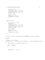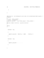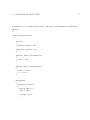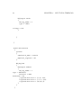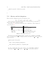
1
TIBERCAD User Manual
Fabio Sacconi, Matthias Auf der Maur,
Michael Povolotskyi, Giuseppe Romano,
Alessandro Pecchia, Gabriele Penazzi,
Stefano Bellocchio, Aldo Di Carlo
May 12, 2009
TIBERCAD User Manual
c TiberCAD authors (F. Sacconi, M. Auf der Maur, M. Povolotskyi,
G. Romano, A. Pecchia, G. Penazzi, S. Bellocchio, A. Di Carlo), 2008
Document revision 1.2.2-1446
Contents
Contents
I
Installation instructions
V
1 Overview
1.1 Intoduction to numerical simulation
1.1.1 Input file structure . . . . .
1.2 Definition of physical and boundary
1.2.1 Using ISE-TCAD . . . . .
1.2.2 Using GMSH . . . . . . . .
1.3 Simulation environments . . . . . .
1
1
2
3
4
4
7
with TiberCAD . .
. . . . . . . . . . . .
regions in TiberCAD
. . . . . . . . . . . .
. . . . . . . . . . . .
. . . . . . . . . . . .
. . .
. . .
. .
. . .
. . .
. . .
.
.
.
.
.
.
.
.
.
.
.
.
.
.
.
.
.
.
.
.
.
.
.
.
.
.
.
.
.
.
.
.
.
.
.
.
2 Getting started 1D
9
3 Getting started 2D
17
4 Input for TiberCAD
4.1 Description of Input file structure
4.2 Device section . . . . . . . . . .
4.3 Scale section . . . . . . . . . . .
4.4 Models section . . . . . . . . . .
4.4.1 options block . . . . . . .
4.4.2 physical model block . . .
4.4.3 BC region block . . . . .
4.5 Solver section . . . . . . . . . . .
4.6 Physics section . . . . . . . . . .
4.7 Simulation section . . . . . . . .
4.8 Output description . . . . . . . .
4.9 Example of Input file . . . . . . .
27
27
28
30
31
33
34
34
35
39
39
40
41
.
.
.
.
.
.
.
.
.
.
.
.
I
.
.
.
.
.
.
.
.
.
.
.
.
.
.
.
.
.
.
.
.
.
.
.
.
.
.
.
.
.
.
.
.
.
.
.
.
.
.
.
.
.
.
.
.
.
.
.
.
.
.
.
.
.
.
.
.
.
.
.
.
.
.
.
.
.
.
.
.
.
.
.
.
.
.
.
.
.
.
.
.
.
.
.
.
.
.
.
.
.
.
.
.
.
.
.
.
.
.
.
.
.
.
.
.
.
.
.
.
.
.
.
.
.
.
.
.
.
.
.
.
.
.
.
.
.
.
.
.
.
.
.
.
.
.
.
.
.
.
.
.
.
.
.
.
.
.
.
.
.
.
.
.
.
.
.
.
.
.
.
.
.
.
.
.
.
.
.
.
.
.
.
.
.
.
.
.
.
.
.
.
.
.
.
.
.
.
.
.
.
.
.
.
.
.
.
.
.
.
.
.
.
.
.
.
.
.
.
.
.
.
.
.
.
.
.
.
.
.
.
.
.
.
.
.
.
.
.
.
.
.
.
.
.
.
.
.
.
.
.
.
.
.
.
.
.
.
.
.
.
.
.
.
II
CONTENTS
5 Simulation of strain
5.1 Theory . . . . . . . . . . . . . . . . . . . . . . . . .
5.2 Models section parameters . . . . . . . . . . . . . .
5.2.1 Substrate boundary condition . . . . . . . .
5.2.2 External pressure boundary condition . . . .
5.2.3 Extended device boundary condition . . . .
5.3 Solver parameters . . . . . . . . . . . . . . . . . . .
5.3.1 Structure with a substrate . . . . . . . . . .
5.3.2 Structure without a substrate (freestanding)
5.3.3 Additional parameters . . . . . . . . . . . .
5.4 Physics section parameters . . . . . . . . . . . . . .
5.5 Output . . . . . . . . . . . . . . . . . . . . . . . . .
.
.
.
.
.
.
.
.
.
.
.
53
53
53
54
54
55
55
55
55
56
58
58
.
.
.
.
.
.
.
.
.
.
.
.
.
.
.
61
61
61
61
63
66
67
69
71
72
72
72
73
75
76
76
.
.
.
.
.
77
77
77
78
79
80
8 Envelope Function Approximation
8.1 Models section parameters . . . . . . . . . . . . . . . . . . . . . . . . . .
8.2 Solver parameters . . . . . . . . . . . . . . . . . . . . . . . . . . . . . . .
83
83
84
.
.
.
.
.
.
.
.
.
.
.
.
.
.
.
.
.
.
.
.
.
.
.
.
.
.
.
.
.
.
.
.
.
.
.
.
.
.
.
.
.
.
.
.
6 Drift-diffusion simulation of electrons and holes
6.1 Theory . . . . . . . . . . . . . . . . . . . . . . . . . . . . .
6.2 Plot variables . . . . . . . . . . . . . . . . . . . . . . . . .
6.3 Models section . . . . . . . . . . . . . . . . . . . . . . . .
6.3.1 Recombination models . . . . . . . . . . . . . . . .
6.3.2 Thermoelectric power models . . . . . . . . . . . .
6.3.3 Mobility models . . . . . . . . . . . . . . . . . . . .
6.3.4 Boundary conditions . . . . . . . . . . . . . . . . .
6.4 Physics section . . . . . . . . . . . . . . . . . . . . . . . .
6.4.1 Simple semiconductor model . . . . . . . . . . . . .
6.4.2 Default semiconductor model . . . . . . . . . . . .
6.4.3 Special options for Schrödinger-Poisson calculations
6.5 Solver section . . . . . . . . . . . . . . . . . . . . . . . .
6.5.1 Parameters for PETSc solvers . . . . . . . . . . . .
6.5.2 Parameters for the TIBERCAD nonlinear solver . . .
6.5.3 Parameters for the PARDISO linear solver . . . . .
7 Heat Balance simulation
7.1 Heat equation . . . . . . . . . . . . .
7.2 Physical model . . . . . . . . . . . .
7.2.1 Electron and hole dissipations
7.2.2 Boundary conditions . . . . .
7.3 Output data . . . . . . . . . . . . . .
.
.
.
.
.
.
.
.
.
.
.
.
.
.
.
.
.
.
.
.
.
.
.
.
.
.
.
.
.
.
.
.
.
.
.
.
.
.
.
.
.
.
.
.
.
.
.
.
.
.
.
.
.
.
.
.
.
.
.
.
.
.
.
.
.
.
.
.
.
.
.
.
.
.
.
.
.
.
.
.
.
.
.
.
.
.
.
.
.
.
.
.
.
.
.
.
.
.
.
.
.
.
.
.
.
.
.
.
.
.
.
.
.
.
.
.
.
.
.
.
.
.
.
.
.
.
.
.
.
.
.
.
.
.
.
.
.
.
.
.
.
.
.
.
.
.
.
.
.
.
.
.
.
.
.
.
.
.
.
.
.
.
.
.
.
.
.
.
.
.
.
.
.
.
.
.
.
.
.
.
.
.
.
.
.
.
.
.
.
.
.
.
.
.
.
.
.
.
.
.
.
.
.
.
.
.
.
.
.
.
.
.
.
.
.
.
.
.
.
.
.
.
.
.
.
.
.
.
.
.
.
.
.
.
.
.
.
.
.
.
.
.
.
.
.
.
.
.
.
.
.
.
.
.
.
.
.
.
.
.
.
.
.
.
.
.
.
.
.
.
.
.
.
.
.
.
.
CONTENTS
.
.
.
.
84
85
85
86
9 Simulation opticskp
9.1 Output . . . . . . . . . . . . . . . . . . . . . . . . . . . . . . . . . . . . .
87
88
10 Simulation opticalspectrum
10.1 Output . . . . . . . . . . . . . . . . . . . . . . . . . . . . . . . . . . . . .
89
90
11 Quantum dispersion
11.1 Solver options . . . . . . . . . . . . . . . . . . . . . . . . . . . . . . . . .
11.2 Output . . . . . . . . . . . . . . . . . . . . . . . . . . . . . . . . . . . . .
91
91
92
12 Quantum Density
12.1 Output . . . . . . . . . . . . . . . . . . . . . . . . . . . . . . . . . . . . .
93
94
Bibliography
95
8.3
8.4
8.2.1 Eigenvalue problem parameters .
8.2.2 Schrödinger equation parameters
Physical Models parameters . . . . . . .
Output . . . . . . . . . . . . . . . . . . .
III
.
.
.
.
.
.
.
.
.
.
.
.
.
.
.
.
.
.
.
.
.
.
.
.
.
.
.
.
.
.
.
.
.
.
.
.
.
.
.
.
.
.
.
.
.
.
.
.
.
.
.
.
.
.
.
.
.
.
.
.
.
.
.
.
.
.
.
.
IV
CONTENTS
Installation instructions
In the following, VERSION denotes the version number of the TIBERCAD release you
downloaded and INSTALLPATH denotes the directory where TIBERCAD gets installed.
Version 2.3.0 of GMSH (http://www.geuz.org/gmsh) will be installed together with
TIBERCAD. For the Linux version of GMSH you need OpenGL libraries installed on
your system.
Prerequisites
Get the installer package for your OS/architecture from http://www.tibercad.org or
by contacting [email protected]. Table 1 lists the packages available for download.
To run TIBERCAD you will also need a license file that you will have to copy into the
installation directory of TIBERCAD.
In the Windows version, some graphical features such as graphical convergence monitors are only available if an X Window server is installed and running.
Windows installation procedure
To install TIBERCAD in Windows, run the setup program tibercad-version_setup.exe.
During the installation you can choose the installation directory. After finishing installation, copy your license file (tibercad.lic) into the license subdirectory of the TIBERCAD
installation directory (INSTALLPATH/license), without changing its filename.
installer package name
Target architecture
tibercad-version_setup.exe
Windows 32-bit
tibercad-version_installer.bin Linux 32-bit self-extracting installer
Table 1: Installer packages
V
VI
CONTENTS
Linux installation procedure
To install TIBERCAD in Linux, download and run the self-extracting installer tibercadversion_installer.bin and follow the installation instructions.
After installation, copy your license file (tibercad.lic) into the ‘license’ subdirectory
of the TIBERCAD installation directory (INSTALLPATH/license) without changing the filename. You can also provide the license file during installation.
The standard method to launch TIBERCAD is by means of a shell script that is
installed alongside the TiberCAD executable. It takes care of setting all necessary environment variables. If for some reason you have to run the executable directly, remember
to set TIBERCADROOT to the TiberCAD installation directory (INSTALLPATH).
Quick start guide
In the ‘examples’ subdirectory you can find several examples ready to run. They are the
same as the tutorials on http://www.tibercad.org/documentation/tutorial/list.
Windows
Open Windows Explorer and go to the TIBERCAD installation directory. If you have
write permission in the installation directory, you can browse to an examples directory
and start the simulation by double clicking the input file, e.g. bulk.tib in Example 0. If
not, copy the whole directory to a location in your personal area and run the examples
from there.
If you cannot run TIBERCAD by double clicking an input file (*.tib), then the input
files are probably not correctly associated with the TIBERCAD executable. In this case,
try to establish the association by right-clicking the input file, choosing open with...
→ Choose Program... → Browse..., browsing to the TIBERCAD installation directory
and choosing the TIBERCAD executable, tibercad.exe. A directory containing the
simulation results will be created with the name provided in the input file.
Linux
After the correct installation of TIBERCAD you should be able to run TIBERCAD from the
command line using the command tibercad. If not, you probably have to add the bin
subdirectory of the TIBERCAD installation directory to your PATH environment variable or
start the TIBERCAD executable using the absolute path (INSTALLPATH/bin/tibercad).
Copy the directory of the example you want to run, e.g. bulk Si, to your home directory
or any place you have write permissions for. Change to the newly created directory and
run TIBERCAD by (assuming Example 0)
CONTENTS
VII
$ tibercad bulk.tib
A directory containing the simulation results will be created with the name provided in
the input file.
Bug reports / Feedback
Please send bug reports, feedback or suggestions to [email protected]. When submitting bug reports, please always include the full version number of TIBERCAD you are
running. The full version number appears in the first line of output when running the
program:
$ tibercad
TiberCAD version 1.0.0-961
Usage: tibercad <inputfile>
Chapter 1
Overview
1.1
Intoduction to numerical simulation with TiberCAD
TiberCAD is a multiphysics software tool; it comprises a set of solvers, called simulation
models, each one describing a physical problem to be solved, e.g. DriftDiffusion (to solve
Poisson and DriftDiffusion equations), EFASchroedinger (to solve Schroedinger equation
in envelope function approximation), Macrostrain (to calculate macroscopical strain with
an elastic model) and others.
Similarly to other device CADs, TiberCAD requires that one follows a three-step
procedure.
In a first step the device geometry must be sketched, giving all the geometrical information needed by the simulations. This can be performed by means of a text file
or with the help of a graphical tool. During this procedure one or more mesh regions
and boundary regions have to be defined: in a following stage the mesh regions will be
associated to materials and boundary regions to device contacts (boundary conditions in
general).
The second step consists in running a mesher tool, which reads the geometry file
and sets up the computational mesh used to discretize the partial differential equations
representing the physical models to be solved. For this procedure TIBERCADmakes use
of the GPL software gmsh. Optionally, mesh outout provided by other meshers, such
as the one included in ISE-TCAD tool, are also supported. The output of the meshing
procedure is a mesh file that contains information about the space discretization as well
as the mesh regions and the boundary regions.
In the last step the actual simulations are performed. Together with the mesh information (comprised in the mesh file ), TiberCAD requires an input file which associates
materials to mesh regions, defines the physical properties and physical models to be
1
2
CHAPTER 1. OVERVIEW
applied, and the type of calculations to be performed.
Details about the modeler and mesher tools can be found in the specific user-manuals.
Here we deal primarily with the TiberCAD input file. However, in discussing examples
of 1D, 2D and 3D simulations, we will also describe in some detail the geometry input
files used to run gmsh.
1.1.1
Input file structure
TiberCAD input file is a text file which includes a description of the device structure,
the definition of the solvers to be executed, with all the relevant physical and numerical
parameters for each of them.
The input file is organized into several sections, each describing a different aspect of
the problem to be solved. The strategy employed is similar to other commercial T-CAD
tools and requires some practice to reach a good level of familiarity. We strongly suggest
to read first the following chapters (Getting Started 1 and 2) in this manual and then
study the input files provided in the examples directory and try to modify them, before
writing your own input file from scratch. The example files touch all current features
implemented in the code.
Let’s see an overview of the main features of the input file The core of the input file
comprises three sections, called Device, Models and Simulation:
$Device
{
Region Si_channel
{
material= Si
doping = 1e16
}
Region gate_oxide
{
material= SiO2
}
...
}
$Models
{
1.2. DEFINITION OF PHYSICAL AND BOUNDARY REGIONS IN TIBERCAD
3
model driftdiffusion
{
simulation_name= dd
}
...
}
$Simulation
{
solve= dd
}
The section Device is used to associate one or more mesh regions to a material and
to a set of physiscal properties such as doping concentrations, doping levels, etc. The
section Model is used to define the physical models to be solved. Each physical model
can be applied to the whole device, or to a set of regions of the device, (defined in Device
section). Finally, Simulation section states the type of calculation to be executed, that
is the simulation to be solved. These sections will be described in full details in the
following.
Besides these main sections, there other other two, called Solver and Physics, where
some parameters can be set, respectively for the numerical solvers and for the physical
models. The aim of these sections is to give the user the maximum of flexibility to
tune his/her simulation. Especially regarding the Solver case, values of the numerical
parameters have been already tuned for each application and should be modified only
by an advanced user.
1.2
Definition of physical and boundary regions in
TiberCAD
Let’see now in more detail how to associate physical information to the regions of the
device model and how to define the boundary regions, that is contacts or, in general,
regions where some kind of boundary condition is to be applied.
When TIBERCAD is run, it reads the mesh file which contains the finite element grid
which meshes the geometrical description of the device or nanostructure, and which will
be the basis of PDE discretization.
As we have seen before, to execute the proper simulations, TIBERCAD needs some information about the physical and boundary regions associated with the mesh. A physical
4
CHAPTER 1. OVERVIEW
region associates all the elements corresponding to an homogeneous part of the device
(usually related to the same material or doping). In TIBERCAD, these regions are referred
to as mesh regions.
As for boundary regions, they are needed to specify boundary conditions (b.c.) for
the solution of the PDEs of our simulation. By default, to all the external boundary of
the device a Neumann b.c. is imposed, meaning null derivative of electric field and zero
flux of current normal to the boundary. These are the usual b.c. applied in the simulation
of electronic devices; in particular, these conditions are implicitly satisfied by using the
finite element formulation.. Usually, however, one needs to impose also specifical b.c.
to the device, relative, most often, to contacts of some kind (ohmic, schottky), but also
heat and temperature b.c. or reference substrates for strain calculations. These regions,
(constituted by surfaces, lines or points, respectively for 3D, 2D and 1D simulations) are
called in TIBERCAD boundary regions.
It is important to know that the information about the physical and boundary regions
must be present in the mesh file before it is read by TIBERCAD, and thus have to be
produced by making use of the modeling/mesher software. As for now, TIBERCAD
supports the mesh output of the following software tools: GMSH v.2 and ISE-TCAD
v.9.5.
1.2.1
Using ISE-TCAD
By means of the utility DEVISE of ISE-TCAD v.9.5, it is possible to design and mesh
a device; after the meshing has been successfully performed, an output file is produced,
with the extension .grd. This file contains the description of the mesh and also the
list of the user defined material regions and contact regions. By reading this .grd file
in TIBERCAD, one can refer to the ISE TCAD material regions, simply with the userdefined name, which is present in the .grd file. This name should be unique in the whole
device. In the same way, ISE TCAD Boundary regions (Contacts) can be referred to in
TIBERCAD by means of their user-defined name, present in the .grd output file, too.
1.2.2
Using GMSH
If GMSH program is used to model and mesh the device, a bit more care has to be
taken. Here we introduce the procedure to be followed; in the following tutorials (Getting
started... the subject will be considered in detail with a step-by-step description. See
also the GMSH user manual (http://geuz.org/gmsh) for further details.
In the context of GMSH, it is possible to define several 1, 2 and 3D Physical Entities.
These Physical Entities allow to associate one or more geometrical entities to a single
numerical ID or, better, to a string label, so that several mesh regions and boundary
1.2. DEFINITION OF PHYSICAL AND BOUNDARY REGIONS IN TIBERCAD
5
regions can be defined and referred to by TiberCAD. Here is a simple example of a
script to generate a 1D geometrical model ( *.geo) file in GMSH: (see also chapter 2)
Point(1) = {-25,0,0,0.5};
Point(2) = {0,0,0,0.002};
Point(3) = {25,0,0,0.5};
Line(1) = {1,2};
Line(2) = {2,3};
Physical
Physical
Physical
Physical
Line("p_side") =
Line("n_side") =
Point("cathode")
Point("anode") =
{2};
{1};
= {3};
{1};
Here, first the geometrical entities Points and Lines are defined.
In the definition of the geometrical Points, the three first expressions inside the
braces on the right hand side give the three X, Y and Z coordinates of the point ; the
last expression (0.5 or 0.002 in this example) sets the characteristic mesh length at
that point, that is the size of a mesh element, defined as the length of the segment for
a line mesh element, the radius of the circumscribed circle for a triangle mesh element
and the radius of the circumscribed sphere for a tetrahedron mesh element. Thus, the
smaller is the value of the characteristic mesh length, the greater is the mesh density
close to that point. The size of the mesh elements will then be computed in GMSH by
linearly interpolating these characteristic lengths in the whole mesh.
In the definition of a geometrical Line, the two expressions inside the braces on the
right hand side give the identification numbers of the start and end Points of the line.
Then, two physical regions are defined, each associated to one of the two geometrical
entities: Physical Line(n side) and Physical Line(p side). The expression(s) inside
the braces on the right hand side give, in general, the identification numbers of all the
geometrical lines that need to be grouped inside the Physical Line.
In this way, these physical regions are made available for TIBERCAD, and will be used
to associate them to a TIBERCAD region through the keyword Region , as follows:
Region n_side
{
............
............
Region
p_side
6
CHAPTER 1. OVERVIEW
{
.............
...........
It is also possible to group more than one physical region in a single Device Region,
with the keyword mesh regions, as follows:
Region reg_1
{
mesh_regions
= (region1, region2)
............
Region reg_2
{
mesh_regions
= (region3, region4)
...........
Note that, in this case, region1, region2, region3, region4 are the labels previously
defined inside GMSH, while reg 1 and reg 2 are names chosen by user for his convenience.
Then, in the GMSH script, two Physical Point are defined, anode and cathode,
and associated to the first and to the last point of our 1D device. These points are
needed to impose some boundary conditions and in this way they are made available for
TiberCAD, and will be used to associate each of them to a boundary condition region,
through the keyword BC Region:
BC_Regions
{
BC_Region cathode
{
.........
......................
BC_Region anode
{
........
....................
1.3. SIMULATION ENVIRONMENTS
7
As before, it is possible group more boundary regions in a single BC Region, with
the keyword BC reg numb
BC_Regions
{
BC_Region cathode
{
BC_reg_numb = (contact1,
contact2)
......................
....................
Again, in this second case, cathode is a label chosen by user, while contact1 and
contact2 are labels previously defined inside GMSH.
In 2D case, a set of Physical Surface will be defined to be used as mesh regions,
while Physical Line is used for boundary regions.
Finally, in 3D case, Physical Volume is used to define mesh regions, while Physical Surface is used to define boundary regions.
1.3
Simulation environments
TIBERCAD allows to compute different physical models in different parts of a device or
nanostructure by coupling in a general way different simulation environments. A simulation environment is composed by all the physical regions to which a particular model is
assigned. A simulation environment is therefore defined by the mesh elements belonging
to its physical regions and by the simulation model which has been associated to these
regions. This association is made possible by the definition of TIBERCAD Regions and
Clusters. Different simulation environments can have physical regions in common. In
this way, each simulation is run on a subset of the device and can be possibly coupled
(even self-consistently) with a simulation run on a different subset of the device corresponding to a simulation environment with a non-void intersection with the first one.
The coupling of the two simulations is performed by means of appropriate Boundary
Conditions (e.g. Current Density, Voltage, ...). In principle, the two simulation environments can refer to two simulations at different scale, e.g. atomistic tight-binding and
macroscopic drift-diffusion. This allows an effective multi-scale simulation of the device
to be studied.
8
CHAPTER 1. OVERVIEW
Chapter 2
Getting started 1D
In this section we will see, step by step, how to use TIBERCAD to simulate numerically
a semiconductor device. As a very simple example we will refer to the Tutorial 0 (Si
bulk) that you can find in the Tutorials directory.
Step 1: Modeling the device
As a first step, we have to model the device. To do so, you can use DEVISE module
of ISE-TCAD 9.5 software package or GMSH program. Here we’ll see in details the
procedure for GMSH. There are two possible ways to use GMSH:
1. Interactive, using the graphical interface
2. Using a script file.
In the following we’ll see how to write a basic GMSH script (bulk.geo); for any details
please refer to GMSH manual GMSH (http://geuz.org/gmsh/).
In a GMSH script, several variables can be defined and given a value in this way:
L = 1;
d = 0.01;
these are valid GMSH variables: L is just the length of the Si sample; d is the value
of a characteristic mesh length (see below).
• Definition of geometrical entities Points:
Point(1) = {0, 0, 0, d};
Point(2) = {L, 0, 0, d};
9
10
CHAPTER 2. GETTING STARTED 1D
In the definition of a geometrical point, the three first expressions inside the braces
on the right hand side give the three X, Y and Z coordinates of the point; the last
expression (d) sets the characteristic mesh length at that point, that is the size of a
mesh element, defined as the length of the segment for a line mesh element, the radius of
the circumscribed circle for a triangle mesh element and the radius of the circumscribed
sphere for a tetrahedron mesh element.
Thus, the smaller is the value of d, the greater is the mesh density close to that point.
The size of the mesh elements will then be computed in GMSH by linearly interpolating
these characteristic lengths in the whole mesh.
N.B.: In a 1D simulation it is assumed that the geometrical model is restricted to
the x axis. Any other geometrical orientation could give impredictable results.
• Definition of geometrical entity Line:
Line(1) = {1, 2};
The two expressions inside the braces on the right hand side give the identification
numbers of the start and end points of the line.
• Definition of the physical entity Physical Line 1:
Physical Line(1) = {1};
The expression(s) inside the braces on the right hand side give the identification
numbers of all the geometrical lines that need to be grouped inside the physical line.
In this way, in general, physical regions are created which associate together geometrical regions, and then the related mesh elements, which share some common physical
properties. It’s only these physical regions which can be referred to outside GMSH. In
TIBERCAD, this is done by associating one or more physical regions to a TiberCAD
region through the keyword mesh regions (see in the following).
• Definition of two physical entities Physical Point:
Physical Point(1) = {1};
Physical Point(2) = {2};
Beginning from GMSH v.2, it is possible, alternatively, to assign more convenient
Physical Names to the Physical entities, instead of numerical IDs. Physical Names
consist of strings enclosed between quotation marks. The syntax is the following:
11
Physical Line("bulk") = {1}
............
Physical Point("Anode") = {1};
N.B.: In general, in a n-Dimension (nD) simulation, (n-1)D physical regions (points
in 1D, lines in 2D, surfaces in 3D) are used by TIBERCAD to impose the required boundary
conditions. Each (n-1)D physical region defined in this way in GMSH will be associated
in TIBERCAD to a boundary condition region, through the keyword BC reg numb.
Thus, in this case, Physical points 1 and 2 will be associated respectively to two BC
regions (see in the following).
Step 2: Meshing the device
The .geo script file with the geometrical description can be run in GMSH, to display the
modelled device and to mesh it through the GMSH graphical interface. Alternatively, a
non-interactive mode is also available in GMSH, without graphical user interface. For
example, to mesh this 1D tutorial in non-interactive mode, just type:
gmsh bulk.geo -1 -o bulk.msh
where bulk.geo is the geometrical description of the device with GMSH syntax; -1
means 1D mesh generation;
some command line options are:
-1, -2, -3 to perform 1D, 2D or 3D mesh generation,
-o mesh file.msh to specify the name of the mesh file to be generated
In this way, a .msh has been generated and is ready to be read in TIBERCAD.
Step 3: TiberCAD Input file
Now we have to write down the TIBERCAD input file (see bulk.tib in the Tutorials).
1 - Definition of Device Regions
First, we have to list all the TIBERCAD Regions present in our device: a TIBERCAD
Region is usually a somehow physically homogeneous region of the device or the nanostructure we are going to model, featuring the same material and possibly the same
doping.
$Device
{
Region bulk
12
CHAPTER 2. GETTING STARTED 1D
{
mesh_regions = 1
material = Si
doping = 1e16 doping_type = donor
}
}
In this example, the TIBERCAD Region bulk is made of Silicon and n-doped with a
concentration 1016 cm−3 .
Through the keyword mesh regions, one or more of the physical regions (Physical
Lines in 1D, Physical Surfaces in 2D, Physical Volumes in 3D) previously defined in the
GMSH mesh can be associated to the present TIBERCAD Region.
With mesh regions = 1, we associate the Physical Line 1, defined in the Step 1, to
the TIBERCAD Region bulk.
2 - Definition of Simulation
Now we define the Simulation driftdiffusion 1 : it belongs to the class driftdiffusion
Models
{
model driftdiffusion
{
options
{
simulation_name = driftdiffusion_1
physical_regions = all
}
The TIBERCAD simulation driftdiffusion 1, belonging to the model driftdiffusion,
will be applied to the whole device structure (physical regions = all ).
3 - Definition of Boundary Conditions
The anode and cathode contacts of our 1D Si sample are defined as Boundary conditions regions (BC Region anode, BC Region cathode) in the following way:
BC_Region anode
{
BC_reg_numb = 1
13
type = ohmic
voltage = @Vb
}
BC_Region cathode
{
BC_reg_numb = 2
type = ohmic
voltage = 0.0
}
Both contacts are defined as ohmic, cathod is assigned a fixed voltage = 0.0, while anode
voltage is given by the value of the variable Vb (voltage = @Vb).
Through the keyword BC reg numb, one or more of the (n-1)-Dimension physical
regions (Physical Points in 1D, Physical Lines in 2D, Physical Surfaces in 3D) previously
defined in the GMSH mesh can be associated to the present TIBERCAD BC Region.
With BC reg numb = 1, we associate the Physical Point 1, defined in the Step 1, to the
TIBERCAD BC Region anode; with BC reg numb = 2, we associate the Physical Point
2, defined in the Step 1, to the TIBERCAD BC Region cathode.
Alternatively, one can make use of the physical names associated to the physical
regions in the meshing tool. In this case, we simply associate the (n-1)D physical region,
respectively “anode” and “cathode”, by means of the TIBERCAD BC Region name:
BC_Region anode
{
type = ohmic
voltage = @Vb
}
BC_Region cathode
{
type = ohmic
voltage = 0.0
}
Note that, in this case, the TIBERCAD BC Region name needs to be identical to
one of the physical names defined during the modeling of the device with GMSH.
14
CHAPTER 2. GETTING STARTED 1D
4 - Definition of Simulation parameters
The variable Vb is specified in the sweep block, in the Solver section
sweep
{
simulation = driftdiffusion_1
variable = Vb
start = 0.0
stop = 1
steps = 10
}
In this way, the simulation driftdiffusion 1 is performed for 10 ( steps = 10 ) values
of the anode voltage (variable = Vb), between 0 and 1.
5 - Definition of Execution parameters
In the Simulation section, we decide which simulations to perform and in which order ;
we set solve = sweep, to execute the sweep which run driftdiffusion 1 simulation for
the specified loop.
$Simulation
{
#searchpath = .
meshfile = bulk.msh
dimension = 1
temperature = 300
solve = sweep
resultpath = output
output_format = grace
plot = (Ec, Ev, ContactCurrents)
}
Output files with conduction and valence band profiles (plot = Ec,Ev..) and all the
calculated values of the current at the contacts (ContactCurrents) (the IV characteristic)
are generated.
Step 4: Run TiberCAD
Now we can run TiberCAD:
15
tibercad bulk.tib
The generated Output files are:
driftdiffusion materials.dat: material (mesh) regions, in this case just region 1
driftdiffusion nodal.dat: nodal quantities (here conduction and valence band)
sweep driftdiffusion Vb.dat : integrated current at the two contacts for each
sweep step.
16
CHAPTER 2. GETTING STARTED 1D
Chapter 3
Getting started 2D
In this second example we will refer to the Tutorial 4 (Si n-Mosfet) that you can find
in the Tutorials directory.
Step 1: Modeling the device
Again, as a first step, we have to model the device.
We’ll see in some details how to design and mesh a mosfet device with GMSH.
• In the GMSH script mosfet.geo , several variables are defined and given a value in
this way:
lsub=0.03;
lacc=0.002;
lct=0.0005;
lg=0.0015;
lh=0.01;
lc=0.0005;
these variables are used in the script to assign proper values to the mesh characteristic lengh of the defined Points
Lg_2 = 0.0375;
d = 0.01;
Ls = 0.1;
h = 0.25;
b = 0.0025;
o = 0.005;
17
18
CHAPTER 3. GETTING STARTED 2D
xd = Lg_2 + d;
xd2 = Lg_2 + d / 2;
xmax = xd + Ls - d;
These other convenient variables are used to parametrize the most relevant geometrical
features, such as channel length, oxide thickness, and so on.
• Geometrical Points and Lines are defined to design the device structure; the
fourth parameter in Point assignement is the characteristic length associated to
that point: this is an essential feature to control the mesh density and refine it
where necessary (usually n the channel region).
N.B.: In a 2D simulation it is assumed that the geometrical model is restricted to the
xy -plane (z = 0). Any other geometrical orientation could give impredictable results.
Point(1) = {0, -h, 0, lsub};
Point(2) = {0, 0, 0, lc};
Point(3) = {xmax,-h,0.0,lsub};
Point(4) = {-xmax,-h,0.0,lsub};
Point(5) = {xmax,0,0.0,lh};
Point(6) = {-xmax,0,0.0,lh};
..........................
Line(1) = {4,1};
Line(2) = {3,13};
Line(6) = {4,14};
Line(7) = {10,9};
Line(8) = {12,2};
Line(9) = {8,7};
Line(10) = {11,8};
Line(11) = {9,12};
Line(13) = {7,6};
..........................
• Definition of a surface: first a line loop is composed, listing all the lines constituting the boundary of the surface; then this line loop is assigned to a Plane
Surface object (this procedure can be alternatively performed throgh the graphical
interface).
Line Loop(40) = {28,2,-34,33,8,29,-31,-30,-6,1};
Plane Surface(41) = {40};
..........................
19
• Definition of the Physical surfaces : each of them is composed by one or more
geometrical Plane Surface. For example, Physical surface 2 comprises the
two separated contact regions, while Physical surface 3 corresponds to the oxide
region.
The Physical surfaces are the 2D Physical regions of the mesh and will be assigned to the related TIBERCAD regions through the keyword mesh regions (see
Step )
Physical Surface(1) = {41}; // n-Si
Physical Surface(2) = {44,47}; // n+-Si
Physical Surface(3) = {46}; // SiO2
• Definition of the Phisical Lines: In this 2D simulation, 1D physical regions are
used to carry information about boundary condition regions. In other word, each
Phisical Line corresponds to a boundary condition (a contact in the case of a
driftdiffusion calculation): thus Physical Line 1 refers to source contact, P.L. 2 to
gate contact, P.L. 3 to drain contact. The numerical identifications of these Phisical Lines will be asigned to TIBERCAD BC regions by means of the BC reg numb
instruction.
Physical Line(1) = {13}; // source
Physical Line(2) = {39,38}; // gate
Physical Line(3) = {19}; // drain
In fig. 3.1 the obtained geometrical model is shown.
Step 2: Meshing the device
The .geo script file with the geometrical description can be run in GMSH, to display
the modelled device and to mesh it through the GMSH graphical interface (see fig. 3.2).
Alternatively, a non-interactive mode is also available in GMSH, without graphical user
interface. For example, to mesh this 2D tutorial in non-interactive mode, just type:
gmsh mosfet.geo -2 -o mosfet.msh
Step 3: TiberCAD Input file
Now we have to write down the TIBERCAD input file (see mosfet.tib in the Tutorials).
20
CHAPTER 3. GETTING STARTED 2D
Figure 3.1: Geometrical structure as defined by GMSH modeller
Figure 3.2: 2D Mesh for the mosfet device obtained with GMSH
21
1 - Definition of Device Regions
Three TIBERCAD regions are defined: to each of them, one mesh region is associated,
that is the Phisical Surfaces 1, 2 and 3 defined in Step 1. However, in general more than
one mesh region can be associate to a single TIBERCAD region, if this is convenient.
Region substrate
{
mesh_regions = 1
material = Si
doping = 1e18 doping_type = acceptor
}
Region contact
{
mesh_regions = 2
material = Si
doping = 5e19 doping_type = donor
}
Region oxide
{
mesh_regions = 3
material = SiO2
}
2 - Definition of Simulation
Now we define the Simulation dd : it belongs to the class driftdiffusion
model driftdiffusion
{
options
{
simulation_name = dd
physical_regions = all
}
22
CHAPTER 3. GETTING STARTED 2D
We declare two driftdiffusion physical models: the first defines a srh recombination model (see 6.3.1); the second defines a field-dependent mobility model for
electrons which implements a doping dependence for the low-field mobility (see 6.3.3).
physical_model recombination
{
model = srh
}
physical_model electron_mobility
{
model = field_dependent
low_field_model = doping_dependent
}
3 - Definition of Boundary Conditions
The source, drain and gate contacts of the Mosfet device are defined as Boundary
conditions regions (BC Region source , BC Region drain, BC Region gate ) in the
following way:
BC_Region gate
{
BC_reg_numb = 2
type = schottky
barrier_height = 3.0
voltage = @Vg[0.0]
}
BC_Region source
{
BC_reg_numb = 1
type = ohmic
23
voltage = 0.0
}
BC_Region drain
{
BC_reg_numb = 3
type = ohmic
voltage = @Vd[0.5]
}
To each of the BC regions, one BC reg numb is assigned, that is one of the Physical
Lines 1,2, 3 defined in Step 1, which represent the contact regions.
Note that, while source and drain are defined as type= ohmic, gate BC region is
defined as type = schottky; barrier height = 3.0 specifes the metal/oxide interface barrier
and depends on the contact metal workfunction.
Drain voltage is defined as @Vd[0.5] and gate voltage as @Vg[0.0]. This specifies
that the value of the voltage will be determined at each moment of the simulation, by
the value of the two variables Vd and Vg, which will be assigned in the sweep definition.
4 - Definition of Simulation parameters
Two sweeps are requested for this simulation, that is an external loop on Vg (the gate
voltage) and an internal loop on Vd (the drain voltage) for each value of Vg; in this way,
the IV drain characteristics for a series of gate biases are obtained in output.
sweep_1
{
#
}
simulation = dd
variable = Vd
start = 0.0
stop = 2.0 #0.1
steps = 200 #200 #1
plot_data = true
sweep_2
{
variable = Vg
24
CHAPTER 3. GETTING STARTED 2D
start = -0.1
stop = 0.5
steps = 6
simulation = sweep_1
#simulation = driftdiffusion
}
5 - Definition of Execution parameters
In the Simulation section , we decide the simulation dimension (dimension = 2 ), then
which simulations to perform and in which order ; we set solve = sweep 2, to execute the
external gate voltage sweep sweep 2 which in its turn call the sweep sweep 1 where drain
current is calculated for all the chosen drain voltage steps by running dd simulation.
$Simulation
{
meshfile = mosfet.msh
dimension = 2
temperature = 300
solve = sweep_2
resultpath = output_IV_char
output_format = vtk
plot = (Ec, Ev, QFermi_e, QFermi_h, eDensity, hDensity, eCurrent, hCurrent,
NetRecombination, EField, ElPotential, ContactCurrents)
}
Output files with conduction and valence band profiles, quasi-fermi levels, electron
and hole density, recombination, electric field and potential (plot = Ec,Ev,.....) will be
generated, together (ContactCurrents) with a file with all the calculated values of the
drain current at the contacts for each gate bias step (the IV characteristics).
Step 4: Run TiberCAD
Now we can run TiberCAD:
tibercad mosfet.tib
The generated Output files are:
25
driftdiffusion materials.vtk: information about the material regions of the device.
driftdiffusion nodal.vtk output for the nodal quantities which have been calculated, e.g. conduction and valence bands, (quasi)fermi levels, electron and hole density
and mobility.
driftdiffusion elemental.vtk output for the elemental quantities (e.g. electric field,
current density).
sweep 2 driftdiffusion Vg 0.000 Vd.dat and similar for all the Vg steps: drain
current characteristics for each Vg bias.
26
CHAPTER 3. GETTING STARTED 2D
Chapter 4
Input for TiberCAD
Input for TIBERCAD is composed by an input file e.g. ”input.tib” and a mesh file generated by a mesher software: as for now, mesh files from GMSH (*.msh, v.1 and v.2.0 )
and from ISE-TCAD (*.grd) are supported.
Be sure that the material files are in the correct directory (as specified in 4.7).
To run the program, type: tibercad input file name
4.1
Description of Input file structure
A valid input file for TIBERCAD is a text file with the structure described in the following.
In the whole input file, everything following a ’#’ is considered as a comment and is
disregarded; blank lines can be present anywhere and are disregarded too.
Input file is composed by several sections: each section begins with a sectionname preceded by ”$” (e.g. $Physics).
A section is enclosed between ”{” and ”}” brackets and is possibly composed (depending on the section) by a variable number of blocks enclosed between ”{” and ”}”
brackets.
Each block can be possibly composed by one or more blocks, each preceded by a
block-name.
The elementary block (parameters-block) is a block which contain zero or any
number of parameter assignements in the form:
”tagname = tagvalue”,
where
• ”tagname” is a string
• ”tagvalue” is a single numerical or string item or a list of items between ”(” and ”)”
parenthesis and separated by commas. e.g. (cathode, anode)
27
28
CHAPTER 4. INPUT FOR TIBERCAD
Format is free for the parameter assignements, provided that they are separated by
spaces. Everything which follows a ’#’ is considered as a comment and is disregarded.
For example:
driftdiffusion
{
coupling = poisson
nonlin_max_it = 70
nonlin_rel_tol = 1e-10
ls_max_step = 2
ksp_type = bcgs
}
Here and in the whole input file a string item can include a combination of characters,
special characters and numbers, but not spaces; if a space is found , the string item is
taken as terminated.
The input file is composed by the following sections:
Device, Scale, Models, Physics, Solver, Simulation
which will be described in the following.
4.2
Device section
$Device
{
Region buffer
{
.........
}
Region barrier_1
{
............
}
.................
}
In ”Device” section, two kinds of block can be present: the Region block and the
Cluster block.
4.2. DEVICE SECTION
29
The Region blocks contain the description of the device in continuous media approach; the Cluster blocks define each a group of regions (mesh regions) even with
different physical properties, but to be treated together somewhere in the simulation
(e.g. quantum calculation). In this way it is possible to refer to the set of these regions
simply by the Cluster name.
Each Region block must be preceded by the keyword ”Region”, followed by the
(single-word) name of the TiberCAD Region. The name of the TiberCAD Region
can coincide with the name of a mesh region, as defined during the modeling of the
device; in this case, if the keyword mesh regions is absent, the TiberCAD Region will
be associated to the mesh region identified by the name assigned to the TiberCAD
Region. Otherwise, the TiberCAD Region will be associated to the mesh regions
specified by the keyword mesh regions.
Region QWell
{
mesh_regions = (4,5)
# mesh_regions = 4
structure = wz
y-growth-direction = (1,0,-1,0)
z-growth-direction = (-1,2,-1,0)
x-growth-direction = (0,0,0,1)
material = GaN
doping = 1e17 doping_type = donor doping_level = 0.025
}
Here are the description of the available keywords for a Region block.
material (mandatory): name of the material associated to the present region, e.g Si;
it may be a ternary alloy, e.g AlGaAs, in this case keyword x described in the following
has to be present.
x : alloy concentration, expressed as the molar fraction of the first component of
the alloy; e.g. to express an alloy Alx Ga1−x As with molar fraction x = 0.2, that is
Al0.2 Ga0.8 As, we select AlGaAs for the keyword material, and 0.2 for the keyword x,
thus we write x = 0.2.
mesh regions : (a list of) region ID(s) or physical name(s) as specified in the meshing
program.
structure : crystal structure (wz = wurtzite, zb = zincblend)
x-growth-direction, y-growth-direction, z-growth-direction: Bravais vectors with Miller
indexes for wurtzite crystal (4 element vectors) or zincblende crystal (3 element vectors).
doping : doping concentration [cm−3 ]
doping type : donor or acceptor
30
CHAPTER 4. INPUT FOR TIBERCAD
doping level : energy level of the dopant [eV]
Each Cluster block must be preceded by the keyword ”Cluster”, followed by the
(single-word) name of the Cluster.
Cluster Quantum_1
{
mesh_regions
}
= (3,4,5)
mesh regions (mandatory): list of physical regions (region IDs or physical names) or
TIBERCAD region names, as specified in the meshing program, to be grouped in the
cluster.
Regions and Clusters represent the macroscopical description of the device or structure to be be simulated in TiberCAD. In the rest of the input file, the physical regions
associated to Models or Atomistic descriptions will be indicated by means of the
TiberCAD Region and Cluster names.
4.3
Scale section
The section ”Scale” is dedicated to the optional definition of Non-Continuous Media
regions for the device: these regions will be described and studied at a different scale (e.g.
atomistic, circuit level lumped model, etc.) As for now, just the atomistic description
is implemented. Atomistic blocks, if present, specify a possible atomistic description
associated to one or to a group of physical regions described by Region blocks. So,
for each Atomistic block defined in Input file, an atomic structure description will
be generated and used to solve a simulation problem with an atomistic approach. The
association to the physical (macroscopic) regions of the device allows the implementation
of multi-scale calculations.
Each Atomistic block must be preceded by the keyword ”Atomistic”, followed by
the (single-word) name of the atomistic region.
Atomistic TB_1
{
physical_regions = (barrier_1, qwell, barrier_2)
# physical regions to be described
# with atomistic model.
}
4.4. MODELS SECTION
31
Here are the description of the available keywords for an Atomistic block.
physical regions (mandatory): list of the physical regions (TiberCAD Regions or
Clusters ) of the device associated to an atomistic description. all (default) is used to
specify all the physical regions.
path (optional): path for importing an atomistic structure from an external file. xyz
and gen formats are supported, and are automatically recognized by file extension. Each
of the atom positions is imported as is, so the atom coordinates must be consistent with
the geometry of the device.
If no path is specified, the TiberCAD Atomistic Generator builds the atomistic
structure; it is constructed as a bulk crystal structure, covering with proper atomic
species the physical regions and taking in account the dimension of the problem (up to
now 1D structures are supported)............
Atomistic Generator options, to be put in the Atomistic section, are described in the
following.
reference region (mandatory): the Atomistic Generator can only build pseudomorphical heterostructures. A reference region must be defined to specify from which region
(TiberCAD Regions) to get structure parameters such as lattice constants, which
depend on the material defined in the reference region.
passivation (optional): no is default option. If set to no, no passivation is performed.
If yes is specified, a hydrogenation of the structure is performed, taking into account the
structure periodicity. Up to now, hydrogenation is supported fo Silicon structures.
preserve (optional): Default is none. In some cases it is requested to build a structure
in which the atom basis or the conventional cell has be preserved, regardless to mesh
geometry. If none is specified, no conservation is performed and only atoms strictly belonging to geometrical regions are put in the atomic structure. If lattice is specified, atom
basis is preserved (e.g. to preserve anion/cation couples). If conventional is specified,
conventional cell is preserved. ..............
y lenght (optional): Atomistic Generator builds the minimum periodical structure
along y and z directions. If y lenght is specified, the structure will be at least y lenght
sized along y growth direction. Exact lenght is internally defined in order to keep structure periodicity.
z lenght (optional): same as above, for the z direction.
4.4
Models section
$Models
{
model driftdiffusion
{
32
CHAPTER 4. INPUT FOR TIBERCAD
..........
BC_Regions
{
BC_Region cathode
{
............
}
BC_Region anode
{
..............
}
}
}
model macrostrain
{
...........................
In ”Models” section, one or more model-blocks must be present: each model-block
must be preceded by the keyword ”model”, followed by the (single-word) model name.
This must be the name of one of the TIBERCAD simulation models.
Here are the simulation models implemented until now:
• driftdiffusion: Poisson-driftdiffusion transport of electrons and holes
• thermal: Heat balance simulation
• excitontransport: Exciton transport model
• macrostrain: Calculation of Elastic deformations in heterostructures
• efaschroedinger: Envelop Function Approximation (EFA) solution of singleparticle Schrödinger equation for electrons and holes
• quantumdensity: Calculation of quantum density of electrons and holes.
• quantumdispersion: Dispersion of quantized states in k space
• opticskp: Optical properties (optical kp matrix elements)
• opticalspectrum: Emission spectrum (with k-space integration)
4.4. MODELS SECTION
33
For a complete description of these simulation models, see the next chapters.
Each model-block can contain some optional blocks, to be written in the following
order:
• one ”‘options”’ block, preceded by the keyword ”options”. This block can contain
general options for the present model.
• one or more physical model blocks: each physical model block must be preceded
by the keyword ”physical model”, followed by the (single-word) name of the physical model. Each physical model block can contain parameters relevant to a specific
model of a physical property or quantity related to the present model.
• one or more Boundary Condition regions blocks (BC regions-block). The BC regions-block must be preceded by the keyword ”BC Regions” and it is composed by one or more parameters-blocks, each preceded by the keyword ”BC Region” followed by the (single-word) name of the boundary condition region.
This parameters-block can contain the possible description of the boundary region.
These optional blocks must be strictly in this order: first the options, then the
physical model, and finally the BC regions-blocks. A detailed description of the
possible parameters for these blocks follows.
4.4.1
options block
options
{
simulation_name = dd1
#physical_regions = all
physical_regions = (channel_1, channel_2)
}
simulation name: user-defined name of the particular instance of the simulation
model defined for this block. More than one simulation (with different name and properties) can be defined, in separated model blocks, which refer to a same TIBERCAD
simulation model. If simulation name is not assigned, by default the TIBERCAD model
name is taken as current simulation name.
physical regions: (list of) physical region(s) to which the present simulation model
will be applied. Physical region(s) are the TiberCAD regions or clusters as defined
in Device section
Default value is ”‘all”’ (all physical regions of the device). In a list, the names must
be separated by comma and enclosed between ’(’ and ’)’ parenthesis
34
CHAPTER 4. INPUT FOR TIBERCAD
4.4.2
physical model block
physical_model recombination
{
model = SRH
}
The following options can be applied to any physical model:
name a user defined name for the model for unique identification
restrict to region a single region name or a list of regions where the model should be
used. This allows to use different implementation of the same type of model in
different regions.
4.4.3
BC region block
BC_Region anode
{
BC_reg_numb = 2
type = ohmic
#voltage = 0.0
voltage = @Vb[1.5]
}
BC region: name of the present boundary region; it can be the name of a boundary
(physical) region specified in the meshing program (GMSH or ISE-TCAD).
BC reg numb: BC region ID(s) as specified in the meshing program (GMSH). If this
keyword is not present, it is assumed that the mesh region associated to this TiberCAD
BC region is given by the name assigned to BC region.
type: type of boundary condition: ohmic, schottky,... , substrate (for strain calculations).
voltage: value of voltage [V] applied to the present BC region (for ohmic and schottky
BCs); it can be the value of a sweep variable ’Vb’, indicated with @Vb. A possible default
value can be indicated in parenthesis: @Vb[1.5]
zero grad fermi h, zero grad fermi e: if true set Neumann b.c. to the fermi level in
the b.c. region.
If type is substrate (for strain calculations):
material : name of material in the substrate region.
structure : crystal structure ( wz = wurtzite, zb = zincblend)
x-growth-direction, y-growth-direction, z-growth-direction: Bravais vectors with Miller
indexes for wurtzite.
4.5. SOLVER SECTION
4.5
35
Solver section
$Solver
{
driftdiffusion
{
nonlinear_solver = tiber
ksp_type = bcgsl
nonlin_rel_tol = 1e-12
nonlin_abs_tol = 1e-15
nonlin_step_tol = 1e-2
#nonlin_rel_tol = 1e-12
lin_rel_tol = 1e-6
nonlin_max_it = 30
ls_max_step = 1
#pc_type = lu
pc_type = composite
}
...................
In this section one may choose and define the setting parameters for the numerical
solvers to be applied to the specified simulations: the section is organized in blocks, each
one preceded by a block-name. This block-name may be
1. the name of one of the user-defined simulations: in this case, the solver parameters
defined in each block will refer only to that particular simulation.
2. the name of a TIBERCADModel: only in this case, the settings will be applied to
all the simulations belonging to that Model
For details on the available parameters for each Model , see the relevant chapter in this
Guide.
36
CHAPTER 4. INPUT FOR TIBERCAD
In addition, two special (optional) blocks may be present: the Sweep block and the
Selfconsistent block
• Sweep block, preceded by the keyword ”Sweep”. This block may contain one
or more subblocks, each one defining a set of calculations applied to a boundary
region (e.g. a set of bias values to be assigned to a drain contact of a MOSFET
for the calculation of an output drain IV characteristic), in this Guide referred to
as sweep calculation.
Each sweep definition must be preceded by its user-defined name (e.g. sweep 1 ).
(see Listing 1)
In the case of a single sweep subblock, for backward compatibility, it is also allowed
to define the sweep feature by means of the keyword sweep (lower case), in the
following way:
sweep
{
simulation = driftdiffusion
variable = Vb
start = 0.0
stop = 4.0
steps = 80
plot_data = true
plotvariable = current
}
The following keywords are defined for this feature:
variable: name of the variable to which the sweep is applied: its value is assigned
to a quantity (e.g. voltage) in a BC Region section to perform the sweep calculation
(see 4.4.3).
start, stop, steps: sweep starts from start value, is repeated steps times and stops
in stop
simulation: name of the simulation (model) associated to the sweep calculation;
it may be the name of another sweep defined in the same block.
plotvariable (obsolete): specify the integrated quantity to be calculated during the
sweep and that will be shown in the output file sweep modelname sweepvariable.dat,
eg. sweep driftdiffusion Vb.dat for a sweep of current calculation on the variable
Vb (typically a contact voltage).
4.5. SOLVER SECTION
Sweep
{
sweep_1
{
simulation = driftdiffusion
variable = Vd
start = 0.0
stop = 2.0 #0.1
steps = 20 #50
#
}
plot_data = true
sweep_2
{
variable = Vg
start = -0.1
stop = 1.0 #0.5
steps = 11 # 6
simulation = sweep_1
#simulation = driftdiffusion
plot_data = true
}
}
Listing 1: Example of Sweep section
37
38
CHAPTER 4. INPUT FOR TIBERCAD
plot data: default is false; if it is set to true, then output data will be written for
each step of the sweep calculation, otherwise just the results for the final step will
be present in the output.
Once a sweep calculation has been defined, it is treted as a special case of simulation
and may be executed as an usual simulation: by adding it in the solve list, e.g.
solve = sweep drain (see 4.7).
• Selfconsistent block, preceded by the keyword ”Selfconsistent”. This block may
contain one or more subblocks, each one defining a self-consistent calculation based
on two different simulation models (e.g. driftdiffusion and excitontransport). The
definition of a selfconsistent calculation must be preceded by its user defined name
(e.g. converse piezo):
Selfconsistent
{
converse_piezo
{
flavour = relaxation
simulations = (driftdiffusion,
}
dd_excitons
{
flavour = relaxation
simulations = (driftdiffusion,
}
strain)
exciton)
}
Listing 2: Example of Selfconsistent section
The following keywords are defined for this feature:
simulations: the list of simulations to be performed self-consistently.
flavour: specifies broyden or relaxation approach
4.6. PHYSICS SECTION
39
Once a selfconsistent calculation has been defined, it may be executed as an usual
simulation: by adding it in the solve list, e.g. solve = dd excitons (see 4.7), or
even in the sweep section, with, for example, simulation =converse piezo . In
both cases, the specified simulations will be executed in a self consistent way.
In the case of a single self-consistent calculation block, for backward compatibility,
it is also possible to define the self-consistent feature by means of the keyword
selfconsistent(lower case), in the following way:
selfconsistent
{
flavour = relaxation
simulations = (driftdiffusion, excitons)
}
4.6
Physics section
In this section several physical parameters can be entered, in addition to or overwriting
the material parameters present in the material files. The section is organized in blocks,
each one preceded by a block-name.
This block-name may be
1. the name of one of the user-defined simulations: in this case, the physical parameters defined in each block will refer only to that particular simulation.
2. the name of a TIBERCADModel: only in this case, the settings will be applied to
ALL the simulations belonging to that Model
For details on the available parameters for each Model , see the relevant chapter in this
Guide.
For example in this case:
strain simulation is used to specify the simulation that provides strain data, in case
of strained systems (see 6.4).
4.7
Simulation section
In this section one can specify several general parameters and settings for the actual
calculation to be run, such as the mesh file to be used, the dimension of simulation, the
process-flow of simulation, etc.
searchpath: path for material files
40
CHAPTER 4. INPUT FOR TIBERCAD
driftdiffusion
{
strain_simulation =
strain
}
meshfile: name of mesh file. N.B.: the extension is mandatory! ( .grd for ISE-TCAD,
.msh for GMSH mesh file v.1 and v.2.0 )
mesh units: units of measurements used in the meshing (relative to meters): e.g.,
−6
10 for µm
dimension: dimension of simulation (1,2,3)
temperature: temperature of the system [K]
solve: list of simulations to be executed, in the order of execution; if the list contains
”‘sweep”’, a sweep is performed as specified in sweep block in the Solver section.
solve =
(strain,driftdiffusion, quantum_electrons, quantum_holes)
resultpath: path for output directory
output format: format of the output data: gmv for GMV, ise for Tecplot, grace for
xmgr (ascii data column type), vtk for Paraview.
plot: list of output variables which are calculated and available in output files. See
the corresponding chapters for the available output variables for each model.
4.8
Output description
At the end of the execution, the program will write the results of the simulation in the
directory specified by resultpath , with the format specified by output format. The output
variables are specified in the list plot.
TiberCAD output is divided in three classes: nodal, elemental and integrated
quantities.
Nodal quantities are all the quantities associated with the nodes of the mesh, such
as Fermi level, electron and hole density, conduction and valence band, etc. The output
values for these quantities are reported in the files modelname nodal.ext, where modelname is the simulation model used for the calculations and ext is the extension of the
chosen file format.
4.9. EXAMPLE OF INPUT FILE
41
In the case a sweep calculation is performed and the plot data keyword is set to true,
the output files are of the kind modelname nodal sweepvariable step.ext, where sweepvariable is the variable with respect to which the sweep is performed (e.g. gate voltage)
and step is the value of this variable at that step; e.g driftdiffusion nodal Vb 0.000.dat
for the result at the step Vb = 0.0.
Elemental quantities are all the quantities associated with the elements of the mesh,
such as current density. The output values for these quantities are reported in the files
modelname elemental.ext .
In the case a sweep calculation is performed and the plot data keyword is set to
true, the output files are of the kind modelname elemental sweepvariable step.ext. e.g.
driftdiffusion elemental Vb 1.150.dat
Integrated quantities are the quantities which are not associated to the mesh but are
obtained by an integration on real or reciprocal space, for example current at the contacts
of a diode or quantized energy levels in a quantum well. These Integrated quantities
are displayed in separated files, with the format simname.ext, e.g quantum electrons.dat,
where simname is the name of the model (simulation) associated to the results. If a
sweep is performed, the output file gets the format sweep simname varname.ext, where
varname is the variable with respect to which the sweep is performed, for example
sweep driftdiffusion Vb.dat. Inside the file, output values for all the steps of calculation
are shown.
Finally, a last class of output files is the Materials output. These files contain
the information about the physical regions of the device; for each class of simulation, a
different material file is produced, containing all and only the mesh regions associated
to that simulation model. The file has the format simulationname materials.ext, e.g.
driftdiffusion materials.dat
4.9
Example of Input file
Here is an example of the input file template:
# Description of
$Device
{
the
device physical regions
# Syntax:
#
# Region "Tiber_region"
42
CHAPTER 4. INPUT FOR TIBERCAD
# mesh_regions
= "list gmsh region ID/names" | "list ISE_TCAD region names"
#
#if mesh_regions is empty -> mesh_regions = "Tiber_region"
#
Region buffer
{
mesh_regions = 1
structure = wz
y-growth-direction = (1,0,-1,0)
z-growth-direction = (-1,2,-1,0)
x-growth-direction = (0,0,0,1)
material = GaN
doping = 1e15
doping_type = donor
#doping_level = 0.025
}
Region barrier_1
{
mesh_regions
= (2,3)
structure = wz
y-growth-direction = (1,0,-1,0)
z-growth-direction = (-1,2,-1,0)
x-growth-direction = (0,0,0,1)
material = AlInN
x =
0.80 #
doping = 1e15
doping_type = donor
#doping_level = 0.025
}
Region QWell
{
mesh_regions
= 4
4.9. EXAMPLE OF INPUT FILE
43
structure = wz
y-growth-direction = (1,0,-1,0)
z-growth-direction = (-1,2,-1,0)
x-growth-direction = (0,0,0,1)
material = GaN
doping = 1e15 #
doping_type = donor #
# doping_level = 0.025
}
Region barrier_2
{
mesh_regions
= (5,6)
structure = wz
y-growth-direction = (1,0,-1,0)
z-growth-direction = (-1,2,-1,0)
x-growth-direction = (0,0,0,1)
material = AlInN
x =
0.80 #
doping = 1e15 #
doping_type = donor
# doping_level = 0.025
}
# Cluster = group of
mesh_regions with DIFFERENT
# Syntax:
#
# Cluster "Tiber_cluster"
# mesh_regions
= "list gmsh region ID/names"
#
# "Tiber_cluster" to be used in Models section
Cluster
Quantum_1
{
mesh_regions
= (3,4, 5)
material (in general)
| "list ISE_TCAD region names"
44
CHAPTER 4. INPUT FOR TIBERCAD
}
}
#Definition of the description scale (only for not-Continuous Media regions
# Syntax:
#
# "level" "scale_cluster"
# "level" = "Atomistic | ..."
# physical_regions = "list (Tiber_region | Tiber_cluster) "
#
#******* $Scale section is optional *********
#
$Scale
{
Atomistic
TB_1
{
physical_regions =
(barrier_1 , QWell
}
Atomistic
TB_2
{
physical_regions =
}
}
...........
,
barrier_2 )
)
4.9. EXAMPLE OF INPUT FILE
# Definition of
$Models
{
Simulation Models
model driftdiffusion
{
options
{
simulation_name = dd1
physical_regions = all
}
physical_model recombination
{
model = srh
}
physical_model recombination
{
model = direct
C = 1.1e-8
}
BC_Regions
{
BC_Region cathode
{
BC_reg_numb = 1
type = ohmic
voltage = 0.0
}
45
and associated Boundary Conditions
46
CHAPTER 4. INPUT FOR TIBERCAD
BC_Region anode
{
BC_reg_numb = 2
type = ohmic
voltage = 0.0
}
}
}
model macrostrain
{
options
{
simulation_name = strain
physical_regions = all
}
BC_Regions
{
BC_Region substr
{
BC_reg_numb = 1
type = substrate
material = GaN
structure = wz
y-growth-direction = (1,0,-1,0)
z-growth-direction = (-1,2,-1,0)
x-growth-direction = (0,0,0,1)
}
}
}
4.9. EXAMPLE OF INPUT FILE
model efaschroedinger
{
options
{
simulation_name = quantum_electrons
# Syntax:
#
# physical_regions =
"list (Tiber_region | Tiber_cluster) "
physical_regions = Quantum_1
}
}
model efaschroedinger
{
options
{
simulation_name = quantum_holes
physical_regions = Quantum_1
}
}
}
# Definition of
$Solver
Model-dependent Solver parameters
47
48
CHAPTER 4. INPUT FOR TIBERCAD
{
driftdiffusion
{
coupling = poisson
ksp_type = bcgsl
nonlin_abs_tol = 1e-10
nonlin_step_tol = 1e-2
#nonlin_rel_tol = 1e-12
lin_rel_tol = 1e-6
nonlin_max_it = 30
#local_density_scaling = true
#ls_type = none
discretization = fem
ls_max_step = 1
#pc_type = lu
pc_type = composite
integration_order = 2
#relaxation_factor = 0.5
}
macrostrain
{
substrate = substr
}
efaschroedinger
{
x-periodicity = false
Dirichlet_bc_everywhere = true
#
particle = hl
number_of_eigenstates = 30
#
model = conduction_band #eff mass
poisson_model_name = driftdiffusion
strain_model_name = macrostrain
convergent_density = true
cb
# potential from driftdiffusion
4.9. EXAMPLE OF INPUT FILE
49
}
quantum_electrons
{
particle = el
}
quantum_holes
{
particle = hl
}
}
# Definition of
$Physics
{
Model dependent physical parameters
driftdiffusion
{
statistics = FD
strain_simulation = macrostrain # default driftdiffusion model including
# local strain obtained from "macrostrain"
}
quantum_electrons
{
particle = el
model = conduction_band
}
quantum_holes
{
#eff mass
cb
50
CHAPTER 4. INPUT FOR TIBERCAD
particle = hl
model = kp
#
kp_model = 6x6
k.p
for
valence
band
}
}
# Definition of
model-indipendent parameters of the Simulation
$Simulation
{
searchpath = ../../materials
mesh_units = 1e-9
#nm !!
dimension = 1
meshfile = test.msh
temperature = 300
solve = (strain, driftdiffusion, quantum_electrons,quantum_holes )
resultpath =
output_
plot = (Ec, Ev, QFermi_e, QFermi_h, EField ,
eDensity, hDensity, eCurrent, hCurrent,
Current, NetRecombination, eMob, hMob, T,
strain, polarization, xEffPot, xDensity,
xMob, ExcitonRecombination, EigenFunctions,
EigenEnergy,EnergyLevels,
xCurrent)
output_format = grace
}
4.9. EXAMPLE OF INPUT FILE
51
52
CHAPTER 4. INPUT FOR TIBERCAD
Chapter 5
Simulation of strain
5.1
Theory
The theoretical model of strain simulation can be found in Refs.[1, 2]. The code can
compute elastic deformations in a heterostructure and can calculate the deformed shape
of the structure. The heterostructure can be either grown on a substrate or not. External
pressure may be applied to a structure as well.
5.2
Models section parameters
The Models section looks like follows:
model macrostrain
{
options
{
simulation_name = strain_in_transistor
physical_regions = (2, 3, 4)
}
BC_Regions
{
.................
}
}
53
54
CHAPTER 5. SIMULATION OF STRAIN
There are three possible kinds of boundary conditions. The mandatory keyword
type = { substrate | pressure | extended material}
specifies the boundary condition type.
5.2.1
Substrate boundary condition
In this case the boundary condition region (see 1.2) is the boundary between the device
and the substrate. The substrate does not belong to the device. Therefore it is necessary
to define both the boundary region number and the substrate material
Role of substrate. In general, the “substrate” is a material that defines the lattice
matching conditions, and not necessarily a real solid body on which the device is grown.
BC_Region layer_of_Al_0.3_Ga_0.7_N
{
BC_reg_numb = 14
type = substrate
mat = AlGaN
x = 0.3
structure = wz
y-growth-direction = (1,0,-1,0)
z-growth-direction = (-1,2,-1,0)
x-growth-direction = (0,0,0,1)
}
5.2.2
External pressure boundary condition
The parameter pressure specifies the value (in GPa) of the normal pressure applied to
the boundary region BC reg numb.
BC_Region tip_upon_a_surface
{
BC_reg_numb = 12
type = pressure
pressure = 12.3
}
Sign of pressure. The value of the pressure has a positive sign if the external force acts
towards the surface, which in general has to be the boundary of a simulation environment.
5.3. SOLVER PARAMETERS
5.2.3
55
Extended device boundary condition
If device that is grown on a substrate is very large we may want to simulate a part of it
only. In this case the simulation domain boundary is not a free surface any more. The
boundary conditions are as follows:
Z
∂uk
Cijkl
ni d∂Ω = 0
(5.1)
∂xk
The syntax is as follows:
BC_Region boundary1
{
BC_reg_numb = 12
type = extended_material
}
5.3
Solver parameters
The choice of the necessary parameters to be put in the Solver section depends on the
type of the strain boundary condition for the structure, namely, if it is considered as
grown on a substrate or not.
5.3.1
Structure with a substrate
The only mandatory parameter is substrate, to which a name of a substrate boundary
condition region has to be assigned, e.g (referring to the previous example):
strain_in_transistor
{
substrate = layer_of_Al_0.3_Ga_0.7_N
}
5.3.2
Structure without a substrate (freestanding)
In this case, the parameter substrate should not be present; instead, the following parameters should be defined.
• The reference lattice material is defined by the coordinates of a point belonging to
this material, using the parameter reference material point.
56
CHAPTER 5. SIMULATION OF STRAIN
• As follows from Ref. [1], additional geometrical points have to be specified, according to the device dimensionality. The corresponding parameters are: fixed point1,
fixed point2 and fixed point3.
Since the elasticity energy is invariant with respect to translations and rotations of the
structure, then, for the sake of uniqueness of solutions of the equations, another set of
constraints is required. Hereafter we assume that a mesh is defined over the simulation
domain and the displacement field u(r) is defined at the mesh nodes.
Let D be the dimensionality of the structure minus the number of directions along
which the structure is periodic. If D > 0, then a Dirichlet boundary condition is applied
at an arbitrarily chosen node i1 :
(5.2)
u(ri1 ) = 0,
in order to prevent the structure from undesirable translations. In the case of D > 1,
another node i2 is chosen and a constraint
(u(ri1 ) − u(ri2 )) · (ri1 − ri2 ) = 0
(5.3)
is applied, in order to keep the direction between the nodes i1 , i2 unchanged. If D = 3,
another node i3 is chosen and additional constraint is set:
(ri1 − ri2 , ri1 − ri3 , ui3 ) = 0,
so the node i3 has to belong to the (ri1 , ri2 , ri3 ) plane.
Example for a 2D simulation:
strain_in_transistor
{
reference_material_point = (0, 100, 0)
fixed_point1 = (0, 0, 0)
fixed_point2 = (10, 0, 0)
}
5.3.3
Additional parameters
Numercal solver parameters
tolerance: relative tolerance of the iterative solver, e.g.
tolerance = 1e-10
The default value is 1e-10.
ksp type = type of solver: gmres, bcgsl, bcgs, cg, richardson.
Default is:
(5.4)
5.3. SOLVER PARAMETERS
57
• gmres for 1D
• bcgsl for 2D and 3D
pc = type of pre-conditioner : ilu, composite, jacobi, lu, cholesky, eisenstat.
Default is :
• ilu for 1D
• jacobi for 2D and 3D
max iterations = max number of iterations (default = 1000)
monitor, xmonitor : if true, textual or graphical monitor of convergence process is
enabled (default = false)
Periodic boundary conditions
It is possible to specify periodic boundary conditions along the coordinate axes. The
relative parameters are:
periodicity x = { true | false }
periodicity y = { true | false }
periodicity z = { true | false }
The default value is false.
Mesh refinement
For the details about mesh refinement refer to the Libmesh library documentation. The
parameter refinement steps defines the number of the refinement steps to be done (with
default value equal to zero). The parameter uniform refinement = { true | false } is
used to choose between uniform and adaptive refinement. The default value is false, i.e.
adaptive refinement. Example:
refinement_steps = 4
refine_fraction = 0.25
coarsen_fraction = 0
max_refinement_level = 10
Deformed shape calculation
The displacement field and lattice matching parameters that are found from master
equations can be used in order to define a new shape of the heterostructure. This new
shape is the first approximation to the equilibrium one. The next approximations are
58
CHAPTER 5. SIMULATION OF STRAIN
obtained iteratively by the following steps: at the n-th iteration the master equations
are solved using the lattice matching deformation εnij which is defined as
!
n−1
n−1
∂u
1
∂u
j
i
εnij =
+
+ εn−1
(5.5)
ij ,
2
∂xj
∂xi
where the displacement field un−1 has been taken from the iteration n − 1. Then the
new shape is defined by using the displacements from the last step solution, and the
iterative process is repeated until the displacement field vanishes and additional lattice
parameters stabilise. The iterative cycle usually converges after 3 - 4 iterations.
The only parameter that controls shape calculation is number shape steps. The value
defines number of iterations. The default value is zero, that means no shape deformation
calculation.
5.4
Physics section parameters
There is a possibility to consider converse piezoelectric effect. For this it is necessary to
specify a name of another simulation that can provide electric field. The parameter is
poisson equation. Example:
macrostrain
{
poisson_equation = DriftDiffusion
}
Interaction with other simulations. In order to take into account the converse piezzo
effect, the poisson equation has to recalculate the necessary parameters after the strain
simulation. To do so, the following parameters has to be set in the Physics section of the
drift-diffusion equation (for detailes see Sec. 6.4):
driftdiffusion
{
model = strained
strain_simulation = str
recompute_band_parameters = true
}
5.5
Output
The output variables are:
5.5. OUTPUT
59
• strain strain tensor (6 components) in calculation system
• stress stress tensor (6 components) in calculation system
• polarization piezo polarization vector (3 components) in calculation system
Plot keyword
strain
stress
polarization
label
Units
eps
stress
GPa
polarization C/cm−2
Table 5.1: Elemental vector quantities
By using StrainVariables as a plot keyword it’s possible to include all quantities
of the strain simulation.
60
CHAPTER 5. SIMULATION OF STRAIN
Chapter 6
Drift-diffusion simulation of
electrons and holes
6.1
Theory
The semi-classical transport simulation of electrons and holes is based on the driftdiffusion approximation (see e.g. [3]).
Beside the electric potential the electro-chemical potentials are used as variables such
that the system of PDEs to be solved reads as follows
− ∇(ε∇ϕ − P) = −e(n − p − Nd+ + Na− )
−∇(µn n(∇φn + Pn ∇T )) = R
−∇(µp p(∇φp + Pp ∇T )) = −R
(6.1)
P is the electric polarization due to e.g. piezoelectric effects and R is the net recombination rate, i.e. recombination rate minus generation rate. Pn and Pp are the electron
and hole thermoelectric power, respectively. The models for the mobilities and the net
recombination rates can be specified in the physical_model sections as described in the
following.
6.2
Plot variables
See tables 6.1, 6.2 and 6.3.
6.3
Models section
The Models section looks as given in Listing 3
61
62CHAPTER 6. DRIFT-DIFFUSION SIMULATION OF ELECTRONS AND HOLES
model driftdiffusion
{
options
{
simulation_name = whatever_you_want
physical_regions = (2, 3, 4)
}
physical_model recombination
{
model = model_to_be_used
...
}
physical_model electron_mobility
{
model = model_to_be_used
}
physical_model hole_mobility
{
model = model_to_be_used
}
physical_model thermoelectric_power
{
model = model_to_be_used
}
}
Listing 3: Models section for drift-diffusion
6.3. MODELS SECTION
63
Nodal quantities
Conduction band edge
Conduction band edge without electric potential
Ev
Valence band edge
Valence band edge without electric potential
Ev0
Eg
Band gap
Electro-chemical potential of electrons
QFermi_e
QFermi_h
Electro-chemical potential of holes
ElPotential
Electric potential
eDensity
Electron density
hDensity
Hole density
eMob
Electron mobility
hMob
Hole mobility
Nd
Ionized donor density
Na
Ionized acceptor density
charge_density
Total charge density
Pn
Electron thermoelectric power
Hole thermoelectric power
Pp
NetRecombination The net recombination rate for each recombination model and the total rate
Ec
Ec0
eV
eV
eV
eV
eV
eV (−eφn )
eV (−eφp )
V
cm−3
cm−3
cm2 V −1 s−1
cm2 V −1 s−1
cm−3
cm−3
cm−3
V K−1
V K−1
cm−3 s−1
Table 6.1: Nodal quantities
The physical_model sections can be omitted. In this case default models are used,
namely no recombination/generation for the recombination model and constant mobility
for the mobility models. There can be more than one recombination model.
6.3.1
Recombination models
This section describes the currently available generation/recombination models.
Shockley-Read-Hall (SRH) recombination
The SRH recombination model can be enabled in the input file by
physical_model recombination
{
model = srh
...
}
64CHAPTER 6. DRIFT-DIFFUSION SIMULATION OF ELECTRONS AND HOLES
Elemental quantities
Electric Field
Gradient of the electron
electro-chemical potential
GradFermiH
Gradient of the hole electrochemical potential
Total current density
Current
Electron current density
eCurrent
hCurrent
Hole current density
Polarization Electric Polarization
GradPn
Gradient of electron thermoelectric power
GradPp
Gradient of hole thermoelectric power
EField
GradFermiE
Vcm−1
Vcm−1
Vcm−1
Acm−2
Acm−2
Acm−2
Cm−2
VK−1 cm−1
VK−1 cm−1
Table 6.2: Elemental quantities
Scalar quantities
ContactCurrents Contact currents *a
a
depends on dimension and symmetry
Table 6.3: Scalar quantities
SRH recombination is defined as follows:
RSRH =
np − n2i
(n + ni eE ∗ /kB T )τp + (p + ni e−E ∗ /kB T )τn
(6.2)
E ∗ = Etrap − (Ec + Ev )/2 is the trap level with respect to the midband energy. ni is the
intrinsic carrier density, τn and τp are the recombination times. The parameters are taken
from the material database. The recombination times are dependent on temperature and
doping density, e.g.
α n
T
0
eβ(T /T 0−1)
(6.3)
τn = τn
T0
τmax,n − τmin,n
τn0 = τmin,n +
(6.4)
1 + (N/Nref )γ
where T0 is the reference temperature (300 K). Table 7.2 shows the corresponding parameters for the material data files. The parameters for holes and electrons have to be
specified in an array, e.g. taumin = (1e-5, 3e-6)
6.3. MODELS SECTION
65
parameter
τmin
τmax
Nref
γ
E∗
α
β
keyword
taumin
taumax
Nref
gamma
Etrap
Talpha
Tcoeff
Table 6.4: SRH material data file parameters
The recombination times and trap level can be overridden from the input file by using
the keywords of table 6.5 in the appropriate physical_model section or in the Region
section (the latter overrides the former).
taun
taup
E∗
tau_n
tau_p
E_t
Table 6.5: SRH input file parameters
Direct (radiative) recombination
The direct recombination model can be enabled in the input file by
physical_model recombination
{
model = direct
...
}
Direct recombination is modeled as follows:
Rdirect = C(np − n2i )
(6.5)
The material data file and the input file use the same keyword C for the parameter C. The
database value can be overridden from the input file as described for SRH recombination.
Auger recombination
The Auger recombination model can be enabled in the input file by
66CHAPTER 6. DRIFT-DIFFUSION SIMULATION OF ELECTRONS AND HOLES
physical_model recombination
{
model = auger
...
}
Auger recombination is modeled by the following equation
Rauger = (Cn n + Cp p)(np − n2i )
(6.6)
with temperature dependent parameters
C{n,p} =
A+B
T
+C
T0
T
T0
2 !
1 + He−{n,p}/N0
The parameters A, B, C, H and N0 are taken exclusively from the database. They are
different for Cn and Cp and have to be specified as arrays with keywords A, B, C, H, N0,
e.g. A = (1e-31, 1e-32). The calculated values for Cn and Cp can be overridden from
the input file by specifying values for the keywords Cn and Cp.
6.3.2
Thermoelectric power models
The thermoelectric power models are the same for electrons and holes. The keyword is
thermoelectric_power, i.e
physical_model thermoelectric_power
{
model = ...
}
The model keyword can be constant (i.e. the thermoelectric powers are read from the
database) or diffusivity_model where the thermoelectric powers are computed by
kb 5 eφn + Ec − eϕ
Pn = −
+
(6.7)
q 2
kb T
kb 5 eφp + Ev − eϕ
Pp =
−
(6.8)
q 2
kb T
The default is Pn = Pp = 0.
6.3. MODELS SECTION
6.3.3
67
Mobility models
Mobility models have currently to be defined for electrons and holes independently. The
corresponding keywords are electron_mobility and hole_mobility, i.e.
physical_model electron_mobility
{
model = ...
...
}
physical_model hole_mobility
{
model = ...
...
}
The default model is the constant mobility model. The parameters for the different
mobility models are needed for both electrons and holes. In the material files they are
specified with a common keyword in arrays, e.g.
[mobility/constant]
#
electrons
mu_max
= (1400.0 ,
exponent = (1.0
,
holes
250.0)
2.1)
Constant mobility model
The constant mobility model (identifier constant) assumes a mobility which depends
only on temperature by means of the following formula:
µconst = µ0 (T /T0 )−γ
(6.9)
In the material data file µ0 and γ have to be specified with the keywords mu_max and
exponent. µ0 can be ovverridden from the physical_model section using the keyword
mu or from the Region sections using the keywords mu_e and mu_h.
Doping dependent mobility model
The doping dependent mobility model (identifier doping_dependent) implements two
models for mobility depending on the total doping density and the temperature. The
model that is used depends on the value of the mobility_formula parameter.
68CHAPTER 6. DRIFT-DIFFUSION SIMULATION OF ELECTRONS AND HOLES
Model by Masetti et al. [4]
The model by Masetti et al. is identified by mobility_formula = 1. It uses the following
formula:
µ = µmin,1 ∗ e−Pc /N +
µconst − µmin,2
µ1
−
α
1 + (N/Cr )
1 + (Cs /N )β
(6.10)
where N is the total doping density and µconst the mobility obtained from the constant
mobility model. The parameters are specified in the material file as given in table 6.6.
parameter
µmin,1
µmin,2
µ1
Pc
Cr
Cs
α
β
keyword
mumin1
mumin2
mu1
Pc
Cr
Cs
alpha
beta
Table 6.6: Data file parameters for the mobility model by Masetti et al.
Model by Arora [5]
The model by Arora is identified by mobility_formula = 2. It reads:
µ = µmin +
µd
1 + (N/N0 )A∗
(6.11)
with
µmin = Amin (T /T0 )αm , µd = Ad (T /T0 )αd
N0 = AN (T /T0 )αN , A∗ = Aa (T /T0 )αa
The parameters are given in table 6.7.
Field dependent mobility model
The field dependent mobility model describes the degradation of mobility at high driving
fields. It is identified by the identifier field_dependent. The electric field component
in directon of the current flow or the gradient of the electro-chemical potential can be
chosen as driving force:
driving_force = efield | grad_fermi
6.3. MODELS SECTION
69
parameter
Amin
Ad
AN
Aa
αm
αd
αN
αa
keyword
mumin
mud
N0
A
am
ad
aN
aA
Table 6.7: Data file parameters for the mobility model by Arora.
The default driving force is the gradient of the electro-chemical potential.
The model is based on the Caughey-Thomas model, refined by Canali [6]:
µlowf ield
µ= 1+
µlowf ield |E|
vsat
β 1/β
(6.12)
with
β = β0 (T /T0 )b
|E| is the modulus of the driving field, µlowf ield is the low-field mobility. For the latter
one can specify the model to be used using the parameter lowfield_model. As default
the doping dependent model is used.
There are two models for vsat , identified with Vsat_Formula = 1 and 2. Formula 1
reads
vsat = vsat,0 (T /T0 )−γ
Formula 2 reads
vsat = max(Avsat − Bvsat (T /T0 ), vmin )
The parameters for the field dependent mobility model are summarized in table 6.8.
6.3.4
Boundary conditions
Boundary conditions are implemented for ohmic contacts, Schottky contacts, free surfaces and interfaces. Contacts are boundary models that allow a nonzero normal electrical current. For this type of boundaries one can define a contact resistance using the
contact_resistance option. The contact resistance has units Ωcm2 . The applied voltage is specified with the option voltage. A variable can be assigned to this, using the
@-syntax.
70CHAPTER 6. DRIFT-DIFFUSION SIMULATION OF ELECTRONS AND HOLES
parameter
β0
b
vsat,0
γ
Avsat
Bvsat
vmin
keyword
beta0
betaexp
vsat0
vsatexp
A_vsat
B_vsat
vsat_min
Table 6.8: Data file parameters for the mobility model by Arora.
For a finer control of the behaviour at electrical contacts, the options zero_field,
zero_grad_fermi_e and zero_grad_fermi_h can be used, which when set to true will
impose zero normal electric field and zero normal gradient of the electron and hole
electro-chemical potential, respectively. The ohmic contact (identifier ohmic) has no
further parameters.
A Schottky contact (identifier schottky) has the additional parameter barrier,
which signifies the energy difference between the semiconductor band edge and the fermi
energy in the metal. As default, the barrier is taken with respect to the conduction
band. By specifying band = v the barrier can be imposed with respect to the valence
band (p-type contact). Alternatively, the metal work function can be defined using the
keyword work_function. Note, however, that its value has to be aligned with the band
energies given in the material files for the other materials.
If a contact touches several different regions with different materials, it can be necessary to provide a reference material using the keyword reference_material and specifying the name of a TIBERCAD region. TIBERCAD will prefer semiconductors over
dielectrics if no reference material is specified.
The type of boundary model is chosen by the parameter type, e.g. type = schottky.
The free surface or interface model (identifier interface) models surface charges and
surface recombination. Two modes are possible for the surface charge model:
constant charge a constant charge can be assigned by specifying only the sheet carrier
density Ns in cm−2 . The sheet charge density will then equal Ns multiplied by the
elementary charge e. A positive Ns produces a positive surface charge.
electronic surface states in this case the surface charge is produced by electrons occupying a surface state with a density of states in form of a delta function. The
density of occupied states then reads
ns =
1+
Ns
E
1
n
exp( c −∆EksB−eϕ+eφ
)
g
T
6.4. PHYSICS SECTION
71
The density of states Ns is specified by Ns, the energy of the state with respect
to the conduction band ∆Es by Es. g denotes the multiplicity of the state and
defaults to 2. It can be changed by assigning a value to g.
Surface recombination is switched on by setting the keyword surface_rec to true.
The model used for surface recombination is formally the same as the bulk SRH recombination. However, the only parameters are the recombination velocities, which have to
be specified (in cm/s) in the input file using the keywords rec_vel_e and rec_vel_h.
6.4
Physics section
Options for controlling the drift-diffusion semiconductor models can be specified in the
Physics section. The corresponding paramaters are given in table 6.9. When model is
keyword
model
statistics
strain_simulation
thermal_simulation
electron_quantum_density
hole_quantum_density
possible val- description
ues
(see following the model to use for the descripsubsections)
tion of the conduction and valence band properties
B | FD
Boltzmann (default) or FermiDirac statistics
name
the strain simulation to be used
name
the thermal simulation to be used
name
the quantum density simulation
to be used for the electron density
name
the quantum density simulation
to be used for the hole density
Table 6.9: Common options for the drift-diffusion semiconductor models
not specified, the default semiconductor model based on bulk k · p theory is used.
The electron_quantum_density and hole_quantum_density will use the particle densities calculated from the corresponding quantum_density simulation. In regions where no quantum density is available, the classical density will be used. The
electron_quantum_density and hole_quantum_quantum_density keywords can be used
also in the Region sections to be able to use different quantum density simulations in
different regions. For further options regarding selfconsistent Schrödinger-Poisson/DriftDiffusion calculations see Sec. 6.4.3.
72CHAPTER 6. DRIFT-DIFFUSION SIMULATION OF ELECTRONS AND HOLES
The strain_simulation option is used to specify the simulation that provides strain
in the case of strained systems. If it is omitted, an unstrained system is assumed for the
drift-diffusion calculation.
The thermal_simulation option is used to specify the simulation that provides the
lattice temperature for non-isothermal simulations. If it is omitted, the simulation temperature as provided in the Simulation section of the input file (or, if not provided, the
default value of 300 K) is used.
6.4.1
Simple semiconductor model
When specifying model = simple a very simple semiconductor model is used. For this
model one has to provide conduction and valence band edges and the effective density of
states masses in the Region sections. The corresponding keywords are given in table 6.10.
keyword
Ec
Ev
m_dos_e
m_dos_h
description
conduction band edge (eV)
valence band edge (eV)
conduction band effective DOS mass (me )
valence band effective DOS mass (me )
Table 6.10: Parameters for the simple semiconductor model
6.4.2
Default semiconductor model
The default semiconductor model uses a bulk k·p model to calculate the band parameters.
It can be chosen explicitly by model = default. The model reads all needed parameters
from the material data file.
The band parameters are calculated considering locally strain and lattice temperature
as obtained from the corresponding simulations specified using the strain_simulation
and thermal_simulation keywords.
6.4.3
Special options for Schrödinger-Poisson calculations
TIBERCAD is able to do selfconsistent Schrödinger-Poisson or Schrödinger-Drift-Diffusion
calculations. For this purpose, electron_quantum_density or hole_quantum_density
has to be specified for at least one region, and a selfconsistent simulation should be
defined in the Selfconsistent block. The following options – to be specified in the
Physics section – control the behaviour of the selfconsistent simulation.
6.5. SOLVER SECTION
73
use_density_predictor = bool When set to true, a predictor-corrector scheme will
be adopted in the selfconsistent cycle. The Poisson/Drift-Diffusion solver does not
just take the particle densities as given by the Schrödinger calculation, but it will
assume a dependency of the density on the potentials of the form
ρ(ϕ, φn , φp ) =
ρquantum (ϕ0 , φ0n , φ0p )
ρclassical (ϕ, φn , φp )
ρclassical (ϕ0 , φ0n , φ0p )
(6.13)
where (ϕ0 , φ0n , φ0p ) are the potentials for which the quantum density was calculated. use_density_predictor = true is the preferred method for selfconsistent
Schrödinger-Poisson/Drift-Diffusion calculations, however it is not enabled by default.
embracing_length = double When the domain of the quantum simulation is smaller
than the domain of the full simulation, the boundary conditions for the Schrödinger
equation will disturb the transfer from classical to quantum density. By defining an
embracing region of a certain extension (specified in meters), a gradual transition
from classical to quantum density will be done instead of an abrupt one, using as
effective density ρ = x · ρquantum + (1 − x) · ρclassical . The default is no embracing
region at all (zero extension).
cutoff = double if an embracing region is used, a part of this region near the boundary
of the quantum region can be cut off so that only the classical density is considered
in that part. cutoff is specified as a percentage of the embracing length and should
therefore be between 0.0 and 1.0.
plot_embracing_regions = bool Whereas the automatic creation of the embracing
region in 1D is a very simple task, it is a more difficult one in higher dimensions.
By setting this flag to true, the embracing region and the mixing coefficient x will
be plotted for a visual control of the quality of the embracing region. The default
is false.
6.5
Solver section
Many of parameters for the numerical solver depend on the type of solver being used
and on the device to be simulated. Table 6.11 lists the options that are independent on
the type of solver used.
The linear and nonlinear solvers to be used can be chosen using the keywords linear_solver
and nonlinear_solver, respectively. For the nonlinear solver one can chose between
the PETSc implementation (petsc) and the TIBERCAD implementation (tiber) of line
search. When using the TIBERCAD nonlinear solver, one can additionally chose between
74CHAPTER 6. DRIFT-DIFFUSION SIMULATION OF ELECTRONS AND HOLES
keyword
coupling
el_qfermi_level
hl_qfermi_level
integration_order
current_integration_method
local_scaling
exact_newton
a
description a
defines which equations to couple together.
poisson: solve only poisson eq., electrons:
electrons and poisson, holes: holes and poisson, current: only electron and hole currents, <full>: the fully coupled system
the spatially constant electrochemical potential for the electrons (for quasi-equilibrium
calculations)
the spatially constant electrochemical potential for the holes (for quasi-equilibrium calculations)
order of the numerical gauss integration. Default is 2
method for the calculation of the contact
cutrrents. surfint: integrate the local current density over the contact surface, <rstf>:
use the Ramo-Shockley test functions, gives
better results
apply a local scaling scheme which leads to
better scaled matrices. <true> or false
use exact or approximate (without some
parts in the jacobian) Newton. <true> or
false
the default is given in brackets
Table 6.11: Solver independent parameters
the PETSc (petsc) or PARDISO (pardiso) linear solvers. The possible combinations
are:
nonlinear_solver = petsc
or
nonlinear_solver = tiber
linear_solver = petsc | pardiso
6.5. SOLVER SECTION
6.5.1
75
Parameters for PETSc solvers
Tables 6.12 and 6.13 list all solver parameters significant for the PETSc linear and
nonlinear solvers. A more detailed description of the most important parameters follows.
keyword
nonlin_rel_tol
nonlin_abs_tol
nonlin_step_tol
ls_max_step
nonlin_max_it
description
relative tolerance for the residual l2 -norm
(with respect to first nonlinear step)
absolute tolerance for the residual l2 -norm
tolerance for the l2 -norm of the nonlinear
step
the maximum l2 -norm for the line search
step, in units of eV
maximum number of nonlinear iterations
default
10e-9
10e-15
10e-3
1
20
Table 6.12: Parameters for the PETSc nonlinear solver
keyword
ksp_type
pc_type
lin_rel_tol
lin_abs_tol
lin_max_it
a
description
the linear solver type
the preconditioner type
relative tolerance for the linear solver
absolute tolerance for the linear solver
maximum number of linear iterations
default
bcgsl
ilu
1e-6a
10e-50
500
The linear tolerance gets automatically decreased after each nonlinear step.
Table 6.13: Parameters for the PETSc linear solver
The ksp_type specifies the type of Krylov subspace method to be used. The mostly
used methods are
bcgs A stabilized version of the biconjugate gradient method. This one works better in
1D than bcgsl.
bcgsl (default) A modified version of bcgs.
gmres Generalized minimal residual method.
The pc_type specifies the type of preconditioner to be used. The most useful ones
are
76CHAPTER 6. DRIFT-DIFFUSION SIMULATION OF ELECTRONS AND HOLES
ilu (default) Incomplete LU factorization. Does not work for materials with high band
gap.
jacobi Jacobi preconditioning (diagonal scaling).
composite Combination of ilu and jacobi.
The ls_max_step parameter defines an upper bound of the l2 -norm of the nonlinear
line search step. It should be not too big to prevent the algorithm from diverging, but
also not too small to minimize the number of iterations. Values between 1 and 10 should
be a good choice.
The nonlin_step_tol defines at which line search step size (in l2 -norm) the algorithm
stops, i.e. assumes to have reached convergence. nonlin_step_tol is measured in eV.
6.5.2
Parameters for the TIBERCAD nonlinear solver
Table 6.14 summarizes the parameters used for the TIBERCAD implementation of the
line search algorithm.
keyword
nonlin_rel_tol
nonlin_abs_tol
nonlin_step_tol
nonlin_max_it
description
relative tolerance for the residual l2 -norm
(with respect to first nonlinear step)
absolute tolerance for the residual l2 -norm
tolerance for the maximum norm of the nonlinear step (eV)
maximum number of nonlinear iterations
default
10e-9
10e-15
10e-3
20
Table 6.14: Parameters for the TIBERCAD line search
The stopping criterion based on the line search step uses the maximum norm of the
nonlinear step, i.e. convergence is controlled locally. In addition to the parameters in
table 6.14 one has to provide also parameters for the linear solver.
6.5.3
Parameters for the PARDISO linear solver
NOTE: the PARDISO linear solver is currently not included in the distribution.
Currently the PARDISO interface has no adjustable parameters.
Chapter 7
Heat Balance simulation
The theoretical model of the heat balance problem can be found in Ref.[7].
7.1
Heat equation
The steady state heat equation with the continuity equation reads as
∇ · (−κ∇T ) = HS
(7.1)
where T is the temperature, κ is the thermal conductivity tensor and HS is the total
heat source. The latter term is the sum of the heat sources specified by the submodels
described below. The term between the brackets represents the thermal flux Jq .
7.2
Physical model
By neglecting particle effects, the thermal conductivity is only due to the lattice contribution. The lattice thermal conductivity is read from the database.
The thermal model is tagged as thermal. In options subsection we indicate the
simulation name (simulation name = whatever you want) and the simulation domain
(physical regions = wherever you want)
model thermal
{
options
{
simulation_name = whatever_you_want
77
78
CHAPTER 7. HEAT BALANCE SIMULATION
physical_regions = wherever_you_want
}
...
}
7.2.1
Electron and hole dissipations
Electron and hole dissipations give the following heat source
HS = −∇ · [(Pn T + φn )Jn + (Pp T + φp )Jp ]
(7.2)
where Pn and Pp are the thermoelectric power of electrons and holes, respectively. φn
and φp are the electro-chemical potentials.
The equation 7.2 represents severals heat source contributions. Their estimates are
reported in table 7.1.
Expression
Heat source
|Jn |2
σn
|Jp |2
σp
qRSRH (φp − φn + T (Pp − Pn ))
−T Jn · ∇Pn
−T Jp · ∇Pp
Electron Joule effect
Hole Joule effect
Recombination effect
Electron Peltier-Thomson effect
Hole Peltier-Thomson effect
Table 7.1: Drift diffusion heat sources
The physical model heat source includes a specific source identified by its model
name. Concerning electron and hole dissipations the model is named drift diffusion dissipation,
as reported below.
physical_model heat_source
{
model = drift_diffusion_dissipation
drift_diffusion_simulation = dd_simul_name
}
In order to include such a heat source we have to use a drift diffusion simulation.
The syntax drift diffusion simulation = dd simul name allows this connection.
7.2. PHYSICAL MODEL
7.2.2
79
Boundary conditions
By default, thermally insulating surfaces are considered, i.e.
Jq · N = 0
(7.3)
On the opposite side it is possible to include an ideal thermally conducting interface
by fixing the temperature to the external one, i.e. :
T = Text
(7.4)
This condition can be imposed with the following notation
BC_Regions
{
BC_Region name_BC_region
{
type = heat_reservoir
BC_reg_numb = 3
temperature = 300
}
}
Once a BC_Region is inserted in the thermal section, heat_reservoir is the default
type. The default temperature is the one indicated in the solve section.
Between such extreme situations, it is possible to take into account a thermally resistive interface, i.e.
Jq · N = Gs (T − Text )
(7.5)
where Gs is the thermal surface conductance and Text is the external temperature.
One can include this condition with the BC type thermal surface conductance:
BC_Regions
{
BC_Region name_BC_region
{
type = thermal_surface_conductance
BC_reg_numb = 3
g_surf = 0.01
temperature = 300
}
}
80
CHAPTER 7. HEAT BALANCE SIMULATION
where g_surf indicates Gs and temperature stands for Text .
Alternatively, it is possible to indicate the Rs = 1/G s quantity i.e. the thermal
surface resistance. The notation is
BC_Regions
{
BC_Region name_BC_region
{
type = thermal_surface_resistance
BC_reg_numb = 3
r_surf = 100
temperature = 300
}
}
Furthermore, it is possibile to fix the normal thermal power density to a given value
Jext , i.e.
Jq · N = Jext
(7.6)
This condition is set with the BC type thermal flux:
BC_Regions
{
BC_Region name_BC_region
{
type = thermal_flux
BC_reg_numb = 3
power_density = 100
}
}
7.3
Output data
The variable labels are listed in the tables 7.3-7.5.
It is also possible to identify all heat sources with the keyword HeatSource and all
power fluxes with PowerFlux. Finally, with the keyword thermal all quantities concerning the thermal simulation will be stored.
7.3. OUTPUT DATA
81
description
Ideal insulating interface
Ideal conducting interface
Resistive interface
type
(Default)
heat_reservoir
thermal_surface_resistance
Resistive interface
thermal_surface_conductance
Power density condition
thermal_flux
parameters
(No parameters)
temperature
temperature
r_surf
temperature
g_surf
power_density
Table 7.2: Thermal boundary conditions
Nodal scalar quantities
LatticeTemp Temperature K
Table 7.3: Nodal scalar quantities
Elemental scalar quantities
eJoule
Electron Joule effect
Hole Joule effect
hJoule
Recombination heat
RecHeat
ePelTh
Electron Peltier-Thomson effect
hPelTh
Hole Peltier-Thomson effect
TotalHeat
TotalHeat
LatticeThermalCond Lattice thermal conductivity
Table 7.4: Elemental scalar quantities
Elemental vector quantities
Wq Thermal flux
W cm−2
Wn Electron power flux W cm−2
Wp Hole power flux
W cm−2
W
Total power flux
W cm−2
Table 7.5: Elemental vector quantities
W cm−3
W cm−3
W cm−3
W cm−3
W cm−3
W cm−3
W cm−1 K −1
units
K
K
cm2 KW −1
W K −1 cm−2
W cm−2
82
CHAPTER 7. HEAT BALANCE SIMULATION
Chapter 8
Envelope Function Approximation
The envelope function appriximation (EFA) simulation tool of TIBERCAD is developed
in order to solve a single-particle Schrödinger equation for electrons and holes in a semiconductor crystal. This problem is an eigenvalue problem that is treated as a generalized
complex eigenvalue problem
Hψ = Sψ,
(8.1)
where H and S are the Hamiltonian and S-matrix, respectively.
8.1
Models section parameters
The Models section looks like follows:
model efaschroedinger
{
options
{
simulation_name = quantum_well1
physical_regions = (1,2)
}
}
The default boundary conditions of the simulation domain are open (that is zero flux
for single-band calculation). It is possible to specify Dirichlet boundary conditions:
BC_Region infinite_barrier1
{
BC_reg_numb = 12
83
84
CHAPTER 8. ENVELOPE FUNCTION APPROXIMATION
type = Dirichlet
}
There is a way to impose automatically the Dirichlet boundary conditions over all
the boundary of the simulation region. This is done by the parameter
Dirichlet bc everywhere = {true | false} in Solver section. The default value for EFA
problem is true.
8.2
Solver parameters
There are two groups of parameters. The first group is related to the general eigensolver
problem, the second one is related to the Schrödinger equation.
8.2.1
Eigenvalue problem parameters
These parameters are common for all eigenvalue problems. Their default values may be
different for different eigenvalue problems, for example for the Schroedinger equation and
for the electromagnetic eigenvalue problem.
The eigenvalue problem can be solved by the solvers that are implemented into the
SLEPc library. The relative parameter is
solver = { arnoldi | lapack | krylovshur }. The default value is krylovshur.
In the case of the lapack solver all the eigenvalues are computed. In the case of arnoldi
or krylovshur solver it is necessary to specify which and how many eigenvalues have to
be computed. The idea is that the iterative solver calculates several eigenvalues that a
close to a specific number, reffered to as the spectral shift. The relative parameters are:
max iteration number
eigen solver tolerance
spectral shift
spectrum inversion tolerance
maximum number of iteration, used as a stop condition
numerical eigensolver tolerance used as a convergence criteria
the closest eigenvalues to this value (eV) are found.
tolerance used for linear solver
Table 8.1: Iterative eigensolver parameters
If the spectral shift is not defined then it will be calculated internally from the band
edges.
For the iterative solvers the important parameters, that may significantly change the
performance, are the Krylov subspace method type and the preconditioner type.
The Krylov method is defined as follows:
ksp type = { bcgsl | gmres | bcgs | cg | richardson | preonly }
8.3. PHYSICAL MODELS PARAMETERS
85
The preconditioner type is defined as follows:
pc type = { cholesky | jacobi | ilu | composite }
Other options:
• x-periodicity = { true | false}
• y-periodicity = { true | false}
• z-periodicity = { true | false}
• number of eigenstates = number of eigenstates to be computed
8.2.2
Schrödinger equation parameters
• particle = { el | hl }; specifies a particle type, according to each the eigenvalues
are sorted
• strain model name = name of the simulation that can provide elastic strain
• poisson model name = name of the simulation that can provide electric and electrochemical potential
• heat model = name of the simulation that can provide
• relative density tolerance = relative tolerance for charge density calculation
• initial eigenstates number = initial eigenstates number for charge density calculation
• convergent density = { true | false } if true than number of eigenstates will be
increased in oder to reach convergent density.
• eigen number increase factor = factor to increase eigenvalues number for the next
charge density calculation
8.3
Physical Models parameters
• particle = {el | hl }
• model = { conduction band | kp } single conduction band (Γ point) or k · p.
• kp model = { 6×6 | 8×8 }
86
CHAPTER 8. ENVELOPE FUNCTION APPROXIMATION
Here, the particle name is the name of a particle type (electron or hole).
model = kp | conduction band : k · p or single conduction band model.
If k · p model is applied, specify:
kp model = 6x6 | 8x8.
8.4
Output
• EigenEnergy Eigen energy in eV
• EigenFunctions |ψ(r)|2 function of the eigenstate
• Occupation probability to find the state occupied. It is calculated assuming Fermi
distribution and mean electrochemical potential and temperature:
µ̄ = hψ|µ(r)|ψi
T̄ = hψ|T (r)|ψi
(8.2)
(8.3)
• EnergyLevels graphical output used for showing the energy level over the band
diagram
Chapter 9
Simulation opticskp
By defining the opticskp model, calculation of optical properties is enabled; in particular, the optical kp matrix elements are calculated from the quantum models specified in
Solver section:
opticskp
{
initial_state_model = QW1_electrons # quantum_el
final_state_model =
QW1_holes # quantum_hl
initial_eigenstates = (0, 19)
final_eigenstates
= (0, 19)
}
Here, initial state model and final state model are, respectively, the quantum models
(efaschroedinger model) associated respectively to the initial state of optical transition
(e.g. electron), and to the final state of optical transition (e.g. hole). initial eigenstates
and final eigenstates refer to the range of eigenstates to be taken in account for optical
calculations. By specifying, in Solver section, a range of energy values in this way:
Emin = 3.0
Emax = 5.0
dE = 0.001
the emission optical spectrum for k=0 is calculated. The spectrum is calculated in the
following way:
P (h̄ω) =
X 1 ωij2 e2
Γ/2
|Mi,j e|2 fi (Ei )(1 − fj (Ej ))
dΩ,
2
2
3
2π m c
(h̄ωij − h̄ω)2 + (Γ/2)2
i,j
where fi and fj are the Fermi distributions.
87
(9.1)
88
CHAPTER 9. SIMULATION OPTICSKP
9.1
Output
The output variables for optics calculations are:
• optical spectrum k 0 : optical emission spectrum fork=0, calculated through
opticskp model
Chapter 10
Simulation opticalspectrum
By defining the model opticalspectrum, optical matrix elements are used to calculate
the associated (emission) spectrum with a k-space integration. In Solver section:
opticalspectrum
{
k_space_dimension = 2
k-space_basis = true
k1 = (0, 0, 0.1)
k2 = (0, 0.1, 0)
refine_fraction = 0.30
relative_accuracy = 0.01
refine_k_space = true
number_of_nodes = (2, 2)
wedge = quarter
optical_matr_elem_model = opticskp
polarization =
(0, 0, 1)
Emin = 3.0
Emax = 5.0
dE = 0.001
}
The parameters:
89
90
CHAPTER 10. SIMULATION OPTICALSPECTRUM
k space dimension = 1 for 2D simulations, 2 for 1D simulations. k-space basis is
true if the k-space is defined by means of k-vectors; if false, vectors are expressed in
real space
If refine k space = true, that is adaptive k-mesh refinement is enabled, all the elements whose error is greater than the value (1-refine fraction)* (maximum error) are
going to be refined. In this case, ’Error’ is just the integrated quantity. The refinement
will end when the relative accuracy is obtained.
number of nodes = numb. of elememts in k mesh, along each direction
wedge = half | quarter, to reduce calculation time, by exploiting symmetry.
optical matr elem model = name of the opticskp model associated
polarization = light polarization (vector)
Emin, Emax, dE : energy range and step of spectrum calculation.
10.1
Output
The output variables for optics calculations are:
• optical spectrum: k-space integrated optical emission spectrum, calculated by
opticalspectrum model
Chapter 11
Quantum dispersion
There is a possibility to calculate the dependence of quantum eigenstates on k-vector.
Such dependence is called dispersion. The simulation name is quantumdispersion.
Example:
model quantumdispersion
{
options
{
simulation_name = dispersion1D_el
physical_regions = all
}
}
11.1
Solver options
The dispersion of quantum states is calculate at k-points that are nodes of the mesh in
k-space.
• quantum simulation name of the Schrödinger equation simulation
• min eigenvalue number, max eigenvalue number: the dispersion is calculated for the states number i , where
max eigenvalue number ≥ i ≥ min eigenvalue number
The rest of the parameters (wedge, k space dimension, etc...) define the k-space
91
92
CHAPTER 11. QUANTUM DISPERSION
dispersion1D_el
{
quantum_simulation = quantum_el
min_eigenvalue_number = 0
max_eigenvalue_number = 5
wedge = half
k_space_dimension = 1
k1 = (0, 0.1, 0)
number_of_nodes = (10)
output_format = grace
}
11.2
Output
The output variable name is k-space dispersion. The output format for the dispersion
can be controlled independently of the general specification in the Simulation section
by redefining the output_format keyword.
Chapter 12
Quantum Density
dens_el
{
k_space_dimension = 2
k-space_basis = true
k1 = (0, 0, 0.1)
k2 = (0, 0.1, 0)
number_of_nodes = (4,4)
wedge = quarter
refine_fraction = 0.20
relative_accuracy = 0.01
refine_k_space = true
uniform_refinement = false
mesh_order = FIRST
quantum_simulation = quantum_el
degeneracy = 2
initial_eigenstates_number = 10
analitic = false
}
• quantum simulation name of the Schrödinger simulation
• degeneracy degeneracy of the quantum state
• initial eigenstates number initial number of eigenstates for the Schrödinger
equation
• analytic = { true | false } If true then the density is calculated analytically or
numerically
93
94
CHAPTER 12. QUANTUM DENSITY
Analitcal calculation of density is done in the following way. For each eigenstate
we calculate the effective mass assuming quadratic dispersion. Then the charge
density is calculate as follows:
mkT
µ−E
2
ρ1D (r) = g
|ψ(r)| ln 1 + exp ±
(12.1)
kT
2πh̄2
s
1
mkT
µ−E
2
,
(12.2)
ρ2D (r) = g|ψ(r)|
F−1/2 ±
2
kT
2πh̄2
where ρ1D and ρ2D are the 1D and 2D charge densities; m is the averaged mass
(the mass is different for each quantized state and is position independent); g is
the degeneracy of the states. The + sign is for electrons, the − sign is for holes.
Numerical calculation is done by the following formula:
X 1 Z
1
dkk
|ψ(r)|2
ρ(r) =
d
(2π) BZ
1 + exp ± E−µ
kT
n
The integration is performed on a mesh in the k-space.
12.1
Output
The output parameter is quantum density.
(12.3)
Bibliography
[1] Michael Povolotskyi and Aldo Di Carlo, “Elasticity theory of pseudomorphic heterostructures grown on substrates of arbitrary thickness,” Journal of Applied Physics,
vol. 100, pp. 063514, 2006.
[2] Matthias Auf der Maur, Michael Povolotskyi, Fabio Sacconi, and Aldo Di Carlo,
“Simulation of piezoresistivity effect in FETs,” J. Comp. Electronics, vol. 5, pp. 323,
2006.
[3] Siegfried Selberherr, Analysis and Simulation of Semiconductor Devices, SpringerVerlag Wien New York, 1st edition, 1984.
[4] G. Masetti, M. Severi, and S. Solmi, “Modeling of carrier mobility against carrier
concentration in Arsenic-,Phosphorus- and Boron-doped Silicon,” IEEE Trans. on
Electron Devices, vol. 30, pp. 764–769, 1983.
[5] N. D. Arora, J. R. Hauser, and D. J. Roulston, “Electron and Hole Mobilities in
Silicon as a Function of Concentration and Temperature,” IEEE Trans. on Electron
Devices, vol. 29, pp. 292–295, 1982.
[6] C. Canali, G. Majni, R. Minder, , and G. Ottaviani, “Electron and hole drift velocity
measurements in Silicon and their empirical relation to electric field and temperature,”
IEEE Trans. on Electron Devices, vol. 22, pp. 1045–1047, 1975.
[7] Gerhard K. Wachutka, “Rigorous thermodynamic treatment of heat generation and
conduction in semiconductor device modeling,” IEEE Transaction on Computer-aided
Design., vol. 9, pp. 11, 1990.
95