1
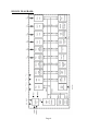
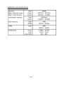
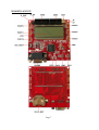
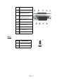
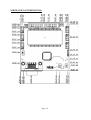
MOD-PULSE development board
Users Manual
All boards produced by Olimex are ROHS compliant
Revision Initial, March 2011
Copyright(c) 2011, OLIMEX Ltd, All rights reserved
Page 1
INTRODUCTION:
MOD-PULSE is an instrument for monitoring the blood oxygenation of a
human. By measuring the oxygen level and heart rate, MOD-PULSE can display the
levels of blood oxygenation and heart rate on it's LCD display. To perform it's functionality, MOD-PULSE requires external sensor connected to it via PROBE connector. MOD-PULSE can be connected to variety of OLIMEX's development boards via
it's UEXT connector.
BOARD FEATURES:
•
MCU: MSP430FG439
•
JTAG
•
UEXT
•
custom LCD
•
two user buttons
•
two status leds
•
power supply switch
•
+3V lithium battery connector
•
Battery connector for 2 x 1.5V AA batteries
•
DB9 – Female connector
•
System clock crystal
•
extension pin holes for each microcontroller's ports
•
FR-4, 1.5 mm, red soldermask, component print
•
Dimensions: 134.6x101.6mm (5.3 x 4.0")
ELECTROSTATIC WARNING:
The MOD-PULSE board is shipped in protective anti-static packaging. The board
must not be subject to high electrostatic potentials. General practice for working
with static sensitive devices should be applied when working with this board.
BOARD USE REQUIREMENTS:
Cables:
The cable you will need depends on the programmer/debugger
you use. If you use MSP430-JTAG-TINY, MSP430-JTAG-TINY-V2, or MSP430JTAG-ISO, you will need USB A-B cable. If you use MSP430-JTAG, you will need
LPT cable.
Page 2
Hardware:
Programmer/Debugger MSP430-JTAG, MSP430-JTAGTINY, MSP430-JTAG-TINY-V2, MSP430-JTAG-ISO, or other compatible
programming/debugging tool.
PROCESSOR FEATURES:
MOD-PULSE board uses ultralow power microcontroller MSP430FG439 from
Texas Instruments with these features:
−
Low Supply-Voltage Range, 1.8 V to 3.6 V
−
Ultralow-Power Consumption:
−
Active Mode: 300 μA at 1 MHz, 2.2 V
−
Standby Mode: 1.1 μA
−
Off Mode (RAM Retention): 0.1 μA
−
Five Power Saving Modes
−
Wake-Up From Standby Mode in Less Than 6 μs
−
16-Bit RISC Architecture, 125-ns Instruction Cycle Time
−
Single-Channel Internal DMA
−
12-Bit A/D Converter With Internal Reference, Sample-and-Hold and
Autoscan Feature
−
Three Configurable Operational Amplifiers
−
Dual 12-Bit D/A Converters With Synchronization
−
16-Bit Timer_A With Three Capture/Compare Registers
−
16-Bit Timer_B With Three Capture/Compare-With-Shadow Registers
−
On-Chip Comparator
−
Serial Communication Interface (USART), Select Asynchronous UART or
Synchronous SPI by Software
−
Brownout Detector
−
Supply Voltage Supervisor/Monitor With Programmable Level Detection
−
Bootstrap Loader
−
Serial Onboard Programming, No External Programming Voltage Needed
Programmable Code Protection by Security Fuse
−
Integrated LCD Driver for Up to 128 Segments
−
60KB+256B Flash Memory
−
2KB RAM
Page 3
BLOCK DIAGRAM:
Page 4
MEMORY ORGANIZATION:
Page 5
1
2
BH14S
JTAG
1
3
5
7
9
11
13
RST
TDO
TDI
TMS
TCK
1
5
2
6
3
B C817-40 SM D
OA0I0
P1.6
P1.5
P1.4
P1.3
P1.2
P1.1
P1.0
GND
TDO
TDI
TMS
TCK
RST
P6.0
P6.1
P6.2
GND
GND
AVCC
10uF/6.3V
1
2
3
61
62
63
64
65
66
67
68
69
70
71
72
73
74
75
76
77
78
79
80
P1.6/CA0
P1.5/TACLK/ACLK
P1.4/TBCLK/SMCLK
P1.3/TBOUTH/SVSOUT
P1.2/TA1
P1.1/TA0/MCLK
P1.0/TA0
XT2OUT
XT2IN
TDO/TDI
TDI
TMS
TCK
RST/NMI
P6.0/A0/OA0I0
P6.1/A1/OA0O
P6.2/A2/OA0I1
AVSS
DVSS1
AVCC
3V-LI_BAT+ -BC-20 01
+
Page 6
GND
P3.3/UCLK0/S28
P3.4/S27
P3.5/S26
P3.6/S25/DMAE0
P3.7/S24
S23
S22
S21
S20
P2.6/CAOUT/S19
P2.7/ADC12CLK/S18
S17
S16
S15
S14
S13
S12
S11
S10
P4.0/S9
NA
1
2
3
4
REF
R12
VEREF+
VREF+
VEREF-
NA
VCC
40
39
38
37
36
35
34
33
32
31
30
29
28
27
26
25
24
23
22
21
10uF/6.3V
C12
P1.7
1
NA
2
NA
3
680k
150k
R33
R13
CO M2
S0
4
R11
R26
5
45
C10
6
44
C9
7
43
32768Hz/6pF
8
6
4
2
P3.4
8
6
4
2
9
P3.7
P3.5
UCLK0
SIMO 0
P3.5
10
R10
680k
P3.6
11
680k
P3.7
12
R9
13
37
100nF
36
S2
NA(HN2X4)
7
5
3
1
PO RT5
NA(HN2X4)
R23
COM3
CO M1
S1
8
6
4
2
8
6
4
2
S19
UTXD0
P2.2
P2.0
S3
S5
S7
S9
P6.6
P6.4
P6.2
P6.0
NA(HN2X4)
7
5
3
1
PO RT6
NA(HN2X4)
7
5
3
1
d
g
a
c
b
C18 100nF
UCLK0
P3.4
P3.5
P3.6
P3.7
S23
S22
S21
S20
S19
S18
S17
S16
S15
S14
S13
S12
S11
S10
S9
http://www.olimex.com/dev
CO PYRIGHT(C) 2011, O LIMEX Ltd.
Rev. B
MOD-PULSE
P6.7
P6.5
P6.3
P6.1
S2
S4
S6
S8
7
5
3
1
PO RT2
PORT4
7
5
3
1
P3.6
P3.4
SO MI0
P3.0
8
6
4
2
NA(HN2X4)
S18
URXD0
P2.3
P2.1
PORT3
P1.6
P1.4
P1.2
P1.0
NA(HN2X4)
7
5
3
1
Extensions
S3
NA(0R) 38
R28
39
PO RT1
S22
S23
C11
8
42
8
6
4
2
14
P1.7
P1.5
P1.3
P1.1
15
35
100k
100k
S21
34
R7
R8
S20
Q1
P1.7
P2.0
P2.1
P2.2
P2.3
UTXD0
URXD0
G ND
VCC
R33
R23
R13
R03
COM3
CO M2
CO M1
CO M0
P3.0
SIMO 0
SO MI0
16
MSP430FG 439
60
59
58
57
56
55
54
53
52
51
50
49
48
47
46
45
44
43
42
41
33
U1
P1.7/CA1
P2.0/TA2
P2.1/TB0
P2.2/TB1
P2.3/TB2
P2.4/UTXD0
P2.5/URXD0
DVSS2
DVCC2
P5.7/R33
P5.6/R23
P5.5/R13
R03
P5.4/COM3
P5.3/COM2
P5.2/COM1
COM0
P3.0/STE0/S31
P3.1/SIMO0/S30
P3.2/SOMI0/S29
S9
S10
S11
DVCC1
P6.3/A3/OA1I1/OA1O
P6.4/A4/OA1I0
P6.5/A5/OA2I1/OA2O
P6.6/A6/DAC0/OA2I0
P6.7/A7/DAC1/SVSIN
VREF+
XIN
XOUT
VEREF+/DAC0
VREF-/VEREFP5.1/S0/A12/DAC1
P5.0/S1/A13
P4.7/S2/A14
P4.6/S3/A15
P4.5/S4
P4.4/S5
P4.3/S6
P4.2/S7
P4.1/S8
S19
17
LCD
S18
18
SW 2
41
S1
R29
4.7k
S17
19
T1107A(6x3.8x2.5mm)
LCD
R27
S0
OLIMEX_LTD
S16
20
C8
100nF
6
4
S15
21
C7
NA
5
S14
22
T1107A(6x3.8x2.5mm)
SW 1
VCC
OLIMEX
e
24
C6
100nF
4
1
2
3
4
5
6
7
8
9
10
11
12
13
14
15
16
17
18
19
20
2
VCC
P6.3
P6.4
P6.5
P6.6
P6.7
VREF+
XIN
XO UT
VEREF+
VEREFS0
S1
S2
S3
S4
S5
S6
S7
S8
C22
10uF/6.3V
NA(0R)
NA(0R) 40
0R
23
C5
100nF
0R
48
IS-1390(Default: UEXT is closed)
R42
47
COM2
COM3
GYX-SD-TC0805SURK(RED)
COM1
W F2S
C4
46
100nF
COM0
umHF
0R
f
32
1k
R34
4.7k
VEREF+
31
S8
10nF
B C817-40 SM D
1k
R33
20R
T2
circuit
S7
R6
R5
R35
20R
T4
T1
30
LED2
R36
4.7k
P6.6
T3
Pulsoximeter measurement
S6
GYX-SD-TC0805SURK(RED)
LED1
VREF+
100k
R38
P6.2
O A0I1
DB9 BFR
R37
15k
6
7
8
9
G2
1
2
3
4
5
R32
10k
29
C3
C20
G1PRO BE
P6.0
P2.3
28
S5
C2
3
R31
10k
VCC
S4
1
2
P1.4
P1.5
SOMI0
SIMO0
UCLK0
P3.0
1
O A0O
3.3pF P6.1
P2.2
27
BAT
VCC
3
J2
1-2:Open; 2-3:Close
4.7k
470k
OA1O
150k P6.3
47pF
25
BAT/UEXT
1
J1
1-2:Open; 2-3:Close
C21
R41
OA1I0
P6.4 R40
R39
26
S12
VCC
R4
4.7k
UTXD0
URXD0
UEXT
S13
3.3V_UEXT
BH10S
R3
4.7k
3.3V_UEXT VCC VCC
UEXT-1
UEXT-2
UEXT-3
UEXT-4
UEXT-5
UEXT-6
UEXT-7
UEXT-8
UEXT-9
UEXT-10
10k
R2
VCC
2
10nF
2
4
6
8
10
12
14
JTAG
BC80 7-40 SM D
C1
R1
100k
VCC
BC80 7-40 SM D
POWER SUPPLY
HN1x2(Close)
2
1
P_O UT
HN1x2(O pen)
P_IN
SCHEMATIC:
BOARD LAYOUT:
Page 7
POWER SUPPLY CIRCUIT:
MOD-PULSE can take power from:
–UEXT connector, when BAT/UEXT switch is in position UEXT. In this case the
jumper P_OUT has to be closed.
–JTAG, when jumper P_IN is closed.
–+3V via BAT connector, when BAT/UEXT switch is in position BAT. In this case
the jumper P_OUT has to be closed.
–+3V lithium battery via 3V-LI_BAT connector, when BAT/UEXT switch is in
position BAT. In this case the jumper P_OUT has to be closed.
The programmed board power consumption is about 30 mA with all peripherals
enabled. So, we recommend you to supply the board via BAT connector instead of
3V-LI_BAT connector.
RESET CIRCUIT:
MOD-PULSE reset circuit includes R1 (100k), C1 (10nF), JTAG connector
pin 11 and MSP43FG439 pin 74 (RST/NMI).
CLOCK CIRCUIT:
Quartz crystal Q1 32.768 kHz is connected to MSP430FG439 pin 8 (XIN)
and pin 9 (XOUT).
JUMPER DESCRIPTION:
P_IN
When this jumper is closed, the board is power supplied by the
standard JTAG pin 2. This is only possible when the consumption of
the board is not very high which is typically the case with MSP430
microcontrollers. If this jumper is open the board should be power
supplied by another external source. This jumper and P_OUT should
always be reversely open/closed, i.e. if P_IN is closed, P_OUT should
be open and vice versa.
Default state is opened.
P_OUT
When this jumper is closed, the board is power supplied not by the
JTAG but from external source. Then the JTAG has to synchronize
with the working voltages which is done through this line. This is
especially important when debugging with JTAG. This jumper and
P_IN should always be reversely open/closed, i.e. if P_OUT is closed,
P_IN should be open and vice versa.
Default state is closed.
Page 8
J1
When jumper J1 is shorted in position 1-2, UEXT pin 3 is connected to
MSP430FG439 pin 55 (P2.4/UTXD0) – signal “UTXD0”. When jumper
J1 is shorted in position 2-3, UEXT pin 3 is connected to
MSP430FG439 pin 54 (P2.5/URXD0) – signal “URXD0”.
Default state is shorted in position 2-3.
J2
When jumper J2 is shorted in position 1-2, UEXT pin 4 is connected to
MSP430FG439 pin 54 (P2.5/URXD0) – signal “URXD0”. When
jumper
J2 is shorted in position 2-3, UEXT pin 4 is connected to
MSP430FG439 pin 55 (P2.4/UTXD0) – signal “UTXD0”.
Default state is shorted in position 2-3.
Depending on jumpers J1 and J2 configuration, the board can work in host, or in device mode.
The default state of J1 and J2 is for device mode (shorted in position 2-3).
INPUT/OUTPUT:
Status led with name LED1 (red) connected to MSP430FG439 pin 67 (P1.0/TA0).
Status led with name LED2 (red) connected to MSP430FG439 pin 65 (P1.2/TA1).
User button with name SW1 connected to MSP430FG439 pin 59 (P2.0/TA2).
User button with name SW2 connected to MSP430FG439 pin 58 (P2.1/TB0).
Power supply switch with name BAT/UEXT – when in position BAT – the board is
power supplied via +3V lithium battery, when is in position UEXT – the board is
connected to other board with UEXT and is power supplied by the other board via
UEXT connector.
LCD custom display.
Page 9
EXTERNAL CONNECTORS DESCRIPTION:
UEXT:
Pin #
Signal Name
1
VDD
2
GND
3
TX
4
RX
5
P1.4
6
P1.5
7
SOMI0
8
SIMO0
9
UCLK0
10
P3.0
JTAG:
Pin #
Signal Name
Pin #
Signal Name
1
TDO
2
Via P_IN to VCC
3
TDI
4
Via P_OUT to VCC
5
TMS
6
Not Connected
7
TCK
8
Not Connected
Page 10
9
GND
10
Not Connected
11
RST
12
Not Connected
13
Not Connected
14
Not Connected
PORT1:
Pin #
Signal Name
Pin #
Signal Name
1
P1.0
2
P1.1
3
P1.2
4
P1.3
5
P1.4
6
P1.5
7
P1.6
8
P1.7
PORT2:
Pin #
Signal Name
Pin #
Signal Name
1
P2.0
2
P2.1
3
P2.2
4
P2.3
5
UTXD0
6
URXD0
7
S19
8
S18
PORT3:
Pin #
Signal Name
Pin #
Signal Name
1
P3.0
2
SIMO0
3
SOMI0
4
UCLK0
5
P3.4
6
P3.5
7
P3.6
8
P3.7
Page 11
PORT4:
Pin #
Signal Name
Pin #
Signal Name
1
S9
2
S8
3
S7
4
S6
5
S5
6
S4
7
S3
8
S2
PORT5:
Pin #
Signal Name
Pin #
Signal Name
1
S1
2
S0
3
COM1
4
COM2
5
COM3
6
R13
7
R23
8
R33
PORT6:
Pin #
Signal Name
Pin #
Signal Name
1
P6.0
2
P61
3
P6.2
4
P6.3
5
P6.4
6
P6.5
7
P6.6
8
P6.7
REF:
Pin #
Signal Name
Pin #
Signal Name
1
VEREF+
2
VREF+
3
VEREF-
4
GND
PROBE:
Pin #
Signal Name
Page 12
1
Not Connected
2
Driving line for sensor's
infrared and red led
3
Driving line for sensor's
infrared and red led
4
Not Connected
5
P6.2
6
Not Connected
7
GND
8
Not Connected
9
P6.0
BAT:
Pin #
Signal Name
1
to BAT/UEXT switch
2
GND
Page 13
MECHANICAL DIMENSIONS:
Page 14
AVAILABLE DEMO SOFTWARE:
Demonstrates blood oxygenation and heart rate measurement. For this demo you
must connect sensor to MOD-PULSE's PROBE connector.
–MOD-PULSE_DemoSoft IAR for MSP v4.21
Page 15
ORDER CODE:
MOD-PULSE - assembled and tested board
How to order?
You can order to us directly or by any of our distributors.
Check our web www.olimex.com/dev for more info.
Revision history:
Board's revision:
Rev. B, June 2011
Manual's revision:
Rev. Initial, June 2011
Page 16
Disclaimer:
© 2011 Olimex Ltd. All rights reserved. Olimex®, logo and combinations thereof, are registered
trademarks of Olimex Ltd. Other terms and product names may be trademarks of others.
The information in this document is provided in connection with Olimex products. No license, express
or implied or otherwise, to any intellectual property right is granted by this document or in
connection with the sale of Olimex products.
Neither the whole nor any part of the information contained in or the product described in this
document may be adapted or reproduced in any material from except with the prior written
permission of the copyright holder.
The product described in this document is subject to continuous development and improvements. All
particulars of the product and its use contained in this document are given by OLIMEX in good faith.
However all warranties implied or expressed including but not limited to implied warranties of
merchantability or fitness for purpose are excluded.
This document is intended only to assist the reader in the use of the product. OLIMEX Ltd. shall not
be liable for any loss or damage arising from the use of any information in this document or any error
or omission in such information or any incorrect use of the product.
Page 17