1
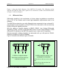
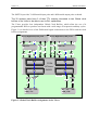
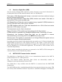
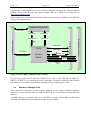
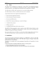
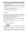
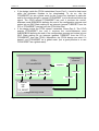
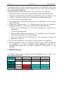
SMT338
User Manual
User Manual (QCF42); Version 3.0, 8/11/00; © Sundance Multiprocessor Technology Ltd. 1999
Version 1.5
Page 2 of 19
SMT338 User Manual
Revision History
Date
1 Oct
1999
2 Dec
1999
Comments
Engineer
E Puillet.
Initial Release
Modification of
Reconfiguration
the
FSM
for
the
FPGA E.Puillet
Version
Version1.0
Version1.1
06
Jan Clarification of the FSM and explanations for E.Puillet
2000
the FPGA Configuration and Reconfiguration.
Version
1.2
05.12.00
Description of the Installation and configuration E.Puillet
of the SMT338
Version
1.3
20.12.00
Addition of drawing for 50-way connector E.Puillet
pinout and of reference for mating 50-way
SCSI connector
Version
1.4
02.05.01
Modification of table 3 Pin out to match the E.Puillet
change of connector on the SMT338 (Female
to Male). Modification of explanations about
the reconfiguration in real time.
Version
1.5
31.03.04
Modification of paraghaph 3.1 section 3.1.1 E.Puillet
DONE is on LED 6
Version
1.6
This Document is intended only for the use of the individual or entity to which it is
addressed and contains information that is privileged and confidential. If the reader of
this message is not the intended recipient or the employee or agent responsible for
delivering the message to the recipient, you are hereby notified that any
dissemination, distribution or copying of this communication is strictly prohibited. If
you have received this communication in error, please notify sender immediately by
telephone and return the original message to sender. Thank you.
Version 1.5
Page 3 of 19
SMT338 User Manual
Table of Contents
Revision History.......................................................................................................... 2
Table of Contents ....................................................................................................... 3
List of Figures ............................................................................................................. 4
List of Tables .............................................................................................................. 4
Scope ......................................................................................................................... 4
1.
Technical description........................................................................................... 5
1.1.
Differential lines............................................................................................ 6
1.2.
Sundance Digital Bus (SDB) ........................................................................ 8
1.3.
SMT338-DSP Communication channels ...................................................... 8
1.4.
Sundance Datapipe Link .............................................................................. 9
1.5.
FPGA ......................................................................................................... 10
2.
Installation ......................................................................................................... 10
3.
Configuration ..................................................................................................... 11
3.1.
Hardware Sequence of events ................................................................... 11
3.1.1.
3.2.
At power-up......................................................................................... 11
FPGA Reconfiguration ............................................................................... 13
3.2.1.
Once configured.................................................................................. 13
3.3.
FPGA Reconfiguration in real time ............................................................. 13
3.4.
Software tools ............................................................................................ 14
4.
SMT338 Versions .............................................................................................. 15
5.
Interface ............................................................................................................ 16
Version 1.5
Page 4 of 19
SMT338 User Manual
List of Figures
Figure 1: SMT338 Block diagram ............................................................................................. 5
Figure 2: LVD Familly sets standard ........................................................................................ 6
Figure 3: Global Clock Buffers assignments in the Virtex ........................................................ 7
Figure 4: FPGA-DSP Communication Channels ...................................................................... 9
Figure 5: Global Reset routing. Use of FPGARESET as a global reset for designs............... 12
Figure 6: FPGA reconfiguration ............................................................................................. 13
Figure 7: SMT338 Layout ........................................................................................................ 16
Figure 8: SCSI Connector Front View (Male)......................................................................... 17
List of Tables
Table 1: Virtex-Differential I/Os Combinations ...................................................................... 15
Table 2: SMT338 connector reference table............................................................................ 16
Table 3: Differential Signals –50 WAY High-density cable Pins............................................. 17
Table 4: 40 Way SDB Connector Pins ..................................................................................... 18
Table 5: JTAG Connector ........................................................................................................ 19
Scope
This document describes the architecture, the function, the use and the interface
considerations for the SMT338. This document is intended for both the users of the SMT338
and the designer who is interested in designing the FPGA provided on the Board.
Version 1.5
Page 5 of 19
SMT338 User Manual
1. Technical description
50 way
Density
Diff_Con1
High
50 way
Density
Diff_Con2
High
Differential
Line converters
Differential
Line converters
DIFF1
DIFF2
Comm-Port
1,4,2,5
40
way
SDB_Con1
IDC
SDB 1
FPGA
Control
Bottom Primary
Connector
Global Bus
Connector
D[31:0]
XCVxxxxBG352-4
40
way
SDB_Con2
IDC
A[30:0]
SDB 2
IIOF2
Top Primary
Connector
H1
Comm-Port
50MHz Oscillator
Config Control
Comm-Port 3 Ctrl
Config D[7:0]
Comm-Port 3
Configuration Logic CPLD
Figure 1: SMT338 Block diagram
Comm-Port
Version 1.5
Page 6 of 19
SMT338 User Manual
Figure 1 shows the block diagram of the SMT338 I/O module. The following section
describes the SMT338 from a user’s point of view. Reference is made to the different blocks
of Figure 1 in the next Figures.
1.1.
Differential lines
Differential signalling is the mechanism of choice when long-distance connections
from a PC to the outside world or/and high bandwidth requirements need to be
satisfied.
The SMT338 provides the user with differential pairs connected to two on-board 50way headers on one end and to a Virtex FPGA on the other end to offer an extremely
flexible differential signalling solution.
With the ability to interface directly to RS422, RS485, Low Voltage Differential
Signalling (LVDS), and Bus LVDS (BLVDS) known as well under Multipoint LVDM
differential I/O standards, the SMT338 supports input, output and I/O signalling.
Point-to-point and multidrop transfers are achievable with up to 40 pairs for RS422,
RS485 at 32 Mbps or LVDS at 400Mbps.
Figure 2 describes the different types of transfer.
LVDM for multipoint buses.
More than one driver and one
receiver on the line
LVDS for point-to-point(1) and
multidrop(2) connections.
(1)One driver and one receiver on the
line
(2)One driver and more than one
receiver on the line.
Figure 2: LVD Familly sets standard
Version 1.5
Page 7 of 19
SMT338 User Manual
The SMT338 provides 32 differential input pairs and 8 differential output pairs on-board.
The 32 receiver pairs have 2 of their TTL outputs connected to two Global clock
buffers of the Virtex to be able to use its DLL capabilities.
The Virtex provides four independent Global Clock Buffers, which allow the use of 4
programmable DLLs to produce waveforms with a wide range of frequencies and duty cycles.
Figure 3 is a detailed view of the Differential signal connections to the FPGA and the clock
buffers assignments.
50 way High Density Diff_Con1
8
30
2
15
DIFF1
DIFF1
2
30
TTL
Diff Conv
4
50 way High Density Diff_Con2
Clk 1
Gnd
5
5
Gnd TTL
5
5
Diff Conv
15
Clk 2
DIFF2
1
BANK0
8
1
4
DIFF2
BANK1
FPGA
XCVxxxx
BG352
BANK5
BANK4
BoardClk
SDB A
Clk A
SDB B
Clk B
22
40
way
IDC
SDB_ConA
Figure 3: Global Clock Buffers assignments in the Virtex
22
40
way
IDC
SDB_ConB
Version 1.5
1.2.
Page 8 of 19
SMT338 User Manual
Sundance Digital Bus (SDB)
The four 40-way miniature IDC connectors’ primary function is to provide bi-directional 16bit data paths between TIMs with data transfer rates over 200 Mbytes/s.
Data rates of 200 Mbytes/second through a connector have been achieved using a
ground interlaced signal cable.
Each high speed Sundance Digital Bus (SDB) Interface can transfer 16-bit data, to
and from the TIM, at such a transfer rate.
400 Mbytes/Second Data rates can be reached using in parallel 2 (SDB) Interfaces to
send a 32-bit data every clock cycle at 100 MHz
The SDB Interface packs the 16-bit data transmitted into a 32-bit Word and stacks
them into a FIFO ready to be used.
The transmission can be fully bi-directional.
Many of Sundance TIM modules are being designed with this interface.
A SDB Interface is available from Sundance Multiprocessor Technology IP Centre.
Alternatively, the Sundance Digital Bus links can be extended to external
interconnection by connecting them to the SMT373 mezzanine card.
With this card, TTL signals are converted to Low-Voltage Differential signals and can
connect two systems several meters apart.
It provides two bi-directional 20-bit channels that can transfer up to 2 Gbytes/s through forty
SN65LVDM176 transceivers. Each channel provides 16 bit of data, a clock and a clockenable signal with their direction controlled by one signal. Two other signals can be used for
the bus arbitration in a bi-directional application. The direction of each of them can be
controlled independently.
All the signals controlling the direction are connected to the SMT338 FPGA through the
connectors and so can be controlled by software.
1.3.
SMT338-DSP Communication channels
The global bus or Comm-Port 0,1,2,34,5 or 6 are communication channels of the SMT338
used to interfaced to T.I.’s DSP processors.
The ‘C4x Protocol defines Byte-wide links which can theoretically transmit at
20Mbytes/second asynchronously between TIMs.
The Global Bus is only available when the SMT338 is connected onto the SMT350PB
motherboard.
The SMT350PB provides a non-blocking global bus interconnection between any source TIM
site and any other destination TIM site. It provides a sustainable throughput of 50 Mbytes/s
Version 1.5
Page 9 of 19
SMT338 User Manual
between any of the module sites even with three modules accessing the same destination
module. Access to the PCI bus takes place through TIM site 1. Please see our Web Site at
http://www.sundance.com/
Figure 4 shows the various dedicated DSP communication channels available on the SMT338
for inter-TIM data transfers.
Configuration Logic CPLD
Comm-Port 3
Config Control
Comm-Port 3
Global A[30:0]
FPGA
Global D[31:0]
Comm-Port 0
XCVxxxx
BG560
10
Global CTRL
H1
Bottom Primary Connector
8
4
Global Bus Connector
Top Primary Connector
Comm-Port 3 Ctrl
Config D[7:0]
IIOF2
Comm-Port
1245
Figure 4: FPGA-DSP Communication Channels
For developers who want to interface a SMT338 to a C4x or C6x TIM like the SMT302,
SMT331 or SMT332 via Comm-Ports or the Global Bus, a Comm-Port interface and a Global
Bus interface are available from Sundance Multiprocessor Technology IP Centre.
1.4.
Sundance Datapipe Link
The Comm-Port connections provided on the SMT338 can be used as Sundance Datapipe
Links for fast data transfers between SMT338-SMT338 or ‘C6x TIM based boards like the
SMT335.
An SDB interface is used and offers up to 100 MHz on copper and 50 MHz on flat-ribbon
cables like the FMS used on the Sundance range of carrier boards.
Version 1.5
1.5.
Page 10 of 19
SMT338 User Manual
FPGA
The FPGA is to be configured over Comm-Port 3 via the CPLD. The configuration bitstream
is sent by a ‘C6x or ‘C4x processor. This feature will allow a system to dynamically change
the FPGA firmware. The configuration LED indicates that configuration is complete.
The FPGA drives 4 LEDs, and is connected to it’s own local oscillator package.
The FPGA firmware will be user defined, and can be done on demand.
Typical functions that can be implemented in the FPGA are:
•
Full bi-directional global-bus interface
•
Full bi-directional Comm-Port interface
•
Bi-directional SDB Interface
•
RAM, FIFOs, Dual port RAMs up to a total of 16K Bytes
•
Communication protocols
•
DSP pre-processors
•
Any digital function that will fit in this size device
The SMT338 TIM can typically be used to interface with a SMT338 Frame Grabber over the
SDB connectors. The SMT338 can then perform customer specific data formatting before
sending it to a nearby C40 TIM via Comm-Port.
Due to the parallel nature of an FPGA it is well suited to handle multiple high-speed I/O lines.
The FPGA can then provide a cleaner bus-interface to the associated DSP processors.
2. Installation
The minimum system requirements needed to run a SMT338 on a PC is a C4x TIMbased carrier board and a C4x or C6x TIM with at least a Transmit Comm-Port
(Comm-Port 0,1 or 2) at Reset.
The goal is to connect one of the processors Comm-Port to Comm-Port 3 of the
SMT338.
Follow these steps to install the SMT338 module on a Host system:
1. Remove the carrier board from the host system.
2. Place the SMT338 module into one of the TIM sites on the carrier board.
Version 1.5
Page 11 of 19
SMT338 User Manual
3. Make sure the that the board is firmly seated, then provide the 3.3V to the board
by screwing the SMT338 on the two main mounting holes with the bolts and
screws provided with the board.
4. Fit the processor-based board on the carrier board. To do so, please follow the
installation procedure of that specific board. In the case of a SMT320 carrier
board, the C4x or C6x board MUST be placed on the first TIM slot (TIM slot 0) of
the SMT320.
5. Connect at least Comm-Port 3 of the SMT338 to one of the transmit Comm-Port
(at Reset) available on the Processor-based board.
6. Connect the SDB links as well if required by your application.
7. Replace the carrier board in the host system.
3. Configuration
The configuration of a SMT338 can only occur when a Global reset has been
asserted to the TIM. The carrier board on which the SMT338 TIM is plugged asserts
its Global Reset, often called TISRESET, at power up or when requested by any
software running on the host (Like Sundance 6000 Server).
The FPGA configuration is done by a software routine running on a host, or a ‘C6x or
‘C4x processor plugged on a carrier board root site.
The Virtex bitstream must be downloaded via Comm-Port 3 of the SMT338 which is
handled by theCPLD. After configuration, the CPLD gives the hand to the FPGA,
which becomes the owner of Comm-Port 3.
The CPLD does the handshake with the Comm-Port and communicates with the
FPGA as well.
The following description is referring to Figure 7.
3.1.
Hardware Sequence of events
3.1.1. At power-up.
1) The CPLD polls Comm-Port 3 until it receives the keyword 0xBCBCBCBC.
(WAITFORCMD State)
2) On receiving the start-of-bitstream keyword 0xBCBCBCBC, The CPLD reads out
the FPGA bitstream from Comm-Port 3 and configures the FPGA (CONFIG
State).
3) The FPGA releases its DONE pin when the configuration phase is finished. At
this time LED6 goes on (LED6 is directly driven by DONE). Then, the FPGA
completes its startup sequence and the design downloaded is now ready to start.
Version 1.5
Page 12 of 19
SMT338 User Manual
•
If the design inside the FPGA instantiates Comm-Port 3: it must be kept reset
while the bitstream finishes to be downloaded. To do so, use the
FPGARESET pin as a global reset for the Comm-Port interface in particular
and for the whole design in general. FPGARESET is a bi-directional active low
signal. The CPLD asserts FPGARESET low until it receives the end-ofbitstream word BCBCBC00 defining the end of the configuration process and
enters into an IDLE State waiting for an interrupt (general TISRESET from the
PCI or FPGARESET coming from the FPGA this time).
•
If the design inside the FPGA doesn’t instantiate Comm-Port 3: The CPLD
asserts FPGARESET low until it receives the end-of-bitstream word
0xBCBCBC00 defining the end of the configuration process and enters into an
IDLE State waiting for an interrupt (general TISRESET from the PCI or
FPGARESET from the FPGA). Meanwhile, the FPGA design can start if it
doesn’t use FPGARESET as a global reset. (but a good practice is to use
FPGA RESET as a global reset).
Top Primary
Connector
FPGA
XCVxxxxxBG352
Config Control
FPGARESET
Com-Port 3 Ctrl
Config D[7:0]
TIS_RESET
Com-Port 3
Com-Port 3 Data
TIS_RESET
FPGARESET
Logic
OR
TIS_RESET
Configuration Logic CPLD
Figure 5: Global Reset routing. Use of FPGARESET as a global reset for designs.
Version 1.5
3.2.
Page 13 of 19
SMT338 User Manual
FPGA Reconfiguration
The following description is referring to Figure 8.
3.2.1. Once configured.
When a TISRESET is received by the SMT338, the CPLD and the FPGA are reset.
4) The CPLD owns Comm-Port 3 and can configure the FPGA with a new bitstream
(repeat step 2).
5) The CPLD can leave Comm-Port 3 available to the FPGA and enter an Idle state
on receiving the command BCBCBC00.
Figure 6: FPGA reconfiguration
3.3.
FPGA Reconfiguration in real time
The SMT338 can be reprogrammed on-the fly by sending a new bitstream to the
Virtex FPGA.
It is possible to reconfigure the Virtex dynamically by sending a reconfigure
command to it.
The circuit recognizing a reconfiguration request must be implemented in the FPGA,
so any user-defined command can be sent over a Comm-port for instance.
An example design is provided in the software package for the SMT338 (SMT6338).
Version 1.5
Page 14 of 19
SMT338 User Manual
The design makes use of a Comm-port to pass the reconfigure command to the
SMT338 FPGA and waits for a 1 on the LSB of this Comm-Port.
If another Comm-port than Comm-port 3 is used, the pins corresponding to Commport 3 on the FPGA must be tied to “1” in the FPGA (As designed in the
reconfiguration example design)
The following description is referring to Figure 8.
6) The FPGA reads the command and then warns the CPLD by sending an interrupt
(FPGARESET low) that it decoded a reconfigure command. The FPGA goes into
a RESET state and leaves Comm-port 3 available for the CPLD. (in case Commport3 is used by the design).
7) On receiving the FPGARESET interrupt, the CPLD goes into the WAITCMD State
and polls Comm-port 3 for a keyword. (0xBCBCBCBC or 0xBCBCBC00)
8) On receiving the keyword,
•
If it is the end-of-bitstream keyword 0xBCBCBC00, the FPGA DOES NOT get
reconfigured, the CPLD leaves Comm-port 3 available for the FPGA and
enters into an IDLE state to wait for the next interrupt.
•
If it is the start-of-bitstream keyword 0xBCBCBCBC, repeat step 2 to 3).
3.4.
Software tools
The SMT6338 is a suite of software support for the SMT338.
It contains:
•
A library of IP cores: a Comm-port Interface and a SDB interface.
•
Design examples of Comm-Port and SDB applications.
•
The pin allocation file for the Virtex/E: VIRTEX_TOP.ucf.
•
The conversion software needed AFTER a bitstream has been generated to
format the bitstream.
Some additional software is required:
•
A CAD platform to create a schematic or VHDL design.
•
A simulator to simulate the hardware designs.
•
Xilinx Place & Route software such as M2.1i.
•
Texas Instrument C compiler or 3L parallel C compiler.
Version 1.5
Page 15 of 19
SMT338 User Manual
The bitstream that is used to configure the Virtex/E on the SMT338 is built using
Xilinx Design implementation tools for FPGAs such as M3.2i and the Sundance
conversion software bit2dat.exe.
Follow these steps to build a bistream that can be executed on the SMT338:
1. With the Xilinx tools, select your design available in edif format (filename.edf).
2. Target the constraint file provided with the SMT338 to map your design to the
Virtex/E ’s I/O pins (comment out all the I/Os that your design doesn’t use)
3. Run Xilinx Design implementation tools.
4. Next the bitstream is generated (Entityname.bit). The bitstream is a binary image
of the VHDL core.
5. Format the Entityname.bit to an Entityname.dat file with the standalone
application bit2dat.exe. To do so, you need to modify the Bit2dat.dat file.
•
Place the file Entityname.bit in the folder containing the executable file
Bit2dat.exe.
•
Edit the file Bit2dat.bat file.
•
Replace “bit2dat bitfilename bitfilename ” by “bit2dat Entityname Entityname”.
Note that the extension “.bit” is not necessary.
•
Save and double click the bit2dat.bat file. The executable is called and
generates a “.dat” file.
6. At this point the hardware core is ready for implementation in an application.
7. With an application running on the Processor-based board to which the SMT338
is connected to, or from a Windows based application, send the file
Entityname.dat through the Comm-port connected to Comm-Port3 on the
SMT338.
4. SMT338 Versions
The SMT338 comes under 2 standard versions, highlighted in red in Table 1. The
Virtex fitted is a XCV300-4.
SMT338
Virtex
XCV300
XCV 150
XCV 200
RS422
SMT338-422
SMT338-422
SMT338-422
RS644
SMT338-644
SMT338-644
SMT338-644
Differential
I/Os
Table 1: Virtex-Differential I/Os Combinations
Version 1.5
Page 16 of 19
SMT338 User Manual
5. Interface
P2
P2
CPLD
Voltage
Regulator
95144
SDB Conn2
SDB Conn1
Osc
VIRTEX FPGA
BG352
Driver
Receiver
Receiver
5 LE
DS
Driver
Receiver
Receiver
Receiver
J
T
A
G
DIFF2
Receiver
DIFF1
Receiver
50-way
high
density
connecto
r
Receiver
XCVxxx
50-way
high
density
connecto
r
JTAG Connector
P1
P1
Figure 7: SMT338 Layout
Table 2 shows the Physical Layout of the SMT338, indicating the external connectors with
their location and numbering.
Connector definitions are as follows:
SDB 1,2
DIFF1,
DIFF2
: Digital Data & Clock Input /Output Signal – Sundance Digital Bus High
Density ODU connector A (40-way High Density IDC Connectors).
Differential Signals –50 WAY SCSI Male connectors. Solder Pins.
JTAG
: JTAG Signals – 6-way connector.
P1
: Top Primary connector.
P2
: Bottom Connector. (Bottom Primary and Global Expansion Connectors)
Table 2: SMT338 connector reference table
Version 1.5
Page 17 of 19
Pin
SMT338 User Manual
Function
+, TTL and Ground
Pins
Drivers Pins
Receivers Pins
Ground Pins
1,26
TTL4/Gnd
2,27
TTL2/TTL3
3,28
TTL0/TTL1
4,29
Gnd/Gnd
5,30
Output Data 3
6,31
Output Data 2
7,32
Output Data 1
8,33
Output Data 0
9,34
Input Data 15
10,35
Input Data 14
11,36
Input Data 13
12,37
Input Data 12
13,38
Input Data 11
14,39
Input Data 10
15,40
Input Data 9
16,41
Input Data 8
17,42
Input Data 7
18,43
Input Data 6
19,44
Input Data 5
20,45
Input Data 4
21,46
Input Data 3
22,47
Input Data 2
23,48
Input Data 1
24,49
Input Data 0
25,50
Gnd/Gnd
Table 3: Differential Signals –50 WAY High-density cable Pins
1
25
26
50
Figure 8: SCSI Connector Front View (Male)
Version 1.5
Page 18 of 19
SMT338 User Manual
A mating connector can be found from HARTING.
The mating connector is a 50-way SCSI Female connector, solder cup.
The order code is 60 03 050 5180.
Function
Pin
Pin
Function
GND
2
1
CLK
GND
4
3
D0
GND
6
5
D1
GND
8
7
D2
GND
10
9
D3
GND
12
11
D4
GND
14
13
D5
GND
16
15
D6
GND
18
17
D7
GND
20
19
D8
GND
22
21
D9
GND
24
23
D10
GND
26
25
D11
GND
28
27
D12
GND
30
29
D13
GND
32
31
D14
GND
34
33
D15
CTRL1
36
35
USER_0
CTRL2
38
37
WEN
CTRL3
40
39
USER_1
Table 4: 40 Way SDB Connector Pins
Version 1.5
Page 19 of 19
Function
Pin
VCC
1
GND
2
TCK
3
TDO
4
TDI
5
TMS
6
Table 5: JTAG Connector
SMT338 User Manual