1
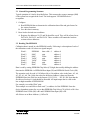
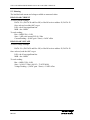
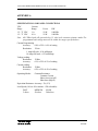
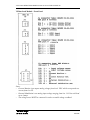
VXI LOAD OPERATIONS
MODELS 81201 & 81210
USER’S MANUAL
Part No. 09-0129
REVISION C
March 31, 1998
VXI LOAD OPERATIONS MODELS 81201 & 81210 USER’S MANUAL
Document History
Rev C
2 of 27
ECO 14612
3/31/98
B. H.
VXI LOAD OPERATIONS MODELS 81201 & 81210 USER’S MANUAL
Proprietary Rights Notice
This document and the information that it contains are the property of NH
Research, Incorporated. The rights to duplicate or otherwise copy this document,
the rights to disclose the document and its information to others, and the right to
use the information therein may be acquired only by written permission signed by a
duly authorized officer of NH Research, Incorporated.
Unauthorized duplication of software and documentation provided with the test
workstations violates the copyright protection provided by law. However, backup
copies of programs are permitted for archives and recovery from hardware failures.
The material in this publication is current as of the release date on the cover page
and is subject to change without notice. Any questions concerning the product or
any questions or comments concerning this manual should be directed to the NH
Research Field Service Department during normal business hours Monday through
Friday at (949) 474-3900 or FAX (949) 474-7062 or www.nhresearch.com.
POWERTEST and POWERFLEX are trademarks of NH Research, Incorporated.
3 of 27
VXI LOAD OPERATIONS MODELS 81201 & 81210 USER’S MANUAL
4 of 27
VXI LOAD OPERATIONS MODELS 81201 & 81210 USER’S MANUAL
TABLE OF CONTENTS
1. INTRODUCTION .............................................................................................................................. 7
2. OPERATIONAL THEORY............................................................................................................... 9
2.1 PROTECTION ....................................................................................................................................... 9
3. VXI LOAD PROGRAMMING SPECIFICATIONS....................................................................... 11
3.1 GENERAL PROGRAMMING STRUCTURE................................................................................................ 13
3.2 READING THE EEPROM.................................................................................................................... 13
4. OPERATING COMMANDS ........................................................................................................... 15
4.1 LOAD RESET...................................................................................................................................... 15
4.2 SET LOAD CURRENT .......................................................................................................................... 15
4.3 SET THE LOAD VOLTAGE ................................................................................................................... 15
4.4 SET THE LOAD OPERATING MODE ...................................................................................................... 16
4.5 MISCELLANEOUS FUNCTIONS ............................................................................................................. 16
5. READING AND METERING ......................................................................................................... 19
5.1 READING LOAD STATUS ..................................................................................................................... 19
5.2 READING THE ANALOG TO DIGITAL CONVERTER (ADC) ..................................................................... 19
5.3 METERING ........................................................................................................................................ 20
6. CALIBRATION ............................................................................................................................... 21
APPENDIX A ....................................................................................................................................... 23
SPECIFICATIONS AND PANEL CONNECTIONS .............................................................................. 23
APPENDIX B ....................................................................................................................................... 27
EEPROM TIMING DIAGRAMS ........................................................................................................... 27
5 of 27
VXI LOAD OPERATIONS MODELS 81201 & 81210 USER’S MANUAL
6 of 27
VXI LOAD OPERATIONS MODELS 81201 & 81210 USER’S MANUAL
1. INTRODUCTION
VXIbus electronic loads are designed for low-power output loading of DC power supplies
or other devices needing loads with either static or dynamic modes of operation. Each
load is a self-contained instrument on a single-slot, C-size VXlbus module making them
ideal for applications where size is important. The 81201 and 81210 can be integrated into
any VXlbus-based test system, but they are particularly well-suited to the POWERTEST
family of automatic power supply test systems from NH Research.
Although rated at 50 Watts continuous power, the 81201 and 81210 can be used at
considerably higher ratings. As most testing is carried out at substantially lower duty
cycles, analog control circuitry is used to continuously monitor internal conditions
permitting the load to increase its power handling capability with decreasing duty cycles.
Because the monitoring is carried out in real time, the protection circuitry is tripped only if
the load is in danger of being damaged. This allows testing for short periods or small duty
cycles at power levels in excess of the steady state specifications If higher power is
continuously required, two or more loads may be operated in parallel.
The 81201 and 81210 offer programmable transient response. Programmable rise times
permit the dynamic characteristics of the load to more closely approximate the operational
conditions in which the unit under test (UUT) will be expected to function. In applications
requiring testing under complex loading profiles, an analog input is provided which allows
external control of the load current over the load's full operating ranges. Using an arbitrary
waveform generator, virtually any required loading profile can be realized.
Frequently, switching power supplies must be turned on into a constant resistance load
before testing with a constant current load can begin. The 81201 and 81210 provide a
glitch-free transition from one mode to another; the supply under test does not see the
load current fall to zero during the mode transition. In the short circuit mode of operation,
an SCR in parallel with the shorting relay is used to give fast, low resistance short. It is
possible to shift from any mode to any other mode of operation under program control.
The loads are fully protected against various fault conditions including overvoltage,
reverse voltage, overcurrent, overpower and overtemperature. All calibration and
configuration data is stored in an on-board EEPROM, resulting in fast, internal “no pots"
calibration of setting and metering parameters. The result is a rugged, highly reliable load
that requires minimal maintenance.
7 of 27
VXI LOAD OPERATIONS MODELS 81201 & 81210 USER’S MANUAL
8 of 27
VXI LOAD OPERATIONS MODELS 81201 & 81210 USER’S MANUAL
2. OPERATIONAL THEORY
The VXlbus loads use power MOSFETs for the current sinking devices. The control
circuits are practically identical for both the 81201 and the 81210 loads. A few resistors
and a capacitor in the feedback are the differences (see page 3 of drawing 10-3860). A
control voltage is routed to the inverting input of an op-amp U9. The voltage developed
across the precision shunt is scaled and routed back into the op-amp. This op-amp drives
the gate of the MOSFET and will slew controlling the current until the error goes to zero.
The control voltage is programmed by the use of a 12 bit DAC U18. The stable voltage
reference for the DAC comes from U13. The DAC reference can come from 2 places, one
is the fixed reference, the other is derived from the constant resistance DAC U19. The
UUT voltage sensed by op-amp U1 is scaled such that full scale voltage represents 3.75
VDC. This voltage representing the UUT voltage is scaled for any nominal operating
voltage selected by DAC U19. Voltage references of both DAC U19 (Constant
Resistance) and DAC U18 (Constant Current) can be controlled by op-amp U1. This
method of controlling the reference allows the current of the load to be proportional to the
UUT voltage (i.e. constant resistance mode). Analog switch U16 controls the selection of
references and the mode of operation, Constant Resistance, or Constant Current. U16 also
controls slew rates by selecting between RC timing networks.
2.1 Protection
Temperature is sensed on the load heat sink by a temperature transducer. The output is
scaled by op-amp U15 and is compared to a stabilized reference. The output of the
transducer is also scaled by op-amp U8 and summed along with power multiplier U7.
Both outputs of the op-amps are ORed through diodes CR8 and CR9. If power is
exceeded or the temperature should rise above the preset value the load will be shut down
and a status bit will be available to the controller.
9 of 27
VXI LOAD OPERATIONS MODELS 81201 & 81210 USER’S MANUAL
10 of 27
VXI LOAD OPERATIONS MODELS 81201 & 81210 USER’S MANUAL
3. VXI LOAD PROGRAMMING SPECIFICATIONS
In general all addresses are offset values from the base load logical address as set be the
DIP switch, SW1.
SW1: open = 1, closed = 0
NUMBER
1
2
3
4
5
6
7
8
ADDRESS
A7
A6
A5
A4
A3
A2
A1
A0
For example, the logical address switch setting for 25(decimal) would look like:
1 2 3 4 5 6 7 8
X X
X
X X X
X X
open
closed
The remaining addresses listed are OFFSET values from the base address. Also, addresses
are HEX values, unless specified explicitly.
There are four (4) types of VXI load registers that begin at this Base address. Al1
addresses are 16 bits.
REGISTER
ID (read)
OFFSET
00
DEV-TYPE (read)
02
STATUS (read)
04
(write)
BIT DEFINITION
B0 - B11
: Manufacture ID
B12 - B13
: 00 (address space =
A16/24)
B14 - B15
: 11 (register based)
B0 - B11
: Model Code
B12 - B15
: 1110 (required memory)
B2
: 1 (self test passed)
B3
: 1 (self test extended)
B14
: MODID* self test extended
B15
: A24 active
B0
: Reset
B1
: Sysfail Inhibit - other bits
not used
B15
: A24 Enable
All device dependent registers begin at address 20 (HEX). There are 5 device write
registers and 3 device read registers.
11 of 27
VXI LOAD OPERATIONS MODELS 81201 & 81210 USER’S MANUAL
READ
ADDRESSES
Load Byte
OFFSET
20
Over
Load Byte
Load Byte
WRITE
ADDRESSES
Load Byte
24
26
OFFSET
20
Load Byte
22
Load Byte
24
Load Byte
(also all
26
Analog Switches
28
12 of 27
BIT DEFINITION
B0
EEPROM DATA IN/OUT
(SERIAL)
B1
SHORT CIRCUIT (also after an
Voltage)
B2
Power Limit (1=good, 0=bad)
B3
ADC STATUS(1=Converting,
0=done)
B4
OVER TEMPERATURE
B5 - B7
0
B0 - B7
ADC Lower 8 bits
B0 - B3
ADC Upper 4 bits
B4
ADC Overrange
B5
ADC Polarity
BIT DEFINITION
B0
EEPROM CHIP SELECT
B1
EEPROM SERIAL CLOCK
B2
EEPROM DATA INPUT
B3
SHORT CIRCUIT ON
B4
ADC RUN
B5
B6
OV RESET (also clears short
circuit)
B7
B0 - B3
Current DAC LSB's
B4 - B7
Voltage Scaling DAC LSB's
B0 - B7
Current DAC MSB's (also loads
LSB's)
B0 - B7
Voltage Scaling DAC MSB's
loads LSB's, Current and
Voltage)
B0 - B1
Mode Control
(10=Constant Resistance,
01 =Constant Current)
B2 - B3
Slew Rate Control
(10=slow, 01=medium, 11=high)
B4
not used
B5
Current Metering
B6
Voltage Metering
B7
Temperature Metering
VXI LOAD OPERATIONS MODELS 81201 & 81210 USER’S MANUAL
3.1 General Programming Structure
Typical operation of a load is described below. This assumes the resource manager (RM)
of the system has recognized the Load. The load supports VXI MODID device
recognition.
1. Configure
A. Read EEPROM data to determine the calibration data offset and gain factors for
the various functions.
B. Save this data in memory.
2. Reset load to desired start conditions
A. Registers for addresses 20, 22 and 28 should be saved. They will be referred to as
DATA 20, DATA 22, and DATA 28. These variables will contain the last data
written to these addresses.
3.2 Reading The EEPROM
Calibration data is stored in a the EEPROM serially. Following is a description of each of
the calibration words. All values are signed integers.
Word 1
Word 2
Word 3
Word 4
Word 5
Word 6
Word 7
EEPROM
IADC
IADC
VADC
VADC
IDAC
IDAC
data valid = 1
gain
offset
gain
offset
gain
offset
address 0
address 1
address 2
address 3
address 4
address 5
address 6
Data is read by setting EEPROM-Chip Select (CS) high, then serially shifting the address
data into the EEPROM via EEPROM-Data Input (Dl) and EEPROM-Serial Clock (SK).
The operation code for read is 110 followed by a 6 bit address value in the form: A5, A4,
A3, A2, A1, A0. The 16 bit data value for the desired address is then read from the
EEPROM-Data Out (DO) line in the format: 0, D15, D14,. . . D2, D1, D0. Note that the
first bit read is always 0, and should be discarded. All input/output data is valid on the
low-to-high transition of EEPROM-SK.
For example, to read the IDAC gain:
This example we would like to read word 7, or address 6 of the EEPROM. From the
device dependent register list we see that EEPROM-Chip Select (CS) is Bit 0 or B0. Also
EEPROM-Serial Clock (SK) is B1 and EEPROM-Data Input (Dl) is B2.
All of these are at Base Address (+) Offset 20.
13 of 27
VXI LOAD OPERATIONS MODELS 81201 & 81210 USER’S MANUAL
B2 B1 B0
Write to address 20 - data = 1 0
0
1
an instruction pending
Write to address 20 - data = 3 0
1
1
clock in pending instruction
Write to address 20 - data = 5 1
0
1
clock low, first bit of read op-code (110)
Write to address 20 - data = 7 1
1
1
clock in read command
Write to address 20 - data = 5 1
0
1
clock low, second bit of read op-code
(110)
Write to address 20 - data = 7 1
1
1
clock in, second bit of read op-code
Write to address 20 - data = 1 0
0
1
clock low, last bit of read op-code (110).
Write to address 20 - data = 3 0
1
1
clock in, last bit of read op-code.
The EEPROM now needs the Address. Address 6 = 0 0 0 1 1 0.
For each 0, write 1, followed by 3.
For each 1, write 5, followed by 7.
Now that the command and address have been set, reading address 20 should have B0 and
B1 both 0 (zero). This is the data start bit, and should be discarded.
For each bit of data: Write a 1, followed by a 3 (clock low to high) and then read the data
bit on the EEPROM Data Output (DO) line. This must be done 16 times in order to read
the entire 16 bit value. Please see timing diagram in appendix B.
Offset and Gain are divided by 10000 (decimal) to convert from integer to floating point
values.
Set Current offset:
Set Current gain:
Read Current Offset:
Read Current Gain:
Read Voltage Offset:
Read Voltage Gain:
IDAC OFFSET/10000
IDAC GAIN/10000
IADC OFFSET/10000
IADC GAIN/10000
VADC OFFSET/10000
VADC GAIN/10000
Note: Some offset factors may be large (i.e., in the 65000 range). These are actually
small negative number because the MSB (sign bit) implies an negative value.
The EEPROM should only be read once. The gain and offset factors saved in memory for
later usage. These numbers must be stored in standard 8088 16 bit Integer format, with
the 8 LSB at Varptr + 0 and 8 MSB at Varptr + 1.
14 of 27
VXI LOAD OPERATIONS MODELS 81201 & 81210 USER’S MANUAL
4. OPERATING COMMANDS
4.1 Load Reset
To reset the load the following steps must be taken:
1.
2.
3.
4.
Set the load current to zero (0).
Set the load mode to constant current.
Turn off the meter bus.
Pulse the over-voltage reset line.
4.2 Set Load Current
This function sets the current drawn by the load and requires two writes to the load.
Assume AMPS is the current to be set. To calculate what bits to write to the load scaling
must be done. Multiply the desired current by the IDAC gain previously extracted from
the EEPROM. Add the IDAC offset. Divide by the full scale current (81201 = 1 Amp and
81210 = 10 Amps) and multiply by 4095.
Scaled AMPS = (AMPS * IDAC gain) + IDAC offset
Bits to write = (Scaled AMPS/full scale current) * 4095
Calculate the most significant bits (MSB).
MSB = Bits to write\16 (integer divide to get 8 MSBs)
LSB = Bits to write and (HEX) OF (get 4 LSBs)
DATA 22 = (DATA 22 and (HEX)F0) or LSB (save the DATA 22 register)
write to device address 22, DATA 22
write to device address 24, MSB
4.3 Set the Load Voltage
This command sets the nominal load voltage used for constant resistance mode. This
function requires two (2) writes.
Assume VOLTS is the nominal load voltage to be set.
Bits to write = (VOLTS/75)*4095 (scaled by full scale voltage)
MSB = Bits to write\16 (integer divide to get 8 MSB)
LSB = Bits to write and (HEX) OF (4 LSB)
DATA 22 = (DATA 22 and (HEX)OF) or (LSB*16)
(save the DATA 22 register)
write to device address 22, DATA 22
write to device address 26, MSB
15 of 27
VXI LOAD OPERATIONS MODELS 81201 & 81210 USER’S MANUAL
4.4 Set the Load Operating Mode
This function will set constant current or constant resistance operation.
CONSTANT CURRENT
DATA 28 = DATA 28 and Hex FC
write to device address 28, Hex FC
DATA 28 = DATA 28 or 1
write to device address 28, DATA 28
(save value of register 28)
(clear mode)
(Constant Current Mode)
(write to address CC Mode)
CONSTANT RESISTANCE
Same as above only Constant Resistance Mode is a 2.
DATA 28 = DATA 28 or 2.
Notes:
A nominal voltage value should already have written prior to setting CR mode.
The data written to address 28 should always have D0 or D1 set!
To read load voltage or operate in constant resistance mode, the sense inputs must be
connected.
SET THE LOAD SLEW RATES
There are 3 possible slew rate values.
Slow = Hex 8
Medium = Hex 4
Fast = Hex 0C
Define rate = appropriate Hex value
DATA 28 = DATA 28 and Hex F3
DATA 28 = DATA 28 or RATE
4.5 Miscellaneous Functions
SHORT THE LOAD
DATA 20 = DATA 20 or 8
write to device address 20, DATA 20
16 of 27
(clear slew registers)
(set desired rate)
write to device address 28, DATA 28
VXI LOAD OPERATIONS MODELS 81201 & 81210 USER’S MANUAL
UNSHORT THE LOAD OR RESET OVER-VOLTAGE LATCH
(DATA 20 and Hex F7) or Hex 40
write to device address 20, DATA 20
DATA 20 = DATA 20 and Hex BF
write to device address 20, DATA 20
17 of 27
VXI LOAD OPERATIONS MODELS 81201 & 81210 USER’S MANUAL
18 of 27
VXI LOAD OPERATIONS MODELS 81201 & 81210 USER’S MANUAL
5. READING AND METERING
5.1 Reading Load Status
Executing a read from device address 20 will return a value for load status. Only the 5
LSB are defined.
B0 = EEPROM - DO
Data line to read when reading EEPROM data.
B1 = Short relay on/off*
A high indicates that the short relay has been
activated
B2 = Normal/Power limit*
A low indicates the load is in power limit
B3 = ADC status converting/Done* A high indicates the ACD converter is running
B4 = 0vertemp/Normal*
A high indicates an overtemp condition
5.2 Reading the Analog to Digital Converter (ADC)
The following shows the type of algorithm required to control the ICL7109 ADC.
1. Select the load function to be read.
2. Set run/hold* line high
a. DATA 20 = DATA 20 or Hex 10 write to device address 20, DATA 20
3. Delay 10mS (at least)
4. Set run/hold* line low
a. DATA 20 = DATA 20 or Hex EF write to device address 20, DATA 20
5. Monitor the ADC status line until it goes low.
a. Read device address 20
b. If (data read and Hex 08) = 8 then keep reading this until it equals zero (0).
6. Read data
a. Read device address 24 to get 8 LSB
b. Read device address 26 to get 4 MSB
c. If the data read from address has bit 4 set, indicates and ADC overrange (data read
and Hex 10).
d. If (data read and Hex 20) = 0 then signal is negative.
7. Scale data depending on function being read and set proper polarity for reading.
For Voltage:
If (DATA and Hex 20) = 0 then the voltage is negative.
For Current:
If (DATA and Hex 20) = Hex 20 then the current is negative. There really is no such
thing as a negative current for this load, so this value should be returned as 0 amps.
19 of 27
VXI LOAD OPERATIONS MODELS 81201 & 81210 USER’S MANUAL
5.3 Metering
The load has both current and voltage available as measured values.
READ LOAD CURRENT
To select current readings:
DATA 28 = (DATA 28 and Hex OF) or Hex B0 write to address 28, DATA 28
Once selected, read the ADC to get:
LSB = the 8 least significant bits
MSB = the 4 MSB
To scale reading:
Bits = (MSB*256) + LSB
Store = (full scale current/3839.0) * Bits
Current Reading = (IADC gain * Store) + IADC offset
READ LOAD VOLTAGE
To select voltage readings:
DATA 28 = (DATA 28 and Hex OF) or Hex B0 write to address 28, DATA 28
Once selected, read the ADC to get:
LSB = the 8 least significant bits
MSB = the 4 MSB
To scale reading:
Bits = (MSB *256) +LSB
Store = (0.0195 * Bits) (0.0195 = 79.8525/4096)
Voltage Reading = (VADC gain * Store) + VADC offset
20 of 27
VXI LOAD OPERATIONS MODELS 81201 & 81210 USER’S MANUAL
6. CALIBRATION
All the Calibration data is stored on the EEPROM internal to the unit. This allows for a
software "no pots" calibration. Calibration data is stored in a the EEPROM serially.
Following is a description of each of the calibration words. All values are signed integers.
Word 1
Word 2
Word 3
Word 4
Word 5
Word 6
Word 7
EEPROM
IADC
IADC
VADC
VADC
IDAC
IDAC
data valid = 1
gain
offset
gain
offset
gain
offset
address 0
address 1
address 2
address 3
address 4
address 5
address 6
A precision shunt, a DC Supply and a DMM are needed to calibrate the load. Calibration
points are 10% and 90% of Full Scale Voltage and Current.
Calibration Equations are as follows: Gain = QC2 - X1)/(Y2 - Y1)
0ffset = ((Y2*X1 ) - (Y1 *X2))/(Y2 - Y1 )
IDAC: X1:
10% OF FULL SCALE CURRENT(1 AMP for model 81201 and 10
Amps for model 81210
X2:
90% OF FULL SCALE CURRENT
Y1:
READING OF SHUNT AT 10% SETTING
Y2:
READING OF SHUNT AT 90% SETTING
IADC X1:
READING OF SHUNT AT 10% SETTING
X2:
READING OF SHUNT AT 90% SETTING
Y1:
READING OF IADC AT 10% SETTING
Y2:
READING OF IADC AT 90% SETTING
VADC X1:
VOLTAGE READ AT 10% SETTING (DMM)
X2:
VOLTAGE READ AT 90% SETTING (DMM)
Y1:
VOLTAGE READ AT 10% SETTING (\/ADC)
Y2:
VOLTAGE READ AT 90% SETTING (VADC)
Calibration parameters should be multiplied by 10000 (decimal) to convert floating point
to integer value before writing to the EEPROM.
The registers in the EEPROM must be erased (all bits set to logical "1") before new data
can be written into the registers. Registers are erased by setting the EEPROM Chip-Select
(CS) high then serially shifting the operation code and address data into the EEPROM via
EEPROM Dl and EEPROM SK. (please refer to section 3.2 Reading the EEPROM).
21 of 27
VXI LOAD OPERATIONS MODELS 81201 & 81210 USER’S MANUAL
The operation code for read is 111 followed by a 6 bit address value in the form: A5, A4,
A3, A2, A1, AO. After the Erase instruction is loaded into the EEPROM, CS must be
pulled low. The falling edge of this signal initiates the self-timed programming cycle. If CS
is brought high after a minimum delay of 1us the DO pin will remain low as long as the
EEPROM is still in the programming mode, and the return of this signal to logical "1"
indicates the device is now ready for the next instruction.
After erasing the register, write the new calibration parameters. Data is written by setting
the EEPROM Chip-Select (CS) high then serially shifting the operation code and address
data into the EEPROM via EEPROM Dl and EEPROM SK. (please refer to section 3.2
Reading the EEPROM).
The operating code for a write is 101. The 16 bits of data must be loaded into the device
in the format D15, D14, . . ., D2, D1, DO. After the last bit of data is loaded CS must be
brought low before the next rising edge of the serial clock. The high to low transition of
CS will initiate a programming cycle to the register whose address was specified in the
write instruction. (Please refer to timing diagram Appendix B).
22 of 27
VXI LOAD OPERATIONS MODELS 81201 & 81210 USER’S MANUAL
APPENDIX A
SPECIFICATIONS AND PANEL CONNECTIONS
VDC
Range
Current
Range
Power
BW
1.5 - 75 VDC
1.5 - 75 VDC
1A
10 A
50 W
50 W
100 KHz
100 KHz
Note: All VXIbus loads will operate below 1.5 volts in the constant resistance mode. The
programmed load voltage must still be within the ranges specified above.
Current Programming
Accuracy:
0.4% of FS + 0.4% of setting
Resolution: 12 bits
1 Amp full scale - 0.26 milliAmps
10 Amps full scale - 0.52 milliAmps
Voltage reading:
Resolution:
Accuracy:
12 Bits
0.1% of FS +0.5% of reading
Current reading:
Resolution:
Accuracy:
12 Bits
0.2% of FS +0.4% of reading
Operating Modes:
Constant Resistance
Constant Current
Short circuit (on/off)
Shut down.(high Z)
Equivalent Resistance Accuracy: 2% (V/I)
Load Speed (10% to 90% risetime - SW selectable):
FAST
5 uSecs
MEDIUM
50 uSecs
SLOW
500 uSecs
23 of 27
VXI LOAD OPERATIONS MODELS 81201 & 81210 USER’S MANUAL
VXIbus Load Module - Front Panel
J1
J2
J3
J4
-
24 of 27
Auxillary
UUT Input
Over voltage power supply
Over voltage coil
VXI LOAD OPERATIONS MODELS 81201 & 81210 USER’S MANUAL
VXIbus Load Module - Front Panel
6300074
6300830
Notes:
− Current Monitor is an output analog voltage from 0 to 8 VDC which corresponds to a
current from 0 to FS.
− External Modulation is an analog-input voltage ranging from 0 to -10 Volts with load
set to 0 amps.
− The voltage sense MUST be connected in order to enable voltage readback.
25 of 27
VXI LOAD OPERATIONS MODELS 81201 & 81210 USER’S MANUAL
26 of 27
VXI LOAD OPERATIONS MODELS 81201 & 81210 USER’S MANUAL
APPENDIX B
EEPROM TIMING DIAGRAMS
27 of 27