1
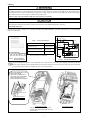
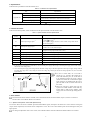
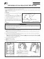
Instruction Manual
PG Interface (5 V Line Driver) Card "OPC-G1-PG2"
Thank you for purchasing this PG interface card or 5 V line driver card (hereinafter called PG interface card), "OPC-G1-PG2." Installing
this card to your FRENIC-MEGA enables vector control with speed sensor.
The FRENIC-MEGA has three option connection ports--A-, B-, and C-ports. Connect this PG interface card to the C-port. Do
not connect it to any other port.
1. Check that:
(1) A PG interface card and two screws (M3 8) are contained
in the package.
(2) The PG interface card is not damaged during
transportation--no defective devices, dents or warps.
(3) The model name "OPC-G1-PG2" is printed on the PG
interface card. (See Figure 1.)
Screw hole (left)
J1
If you suspect the product is not working properly or if you
have any questions about your product, contact the shop
where you bought the product or your local Fuji branch
office.
CN1
Release knob
Positioning cutout
Model name
Screw hole (right)
Figure 1 Front of Card
Figure 2
Back of Card
2. Installation
Before starting installation and wiring, turn OFF the power and wait at least five minutes for inverters with a capacity of 22 kW or
below, or at least ten minutes for inverters with a capacity of 30 kW or above. Make sure that the LED monitor and charging lamp are
turned OFF. Further, make sure, using a multimeter or a similar instrument, that the DC link bus voltage between the terminals P(+)
and N(-) has dropped to the safe level (+25 VDC or below).
Otherwise, electric shock could occur.
(1) Remove the front cover from the inverter and expose the control printed circuit board (control PCB). As shown in Figure 3, the
interface card can be connected to the C-port (CN6) only.
To remove the front cover, refer to the FRENIC-MEGA Instruction Manual, Section 2.3. For inverters with a capacity of 30 kW or
above, open also the keypad enclosure.
(2) Insert connector CN1 on the back of the PG interface card (Figure 2) into the C-port (CN6) on the inverter's control PCB. Then
tighten the two screws that come with the card. (Figure 4)
Check that the positioning cutout (Figure 1) is fitted on the tab ( in Figure 4) and connector CN1 is fully inserted ( in
Figure 4). Figure 5 shows the PG interface card correctly mounted. Do not connect the interface card to the ports other
than C-port. Doing so may damage the card.
(3) Perform wiring on the PG interface card.
Refer to Section 3 "Wiring."
(4) Put the front cover back into place.
To put back the front cover, refer to the FRENIC-MEGA Instruction Manual, Section 2.3. For inverters with a capacity of 30 kW or
above, close also the keypad enclosure.
Tab
Fit the positioning cutout of the card over the
tab on the inverter to determine the
mounting position.
Insert connector CN1 on the card into the
C-port (CN6) on the inverter's control PCB.
Figure 3
In the case of 0.4 kW
Figure 4
Mounting PG Interface Card
-1-
Figure 5
Mounting Completed
3. Wiring
In general, the covers of the control signal wires are not specifically designed to withstand a high voltage (i.e., reinforced insulation is
not applied). Therefore, if a control signal wire comes into direct contact with a live conductor of the main circuit, the insulation of the
cover might break down, which would expose the signal wire to a high voltage of the main circuit. Make sure that the control signal
wires will not come into contact with live conductors of the main circuit.
Failure to observe these precautions could cause electric shock or an accident.
Noise may be emitted from the inverter, motor and wires.
Take appropriate measures to prevent the nearby sensors and devices from malfunctioning due to such noise.
An accident could occur.
Perform wiring properly, referring to the "Terminal Allocation and Symbol Diagram," "Terminal Specifications," and "Internal Block
Diagram" shown below.
J1
PI EXT
Table 1
Terminal Specifications
Terminal Size
INT
+5 VDC
PO
M2
Tightening Torque
0.22 to 0.25 N·m
Recommended Wire Gauge *1
AWG16 to 24
Wire strip length
6 to 7 mm
*1 Insulated wires with allowable temperature of
105ºC (UL-listed) are recommended.
Figure 6 Terminal Allocation
and Symbol Diagram
Photocoupler
YA,YB,YZ
*YA,*YB,*YZ
I/F circuit
Photocoupler
CM
Wire break
detection circuit
Figure 7
Internal Block Diagram
To prevent malfunctioning due to noise, separate the wires for the interface card as far apart as possible from those for the main
circuits. Also, inside the inverter, bundle and fix the wires for the interface card so that they do not come into direct contact with
live parts of the main circuits (for example, the main circuit terminal block).
Connect the shielded layer of the
cable to terminal [CM].
When using an external power
supply, also connect its grounding
wire and shielded cable to this
terminal and tighten them together.
Connecting the cable to
terminals (magnified view)
In the case of 0.4 kW
Pass the wires from the PG interface card
between the control circuit terminal block and
the front cover.
-2-
In the case of 75 kW
4. Specifications
Table 2 lists the specifications of the PG interface card.
Table 2
PG Interface Card Specifications
Item
Applicable PG
Specifications
Pulse resolution
20 to 3000 P/R
Maximum response frequency
100 kHz
Pulse output system
Line driver (Equivalent to 26C31 or 26LS31)
Source current: +20 mA (max.), Sink current: -20 mA (max.)
Maximum wiring length
100 m (when using AWG16)
PG power supply *2
+5 VDC 10%, 200 mA or below
*2 If the PG current consumption exceeds 200 mA, use an external power supply.
5. Terminal Functions
Table 3 lists terminal symbols, names and functions of the option terminals on the PG interface card.
Table 3
Terminal
symbol
Option Terminals and Their Specifications
Name
Functions
PI
External power supply input *3
Power input terminal from the external device for the PG
+5 VDC 10% input *4
(Use the power supply 200 mA or above which is larger than the PG
current consumption.)
PO
Internal power supply output
Power output terminal for the PG
+5 VDC -0% to +10%, 200 mA output
CM
PG power common
Common terminal for power supply for PG
(Equipotent with [CM] terminal of the inverter)
YA
A(+) phase pulse input from slave PG
Input terminal for A(+) phase signal fed back from the slave PG
*YA
A(-) phase pulse input from slave PG
Input terminal for A(-) phase signal fed back from the slave PG
YB
B(+) phase pulse input from slave PG
Input terminal for B(+) phase signal fed back from the slave PG
*YB
B(-) phase pulse input from slave PG
Input terminal for B(-) phase signal fed back from the slave PG
YZ
Z(+) phase pulse input from slave PG
Input terminal for Z(+) phase signal fed back from the slave PG
*YZ
Z(-) phase pulse input from slave PG
Input terminal for Z(-) phase signal fed back from the slave PG
*3 If the PG current consumption exceeds 200 mA, use an external power supply. When using an external power supply, turn the slide switch J1
shown below to the EXT position.
*4 Use an external power supply whose rating meets the allowable voltage range of the PG. Regulate the external power supply voltage within the
PI voltage range (upper limit +10%), taking into account the voltage drop caused by the PG-inverter wiring impedance. Or, use a wire with a
larger diameter.
J1
• To move a switch slider, use a tool with a
narrow tip (e.g., tweezers). Be careful not to
touch other electronic parts, etc. If the slider is
in an ambiguous position, the circuit is unclear
whether it is turned ON or OFF and the digital
input remains in an undefined state. Be sure to
place the slider so that it contacts either side of
the switch.
SW1
SW1
• When not using the Z phase input, turn the
Z-phase wire break detection circuit OFF (by
turning SW1 to OFF, factory default); when
using it, turn the circuit ON (by turning SW1 to
ON).
6. Drive Control
For details of PG interface functions available, refer to the FRENIC-MEGA Instruction Manual, Chapter 5, Section 5.2 "Details of
Function Codes" or the FRENIC-MEGA User's Manual.
6-1. Speed control (Vector control with speed sensor)
The inverter detects the motor's rotational speed from PG feedback signals, decomposes the motor drive current into the exciting and
torque current components, and controls each of components in vector. The vector control enables speed control with high accuracy and
high response.
For settings and adjustments of the vector control, refer to FRENIC-MEGA Instruction Manual and FRENIC-MEGA User's Manual.
-3-
6-2. Control specifications
Table 4 lists the specifications of vector control with speed sensor.
Table 4 Specifications of Speed Control
Item
Control
specifications
Specifications
Remarks
Maximum output frequency
25 to 200 Hz *6
Speed control range
Minimum speed : Base speed = 1 : 1500
(For 4-pole motors: 1 to 1500 r/min)
Speed control accuracy
Analog setting: 0.2% or less of maximum frequency
(at 25 10 C)
Digital setting: 0.01% or less of maximum frequency
(at -10 to +50 C)
*5
When a PG with 1024 P/R
is connected.
*5 Specified values of the motor controllability will greatly vary depending on the pulse resolution, P/R. The recommended P/R is 1024 or more.
*6 If the output frequency exceeds 200 Hz, the inverter trips with the alarm
.
6-3. Connection diagram examples
Figure 8 shows the connection diagram example for speed control. Pulse train input to digital input terminal [X7] enables the inverter to
issue frequency commands.
When using inverter internal power supply
When using external power supply
FRENIC-MEGA
FRENIC-MEGA
L1/R
U
L1/R
L2/S
V
L3/T
W
M
U
L2/S
V
L3/T
W
OPC-G1-PG2
OPC-G1-PG2
*9 J1
*9 J1
EXT INT
EXT INT
PI
CM
*7
*7
YA
*YA
YB
*YB
YZ
*YZ
+5 VDC +- 10%
PI
CM
*7
PO
CM
YA
*YA
YB
*YB
YZ
*YZ
PO
CM
PG
*7
PG
*8
*8
Pulse train
generator
M
Pulse train
generator
X7 Control Circuit
CM
G
X7 Control Circuit
CM
G
*7 For wiring between the PG and the inverter, use a shielded cable. It is recommended that the shielded layer be open at the PG side and be
connected to the terminal [CM] on the PG interface card.
*8 If the wiring between the PG and the inverter is long, interference of A- and B-phases may cause PG signal malfunctions, resulting in
abnormal noise or torque pulsation. In such a case, minimizing the wiring length (by reviewing the wiring route) or using a cable with
smaller stray capacitance may reduce the problem.
*9 When using the inverter internal power supply, turn the slide switch J1 on the PG interface card to the INT position; when using an external
power supply, to the EXT position.
Figure 8 Connection Diagrams for Speed Control
Fuji Electric Co., Ltd.
Gate City Ohsaki, East Tower, 11-2, Osaki 1-chome, Shinagawa-ku, Tokyo 141-0032, Japan
URL http://www.fujielectric.com/
INR-SI47-1250b-JE
-4-