1
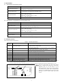
Instruction Manual PG Interface Card "OPC-G1-PG" Thank you for purchasing this PG interface card "OPC-G1-PG." Installing this card to your FRENIC-MEGA enables speed control with speed sensor and pulse train input. Installing this card disables pulse train inputs to the inverter's terminal [X7]. The FRENIC-MEGA has three option connection ports--A-, B-, and C-ports. Connect this PG interface card to the C-port. Do not connect it to any other port. 1. Check that: (1) A PG interface card and two screws (M3 × 8) are contained in the package. (2) The PG interface card is not damaged during transportation--no defective devices, dents or warps. (3) The model name "OPC-G1-PG/SY" is printed on the back of the PG interface card as shown in Figure 2. (The "PG/SY" on the front is a short name, as shown in Figure 1.) If you suspect the product is not working properly or if you have any questions about your product, contact the shop where you bought the product or your local Fuji branch office. Screw hole (left) Short name J1 Release knob Positioning cutout Figure 1 CN1 Model name Screw hole (right) Front of Card Figure 2 Back of Card 2. Installation Before starting installation and wiring, turn OFF the power and wait at least five minutes for inverters with a capacity of 22 kW or below, or at least ten minutes for inverters with a capacity of 30 kW or above. Make sure that the LED monitor and charging lamp are turned OFF. Further, make sure, using a multimeter or a similar instrument, that the DC link bus voltage between the terminals P(+) and N(-) has dropped to the safe level (+25 VDC or below). Otherwise, electric shock could occur. (1) Remove the front cover from the inverter and expose the control printed circuit board (control PCB). As shown in Figure 3, the PG interface card can be connected to the C-port (CN6) only. To remove the front cover, refer to the FRENIC-MEGA Instruction Manual, Section 2.3. For inverters with a capacity of 30 kW or above, open also the keypad enclosure. (2) Insert connector CN1 on the back of the PG interface card (Figure 2) into the C-port (CN6) on the inverter's control PCB. Then tighten the two screws that come with the card. (Figure 4) Check that the positioning cutout (Figure 1) is fitted on the tab ( in Figure 4) and connector CN1 is fully inserted ( in Figure 4). Figure 5 shows the PG interface card correctly mounted. Do not connect the PG interface card to the ports other than C-port. Doing so may damage the card. (3) Perform wiring on the PG interface card. Refer to Section 3 "Wiring." (4) Put the front cover back into place. To put back the front cover, refer to the FRENIC-MEGA Instruction Manual, Section 2.3. For inverters with a capacity of 30 kW or above, close also the keypad enclosure. Tab Fit the positioning cutout of the card over the tab on the inverter to determine the mounting position. Insert connector CN1 on the card into the C-port (CN6) on the inverter's control PCB. Figure 3 In the case of 0.4 kW Figure 4 Mounting PG Interface Card -1- Figure 5 Mounting Completed 3. Wiring In general, the covers of the control signal wires are not specifically designed to withstand a high voltage (i.e., reinforced insulation is not applied). Therefore, if a control signal wire comes into direct contact with a live conductor of the main circuit, the insulation of the cover might break down, which would expose the signal wire to a high voltage of the main circuit. Make sure that the control signal wires will not come into contact with live conductors of the main circuit. Failure to observe this precaution could cause electric shock or an accident. Noise may be emitted from the inverter, motor and wires. Take appropriate measures to prevent the nearby sensors and devices from malfunctioning due to such noise. An accident could occur. Perform wiring properly, referring to the "Terminal Allocation and Symbol Diagram," "Terminal Specifications," and "Internal Block Diagram" shown below. Table 1 Terminal Specifications PI EXT J1 SW1 INT PO PI PO PI YA PO YB XA YZ XB Terminal Size M2 Tightening Torque 0.22 to 0.25 N·m 12V 15V DC+15V DC+12V Optocoupler Recommended Wire Gauge* AWG16 to 26 XA,XB,XZ YA,YB,YZ Wire strip length 5 mm CM + CM XZ CM * Insulated wires with allowable temperature of 105ºC (UL-listed) are recommended. Figure 6 Terminal Allocation and Symbol Diagram Figure 7 Internal Block Diagram To prevent malfunctioning due to noise, separate the wires for the PG interface card as far apart as possible from those for the main circuits. Also, inside the inverter, bundle and fix the wires for the PG interface card so that they do not come into direct contact with live parts of the main circuits (for example, the main circuit terminal block). When grounding the shielded cable, use a crimp ring terminal, R1.25-3 or the like and fasten it together with the card using this screw. Location for grounding the shielded cable In the case of 0.4 kW Pass the wires from the PG interface card between the control circuit terminal block and the front cover. -2- In the case of 75 kW 4. Specifications 4-1. Specifications for pulse train inputs Item Specifications PG output pulse frequency 30 kHz max. (Open collector) 100 kHz max. (Complementary) PG pulse output circuit Open collector circuit (Maximum cable length: 20 m) Complementary circuit (Maximum cable length: 100 m) High level ≥ 8 VDC, Low level ≤ 3 VDC (For 12 VDC power supply) Input pulse threshold High level ≥ 10 VDC, Low level ≤ 3 VDC (For 15 VDC power supply) PG pulse input current 8 mA or less 4-2. Specifications of applicable PG and PG interface card Item Specifications Encoder pulse resolution 20 to 3000 P/R, A, B and Z phase pulse trains in incremental format Pulse output circuit Open collector (Maximum cable length: 20 m) Complementary (Maximum cable length: 100 m) High level ≥ 8 VDC, Low level ≤ 3 VDC (For 12 VDC power supply) Input power requirements High level ≥ 10 VDC, Low level ≤ 3 VDC (For 15 VDC power supply) Pulse output current 8 mA or less PG power supply* 12 VDC ±10%, 120 mA or less, or 15 VDC ±10%, 120 mA or less * If a power level required by the PG exceeds 120 mA, use an external power supply. 5. Terminal Functions Table 2 lists terminal specifications. Table 2 Terminal symbol Terminal Specifications Name Functions [P1] External power input*1 Connects external power supply for the PG. +12 VDC ±10% or +15 VDC ±10% (Use the power supply which is 150 mA more than PG current consumption.) [PO] Power output to the PG*2 Connects the PG power input. +12 VDC ±10%, 120 mA, or +15 VDC ±10%, 120 mA [CM] PG power common PG power common terminal (equipotent with [CM] terminal of the inverter) [XA] A phase pulse input from reference PG Input terminal for A phase signal fed back from the reference PG [XB] B phase pulse input from reference PG Input terminal for B phase signal fed back from the reference PG [XZ] Not used. [YA] A phase pulse input from slave PG Input terminal for A phase signal fed back from the slave PG [YB] B phase pulse input from slave PG Input terminal for B phase signal fed back from the slave PG [YZ] Z phase pulse input from slave PG Input terminal for Z phase signal fed back from the slave PG *1 Use an external power supply if the PG current consumption exceeds 120 mA. When using an external power supply, turn the slide switch J1 shown below to the EXT position. *2 Turn the internal switch (SW1) to the proper position according to the PG power requirement. The factory default position is "12V." J1 To move a switch slider, use a tool with a narrow tip (e.g., tweezers). Be careful not to touch other electronic parts, etc. If the slider is in an ambiguous position, the circuit is unclear whether it is turned ON or OFF and the digital input remains in an undefined state. Be sure to place the slider so that it contacts either side of the switch. SW1 SW1 15V INT 12V EXT -3- 6. Drive Control For details of PG interface functions available, refer to the FRENIC-MEGA Instruction Manual, Chapter 5, Section 5.2 "Details of Function Codes" or the FRENIC-MEGA User's Manual. 6-1. Pulse train input This function gives a frequency command to the inverter in pulse train format. Three types of formats are available--pulse train sign/pulse train input, run forward/run reverse pulse train, and 90 degree phase shifted A/B pulse trains. Use [XA] and [XB] terminals for the pulse train frequency command input. 6-1-1. Pulse train input format Table 3 lists pulse train input formats and operations of this option card. Table 3 Pulse Train Input Format and Operations Pulse input format Operations* Gives the speed command to the inverter, following the pulse input frequency on the [XB] terminal. Switching the terminal [XA] ON/OFF determines polarity of the speed command. Pulse train sign/pulse train input Gives the run forward speed command to the inverter, following the pulse input frequency on the [XB] terminal, if any. Run forward/run reverse pulse train Gives the run reverse speed command to the inverter, following the pulse input frequency on the [XA] terminal, if any. Gives the run forward or run reverse speed command to the inverter, following 90 degree phase shift and frequency information of two pulse inputs on [XA] and [XB] terminals. 90 degree phase shifted A/B pulse trains * Actual rotation direction of the motor is specified by a combination of the pulse input command polarity and FWD/REV command in the inverter. 6-1-2. Connection diagram examples Figure 8 shows the connection diagram example for pulse train input. When using pulse train generator When using PG FRENIC-MEGA FRENIC-MEGA L1/R U L1/R L2/S V L2/S V L3/T W L3/T W M U G G OPC-G1-PG OPC-G1-PG PI PO XA XB XZ CM PI *1 M *1 PO XA XB XZ CM Pulse train generator PG PO YA YB YZ CM PO YA YB YZ CM G G *1 For wiring between the encoder and the inverter, use a shielded cable. Basically, the shielded layer should be grounded. If any malfunction occurs due to noise, however, connecting the shielded layer to the terminal [CM] may reduce the problem. If the wiring between the encoder and the inverter is long, interference of A- and B-phases may cause encoder signal malfunctions, resulting in abnormal noise or torque pulsation. In such a case, minimizing the wiring length (by reviewing the wiring route) or using a cable with a smaller stray capacitance may reduce the problem. Figure 8 Connection Diagrams for Pulse Train Input -4- 6-2. Speed control (Vector control with speed sensor) The inverter detects the motor's rotational speed from PG feedback signals, decomposes the motor drive current into the exciting and torque current components, and controls each of components in vector. The vector control enables speed control with high accuracy and high response. (A recommended motor for this control is a Fuji VG motor exclusively designed for vector control.) For settings and adjustments of the vector control, refer to FRENIC-MEGA Instruction Manual and FRENIC-MEGA User's Manual. 6-2-1. Control specifications Table 4 lists the specifications of vector control with speed sensor. Table 4 Specifications of Speed Control Item Control specificatio ns *1 Specifications Remarks Maximum output frequency 25 to 200 Hz *2 Speed control range Minimum speed : Base speed = 1 : 1500 (For 4-pole motors: 1 to 1500 r/min) Speed control accuracy Analog setting: ±0.2% or less of maximum frequency (at 25 ±10°C) Digital setting: ±0.01% or less of maximum frequency (at -10 to +50°C) When a VG motor(1024 P/R) is connected. *1 Specified values of the motor controllability will greatly vary depending on the pulse resolution, P/R (Pulses/Revolution). The recommended P/R is 1024 or more. *2 If the output frequency exceeds 200 Hz, the inverter trips with the alarm 0s. 6-2-2. Connection diagram examples Figure 9 shows the connection diagram example for speed control. When using inverter internal power supply When using external power supply FRENIC-MEGA L1/R U L2/S V L3/T W FRENIC-MEGA U L1/R M L2/S V L3/T W G G OPC-G1-PG OPC-G1-PG J1 *5 EXT INT PI PO XA XB XZ CM PO YA YB YZ *2 CM J1 *5 EXT INT *3 *1 (PGP) (PA) (PB) (PGM) PI PO XA XB XZ CM M *3 PG *4 G G *1 (PGP) (PA) (PB) PO YA YB YZ *2 CM (PGM) PG *4 12 VDC ±10%/15 VDC ±10% *1 When a Fuji VG motor exclusively designed for vector control is connected, the signal names in parentheses ( ) apply. *2 The terminal [YZ] is not used for control. If the PG issues Z phase outputs, there is no need to connect the PG wire to this terminal. *3 For wiring between the PG and the inverter, use a shielded cable. Basically, the shielded layer should be grounded. If any malfunction occurs due to noise, however, connecting the shielded layer to the terminal [CM] may reduce the problem. If the wiring between the PG and the inverter is long, interference of A- and B-phases may cause PG signal malfunctions, resulting in abnormal noise or torque pulsation. In such a case, minimizing the wiring length (by reviewing the wiring route) or using a cable with a smaller stray capacitance may reduce the problem. *4 The terminal SS of the VG motor should be opened. *5 When using the inverter internal power supply, turn the slide switch J1 on the PG interface card to the INT position; when using an external power supply, to the EXT position. Figure 9 Connection Diagrams for Speed Control -5- Fuji Electric FA Components & Systems Co., Ltd. Mitsui Sumitomo Bank Ningyo-cho Bldg., 5-7, Nihonbashi, Odemma-cho, Chuo-ku, Tokyo, 103-0011, Japan Phone: +81 3 5847 8011 Fax: +81 3 5847 8172 URL: http://www.fujielectric.co.jp/fcs/ INR-SI47-1283-E -6-