1
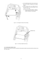
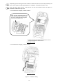
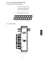
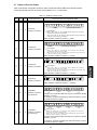
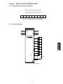
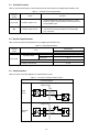
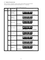
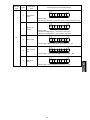
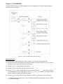
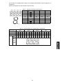
/ Instruction Manual
Digital Input Interface Card
"OPC-G1-DI"
Digital Output Interface Card
"OPC-G1-DO"
Fuji Electric Co., Ltd.
INR-SI47-1249c-JE
English Version
Preface
Thank you for purchasing our digital interface card(s).
This instruction manual describes the digital input interface card "OPC-G1-DI" and the digital output interface
card "OPC-G1-DO" designed for the FRENIC-MEGA series of inverters. For descriptions of the former, refer to
Chapter 2 "DIGITAL INPUT INTERFACE CARD"; for the latter, refer to Chapter 3 "DIGITAL OUTPUT
INTERFACE CARD." Chapters 1, 4, and 5 are common to both cards.
Mounting the digital input interface card on your FRENIC-MEGA makes it possible to specify frequency
commands with binary code (8, 12, 15, or 16 bits) or BCD (4-bit Binary Coded Decimal) code.
Mounting the digital output interface card on your FRENIC-MEGA enables monitoring with 8-bit binary code.
Each of the digital input interface card and the digital output interface card can be connected to any one of the
three option connection ports (A-, B-, and C-ports) on the FRENIC-MEGA. Concurrent use of both cards
provides a digital input/output interface.
This instruction manual does not contain inverter handling instructions. Read through this instruction manual in
conjunction with the FRENIC-MEGA Instruction Manual and be familiar with proper handling and operation of
this product. Improper handling might result in incorrect operation, a short life, or even a failure of this product.
Keep this manual in a safe place.
• Read through this instruction manual and be familiar with the digital interface card(s) before
proceeding with installation, connections (wiring), operation, or maintenance and inspection.
• Improper handling might result in incorrect operation, a short life, or even a failure of this product as
well as the motor.
• Deliver this manual to the end user of this product. Keep this manual in a safe place until this product
is discarded.
Safety precautions
Read this manual thoroughly before proceeding with installation, connections (wiring), operation, or
maintenance and inspection. Ensure you have sound knowledge of the device and familiarize yourself with all
safety information and precautions before proceeding to operate the inverter.
Safety precautions are classified into the following two categories in this manual.
Failure to heed the information indicated by this symbol may
lead to dangerous conditions, possibly resulting in death or
serious bodily injuries.
Failure to heed the information indicated by this symbol may
lead to dangerous conditions, possibly resulting in minor or
light bodily injuries and/or substantial property damage.
Failure to heed the information contained under the CAUTION title can also result in serious consequences.
These safety precautions are of utmost importance and must be observed at all times.
Installation and wiring
• Before starting installation and wiring, turn OFF the power and wait at least five minutes for inverters
with a capacity of 22 kW or below, or at least ten minutes for inverters with a capacity of 30 kW or
above. Make sure that the LED monitor and charging lamp are turned OFF. Further, make sure,
using a multimeter or a similar instrument, that the DC link bus voltage between the terminals P(+)
and N(-) has dropped to the safe level (+25 VDC or below).
• Qualified electricians should carry out wiring.
Otherwise, an electric shock could occur.
• Do not use the product that is damaged or lacking parts.
Doing so could cause a fire, an accident, or injuries.
• Prevent lint, paper fibers, sawdust, dust, metallic chips, or other foreign materials from getting into
the inverter and the option.
Otherwise, a fire or an accident might result.
• Incorrect handling in installation/removal jobs could cause a failure.
A failure might result.
• Noise may be emitted from the inverter, motor and wires. Implement appropriate measure to prevent
the nearby sensors and devices from malfunctioning due to such noise.
Otherwise, an accident could occur.
Operation
• Be sure to install the front cover before turning the inverter's power ON. Do not remove the cover
when the inverter power is ON.
Otherwise, an electric shock could occur.
• Do not operate switches with wet hands.
Doing so could cause an electric shock.
• If you configure the function codes wrongly or without completely understanding FRENIC-MEGA
Instruction Manual and the FRENIC-MEGA User's Manual, the motor may rotate with a torque or at a
speed not permitted for the machine. Confirm and adjust the setting of the function codes before
running the inverter.
Otherwise, an accident could occur.
Maintenance and inspection, and parts replacement
• Before proceeding to the maintenance/inspection jobs, turn OFF the power and wait at least five
minutes for inverters with a capacity of 22 kW or below, or at least ten minutes for inverters with a
capacity of 30 kW or above. Make sure that the LED monitor and charging lamp are turned OFF.
Further, make sure, using a multimeter or a similar instrument, that the DC link bus voltage between
the terminals P(+) and N(-) has dropped to the safe level (+25 VDC or below).
Otherwise, an electric shock could occur.
• Maintenance, inspection, and parts replacement should be made only by qualified persons.
• Take off the watch, rings and other metallic objects before starting work.
• Use insulated tools.
Otherwise, an electric shock or injuries could occur.
Disposal
• Treat the interface card(s) as an industrial waste when disposing of it.
Otherwise injuries could occur.
Others
• Never modify the interface card(s).
Doing so could cause an electric shock or injuries.
Icons
The following icons are used throughout this manual.
This icon indicates information which, if not heeded, can result in the product not operating to full
efficiency, as well as information concerning incorrect operations and settings which can result in
accidents.
This icon indicates information that can prove handy when performing certain settings or operations.
This icon indicates a reference to more detailed information.
Table of Contents
Preface ............................................................................... i
Safety precautions ............................................................. i
Chapter 1 BEFORE USING THIS OPTION .....................1-1
1.1 Acceptance Inspection ...........................................1-1
1.2 Applicable Inverters ................................................1-2
1.3 Operating Environment ..........................................1-2
1.4 Installation and Removal of the Interface Card.......1-2
1.4.1 Installing the interface card ............................1-3
1.4.2 Removing the interface card ..........................1-4
1.5 Wiring .....................................................................1-5
Chapter 2 DIGITAL INPUT INTERFACE CARD...............2-1
2.1 Terminal Allocation and Symbol Diagram .................2-1
2.2 Connection Diagram .................................................2-1
2.3 Terminal Functions .................................................2-2
2.4 Electrical Specifications ..........................................2-2
2.5 Input Interface ........................................................2-3
2.5.1 Switching between SINK and SOURCE
for digital input terminals ([I1] to [I16]) ...........2-3
2.5.2 Connection diagrams for SINK/SOURCE
input modes ...................................................2-3
2.5.3 Precaution on the use of a contact relay ........2-3
2.6 Configuring Inverter's Function Codes ...................2-4
2.7 Details of Function Codes ......................................2-5
Chapter 3 DIGITAL OUTPUT INTERFACE CARD...........3-1
3.1 Terminal Allocation and Symbol Diagram ...............3-1
3.2 Connection Diagram ...............................................3-1
3.3 Terminal Functions .................................................3-2
3.4 Electrical Specifications ..........................................3-2
3.5 Output Interface......................................................3-2
3.6 Configuring Inverter's Function Code .....................3-3
3.7 Details of Function Code ........................................3-4
Chapter 4 I/O CHECKING ...............................................4-1
Chapter 5 PROTECTIVE FUNCTION .............................5-1
Chapter 1
BEFORE USING THIS OPTION
1.1 Acceptance Inspection
Unpack the package and check the following:
(1) An interface card, two screws (M3 8), and the Digital Input Interface Card/Digital Output Interface Card
Instruction Manual (this manual) are contained in the package.
(2) The interface card is not damaged during transportation--no defective parts, dents or warps.
(3) The following model name is printed on the interface card.
• Digital input interface card: "OPC-G1-DI" (See Figure 1.1.)
• Digital output interface card: "OPC-G1-DO" (See Figure 1.2.)
If you suspect the product is not working properly or if you have any questions about your product, contact the
shop where you bought the product or your local Fuji branch office.
Screw hole (left)
Model name
Release knob
SW1
CN1
(Front)
Positioning cutout
(Back)
Screw hole (right)
Figure 1.1 Name of Parts on Digital Input Interface Card (OPC-G1-DI)
Screw hole (left)
Model name
Release knob
CN1
(Front)
Positioning cutout
(Back)
Screw hole (right)
Figure 1.2 Name of Parts on Digital Output Interface Card (OPC-G1-DO)
1-1
1.2 Applicable Inverters
This interface card is applicable to the following inverters and ROM version.
Table 1.1 Applicable inverter and ROM version
Series
Inverter type
FRENIC-MEGA
* The boxes
FRN
G1 -
Applicable motor rating
ROM version
All capacities
0500 or later
replace alphabetic letters depending on the nominal applied motor, enclosure, and power supply voltage.
To check the inverter's ROM version, use Menu #5 "Maintenance Information" on the keypad. (Refer to the
FRENIC-MEGA Instruction Manual, Chapter 3, Section 3.4.6 "Reading maintenance information."
Display on LED Monitor
Item
Inverter's ROM version
Description
Shows the inverter's ROM version as a 4-digit code.
1.3 Operating Environment
Install the inverter equipped with this interface card in an environment that satisfies the requirements listed in
Table 1.2.
Table 1.2 Environmental Requirements
Item
Specifications
Site location
Indoors
Surrounding temperature
Refer to the FRENIC-MEGA Instruction Manual, Chapter 2.
Relative humidity
5 to 95% (No condensation)
Atmosphere
The inverter must not be exposed to dust, direct sunlight, corrosive gases, flammable
gases, oil mist, vapor or water drops.
Pollution degree 2 (IEC60664-1) (Note)
The atmosphere can contain a small amount of salt.
(0.01 mg/cm2 or less per year)
The inverter must not be subjected to sudden changes in temperature that will
cause condensation to form.
Altitude
1,000 m max.
Atmospheric pressure
86 to 106 kPa
Vibration
Refer to the FRENIC-MEGA Instruction Manual, Chapter 2.
(Note) Do not install the inverter in an environment where it may be exposed to lint, cotton waste or moist dust or dirt which will
clog the heat sink of the inverter. If the inverter is to be used in such an environment, install it in a dustproof panel of your
system.
1.4 Installation and Removal of the Interface Card
Before starting installation and wiring, turn OFF the power and wait at least five minutes for inverters with a
capacity of 22 kW or below, or at least ten minutes for inverters with a capacity of 30 kW or above. Make
sure that the LED monitor and charging lamp are turned OFF. Further, make sure, using a multimeter or a
similar instrument, that the DC link bus voltage between the terminals P(+) and N(-) has dropped to the safe
level (+25 VDC or below).
Otherwise, an electric shock could occur.
1-2
• Do not use the product that is damaged or lacking parts.
Doing so could cause a fire, an accident, or injuries.
• Prevent lint, paper fibers, sawdust, dust, metallic chips, or other foreign materials from getting into
the inverter and the interface card.
Otherwise, a fire or an accident might result.
• Incorrect handling in installation/removal jobs could cause a failure.
A failure might result.
1.4.1 Installing the interface card
Before mounting the interface card, perform the wiring for the main circuit terminals and control circuit
terminals.
(1) Remove the front cover from the inverter and expose the control printed circuit board (control PCB). As
shown in Figure 1.3, the interface card can be connected to any one of the three option connection ports
(A-, B-, and C-ports) of the inverter.
To remove the front cover, refer to the FRENIC-MEGA Instruction Manual, Section 2.3. For inverters
with a capacity of 30 kW or above, open also the keypad enclosure.
(2) Insert connector CN1 on the back of the interface card (Figure 1.1 or 1.2) into any of the A-port (CN4),
B-port (CN5), and C-port (CN6) on the inverter's control PCB. Then tighten the two screws that come with
the card. (Figure 1.5)
Check that the positioning cutout (shown in Figures 1.1 and 1.2) is fitted on the tab ( in Figure 1.4)
and connector CN1 is fully inserted ( in Figure 1.4). Figure 1.5 shows the interface card correctly
mounted.
(3) Perform wiring on the interface card.
Refer to Section 1.5 "Wiring."
(4) Put the front cover back into place.
To put back the front cover, refer to the FRENIC-MEGA Instruction Manual, Section 2.3. For inverters
with a capacity of 30 kW or above, close also the keypad enclosure.
Figure 1.3 In the case of 0.4 kW
1-3
Fit the positioning cutout of the card over the
tab on the inverter to determine the mounting
position.
Insert connector CN1 on the card into any of
the three ports (A-, B- and C-ports) on the
inverter's control PCB.
Note: Be sure to follow the order of
and .
Inserting CN1 first may lead to insufficient
insertion, resulting in a contact failure.
Tab
Figure 1.4 Mounting the Interface Card (to B-port)
(Release knob)
Figure 1.5 Mounting Completed (to B-port)
1.4.2 Removing the interface card
Remove the two screws that secure the interface card and pull the release knob (shown above) to take the card
out of the inverter.
1-4
1.5 Wiring
• Before starting installation and wiring, turn OFF the power and wait at least five minutes for inverters with
a capacity of 22 kW or below, or at least ten minutes for inverters with a capacity of 30 kW or above.
Make sure that the LED monitor and charging lamp are turned OFF. Further, make sure, using a
multimeter or a similar instrument, that the DC link bus voltage between the terminals P(+) and N(-) has
dropped to the safe level (+25 VDC or below).
• Qualified electricians should carry out wiring.
Otherwise, an electric shock could occur.
• In general, the covers of the control signal wires are not specifically designed to withstand a high voltage
(i.e., reinforced insulation is not applied). Therefore, if a control signal wire comes into direct contact with
a live conductor of the main circuit, the insulation of the cover might break down, which would expose the
signal wire to a high voltage of the main circuit. Make sure that the control signal wires will not come into
contact with live conductors of the main circuit.
Failure to observe this precaution could cause an electric shock or an accident.
Noise may be emitted from the inverter, motor and wires.
Take appropriate measures to prevent the nearby sensors and devices from malfunctioning due to such
noise.
An accident could occur.
Perform wiring for the interface card observing the precautions below. Refer to the connection diagrams shown
in Figure 2.2 (Chapter 2) and Figure 3.2 (Chapter 3), and the wiring examples shown in Figure 1.8.
(1) Turn the inverter's power OFF.
(2) Use shielded wires.
(3) To prevent malfunction due to noise, keep the wiring for the interface card away from the main circuit wiring
and other power lines as far as possible. Never install them in the same wire duct.
(4) Complete wiring before turning the inverter ON.
(5) See Table 1.3 for the specifications of the terminal block on the interface card.
When using stripped wires (without attaching a crimp terminal), strip the wire end by 5 to 7 mm. (Figure 1.6)
When using a crimp terminal, attach a vinyl-insulated ferrule.
Loosen the terminal screw, insert the wire end into above the metal part of the terminal block, and tighten
the screw to fasten it. (Figure 1.7)
Table 1.3 Terminal Specifications
Item
Specifications
Wire size
AWG24 to AWG18 (0.25 to 0.75 mm2 ),
wire with rated temperature 105°C (UL) recommended
Terminal screw size
M2
Tightening torque
0.22 to 0.25 N·m
5 to 7 mm
Figure 1.6
Wire End Treatment (For Connection to
Terminals on Interface Card)
Figure 1.7
Connecting to a Terminal
on Interface Card
• Route the wiring of the interface circuit terminals as far from the wiring of the main circuit as
possible. Otherwise electric noise may cause malfunctions.
• Fix the interface circuit wires with a cable tie inside the inverter to keep them away from the live
parts of the main circuit (such as the terminal block of the main circuit).
1-5
Depending upon the wire type and the number of wires used, the front cover may be lifted by the
wires, which impedes normal keypad operation. If it happens, change the wire type or size.
Route the wires, taking care not to let them go over the control PCB, as shown in Figure 1.8.
Otherwise, malfunctions may occur.
• For inverters with a capacity of 22 kW or below
When grounding the shielded cable, use a
crimp ring terminal with insulation sheath,
R1.25-3 or the like and fasten it together
with the card using this screw.
* Pass the wires from the interface card between the control
circuit terminal block and the front cover.
In the case of 0.4 kW
• For inverters with a capacity of 30 kW or above
In the case of 75 kW
Figure 1.8 Examples of Wiring
1-6
Chapter 2
DIGITAL INPUT INTERFACE CARD
2.1 Terminal Allocation and Symbol Diagram
I16
CM
I15
I14
I12
I13
I10
I11
I8
I9
I6
I7
I4
I5
M1
I2
I3
I1
Figure 2.1 Terminal Allocation and Symbol Diagram
2.2 Connection Diagram
FRENIC-MEGA
L1/R
U
L2/S
V
L3/T
W
M1
OPC-G1-DI
I16
I15
I14
I13
I12
I11
I10
I9 SW1
I8
I7
I6
I5
I4
I3
I2
I1(LSB)
SINK
SOURCE
CM
Figure 2.2 Connection Diagram
2-1
2.3 Terminal Functions
Table 2.1 lists terminal symbols, names and functions of the terminals on the digital input interface card.
Table 2.1 Terminals and Their Specifications
Terminal
symbol
[I1] to [I16]
Name
Functions
(1) These digital inputs specify a frequency command
according to the settings made by function codes o19
and o20.
For details, refer to Section 2.6 "Configuring
Inverter's Function Codes."
Digital inputs 1 to 16
(2) SINK/SOURCE is switchable with the slide switch
SW1.
[M1]
External power supply input
Power input terminal from the external device for the
interface card (+22 to +27 VDC)
[CM]
Digital common
Common terminal for digital input signals
(Equipotent with [CM] terminal of the inverter)
2.4 Electrical Specifications
Table 2.2 lists the electrical specifications for the digital input interface card.
Table 2.2 Electrical Specifications
Terminal
symbol
[I1] to [I16]
Specifications
Item
Min.
Max.
Operating voltage
(SINK)
ON level
0V
2V
OFF level
22 V
27 V
Operating voltage
(SOURCE)
ON level
22 V
27 V
OFF level
0V
2V
2.5 mA
5 mA
-
0.5 mA
Operating current at ON
(Input voltage is at 0 V)
Allowable leakage current at OFF
2-2
2.5 Input Interface
2.5.1 Switching between SINK and SOURCE for digital input terminals ([I1] to [I16])
The input mode is switchable between SINK and SOURCE for digital input terminals ([I1] to [I16]) by using the
slide switch SW1 on the interface card (Figure 1.1 in Chapter 1). Specify the input mode referring to Table 2.3
below.
Table 2.3 Configuration of Slide Switch SW1
Input mode
Slide switch position
SINK
SW1
SINK (factory default)
SINK side
SOURCE
SW1
SOURCE
SINK
SOURCE side
SOURCE
The inverter also has the slide switch SW1 on the control PCB to specify SINK or SOURCE for the
inverter's digital input terminals. Match the setting of SW1 on the interface card with that of the
inverter.
2.5.2 Connection diagrams for SINK/SOURCE input modes
Table 2.4 shows connection diagrams for input interface circuits.
Table 2.4 Connections of Input Interface Circuits
Connection diagram
Power
supply
SINK mode
SOURCE mode
P L C *1
MEGA
In te rfa ce ca rd
M1
M1
Inte rfa ce ca rd
+ 24 V
+24 V
Internal
S IN K
S IN K
S O U RC E
S O U RC E
I1 to I1 6
I1 to I1 6
CM
CM
CM
CM
*1 The maximum allowable current for terminal
[PLC] on the FRENIC-MEGA is 100 mA.
Inte rface c ard
In te rface ca rd
M1
M1
+2 4 V
SI NK
External
SO UR CE
S O UR CE
+2 4 V I1 to I16
CM
+2 4 V
SIN K
+2 4 V I 1 to I1 6
CM
CM
2.5.3 Precaution on the use of a contact relay
To configure input circuits using contact relays, use highly reliable relays.
2-3
CM
2.6 Configuring Inverter's Function Codes
To enable frequency command inputs from this interface card, it is required to set function code data of F01
(Frequency Command 1) or C30 (Frequency Command 2) to "11" (Digital input interface card). Also specify the
polarity and input mode of the frequency command using function codes o19 (DI polarity) and o20 (DI mode)
provided for options, respectively.
Table 2.5 lists function codes and their parameters. The function codes o19 and o20 become available when the
digital input interface card is connected to the inverter.
Table 2.5 Function Codes and Parameters
Drive control *4
Function
code
F01
C30
Name
Frequency Command 1
Frequency Command 2
Data setting range
0:
/
keys on keypad
1:
Voltage input to terminal [12]
2:
Current input to terminal [C1]
3:
Sum of voltage and current inputs
to terminals [12] and [C1]
5:
Voltage input to terminal [V2]
7:
Terminal command UP/DOWN
control
8:
/
keys on keypad
(balanceless-bumpless switching
available)
V/f
w/o
PG
w/
PG
N
Y
0
Y
Y
Y
N
Y
0
Y
Y
Y
N
Y
0
Y
Y
Y
11: Digital input interface card
(option)
12: Pulse train input
o19
o20
DI option
0:
Without polarity
(DI polarity)
1:
With polarity *1
(DI mode)
0:
8-bit binary frequency command
1:
12-bit binary frequency command
2:
15-bit binary frequency command
3:
16-bit binary frequency command
4:
4-digit BCD frequency command
(0 to 99.99 Hz)
5:
4-digit BCD frequency command
(0 to 500.0 Hz)
BCD: Binary Coded Decimal
*1
*2
*3
*4
"Without polarity" when o20 = 4 or 5 (BCD).
Y: Possible, N: Impossible
Y: Possible, N: Impossible
Y: Applicable, N: Not applicable
For details, refer to the FRENIC-MEGA Instruction Manual.
2-4
2.7 Details of Function Codes
Table 2.6 shows the configuration of function codes o19 and o20 and the details of the terminal functions.
Turning the terminal input OFF or ON sets each bit data to "0" or "1," respectively.
Table 2.6 Details of Function Codes
No.
o19
o20
Input signal name
Terminal function and configuration details
MSB
I16 I15 I14 I13 I12 I11 I10
0
0
I9
I8
I6
I5
I4
I3
I2
I1
Frequency command
Invalid
8-bit binary
frequency command
LSB
I7
Hold signal
W hen I16 is OFF (0), the interface circuit updates the frequency
command according to the input data.
W hen I16 is ON (1), the interface circuit discards the input data and
holds the current frequency command.
Setting resolution = Maximum frequency
(1/255)
M SB
LS B
I16 I1 5 I1 4 I 13 I12 I1 1 I10
0
1
I8
I7
I6
I5
I4
I3
I2
H o ld sign al
W he n I1 6 is O FF (0), th e inte rface circuit up da tes th e freq uen cy
com m and accordin g to the inpu t data .
W he n I16 is O N (1), the interface circu it d iscard s th e inp ut data and
ho lds the cu rrent fre qu ency co m m and.
Setting resolution = Maximum frequency
(1/4095)
LS B
M SB
I16 I15 I 14 I 13 I12 I 11 I10
0
2
I9
I8
I7
I6
I5
I4
I3
I2
H o ld s ign a l
W h en I16 is O FF (0), th e inte rface circu it up da tes the frequ ency
com m an d accordin g to the inp ut data .
W h en I16 is O N (1), the in terfa ce circuit discards the inp ut data a nd
ho lds the current fre qu ency com m and .
(1/32767)
M SB
3
16-bit binary
frequency command
LS B
I16 I15 I14 I13 I1 2 I1 1 I1 0
I9
I8
I7
I6
I5
I4
I3
I2
I3
I2
(1/65535)
M SB
LS B
I16 I15 I14 I13 I1 2 I1 1 I1 0
0, 1
4
Te ns pla ce
of H z
I9
I8
I7
I6
I5
Te nth p lace
of H z
U nits pla ce
of H z
I4
H und red th p lace
of H z
M SB
LS B
H und red s place
of H z
5
4-digit BCD
frequency command
(0 to 500.0 Hz)
I1
Frequency can be specified within the range of 0 to 99.99 Hz (Setting
resolution = 0.01 Hz).
If a frequency command exceeding the maximum frequency is input,
the maximum frequency applies.
I16 I1 5 I1 4 I13 I12 I11 I10
0, 1
I1
F re qu e nc y c o m m a n d
Setting resolution = Maximum frequency
4-digit BCD
frequency command
(0 to 99.99 Hz)
I1
F re qu en c y c om m a nd
15-bit binary
frequency command
Setting resolution = Maximum frequency
0
I1
F re qu en c y c om m a nd
In valid
12-bit binary
frequency command
I9
Te ns pla ce
o f Hz
I9
I8
I7
I6
U nits pla ce
of H z
I5
I4
I3
I2
I1
Te nth p lace
o f Hz
H o ld s ig n al
W h en I16 is O F F (0 ), the inte rface circuit upd ate s th e freq uen cy
co m m a nd a ccordin g to the inp ut d ata.
W h en I16 is O N (1 ), the in terfa ce circuit discards the inpu t data a nd
h old s th e cu rre nt fre qu enc y com m an d.
Frequency can be specified within the range of 0 to 500.0 Hz. (Setting
resolution = 0.1 Hz).
If a frequency command exceeding the maximum frequency is input,
the maximum frequency applies.
2-5
No.
o19
o20
Input signal name
Terminal function and configuration details
M SB
I16 I1 5 I1 4 I13 I 12 I11 I1 0
I9
I8
LS B
I7
I6
I5
I4
I3
I2
I1
F re qu e nc y c o m m an d
Inv alid
H o ld sig na l
1
0
8-bit binary
frequency command
W h en I16 is O FF (0 ), the inte rface circuit u pd ate s the freq uen cy
com m an d a ccord ing to the inp ut d ata.
W h en I16 is O N (1), the in terface circuit disca rds the inp ut da ta a nd
ho lds th e curren t fre qu ency com m an d.
Frequency setting range:
-(Maximum frequency) to +(Maximum frequency)
= -128 to +127
Setting resolution = Maximum frequency x (1/127)
M SB
LS B
I16 I1 5 I1 4 I13 I 12 I11 I1 0
I9
I8
I7
I6
I5
I4
I3
I2
I1
F re qu e n cy c o m m a nd
In valid
H o ld sig na l
1
1
12-bit binary
frequency command
W h en I16 is O FF (0 ), the inte rface circuit u pd ate s the freq uen cy
com m an d a ccord in g to th e in pu t d ata.
W h en I16 is O N (1), the in terface circuit disca rds the inp ut da ta a nd
ho lds th e curren t fre qu ency com m an d.
Frequency setting range:
-(Maximum frequency) to +(Maximum frequency)
= -2048 to +2047
Setting resolution = Maximum frequency
(1/2047)
M SB
LS B
I1 6 I15 I1 4 I13 I12 I11 I1 0
I9
I8
I7
I6
I5
I4
I3
I2
I1
F re qu e nc y c o m m a nd
H o ld s ig n al
1
2
15-bit binary
frequency command
W h en I16 is O F F (0 ), the inte rface circuit u pd ate s the freq uen cy
co m m an d a ccord ing to the inp ut d ata.
W h en I16 is O N (1 ), the in terface circuit disca rds the inp ut data a nd
h old s th e cu rren t fre qu ency com m an d.
Frequency setting range:
-(Maximum frequency) to +(Maximum frequency)
= -16384 to +16383
Setting resolution = Maximum frequency
(1/16383)
M SB
LS B
I1 6 I15 I14 I1 3 I 12 I11 I 10
1
3
16-bit binary
frequency command
I9
I8
I7
I6
I5
I4
I3
F re qu e nc y c om m a nd
Frequency setting range:
-(Maximum frequency) to +(Maximum frequency)
= -32768 to +32767
Setting resolution = Maximum frequency
2-6
(1/32767)
I2
I1
Chapter 3
DIGITAL OUTPUT INTERFACE CARD
3.1 Terminal Allocation and Symbol Diagram
O8
O7
O6
O5
O4
O3
O2
O1
M2
Figure 3.1 Terminal Allocation and Symbol Diagram
3.2 Connection Diagram
FRENIC-MEGA
L1/R
U
L2/S
V
L3/T
W
OPC-G1-DO
Ry
(MSB) O8
Ry
O7
Ry
O6
Ry
O5
Ry
O4
Ry
O3
Ry
O2
Ry
(LSB) O1
24 VDC
CM
Figure 3.2 Connection Diagram
3-1
3.3 Terminal Functions
Table 3.1 lists terminal symbols, names and functions of the terminals on the digital output interface card.
Table 3.1 Terminals and Their Specifications
Terminal
symbol
[O1] to [O8]
Name
Functions
Transistor outputs 1 to 8
These digital terminals output various status (e.g., output
frequency, output current) specified by function code o21 as
an 8-bit parallel signal.
Common terminal for transistor output signals.
[M2]
Transistor output common
This terminal is electrically isolated from terminals [CM],
[11]s, and [CMY].
3.4 Electrical Specifications
Table 3.2 lists the electrical specifications for the digital output interface card.
Table 3.2 Electrical Specifications
Specifications
Terminal
symbol
Item
Max.
Operating voltage
[O1] to [O8]
ON level
2V
OFF level
27 V
Source current at ON
50 mA
Leakage current at OFF
0.1 mA
3.5 Output Interface
Table 3.3 shows connection diagrams for output interface circuits.
Table 3.3 Connections of Output Interface Circuits
Connection diagram
Interface card
M2
SINK
mode
O1 to O8
24 V
Interface card
M2
24 V
SOURCE
mode
O1 to O8
3-2
3.6 Configuring Inverter's Function Code
Function code o21 (DO mode selection) provided for options specifies the item to be monitored by digital signals
of this digital output interface card.
Table 3.4 lists the function code and its parameters. The function code o21 becomes available when the digital
output interface card is connected to the inverter.
Table 3.4 Function Code and Parameters
Drive control *3
Function
code
o21
Name
DO option
(DO mode selection)
Data setting range
0: Output frequency
(before slip compensation)
1: Output frequency
(after slip compensation)
2: Output current
3: Output voltage
4: Output torque
5: Load factor
6: Input power
7: PID feedback amount
8: PG feedback value
9: DC link bus voltage
13: Motor output
15: PID command (SV)
16: PID output (MV)
*1
*2
*3
Y: Possible, N: Impossible
Y: Possible, N: Impossible
Y: Applicable, N: Not applicable
For details, refer to the FRENIC-MEGA Instruction Manual.
3-3
Y
Y
0
V/f
w/o
PG
w/
PG
Y
Y
Y
3.7 Details of Function Code
Table 3.5 shows the configuration of function code o21 and the details of the terminal functions.
Turning the terminal output OFF or ON sets each bit data to "0" or "1," respectively.
Table 3.5 Details of Function Code
Function
code
Data
0
1
2
Output signal
name
Terminal function and configuration details
Output frequency
(before slip
compensation)
Terminal output = (Output frequency/Maximum frequency)
255
Terminal output = (Output frequency/Maximum frequency)
255
Output frequency
(after slip
compensation)
Output current
Terminal output
= (Output current/(Inverter rated output current x 2))
3
255
Output voltage
Terminal output =(Output voltage/250 V) 255, for 200 V class series
= (Output voltage/500 V) 255, for 400 V class series
o21
4
Output torque
Terminal output = (Output torque/(Motor rated torque x 2))
5
Load factor
Terminal output = (Load factor/(Motor rated load x 2))
6
255
Input power
Terminal output = (Input power/ (Inverter rated output x 2))
7
255
PID feedback
amount
Terminal output
= (PID feedback amount/100% of feedback amount)
3-4
255
255
Function
code
Data
8
Output signal
name
Terminal function and configuration details
PG feedback
value
Terminal output
= (PG feedback value/100% of synchronous speed at maximum frequency)
9
DC link bus
voltage
Terminal output
= (DC link bus voltage/500 V) 255, for 200 V class series
= (DC link bus voltage/1000 V) 255, for 400 V class series
o21
13
Motor output
Terminal output = (Motor output/(Motor rated output
15
2))
PID command
(SV)
Terminal output = (PID command/100% of feedback value)
16
255
PID output
(MV)
Terminal output = (PID output/Maximum frequency)
3-5
255
255
255
Chapter 4
I/O CHECKING
Using Menu #4 "I/O Checking" in FRENIC-MEGA program mode displays the I/O status of external signals on
the LED monitor of the keypad.
Figure 4.1 Menu Transition in Menu #4 "I/O Checking"
Basic key operation
To check the status of the I/O signals, set function code E52 to "2" (Full-menu mode) beforehand.
(1) Turn the inverter ON. It automatically enters Running mode. In that mode, press the
Programming mode. The function selection menu appears.
(2) Use the
(3) Press the
(4) Use the
and
keys to display "I/O Checking" (
).
keys to display "Option control circuit terminal (I/O)" (
The corresponding I/O check data appears. Using the
between the segment display and hexadecimal display.
(5) Press the
).
key to proceed to a list of I/O check items (e.g.
and
key to switch to
and
key to return to the list of I/O check items. Press the
), then press the
key.
keys switches the display method
key again to return to the menu.
For details of Menu #4 "I/O Checking," refer to the FRENIC-MEGA Instruction Manual, Chapter 3, Section
3.4 "Programming Mode."
4-1
The I/O status of the digital interface card(s) can be displayed with ON/OFF of the LED segment or in
hexadecimal.
Signals are assigned to the LED segments as shown below.
Table 4.1 Display with ON/OFF of LED Segments
Segment
LED3
LED2
LED1
a
b
c
LED4
O1
O2
O3
I9
I10
I11
I1
I2
I3
d
e
f
g
dp
O4
O5
O6
O7
O8
I12
I13
I14
I15
I16
I4
I5
I6
I7
I8
Table 4.2 Segment Display for I/O Signal Status in Hexadecimal
LED number
LED4
LED3
LED2
LED1
Bit
15
14
13
12
11
10
9
8
7
6
5
4
3
2
1
0
Input terminal
I16
I15
I14
I13
I12
I11
I10
I9
I8
I7
I6
I5
I4
I3
I2
I1
Output terminal
-
-
-
-
-
-
-
-
O8
O7
O6
O5
O4
O3
O2
O1
Binary
0
0
0
0
0
0
0
0
0
0
0
0
0
1
0
1
Hexadecimal
on
the LED
monitor
4-2
Chapter 5
PROTECTIVE FUNCTION
Option communications error (
Problem
)
A communications error occurred between the digital interface card(s) and the inverter.
Possible Causes
What to Check and Suggested Measures
(1) There is a problem with the
connection between the
interface card and the
inverter.
Check whether the connector on the interface card is firmly engaged with that of
the inverter.
(2) Strong electrical noise.
Check whether appropriate noise control measures have been implemented (e.g.
correct grounding and routing of signal wires, communications cables, and main
circuit wires).
Reload the interface card into the inverter.
Implement noise control measures.
(3) Two or more interface cards of
the same type are mounted.
Check whether two or more interface cards of the same type are mounted.
Limit the number of interface cards of the same type on an inverter to only
one.
When no o code is displayed even if a digital interface card is mounted, check whether the
connector on the interface card is firmly engaged with that of the inverter. In this case,
does not
appear.
5-1
Digital Input Interface Card
"OPC-G1-DI"
Digital Output Interface Card
"OPC-G1-DO"
Instruction Manual
First Edition, November 2007
Fourth Edition, April 2011
Fuji Electric Co., Ltd.
The purpose of this manual is to provide accurate information in the handling, setting up and operating of
the digital input interface card and digital output interface card for the FRENIC-MEGA series of inverters.
Please feel free to send your comments regarding any errors or omissions you may have found, or any
suggestions you may have for generally improving the manual.
In no event will Fuji Electric Co., Ltd. be liable for any direct or indirect damages resulting from the
application of the information in this manual.
Fuji Electric Co., Ltd.
Gate City Ohsaki, East Tower, 11-2, Osaki 1-chome,
Shinagawa-ku, Tokyo, 141-0032, Japan
URL http://www.fujielectric.co.jp/
Phone: +81 3 5435 7283 Fax: +81 3 5435 7425
URL http://www.fujielectric.com/
2011-04 (D11c/L08) 1CM