1
DISTRIBUTED
PLANT MANAGEMENT
DPM50 user guide
INDUSTRIAL PRODUCTS
EK-OPMSO-UG-002
DPM50 user guide
digital equipment corporation • maynard, massachusetts
1st Edition, September 1978
2nd Edition, September 1980
Copyright
©
1980 by Digital Equipment Corporation
The material in this manual is for informational purposes and
is subject to change without notice.
Digital Equipment Corporation assumes no responsibility for
any errors which may appear in this manual.
Printed in U.S.A.
This doccument was set on DIGITAL's DECset-8000 computerized typesetting system.
The following are trademarks of Digital Equipment Corporation.
Maynard. Massachusetts:
DIGITAL
DEC
PDP
DECUS
UNIBUS
D ECsystem-1 0
DECSYSTEM-20
DIBOL
EDUSYSTEM
VAX
VMS
MASSBUS
OMNIBUS
OS/8
RSTS
RSX
lAS
CONTENTS
CHAPTER 1
1 .1
1 .2
1 .2.1
1 .2.2
1 .3
1 .3.1
1 .3.2
1 .3.3
1 .4
1.5
1 .6
Scope
Functional Description ................................... 1
Distributed Plant Management Overview. . . . . . . . . . . . . . . . .• 2
The DPM50 .......................................... 3
Physical Description ..................................... 8
Standard Versions of the DPM50 . . . . . . . . . . . . . . . . . . . . . . .• 8
Controls, Fuses, Indicators ............................• 8
Hardware Options . . . . . . . . . . . . . . . . . . . . . . . . . . . . . . . . . . . .• 9
Software ............................................. 14
Specifications ......................................... ,14
Documentation ........................................ 1 5
<
<
CHAPTER 2
2.1
2.2
2.2.1
2.2.2
2.2.3
2.2.4
2.2.5
2.3
2.4
2.4.1
2.4.2
2.4.3
2.5
INSTALLATION
Overview ............................................. , 1 7
H333 Installation ...................................... ,17
General Considerations ...............................• 17
DIGITAL Cabinet Installation ........................... ,18
NEMA Installation .................................... 18
NEMA Power Dissipation Considerations ................ 18
Other Enclosures .................................... ,22
ISV11-A Configuration .................................. 22
LSI-11 Microcomputer Configuration ...................... 24
LSI-11 Bus Backplane Configuration .................... 25
LSI-11 Module Configurations ......................... 27
Serial Line Interface Cable Filter (Optional) .............. 28
I/O Control Module and D-Bus Option Configuration ......... 30
<
<
<
CHAPTER 3
3.1
3.2
3.3
3.3.1
3.3.2
3.4
INTRODUCTION
MAINTENANCE
Overview. . . . . . . . . . . . . . . . . . . . . . . . . . . . . . . . . . . . . . . . . . . ..
DZKCH- DECdataway Exerciser ...........................
CZKClx and ISV11-A ROM Resident Diagnostics ............
Hardcore Diagnostics. . . . . . . . . . . . . . . . . . . . . . . . . . . . . . . ..
Softcore Diagnostics .................................
CZKMPx Diagnostic Monitor .............................
33
34
35
35
35
36
iii
iv
CONTENTS
3.4.1
Host Mode .........................................
Local Mode ................ "........................
Communications Mode ...............................
LSI-11 MAINDEC Diagnostics ..........................
CUPCAx I/O Subsys1em Diagnostic .....................
ISV11 -A . . . . . . . . . . . . . . . . . . . . . . . . . . . . . . . . . . . . . . . . . . . . ..
LED Displays . . . . . . . . . . . . . . . . . . . . . . . . . . . . . . . . . . . . . . ..
Test Points ................ " ........................
Modules Troubleshooting .............................
H7870 Power Supply .......... , ........................
DPM50 Troubleshooting Flowcharts ......................
37
38
38
38
39
40
40
41
42
45
45
CHAPTER 4 SYSTEM LOGIC
"k 1
Overview ... ' ..........................................
4.2
Processing Unit .......................................
4.3
Serial Line Unit. . . . . . . . . . . . . . . . . . . . . . . . . . . . . . . . . . . . . . ..
4,3.1
Serial Transmitter- RE!ceiver . . . . . . . . . . . . . . . . . . . . . . . . . . ..
4.4
LSI-11 Bus Interface ...................................
4.4.1
Port Transfers .......................................
4.4.2
LSI-11 Interrupt Control ...............................
4.4.3
DMA Transfers ......................................
4.5
Functional Flows. . . . . . . . . . . . . . . . . . . . . . . . . . . . . . . . . . . . . ..
51
53
54
55
61
61
62
63
64
:~.4"2
:3.4.3
:3.4.4
:3.4.5
:3.5
:3.5.1
:3.5,,2
:3.5,,3
:3.6
:3.7
J\PPENDIX A
LOGICAL DISCONNECTION OF A DPM50
FROM THE HOST SYSTEM
J\PPENDIX B
SPECIAL CIRCUITS
SIGNAL GLOSSARY
FIGURES
1-1
1-2
1-3
1-4
1-5
1 -6
1-7
2:-1
2:-2
2:-3
2-4
2-5
2-6
2-7
2-8
2-9
3-1
3-2
DPM50 Organization in a Typical DPM System .............. 2
DPM50 Detailed Functional Diagram ....................... 4
The ISV11-A in a DPM:50 Subsystem ...................... 7
DPM50-Ax, -Cx Physical Layout .......................... 10
DPM50-Fx, -Hx Physical Layout .......................... 11
H7870 Power Supply. . . . . . . . . . . . . . . . . . . . . . . . . . . . . . . . . .. 11
M7958 I/O Control Module. . . . . . . . . . . . . . . . . . . . . . . . . . . . .. 13
DECdataway Connector Mounting ........................ 1 9
Cabinet Heat vs Site Temperature ........................ 21
ISV11-A Physical Configuration .......................... 23
M8080 Board ......................................... 24
54-13290 Board ....................................... 25
DPM50-AA, -AB, -CA, -CB, LSI-11 Module Placement ....... 26
DPM50-FA, -FB, -HA, -HB, LSI-11 Module Placement ....... 26
DPM50 Serial Line Filter Configuration - EIA (RS232C) ...... 30
DPM50 Serial Line FilterConfiguration-20 mACurrent Loop .... 31
DPM50 Maintenance Software/Firmware Hierarchy .......... 34
ISV11-A Boards, Edge-on ............................... 40
CONTENTS
3-3
3-4
3-5
3-6
3-7
3-8
4-1
4-2
4-3
4-4
4-5
4-6
4-7
4-8
4-9
4-10
B-1
B-2
B-3
B-4
B-5
B-6
B-7
B-8
v
M8080 Board ......................................... 42
54-13290 Board . . . . . . . . . . . . . . . . . . . . . . . . . . . . . . . . . . . . . .. 43
Troubleshooting Flowcharts, Chart 1 System Procedure ...... 46
Troubleshooting Flowcharts, Chart 2 Subsystem Procedure,
Part A ................................................ 47
Troubleshooting Flowcharts, Chart 2 Subsystem Procedure,
Part B ................................................ 48
Troubleshooting Flowcharts, Chart 3 Port Address
Checkout ............................................. ; 49
ISV11-A Logical Organization ............................• 52
Transmitter Timing ..................................... ' 56
Receiver Simplified Block Diagram ....................... 57
Receiver Timing ....................................... ' 58
Serial Line Out ......................................... 66
Serial Line In .......................................... 67
DMA Transfer Out ...................................... ' 68
DMA Transfer In ....................................... 69
ISV11 -A Interrupt Request to LSI-11 ...................... 70
LSI I nterrupt Request ................................... ; 71
DC003 Simp'lified Logic Diagram ......................... : 79
DC003 Interrupt Section Timing Diagram .................. ' 80
DC003 Interrupt Section Timing Diagram
Sections A and B ...................................... ,81
DC004 Simplified Logic Diagram ......................... : 82
DC004 Timing Diagram ................................. ,83
DC004 Loading Configurations ........................... ,83
DC005 Simplified Logic Diagram ......................... 84
DC005 Timing Diagram ................................. ,85
TABLES
1 -1
1-2
1-3
2-1
2-2
2-3
2-4
3-1
3-2
3-3
4-1
DPM50-XX System Configuration . . . . . . . . . . . . . . . . . . . . . . . . .. 9
H7870 Switches and Indicators .......................... ,12
ISV11-A Specifications ................................. 15
DPM50-AA, -AB, -CA, -CB LSI-11 Modules Jumper
and Switch Settings .................................... ,28
DPM50-FA, -FB, -HA, -HB LSI-11 Modules Jumper
and Switch Settings. . . . . . . . . . . . . . . . . . . . . . . . . . . . . . . . . . .. 29
H7006-A and -B Filter Assembly Kits ..................... 29
Available +12 V Current for I/O Modules .................. 32
HardcoreTests ........................................ ,36
Softcore Tests. . . . . . . . . . . . . . . . . . . . . . . . . . . . . . . . . . . . . . . .. 36
LSI-11 MAINDEC Diagnostics ............................ 39
Clock Characteristics ................................... 55
CHAPTER 1
INTRODUCTION
1.1 SCOPE
The DPM50 is an intelligent, real-time, factory floor process I/O subsystem with an intelligent interface to the DECdataway. The DECdataway
provides bidirectional, multidrop communication between a central computing facility and DPM50 subsystems scattered through an industrial :environment. This arrangement constitutes a Distributed Plant Management
(DPM) system.
This user guide provides functional and physical descriptions, general
software information, installation instructions, and maintenance procedures for the DPM50. It should be used with the following manuals.
I/O Subsystem User Guide
DECdataway User's Guide
Microcomputer Processor Handbook
Microcomputer Interfaces Handbook
(EK-OPIOS-UG)
(EK-ISB 11-UG)
(EB-15836-18)
(EB-17723-20)
Chapter 1 provides functional, physical, and software descriptions, specifications, and a list of related documentation.
Chapter 2 provides installation and configuration information. This chapter relies on information contained in the manuals listed above.
Chapter 3 provides maintenance procedures and troubleshooting flowcharts.
Chapter 4 provides a detailed technical description of the ISV 11-A DECdataway Communications Interface.
1.2 FUNCTIONAL DESCRIPTION
The DPM50 is an industrial I/O subsystem which uses an LSI-11 or LSI11/23 based microcomputer and an interface to the DECdataway. This interface to the DECdataway makes the DPM50 a subsystem in a DPM system.
2
INTRODUCTION
II
HOST
~ 1
I ~ 11----1
I~I
L.J
1
DECd11taway
---1
I
I
SV 11 A DE Cdataway
I
TO
LSI 11 INTERFACE
[
I
I
I
[
I
LSI" MICROCOMPUTER I
_=r_
[
I
I
I/O SUBSYSTEM
FIELD WIRING
CONNECTION
POINTS
(TERMINAL STRIPS)
I
I/O I/O I/O I/O I/O I/O I/O
'-
L _________
'REMOTE
.J
= ANY SUBSY1EM OR TERMINAL WHICH INTERFACES TO A
DECdataway THE DPM50 IS AN EXAMPLE OF A REMOTE.
MA
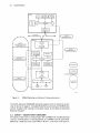
Figure 1-1
~)758
DPM50 Organization in a Typical DPM System
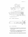
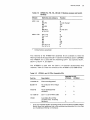
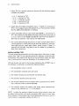
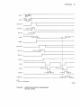
11.2 . 1 Distributed Plant Management Overview
DPM is a concept that connects a PDP-11 host computer to remote subsystems or terminals scattered through an industrial environment. DECdataway is the communication channel that links the host computer to
these remote subsystems.
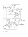
Figure 1-1 is a block diagram showing the DPM50 functional organization
in a typical DPM system. It shows a host computer linked to various rernote subsystems, including a DPM50, via a DECdataway. Refer to Figure
-1-1 throughout the rest of this discussion.
The DECdataway consists of an ISB 11-A interfaced to a PDP-11, and a
cable. The dataway cable is a twisted shielded pair cable up to 15,000
INTRODUCTION
3
feet (4572 meters) I'ong that integrates processes throughout a large industrial complex. Connectors are placed along the cable, creating ports
through which messages can pass to or from connected subsystems.
Communication over the DECdataway is synchronous serial at 55,556 bits
per second. The host computer maintains control of all communications
over the dataway. All transactions on the dataway consist of two messages: first, a command from the host to a port and second, a response
from a port to the host. There is one exception, the host can broadcast a
message to all ports simultaneously with no response allowed from any
port. Each port connector has address jumpers installed so the host can
select which remote to communicate with. A port can have more than one
address associated with it. This is the case with a port connected to a
DPM50 (which has two addresses). However, the number of addresses
per DECdataway cannot exceed 63. Therefore one DECdataway can accommodate 31 DPM50s at most. A more in-depth discussion of the DECdataway is presented in the DECdafaway User's Guide.
The DPM50 I/O subsystem is designed to monitor and / or control exte~nal
processes. It does this through the use of a variety of digital and anailog
input / output (I/O) modules.
The LSI-11 directly controls the I/O subsystem (and therefore the external process) by executing user programs located in its own local memdlry.
These programs are initially transferred by the host to the DPM50 aa a
series of messages over the DECdataway. These messages are received
by the ISV 11-A DECdataway interface and stored in the LSI-11 memory.
This transfer of information from the host to a remote is referred to as
downline loading.
The ISV 11-A also can accept data from the LSI-11 microcomputer. Upon
request from the host, the ISV 11-A formats and transmits this data upJine
to the host.
After down line loading a program into a remote DPM50 the host only has
to communicate with that task rather than control the external process
itself. If the DPM50 is gathering data, the LSI-11 microcomputer can preprocess the raw data before it is upline loaded to the host. This division of
work among various intelligent components in the system frees the host
to communicate with other remotes on the DECdataway. Therefore the
host maintains fundamental control over the entire system, but does so
efficiently by delegating most of the work to individual remotes along the
DECdataway. This arrangement typifies a DIGITAL Distributed Plant Management system.
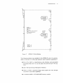
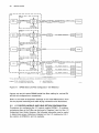
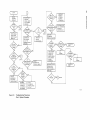
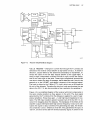
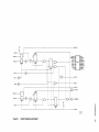
1.2.2 The DPMSO
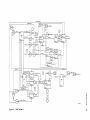
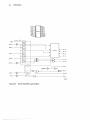
A detailed functional diagram of the DPM50 is given in Figure 1-2. It
shows the functional organization of major components and bus structures that make up the DPM50. The DPM50 is divided into the following
three main functional areas.
4
INTRODUCTION
r -,
I <! I
[
HOST
DECdataway
I~I~--------------.~
1;:0 I
ICfl I
L---1
-- ---
r;~;;-
I ~:;~;AY
L_____ ~:RFA:
I
I
I
I
TO
~
______
LSI-ll (KDll-H) OR
LSI-ll/23
(KDFll-AA)
LSlll
MEMORY
PROCESSOR
I
~~
II r-::E;
_ _ _ _I_SV_l_l_A
J
I
I
LSI-ll
MICROCOMPUTER
...
rl------=---=....:=-=-.:..~--.:....:.
~
~
~I--
...
LSI-ll BUS
LSlll BUS
I
L------- ______ I
I
I ~~;7~,
II
OPTIONAL
INTERFACE
BUS TO
TO OPTIONAL
~~~~~SDER
I
I
D-BUS
II'ITERFACE
~PT07
~
~
___ ~"-~"-D-"'::E.!'__ 1(0,
-
I
I'
1/0 SUBSYSTEM
J
L ____ _ ~[__________ ~~\LEDR~~R~NG
TO
PROCESS (ES)
•
MA 5506A
Figure 1-2
DPM50 Detailed Functional Diagram
The I/O Subsystem - interfaces directly to an external process
through a variety of digital and analog I/O modules.
The LSI-11 Microcomputer - exercises direct local control over the
I/O subsystem by executing user programs stored in its memory.
These programs are initially down line loaded from the host computer.
The ISV11-A DECdataway Interface - manages DPM50 communication with the host computer over the DECdataway.
INTRODUCTION
5
The next three sections describe each of the three main functional areas
in detail. Refer to Figure 1-2 throughout the discussion.
1.2.2. 1 I/O Subsystem - The I/O subsystem is capable o.f monitoting
and controlling a wide range of industrial processes. Applications range
from simple monitoring functions to controlling complex closed-loop systems. This flexibility is provided by the wide range of digital and analog 1/
o modules available. I/O modules are available to perform the following
functions.
Input Sensing
DC voltages
AC voltages
Change of state
Contact closure
A / D conversions
Event counting
Frequency measurement
Outputs Provided
DC switching
AC switching
One-shot dc switching
D / A conversions
Pulse trains
All I/O modules in the DPM50 share a common bus; the D-bus (Figure 12). The D-bus, in the DPM50 master chassis, can accommodate up to seven I/O modules. It can be extended through the optional H334 expander
chassis to add up to 70 I/O modules. This makes the DPM50 capable of
being configured with up to 77 I/O modules. Connections between U 0
modules and field wiring of external processes are generally made' at
screw terminal strips mounted on an H332 chassis.
The LSI-11 microcomputer (Figure 1-2) provides control over the D-I:)us
through the M7958 I/O Control Module (IOCM). This module interfaces
the LSI-11 bus to the D-bus. The IOCM accepts command signals from the
LSI-11 microcomputer and generates D-bus signals for routing data; to
and from the I/O modules.
Refer to the 110 Subsystem User Guide for more detailed information
about the I/O subsystem, the IOCM, and the I/O modules.
1.2.2.2 LSI-11 or LSI-11 /23 Based Microcomputer - The LSI-11 microcomputer directly controls the I/O Subsystem as described in the previous paragraph. The DPM50 LSI-11 microcomputer is based upon either
an LSI-11 (KD 11-H) processor or an LSI-11 /23 (KDF 11-A) processor (Figure 1-2).
NOTE: To avoid confusion, the following conventions are followed in t'his
user guide.
•
The term LSI- 11 microcomputer refers to the entire microcomputer
system, regardless of its processor.
•
When a distinction is made between processors, the option designation (KDXXX-X) is always presented.
6
INTRODUCTION
Tlhe LSI-11 microcomputer exercises direct local control over the D-bus by
executing user programs stored in its local memory. Within the DPM50
master chassis, space is provided in the LSI-11 bus backplane for adding
optional interface modules (Figure 1-2). This allows local terminals and /
or floppy disk mass storage units to be added to the system.
Complete information regardin~J the LSI-11 Microcomputer family of products is presented in the Microcomputer Processor Handbook and the Microcomputer Interfaces Handbook.
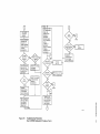
1.2.2.3 DECdataway Interface - The ISV 11-A is an intelligent DECdataway interface. It manages DPM50 communications with the host computer over the DECdataway. It performs the following functions.
1. It facilitates downline loading of the RSX-11 S operating system (with
built-in tasks) into the LSI .. 11 microcomputer memory. (Refer to Section 1.4).
2. It starts or halts the LSI-1 'I microcomputer in response to commands
from the host.
3. It allows bidirectional block transfers of information between the host
and LSI-11 memory.
4. Upon power-up or in response to a host command, the ISV 11-A runs
ROM resident diagnostic tests on itself and the LSI-11 CPU (processor and memory). (Refer to Chapter 3.)
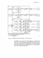
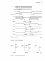
Figure 1-3 shows a detailed view of the ISV 11-A and its relationship to the
host computer and the rest of the DPM50. Through an IS8 II-A controller,
the host communicates over the dataway with the ISVII-A. The heart of
the ISV 11-A is an eight-bit microprocessor. This microprocessor executes
a microprogram resident in 5K bytes of onboard read-only memory (ROM).
It also uses 1K of random access memory (RAM) for stacks and local
storage (Figure 1-3). Communication with the host / DECdataway is handled by the microprocessor through a serial line unit based on an LSI synchronous communications chip. It is called a USYNRT (Universal Synchronous Receiver / Transmitter).
The controlling element in the process I/O portion of the equipment is the
LSI-11 microcomputer. Communication between the ISV 11-A internal bus
and the LSI-11 bus is through an interface in the ISV 11-A. The microprocessor and the LSI-11 can interrupt each other and swap specific information through shared I/O registers in the LSI-11 bus interface. However, the principal means of communication is the transfer of information
b(~tween LSI-11 memory and internal registers in the microprocessor. This
transfer is under microprocessor control via DMA logic in the interface.
Therefore, data from the host moves over the dataway, under microprocessor control through the serial line unit, internal microprocessor registers, LSI-11 bus interface, and eventually to LSI-11 memory. Once data
INTRODUCTION
DECdataway
HOST
ISB-11
-- -
-
-- -- -
I
I
I
I
-- - l
- -----1
~1-:-A---
I
I
7
SE RIAL LI NE
UNIT
I
I
(USYNRT)
8BIT
MICRO-
8 DATA LINES
16 ADDRESS LINES
BUS
1 I
PROCESSOR
LSI-11
LSI-11 BUS
L_
LSI-11
OR
LSI 11/23
PROCESSOR
LOCAL
MEMORY
BUS
INTERFACE
I
I
I
5K ROM
1K RAM
I
I
_ ______ J
LSI-11
MOS
MEMORY
16 DATA/ADDRESS LINES
LSl11
. .------~---------+----------~----~BUS
TERMINATOR
I
OPTIONAL
INTERFACE
OPTIONAL
INTERFACE
I
D-BUS
t
I/O
MODULE
UP TO 7
-------
I/O CONTROL
MODULE
I/O
MODULE
L_________
Figure 1-3
..J
The ISV 11-A in a DPM50 Subsystem
is there, the LSI-11 microcomputer can execute the data or operate on it.
Data from the remote makes its way back to the host via the reverse
route.
As stated earlier, there are 63 addresses available for ports on the dataway (address zero is not used). Each DPM50 uses a consecutive pair of
these addresses. The lower address is wired into the dataway port connector. From there it can be read by the ISV 11-A microprocessor. Since
an ISV 11-A uses two consecutive addresses, the highest address that
can be wired into a connector is decimal 62. Reading address 63 in the
8
INTRODUCTION
connector (octal 77, hex 3F) indicates to the 8-bit microprocessor that
the ISV 11-A is off-line (disconnl3cted from the DECdataway). Although the
dataway is half-duplex, using two addresses allows the ISV 11-A to appear as a full-duplex channel to tasks running on the host and remote processors. This is useful because there can be both a read request and a
write request outstanding at the same time. Which address is used for
which transaction is determined by higher level software.
A technical description of the ISV 11-A is presented in Chapter 4 of this
user guide.
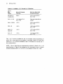
1.,3 PHYSICAL DESCRIPTION
The principle DPM50 standard components are as follows.
•
H333 master chassis with an H7870 power supply and an I/O control
module (LSI-11 bus to D-bus interface)
•
LSI-11 (KD 11-H) or LSI-11 /23 (KDF 11-AA) processor
•
MaS random-access memory (minimum 32K word)
•
ISV 11-A DECdataway Interface
1.3. '1 Standard Versions of the DPM50
Currently there are two standard versions of the DPM50. Each is offered
in a 115 Vac or 230 Vac input power configuration. Table 1-1 details the
variations.
Figures 1-4 and 1-5 show the physical arrangement of the components
within the H333 master chassis for the two standard versions.
For more detailed information about the H333 master chassis, the I/O
modules, and the IOCM refer to the 110 Subsystem User Guide.
1.3.2 Controls, Fuses, Indicators
The H333 master chassis front panel controls and indicators are on the
H7870 power supply (Figure 1-6). Table 1-2 details their functions.
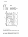
Figure 1-7 shows the five LED indicators on the M7958 IOCM. For more
information about these indicators, refer to Chapter 3 of the /10 Subsystem User Guide.
There are five LED indicators on the ISV 11-A module. Refer to Figure 3-2
and Section 3.5,1 of this manua.l for their location and function respectively.
INTRODUCTION
Table 1-1
9
DPM50-XX System Configuration
DPM50-XX
Standard Equipment
-AA, -CA
H333A master chassis
115 Vac
X
-AB, -CB -FA, -HA -FB, -HB
X
X
H333B master chassis
230 Vac
M7958 I/O control
module (lOCM)
X
X
KD 11-H LSI-11
microprocessor
(with KEV-11)
X
X
KDF 11-A LSI-11 /23
microprocessor
MSV11-DD 16 bit X 32 Kw
MOS memory
X
X
(Note 1)
(Note 1)
ISV 11-A DECdataway to
LSI-11 bus
Interface
X
X
TEV-11 LSI-11 bus
terminator
X
NOTE 1:
Modules
X
X
X
X
X
X
X
X
X
X
(Note 2)
(Note 2)
X
X
Originally shipped with two MSV11-GD 16 bit X
16K MOS Memory
NOTE 2: The ISV11-A must have EGO Rev 4 incorporated to operate in the
DPM50-Fx and -Hx versions.
1.3.3
Hardware Options
The following hardware options are available for all current versions of the
DPM50.
•
Cabinetry - The DPM50 is a cabinet or rack mountable device. Typical cabinets used for DPM50 mounting are DEC H960-C cabinets and
NEMA-12 cabinets.
•
I/O Modules - A wide variety of analog and digital input and output
modules is avaHable for the DPM50.
•
H334 Expander Chassis - This chassis is an extender chassis for
the D-bus and can accommodate up to 10 I/O modules. A single
DPM50 subsystem can accommodate up to seven (7) H334 expander chassis. This gives the DPM50 a total capacity for 77 I/O modules.
10
INTRODUCTION
CONNECTOR
BUS~
lE
M7958
10CM
1/0
I/O
~
LSI-11 BuS _________
1
---
l
[-n--ff- -n- -- ~'il ~~fl;1li
_J.
1-- - --~--ff--- -- -- - -- ----~- fl
MODULE
LSI1' T E R M I N A T O R _ r w -
~:PU;NSION
I
"OWOO"'"
r--
___
-H1- - -
----
III _ _
CONNECTOR
DBUS:::
~~~~ERS
14
--
_ _ _ __
13
12
-
- - --
_
11
10
8
7
DC ON ON
0
(!)
6
R
~LTC (!)
l
@
_l
l
I
_~
4~2
1--,--------ACON/OFF
5
RUN ENA
0
OFF
r;
L[ ij l[
__ _ _ _ _ _
9
+12V
H7870 POWER SUPPLY
-;-riJl
-----
I
+5V
(!)
I:l
r1-_FUSE
l:t"-1:::J-
HALT
I----AC IN
-POWER CONTROL
-----------M-A--S:"::T-ER-C--H-A:-:-SS--IS---------'--------'
(A) EARLY SHIPMENTS
CONNECTOR
<=;7
B
~~:~:"'~:~:;~:-=~~-~~--ff~n---n~
-1f----fI~ ~~--=-:~:pU;NSION ---J.D-- - t~ r- -- --- - - - - - - - - -III -::tJ-L
CONNECTOR -
D BUS ---- -
14
13
_ _ __
12
11
SLOT
--NUMBERS
-
_
10
+12V
H7870 POWER SUPPLY
_ _ _ _ _ __ _
9
(!)
8
-----===7=-----=6=----=5=---r=---=;:.--;::-;:,----:::-t
ON
DC ON ~
0
R
~LTC (!)
OFF
RUN
ENA
-
0 @
+5V
0
HALT
----------------------------------------~-----~
MASTER CHASSIS
(B) CURRENT SHIPMENTS
Figure 1-4
NOTE:
A G7272 CONTINUITY MODULE MUST BE INSTALLED IN ANY
UNUSED SLOT BETWEtN THE PROCESSOR AND THE ISV11 A.
DPM50-Ax, -ex Physical Layout
INTRODUCTION
11
CONNECTOR
LSI 11 BUS
<=;7
B
LSl11 BUs-__....
-- -r
I 1
"0 '000'-"
"---
~~~:ii'M'''we_-~~~=n~~~~--ff-~i}----n~
-n----fI~ ~~--~ -~:P~NSION _--+11-- - t~{- --- -- - -- --- ----III ---==-EJ=- ____ ._
__ _ _ _ _ _
CONNECTOR ___
D BUS
14
13
-12---11--10
~~~A~ERS
9
+12V
H7870 POWER SUPPLY
8
DC ON
0
(!)
7
R
@LTC
$
6
ON
0
RUN ENA
0 @
;5V
0
HALT
OFF
MASTER CHASSIS
NOTE:
A G7272 CONTINUITY MODULE MUST BE INSTALLED IN ANY
UNUSED SLOT BETWEEN THE PRoceSSOR AND THE ISV11A.
Figure 1-5
DPM50-Fx, -Hx Physical Layout
LINE
FUSE
®
+12 V
o
DCON
~
®
@LTC
OFF
RTN
AC ON/OFF
~o(~~t,
O®@ rn ~Jj
/L
\
RUN
HALT +5V
POWER
CONTROL
AC IN
MA·3!41
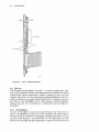
Figure 1-6
H7870 Power Supply
•
H332 Mounting Rack with Terminal Strips - This provides a convEmient point for connections between I I 0 modules and field wiring of
external processes .
•
H7006-A 18 Filter Panel - This provides EMI filtering for serial interface cabling (20 mA or EIA RS232C) connecting the LSI-11 to
modems or terminals outside the DPM50 cabinetry.
For information concerning the options listed previously (except the
H7006-A 18 Filter Panel), refer to the I/O Subsystem User Guide. Section
12
INTRODUCTION
Table 1·2
H7870 Switches and Indicators
Switches and
Indicators
Function
AC ON / OFF switch
Applies ac power to the H7870 and activates power
control outlet
Line fuse
Protects against ac line overload; fuse rating is 6.25
A for 115 V operation, or 3 A for 230 V operation
Power control outlet
When connected to power control bus, ties ac power
ON / OFF control of all power controllers to ac ON I
OFF switch of the H333 chassis
Ground lug
Provides safety ground connection to power supply
chassis
LTC switch
When on, enables B EVNT L which is an LSI-Bus
compatible line frequency signal generated by the
H7870 - must be on for normal operation
ENA I HALT switch
When on, enables program execution by the LSI-11;
when off it places the processor in halt mode - must
be in the ENA position for normal operation
DC ON indicator
Lights to indicate that dc power is on - should light
when ac ON IOFF switch is turned on
RUN light
Lights to indicate that LSI-11 processor is running
+ 5 V test point
Measures
+ 5 Vdc output
+ 12 V test point
Measures
+ 12 Vdc output
RTN test point
Meter return for dc voltage measurement
2.4.3 of this manual provides H7006-A/8 Filter Panel configuration and installation information. For information concerning the following options refHr to the Microcomputer Interlaces Handbook.
The following options are available for the DPM50-AA, AB, CA, and CB
versions. (Refer to Section 2.4 of this manual for option selection guidelines.)
•
DL V 11, DL V 11-F, or DL V 11-J Asynchronous Line Interface and associated terminals (becausB of cabling requirements the DL V 11-J can
be used only with the DL V 11-KA option)
•
DZV 11-8 Asynchronous Multiplexer Interface
•
RXV21 or RXV11 dual-drive floppy disk system (requires the REV 11
option for local boot capability)
INTRODUCTION
13
A1
81
C1
A
ION 1
E7
8
111111111
OFF
VECTOR
SELECT
V1
A1
8
STATUS
INDICATORS
CJ +5V
CJ
c::J
+12V
DEV SEL (DEVICE SELECT)
c:J
INTER (INTERRUPT)
c::J
TIMEOUT
V1
ADDRESS
SELECT
A1
,-A-...
E3.j""I'IIIIIIIU
t
C
OFF
INITIALIZE
SELECT
V1
A1
fOsCl--<>
D
~
V1
o
MA-0191
Figure 1-7
M7958 I/O Control Module
The following options are available for the DPM50-Fx and -Hx versions.
(Refer to Section 2.4 of this user guide for option selection guidelines.)
•
OL V 11-F or OL V 11-J Asynchronous Line Interface and associated
terminal(s) (the DL V 11-J can be used only with the DL V 11-KA option)
•
OZV 11-8 Asynchronous Multiplexer Interface
•
RXV21 or RXV 11 dual-drive floppy disk system (for local storage
only with no local boot capability)
•
An additional MSV 11-00 32KW MOS memory module
14
INTRODUCTION
1.4 SOFTWARE
The host software is based on the RSX-11 M or M-Plus real time operating
system. The LSI-11 microcomputer in each DPM50 subsystem uses the
RSX-11 S operating system. Both have software extensions to allow full
use of the Distributed Plant Management system.
Additional software at the hos't includes a device driver for the DECdataway and operating software to handle the following functions related to
the DPM50.
1. Downline System Load
The downline control task (DLC) is callable at the host through the
monitor console routine (MCR). It allows the user to download a system image to a DPM50 and initialize host-remote communication.
2. Upline Crash Dump
Another MCR-callable task, upline dump (ULD), allows the user to
bring the DPM50 system image to a disk file at the host. It is stored
there for later analysis by the RSX-11 M crash dump utility.
3. Interactive Program to Program Communication
An ancillary control procBssor (ACP) manages a single program-toprogram connection between the host and each remote. A host program written in MACRO-11 (010 interface) or FORTRAN IV + (CALL
interface) can communicate with a user program in a DPM50 using
ACP.
DPM50 diagnostic and maintenance software is discussed in Chapter 3.
Additional software for the LSI-11 microcomputer in the DPM50 includes
tlhe following.
•
ISV 11-A DECdataway driver
•
Complete support for the complement of process 110 modules
•
Language support for MP,CRO-11 and FORTRAN IV +
•
ACP to support the program-to-program link to the host
1.5 SPECIFICATIONS
Specifications for all LSI-11 microcomputer components in the DPM50 are
provided in the Microcomputer Processor Handbook and the Microcomputer Interfaces Handbook.
SpE!cifications for the remaining DPM50 components except the ISV 11-A
are provided in Section "1.4 of the //0 Subsystem User Guide. Specifications for the ISV 11-A are provided in Table 1-3.
INTRODUCTION
Table 1-3
15
ISV11-A Specifications
Features
Specifications
CSR addresses
160140, 160142, 160144
Interrupts
LSI-11 vector locations 300 and 304
Local memory in bytes
5K ROM (plus socket and address
decoding for another 1K), 1K RAM
Port addresses assigned
Two consecutive, lower wired into
connector on DECdataway
LEOs
M8080 - four programmable
54-13290 - modem dropout
Modem-dataway interface
Operating mode
Data format
Character size
Data rate
Transmission technique
Transmitter timing
Receiver timing
Line interface
Transmitted signal
Receivable signal
threshold
Error-free signal level
Common mode isolation
Receiver bandpass
Half duplex
Synchronous, serial, LSB first
8 bits (contains 0-2 stuffing bits)
55,556 bits-per-second
Biphase modulation
Crystal clock
Derived from received signal
Transformer coupled
5 V pop into terminated 200 ohm
cable
150 mV pop minimum
300 mV pop minimum
350 Vac rms, 500 Vdc
6 KHz to 130 KHz (-3 dB points)
The ISV 11-A places one dc and four ac loads on the LSI-11 and has the following
maximum current requirements.
+5V
+ 12 V
3.0 A
0.37 A
1.6 DOCUMENTATION
The following documents are shipped with the DPM50.
DPM50 User Guide
I/O Subsystem User Guide
KOF 11-AA User's Guide
Microcomputer Interfaces Handbook
EK-DPM50-UG
EK-OPIOS-UG
EK-KDF 11-UG
EB-17723-20
Microcomputer Processor Handbook
LSI-11 /23 Programming Card
LSI-11 Programming Card
MSV 11-0, -E User's Manual
ISV 11 Field Maintenance Print Set
EB-15836-18
EH-17898-20
EH-07043-53
EK-MSV 1D-OP
MP00609
16
INTRODUCTION
MSV 11-D Field Maintenance Print Set
H333 Field Maintenance Print Set
KDF 11-A Field Maintenance Print Set
KD 11-S Field Maintenance Print Set
TEV11 Field Maintenance Print Set
MP00566
MP00424
MP00734
MP00433
MP00074
The following related documents can be purchased from Digital Equipment Corporation. Information on where to order these documents follows
this list.
DPM50 Diagnostic User Guide
DECdataway User's Guide
Serial Bus Exerciser Writeup
Remote Terminal Tester Writeup
Diagnostic Monitor Wriiteup
CVPCADO Process Control Subsystem Writeup
EK-DPMOO-DM
EK-ISB 11-UG
MD-11-CZKCH-D
MD-11-CZKCI-D
MD-11-CZKMP-D
AC-A959D-MC
DPM I DPM-PLUS Documentation Set
Consists of four manuals:
QJ651-GZ
DPM I DPM-PLUS DECdataway Intelligent
Subsystem User Guide
DPM I DPM-PLUS Terminal User Guide
[)PM I DPM-PLUS System Generation
and Management Guide
[)PM I DPM-PLUS Release Notes
AA-J529A-TC
AA-J530A- TC
AA-J531A-TC
AA-J906A- TC
For additional references refer to Section 1.5 in the 110 Subsystem User
Guide, the RSX-11MIRSX-11S Documentation Directory (AA-2593E-TC)
and the RSX-11M-Plus Documentation Directory (AA-H426A-TC).
These documents can be ordered from the following address.
Digital Equipment Corporation
444 Whitney Street
Northboro, Mass. 01532
Attn: Communication Services (NR2 I M 15)
Customer Services Section
For information concerning Microfiche Libraries, contact the following
group.
Digital Equipment Corporation
Micropublishing Group
BU/D2
Bedford, Mass. 01730
CHAPTER 2
INSTALLATION
2.1 OVERVIEW
The DPM50 process I/O subsystem, with the addition of an ISV 11-A ()ECdataway interface, is similar to an IP300 process I/O subsystem. Therefore, most site preparation and installation information for the DPM50 IS in
the latest liD Subsystem User Guide (EK-OPIOS-UG). Chapter 3 of that
manual describes unpacking, inspection, installation, configuration, and
checkout procedures for a complete process I/O subsystem. However,
there are subtle differences between some versions of the DPM50 and the
IP300. Therefore, this chapter supplements the liD Subsystem tJser
Guide by providing configuration and installation information in the following areas.
H333
Cabinetry
ISV11-A
LSI-11 Bus
LSI-11 Bus Modules
D-Bus
Section
Section
Section
Section
Section
Section
2.2
2.2.2
2.3
2.4.1
2.4.2
2.5
The port connector on the DECdataway is of special interest to someone
installing the DPM50. The ISV 11-A cable plugs into this connector. The
connector is wired with the lower of the two port addresses that the
ISV 11-A responds to. For information on configuring the DECdataway port
connector refer to Chapter 3 of the DECdataway User's Guide (EK-ISB 11UG).
2.2 H333 INSTALLATION
The first part of this section gives general information applicable to alii installations. The remaining three parts give specific information about systems delivered in DIGITAL cabinets or mounted in NEMA enclosures or
other customer enclosures.
2.2. 1 General Considerations
Every cabinet used for mounting any equipment in a system must be properly grounded. The correct procedure is described in Section 1, Chapter 3
of the Digital Site Preparation Guide (EK-OCORP-SP).
17
18
INSTALLATION
Any enclosure or free·standing piece of equipment must be situated for
easy access and maintenance by Field Service. There must be good lighting and ample working space around the equipment. Wall-mounted enclosures must be a reasonable height above solid, safe, and roomy walkways. The site must also provide service outlets for scopes and other
maintenance equipment.
In the H333 there is a filter on the power line in the H7870 power supply. In
a standard DIGITAL installation, additional filtering is provided by an 861
series power controller. This controller has switched outlets that can be
used for other system units (tHrminal or disk) provided they are always
powered on and off with the 1-1333. Other equipment (scopes, maintenance gear, or system units that can be turned on or off independently of
the H333) should use independent outlets like the unswitched ones on
the 861. Better yet, such equipment should have its own separate filter.
The power checkout procedure in Section 3.4.1 of the I 10 Subsystem
User Guide indicates that supply voltages should be within three percent
of their nominal values. However, because of the ISV 11-A present in the
DPM50, the +5 V supply output must be adjusted to +5.1 V. To do this
follow instructions in Section 7.4.1 of the I 10 Subsystem User Guide.
Also, for normal operation the LTC and HALT / ENA switches on the front
panel of the supply must be up (ON and ENA, respectively).
2.,2.2 DIGITAL Cabinet Installation
W'hen a system is ordered in DIGITAL cabinets, all equipment is already
configured as shown in several illustrations in Chapter 3 of the liD Subsystem User Guide. The ISV 11-A cable is not shown in that manual. This
cable passes through the top of the H333 chassis and its dataway connHctor mounts on a bracket at the back of the cabinet (Figure 2-1).
2 . 2.3 NEMA Installation
Directions for installing the H333 and similar chassis in a NEMA enclosure
are given in Section 3,3.5 of the liD Subsystem User Guide. The bracket
holding the dataway connector on the end of the ISV 11-A cable must be
on an enclosure wall within 75 em (30 inches) of the right side of the H333
(Figure 2-1). Mounting requires a pair of holes for 10-32 hardware 0.554
cm diameter, drilled 4.445 cm apart (0.218 inches diameter, drilled 1.75
inches apart). Bracket location is unimportant as long as there is enough
clearance to connect the DECdataway port connector.
The H333 master chassis, each H334 expander chassis, and each H332
screw-terminal chassis has a ground strap on the right side. Everyone of
these ground straps must be electrically well-connected to the cabinet.
Although the RXO 1 and RX02 floppy disk systems are standard options
for the DPM50, DIGITAL does not supply hardware for mounting it in a
NEMA cabinet. Customers must provide their own mounting bracket.
2.2.4 NEMA Power Dissipation Considerations
A circulating fan with a minimurn capacity of 500 CFM must be mounted in
INSTALLATION
19
7015928-03
SERIAL BUS CABLE
BRACKET
H333-A. -B
MASTER CARD
CAGE
POWER SUPPLY
MA-2265
Figure 2-1
DECdataway Connector Mounting
the enclosure. An appropriate model is the Caravel 115 Vac, 550 CFM,
DEC PIN 12-04826.
A typical NEMA-12 enclosure with a fan (6 feet X 5 feet X 1 foot) can ibe
used to house an H333 and one H334. When there are two chassis in the
enclosure, the H333 should be at the bottom in the cooler circulating air.
Nothing else can be mounted in the box unless it is equipped with a heat
exchanger or air conditioner (both standard NEMA accessories). Even
then the remaining space should be used only for legitimate DPM50 <l>Ptions, expansion chassis for 110 modules, or screw-terminal chassis for
field wiring. No other equipment should be mounted in the box. Power dissipation of the enclosed units should never exceed 18 watts per squ~re
foot of uninsulated enclosure surface unless special equipment is installed to remove excess heat. The temperature of air circulating into the
LSI-11 area must never exceed 60 o C.
Heat produced in a NEMA cabinet can only dissipate through the walls of
the enclosure because the cabinets are totally enclosed, and lack external ventilation. The rate of heat loss through the cabinet walls is a direct
function of the temperature difference between inside the cabinet and ambient temperature outside the cabinet. Maximum operating temperature
20
INSTALLATION
for electronic equipment (LSI. memory, and other modules) inside the
cabinet is restricted to 60°C (140°F). Therefore, the maximum ambient
tBmperature in which a NEMA·-12 cabinet can be safely operated is also
limited by the following considerations.
1. Total heat (P) produced by all electronic equipment inside the cabinet
2. Total cabinet surface area available for heat dissipation
Therefore, a user considering factory floor installation for the DPM50 in a
NEMA-12 cabinet, must calculate the temperature limit within which the
system can be safely installed. For NEMA cabinets DIGITAL has tested,
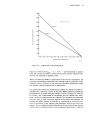
the following empirical relation holds true for the DPM50.
Pmax
=
2 X A (T 1 -
T 2)
Where:
P max
Heat produced by all the electronics equipment inside
the cabinet expressed in Btu / hr
A
Area of cabinet available for heat dissipation
T1
Maximum allowable temperature for the electronics for
any member of tht3 I/O subsystem family (T 1 = 60°C)
T2
Maximum ambient temperature where a NEMA-12 cabinet
is to be installed (OC)
For the cabinet under consideration (6 feet X 5 feet X 1 foot) the surface
area is 82 square feet. If the cabinet is mounted against a wall or otherwise obstructed on one 6 feet X 5 feet side, the surface area available for
heat dissipation is 52 square -feet.
For any given application, P max (the heat produced by the DPM50 subsystem) is calculated by adding the heat produced by the following things.
1. All I/O modules (See detailed module specifications in the II 0 Subsystem User Guide and use only the heat dissipation specified as
"due to field power source")
2. The power supply (See power supply specifications in liD Subsystem User Guide)
3. The circulating fan (180 Btu / hr)
For some devices, the heat specification is only available in watts (1 watt
== 3.41 Btu/hr).
INSTALLATION
21
10,000
9,000
Pmax
8,000
=
2 x A (T, T 2)
7,000
.L:
=>
~
Ol
Z
o
lJ.J
U
:::>
5,000
o
o
a::
a.
~
<!
4,000
lJ.J
I
X
E
a.
3,000
2,000
1,000
o~~--~--~--~--~--~--~--~----~--~--~--~
5
10
15
20
25
30
35
45
40
MAXIMUM SITE TEMPERATURE
50
55
00
°c
MA 6021
Figure 2-2
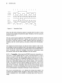
Cabinet Heat vs Site Temperature
Figure 2·2 shows the P max = 2 X A (T 1 - T 2) relationship in graphic
form. The curves are drawn to show the two most common cabinet installations, free-standing or against a wall.
When considering a NEMA-12 application for factory floor installation, ~he
total heat produced by equipment in the cabinet must be calculated. Then,
using the curve in Figure 2-2, the maximum allowable temperature where
the cabinet is being installed can be determined.
For applications where the temperature outside the cabinet exceeds allowable limits, additional cooling is required. NEMA cabinets available for
the DPM50 are provided with pipe fittings to allow circulation of clean air
for cooling. The compressed air introduced into the cabinet also maintains a positive pressure inside the cabinet. This protects the equipment
from dirt, dust, or other corrosive material in the factory environment. Air
purging the NEMA cabinet is achieved by connecting an air source to a
hole at the bottom of the cabinet, and opening a hole at the top of the
cabinet. The air supply should be filtered and oil free. It should also have a
shutoff valve to facilitate service, and a pressure relief valve in case the
22
INSTALLATION
cabinet exit port becomes obstructed. For a free-standing NEMA-12 installation, the following approximate relation between air flow, air temperature, heat dissipated, and ambient temperature holds true.
T:2 = T 1
+
1.8 A F (T 1 .- TA) - Pm a x
90
Where:
T2
Maximum ambient temperature where the NEMA-12 cabinet
is to be installed (OC)
T1
Maximum allowable temperature for the electronics for
any member of thE' I I 0 subsystem family, T 1 = 60°C
AF
Air flow in CFM
TA
Temperature of purge air (OC)
P max
Maximum heat produced inside the cabinet expressed in
Btu I hr
Therefore, a user considering NEMA-12 applications, must calculate what
temperature limits will allow rE~liable operations. These power dissipation
relationships were deriv~d under laboratory conditions and should only be
used as guides for most normal installations. For NEMA cabinet applications in areas with an abnormal heat source these formulas should be
modified to account for the specific environment.
The worst case dissipation for various chassis with all I I 0 slots filled is as
follows.
H333
H334 with power supply
H334 without power supply
2493 Btu I hr (713 W)
2319 Btu/hr (680 W)
955 Btu I hr (280 W)
To determine the exact figure for a particular configuration, refer to the I/O
Subsystem User Guide (the ISV 11-A dissipates about 17 watts).
2.2.5 Other Enclosures
Customers can use any enclosure they want to protect the equipment.
The mounting directions are the same as those given for a NEMA enclosure at the beginning of Section 2.2.3. However, when a non-DIGITAL,
non-NEMA cabinet is used, the customer must maintain specified environmental conditions, such as the quality of the system ground. In particular,
air circulating into the LSI-11 area must not be higher than 60°C.
2.3 ISV11-A CONFIGURATION
Physically the ISV 11-A is comprised of two quad-height modules bolted
together and connected by a e;O-conductor ribbon cable. Figure 2-3 shows
INSTALLATION
23
INTER BOARD
CONNECTOR
541329°1
OK
Cy~:OM
C]--PROM
8.42 in
213.87 mm
USYNRT
~HIP
CJ-~~OM
C]+-~~OM
C"Jr---4K
r-~
PROM
L---.J·~SPARE
@
_
SOCKET
@
(0)
SPACER
_ _ _ 10.44 in
___
-'
265.18mm
~
Figure 2-3
MA-2264
ISV 11-A Physical Configuration
the two boards joined together, along details of the ISV 11-A cable, dataway connector, and mounting bracket. As mounted in the chassis, the
M8080 mother board (the one that plugs into the backplane) is on the left.
This places the 54-13290 daughter board closer to the LSI-11 processor
board. The ISV 11-A must always be plugged into slot five of the backplane. (Refer to Figures 2-6 and 2-7 in Section 2.4.1).
All jumpers are set correctly at the factory. However, it is a good practice
to verify the configuration at installation time. An in-depth technical description of the ISV 11-A is presented in Chapter 4 of this manual.
Both ISV 11-A boards have a number of jumpers that are factory installed
for proper DPM50 operation. The jumper configuration on both boards is
as follows.
M8080
In: W7, W8, W9, W10, W17, W18, W19, W20
Out: All others
Jumpers
W1-8, W12, W13
W9-11, W14, W15
W16
W17,W20
W18, W19
W21-23
Use
LSI-11 bus address
Vector address
Hold on B SACK L
DMA timers
Connect pins
Reserved
24
INSTALLATION
Figure 2-4
64-13290
MaOaO Board
In: W 1, W3, W5, W7, W9
Out: All others
Jumpers
W7,W8
W1-W6, W9, V\l10
Use
PROM selection
PROM power
Figures 2-4 and 2-5 locate thf3 jumpers for M8080 and 54-13290 respectively.
:!.4 LSI-11 MICROCOMPUTER CONFIGURATION
The LSI-11 modules must be configured correctly for proper DPM50 operation. System configuration rE:lfers to the position of the LSI-11 modules
within the LSI-11 backplane, as well as switch and jumper settings on the
modules themselves. This section assumes a basic familiarity with the
LSI··11 bus. The reader who wants an in-depth discussion of the LSI-11
should refer to the Microcomputer Processor Handbook (EB-15836-18).
INSTALLATION
25
~
W1-W8
MA-2268A
Figure 2-5
54-13290 Board
2.4. 1 LSI-11 Bus Backplane Configuration
The recommended placement of LSI-11 modules in the LSI-11 backplar1le
is shown in Figures 2-6 and 2-7. Figure 2-6 shows placement of these
modules in the OPM50-AA, -AB, -CA, or -CB models. Some earlier versions
of these models were shipped with MSV 11-CO MOS memory modules.
The early version is shown in Figure 2-6A. The current version is shown in
Figure 2-6B. Standard equipment for these models include the following
features.
•
KO 11-H (M7264- V A, -VC) LSI-11 CPU with the KEV 11-A floating point
option
•
MSV 11-00 (M8044-0) 32K X 16-bit MOS memory
•
TEV 11 (M9400- VB) LSI-11 Bus Terminator
26
INSTALLATION
:2: -u
A) EARLY
SHIPMENTS
Q--
9
10
o
6
8
4
5
O~oO~O
MASTER CHASSIS (H333)
LSI-11 BUS
~ "RESERVED FOR I/O MODULES
'A G7272 CONTINUITY MODULE MUST BE INSTALLED IN ANY
UNUSED SLOT BETWEEN THE PROCESSOR AND THE ISVII-A.
B) CURRENT
SHIPMENTS
6
8
o
4
5
O~oO~O
MASTER CHASSIS (H333)
LSI-11 BUS
-----
~ "RESERVED FOR I/O MODULES
*A G7272 CONTINUITY MODULE MUST BE INSTALLED IN ANY
UNUSED SLOT BETWEEN THE PROCESSOR AND THE ISVII-A.
IFigure 2-6
DPM50-AA, -AB, -CA, -CB, LSI-11 Module Placement
8
o
~MSTE
LSI-11 BUS
6
5
4
O~oO~o
R CHASSIS (H333)
~ "RESERVED FOR I/O MODULES
'A G7272 CONTINUITY MODULE MUST BE INSTALLED IN ANY
UNUSED SLOT 3ETWEEN THE PROCESSOR AND THE ISVII·A.
Figure 2-7
MA-0231B
DPM50-FA, -FB, -HA, -HB LSI- '11 Module Placement
MA-0231 A
INSTALLATION
27
The DPM50-AA, -AB, -CA, and -CB supported options (one from each dategory) are as follows.
•
DL V 11, DL V 11-F, or DL V 11-J Asynchronous Line Interface (because
of cabling requirements the DL V 11-J can only be used with the
DL V 11-KA option) - Field Service requires this interface for terminal
connection to run local diagnostics.
•
RXV 11 or RXV21 Dual Drive Floppy Disk System - When this option
is selected the TEV 11 can be replaced with a REV 11 to provide local
boot capability.
The recommended placement of LSI-11 modules in the DPM50-FA, -FB,
-HA, and -HB models is shown in Figure 2-7. Standard equipment for these
models include the following features.
•
KDF 11-AA (M8186) LSI-11 /23 CPU - This can be upgraded with the
KEF 11-A floating point chip hardware option.
•
MSV 11-DD (M8044-D) 32K X 16-bit MOS Memory
•
TEV 11 (M9400-VB) LSI-11 Bus Terminator
The DPM50-FA, -FB,-HA, and-HB models support up to two (2) of the options listed below. However, Field Service requires an asynchronous line
unit to connect a terminal for diagnostic purposes. Therefore, if more than
one option is desired, one must be an asynchronous line unit. Customers
can choose from the following four supported options.
•
DL V 11-F or DL V 11-J Asynchronous Line Unit - Because of cabling
requirements the DL V 11-J can only be used with the DL V 11-KA option
•
DZV 11-B Four Channel Asynchronous Multiplexer Interface
•
MSV 11-DD 32K X 16-bit MOS Memory (additional)
•
RXV 11 or RXV21 Dual Drive Floppy Disk System - Because the LSI11/23 (KDF 11-A) and the REV 11 are incompatible, local boot of the
floppy disk system is not supported.
2.4.2 LSI-11 Module Configurations
All jumpers and switches on the LSI-11 modules are correctly set at the
factory. However, the configuration should be verified at installation time.
Location and function of the switches and jumpers on the modules can :be
found in handbooks supplied with the system. The Microcomputer Processor Handbook (EB-15836-18) supplies this information for the processor
and memory modules. The Microcomputer Interface Handbook (EB-1772318) supplies this information for all other LSI-11 bus options.
28
INSTALLATION
Table 2-1 shows the correct switch and jumper settings for standard modulHS shipped with the DPM50-AA, -AS, -CA, and -CB models. Table 2-2
contains the same information for the DPM50-FA, -FB, -CA, and -CB models.
Table 2-1
DPM50-AA, -AB, -CA, -CB LSI-11 Modules Jumper and Switch
Settings
Module
Switches and Jumpers
Position
KD11H
W1, W2, W3, W5, W6, W10 & W11
W4 & W9
W7 & W8
In
All Jumpers
SW 1, SW2. SW3, SW4 & SW5
SW6, SW7 & SW8
Remaining switches
In
On
Off
Does not matter
W16
All other jumpers
In
SW 1, SW2, SW4 & SW5
SW3, SW6, SW7, SW8
On
Off
MSV11 CD # 1
First 16K
MSV11 CD #2
Second 16K
Out
Do not change·
Out
OR
MSV11DD
W3&W2
PinW3
Pin 5-7
Pin 10-15
Pin 5-14
SWS5
In
On
·Critical factory parameter
Switch and jumper settings for additional LSI-11 option modules must be
SHt to integrate the option into the existing system. This must be determined at the time of installation. Directions can be found in the handbooks
referenced in the previous paragraph.
NOTE: If a DL Vll-J is incorporated into the system, its vector address
jumpers must be set 340 to avoid conflict with the ISVll-A.
2.4.3 Serial Line Interface Cable Filter (Optional)
The DPM50, mounted in a properly grounded H960 cabinet, is shielded
from the EMI / RFI radiation commonly found in industrial environments.
However, the EMI / RFI radiation may reach the cabinet via the interconnecting cable if the DPM50 LSI-11 microcomputer is interfaced to an
external terminal or other serial device. Attaching an H7006 filter option
where the cable enters the H960 eliminates this.
INSTALLATION
Table 2-2
DPM50-FA, -FB, -HA, -HB LSI-11 Modules Jumper and Switch
Settings
Module
Switches and Jumpers
KDF11-AA
W1
W2,W3
W4
W5,W6
W7
W8-W15
W16-W18
MSV11-DD
29
Pin
Pin
W2
W3
W4
W5
Pin
Pin
1 to 3
1 to 2
Position
In
Do not change·
Out
Out
In
Do not care
In
In
Out
In
In
Out
Out
10 to 14
16 To 15
In
In
Critical factory parameter
Two versions of the H7006 filter assembly kit are available to meet .the
filtering needs of all supported LSI-11 serial line interfaces used in a DPM50.
The H7006-A kit is used with the following LSI-11 bus options: DLV11,
DLV11-E, DLV11-F, and DZV11.
The H7006- 8 is used with the DLV11-J 4-channel asynchronous line
interface. Table 2-3 lists the contents of the H7006-A and 7006-8 kits.
Table 2-3
H7006-A and -8 Filter Assembly Kits
Quantity Per Kit
H7006-A
H7006-B
Part No.
Description
7423332-00
Filter mounting panel·
BC06K-7K
40 conductor mirror image
cable
o
H7004-B
40-pin bulkhead filter
assembly
o
7017399-06
DLV 11-J 20 rnA filter cable
o
4
H7005
8-pin Mate-N-Lok filter
assembly misc. mounting
hardware
o
4
Only one 7423332-00 filter mounting panel can be mounted per H960 cabinet.
Mount filters from additional kits in the existing mounting panel (no more than
six) if additional filtering is necessary.
30
INSTALLATION
r
rcAii'- - - - - - - .--...,
06:; -
-
-
---i
I
I
1
I
'TERMINAL CABLE
---------,
1H7006-A
I
,---
I
I
NULL MODEM *BC22A-XX
7423332-00
L ____ _ ~T:=:~E':J
~::l
MODEM
~--.:..:..:;==:.::.:---------------...,~::.J
f'H7006-A - -- - - - -
,_:]$1
_DZVll
BC06K-7K
[
1
;
M I F F M '----....r-....
I
L
L. ___ ~-
7423332-00
I
FILTER PANEL-I
t--:"'=":"':'=~=-==--I
I
NULL MODEM *BC22A-l0
I
=---=--=--_=-=}J
---8FEET--
---"---
NULL MODEM
*BC22A-l0
NULL MODEM
*BC22A-l0
SYMBOLS {
E/M = EIA RS232 25 PIN MALE CONN.
E/F = EIA RS232 25 PIN FEMALE CONN.
Figure 2-8
."
50 FEET
TERMINAL
E/M
(MAXIMUM)--------------~.,
M
F
= MALE CONNECTOR
= FEMALE CONNECTOR
DPM50 Serial Line Filter Configuration - EIA (RS232C)
Figures 2-8 and 2-9 show DPM50 serial line filter cabling for various EIA
and 20 rnA configurations, respectively.
Refer to the H333 arrangement drawings in the H333 Maintenance Print
Set for physical mounting and cable laying information and illustrations.
2.5
TERMINAL
*BC11U25
'TOTAL LENGTH BETWEEN MODULE AND TERMINAL OR MODEM,ETC. IS NOT TO EXCEED 50 FEET.
I/O CONTROL MODULE AND D-BUS OPTION CONFIGURATION
Procedures for configuring the I/O control module (IOCM), I/O modules,
and placing them in the D-Bus can be found in Chapters 3 and 4 of the I/O
Subsystem User Guide. However, the following information may be useful
in determining power limitations imposed on the I/O modules by LSI-11
bus options in DPM50··Fx and ·Hx systems.
TE Ri'IIll NAL
TERMINAL
INSTALLATION
31
TERMINAL CABLE
~--------,
IH700B-A
I
I
I
IL ____ _~~~E~J
7423332-00
IDLvii.K'A - -
I
- -
1(4 MAX.)
I
TERMINAL CABLE
~_ _ _~T.E~_RMINAL
CABLE
TERMINAL CABLE
M
N
L L
L
--1.----...r-'1i'""'7r7017399-0'AB--...------l--;Ii:·":":BC015_XX
I
L
=-=---...:.-= -,::-=- ___- -= =-=-.:.-=-I
L ___
..J.
7423332-00
FILTER PANEL
I (OPTIONAL)
J
I
-.J
"BC015-XX IS A OPTIONAL 20mA EXTENSION CABLE. AVAILABLE IN THE FOLLOWING LENGTHS: 3,B,10,
15,25,50,100 FT. SUBSTITUTE XX WITH DESI RED LENGTH WHEN ORDERING.
SYMBOLS
{
MNL; MATE-N-LOCK 8 PIN CONNECTOR
M
; MALE CONNECTOR
F
; FEMALE CONNECTOR
Figure 2-9
DPM50 Serial Line Filter Configuration - 20 rnA Current Loop
The DPM50-Fx and -Hx have seven slots available for I/O modules in fhe
H333. Due to power limitations, a close examination of power requirements for the I/O modules must be made based on which LSI-11 bus options are being used. The I/O modules use only + 12 V from the H7870
power supply. The maximum current needed for each I/O module is specified in the I/O Subsystem User Guide.
32
INSTALLATION
Table 2-4
Available
LSI-11
Bus
Option
+ 12 V Current for 1/0 Modules
DL.V11-F Console
Interface
DLV11-J/DLV11-KA
Console Interface
No option or
console only
2.63A
2.79 A minus 0.30 AI
DLV11-KA
DLV11-J/ .. KA
1.9 A minus 0.3 AI
DLV11-KA
Only one supported per
system
F~XV 11,
1.87 A
2.02 A minus 0.30 AI
DLV11-KA
DZV11-8
1.49A
1.64 A minus 0.30 AI
DLV11-KA
MSV11-D
(second)
1.42 A
1.57 A minus 0.30 A I
DLV11-KA
DLV11-F
1.75 A
1.9 A minus 0.30 A I
DLV11-VA
RXV21
The + 12 V current available for the I/O modules varies depending on
which LSI-11 bus options are present in the H333. Table 2-4 shows the
amount of + 12 V current available to the I/O modules for various LSI-11
bus configurations.
NOTE: Due to Field Service requirements outlined in Section 2.4.1, all
specifications in Table 2-3 arf} based on the assumption that a console
terminal interface (DL V11-F or DL V11-J) is present in the LSI-11 bus.
CHAPTER 3
MAINTENANCE
3. 1
OVERVIEW
WARNING: Do not initiate any DPM50 diagnostic or maintenance sbftware before checking with local site personnel for any safety precautions
to be performed and/or any operating restrictions. The DPM50 is a :remote process controller. Its I/O modules may control very sophisticared
and perhaps dangerous industrial processes.
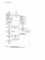
This chapter is divided into the following three main areas.
•
Sections 3.2 through 3.4 are devoted to DPM50 related maintena,",ce
software and firmware.
•
Sections 3.S and 3.6 contain information about the ISV 11-A and the
H7870 power supply, respectively. This is DPMSO specific information not found in the I/O Subsystem User Guide.
•
Section 3.7 contains DPMSO troubleshooting flowcharts.
Service personnel must take a system approach to maintaining a DPMso
with process I/O. This means distinguishing specific faults in the DPMSO
from system-wide faults, such as problems in the host computer or DECdataway. It also means taking into account the hierarchical nature of the
system. For example one cannot troubleshoot an LSI-11 bus device from
the host if the ISV 11-A connecting it to the dataway is not working properly.,-D.11 the other hand, once system integrity from host to LSI-11 is verified,
~st~nOard. LS1:11 bus diagnostics (MAINDECs) are run on the LSI-11 for
trQubleshooting devices and I/O modules. The host plays no role in such
troubleshooting except to download the diagnostics and communicate
with the operator.
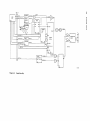
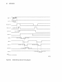
Figure 3-1 outlines the hierarchy of software and firmware used for
DPMSO maintenance. It shows the functional areas associated with each
software / firmware routine. Figure 3-1 can be used as an index to the particular paragraph in this chapter associated with each routine.
NOTE: Discussion of the above mentioned software/firmware routines in
this chapter is brief and of an overview nature. In-depth procedures for
running these routines can be found in the documentation listed in Section
1.6.
33
34
MAINTENANCE
HOST
CPU
11/70
OR
11/34
/ /
I
,,--- ..... ",
DZKCH
(PARAGRAPH 3.2)
\
I
\
I
CZKMPx
DIAGNOSTIC MONITOR
(PARAGRAPH 3.4)
L _________
I
,
I
.J
I
-1-I
I
I
CZKCI x
(PARAGRAPH 3.3)
I
MAINDEC'S
(PARAGRAPH 3.4.4)
I
I
I
I
J__
10CM
LSI-11 BUS
TO
D-BUS
INTERFACE
CVPCAx
(PARAGRAPH 3.4.5)
x=VERSION DESIGNATION
,,'---,
I
/
,
"
\
I
: DIAGNOSTIC:
: MONITOR I
I
I
\,
\
,
,
I
,
'......
\
.....
_--
Figure 3-1
\
/
I
" ..... __ .,. ""
I
I
,fill'
DPM50 Maintenance Software / Firmware Hierarchy
The North American (NORAM) industrial support team is chartered to provide all levels of support, including Field Service training for NORAM personnel. Support and training in European areas is provided by European
Regional Support.
3.2 DZKCH - DECDATAWAY EXERCISER
The ability of the host to communicate with a DPM50 via the DECdataway
must be verified before a valid diagnosis of a DPM50 can be performed.
DZKCH is a task that runs under RSX 11-M / M + in the host. This task ex-
MA 5!)06
MAINTENANCE
35
ercises the DECdataway and verifies integrity of the communicatidns
channel between the host and various devices on the dataway. Witn a
DPMSO, DZKCH checks communication up to and including the 8-bit Ihlicroprocessor in the ISV 11-A. It tests whether the 8-bit microprocessor
can manage the DECdataway protocol and communicate with the host.
3.3 CZKClx· AND ISV11-A ROM RESIDENT DIAGNOSTICS
CZKClx is also a task that runs under RSX 11-M / M + in the host. When
run, it starts internal diagnostics on selected devices connected to dataway ports. It receives and displays information on all but catastrophic errors.
With the DPMSO, CZKClx starts a series of ROM resident diagnostics in
the ISV 11-A. These tests also start automatically when the DPMSO is
powered up and can be used as a basic standalone confidence check for
the DPMSO.
As stated earlier, CZKClx can start the ISV 11-A microprocessor running a
series of diagnostic tests contained in its own ROM. As each test is executed, its test number is displayed in a set of LEOs mounted on the edge
of the M8080 board. Refer to Section 3.S.1 to locate and interpret these
LEOs. The first 9 tests (1-11 octal) are regarded as hardcore because
they test basic characteristics confined to the ISV 11-A. An error in any! of
these 9 tests causes the 8-bit microprocessor to loop within the test, thus
continuously displaying the number of the first failed test. Diagnostics 1214 (octal) check softcore characteristics involving the LSI-11 CPU (ptocessor and memory). Test 13 takes about 11 seconds, but 12 and 14 a:re
so fast their numbers may not be noticed in the LEOs. Errors in these tests
are not allowed to shut down the system. However, if an error occurs, the
test number flashes in the LEDs for 10 seconds and the number is up line
loaded to the host for display.
3.3. 1 Hardcore Diagnostics
The first 9 (1-11 octal) ISV 11-A ROM-resident diagnostic tests are considered hardcore. If a hardcore error is encountered, CZKClx fails and no error information is upline loaded to the host.
Table 3-1 describes the hardcore tests.
3.3.2 Softcore Diagnostics
Tests 12, 13, and 14 of the ISV 11-A ROM resident diagnostic tests are
considered softcore. For example, this type of error does not hinder the
ISV 11-A ability to communicate with the host. If a softcore error is encountered while running under CZKClx, error information is upline loaded to the
host and displayed at the operator's terminal.
Table 3-2 describes the softcore tests.
• x designates current version
36
MAINTENANCE
Table 3-1
Test
Hardcore Tests
Module
Description
M8080
Checks power-up configuration of 8080 I/O registers 1 and
2, and does basic 8080 instruction test
2
54-13290 Does individual cyclic redundancy check on each 8080 ROM
3
54-13290 Checks writing and reading in the 8080 RAM and checks out
RAM addresses
4
54-13290 Checks transmission and reception in USYNRT
communications chip using maintenance mode
5
54-13290 If dataway connector is unplugged (i.e., address 77 is read),
this test checks transmission and reception in the USYNRT
through the modem; otherwise test is skipped
6
54-13290 Checks ISV 11-A interrupt system
7
M8080
Checks 8080 I/O register 2 and 8080 I/O registers (3-5) that
are common with LSI-11 control and status registers (CSR2
and 4)
10
M8080
Checks timeout feature of DMA logic for access to LSI-11
memory
11
Both
Checks LSI-11 interrupt circuit in ISV 11-A
Table 3-2
Softcore Tests
Test
Module
Description
12
LSI-11
Loads a program into LSI-11 memory and then boots the LSI11 .- this checks ability of ISV 11-A to interrupt the LSI-11 and
vice versa
13
MSV11
Runs address and data tests on 28K words of LSI-11
memory
14
LSI-l1
Runs LSI-11 instruction test by loading it into LSI-11 memory
and booting the LSI-11 to run it
3.4 CZKMPx· DIAGNOSTIC MONITOR
If the ISV 11-A and its communications channel to the host are in working
order (i.e., DZKCHx and CZKClx have run correctly), service personnel
can execute standalone LSI-11 and I/O subsystem diagnostics in the
DPM50. This is done with a diagnostic monitor that runs in the host computer. This monitor comes with every DPM system host. It is accompanied
.)( designates current version
MAINTENANCE
37
by a set of LSI-11 bus diagnostics, in image format, kept on file at the
host. Note that the file names for these are the same as under XXDP but
with the extension .IMG. (For information on these diagnostics, refer to
Sections 3.4.4 and 3.4.5 of this user guide.)
CZKMPx allows service personnel to call various diagnostics for equipment on the LSI-11 bus in a DPM50 system. These diagnostics are downline loaded into LSI-11 memory and executed by the LSI-11. Host mode,
local mode, and communications mode are available for carrying out this
procedure. In host mode the operator remains at a host terminal and receives pass / fail and pass count information via upline reporting. Local
mode allows operators to go to the remote site and run diagnostics from a
terminal on the LSI-11 bus (connecting a portable terminal if necessary).
This method allows operators to call and run diagnostics from the local
terminal and receive complete error information. Communication mode is
similar to host mode with one major advantage. The operator stays at the
host terminal and receives not only pass/fail and pass count information,
but also error messages generated by the diagnostic running in 1he
DPM50.
CZKMPx runs as a task under RSX-11 M / M +. To run it, the operator tnters RUN CZKMPx in response to the MCR prompt character (». In response to further prompts, the operator selects the mode, gives the number of the DECdataway IS8 11-A controller, and gives the port address; of
the DPM50 to be tested.
3.4. 1 Host Mode
Host mode is used to verify, from the host, individual component op~r
ation in several DPM50s. It is not as comprehensive as the testing process conducted in local mode at the DPM50 site. However, it provides ian
efficient method for service personnel to verify basic functionality of remote subsystems scattered over a large area along the dataway.
After the port is selected, the monitor starts the ROM-resident diagnostics in the ISV 11-A. This takes the subsystem off-line. Failure of the port to
come back on-line is interpreted by the host as a hardcore error. In this
case a Field Service Technician must go to the remote site and fix the
ISV 11-A before that port can be further diagnosed from the host. Fot a
softcore error, the host reports which of the three softcore tests failed; In
any event, if the ISV 11-A comes back on-line, the operator can continue
selecting diagnostics to be run.
In host mode, the operator can select operation in single, script, or autoscript mode.
3.4.1.1
Single Diagnostic Mode - In single diagnostic mode the operator specifies a singlle diagnostic test to be called in from the disk. This
test can be executed directly, or the operator can elect to patch it. If
patched, the patched version can be saved, executed, or both.
~l8
MAINTENANCE
3.4. 1.2 Script Mode - In script mode the operator enters a series of
diagnostic file names. The task then saves the created script in a special
area on the disk, as well as executing the complete set. When this mode
is selected, CZKMPx displays the message "Enter diagnostics to be
scripted." The operator responds by listing diagnostic filenames and the
number of times each is to be executed consecutively. Items in the list
(filenames and numbers of passes) are separated by commas or a line
feed at the end of a line. The entire list is terminated by a carriage return.
The program then asks, "Do you wish to save this script?". A yes causes
the question, "Under what name do you want this script stored?". The
script is stored on the disk under the name given by the operator. However, a default name of ASCRPT is used if the operator responds to the
question with a carriage return.
The monitor then downline loads each diagnostic in the script and executes it. As each test is downline loaded, its name appears on the operator's terminal. When the scripted diagnostics have all been run, an end
message is issued and the operator is prompted to select a new mode.
3.4.1.3 Autoscript Mode - \"!hen this mode is selected, the monitor executes a script of diagnostics previously created in script mode.
3.4 . 2 Local Mode
In this mode, service personnel can communicate with the host for downline loading and running individual DPM50 diagnostics (kept on a disk at
the host). Since they are right there at the remote site, they can deal with
the equipment on the basis of information provided by the diagnostics.
Therefore, service personnel can alter their troubleshooting strategy dynamically and use the diagnostic in conjunction with other types of test
equipment (scopes, meters).
After selecting local mode, and the controller and terminal (dataway port)
numbers, service personnel must go to the remote site and connect (if
necessary) a portable terminal to the LSI-11 bus. At the local terminal,
service personnel can downline load diagnostics from the host and control their execution in the DPM50 using OOT commands.
3.4.3 Communications Mode
Communications mode is similar to host mode. However, communication
mode provides the operator with more detailed error information at terminals at the host. In host mode, the operator receives only pass/fail error
messages. If a diagnostic fails in communication mode, any error message normally generated by the diagnostic is up line loaded to the host
and displayed on the operator's terminal.
3.4.4 LSI-11 MAINDEC Diagnostics
The LSI-11 MAINDEC diagnostics in Table 3-3 are available for use with
the CZKMPx diagnostic monitor.
MAINTENANCE
Table 3-3
LSI-11 MAINDEC Diagnostics
DPMSO
Device
Diagnostic
Comments
CVKAACO
DVKABAO
CVKACC1
CVKADCO
CJKDACO
Basic Instruction test
EIS Instruction test
FIS Instruction test
Traps test
MEM Management
CJKDBCO
DVKAEB2
CPU - put a 1 in location 324
when running host mode
Floating point chip n / a
Floating point chip n / a
MaS / COR 0-124 Exerciser
tests only 28K in host mode
DLV11 test
CVDLABO
DL V 11-J test
CVDVCBO
Off-line test
CVDACO
Off-line test
DVDZAAO
DVDZBAO
DVDZCAO
DZRXAEO
DZRXBFO
ZRXDAO
CVPCADO
Four line ASYNC MUX test part 1
Four line ASYNC MUX test part 2
Cable and echo test
System reliability test
Interface DIAGS-NEEDS diskette
RX02 floppy
MDe I/O module test
KD 11-H
(M7246)
KDF11
(M8186)
KEF11AA
MSV11
(M8044)
DLV11
(M7940)
DLV 11-J
(M8043)
DLV11-F
(M8044)
DLV11-E
(M8017)
DZV11-B
(M7957)
RXV11
(M7946)
RXV21
IOCM
(M7958)
CJKDCBO
CJKDDBO
CZKMAFO
39
3.4.5 CVPCAx· I/O Subsy'stem Diagnostic
All information about the process I/O modules, the I/O control module on
the LSI-11 bus, and the H333 chassis power supply is provided in the 110
Subsystem User Guide.
CVPCAx is a complete diagnostic for testing the entire I/O subsystem.
The diagnostic and its use is described in the MAINDEC writeup (ACA959D-MC). Its use is discussed briefly in Section 7.5.3.2 of the 110 Subsystem User Guide. The new version is automated process testing (APT)
compatible and can, therefore, be run from the host. However, the only option that can be used when running from the host is the system test option, S. This option maps modules connected to the IOCM on the D-bus,
and runs the appropriate tests on them individually. Of course, the entire
diagnostic is used to its full capability if downline loaded from the host
and run in local mode from a terminal on the LSI-11 bus.
• x designates current version
40
MAINTENANCE
MSOSO
TEST POINTS
LEOS { -
TEST POINTS (
TP4
TP6
MA·2266
Figure 3-2
ISV 11-A Boards, Edge-on
3.5
ISV11-A
The maintenance philosophy for the ISV 11-A is option replacement. However, careful analysis of faults using diagnostics and available test points
should permit service personnel to isolate a problem to one of the two
modules. Section 3.5.3 of this user guide provides guidelines to aid in isolating a problem to one modulH. Note that the ISV 11-A operates only as a
unit, that is, with the MaOaO and 54-13290 boards connected together.
However they are not a matched set; a single board can be replaced if
necessary.
3.5. 1
LED Displays
As seen in the edge··on view of the boards (Figure 3-2), there are four
LEOs on the MBOaO board and one on the 54-13290. The single LED on
the latter board is lit whenever a message is being transmitted to or from
any port on the dataway - not just this ISV 11-A. The light goes out at the
€!nd of every message but goes right back on again as soon as the next
MAINTENANCE
41
message is detected. This is because the ISV 11-A receiver picks up· all
transmissions on the dataway including its own transmission to the host.
The light can be off for a significant time only if the dataway is inactive,
out of order, or if something is wrong with the receiver.
The LEOs on the M8080 board are all on at power-up. If they remain on,
the ISV 11-A is broken so badly that the onboard 8080 microprocessor
cannot even start its ROM resident diagnostics, which run automatically
following power-up. As the diagnostics run, each displays its number in
the LEOs (LSB at the top). The LEOs also signal failures (refer to Section
3.3).
Ouring normal operation, the 8080 rotates an off light from top to bottom
through the LEOs at a rate relative to the frequency at which it returns to
its background routines. This means that the LEOs cycle slowly when
there is a lot of dataway activity to the ISV 11-A. The cycling speeds upas
dataway activity decreases, and the LEOs cycle fastest when the syst~m
is inactive.
3.5.2 Test Points
The location and function of the ISV 11-A test points are presented in the
following discussion. This information is useful when troubleshooting the
ISV11-A.
Lugs for the test points appear near the LEOs in the edge-on board view
(Figure 3-2). On the M8080 the three test points are below the LEDs a;nd
are numbered 4-6 from the top down; on the 54-13290 they are above the
LEO and are numbered from the bottom up.
Maoao (Refer to Figure 3-3)
Point
Signal
Meaning
TP4
TP5
TP6
OMR H
FRPLY H
WAIT L
Internal OMA request
Failed to receive DMA reply
Force 8080 wait state
54-13290 (Refer to Figure 3-4)
Point
TP1
TP2
TP3
TP4
TP5
TP6
TP7
TP8
Signal
(including
print on which
it appears)
PCS2 BUS MEMR L
SL5 T OATA H
-+- 12 V through 1K
SL5 T ENA H
- 5 VB through 1K
-12 V through 1K
+5V
-5 VA through 1K
Meaning
8080 memory read
USYNRT serial output to modem
USYNRT transmit enable to modem
42
MAl NTENANCE
54-13290 (Cant)
Point
Signal
TP9
TP10
TP11
TP12
GND
SL 1 DROPOUT H
SL1RDATAH
SL 1 T CLOCK H
KHz)
SL 1 R CLOCK H
TP13
Meaning
No signal on dataway
Received data to USYNRT
Transmitter clock from !2 (55.556
Receiver clock to USYNRT
MA-2267A
Figure 3-3
M8080 Board
3.5.3 Module Troubleshooting
The following procedures are helpful if it becomes necessary to troubleshoot an ISV 11-A to one of its two boards.
Most ISV 11-A checks can be performed with the modules installed because all test points and LEDs are located at the module edge. However,
when it is necessary to access internal points on the boards, use the following set-up procedure.
MAINTENANCE
43
USYNRT
NEGATIVE
VOLTAGE
CONVERTERS
o
o
PROM 0
PROM 1
PROM 2
PROM 3
PROM 4
SPARE
PROM
SOCKET
MA-2268B
Figure 3-4
54-13290 Board
1. Remove the ISV 11-A module set.
2. Install two double height module extenders, or one quad extender.
3. Remove the six screws that join the MaOaO to the 54-13290.
4. Reverse the 54-13290, align its outside edge with the outside edge
of the MaOaO, and join them with three screws. Make sure the short
ribbon cable still connects them.
5. Plug the MaOaO into the module extender.
QUICK CHECK FOR MAJOR PROBLEMS
These tests check the major functionality of ISV 11-A modules. They are
particularly useful if the aD aD does not run (all maintenance LEDs on). Unless otherwise indicated, all test points are on the outside edge of the 5413290. Testing requires a voltmeter and an oscilloscope (preferred) or
logic probe.
NOTE:
TP7 (+5 V) and TP9 (GND) can be used to power the probe.
44
MAINTENANCE
1. Using TP9 as a ground reference, ensure that the following supply
voltages are present:
+ 5 V ± 5 percemt at TP'l
+ 12 V ± 5 percent at TP3
--12 V ± 10 percent at TP6
-5 VA ± 5 percent at TP8
- 5 VB ± 5 percent at TP5
2. Check that the modem transmitter clock, T CLOCK H, is present on
TP 12. It is a square waVf~ with period 18 /-ls. This test also verifies
that the 8080 clock generator is working.
3. Check that 8080 memory read pulses, BUS MEMR L, are present on
TP 1. This verifies that the 8080 is fetching instructions and running. If
it is not, verify on the MB080 that BPOK H (E 14-12) and READY H
(E70-23) are asserted. Then replace the 8080 (E70).
4. The carrier detected LED should turn on (dim or bright glow) when a
running dataway is connected and off when the dataway is removed.
If the LED stays on, check that T ENA L (TP4) is high. If T ENA L is
asserted, the USYNRT chip (E20 on the 54-13290) or the 8080 program flow is defE~ctive.
MANUAL MODEM TEST
This test should be performed if test 6 (modem test) in the power-up diagnostics fails. Test 6 is not executed unless the dataway is disconnected.
Furthermore, this manual test should not be performed unless the dataway is disconnected to prevent disruption of its ongoing activity.
The test checks out most of the circuitry interfacing the USYNRT chip to
the dataway. In particular, it verifies the following things.
1. The transmitter turns on and off.
2. The transmitter transmits ones and zeros.
3. The modem analog circuits transmit and receive data.
4. The receiver decodes ones and zeros.
5. The receiver detects the sync pattern (two successive zeros following a one) that locks in carrier detected.
6. The receiver detects thE~ pattern that drops carrier detected (absence of any transition for 1-1 1/2 bit times).
NOTE: In either the analog or digital circuitry of the receiver, there may
be subtle failures which can cause occasional GRG errors or other prob119ms. However, these failures may not be detected by this test or test 6. If
such a failure is suspected, fE~place the ISV11-A.
MAINTENANCE
45
The following tools are required to perform this test .
•
Two 6-inch jumpers with alligator clips or miniclips at each end
•
Oscilloscope (or logic probe)
Success or failure is determined by observing the state of the carrier detected LED after each step.
Effect
LED
1.
Power up ISV 11-A with dataway
Transmitter idle
Off
2.
Connect jumper 1 from TP4
(E ENA L) to TP9 (GND)
Transmit 1s
Off
3.
Connect jumper 2 from TP2
(T DATA H) to TP9 (GND)
Transmit Os
On
4.
Disconnect jumper 1
Transmit 1s
On
5.
Disconnect jumper 2
Transmitter idle
Off
If the test fails, repeat it, observing these points with the scope after each
step.
Step
1
2
3
4
5
R CLOCK H (TP13)
Logic 0
Logic 0
Square wave (18 j.ts)
Square wave (18 j.ts)
Logic 0
R DATA H (TP11)
Logic 1
Square wave (18 j.ts)
Logic 0
Square wave (18 j.ts)
Logic 1
3.6 H7870 POWER SUPPLY
In a DPM50, the ISV11-A is mounted in an H333 chassis which contains
its own power supply. The HALT lENA switch on this power supply mustbe
set to ENA. Furthermore, the + 5 V output of the supply must be in ~he
+ 5.1 V ± 0.15 V range. Instructions for adjusting the supply are given in
Section 7.4.1 of the liD Subsystem User Guide.
3.7
DPMSO TROUBLESHOOTING FLOWCHARTS
WARNING: Do not initiate any DPM50 diagnostic or maintenance software before checking with local site personnel for any safety precautions
to be performed and lor any operating restrictions. The DPM50 is a remote process controller. Its 110 modules may control very sophisticated
and perhaps dangerous industrial processes.
The rest of this chapter is a series of flowcharts (Figures 3-5 through 3-8)
that define a troubleshooting procedure for the DPM50.
I
I
INFO FROM
CONSOLE, ERROR
LOG, CUSTOMER
COMPLAINT
INVESTIGATE
POSSIBILITY
OF PERIODIC
ELECTRICAL
INTERFERENCE
s:
~
Z
--1
m
Z
I
»
z
RUN STAND-ALONE
ISB-11 DIAGNOSTICS
(")
m
SUSPECTED ISB-11
II
CHECK CONSOLE
OUTPUT & RUN
ISBRPT TO DUMP
ERROR LOG
CHART
WITH PHYSICAL
LAYOUT FOR
FAULTY DE\/iCE
POSSIBLE DATAWAY
21
II
GO BACK TO
START
INSPECT
DATAWAY FOR
PHYSICAL DAMAGE
SUPPORT
RUN DZKCH ON DEVICE
COMBINATIONS,
RUN APPLICABLE
DPM50 DIAGNOSTICS
FROM HOST
GO BACK
MAINTENANCE
WHEN DPM50
CAN BE RELEASED
DETERMINE
SPARE MODULE
AVAILABILITY
AND SCHEDULE
REPLACEM ENT
Figure 3-5
ARRANGE FOR
INTEGRITY OF
REMOTE PROCESS
WHILE DPM50 IS
RUNNING
DIAGNOSTICS
ADVISE
CUSTOMER OF
PROBABLE CAUSE
OF FAULT
Troubleshooting Flowcharts
Chart 1 System Procedure
AT DPM50
CHECK +5V. +12V.
LTC; POWER DOWN
DPM50; DISCONNECT FIELD
SIGNALS AS
NECESSARY;
REPLACE KNOWN
FAULTY MODULES;
INSTALL
TERMINAL IF
NECESSARY;
POWER UP DPM50 &
TERMINAL:
OBSERVE ISV-llA
HAVE CUSTOMER
ARRANGE FOR
INTEGRITY OF
REMOTE PROCESS
WHILE DPM50 IS
RUNNING
DIAGNOSTICS
CALL
SUPPORT
INTERPRET
ERROR REPORTS
TO DETERMINE
FAULTY MODULE(S)
REPLACE
ISV-llA
MONITOR; RUN
APPLICABLE DPM50
DIAGNOSTICS IN
HOST MODE
SUSPECT 1/0 DRIVERS
OR RECEIVERS NOT
TESTED BY
DIAGNOSTICS
INTERPRET
ERROR REPORTS
TO DETERMINE
FAULTY MODULE(S)
SET UP MONITOR
FOR LOCAL MODE:
TAKE SERVICE
EQUIPMENT TO
REMOTE SITE
CHART 3
TERMINAL IS ON
LINE TO MONITOR;
RUN APPROPRIATE
DIAGNOSTICS TO
VERIFY REPAIR
GO TO DPM50
s:
~
z
~
m
Z
»
z
(")
m
Figure 3-6
Troubleshooting Flowcharts
Chart 2 DPM50 Subsystem Procedure, Part A
4B
MAINTENANCE
EXIT MONITOR;
POWER DOWN
DPM50; REMOVE
EQUIPMENT THAT
IS NOT PART
OF SYSTEM;
RECONNECT FIELD
WIRING; POWER UP
DPM50; MAKE SURE
ISV-11 A ROM TESTS
PASS
CUSTOMER
HARDWARE
IS CAUSING MODULE
TO FAIL. OR THAT
SPARE MODULE IS
BAD
RELEASE SYSTEM
TO CUSTOMER FOR
APPLICATION
TEST
PERSISTS.
CALL SUPPORT
DONE - CLOSE
UP & DO
PAPERWORK
MA·2427
Figure 3-7
Troubleshooting Flowcharts
Chart 2 DPM50 Subsystem Procedure, Part B
MAINTENANCE
49
ADDRESS WITH
EXPECTED ADDRESS &
ADDRESS WIRED IN;
INSPECT CONNECTOR
& CABLE FOR SHORTS,
OPENS, LOOSE PINS
CHART 2
PART A
ISV-llA
CABLE
POWER UP
AGAIN WITH
DATAWAY
VERIFY OPERATION OF TERMINAL
VERIFY THAT MONITOR IS RUNNING AT HOST
CHART 2
PART A
Figure 3-8
CONSULT DATAWAY
USER'S GUIDE
AND TM
Troubleshooting Flowcharts
Chart 3 Port Address Checkout
CHAPTER 4
SYSTEM LOGIC
4. 1 OVERVIEW
The ISV 11-A is a dual quad-height printed circuit board option. It is built
around two large-scale monolithic integrated circuits, an BOBO microprocessor, and an LSI synchronous communications device (USYNRT). In
order to understand how the hardware functions, readers must be familiar
with the operation of these two circuits as explained in the vendor manuals. A signal name glossary has been provided at the end of this manual.
Figure 4-1 is a block diagram showing the logical organization of the hardware on the MBOBO ISV 11-A microprocessor and the 54-13290 serial line
unit. Logically the system has three major subdivisions organized around
two internal buses, one of which is simply an extension of the LSI-11 I:)us.
The processing unit is comprised of elements of both boards and is shcl>wn
in the upper left quarter of the figure. It includes the BOBO microproces$or,
its associated clock and gating circuits, and local memory. Communication between microprocessor and local memory is over the BOBO bus.
This bus runs throughout both boards, connecting the processing unit to
the other two major parts of the logic. The interface between the BOBO bus
and the DECdataway is shown in the upper right quarter of the drawing,
contained entirely on the 54-13290 board. This subsystem is based on !the
USYNRT communications chip and connects to the dataway by a mod~m.
The remaining hardware is shown in the lower half of the figure, contained
on the MBOBO board. It includes registers, decoders, and other minor Idgic
elements that connect the BOBO bus to the LSI-11 bus. The LSI-11 bus in
turn connects to the LSI-11, its memory, and peripheral equipment.
The hardware on each board is shown in a set of circuit schematics, code
CS. Each set has a drawing number in the form X-0-1 (X is the board designation). A revised schematic has a revision letter to the right of ithe
drawing number. For convenient referencing the individual sheets of each
drawing set are labeled. For example, the labels on the six sheets of 5413290-0-1 are SL 1-6, and those on the eight sheets of MBOBO-0-1 are
PCS 1-B. These labels are lIsed as prefixes in signal names to indicate
signal origin. They are also used in the text and the block diagrams for
referencing individual prints. In Figure 4-1 these labels appear in the lower
left corners of each block to indicate which print contains the logic represented by the block. Parts of a print are indicated by combining the lettrers
51
REs:rROCEssI.NGru-N-T------------,r-------------~+r-rl------~I---------rI.______S_E_RI_A_L_L_IN_E__
UN_I~TI
S224
CLOCK
PCS 2
:
INTI
H
PCS 2
L
j
ADDRESS
822S &
S241
DRIVERS -
PCS1 J1
SL6 J2
H
INTERRUPT
PRIORITY
I [",
+
SL3
MEM
BUS
~SL2
SL2 t
2X8/
....-------.
RAM
}_
1----.1
I
I
DECdataway
~V~
"'2 TIL
CONNECTOR
L
USYNRT
~SL5
f - -----,
CONTROL &
STR08E
j~~' I::~~;:
0"1
N
I
I
Cf)
-<
Cf)
-l
SL1.4
ROM
SL3 5KX81
S080
I
I
iA3-7
tI I !
i
<il2 TTL
I
~C~O~NTI:-::R~O~L"'_
PORTS
r-
80-87
I I
~U
""'---.---'
r r
m
:5:
I'
All
MODEM
ISL 1
~ ~
4
INTE:RUPT PORT AO -
I
I~----I
r
0
C>
C"')
DATAWAY
PORTS
STATUS
SA-SF
PORT 90
"',
~g~~~~s
(I
t
•
•
•
~
I
I 'US IADD",ss ~:~-~ -- --I-::'~ ---- -~~:::~7 I CD- ~ ~D: - - - - - - -- -- -- - - -- - - - - - - ----- -- - ------ - --~--I.f----~--r--+-.--+-.~--''-+-I--+-~--'rl~~:TROL I J-r- ~~~ERRUPT 1---_+-_____--+-___--,
-0PSCOS 2 _
'
SL2 1 KXS
DATA t
BUS DO-7
SL5
SL5
7XS
SL5
5XS
SL5
S
SL4
6
S -
8
PORT 2
pcs 7
S
L_
DMA DRIVERS
PCSS,
IDMA DRIVERS
16
pcLSS
~6
~
IDMA DRIVERS
pcLSS
P~5rT·6 I-,---i
ii'
CONTROL
~I
l
;6
PCS4
PORT 1
~--IHf---f----tlpcs 7
~~--~
S
I -.J
j 1
I
PORTS 1 &2 \
2XS\
I
I
tt,tl~
S641
~ ~~~~:~~IVERS ......+-+-..;.CO.;.N..;.T..;.R;.;O;.;L....;;L..;.IN.;.;E;.;;S-+________+r"-____+-__...L____+ ____-+.....J______..z..
+ __-+________--iJ
7
S0
PCS S70
ADDRESS
PCS 4MATCH
::
4
n
+
.-D
rpc:SsRO
J
4J
3
OpO- RT 5 .\
DE~~~~RS Uf----'------+--------L-------'----+-.,.4---CS+R-o---+tILP~~~ 44
PORT 4
PCS 3
I
PORT 3
CSR 2
r-----t-j------t-----t-~P~C~S~4~--J
rn;~~I----..,._+_+_------t_-----l----tt_-------2V!E~CT~O:!..!:R~~
~
LSI-ll INTERFACE
DAL 0-3
PCS 7
Dm~
DM~2
BUS
DAL 0-15
INTERNAL LSI-ll BUS EXTENSION
DAL
DAL 0-3
TRANSCEIVERS ......~~----------~--------~------~----------------------~----------LS-I-I!-O-A-D-D-R-E-S-SE-S--l~60-1-4-0-+--CS-R~N-UM--B-ER--~------~------~
7
PCS 4
B DAL
°
Figure 4-1
16
ISV 11-A Logical Organization
SOSO MEMORY ADDRESSES FOR PORTS: 4000 + PORT NUMBER
j \
16
SYSTEM LOGIC
53
and numbers along the edges. The following three sections give a detailed description of the hardware on the two boards. Discussion is
geared to the prints, but readers should also refer to Figure 4-1 whenever
necessary.
Some logic signals on the boards are available at test sockets shown in
the lower-left on SL6 and the upper-right on PCS6. In some cases the
lines to these test pins are not true logic signals at all, but gate inputs tied
to +5 V. Therefore, they play no real role in system operation, but they
can be pulled low to disable various parts of the logic for GR test purposes. These pseudosignals are identified on the prints by the word test.
4.2 PROCESSING UNIT
This unit occupies part of both boards and is shown on three prints; PCS2,
SL2 and SL3. The first of these shows the 8080 microprocessor with i~s
clock and gating circuits. The 8228 has bidirectional drivers for the 8 data
lines in the 8080 bus; the two 7 4S241 s below it provide unidirectional driving for the 16 address lines. The 8224 clock circuit at the left supplies the
¢ 1 and ¢2 clocks for the microprocessor chip, and the ¢2 TTL clock for Une
serial line unit (all clocks are 2 MHz). At the beginning of every micrbprocessor machine cycle the 8080 places status information identifying
the use of the cycle on its 0 outputs, and sends a sync signal to the 8224.
This latter chip responds by sending a strobe to the 8228, causing it to
load status into a set of latches. This frees the data lines for transfers
during the cycle. The status information indicates the kinds of events that
occur during the cycle. From the latched status bits and 8080 control signals WR and DBIN (write and data bus in), 8228 sets up memory, I/O cohtrol signals, and interrupt acknowledgement for the cycle. A memory read
is for fetching an instruction, an operand, or an item from the stack; writing in memory can be for an operand or a stack item. Bus I/O control signals (in field 01 on the print) are produced by the 8228 I/O outputs. However, they are also asserted by the memory control signals when the
address is in the 4000-7FFF range. That is in the area of the ISV 11-A address space reserved for I/O registers.
The ready input to the 8080 through the 8224 should always be high, except when a wait is required for a DMA operation. ENA DMA enables tne
8093 so that WAIT goes low; when the acknowledgement appears,
READY goes high and the 8080 continues. But, the DMA signals have rio
effect when I/O WR is true. This is done to prevent an unwanted wait from
hanging up the 8080 if DMA signals are generated inadvertently because
an I/O operation looks like a DMA operation to DMA logic. When the 8080
do·es an input or output instruction, it puts the one-byte address on both
the upper and lower half of the address lines. Therefore an I/O port address of 80 or above puts a 1 on line 15, which may generate ENA DMA.
The I/O WR prevents any wait during an IN instruction, but during an OUT
it occurs later and the 8080 may enter the wait state for a single cycle.
The RAM and ROM that constitute local memory are on SL2 and SL3 respectively. The RAM is made up of 8 1K X 1 chips, each storing a single
54
SYSTEM LOGIC
bit of each byte in the 1K. Whereas the ROM is made up of 5 1K X 8 chips
(with space for a sixth), each storing the entire byte for 1K locations. Logic gates at the upper-left on SL2 produce a memory select when the 8080
calls for a memory read or writc3 with an address in the 0-1 FFF range. The
select, in turn, enables the decoding of address bit 10-12 at the lower-left
on SL3 to select a single ROM chip or the set of eight RAM chips. The 10
least significant address bits are applied to the address inputs of all chips
to select the individual location. When the RAM is selected and the function is write, bits from the eight data lines are written into the eight RAM
chips. The output of the selectl3d ROM, or set of RAMs, is available on the
SL3 memory bus. During a read, the data is placed on the 8080 bus via
the multiplexer at the upper-ri!Jht on SL2. Drawing TD-ISV 11 A-0-7 shows
the timing of the signals involvHd in the 8080 reading and writing memory.
4.3 SERIAL LINE UNIT
The heart of this unit is the USYNRT synchronous communications chip at
the left on SL5. It is set up for byte operation by a high level at pin 22 and
connecting corresponding pins for the left and right bytes of its 16 data
inputs-outputs. These connect to the eight data lines of the 8080 bus. The
8080 governs the device by supplying control bytes and reading status.
The USYNRT in turn uses the modem for handling communication over the
serial DECdataway. Serial data received from the modem at RSI is assembled into bytes, and is available to the processing unit via the eight data
lines. Transmit bytes supplied over data lines are passed on serially to
the modem from TSO.
The 8080 moves bytes to and from the interface by means of its I/O ports.
Port selection is made by the address decoder at the right on SL4. The
number of ports is small, and an I/O bus control signal is generated by
either an I/O transfHr or memory access in the appropriate address
range. Therefore, decoding a few address bits and the I/O signals is sufficient to select among ports 90, AO, 80, and the USYNRT registers. From
port 80 the 8080 can learn its own dataway port address, wired into the
DECdataway connector and available through the gates at the left. SEL
8X enables the USYNRT data lines. Selection among various registers is
made by address bits 0-2, applied to the USYNRT address inputs on SL5.
Register reading and writing uses separate addresses, so A03 is connected to the USYNRT write input. A one enables writing and drives the
USYNRT data lines from the 13080 bus through the two 7 4S241 s at the
lower-right. When a zero places a register on the data lines, READ 8X
from the address decoder drives the 8080 bus from them. The E30 gate
below the decoder on SL4 pn3vents register selection at all if the 8080
should give a read function for a write port.
The remaining 2 ports are at the upper-right on SL5, where address 90
reads status bits from the USYNRT and the modem, the LSI-11 interrupt
request through E22. Address AO loads a byte from the 8080 bus into the
register in E27. The control bits supplied include enables for transmitter
and receiver in the USYNRT maintenance mode, and for various conditiions that can request interrupts through gates at the upper-right. Selecting maintenance mode inhibits generation of the transmit enable to the
SYSTEM LOGIC
55
modem (T ENA at CI), even if the USYNRT transmitter is active (TX ACT).
The interrupt request levels are applied to the latch and priority network
at the upper-left on SL2. Any interrupt request produces the INT signal,
which goes to the a080. Response by the aoao with an acknowledgement
latches the current request, enables the multiplexer for the SL2 bus (a080
bus data lines), and selects as multiplexer input an RST instruction encoded from the number of the highest priority request. The 8080 then executes the RST as a call to the corresponding location (as listed in the
table at the lower-right on SL5).
4.3. 1 Serial Transmitter-Receiver
The modem for the serial line unit takes up most of SL 1. The basic time
reference is the ¢2 TTL clock supplied by the a224 clock circuit associated with the aoao microprocessor. This clock drives the receiver
directly. For the transmitter, the exclusive OR gate at A7 (with the delay
introduced by two inverters at one of its inputs) acts as an edge deteator
to multiply the basic clock to 4 MHz. From this, the E2a counter produces
the ax clock by dividing by nine. This is accomplished by loading 7 at the
clock following the carry out produced by a count of 15. The ax clock
counts the E23 counter, which runs on a continuous 16-count cycle sol its
two middle bits provide division by 4 and a. The T (IX) clock drives the
USYNRT transmitter and shifts out the data; the 1X and 2X clocks together are used for biphase encoding of data transmitted over the dataway.
Characteristics of the various clocks are as shown in Table 4-1.
Table 4-1
Clock Characteristics
Clock
Period (IlS)
Frequency
¢2TTl
0.5
2 MHz
8X ClK
2.25
444.444 KHz
2X ClK
9
111.111 KHz
T CLOCK
18
55.555 KHz
The modem is coupled to the DECdataway by transformer T 1; its secondary winding connects the serial line at pins 9 and 10 of the internal dataway connector. The transformer is the 1-1-1 type. That is, a pulse train in
from the line generates two output trains, one positive and the other
negative, but both have the same amplitude as the input. The transmiUer
uses only one primary coil each way, so the output is a 5 V signal, either
positive or negative. The two zener diodes back-to-back (shown at the left
of the connector) draw no current until the potential reaches 9 V and then
they draw a great deal. This prevents a surge on the dataway from burning out the operational amplifiers. During transmission the zeners limit
output to 9 V even though the transmitter circuit output is about 12 V. With
the dataway connected there is an effective 100 ohm load. This is due to
56
SYSTEM LOGIC
o
o
o
o
o
T DATA H
T CLOCK H
(1XClKH)
2X ClK H
E12 JK
E12-9
(2X ClK l)
T HAW DATA H
(E12-5)
I
I
MA·2286
Figure 4-2
Transmitter Timin!J
either the 200 ohm terminatin{l resistor in parallel with the cable or being
mounted in the middle of the 200 ohm cable. Therefore, the line is actually
driven at about 5 V.
The only control signal supplied by the USYNRT to the modem is T ENA at
DB. When this signal is true, the T 1 primary can be driven at one side or
the other to drive the serial line. When T ENA is false the transmitter is
disabled, and the receiver picks up any data coming from the DECdataway.
The disable and external inputs, as well as various outputs of the circuit,
are available at the test socket on SL6. Test inputs allow for disabling the
clock and the raw received data, so external inputs can be substituted for
them. Conversely, without thEl disables, the external connections make
the internal clock and raw data available at the test socket.
4.3" 1. 1 Transmitter - Data from the USYNRT enters the transmitter circuit at E31-13 (CB), ANDed with the T clock. The gate keeps the J and K
inputs to the E 12-5 flip-flop high, except when the data bit is one and T
clock is high. Therefore, JK is enabled throughout the bit period on a zero;
and for half the bit period on a one. This can be seen in Figure 4-2, which
shows the relationship betw€!en data, flip-flop signals, and transmitter
clocks. This means that the flip-flop toggles twice during a zero bit, but
only once during a one. The state of the flip-flop drives one side or the
other of the T 1 primary. Ther,efore, there are two zero-crossings during
transmission of a zero on the dataway, but only one during a one. This is
the so-called biphase· modulation technique of data transmission.
The circuit in DB senses the +5 V. Should the voltage drop slightly, 04
conducts and disables T ENA. Therefore, if the power is failing, the transmitter is disabled even if the USYNRT is sending data (which may be invalid).
SYSTEM lOGIC
57
THRESHOLD
COMPARATOR
,....-_ _...., TRANSITION
DETECTED
TRANSITION
DETECTOR
R CLOCK l
lSB IN
PHASE
COUNTER
TRANSITION
HISTORY
SHIFT
REGISTER
SAMPLE
INPUT
r-t----<lC
R DATA l
ClK
1/l2 TTL H
+3V
D
PHASE
COUNTER
lD
ClK
' - - - - t CNT
EN
CARRY
OUT
MA-2287
Figure 4-3
Receiver Simplified Block Diagram
4.3.1.2 Receiver - Changes in current flow through the T 1 primary are
sensed by the receiver circuit (shown at top-center on SL 1). A switch in
direction, caused either by the serial line (secondary) or transmitter, reverses the state of the raw data outputs (shown at the upper-right). A
string of logic components is shown from left to right, across the center,
and in the lower-right of the print. These logic components process this
raw data to detect the start of message, derive data bits and a clock to be
passed on to the USYNRT, and detect a dropout of the received signal.
The logic is driven by the 2 MHz cp2 TTL clock, which runs at 36 times the
bit rate of the dataway. Therefore the clock not only synchronizes the raw
data to the ISV-11 A, but also provides a finer resolution for sampling it.
Figure 4-3 is a simplified diagram of the receiver with most components in
the same relative position as they appear on the print. The dual signal
generated by the T 1 primary from the dataway is applied to a pair of operational amplifiers. These have gain + 1 and high input impedance for isolation. The 56K input resistors prevent a power turn-off in the ISV 11-A receiver from dragging down the dataway. The bandpass of the filters at the
amplifier outputs eliminates both high and low frequency noise, but it attenuates the signal to about one-third. For generating raw data, the threshold comparator uses a reference of 50 mV; this guarantees the spec of
100 mV, one-third of the 300 mV minimum dataway signal. A switch in the
58
SYSTEM LOGIC
f--3G---l "'
/®
¢ 2 TTL H
IImlllllllllllllllllllllllllllllllllllllllllllllllllllllllllllml11111111111111111111111111111111111111111111111111111111111111111111111111111111111111111111111111111111111111111111111111111111111111111111111111111111111111111111111111111111111111111111111111111111111111111111111111
RAW DATA
_..JL
TRANSITION DETECTED
_.JLl-l._...J . .
LINE IDLE
_.H._ _ _
~L_ _ _I'---~I-.......- - - - - -
TRANSITION DL YD
T
PHASE-LOCKED CLOCK
R DATA L
Figure 4-4
T
T
T
T
NT
NT
T
T
N
N
I I
I I I I
I I I I I
--------------t~----~I~t__---'~~~+----------MA-_2-288
Receiver Timing
comparator outputs occurs only when the signal goes above the positive
threshold after having been nBgative, or below the negative threshold after having been positive. Changes in the raw data are synchronized to the
clock by a flip-flop.
The logic shown across the lower part of Figure 4-3 contains three main
parts: a transition detector at the left, a phase-locked clock generator,
and a shift register for recording recent transition history in raw data from
the receiver circuit. This history is necessary for recognizing the start of
message and modem dropout. It also distinguishes between zeros and
ones in the received data it supplies to the USYNRT. Figure 4-4 shows
the timing of major signals associated with this transition processing logic.
A message always starts with several ones followed by at least two zeros
for synchronization. The timin~J diagram illustrates signal configuration for
a message beginning with 100, followed by several arbitrary bits, and then
a modem dropout. The transition detector generates three signals associated with a transition in the raw data. Following synchronization of a transition, the first 2 MHz clock produces the transition detected signal. This
is on for two clock periods; during that time it turns off the detector to
inhibit further sampling of the raw data. This filters out noise near the
modem comparator threshold, preventing any noise surrounding a transition from being mistaken for another transition. The second signal, transition delayed, has the same form as transition detected but it has opposite
polarity and is offset by one clock period. The difference in these two signals is that transition detected inhibits the detector (resetting the phase
counter), and transition low actually represents the transition for processing by the remaining logic. The third signal from the detector produces the
phase-locked clock, which occurs at the end of transition detected.
SYSTEM LOGIC
59
The phase counter is reset at every transition, but in the absence of transitions it simulates the phase-locked clock every time it reaches 30. The
Ts and Ns in the timing diagram distinguish phase-locked clocks produced by transitions
from those that are not (N). The timing diagram is
drawn with the exact theoretical timing for a serial signal from the bus. In
a real situation, transitions can be quite late without adversely affecting
reception.
(n
Each phase-locked clock shifts the transition history. Where the bit
shifted into the register reflects transition low, detection of a transition
causes a zero to be entered. After the line has been idle, the phase-locked clock that occurs at the fifth consecutive transition (a one succeeded
by two zeros) clears the dropout flag, turning on the LED. From that point
on, the data represented by the bottom line in the diagram, is made available to the USYNRT from the second bit position in the history shift register. The USYNRT samples incoming data at the R clock, which is represented by arrows and occurs at the trailing edge of the phase-locked
clock. The absence of two transitions in a row sets the dropout flag, turning off the receiver clock.
The above discussion is sufficient for a basic understanding of what the
receiver does, and how the incoming data is supplied to the USYNRT. But
to understand in detail how the logic works, readers should turn to the
circuit schematic (print SL 1) and the complete timing diagram (TDISV 11 A-0-8) which show all associated signals. Raw data synchronization
is provided by flip-flop E8-9 located at 83 on the print. The transition d~
tector at the left is made up of a shift register and three exclusive-dR
gates. When pin 9 of E 11 is high, each clock shifts the register, sampling
the raw data at the LSB. When pin 9 is low, each clock loads it from the
data inputs; but these are connected so the register still shifts, ignoring
the raw data. Therefore, each transition is shifted through the register,
giving a sequence of signals through the exclusive-OR gates. E9-11 and
E9-6 are transition detected and transition delayed. These gates are driven from pins 13, 15, and 11 respectively, and not 14 of E 11 so they generate signal trains with on times of two clock periods (the latter offset by
one period). E9-8, which generates the phase-locked clock, is fed from
E 11-13 and 11, and thus occupies the second half of the transition delayed on time. Binary counters E3 and E 1 are configured for a count of 30,
17 in E3 plus 13 in E 1. Detection of a transition clears E3 and sets an
enable-disable flip-flop (E8-5). This allows E3 to count the 2 MHz clock
after transition detected goes off, but inhibits E 1 from doing so. When E3
counts to 15, the carry out loads three into E 1 and sets the flip-flop, disabling E3 and enabling E 1, which can then continue the count. When E 1
reaches 15 (total 30), the carry out produces a phase-locked clock and
clears the flip-flop, so the next 2 MHz clock clears E3 to restart the count.
Therefore, there is a phase-locked clock at each transition, and also
when there is a count of 30 without a transition. E 15 is the history shift
register.
Initially the E 11 bits are alike, so E9-11 is low, which causes the 2 MHz
clock to shift E 11; E9-8 is high so the phase-locked clock is low; and E9-6
60
SYSTEM LOGIC
is also high. When the raw data changes, the next 2 MHz clock shifts E 11,
causing pin 15 to be different from the other three outputs. In particular,
pin 15 differs from pin 13, so E9-11 goes high, enabling the load function
at both E 11 and E3. The first clock after detection of the transition loads
zero into E3 and shifts E 11 without sampling the raw data. That is, pin 15
remains the same and the transition then lies between pins 14 and 13.
'Nith this change E9-6 supplies a low input to E 15 DO and E2 J. The second clock loads again, moving the transition between pins 13 and 11. This
causes E9-8 to drop, producing a phase-locked clock which shifts E 15
and loads zero into E 15 RO since E9-6 is still low. E9-11 also drops, reenabling shifting and counting. The third clock then counts E3 to one and
shifts E 11, resampling the raw data and shifting out the preceding transition. This raises both E9-6 and E9-8, dropping the phase-locked clock. If a
transition were detected, E9-11 would again go high, starting the whole
sequence over.
Transmission over the serial line always begins with a few ones followed
by at least two zeros. The final one and the two zeros provide a string of
five transitions, a half bit time apart. Following the just defined procedure
we see that the first four transitions result in four zeros being shifted into
E 15. This enables the AND gates at the clear input to the dropout flip-flop
E2. At the fifth transition, the phase-locked clock clears E2, removing both
the dropout signal to the USYNRT and the hold-clear on flip-flop E 12-3,
!~enerating the R clock for the USYNRT receiver. Once the system is synchronized to the incoming serial signal, a transition that occurs before a
count of 30 following a preceding transition produces a phase-locked
clock that loads a zero into E 15. If there is no transition by clock 29, clock
:30 counts E3 to 15, and the carry out produces a phase-locked clock that
loads a one into E 15 (since E9-6 is high). But subsequent detection of a
1transition before the next 29 count (restarting the count with no transition
detected ships the extra load) generates a phase-locked clock that loads
a zero into E 15. Therefore, a ;zero data bit causes the loading of two successive zeros into the first two stages of E 15. A one results in a zero in RO
and a one in R 1 following a pair of shifts. Thus, at the end of each bit time,
1the received data is represented by the state of R 1. Since at this time RO
is zero for either a Z.3ro or a one data bit, the trailing edge of the phaselocked clock sets E 12-3 to start a cycle of the R clock. Since the K input
is held high, the flip-flop clears in the middle of the next bit time regardless of what the first phase-locked clock brings into RO. The first data bit
1the USYNRT actually reads is the second zero in the sync pair.
Ilf no transition is detected through the 58th clock, the 59th counts E3 to
15 a second time, producing a second nontransition phase-locked clock.
'With E9-6 still high and a one already in E 15 RO, this sets E2, indicating a
modem dropout and disabling the receiver clock.
4.3.1.3 Negative Voltage Converters - The circuit at the left on SL6
provides one - 12 V and two - 5 V supplies from + 5 V. Two separate
-- 5 V supplies are necessary for handling the large power requirements
of the PROMs.
SYSTEM LOGIC
61
Each - 5 V converter is comprised of an inverter oscillator using a saturable core transformer, a negative rectifier, a filter, and a three-terminal
regulator chip that produces the regulated - 5 V. Oscillator frequency is
about 40 KHz. The transformer primary has a 9 V square wave centered at
+ 5 V; the secondary has an 18 V square wave centered at ground. Fil~er
output to the regulator is approximately -8 V.
The - 12 V converter uses the 9 V square wave across the T3 primary: to
drive a charge pump (C55, 010, 011, C56). The pump output is superimposed on the - 8 V rectified secondary output to produce an unregulated - 17 V, which is converted to a regulated -- 12 V by zener diode
012.
To prevent large instantaneous switching currents in the oscillators from
coupling into the main +5 V supply, they have separate inner-layer
ground and Vee planes. The separate Vee plane is decoupled from ~he
main plane by an LC filter, and the separate ground plane is connected to
the main ground plane at a single point.
4.4 LSI-11 BUS INTERFACE
This unit handles all communication (programmed transfers, DMA transfers, and interrupts) between the ISV 11-A and the LSI-11 processor and
memory. The bidirectional LSI-11 internal bus extension (PCS4 DAL) intjerfaces to the bidirectional LSI-11 bus data and address lines (B DAL) :by
the DC005 transceivers at the left on PCS4. The XMIT input is enabled ~or
driving the LSI-11 bus from its extension when one of two things is happening. When the LSI-11 is reading a control status register (CSR), or
when the ISV 11-A is sending DMA address or data to the LSI-11 memory
or I/O bank. At all other times the REC input is enabled, driving the exttmsion from the LSI-11 bus. However, enabling REC also allows high levels
at the JAV inputs to drive the LSI-11 bus lines independently. These :inputs are connected for VECTOR to place an interrupt vector on the B DiAL
lines, where a jumper in is a one.
When the I/O bank select signal BS7 is true at E23-13, the JA inputs are
compared with levels on certain LSI-11 bus lines. The lines are not cbnnected to the chips in order; this is so a comparison can be made between JA inputs and lines 3-12. The match output is true when BS7 is true
and bus lines 3-12 contain the address of the ISV 11-A CSRs set into the
JA jumpers. A jumper in is a one.
Type 8641 transceivers are used for interfacing to LSI-11 bus control signals (usually bidirectional). These transceivers appear on various prints
at those parts of the logic with which they are associated.
4.4. 1 Port Transfers
Programmed transfers are handled through what are regarded as 16 .. bit
control status registers from the LSI-11, and 8-bit ports from the 8080 microprocessor in the ISV 11-A. Furthermore, since addressing is from different buses and the I/O banks occupy different parts of the processors' address spaces, there are two completely separate address decoders.
62
SYSTEM LOGIC
The LSI-11 decoder is a standard DC004 (PCS4 right) that is enabled by
matching the ISV 11-A CSR jumper address with the address supplied on
the B DAL lines. Bus control signals to the DC004 come via the transceivers on PCS6, as the same signals are also involved in DMA control.
The sync latches the three least significant address bits, which are decoded for selecting the CSRs (select signals are backward as high levels
are applied to the DAL inputs). For output, DOUT generates a high or low
byte strobe, or both, depending on DAL 0 and whether WTBT selects a
byte or whole word. For input DIN gives an INWD strobe. Both the address
latch and the data strobe produce a bus reply through the 8641.
The- LSI-11 supplies the address of the transfer control block (TCB) via the
CSfis on PCS3. The only other data to the ISV 11-A is via CSRO, when a
one on DAL a sets the flip-flop in the lower- right corner on PCS7 to
request an 8080 interrupt. ThE~ gate just above provides a read strobe for
CSRO, allowing the LSI-11 to read its own interrupt request and other status information via the 74LS367 (E7) at the lower-left corner on PCS8. For
test purposes the ISV 11-A can load the CSRs via the I/O page in LSI-11
address space.
Decoding addresses of 8080 ports in the LSI-11 bus interface is accomplished by the logic at the top on PCS7. There address bits 0-2 are decoded to select the port on an I/O function when bits 3-7 are all zero. Only
ports 1 and 2 (the E39 and E3,6 registers below the decoder) can be written by the 8080, and for these the select lines also generate write signals
on an I/O write. From these two ports, the only bit the LSI-11 can read is
boot status (port 1 bit 1) through CSRO. Setting and clearing port 1 bit 7
boots the LSI-11 by simulating a power-up signal on the DCOK line of the
LSI··11 bus. To halt the LSI-11 port 1 bit 6 is handled by a separate flipflop, so it can also be set by a power failure. Port 2 bit 5 is not included in
the register as it is used to clear the LSI interrupt request flip-flop at the
lower-right. Port 1 bit 0 and port 2 bit 4 do not show up here at all; they are
used to request interrupts at the LSI-11 as described in the following discussion.
The 8080 can read most of what it supplies to ports 1 and 2, along with a
few other bits from interrupt and DMA control, via the E38 and E40 multiplexers at the left. Port 0 is not used, and ports 3, 4, and 5 correspond to
the three bytes of the TCB address in CSR2, CSR3, and CSR4 (PCS3).
4.4.2 LSI-11 Interrupt Control
Interrupt requests from the 8080 to the LSI-11 are handled by the standard DC003 dual interrupt circuit at the upper-right on PCS4. The 8080 can
make requests on two levels, A and B, associated respectively with vector locations 300 and 304 in the LSI-11. Request inputs to the DC003 are
held high, so making and dropping requests on levels A and B, respectively, is under writing control in port 1 bit a and port 2 bit 4. Status of current
interrupt requests (LSI-11 bus A and B) is available to the LSI-11 via
CSF~O, and to the M8080 via ports 1 and 2.
SYSTEM LOGIC
63
A request made on either level results in assertion of the BIRO signal to
the LSI-11. Once the LSI-11 responds with DIN and the acknowledgement
BIAKI, the DC003 disables BIRO and asserts VECTOR. This produces a
bus reply through the DC004 below and places the vector address on the
LSI-11 bus via the DC005 JAV inputs at the left. The signal VEC Rosr B
puts a zero or one on line two depending whether the interrupt is on level
A or B.
4.4.3 DMA Transfers
The upper 32K-byte half of the 8080 address space is used for referencing any 32K-byte section of the LSI-11 address space by means of DMA
transfers. Before initiating any DMA operation with a 28K memory, the
8080 must set up AD 15, which is port 2 bit 0 (PCS? B4), as address bit 15
on the LSI-11 bus. This indicates which half of the LSI-11 address space
is to be referenced when A 15 on the 8080 bus is one. Then, simply by
making a memory reference in the upper half of its own space, the 8080
references the selected half of the LSI-11 space using DMA request and
control logic on PCS5 and PCS6. (A 124K memory would require that AD
16 and AD 17 be set up as well.) The 8080 must also set BS? (port 2 bit 3)
if the address location lies in the I/O bank. Two timing diagrams, TD-I$V11 A-0-5 and TD-ISU-11 A-0-6, show the relationships among the varidus
quantities involved in output and input DMA transfers: LSI-11 bus signals;
control signals for the 8080; the 8080 clocks; and machine states. An R
or T in parentheses by a signal name means it is received or transmitted
by the ISV 11-A over the LSI-11 bus.
Movement of addresses and data between the two buses is through the
74LS36? drivers on PCS8. The signal T ADDR EN places the address on
the LSI-11 bus through parts of the driver chips at the left. However, only
15 bits come from the 8080 bus address lines; bit 15 (A8) comes from port
2 instead. Each data transfer is of a single byte, with the low or high position on the DAL lines selected by AOO. Data is gated from 8080 bus to LSI11 bus by T DATA EN with the low byte handled by E60 and part of E46,
and the high byte by E59 and part of E51. Gating from LSI-11 bus to 8080
bus is controlled by a DMA signal derived directly from the 8080 memory
read, with low byte through E61 and part of E?, and high through E52 and
part of E51.
An 8080 memory reference ~n the 8000-FFFF range produces ENA DMA
at the upper-left on PCS5. This causes the 8080 to wait by pulling down
the 8224 ready input on PCS2. On PCS5 it generates the appropriate
DMA memory read or write level, and a DMA request that both goes outon
the LSI-11 bus and clears flip-flop E 15-9 at the lower-left. When the LSI-11
sends the DMA grant in, E 12-5 sets, preventing the grant from being
passed out to the next device. With the grant on, negation of both the
sync and the reply at the end of the current bus cycle sets E 12-9. This
generates SACK on the LSI-1"1 bus to acknowledge that the ISV 11-A has
become bus master, and drops the request, following which the LSI-11
drops the grant.
64
SYSTEM LOGIC
The acknowledgement also triggers a timing circuit based on shift register
E9 at the upper-left on PCS6. SACK sets E 19-5 to feed a one into the LSB
register and causes the output of the E 17 -8 AND gate to go low. The output of this gate is fed back to one of its inputs. This makes the output
oscillate, supplying a rising-edge clock with a period of 110 ns, beginning
about half a period after SACK goes true. Since the setting of E9 RO
clears E 19-5, the clock providl3s timing for the transfer by passing a single
one through the shift register. This moving one, in turn, controls the column of flip-flops shown at the center of the drawing. A 1 in RO sets T AD DR
EN to place the address on the LSI-11 bus, and to gate the state of BS7
from port 2 onto the B SS7 linB. This is to indicate whether the transfer is
for memory or the I/O bank. At the same time a write function turns on T
WTST to specify an output byte. Time 330 turns on T SYNC, and time 440
clears T ADDR EN. For writing, 440 also sets T DATA EN to gate the byte
onto the LSI-11 bus, and 550 turns on T DOUT to make the slave accept
it. But for reading, 550 turns on T DIN to tell the slave to send data, and
the read level itself gates the DAL lines onto the 8080 bus with the transfer time determined by the slave.
With SACK still asserted, the reply from the slave produces the DMA acknowledgement (C7) that freHs the 8080. The freed 8080 negates the
memory signals, negating DMR (PCS5). DMR, in turn, cancels either T
DOUT or T DIN, whichever is on. Finally the trailing edge of RRPL Y triggers an identical reset timer based on shift register E 10. Reset time R 110
turn s off T SYNC, T DATA EN and T WTST (if on), and it also sets E 15-9
(at the lower-left on PCS5) to turn off SACK.
Each request triggers the 39 J.l-S one-shot in the timeout circuit at the bottom on PCS6. Completion of a transfer clears it and prevents the clearing
from affecting the E 15-5 flip-flop at the right. However, should the oneshot time out, indicating failurH of the slave to reply in a reasonable time,
the flip-flop sets to generate FRPL Y. This signal produces the DMA ACK
to free the 8080. When DMR subsequently goes off, it clears FRPL Y but
a Iso sets E 19-9, triggering the reset time to clear the DMA logic.
4.5
FUNCTIONAL FLOWS
Figures 4-5 through 4-10 show the system's major operations in terms of
functional flow, that is, as the signal paths and logic elements that enter
into their execution. A.II logic elements are labeled for the circuit schematics on which they appear. The objective of a drawing is to identify all significant elements that playa role in a given operational sequence to help
pinpoint the trouble. The investigator can then turn to the referenced
schematics for details of circuit, signals, and pin connections.
These flows are meant to stand alone; no written description accompanies them since the detailed description of the logic, geared to schematics, has already been presented. All lines are labeled with the actual
signal names from the schematics, and wherever possible the logic elements are represented by the symbols in the schematics. It has, however,
been necessary in some CaSE!S to employ ordinary blocks as logic elements. These are easily identified because the signal lines entering them
SYSTEM LOGIC
65
have arrowheads. None of the diagrammed operations are comprised' of
only a single sequence of events. Rather, each is made up of several logically distinct but interdependent sequences, such as an 8080 instruction
followed by an interrupt, then another 8080 instruction. Another sequence
is an 8080 instruction followed by a response from the LSI-11 , followed' by
an action by the ISV 11-A. The numbers in circles indicate the order in
which the hardware parts are employed for these sequences. Sections of
the hardware tested by power-up diagnostics are labeled with test numbers.
The six flows are in three pairs, and all operations shown involve the microprocessor. The first two drawings illustrate the movement of information in either direction through the serial line unit. The next pair shows
DMA transfers through the LSI-11 bus interface. Figure 4-9 shows the
request of an interrupt in the LSI-11 from the ISV 11-A, and Figure 4-10
illustrates an interrupt request in the opposite direction, the only operation that employs elements of both interfaces in the ISV 11-A. There are
many other minor operations, such as the 8080 reading or writing a port,
and the LSI-11 making a CSR transfer. Components that enter into these
simpler operations can easily be identified directly from the circuit schematics.
PCSl Jl
SL6 J2
r".
8080
ETC
INT H
BUS INT ACK L
PCS 2
INTERRUPT
LATCH &
PRIORITY
ENCODER
-"SEL
=:dSL~O/C
~
SL2/
-0
•
R3 f--
04
R4 f - - -
1
SL5
'
BUS DO-7 H
BUS 110 W L
BUS 1/0 R L
•
D3
0
BUS A03-07 H
I
l
0
0
.-C
-"\
RX ENA
R8
CLK
DRIVERS
PORT
80
Y
SL5
SL5 ""
USYNRT
(TEST 4)
l/L-
lG
I'r0)
DP
I
READ 8X L
SEL 8X H
DP ENA
. / SL4
" ) ADR SEL
V
SL5
RSI RX CLK
ADO-03 H
RDATA~
I RCLOCK~
1/>2 TTL H
SL5
R5
PORT
ADDRESS
DECODER
SEL AO L
RSA
RDA H
PORT
AO
1
r - - 05
:s.L
+3V- D
SL51
0
(TEST 6)
+++t +t t t +3 V
,W
SL5
~
INT RQ 6 H
SL2
A
-
DROPOUT L --> H OR RSA H
INT RQ 7 H
TRANSITION
DETECTOR,
HISTORY, ETC
SL1
DROPOUT H
(TEST 5)
Jl
RECEIVER
CIRCUIT
RAW DATA H
SLl
]
©
MA·2290
Figure 4-6
Serial Line In
U'J
-<
~
m
$
I
o
G)
n
Q')
DiviA iviEiviW H
DMA ENB H
~
WAIT l
BUS MEMR l
~0LB-
r-.PC~~~~..rRRnDYY-I~~~~=-lpcs
V
8080
ETC
BUS A 15 H
=EJ--'
'-T---,r-,.--r-' B SYNC l
-
BDMGI L DMA
. - GRANT
0! _
B DMR L
PCS5
ret
PCS 5
U>
-<
U>
--i
m
~
r
~
0
R RPl Yl
DMA
TIMER
SACK H
__P+-C_:_D_5
OMR l
oG)
OH
B SACK L
~.--_p_e_S_6_2_--tr- M_t_G_:-_L--t--+-H~
R~ -<J~~
B
00
SACK L
~
5
PCS 5
PCS2
i~DMRHi
~
,PCS 6
r-'-'----.,~DMA
e--.
()
440_
H -+lCONTROLr--- B SYNC L
1-_
,550 H
OMA AOK "
~,~~~
r---B DOUT L
330 H
"I pcy
~
t-R.1_1_0_H+-_....J10
B WTBT l
0
PCS6
F RPLY H
TIMEOUT InEST 10)
pes 6
AOO H
T ADDR EN H
rBUS AOO-14 H:)
~
DO
PORT
2
PCS 7
PCS 8 16
~
Y
BUS D
-->
DAL H B L
~
~
DRIVERS
8-15
pes 8 8
1 0
BUS DO-7 H
pes 8
0-15
AD 15 H
RO
~4St--_.r-:n=-
~
DRIVERS
DRIVERS
0-7
pes 8
i
8
IOAl~
T_D_A_T_A_E_N_H_~-....I~
_______
LJ.----t.:...-..-
BUS D3 H - D3
----E3t'"' ,.
B BS7 L
R3
PORT
XMIT
De005
TRANSCEIVERS
pes 4
2
PCS7
/~
R BS7 L
"~S 7
pes 7
(FOR TEST ONLY - LOADS OWN eSR":"S)".::.·.. ,
.,
"
(TESTS 7 AND 11)
P--
I
o
--'
<l:
o
ill
MA-2291
Figure 4-7
DMA Transfer Out
0)
~_W_A_IT__L~r.R~O~Y~--~~~~~~~
OH
B SACK L
8080
OMA
TIMER
ETC
PCS 6
330 H
B DIN L
440H
B SYNC L
550 H
PCS6
B SYNC L
R RPLY L
0
R RPLY L
B RPL Y L
RESET
TIMER
Rll0 H
PCS 6
AOO H
BUS AOO-14 H
B BS7 L
DO H DO
RO
I------~
L.;....;;';;";:""';';.J
PORT
2
03
R3
PORT
2
PCS 7
PCS 7
BUS 00-7 H
en
-<
en
PCS8
OAL LB
~
-I
m
8
s:
BUS 0 L
r
0
MA-2292
Figure 4-8
DMA Transfer In
G)
n
(J)
to
(f)
-<
(f)
~
m
s:
r
oG')
n
BUS DO H
~--------------------------~ENADAT
8080
BIRQ
~______~B~U~S~D~4~H____________~ENBDAT
BIAKI
ETC
BDIN
BUS 1/0 W L
PCS 2
8080
PORT
WRITE 1 H
ADDRESS
DECODER
WHII C L H
PCS 7
DC003 DUAL
INTERRUPT CIRCUIT
ENACLK
ENB ClK
BIRQ L
BIAKI L
14-----<
B DIN L
DC005
VECRQST~------------------------------~
VECTOR VI::CIOH H
BUS
B DAL 0-15 L
PCS 4
(TEST 12)
DC004
VECTOR
BRPLY
BRPL Y L
PCS4
MA-2293
Figure 4-9
ISV l1-A Interrupt Request To LSI-ll
PCS 1 Jl
SL6J2
r----------------------------;D
DALO H
DAL 1 H
DAL 2 H
INT RQ 4 H
INTH
DALO
DALl
DAL2
0
DC004
SEL 6
ENB
o
C
PCS 7
B BS7 L
INTERRUPT
LATCH &
PRIORITY
ENCODER
OUT LB
PORT
AO
SEL 0 L
OUT LB L
SL5 CLK
BUS DO H
L ____ :
SEL AO L
I
WTBT
DOUT
BRPLY
I
:
I
:
B WTBT L
8080
ETC
I
SYNC
B SYNC L
PORT
ADDRESS
DECODER ....---:;..;.....;..----+-......-+-1--1
S~
PCS 2
:
L ________________ J
PCS 4
BUS D5 H
8080
B DOUT L
WRITE 2 H
PORT
BUS AOO-07 H
ADDRESS
BUS 1/0 W L
DECODER ...._-'--"--'-':......;.c...;;;,.._ _ _ _ _--'
PCS7
MA-2294
Figure 4-10
LSI Interrupt Request
en
-<
en
--i
m
~
r
o
G>
n
APPENDIX A
LOGICAL DISCONNECTION OF A
DPM 50 FROM THE HOST SYSTEM
Before downloading and running diagnostics on a DPM50, it is necessary
to sever any open channel between it and the host system software. A
channel may be open in one of the two following ways.
1. There may simply be an open channel established between an online DPM50 and host system software with no task actually using ~he
channel. In this case, the procedure detailed below is sufficient to
disconnect the DPM50 so that a diagnostic task may be attached to
it.
2. There may be an active connection between a task in the host a.nd
one in the remote DPM50, as indicated by the status reporting task,
ST5, detailed below.
WARNING: If an active connection exists, the channel should never be
closed without permission from the system operator. The DPM50 is a process control device, and an untimely shutdown could cause a safety hazard.
PROCEDURE
1. Determine the DECdataway port numbers and corresponding S8
numbers of the DPM50 to be diagnosed. The physical port addresses
are associated with S8 numbers in the operating system at SYSGEN
time. On-line or off-line status of the S8 numbers can be determined
by using the command DEVices. In this example, the DPM50 is at
DECdataway port addresses 1 and 2, S8 numbers 1 and 2.
2. At an MCR terminal, type the following entry.
)ST5 (CR)
73
74
APPENDICES
This prints a report of all open DPM50s. If the desired DPM50 does
not appear, then it is not open and diagnostics can be run on it. The
ST5 report looks like this (operator input is underlined):
)ST5 (CR)
DPM50 AT NODES 1, 2 lUNS2, 1 NAME = REMOTE
VCB 1 (RECV) AT 44560, STS = 1502
VCB 2 (SEND) AT 44660, STS = 0
DONE
) DlC / Cl: 1 / NO:REMOTE (CR)
)ST5 (CR)
DONE
In this ST5 report, a DPM50 is shown with open channel at NODES
(S8 numbers) 1 and 2, temporary Logical Unit NumberS (lUNS) 2
and 1, node NAME REMOTE. The Volume Control Block information is
not important. However, if Status (STS) = OFFLINE, the DPM50 may
be physically disconnected or powered down. Use the command DEVices to verify on-line and off-line status. This DPM50 does not have
an ACTIVE CONNECTION reported, so it may be closed to allow diagnostics to attach to it.
The close command (Cl:) for DlC has as an argument the lower of
the two sequential SB numbers, in this case 1. The node name (NO:)
is the word following NAME = in the first line of the ST5 report. After
the DlC command to close the channel finished executing, the
prompt character O} prints. The close may take up to 30 seconds.
Type ST5 again to verify that the operation was successful. If so, the
DPM50 channel that was closed does not appear in the new ST5 report.
3. If an ACTIVE CONNECTION exists, the ST5 report looks like this:
)ST5 (CR)
DPM50 AT NODES 1, 2 LUNS 2, 1 NAME = REMOTE
VCB 1 (RECV) AT 44560, STS = 1502
VCB 2 (SEND) AT 44660, STS=O
ACTIVE CONNECTION
WB AT 44210 HOST TASK=HEX1, REM TASK=REX1, STS=200
DONE
An active connection exists between a task in the host named HEX 1
and a task in the DPM50 named REX 1. Ask the system operator for
permission, or ask for the tasks to be aborted, before closing the
channel.
APPENDICES
75
4. If a task has been running in the DPM50 LSI·11 microcomputer, not
only does the connection between the task and the host need to be
closed, the task within the DPM50 must be terminated. It can be ter·
minated in any of the following ways.
•
Cycle the ENABLE / HALT switch on the DPM50 H333 master
chassis.
•
Cycle the ON / OFF switch on the DPM50 H333 master chassis.
•
Run the CZKCHx serial bus exerciser between the host and the
DPM50 in question.
APPENDIX B
SPECIAL CIRCUITS
8.1 DC003 INTERRUPT CONTROL (Figures 8-1, 8-2, and 8-3)
The interrupt control chip is an 18-pin, 0.762 cm (0.300 in) center, DIP
device. It provides circuits to perform an interrupt transaction in a computer system that uses a pass the pulse arbitration scheme. The device is
used in peripheral interfaces and has two interrupt channels labeled A
and B, with the A section at a higher priority than the B section. Bus signals use high impedance input circuits or high drive open collector outputs, which allow the device to attach directly to the computer system
bus. Maximum current required from the Vee supply is 140 mAo
8.2 DC004 I/O ADDRESS DECODER (Figures 8-4, 8-5, and 8-6)
The protocol chip is a 20-pin 0.762 cm (0.300 in) center, DIP device. It
functions as a register selector, providing signals necessary to control
data flow into and out of up to four word registers (eight bytes). Bus signals can directly attach to the device because receivers and drivers ,are
included on the chip. An RC delay circuit is provided to slow the peripheral interface response to data transfer requests. The circuit is designed so
that if tight tolerance is not required, only an external 1K 20 percent resistor is necessary. External RCs can be added to vary the delay. Maximum current required from the Vee supply is 120 mAo
8.3 DC005 8US TRANSCEIVER (Figures 8-7, and 8-8)
The 4-bit transceiver is a 20-pin, 0.762 cm (0.300 in) center, DIP, low power Schottky device. Its primary use is in peripheral logic. In addition to the
isolation function, the device also provides a comparison circuit for address selection and a constant generator, useful for interrupt vector addresses. The bus I/O port has high impedance inputs and high drive (70
mA) open collector outputs to allow direct connection to a computer's
data bus. On the peripheral side, a bidirectional port is also provided, with
standard TTL inputs and 20 mA three-state drivers. Data on this port is
the logical inversion of the data on the bus side.
Three address jumper inputs are used to compare against three bus inputs and to generate the signal MATCH. The MATCH output is open-collector, which allows the output of several transceivers to be wired-ANDed
to form a composite address match signal. The address jumpers can a1so
be put into a third logical state that disconnects that jumper from the address match, allowing for "don't care" address bits. In addition to the
77
78
APPENDICES
three address jumper inputs, a fourth high impedance input line is used to
enable / disable the MATCH output.
Three vector jumper inputs are used to generate a constant that can be
passed to the computer bus. The three inputs directly drive three of the
bus lines, overriding control line action. Two control signals are decoded
to give three operational state's: receive data, transmit data, and disable.
Maximum current required from the Vee supply is 100 rnA.
VCC
~---------------------------------------------------------------------------------------ENAST
H
RQSTA H-----1-----+------,
VECTOR H
VECRQSTB H
BOIN L
INITO L
BINIT L
BIAKO L
BIAKI L
BIRQ L
GNO
ENAOATA H
0
ENACLK H
VCC
RQSTAH
ENAST H
ENADATA H
ENACLK H
ENBCLK H
EN80ATAH
ENBST H
RQSTB H
BIAKI L - - - - 1 - - - - - 0
I
10---+-----+----- BIAKO
BINIT L--<{>o-J
L
~----jf.-------_+---___l----BIRQ L
BOIN L
~----------------------------------------~--~--~---------i----------i-------i-------ENBSTH
VECTOR H
ENBOATA H
D
ENB
ENBCLK H
VECRQSTB H
VCC
RQSTD H - - - - + - - - - - - - - '
»""C
tK
""C
~----------------------L--------------------------L------~-------------L------------------INI1UL
IC-OI73
h4A-5505
m
Z
~
("')
m
en
Figure B~1
DC003 Simplified LogiG Diagram
-...J
to
80
APPENDICES
BINIT L
1~99~ ---------------------------------------------------------~MIN!
I
I
I
I
INITO L -=:::fi,?-35
i
rr-
CJ iI
I
ENA DATA H
r'---"-L--"
_ _ _ _ _ _ _ _~,
________________________~_________L_________________ _
I
I
ENACLKH
30MIN~~. ________________~~L_ _ _ _ _ _ _ _ _ _ _ _ __
I
I
ENA ST H
7-30-~
~.
RQSTA H
-------------
I
I
I
BIRQ L
15-65~
BDIN L
t:
",
I
~
F20-90
I
------'
~,-;',
I
:
35MIN~J
BIAKI L
35 MIN--i
VECTOR H
I
:
1O-45.....,JI
r-~,
-..,
-------------_.------~I~
~
I
I
I
I
1+- 10 - 45
1
i
I
~J
BIAKO L
r=-;-55
1"-
1C.~'"''"'i~
NOTE:
Times are in nanoseconds
11- 4150
MA- 5503
Figure 8-2
De003 Interrupt Section Timing Diagram
APPENDICES
BIN IT l
~
00300:
MIN
MIN I
I
I
1
I
INITO l
81
~
7-35
I
I
I
I
~~I--------------------------------------------------------------------12- 50
I
I
I
1
ENB DATA H
I
I
ENB ClK H
30 MIN
--1 Fl
I
I
I
ENB ST H
7-30
-+!
~-------------------------------------------------------------
F
15-65~ L~
____________________________________~
__~--~F20-90
I
I
BIRQ l
I
i
I
RQSTB
H
ENA DATA
H
I
1
I
I
ENA ClK H
30 MIN --..;
F
ENA ST H
RQSTA H
BDIN l
35 MIN---l
BIAKI l
I
t:J
I
I
I
I
35 MIN---':
I
1
:
~
LrTI
VECTOR H __________________________________1_o_-_4_5~!1~
~
~
I
~1_0_-_4_5__________
10_-_4_5~:~~
I
::::1
I
VECRQSTB H
15-65
:=1
10 - 45
I
I
I
!===J 15-65
NOTE:
Times are in nanoseconds
11-4151
MA-5502
Figure 8-3
DeDD3 Interrupt Section Timing Diagram
Sections A and 8
82
APPENDICES
V[CTOR H
E,OAL2 L
e'OALl L
80ALO L
BWTBT L
BSYNC L
BOIN L
ElRPLY L
BOOUT L
GNO
VCC
ENB H
RXCXH
SEL6 L
SEL4 L
SEL2 L
SELO L
OUTHB L
OUTLB L
INWO L
ENS H - - ' - - - - - - - 1
BSYNC L
~----+-------------,
03
------------+------1
BDAL2 L - - - - - - 1 - - - 1
02
SEL 6 L
DECODER
SEL 4 L
01
BOAL1 L - - - - - - 1 - - - 1 0
1
SEL 2 L
01
LATCH
C
B[)ALO L
0\-------\------
DO
----_~~~~~~~0---~-=--=-~~~~~:---cQ----------1
BWTBTL...
~
SEL 0 L
F
OUT HB L
OUT LB L
,-----------RXCX H
BDOUT L
BOIN L
>--------~-:==~=~--~ --~------------~--------:::::R:
L---=D-
-------------------INWO L
IC-0174
MA- 5504
Figure 8-4
DC004 Simplified Logic Diagram
APPENDICES
BDAL (2.1.0) L
~25
83
MIN\25 MIN
BSYNC L
SEL (0.2.4.6) L
BWBT L
I
I
I
I
BDOUT L
I
15 MIN.j.
I+_____
~~.~-----*----~.~____
~C
I
I
I
I
I
I
I
OUTHB L
OUTLB L
~T9t:
BDIN L
-1Tl1~
-1 F
T10
I·
I
I
I
~TI2F
L
I
I
I
I
I
I
-:
-+lI T13 t :
BRPLY L
I
I
I
I
I
I
VECTOR H
I
I-
I
I
---.1
11~F2.4V
I
I
I
I
Rx C x H
·1
*
I
I
INWD L
* TIME
I
L .
15 MIN.--..l
TI5
F
*
·1
!
r=
~TI6r=-
REQUIRED TO DISCHARGE Rx Cx FROM ANY CONDITION ASSERTED = lS0ns
NOTE:
Times are In nanoseconds
Figure 8-5
11-4348
MA-~501
DC004 Timing Diagram
Vee
FROM
OUTPUT
Vee
~
1
2OO F
•
LOAD A
Figure 8-6
Vee
FROM~
OUTPUT
280.n
OU~~~~ )~-----j[~~--'-50--PF--
r
5 F
DIODEFD777
'
LOAD
DC004 Loading Configurations
B
LOAD C
11-4349
MA-5499
84
APPENDICES
APPENDICES
TRANSMIT DATA TO
85
BUS
XMIT H
REC H (GROUND)
BUS L - OUTPUT
r - 5 TO 30ns
I+-
5 TO 25ns-l
OAT
H-INPUT
r- 5 TO 30n5
----------------------------------------------------L
I
I
-l
1+-5 TO 25n$
~~----~I~~------~----
----------.....
RECEIVE DATA FROM BUS <BUS INITIALLY HIGH)
XMIT H (GROUND)
----------------------------------------------------I
REC H
=:;:j
OAT H - OUTPUT
H iZ _ _ _
r-
I
~ 0 TO 30n5
---.~_--:-_;_I------....l.---L'---_ HZ
-I
BUS L - INPUT
-I
0 TO 30n&
-----------r--------iI
j.- 8
TO 30n5
____________________--'-_____
L
RECEIVE DATA FROM BUS <BUS INITIALLY LOW)
XMIT
H (GROUND)
-------------------------------------------------
REC H _ _ _ _ _
--!I
_+I
OAT H - OUTPUT
Hi Z
I
-l
I+-OT030n&
r-OT030nS
----11!-______________
---1
-I
j.- 8
HiZ
TO 30n5
BU S L - I N PUT _________-'-_ _ _ _ _ _---',
VECTOR TRANSFER TO BUS
JV H
1
BUS L - OUTPUT
I
~~__~~L._._20_n_S_M_A_X____________-+l
____~~20nSMAX
__________
!
I
ADDRESS DECODING
X'-____,.-------------------
BUS I - INPUT ___________________- J
I'- 10 TO 40n&
='"i
-+L______
_---'"""'X'-________-,-__
M ATC H H ____________--:-__-Jr-,I:--_-_-_ --_-_
__ ......_-_-
-I
MENS L
j.- 5
TO 40n5
I
-I
J4= 10 TO 40n5
I
RECEIVE MODE LOGIC DELAY
XMIT H
REC H
I+- 40 TO 90ns
DAT (3:0) H (OUTPUT)
I
HZ - - - - - - - - - - - - - - - - - -.....
11-4892
"11-5600
Figure 8-8
De005 Timing Diagram
SIGNAL GLOSSARY
This list identifies aU signals that appear on the circuit schematics for the MB080
and 54-13290 boards, and gives the print on which each appear. Some bus signals are generated on several prints. Many LSI-11 bus signals originate outside
the ISV 11-A as well as inside it. A print designation in parentheses indicates a
signal that appears on that print as an input but is never generated by the ISV 11-
A.
Signal
Print
Definition
cp1,2, CLOCK H
PCS2
2 MHz clocks generated by the
8224 for the 8080
cp2 TTL H
PCS2
2 MHz clocks generated by the
8224 for the USYNRT
1X CLK H
SL1
Equals T CLOCK H
2X CLK H
SL1
For biphase encoding, this clock
has twice the frequency of T
CLOCK
8XCLK H,L
SL1
Intermediate signal in transmitter
clock (eight times dataway bit
rate)
OH
PCS6
Timing signals for DMA
AD 15-17 H
PCS7
High order address bits for DMA
BAD 16,17 L
PCS7
Expansion address bits for LSI11 bus
BBS7L
PCS7
Bank select 7 - LSI-11 bus
signal to select I/O page in LSI11 address space
330H
440H
550H
87
88
GLOSSARY
Signal
Print
Definition
B DAL 0-1S L
PCS4
LSI-11 bus data and address
lines
B DCOK H
PCS?
LSI-11 bus dc power okay
BDINL
PCS6
LSI-11 bus - master requesting
input, or LSI-11 getting vector
address in response to interrupt
BDMGI L
(PCSS)
LSI-11 bus DMA grant in
BDMGOL
PCSS
LSI-11 bus DMA grant out
BDMRL
PCSS
LSI-11 bus DMA request
B DOUT L
PCS6
LSI-11 bus - master has data
available for output
B HALT L
PCS?
LSI-11 bus - halt processor
BIAKI L
(PCS4)
LSI-11 bus interrupt
acknowledge in
BIAKO L
PCS4
LSI-11 bus interrupt
acknowledge out
BINITL
(PCS4)
LSI-11 bus - in ISV11-A
initializes only interrupt control
BIRQL
PCS4
LSI-11 bus interrupt request (to
LSI-11)
BOOT LSI H
PCS?
Boots LSI-11 by simulating
power up (through control of B
DCOK)
BPOKH
(PCSS)
LSI-11 bus ac power okay
BRPLY L
PCS4
LSI-11 bus reply
BS7 H
PCS?
Bank select ? for I/O page -conditions TBS? when address
placed on LSI-11 bus
B SACK L
PCSS
LSI-11 bus - acknowledges
that ISV 11-A has been granted
master status in DMA operation
GLOSSARY
89
Signal
Print
Definition
B SYNC L
PCS6
LSI-11 bus - master has placed
address on bus
BUS AOO L
PCS7
From BUS AOO H
BUS AOO-15 H
PCS2
8080 bus address lines
BUS DO-7 H
PCS2,3,7
SL2,4
8080 bus data lines
BUS D2 DAL HB L
PCS8
8080 data to LSI-11 bus high
byte
BUS INT ACK L
PCS2
8080 interrupt acknowledge
BUS 1/0 R L
PCS2
8080 reading an I I 0 register
(port)
BUS IIOW L
PCS2
8080 writing an I 10 register
(port)
BUS OUT EN L
SL2
8080 reading local memory or
receiving interrupt RST
BUS MEMR L
PCS2
8080 reading memory or I I 0
register addressed as memory
BUS MEMW L
PCS2
8080 writing memory or I I 0
register addressed as memory
B WTBT L
PCS6
LSI-11 bus write I byte
CARRIED LED
SL1
Controls carrier detected LED
CPU SYNCH H
PCS2
8080 signal to 8224 to indicate
first state in each machine cycle
DAL 0-15 H
PCS4, 7
Data and address lines on LSI-11
bus extension
DAL LB2 BUS D L
PCS8
LSI-11 bus data low byte to
8080
DIN L
PCS6
Received B WTBT
DIS 8X CLK L
SL6
GR test disable for 8X CLK
DIS 1/0 L
SL6
GR test disable for 8080 I 10
address decoder
90
GLOSSARY
Signal
Print
Definition
DISMEML
SL6
GR test disable local memory
DIS RAW DATA L
SL6
GR test disable receiver
DMAACK H
PCS6
DMA request has been
acknowledged by LSI-11 bus
DMAMEMRH
PCSS
8080 reading in LSI-11 address
space
DMAMEMWH
PCSS
8080 writing in LSI-11 address
space
DMR H,L
PCSS
DMA request - generates B
DMR for 8080 to access LSI-11
address space
DOUTL
PCS6
Received B DOUT
DROPOUTH,L
SL1
Dataway signal absent
DROPOUT L2 H
OR RSA H
SLS
Dataway signal dropped out
(1-1 /2 bit times sans transition)
or USYNRT receiver status
available
ENADMAH
PCSS
8080 addressing LSI-11 space
EXT 8XCLK L
SL6
8X CLK at test socket, or can be
used for external clock if DIS 8X
CLK
EXT RAW DATA H
SL6
RAW DATA at test socket, or
can be used for external data if
DIS RAW DATA
EXT R CLOCK L
SL6
External test receiver clock for
USYNRT
EXT R DATA L
SL6
External test received data for
USYNRT
FRPLY H,L
DCS6
Forced bus reply
HALT LSI H
PCS?
Generates B HALT
INTH
SL2
Interrupt to 8080
GLOSSARY
91
Signal
Print
Definition
INT a BUS A H
PCS4
LSI-11 bus interrupt control
waiting for interrupt on A level or
has vector 300 on B DAL lines
INT Ra 4-7 H
SL5
Interrupt requests to 8080
INWDL
PCS4
From B DIN sent by LSI-11 for
CSR
I/O PAGE L
PCS2
8080 addressing I/O register as
memory location
I/ORL
PCS2
8080 IN instruction (I/O read)
I/OWL
PCS2
8080 OUT instruction (I/O write) .
I/OWR H
PCS7
Equals I/O R ··OR" I/O W
JA
PCS4
Jumper address inputs to
DC005s
JAV
PCS4
Jumper vector address inputs to
DC005s
LITE 1-4 L
PCS7
Control M8080 LEDs
LSIINT REa H
PCS7
Equals CSR 0 bit o;this is an LSI11 request for an 8080 interrupt
MARGIN -5V
SL6
GR test margin for - 5 V for
PROMs
MATCH
PCS4
Address on B DAL equals jumper
address (JA) on DC005s (LSI-11
addressing ISV 11-A CSRs)
MEM BUS DO-7 H
SL2,3
Data bus for output from local
memory
MEMRH
PCS5
Equals BUS MEMR
MEMWH
PCS5
=
MEM SEL L
SL2
8080 accessing local memory
MENB
PCS4
Enables match with JA in
DC005s
BUSMEMW
92
GLOSSARY
Signal
Print
Definition
OUTHBH
PCS3
From OUT HB I
OUT HB L
PCS4
LSI-11 loading CSR high byte
OUT LB H
PCS3
From OUT LB L
OUT LB L
PCS4
LSI-11 loading CSR low byte
PHASE-LOCKED
CLKH
SL1
A clock (train) geared to
last signal transition detected on
dataway
PORT ADDR 1-6 H
(SL4)
Port address wired into dataway
connector
R110 H
PCS6
Reset time for DMA
RAM SEL L
SL3
8080 accessing the RAM
RAW DATA L
SL1
Output of modem receiver circuit
RBS? L
PCS?
Received B BS?
R: CLOCK H,L
SL1
Receiver clock derived from
incoming bit stream
RDAH
SL5
USYNRT output - received
data available
R DATA H,L
SL1
Modem received data output to
USYNRT
R DeOK L
PCS?
Received B DCOK
READ 8X L
SL4
8080 reading I/O register in
address range 80-8?
READ CSR L
PCS?
LSI-11 reading CSR !
READY H
PCS2
Pulled down by the 8224 on a
wait to idle the 8080
RECH
PCS4
ISV 11-A is not now sending
information on LSI-11 bus B DAL
lines
RESET 1 H
PCS2
Generated by 8224 when BPOK
H goes down
GLOSSARY
93
Signal
Print
Definition
RESET H,L
PCS2
Equals RESET 1
RESET H,L
SL6
54 13290 reset from PCS2
RESET L
R HALT H
PCS7
Received 8 HALT
RPOK L
PCS5
Received 8POK
RRPLY H,L
PCS4
Received 8RPL Y
RSAH
SL5
USYNRT output - receiver
status available
RX ACT H
SL5
USYNRT receiver active
SACKH
PCS5
Send 8 SACK for DMA
SEL 0,2,4 L
PCS4
CSR address decoder outputs
ax H
SL4
8080 accessing I/O register in
address range 80-87
SEL 90 L
SL4
8080 reading I/O register 90
(USYNRT status)
SEL AD L
SL4
8080 writing I/O register AD
(USYNRT control)
SEL 80 L
SL4
8080 reading I/O register 80
(port address)
SELECT 1-5 L
PCS7
Address decoder outputs for
8080 I/O registers in Q bus
interface
SRPLY H
PCS4
Send 8RPLY
STR08E
PCS2
Send 8224 to 8228 in response
to CPU SYNC; latches 8080
cycle status in 8228
SYNCL
PCS6
Received 8 SYNC
T ADDR EN H,L
PCS6
Transmit address on 8 DAL for
DMA
TBMTH
SL5
USYNRT transmit buffer empty
SEL
94
GLOSSARY
Signal
Print
Definition
TBS? H
PCS?
Transmit B BS?
TCLOCK H
SL1
Transmitter clock - 55,556
KHz
T DATA H
SL5
USYNRT serial data output
T DATA EN H,L
PCS6
Transmit data on B DAL for DMA
TDINH
PCS6
Transmit B DIN for DMA
TDOUTH
PCS6
Transmit B DOUT for DMA
T ENA H,L
SL5
Enable modem transmitter (when
USYNRT transmitter active but
not in maintenance mode)
TEST DISABLE
BOBOL
PCS6
GR test disable 8080 operation
TEST DISABLE
I/OL
PCS6
GR test disable 8080 I I 0
register addressing
TMEH
PCS?
Timeout enable for DMA
TMOH
PCS?
DMA timeout
TMO ERR H
PCS?
Timeout error status bit (8080 to
LSI-11)
TRANSITION
DETECTED H
SL1
Receiver detected a
zero-crossing
TRANSITION
DLYDL
SL1
Transition detected inverted
and delayed 500 ns.
TRAWDATAH
SL1
Flip-flop biphase-encoded data
signal applied to transmitter
circuit
T SYNC H
PCS6
Transmit B SYNC for DMA
TWTBTH
PCS6
Transmit B WTBT for DMA
TX ACT H
SL5
USYNRT transmitter active
VEe RQSTB H
PCS4
Makes vector jumper address
304 when VECTOR is true
GLOSSARY
95
Signal
Print
Definition
VECTORH
PCS4
Places vector jumper address
(JAV) on B DAL when the 80$0
interrupts the LSI-11
WAITL
PCS2
Puts 8080 in wait state until
DMA acknowledged
WRITE 1,2 H
PCS7
Select 8080 I/O registers 1 and
2 for writing
WTBTL
PCS6
Received B WTBT
DPM50 User Guide
Reader's Comments
EK-DPM50-UG-002
Your comments and suggestions will help us in our continuous effort to improve the quality and usefulness of our publications.
What is your general reaction to this manual? In your judgement is it complete. accurate. well organized.
well written. etc? Is it easy to use? ~~~~~~~~~~~~~~~~~~~~~~~~~~~~
What faults or errors have you found in the
manual?~~~_~~_~~~~~_~_ _ _ _~~~_
Does this manual satisfy the need you think it was intended to
Does it satisfy your needs?
D
_~~
_ _~~_ _ _ Why?
satisfy?_~~~~_~_~~_~~_
_~~~
_ _~_ _ _~_ _ _ _ _ _ _ _
Please send me the current copy of the Technical Documentation Catalog. which contains information
on the remainder of DIGITAL's technical documentation.
Name ~~~~~~~~~~~_ _~~~___~ Street_~______~_____~______~~___
City _ _
_ _ _ _ _ _ _ _ _ _ __
Title ~~~~~~~~~~~~_ _ _~~_ __
State/Country _ _ _ _ _ _~~_ _~_____
Company_~~~_ _ _~__~~_~~~~____
Department _~~~~~~~_ _~~_~~~_ Zip_~_______~~~______~~~_______
~~~~
Additional copies of this document are available from:
Digital Equipment Corporation
Accessories and Supplies Group
Cotton Road
Nashua. NH 03060
Attention Documentation Products
Telephone 1-800-258-1710
Order No.
EK-DPM50- UG-002
- - - - - - - - - - - - - - - - - - - - - - Fold H e r e - - - - - - - - - - - . - - - - - - - - - -
.- _ _. _ _ _ _ _ _ _ _ _ _ _ _ _ _ 00 Not Tear - Fold Here and Staple - - . - - - - - - - - - - - - - - -
III II I
[~~!~ E ~E~'T~o~; L_V_M_A_Y~_A_!_,
A ._ _ _ _ _ __
_IML_
POSTAGE WILL BE PAID BY ADDRESSEE
Digital Equipment Corporation
Educational Services Development and Publishing
129 Parker Street, PK3-1IT 12
Maynard, MA 01754
J
No Postage
Necessary
if Mailed in the
United States
(u. a.....s
)-
~~
{I::Mell
.--
l}
•
( bmc:.( ,
IS 8, (