1
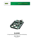
BL4S100
C-Programmable Single-Board Computer with Networking
User’s Manual
019–0172_C
BL4S100 User’s Manual
Part Number 019-0172_C • Printed in U.S.A.
©2008-2010 Digi International Inc. • All rights reserved.
Digi International reserves the right to make changes and
improvements to its products without providing notice.
Trademarks
Rabbit, RabbitCore, and Dynamic C are registered trademarks of Digi International Inc.
RabbitNet is a trademark of Digi International Inc.
The latest revision of this manual is available on the Rabbit Web site, www.rabbit.com,
for free, unregistered download.
Digi International Inc.
www.rabbit.com
TABLE OF CONTENTS
Chapter 1. Introduction
4
1.1 BL4S100 Description ...........................................................................................................................4
1.2 BL4S100 Features.................................................................................................................................4
1.3 Development and Evaluation Tools......................................................................................................6
1.3.1 Tool Kit .........................................................................................................................................6
1.3.2 Software ........................................................................................................................................7
1.3.3 Optional Add-Ons .........................................................................................................................7
1.4 CE Compliance .....................................................................................................................................8
1.4.1 Design Guidelines .........................................................................................................................9
1.4.2 Interfacing the BL4S100 to Other Devices...................................................................................9
Chapter 2. Getting Started
10
2.1 BL4S100 Connections ........................................................................................................................11
2.1.1 Hardware Reset ...........................................................................................................................12
2.2 Installing Dynamic C ..........................................................................................................................13
2.3 Starting Dynamic C ............................................................................................................................14
2.4 Run a Sample Program .......................................................................................................................14
2.4.1 Troubleshooting ..........................................................................................................................14
2.4.2 Run a ZigBee Sample Program (BL4S100/BL4S150 only) .......................................................15
2.5 Where Do I Go From Here? ...............................................................................................................16
Chapter 3. Subsystems
17
3.1 BL4S100 Pinouts ................................................................................................................................18
3.1.1 Connectors ..................................................................................................................................18
3.2 Digital I/O ...........................................................................................................................................19
3.2.1 Digital Inputs...............................................................................................................................19
3.2.2 Digital Outputs ............................................................................................................................22
3.3 Serial Communication ........................................................................................................................25
3.3.1 RS-232 ........................................................................................................................................25
3.3.2 Programming Port .......................................................................................................................25
3.3.3 Ethernet Port ...............................................................................................................................26
3.4 A/D Converter Inputs..........................................................................................................................27
3.4.1 A/D Converter Calibration..........................................................................................................29
3.5 USB Programming Cable ...................................................................................................................30
3.5.1 Changing Between Program Mode and Run Mode ....................................................................30
3.6 Other Hardware...................................................................................................................................31
3.6.1 Clock Doubler .............................................................................................................................31
3.6.2 Spectrum Spreader ......................................................................................................................31
3.7 Memory...............................................................................................................................................32
3.7.1 SRAM .........................................................................................................................................32
3.7.2 Flash Memory .............................................................................................................................32
3.7.3 VBAT RAM Memory .................................................................................................................32
BL4S100 User’s Manual
1
Chapter 4. Software
33
4.1 Running Dynamic C ...........................................................................................................................33
4.1.1 Upgrading Dynamic C ................................................................................................................35
4.1.2 Add-On Modules.........................................................................................................................35
4.2 Sample Programs ................................................................................................................................36
4.2.1 Digital I/O ...................................................................................................................................37
4.2.2 Serial Communication.................................................................................................................43
4.2.3 A/D Converter Inputs..................................................................................................................45
4.2.4 Real-Time Clock .........................................................................................................................46
4.2.5 TCP/IP Sample Programs ...........................................................................................................46
4.2.6 ZigBee Sample Programs............................................................................................................46
4.3 BL4S100 Libraries..............................................................................................................................47
4.4 BL4S100 Function Calls.....................................................................................................................48
4.4.1 Board Initialization .....................................................................................................................48
4.4.2 Digital I/O ...................................................................................................................................49
4.4.3 Rabbit RIO Interrupt Handlers....................................................................................................75
4.4.4 Serial Communication.................................................................................................................79
4.4.5 A/D Converter Inputs..................................................................................................................80
4.4.6 SRAM Use ..................................................................................................................................94
Chapter 5. Using the Ethernet TCP/IP Features
95
5.1 TCP/IP Connections ...........................................................................................................................95
5.2 TCP/IP Sample Programs ...................................................................................................................97
5.2.1 How to Set IP Addresses in the Sample Programs .....................................................................97
5.2.2 How to Set Up your Computer for Direct Connect ....................................................................98
5.2.3 Run the PINGME.C Demo ......................................................................................................99
5.2.4 Running More Demo Programs With a Direct Connection ......................................................100
5.3 Where Do I Go From Here? .............................................................................................................102
Chapter 6. Using the ZigBee Features
103
6.1 Introduction to the ZigBee Protocol .................................................................................................103
6.2 ZigBee Sample Programs .................................................................................................................104
6.2.1 Setting Up the Digi XBee USB Coordinator ............................................................................105
6.2.2 Setting up Sample Programs .....................................................................................................107
6.3 Dynamic C Function Calls................................................................................................................111
6.4 Where Do I Go From Here? .............................................................................................................111
Appendix A. Specifications
112
A.1 Electrical and Mechanical Specifications ........................................................................................113
A.1.1 Exclusion Zone.........................................................................................................................115
A.1.2 Headers.....................................................................................................................................115
A.2 Jumper Configurations.....................................................................................................................116
A.3 Use of Rabbit Microprocessor Parallel Ports...................................................................................118
Appendix B. Power Supply
120
B.1 Power Supplies.................................................................................................................................120
B.2 Batteries and External Battery Connections ....................................................................................121
B.2.1 Replacing the Backup Battery ..................................................................................................121
Appendix C. Demonstration Board
122
C.1 Connecting Demonstration Board....................................................................................................123
C.2 Demonstration Board Features.........................................................................................................124
C.2.1 Pinout........................................................................................................................................124
C.2.2 Configuration............................................................................................................................124
Appendix D. Rabbit RIO Resource Allocation
BL4S100 User’s Manual
126
2
D.1 Digital I/O Pin Associations ............................................................................................................127
D.2 Interpreting Error Codes ..................................................................................................................128
Appendix E. Plastic Enclosure
130
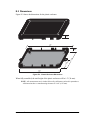
E.1 Assembly Instructions ......................................................................................................................131
E.2 Dimensions .......................................................................................................................................133
Appendix F. Additional Configuration Instructions
134
F.1 XBee Module Firmware Downloads ................................................................................................134
F.1.1 Dynamic C v. 10.44 and Later ..................................................................................................134
F.2 Digi® XBee USB Configuration ......................................................................................................135
F.2.1 Additional Reference Information ............................................................................................136
F.2.2 Update Digi® XBee USB Firmware .........................................................................................138
Index
139
Schematics
142
BL4S100 User’s Manual
3
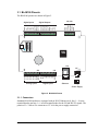
1. INTRODUCTION
The BL4S100 series of high-performance, C-programmable singleboard computers offers built-in RS-232, digital I/O and analog
inputs combined with Ethernet and ZigBee network connectivity
in a compact form factor. The BL4S100 single-board computers
are ideal for both discrete manufacturing and process-control
applications.
A Rabbit® 4000 microprocessor provides fast data processing.
1.1 BL4S100 Description
Throughout this manual, the term BL4S100 refers to the complete series of BL4S100 singleboard computers unless other production models are referred to specifically.
The BL4S100 is an advanced single-board computer that incorporates the powerful Rabbit
4000 microprocessor, serial flash memory, static RAM, digital inputs, digital outputs, A/D
converter inputs, RS-232 serial ports, and Ethernet and ZigBee network connectivity.
1.2 BL4S100 Features
• Rabbit® 4000 microprocessor operating at 40.00 MHz.
• Screw-terminal connectors
• 512KB SRAM (battery-backed), 512KB/1MB fast SRAM, and 1MB/2MB flash memory
options.
• 20 digital I/O: 12 protected digital inputs, and 8 sinking digital outputs.
• Advanced input capabilities including event counting, event capture, and quadrature
decoders that may be set up on all the digital input pins.
• Independent PWM and PPM capability on all the digital output pins.
• Eight 11-bit A/D converter inputs (plus one bit for sign).
• Ethernet and ZigBee network connectivity.
• Three serial ports:
Two 3-wire RS-232 serial ports or one 5-wire RS-232 serial port:
One serial port dedicated to programming/debugging.
BL4S100 User’s Manual
4
• Battery-backed real-time clock.
• Watchdog supervisor.
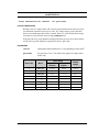
Four BL4S100 models are available. Their standard features are summarized in Table 1.
Table 1. BL4S100 Models
Feature
BL4S100
BL4S110
512KB
1MB
Data SRAM
512KB
Serial Flash Memory
(program)
1MB
2MB
A/D Converter
12 bits
Ethernet Interface
ZigBee Interface
BL4S160
Rabbit® 4000 running at 40.00 MHz
Microprocessor
Program Execution SRAM
BL4S150
10Base-T
ZigBee PRO
(802.15.4)
—
ZigBee PRO
(802.15.4)
—
BL4S100 single-board computers are programmed over a standard PC USB port through a
programming cable supplied with the Tool Kit.
NOTE: BL4S100 Series single-board computers cannot be programmed via the RabbitLink.
Appendix A provides detailed specifications.
Visit the Web site for up-to-date information about additional add-ons and features as
they become available. The Web site also has the latest revision of this user’s manual.
BL4S100 User’s Manual
5
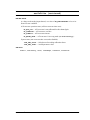
1.3 Development and Evaluation Tools
1.3.1 Tool Kit
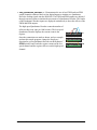
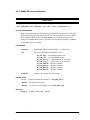
A Tool Kit contains the hardware essentials you will need to use your own BL4S100 singleboard computer. These items are supplied in the Tool Kit.
• Getting Started instructions.
• Dynamic C CD-ROM, with complete product documentation on disk.
• USB programming cable, used to connect your PC USB port to the BL4S100.
• Universal AC adapter, 12 V DC, 1 A (includes Canada/Japan/U.S., Australia/N.Z.,
U.K., and European style plugs).
• Demonstration Board with pushbutton switches and LEDs. The Demonstration Board
can be hooked up to the BL4S100 to demonstrate the I/O and capabilities of the
BL4S100.
• DB9 to bare leads serial cable.
• CAT 5/6 Ethernet crossover cable.
• Screwdriver.
• Rabbit 4000 Processor Easy Reference poster.
• Registration card.
•
•
•
•
•
•
•
•
•
•
set up.exe
Figure 1. BL4S100 Tool Kit
BL4S100 User’s Manual
6
1.3.2 Software
The BL4S100 is programmed using version 10.44 or later of Rabbit’s Dynamic C. A compatible version is included on the Tool Kit CD-ROM. This version of Dynamic C includes the
popular µC/OS-II real-time operating system, point-to-point protocol (PPP), FAT file
system, RabbitWeb, and other select libraries.
Rabbit also offers for purchase the Rabbit Embedded Security Pack featuring the Secure
Sockets Layer (SSL) and a specific Advanced Encryption Standard (AES) library. In addition to the Web-based technical support included at no extra charge, a one-year telephonebased technical support subscription is also available for purchase. Visit our Web site at
www.rabbit.com for further information and complete documentation, or contact your
Rabbit sales representative or authorized distributor.
1.3.3 Optional Add-Ons
Rabbit has a plastic enclosure and a Mesh Network Add-On Kit available for the
BL4S100.
• Mesh Network Add-On Kit (Part No. 101-1272)
Digi® XBee USB (used as ZigBee coordinator)
XBee Series 2 RF module
RF Interface module
The XBee Series 2 RF module is installed on the RF Interface module, which can be
connected via an RS-232 serial connection to a Windows PC for setup. The Mesh Network Add-On Kit enables you to explore the wireless capabilities of BL4S100 models
that offer a ZigBee network interface.
• Plastic enclosure (Part No. 181-0041)
RX TX/1W CTS
RTS
+5 V
GND
+K1
GND
OUT2 OUT1 OUT0 IN3
OUT7 OUT6 OUT5 OUT4 OUT3
IN2
IN1
IN0
+K
GND
AIN1
AIN2
AIN3
AIN4
AIN5
AIN6
AIN7 AGND
IN11
J13
L9
IN10
IN9
IN8
IN7
IN6
IN5
IN4
GND
RST
J6
R24
R30
U14
C13
U4
R28
R29
R51
C27
C38
C42
C43
C28
R25
R35
C3
L10
R56
R59
R44
R38
R40
R45
D1
J8
R41
R31
R43
R53
U10
C56
C45
C59
C66
C71
C48
U16
C73
C77
C72
C76
R71
U17
C79
C85
R75
U19
C94
R92
C113
R97
C112
2
8
7
J14
L3
D18
R85
L7
R11
6
R11
8
R76
C100
L11 R95 R96
R77
C70
C75
Y1
Y2 C55
C93
D27
4
J17
PWR
DS4
2
L12
S3
J16
S4
R11
7
L8
1
D10
C4
C12
C14
R37
C15
C16
D26
RP4
RP6
U21 C90
L4
D25
C11
0
D24
2
C11
4
D23
C10
9
D22
C25
R48U6R49C26
R50
C35
R52
1
C57
R55
R61
R58
Y3
R64
C67
2 R67
Y4 R68
R70
1
C84
R79
C98
R80
R78
C11
1
R81
L6L5
R82
C88 R83
C99 C89
R60
D21
2
C7
C11
D16
C36
R5
R4
R22
R21
R20
R19
R18
R17
U9
C23
C24
C21
C22
C19
C20
C17
C18
J12
C91
C92
R16
R15
R13
R12
R7
R8
R9
R10
ee
Ser
ies
2
XB
C108
C107
C106
C105
C104
C103
C102
C101
R99
R98
R105
R104
R103
R101
R100
R102
R111
R110
R113
R112
R109
R108
R107
R106
R14
J3
D20
RP3
RP5
U11
C39
C40
Q9
C52
DS3
AIN0
C31
C34
C51
R84
2
J15
JP1
C6
C10
C8
R27
R32
R36
R39
U5
C30
C33
3
R88
D19
GND
C29
R54
U12
J4
4
R57
C61
4
1
J1
D11
R42
R46
R47
C37 C32
R33
+K2
C81
C83
C80
C82
R94 R91
R115
S2
C62
C63
3
R66
C78
R86
ADC PROGRAMMER
S1
BT1
C53
C54
J5
ND
R65
C96
C95
C97
C47
C50
R62 U15
C60
8
R63
C86
C87
U20
R87
R89
R90
R93
1
C2
R6 U1
R23
C9
U3
R26 R34
C41
C44
7
AG
AIN3
AIN1
D17
L2
C65
C64
C68
C69
C74
R69
R72
R73
R74
U18
J10
2
1
AIN2
J11
2
1
C46
C49
J9
L1
C1
R2
D9
Q8
U8
U13
11
C58
D8
Q7
D7
Q6
C5
D15
U7
10
20
AIN0
D6
Q5
D5
Q4
U2
D14
2
RP2
D13
RNET
RP1
D4
Q3
R11
D12
3
D3
Q2
4
D2
Q1
J2 2
10
11
RNET
PWR
GN
D
J7
20
2
+5 V
BUTTON
DS1
DS2
R1
Further details on the plastic enclosure are provided in
Appendix E.
3
PWR
IN
Visit our Web site at www.rabbit.com or contact your Rabbit sales representative or
authorized distributor for further information.
BL4S100 User’s Manual
7
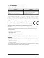
1.4 CE Compliance
Equipment is generally divided into two classes.
CLASS A
CLASS B
Digital equipment meant for light industrial use
Digital equipment meant for home use
Less restrictive emissions requirement:
less than 40 dB µV/m at 10 m
(40 dB relative to 1 µV/m) or 300 µV/m
More restrictive emissions requirement:
30 dB µV/m at 10 m or 100 µV/m
These limits apply over the range of 30–230 MHz. The limits are 7 dB higher for frequencies above 230 MHz. Although the test range goes to 1 GHz, the emissions from Rabbitbased systems at frequencies above 300 MHz are generally well below background noise
levels.
The BL4S100 single-board computer has been tested and was found to
be in conformity with the following applicable immunity and emission
standards. The BL4S110, BL4S150, and BL4S160 single-board
computers are also CE qualified as they are sub-versions of the BL4S100
single-board computer. Boards that are CE-compliant have the CE mark.
Immunity
The BL4S100 series of single-board computers meets the following EN55024/1998
immunity standards.
• EN61000-4-3 (Radiated Immunity)
• EN61000-4-4 (EFT)
• EN61000-4-6 (Conducted Immunity)
Additional shielding or filtering may be required for a heavy industrial environment.
Emissions
The BL4S100 series of single-board computers meets the following emission standards.
• EN55022:1998 Class B
• FCC Part 15 Class B
Your results may vary, depending on your application, so additional shielding or filtering
may be needed to maintain the Class B emission qualification.
BL4S100 User’s Manual
8
1.4.1 Design Guidelines
Note the following requirements for incorporating the BL4S100 series of single-board
computers into your application to comply with CE requirements.
General
• The power supply provided with the Tool Kit is for development purposes only. It is the
customer’s responsibility to provide a CE-compliant power supply for the end-product
application.
• When connecting the BL4S100 single-board computer to outdoor cables, the customer
is responsible for providing CE-approved surge/lighting protection.
• Rabbit recommends placing digital I/O or analog cables that are 3 m or longer in a
metal conduit to assist in maintaining CE compliance and to conform to good cable
design practices.
• When installing or servicing the BL4S100, it is the responsibility of the end-user to use
proper ESD precautions to prevent ESD damage to the BL4S100.
Safety
• All inputs and outputs to and from the BL4S100 series of single-board computers must
not be connected to voltages exceeding SELV levels (42.4 V AC peak, or 60 V DC).
• The lithium backup battery circuit on the BL4S100 single-board computer has been
designed to protect the battery from hazardous conditions such as reverse charging and
excessive current flows. Do not disable the safety features of the design.
1.4.2 Interfacing the BL4S100 to Other Devices
Since the BL4S100 series of single-board computers is designed to be connected to other
devices, good EMC practices should be followed to ensure compliance. CE compliance is
ultimately the responsibility of the integrator. Additional information, tips, and technical
assistance are available from your authorized Rabbit distributor, and are also available on
our Web site at www.rabbit.com.
BL4S100 User’s Manual
9
2. GETTING STARTED
Chapter 2 explains how to connect the programming cable and
power supply to the BL4S100.
BL4S100 User’s Manual
10
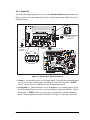
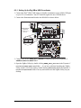
2.1 BL4S100 Connections
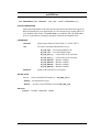
Step 1 — Connect Programming Cable
The programming cable connects the BL4S100 to the PC running Dynamic C to download
programs and to monitor the BL4S100 module during debugging.
Connect the 10-pin PROG connector of the programming cable to header J8 on the
BL4S100. Ensure that the colored edge lines up with pin 1 as shown. (Do not use the DIAG
connector, which is used for monitoring only.) Connect the other end of the programming
cable to an available USB port on your PC or workstation.
Programming
Cable
Colored
edge
RX TX/1W CTS
GND
IN1
IN0
+K
GND
RP6
1
J6
R30
R28
R29
C48
U17
C79
R77
C94
L10 L11 R95 R96
R92
C113
R97
C112
2
8
7
L3
D18
C90
U19
L7
C99
C89
Y2 C55
U16
C85
R85
U21
C111L6L5
C88
C98
C110
L9
C59
R75
R76
R58
R79
R80
R78
R81
R82
R83
S3
J16
J14
D27
4
DS3
DS4
IN11 IN10
IN9
IN8
IN7
IN6
IN5
IN4
GND
RST
C93
J17 2
S4
AIN0 AIN1 AIN2 AIN3 AIN4 AIN5 AIN6 AIN7 AGND
U10
R116
R118
R61
2
U14
R117
R55
L4
RP5
C36
R51
C27
C66
R71
C100
L8
R53
C56
C45
C73
C77
C72
C76
C71
C70
C75
C114
C108
R105
R113
C109
C107
R104
R112
J13
C106
D10
C4 C3
R4
R37
C16 C15 C14
U9
C23
C24
C21
C22
C19
C20
R60
C105
J12
C104
RP4
J15
C38
C42
C43
R7
R8
R9
R10
C17
C18
Series 2
C12
R5
R22
R21
R20
R19
R18
R17
R16
R15
R14
R13
R12
XBee
C103
C91
C92
C102
R103
R111
R99
R102
C101
R98
R101
R110
R100
R109
R108
C28
J3
R107
RP3
D26
R41
R31
R43
Y1
C57
To
PC USB port
J4
D25
R33
IN2
R106
J5
8
D24
R45
R38
L12
OUT2 OUT1 OUT0 IN3
GND OUT7 OUT6 OUT5 OUT4 OUT3
D23
R25
R35
+K1
2
GND
D22
R52
Q9
C67
R88
D21
R40
R50
J8
U4
1
2 R67
Y4 R68
R70
1
R94 R91
D1
C13
U12
+K2
C81
C83
C35
C39
C40
R59
Y3
R64
4
R24
R44
C25
R48U6R49
C26
U11 D16
R56
R84
R115
C34
3
C84
ADC PROGRAMMER
2
C30
C33
C51
1
C62
C63
3
3
S2
C60
C80
C82
D20
U5
C31
4
+5 V
BUTTON
AIN1
S1
AIN0
C29
C37 C32
R66
C78
D19
R42
R39
R46
R47
C52
R57
C61
4
2
C7
C11
R32
R36
C41
C44 R54
C53
C54
R62 U15
BT1
C96
C95
C97
7
1
C47
C50
R86
R87
R89
R90
R93
R27
J8
AIN3
JP1
C6
C10
C8
PROG
AGND
AIN2
C9
U13
C86
C87
U20
U18
J1
D11
U3
R26 R34
U8
D17
R63
R65
1
D15
U7
C46
C49
L2
C65
C64
C68
J11
2
C5
D14
J9
L1
C2
R6 U1
R23
PROG
10
1
D9
Q8
U2
11
C58
J10
2
D13
D12
20
C69
C74
R69
R72
R73
R74
C1
R2
D8
Q7
D7
Q6
R11
11
20
R1
D6
Q5
D5
Q4
RP2
RNET
D4
Q3
J2 2
D3
Q2
RNET
PWR
D2
Q1
10
DIAG
GND
J7
2
RTS +5 V
DS1
DS2
RP1
3
PWR
IN
PWR
Figure 2. Programming Cable Connections
Your PC should recognize the new USB hardware, and the LEDs in the shrink-wrapped
area of the USB programming cable will flash — if you get an error message, you will
have to install USB drivers. Drivers for Windows XP are available in the Dynamic C
Drivers\Rabbit USB Programming Cable\WinXP_2K folder — double-click
DPInst.exe to install the USB drivers. Drivers for other operating systems are available
online at www.ftdichip.com/Drivers/VCP.htm.
BL4S100 User’s Manual
11
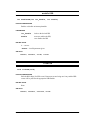
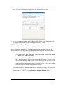
Step 2 — Connect Power Supply
Once all the other connections have been made, you can connect power to the BL4S100.
First, prepare the AC adapter for the country where it will be used by selecting the plug.
The Tool Kit presently includes Canada/Japan/U.S., Australia/N.Z., U.K., and European
style plugs. Snap in the top of the plug assembly into the slot at the top of the AC adapter
as shown in Figure 3, then press down on the spring-loaded clip below the plug assembly
to allow the plug assembly to click into place. Release the clip to secure the plug assembly
in the AC adapter.
Connect the power supply to header J17 on the BL4S100 as shown in Figure 3. Be sure to
match the latch mechanism with the top of the connector to header J17 on the BL4S100 as
shown. The Micro-Fit® connector will only fit one way.
Figure 3. Power Supply Connections
Plug in the AC adapter. The red LED next to the power connector at J17 should light up.
The BL4S100 is now ready to be used.
CAUTION: Unplug the power supply while you make or otherwise work with the connections
to the headers. This will protect your BL4S100 from inadvertent shorts or power spikes.
2.1.1 Hardware Reset
A hardware reset is done by unplugging the power supply, then plugging it back in, or by
pressing the RESET button located next to the Ethernet jack.
BL4S100 User’s Manual
12
2.2 Installing Dynamic C
If you have not yet installed Dynamic C version 10.44 (or a later version), do so now by
inserting the Dynamic C CD from the BL4S100 Tool Kit in your PC’s CD-ROM drive. If
autorun is enabled, the CD installation will begin automatically.
If autorun is disabled or the installation does not start, use the Windows Start | Run menu
or Windows Disk Explorer to launch setup.exe from the root folder of the CD-ROM.
The installation program will guide you through the installation process. Most steps of the
process are self-explanatory.
NOTE: If you have an earlier version of Dynamic C already installed, the default installation of the later version will be in a different folder, and a separate icon will appear on
your desktop.
The online documentation is installed along with Dynamic C, and an icon for the documentation menu is placed on the workstation’s desktop. Double-click this icon to reach the
menu. If the icon is missing, create a new desktop icon that points to default.htm in the
docs folder, found in the Dynamic C installation folder. The latest versions of all documents are always available for free, unregistered download from our Web sites as well.
The Dynamic C User’s Manual provides detailed instructions for the installation of
Dynamic C and any future upgrades.
Once your installation is complete, you will have up to three icons on your PC desktop.
One icon is for Dynamic C, one opens the documentation menu, and the third is for the
Rabbit Field Utility, a tool used to download precompiled software to a target system.
If you have purchased any of the optional Dynamic C modules, install them after installing
Dynamic C. The modules may be installed in any order. You must install the modules in
the same directory where Dynamic C was installed.
BL4S100 User’s Manual
13
2.3 Starting Dynamic C
Once the BL4S100 is connected to your PC and to a power source, start Dynamic C by
double-clicking on the Dynamic C icon on your desktop or in your Start menu. Select
Store Program in Flash on the “Compiler” tab in the Dynamic C Options > Project
Options menu. Then click on the “Communications” tab and verify that Use USB to
Serial Converter is selected to support the USB programming cable. Click OK.
You may have to select the COM port assigned to the USB programming cable on your
PC. In Dynamic C, select Options > Project Options, then select this COM port on the
“Communications” tab, then click OK. You may type the COM port number followed by
Enter on your computer keyboard if the COM port number is outside the range on the
dropdown menu.
2.4 Run a Sample Program
You are now ready to test your set-up by running a sample program.
Use the File menu to open the sample program PONG.C, which is in the Dynamic C
SAMPLES folder. Press function key F9 to compile and run the program. The STDIO
window will open on your PC and will display a small square bouncing around in a box.
This program shows that the CPU is working. The sample program described in
Section 5.2.3, “Run the PINGME.C Demo,” tests the TCP/IP portion of the board.
2.4.1 Troubleshooting
If you receive the message No Rabbit Processor Detected, the programming cable
may be connected to the wrong COM port, a connection may be faulty, or the target system may not be powered up. First, check to see that the red power LED next to header J5
is lit. If the LED is lit, check both ends of the programming cable to ensure that it is firmly
plugged into the PC and the programming header on the BL4S100 with the marked (colored) edge of the programming cable towards pin 1 of the programming header.
If Dynamic C appears to compile the BIOS successfully, but you then receive a communication error message when you compile and load a sample program, it is possible that your
PC cannot handle the higher program-loading baud rate. Try changing the maximum
download rate to a slower baud rate as follows.
• Locate the Serial Options dialog on the “Communications” tab in the Dynamic C
Options > Project Options menu. Select a slower Max download baud rate. Click OK
to save.
If a program compiles and loads, but then loses target communication before you can
begin debugging, it is possible that your PC cannot handle the default debugging baud
rate. Try lowering the debugging baud rate as follows.
• Locate the Serial Options dialog on the “Communications” tab in the Dynamic C
Options > Project Options menu. Choose a lower debug baud rate. Click OK to save.
Press <Ctrl-Y> to force Dynamic C to recompile the BIOS. You should receive a Bios
compiled successfully message once this step is completed successfully.
BL4S100 User’s Manual
14
2.4.2 Run a ZigBee Sample Program (BL4S100/BL4S150 only)
This section explains how to run a sample program in which the BL4S100/BL4S150 is used
in its default setup as a router and the Digi® XBee USB is used as the ZigBee coordinator.
1. Connect the Digi® XBee USB acting as a ZigBee coordinator to an available USB port
on your PC or workstation. Your PC should recognize the new USB hardware.
2. Find the file AT_INTERACTIVE.C, which is in the Dynamic C SAMPLES\XBee folder.
To run the program, open it with the File menu, then compile and run it by pressing F9.
The Dynamic C STDIO window will open to display a list of AT commands. Type
MENU to redisplay the menu of commands.
Waiting to join network...
done
Cmd - Description
=====================
ATCH - Read the current channel. Will be zero if we
are not associated with a network.
ATID - Set or read the current PAN ID. If you set the ID you
must write it to non-volitile memory ("WR") and
then reset the network software ("NR").
ATOP - Read the operating PAN ID.
ATMY - Read the current network address. Will be 0xFFFE
if we are not associated with a network.
ATSH - Read the upper four bytes of the radio IEEE address.
ATSL - Read the lower four bytes of the radio IEEE address.
ATNI - Set or read the Node Identifier.
ATBH - Set or read the maximum number of Broadcast Hops.
ATNT - Set or read the Node Discovery timeout value (in 0.1s).
ATSC - Set or read the list of channels to scan. This
value is a bit-field list.
ATSD - Set or read the channel scan duration value.
ATNJ - Set or read the Node Joining Time value.
ATAI - Read the Association Indicator. A zero value
means we are associated with a network.
ATPL - Set or read the transmission power level.
ATVR - Read the radio software version number.
ATHV - Read the radio hardware version number.
MENU - Display this menu (not an AT command.)
Valid command formats (AT prefix is optional, CC is command):
[AT]CC 0xXXXXXX (where XXXXXX is an even number of hexidecimal characters)
[AT]CC YYYY (where YYYY is an integer, up to 32 bits)
[AT]NI "Node ID String" (where quotes contain string data)
Enter AT Command:
Appendix F provides additional configuration information if you experience conflicts
while doing development simultaneously with more than one ZigBee coordinator, or if you
wish to upload new firmware.
BL4S100 User’s Manual
15
2.5 Where Do I Go From Here?
NOTE: If you purchased your BL4S100 through a distributor or Rabbit partner, contact
the distributor or partner first for technical support.
If there are any problems at this point:
• Use the Dynamic C Help menu to get further assistance with Dynamic C.
• Check the Rabbit Technical Bulletin Board and forums at www.rabbit.com/support/bb/
and at www.rabbit.com/forums/.
• Use the Technical Support e-mail form at www.rabbit.com/support/.
If the sample program ran fine, you are now ready to go on to explore other BL4S100
features and develop your own applications.
When you start to develop an application involving the analog inputs, run USERBLOCK_
READ_WRITE.C in the SAMPLES\UserBlock folder to save the factory calibration constants before you run any other sample programs in case you inadvertently write over
them while running another sample program.
Chapter 3, “Subsystems,” provides a description of the BL4S100’s features, Chapter 4,
“Software,” describes the Dynamic C software libraries and introduces some sample
programs, and Chapter 5, “Using the Ethernet TCP/IP Features,” explains the TCP/IP features.
BL4S100 User’s Manual
16
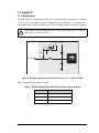
3. SUBSYSTEMS
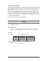
Chapter 3 describes the principal subsystems for the BL4S100.
• Digital I/O
• Serial Communication
• A/D Converter Inputs
• Memory
Figure 4 shows these Rabbit-based subsystems designed into the BL4S100.
BL4S100
Real-Time
Clock
Fast SRAM
(program)
Data
SRAM
Serial
Flash
Main
Clock
RABBIT ®
4000
Ethernet
Programming
Port
RS-232
RABBIT
RIO
®
ZigBee PRO
(802.15.4)
optional
Digital
Inputs
Digital
Outputs
A/D
Converter
Figure 4. BL4S100 Subsystems
BL4S100 User’s Manual
17
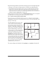
3.1 BL4S100 Pinouts
The BL4S100 pinouts are shown in Figure 5.
RS-232
GND
+K
IN0
IN1
IN2
IN3
OUT0
OUT1
OUT2
OUT3
OUT4
OUT5
OUT6
OUT7
GND
+K1
+K2
+5 V
J3
J4
GND
+5 V
TXF/RTS
RXF/CTS
TXD/1-W
RXD
Digital Outputs
Digital Inputs
RNET
Series 2
XBee
J5
Ethernet
GND
Digital Inputs
2
n.c.
IN11
IN10
IN9
IN8
IN7
IN6
IN5
IN4
GND
Analog Inputs
J17
4
2
3
1
n.c.
J16
+RAW
J15
AIN0
AIN1
AIN2
AIN3
AIN4
AIN5
AIN6
AIN7
AGND
J14
Power Supply
Figure 5. BL4S100 Pinouts
3.1.1 Connectors
Standard BL4S100 models are equipped with an RJ-45 Ethernet jack, four 1 × 9 screwterminal headers and one 1 × 6 screw-terminal header for the I/O and RS-232 signals. The
polarized 2 × 2 Micro-Fit® connector at J17 is for the power supply connection.
BL4S100 User’s Manual
18
3.2 Digital I/O
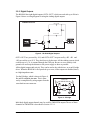
3.2.1 Digital Inputs
The BL4S100 has 12 digital inputs, IN0–IN11, each of which is protected over a range of
–36 V to +36 V. The inputs are factory-configured to be pulled up to +5 V, but they can
also be pulled up to +K or pulled down to 0 V by changing a jumper as shown in Figure 6.
CAUTION: Do not simultaneously jumper more than one setting when configuring
the pull-up or pull-down options.
J13
+K +5 V
+3.3 V
27 kW
IN0IN11
100 kW
Rabbit® RIO
Figure 6. BL4S100 Digital Inputs IN0–IN11 [Pulled Up to +5 V—Factory Default]
Table 2 summarizes the jumper settings.
Table 2. BL4S100 Digital Input Pull-Up/Pull-Down Jumper Settings
BL4S100 User’s Manual
Pins Jumpered
Pulled Up/Pulled Down
1–2
Inputs pulled up to +K
2–4 or 4–6
Inputs pulled down to GND
5–6
Inputs pulled up to +5 V
19
NOTE: If the inputs are pulled up to +K, the
voltage range over which the digital inputs are
protected changes to +K – 36 V to +36 V.
Normal Switching
Levels
+40 V
Digital Input Voltage
The actual switching threshold is approximately
1.40 V. Anything below this value is a logic 0,
and anything above 1.90 V is a logic 1. The
digital inputs are each fully protected over a
range of -36 V to +36 V, and can handle short
spikes of ±40 V.
Spikes
Spikes
+36 V
+3.3 V
40 V
Spikes
Figure 7. BL4S100 Digital Input
Protected Range
CAUTION: Do not allow the voltage on a digital input pin to exceed ±36 V to
avoid damaging the input.
Individual digital input channels may be also used for counters, synching, interrupts, input
capture, or as quadrature decoder inputs. The use of these channels for interrupts, input
capture, and as quadrature decoders is described below.
Blocks of digital input pins are associated with counters/timers on the Rabbit RIO chip.
Table 3 provides complete details for these associations.
Table 3. Counter/Timer Associations for BL4S100 Digital Input Pins
Configurable I/O
Pin(s)
Counter/Timer
Blocks
Block Shared
With
IN0–IN2
0
XBee RF module
IN3–IN5
1
—
IN6–IN7
2
OUT0–OUT1
IN8–IN9
3
OUT2–OUT3
IN10
6
—
IN11
7
—
Appendix D provides further details on the blocks and pins associated with the Rabbit
RIO chip to facilitate configuring each block consistently and to identify misconfigured
pins when a software function call returns a Mode Conflict error code.
BL4S100 User’s Manual
20
Keep the following guidelines in mind when selecting special uses for the digital input pins.
• Interrupts, event counters, and input capture are available on any digital input pin.
• Each Quadrature Decoder channel requires at least two digital input pins associated
with the same counter/timer block; three digital input pins associated with the same
counter/timer block are needed if you need indexing. Quadrature Decoder channels are
configured using the setDecoder() function call.
Sample programs in the DIO subdirectory in SAMPLES\BL4S1xx show how to set up and
use digital inputs for interrupts, pulse capture, and quadrature decoders.
3.2.1.1 Interrupt, Counter, and Event Capture Setup
External interrupts on the BL4S100 digital input pins are configured using the setExtInterrupt() function call. The interrupt can be set up to occur on a rising edge, a falling edge, or either edge.
An input channel may be set up to count
events, with the count incrementing or
decrementing, using the rising edge, falling edge, or either edge as triggers to start/
end the count. This feature is configured
using the setCounter() function call.
A more extensive use of the timing abilities
of the BL4S100 inputs can be realized
through the event capture function call,
setCapture(). Here the count of a particular clock cycle is noted at the start of the
event and at the end of the event so that the
time between them can be determined. This
can be set up on one or two input channels.
The event counter can be reset with the
resetCounter() function call.
Begin
Count
End
Count
Channel 0
Channel 1
Start
Event
End
Event
The counter readings can be obtained via the getBegin() or getEnd() function calls.
BL4S100 User’s Manual
21
3.2.2 Digital Outputs
The BL4S100 has eight digital outputs, OUT0–OUT7, which can each sink up to 200 mA.
Figure 8 shows a wiring diagram for using the sinking digital outputs.
SINKING OUTPUT
+K1 or +K2
OUT0OUT7
470 W
Rabbit® RIO
Figure 8. BL4S100 Digital Outputs
OUT0–OUT3 are powered by +K1, and OUT4–OUT7 are powered by +K2. +K1 and
+K2 can each be up to 36 V. They don't have to be the same. All the sinking current, which
could be up to 1.6 A, is returned through the GND pin. Be sure to use a suitably sized
ground wire and keep the distance to the power supply as short as possible.
All the digital outputs sink actively. They can be used as low-side drivers, or as an H-bridge
driver. When the BL4S100 is first powered up or reset, all the outputs are disabled, that is,
at a high-impedance state.
For the H bridge, which is shown in Figure 9,
Ka and Kb should be the same. This is most
easily accomplished by using outputs from the
same bank on one connector.
+Ka
+Kb
PULL-UP
RESISTORS
A
B
LOAD
B
A
Figure 9. H Bridge
Individual digital output channels may be used for PWM/PPM outputs.The use of these
channels for PWM/PPM is described in Section 3.2.2.1.
BL4S100 User’s Manual
22
Blocks of digital output pins are associated with counters/timers on the Rabbit RIO chip.
Table 4 provides complete details for these associations.
Table 4. Counter/Timer Associations for BL4S100 Digital Output Pins
Configurable I/O
Pin(s)
Counter/Timer
Blocks
Block Shared With
OUT0–OUT1
2
IN6–IN7
OUT2–OUT3
3
IN8–IN9
OUT4–OUT5
4
RabbitNet
(reserved for future use)
OUT6–OUT7
5
A/D converter
Appendix D provides further details on the blocks and pins associated with the Rabbit
RIO chip to facilitate configuring each block consistently and to identify misconfigured
pins when a software function call returns a Mode Conflict error code.
Keep the following guidelines in mind when selecting special uses for the digital output
pins.
• When using digital output pins for PWM/PPM outputs, the output pins can only share
the same RIO block if they are using the same period or frequency.
The PWM.C and the PPM.C sample programs in the DIO subdirectory in SAMPLES\
BL4S1xx show how to set up and use the PWM/PPM outputs.
BL4S100 User’s Manual
23
3.2.2.1 PWM/PPM Outputs Setup
A PWM output is described as noninverted
when it starts high, remains high for a duty
cycle that is a fraction of the period, then
goes low for the remainder of the period.
Similarly, an inverted PWM output starts
low, remains low for a duty cycle that is a
fraction of the period, then goes high for
the remainder of the period.
A PWM output is normally set up to start
when triggered by an event, and may be
set up so that the leading and trailing edges
of several PWM outputs are aligned as
long as the all the PWM outputs are on the
same block of a particular Rabbit RIO
chip.
A PPM ouput is similar to a PWM output,
except it is shifted by an offset relative to
the event that triggered the start of the
PPM output.
A PPM output is either inverted or noninverted, based on whether it starts high or
low, and may be set up so that their leading and trailing edges of several PPM outputs are aligned as long as the all the PPM
outputs are on the same block of a particular Rabbit RIO chip
PWM
OUTPUT
Period
Duty
Cycle
Noninverted
Inverted
PPM
OUTPUT
Period
Duty
Cycle
Offset
Shifted
PWM and PPM outputs on the BL4S100 are configured using the setPWM() and
setPPM() function calls.
BL4S100 User’s Manual
24
3.3 Serial Communication
The BL4S100 has two RS-232 serial ports, which can be configured as one RS-232 serial
channel (with RTS/CTS) or as two RS-232 (3-wire) channels using the serMode() software function call. Table 5 summarizes the options.
Table 5. Serial Communication Configurations
Serial Port
Mode
D
F
0
RS-232, 3-wire
RS-232, 3-wire
1
RS-232, 5-wire
CTS/RTS
The BL4S100 also has one CMOS serial channel that serves as the programming port.
All three serial ports operate in an asynchronous mode. An asynchronous port can handle
7 or 8 data bits. A 9th bit address scheme, where an additional bit is sent to mark the first
byte of a message, is also supported. Serial Port A, the programming port, can be operated
alternately in the clocked serial mode. In this mode, a clock line synchronously clocks the
data in or out. Either of the two communicating devices can supply the clock. The BL4S100
boards supports standard asynchronous baud rates up to 115,200 bps.
3.3.1 RS-232
The BL4S100 RS-232 serial communication is supported by an RS-232 transceiver. This
transceiver provides the voltage output, slew rate, and input voltage immunity required to
meet the RS-232 serial communication protocol. Basically, the chip translates the Rabbit
microprocessor’s CMOS signals to RS-232 signal levels. Note that the polarity is reversed
in an RS-232 circuit so that a +3.3 V output becomes approximately -10 V and 0 V is output as +10 V. The RS-232 transceiver also provides the proper line loading for reliable
communication.
RS-232 can be used effectively at the BL4S100’s maximum baud rate for distances of up
to 15 m.
3.3.2 Programming Port
The BL4S100 has a 10-pin programming header. The programming port uses the Rabbit
4000 Serial Port A for communication, and is used for the following operations.
• Programming/debugging
• Cloning
The programming port is used to start the BL4S100 in a mode where the BL4S100 will
download a program and then execute the program. The programming port transmits
information to and from a PC while a program is being debugged.
The Rabbit 4000 startup-mode pins (SMODE0, SMODE1) are presented to the programming port so that an externally connected device can force the BL4S100 to start up in an
BL4S100 User’s Manual
25
external bootstrap mode. The BL4S100 can be reset from the programming port via the
/RESET_IN line.
The Rabbit microprocessor status pin is also presented to the programming port. The status
pin is an output that can be used to send a general digital signal.
NOTE: Refer to the Rabbit 4000 Microprocessor User’s Manual for more information
related to the bootstrap mode.
3.3.3 Ethernet Port
Figure 10 shows the pinout for the Ethernet port (J4). Note that there are two standards for
numbering the pins on this connector—the convention used here, and numbering in reverse
to that shown. Regardless of the numbering convention followed, the pin positions relative
to the spring tab position (located at the bottom of the RJ-45 jack in Figure 10) are always
absolute, and the RJ-45 connector will work properly with off-the-shelf Ethernet cables.
ETHERNET
1
8
1.
2.
3.
6.
RJ-45 Plug
E_Tx+
E_Tx
E_Rx+
E_Rx
RJ-45 Jack
Figure 10. RJ-45 Ethernet Port Pinout
Two LEDs on the RJ-45 Ethernet jack indicate an Ethernet link (green LNK) and Ethernet
activity (yellow ACT).
The grounded RJ-45 connector is shielded to minimize EMI effects to/from the Ethernet
signals.
BL4S100 User’s Manual
26
3.4 A/D Converter Inputs
The single A/D converter chip used in the BL4S100 has a resolution of 12 bits (11 bits for
the value and one bit for the polarity). The A/D converter chip has a programmable-gain
amplifier. Each external input has circuitry that provides scaling and filtering. All 8 external
inputs are scaled and filtered to provide the user with an input impedance of 1 M and a
variety of single-ended unipolar, and differential bipolar ranges as shown in Table 6.
Figure 11 shows a pair of A/D converter input circuits. The resistors form an approx. 10:1
attenuator, and the capacitors filter noise pulses from the A/D converter inputs.
ADC
953 kW
AIN0
10 pF
105 kW
10 pF
105 kW
953 kW
AIN1
AGND
Figure 11. Buffered A/D Converter Inputs
The A/D converter chip can only accept positive voltages. By pairing the analog inputs,
differential bipolar measurements are possible, and can be configured for each channel pair
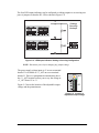
with the opmode parameter in the anaInConfig() software function call. The available
voltage ranges are listed in Table 6.
BL4S100 User’s Manual
27
Table 6. A/D Converter Input Voltage Ranges
Amplifier
Voltage Range
Gain
Single-Ended
Unipolar
Differential
Bipolar
1
0–20 V
± 20 V
2
0–10 V
± 10 V
4
0–5 V
±5V
5
0–4 V
±4V
8*
0–2.5 V
± 2.5 V
10
0–2 V
±2V
16
0–1.25 V
± 1.25 V
20
0–1 V
±1V
* 4–20 mA operation is available with an amplifier gain of 8
In the differential mode, each individual channel is limited to half the total voltage—for
example, the range for a gain code of 1 is ±20 V, but each channel is limited to 0–20 V.
Note that while the differential bipolar mode can return a negative value, this negative
value can only indicate negative with respect to the two differential voltages since the A/D
converter cannot handle a voltage below -0.2 V.
When using channels AIN0–AIN3 for current
measurements, remember to set the corresponding jumper(s) on headers J10 and J11.
The current measurements are realized by actually measuring the voltage drop across a 100
resistor.
AIN0
J11
Apply jumpers
for factory-default
current measurements
AIN1
AIN2
AIN3
J10
100 W
Figure 12. Analog Current Measurements
The A/D converter inputs are factory-calibrated, and the calibration constants are stored in
the user block.
BL4S100 User’s Manual
28
3.4.1 A/D Converter Calibration
When you start to develop your application, run USERBLOCK_READ_WRITE.C in the
SAMPLES\UserBlock folder to save the factory calibration constants in case you inadvertently write over them while running the sample programs.
To get the best results from the A/D converter, it is necessary to calibrate each mode
(single-ended, differential, and current) for each of its gains. It is imperative that you calibrate each of the A/D converter inputs in the same manner as they are to be used in the
application. For example, if you will be performing floating differential measurements or
differential measurements using a common analog ground, then calibrate the A/D converter in the corresponding manner. The calibration table in software only holds calibration constants based on mode, channel, and gain. Other factors affecting the calibration must
be taken into account by calibrating using the same mode and gain setup as in the intended use.
Sample programs are provided to illustrate how to read and calibrate the various A/D
inputs for the three operating modes.
Mode
Read
Calibrate
Single-Ended, unipolar
ADC_RD_SE_UNIPOLAR.C ADC_CAL_SE_UNIPOLAR.C
Differential, bipolar
ADC_RD_DIFF.C
ADC_CAL_DIFF.C
4–20 mA
ADC_RD_MA.C
ADC_CAL_MA.C
These sample programs are found in the ADC subdirectory in SAMPLES\BL4S1xx. See
Section 4.2.3 for more information on these sample programs and how to use them.
BL4S100 User’s Manual
29
3.5 USB Programming Cable
The USB programming cable is used to connect the serial programming port of the
BL4S100 to a PC USB port. The programming cable converts the voltage levels used by
the PC USB port to the CMOS voltage levels used by the Rabbit microprocessor.
When the PROG connector on the programming cable is connected to the programming
header on the BL4S100, programs can be downloaded and debugged over the serial interface.
The DIAG connector of the programming cable may be used on the programming header on
the BL4S100 with the BL4S100 operating in the Run Mode. This allows the programming
port to be used as a regular serial port.
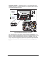
3.5.1 Changing Between Program Mode and Run Mode
The BL4S100 is automatically in Program Mode when the PROG connector on the programming cable is attached, and is automatically in Run Mode when reset with no programming cable is attached or the DIAG connector is attached. When the Rabbit microprocessor
is reset, the operating mode is determined by the status of the SMODE pins. When the programming cable’s PROG connector is attached, the SMODE pins are pulled high, placing
the Rabbit microprocessor in the Program Mode. When the programming cable’s PROG
connector is not attached, the SMODE0 pin is pulled low and the SMODE1 pin is high so
that the Rabbit 4000 powers up in the clocked serial bootstrap mode to load the program
from the serial flash when the BL4S100 is operating in the Run Mode.
Program Mode
Programming
Cable
Colored
edge
J6
R92
C113
R97
C112
8
7
L3
J14
D27
Run Mode
IN8
IN7
IN6
IN5
IN4
GND
RST
C93
4
J17 2
DS3
IN9
R33
C94
2
D18
C90
L7
L10 L11 R95 R96
DS4
IN11 IN10
R25
R35
R30
R28
R29
U17
U19
S4
AIN0 AIN1 AIN2 AIN3 AIN4 AIN5 AIN6 AIN7 AGND
U12
C36
C28
R51
C27
C66
C48
L12
S3
J16
U10
R77
R79
R80
R78
R81
R82
R83
C98
L4
C109
C110
L9
C114
1
R85
R117
R55
R61
J13
2
J15
RP6
C38
C42
C43
C23
C24
R58
R60
J12
C108
R105
R113
D10
C4 C3
R37
C16 C15 C14
C21
C22
U9
C19
C20
C12
R5
R22
R21
R20
R19
R18
R17
R16
R15
R14
R13
R12
R7
R8
R9
R10
C17
C18
Series 2
C107
C91
C92
C57
To
PC USB port
XBee
C106
C104
C105
C103
R104
C102
R103
R111
R112
R99
C101
R98
R102
RP5
R53
R75
R76
C100
L8
R41
R31
R43
U16
C79
C85
U21
GND
J3
R101
R71
C89
+K
R100
D26
RP4
C59
Y1
Y2 C55
C73
C77
C72
C76
C71
C70
C75
C99
IN0
R110
C67
C111L6L5
C88
IN1
R109
D25
R45
R38
C56
C45
U14
R116
R118
IN2
J4
R108
R4
OUT2 OUT1 OUT0 IN3
GND OUT7 OUT6 OUT5 OUT4 OUT3
R107
8
2
+K1
D24
3
+K2
D23
4
S2
D22
R52
2
+5 V
BUTTON
S1
2
R115
D21
C39
C40
R50
Q9
R84
RP3
C35
J8
U4
R44
C25
R48U6R49
C26
U11 D16
R56
2 R67
Y4 R68
R70
R94 R91
D1
C13
1
1
R88
GND
J5
R106
GND
AIN1
C34
R59
Y3
R64
C84
D20
C31
3
4
C81
C83
C80
C82
D19
U5
C30
C33
C51
1
3
R66
C78
ADC PROGRAMMER
7
AIN0
C29
R24
R40
R39
R46
R47
C52
C62
C63
2
C7
C11
R32
R36
R42
C41
C44 R54
R57
C61
4
C53
C54
C60
BT1
C96
C95
C97
RTS +5 V
AIN3
1
R27
C37 C32
R86
R87
R89
R90
R93
JP1
C6
C10
C8
U13
C47
C50
C46
C49
R62 U15
C86
C87
U20
U18
RNET
AGND
AIN2
R63
R65
1
U8
J1
D11
U3
R26 R34
D15
U7
D17
L2
C65
C64
C68
J11
2
D14
C9
PROG
10
R6 U1
R23
C5
J9
L1
1
C2
U2
11
C58
J10
2
D13
D12
20
C69
C74
R69
R72
R73
R74
C1
R2
D9
Q8
J2 2
RP2
D8
Q7
D7
Q6
R11
11
20
R1
D6
Q5
D5
Q4
RNET
PWR
10
D4
Q3
DIAG
GND
J7
D3
Q2
RX TX/1W CTS
DS1
DS2
RP1
D2
Q1
3
PWR
IN
PWR
RESET
DIAG
Power
PROG
RESET BL4S100 when changing mode:
Cycle power off/on or press RESET
after removing or attaching programming cable.
Figure 13. BL4S100 Program Mode and Run Mode Setup
A program “runs” in either mode, but can only be downloaded and debugged when the
BL4S100 is in the Program Mode.
Refer to the Rabbit 4000 Microprocessor User’s Manual for more information on the programming port and the programming cable.
BL4S100 User’s Manual
30
3.6 Other Hardware
3.6.1 Clock Doubler
The BL4S100 takes advantage of the Rabbit microprocessor’s internal clock doubler. A
built-in clock doubler allows half-frequency crystals to be used to reduce radiated emissions.
The clock doubler may be disabled if the higher clock speeds are not required. Disabling
the clock doubler will reduce power consumption and further reduce radiated emissions.
The clock doubler is disabled with a simple configuration macro as shown below.
1. Select the “Defines” tab from the Dynamic C Options > Project Options menu.
2. Add the line CLOCK_DOUBLED=0 to always disable the clock doubler.
The clock doubler is enabled by default, and usually no entry is needed. If you need to
specify that the clock doubler is always enabled, add the line CLOCK_DOUBLED=1 to
always enable the clock doubler.
3. Click OK to save the macro. The clock doubler will now remain off or on according to
your setting whenever you are using the project file where you defined the macro.
3.6.2 Spectrum Spreader
The Rabbit microprocessors features a spectrum spreader, which help to mitigate EMI
problems. By default, the spectrum spreader is on automatically, but it may also be turned
off or set to a stronger setting. The means for doing so is through a simple configuration
macro as shown below.
1. Select the “Defines” tab from the Dynamic C Options > Project Options menu.
2. Normal spreading is the default, and usually no entry is needed. If you need to specify normal spreading, add the line
ENABLE_SPREADER=1
For strong spreading, add the line
ENABLE_SPREADER=2
To disable the spectrum spreader, add the line
ENABLE_SPREADER=0
NOTE: The strong spectrum-spreading setting is not recommended since it may limit
the maximum clock speed or the maximum baud rate. It is unlikely that the strong setting will be used in a real application.
3. Click OK to save the macro. The spectrum spreader will be set according to the macro
value whenever a program is compiled using this project file.
NOTE: Refer to the Rabbit 4000 Microprocessor User’s Manual for more information
on the spectrum-spreading settings and the maximum clock speed.
BL4S100 User’s Manual
31
3.7 Memory
3.7.1 SRAM
All BL4S100 boards have 512KB of battery-backed data SRAM, and 512KB–1MB of fast
program execution SRAM.
3.7.2 Flash Memory
BL4S100 boards have 1MB—2MB of serial flash memory.
Writing to arbitrary flash memory addresses at run time is also discouraged. Instead,
define a “user block” area to store persistent data. The functions writeUserBlock()
and readUserBlock() are provided for this.
3.7.3 VBAT RAM Memory
The tamper detection feature of the Rabbit microprocessor can be used to detect any
attempt to enter the bootstrap mode. When such an attempt is detected, the VBAT RAM
memory in the Rabbit microprocessor is erased. The serial bootloader on the BL4S100
boards uses the bootstrap mode to load the SRAM, which erases the VBAT RAM memory
on any reset, and so it cannot be used for tamper detection.
BL4S100 User’s Manual
32
4. SOFTWARE
Dynamic C is an integrated development system for writing
embedded software. It runs on an IBM-compatible PC and is
designed for use with single-board computers and other devices
based on the Rabbit microprocessor.
Chapter 4 provides the libraries, function calls, and sample programs related to the BL4S100.
4.1 Running Dynamic C
Since the BL4S100 has a serial flash memory, all software development must be done in
the static SRAM. The flash memory and SRAM options are selected with the Options >
Program Options > Compiler menu. Select Store Program in Flash on the “Compiler”
tab for the program to run normally.
For debugging purposes, you may select Store Program in RAM on the “Compiler” tab
so that download speed is as fast as possible. Note that programs stored in RAM will be
lost when the BL4S100 is reset, so this option should be used only for debugging.
Developing software with Dynamic C is simple. Users can write, compile, and test C and
assembly code without leaving the Dynamic C development environment. Debugging
occurs while the application runs on the target. Alternatively, users can compile a program
to an image file for later loading. Dynamic C runs on PCs under Windows NT and later—
see Rabbit’s Technical Note TN257, Running Dynamic C® With Windows Vista®, for
additional information if you are using a Dynamic C under Windows Vista. Programs can
be downloaded at baud rates of up to 460,800 bps after the program compiles.
BL4S100 User’s Manual
33
Dynamic C has a number of standard features:
• Full-feature source and/or assembly-level debugger, no in-circuit emulator required.
• Royalty-free TCP/IP stack with source code and most common protocols.
• Hundreds of functions in source-code libraries and sample programs:
Exceptionally fast support for floating-point arithmetic and transcendental functions.
RS-232 and RS-485 serial communication.
Analog and digital I/O drivers.
I2C, SPI, GPS, file system.
LCD display and keypad drivers.
• Powerful language extensions for cooperative or preemptive multitasking
• Loader utility program to load binary images into Rabbit targets in the absence of
Dynamic C.
• Provision for customers to create their own source code libraries and augment on-line
help by creating “function description” block comments using a special format for
library functions.
• Standard debugging features:
Breakpoints—Set breakpoints that can disable interrupts.
Single-stepping—Step into or over functions at a source or machine code level, µC/OS-II aware.
Code disassembly—The disassembly window displays addresses, opcodes, mnemonics, and
machine cycle times. Switch between debugging at machine-code level and source-code level by
simply opening or closing the disassembly window.
Watch expressions—Watch expressions are compiled when defined, so complex expressions
including function calls may be placed into watch expressions. Watch expressions can be updated
with or without stopping program execution.
Register window—All processor registers and flags are displayed. The contents of general registers
may be modified in the window by the user.
Stack window—shows the contents of the top of the stack.
Hex memory dump—displays the contents of memory at any address.
STDIO window—printf outputs to this window and keyboard input on the host PC can be
detected for debugging purposes. printf output may also be sent to a serial port or file.
BL4S100 User’s Manual
34
4.1.1 Upgrading Dynamic C
4.1.1.1 Patches and Updates
Dynamic C patches that focus on bug fixes and updates are available from time to time.
Check the Web site at www.rabbit.com/support/ for the latest patches, workarounds, and
updates.
The default installation of a patch or update is to install the file in a directory (folder)
different from that of the original Dynamic C installation. Rabbit recommends using a
different directory so that you can verify the operation of the patch or update without overwriting the existing Dynamic C installation. If you have made any changes to the BIOS or
to libraries, or if you have programs in the old directory (folder), make these same changes
to the BIOS or libraries in the new directory containing the patch. Do not simply copy
over an entire file since you may overwrite an update; of course, you may copy over any
programs you have written. Once you are sure the new patch or update works entirely to
your satisfaction, you may retire the existing installation, but keep it available to handle
legacy applications.
4.1.2 Add-On Modules
Starting with Dynamic C version 10.40, Dynamic C includes the popular µC/OS-II realtime operating system, point-to-point protocol (PPP), FAT file system, RabbitWeb, and
other select libraries. Rabbit also offers for purchase the Rabbit Embedded Security Pack
featuring the Secure Sockets Layer (SSL) and a specific Advanced Encryption Standard
(AES) library.
In addition to the Web-based technical support included at no extra charge, a one-year
telephone-based technical support subscription is also available for purchase.
Visit our Web site at www.rabbit.com for further information and complete documentation.
BL4S100 User’s Manual
35
4.2 Sample Programs
Sample programs are provided in the Dynamic C Samples folder. The sample program
PONG.C demonstrates the output to the STDIO window.
The various directories in the Samples folder contain specific sample programs that illustrate the use of the corresponding Dynamic C libraries.
The SAMPLES\BL4S1xx folder provides sample programs specific to the BL4S100. Each
sample program has comments that describe the purpose and function of the program. Follow the instructions at the beginning of the sample program.
To run a sample program, open it with the File menu (if it is not still open), then compile
and run it by pressing F9. The BL4S100 must be in Program mode (see Section 3.5,
“USB Programming Cable,”) and must be connected to a PC using the programming cable
as described in Section 2.1, “BL4S100 Connections.” See Appendix C for information on
the power-supply connections to the Demonstration Board.
Complete information on Dynamic C is provided in the Dynamic C User’s Manual.
TCP/IP specific functions are described in the Dynamic C TCP/IP User’s Manual, which
is included in the online documentation set. Information on using the TCP/IP features and
sample programs is provided in Chapter 5, “Using the Ethernet TCP/IP Features.”
ZigBee specific functions are described in An Introduction to ZigBee, which is included
in the online documentation set. Information on using the TCP/IP features and sample programs is provided in Chapter 6, “Using the ZigBee Features.”
BL4S100 User’s Manual
36
4.2.1 Digital I/O
The following sample programs are found in the SAMPLES\BL4S1xx\DIO subdirectory.
Figure 14 shows the signal connections for the sample programs that illustrate the use of
the digital inputs.
JP15
DIGITAL INPUTS IN0IN11
HEADERS J3 & J4
BL4S100
J4
RX TX/1W CTS
RTS +5 V
+5 V
BUTTON
+K2
+K1
OUT2 OUT1 OUT0 IN3
GND OUT7 OUT6 OUT5 OUT4 OUT3
IN2
IN1
IN0
+K
GND
DS1
RNET
DS2
D26
2
RP6
1
L9
J6
U21
C94
R92
C113
R97
C112
2
8
7
L3
J14
D27
IN9
IN8
IN7
IN6
IN5
IN4
GND
RST
C93
4
J17 2
DS3
DS4
IN11 IN10
R33
R77
L7
L10 L11 R95 R96
S4
AIN0 AIN1 AIN2 AIN3 AIN4 AIN5 AIN6 AIN7 AGND
R25
R35
R30
R28
R29
C36
U17
U19
R116
R118
C90
R85
C99
C89
C48
R75
R76
C111L6L5
C88
C98
S3
J16
U10
U16
C79
C85
C100
L8
C114
RP5
J15
C38
C42
C43
C66
R71
R79
R80
R78
R81
R82
R83
RP4
C59
C73
C77
C72
C76
C71
C70
C75
Y1
Y2 C55
D18
D25
R53
C56
C45
L12
D24
R41
R31
R43
R45
R38
U12
R37
C28
R51
C27
C67
2 R67
Y4 R68
R70
L4
D23
R52
Q9
1
C109
C108
R105
R113
D22
R50
U14
R117
R55
R61
R58
Y3
R64
C110
C107
R104
R112
GND
D21
J13
C106
2
R115
D20
RP3
C39
C40
R56
C57
R60
C105
D10
C4 C3
C12
R5
C16 C15 C14
U9
C23
C24
C17
C18
C104
ADC PROGRAMMER
C35
J8
U4
R44
C25
R48U6R49
C26
U11 D16
R59
R88
D19
J12
C103
C91
C92
C102
R103
R111
R99
R102
C101
R98
R101
R110
R4
R22
R21
R20
R19
R18
R17
R16
R15
C21
C22
Series 2
C19
C20
XBee
R14
R13
R12
R7
R8
R9
R10
C62
C63
4
R94 R91
R100
R109
C34
D1
C13
1
R84
R108
AIN1
C31
3
C84
C96
U5
C30
C33
C51
1
3
C81
C83
C80
C82
R107
AIN0
C29
R24
R40
R39
R46
R47
C52
R66
C78
2
C7
C11
R32
R36
R42
C41
C44 R54
R57
C61
4
C53
C54
C60
BT1
R106
1
R27
C37 C32
R86
C95
C97
8
AIN3
2
AIN2
JP1
C6
C10
C8
U13
C47
C50
C46
C49
R62 U15
C86
C87
U20
R87
R89
R90
R93
J1
D11
C9
U3
3
J3
1
U8
D17
R63
U18
R6 U1
R23
R26 R34
D15
U7
10
R65
J11
2
D14
L2
C65
C64
C68
AGND
J10
2
D13
J9
L1
C2
U2
11
C58
1
D9
Q8
C5
D12
20
C69
C74
R69
R72
R73
R74
D8
Q7
D7
Q6
R11
11
20
C1
R2
D6
Q5
D5
Q4
RP2
4
J4
D4
Q3
S2
D3
Q2
S1
D2
Q1
10
J5
J7
7
GND
JP2
J2 2
R1
JP1
RP1
2
GND
J3
RNET
PWR
DEMO BOARD
POWER
CONNECT TO
BL4S100
HEADER J4
3
PWR
IN
PWR
Figure 14. Digital Inputs Signal Connections
• DIGIN.C—Demonstrates the use of the digital inputs. Using the Demonstration Board,
you can see an input channel toggle from HIGH to LOW in the Dynamic C STDIO
window when you press a pushbutton on the Demonstration Board.
• DIGIN_BANK.C—Demonstrates the use of digInBank() to read digital inputs. Using
the Demonstration Board, you can see an input channel toggle from HIGH to LOW in
the Dynamic C STDIO window when you press a pushbutton on the Demonstration
Board. The banking functions allow I/O banks to be input or output more efficiently.
BL4S100 User’s Manual
37
Figure 15 shows the signal connections for the sample programs that illustrate the use of
the digital outputs.
JP15
to GND
on
Header J4
J4
+5 V
BUTTON
+K2
+K1
OUT2 OUT1 OUT0 IN3
GND OUT7 OUT6 OUT5 OUT4 OUT3
IN2
IN1
IN0
+K
GND
DS1
RNET
DS2
D26
2
J15
RP6
1
S3
J16
R92
C113
R97
C112
2
8
7
J6
D27
IN8
IN7
IN6
IN5
IN4
GND
RST
C93
4
J17 2
DS3
IN9
R33
L3
J14
DS4
IN11 IN10
U12
R116
R118
C94
L10 L11 R95 R96
S4
AIN0 AIN1 AIN2 AIN3 AIN4 AIN5 AIN6 AIN7 AGND
R25
R35
R30
R28
R29
C36
R77
U19
L7
C99
C89
C90
R85
U21
C98
U17
R75
R76
C111L6L5
C88
L9
C48
U16
C79
C85
C100
L8
C114
RP5
C38
C42
C43
C66
R71
R79
R80
R78
R81
R82
R83
RP4
U10
D18
D25
C59
C73
C77
C72
C76
C71
C70
C75
Y2 C55
L12
D24
C109
D23
C110
D22
R53
C56
C45
U14
R117
R55
R61
R58
C67
2 R67
Y4 R68
R70
1
L4
GND
D21
J13
C108
R105
R115
D20
RP3
R52
R41
R31
R43
R45
R38
1
C57
R60
C107
R104
D10
C4 C3
R37
C16 C15 C14
U9
C23
C24
C21
C22
C19
C20
C17
C18
C106
C28
R7
R8
R9
R10
Series 2
C12
R5
R22
R21
R20
R19
R18
R17
R16
R15
R14
R13
R12
XBee
C105
J12
2
R113
C104
R112
C103
C91
C92
C102
R103
R111
C101
D19
C35
C39
C40
J8
U4
Y1
R88
ADC PROGRAMMER
D1
C13
R40
R50
Q9
C51
Y3
R64
4
C81
C83
R94 R91
R99
C34
R24
R44
C25
R48U6R49
C26
U11 D16
R56
R84
R102
R98
C30
C33
3
C84
R101
U5
C31
R59
1
3
R66
C78
C80
C82
R100
R110
R109
R108
R4
J3
R107
R32
R36
R42
R51
C27
J4
R106
C29
C37 C32
C62
C63
2
C7
C11
R39
R46
R47
C52
C60
BT1
C96
J5
R27
C41
C44 R54
R57
C61
4
C53
C54
R86
C95
C97
8
AIN1
C47
C50
R62 U15
C86
C87
U20
R87
R89
R90
R93
JP1
C6
C10
C8
U13
D17
R63
2
AIN0
U3
R26 R34
U8
J1
D11
C9
3
AIN3
R6 U1
R23
4
AIN2
1
D15
U7
C46
C49
L2
U18
J11
2
D14
10
R65
1
D13
J9
C65
C64
C68
AGND
J10
2
C69
C74
R69
R72
R73
R74
C2
U2
11
L1
1
D9
Q8
C5
D12
20
C58
S2
RP2
D8
Q7
D7
Q6
R11
11
20
C1
R2
D6
Q5
D5
Q4
S1
10
D4
Q3
7
GND
J7
D3
Q2
J2 2
R1
RP1
D2
Q1
2
J3
GND
DEMO BOARD
POWER
RTS +5 V
JP2
RX TX/1W CTS
JP1
OUT0
OUT1
OUT2
OUT3
RNET
PWR
DIGITAL OUTPUTS
OUT0OUT3
HEADERS J3 & J4
BL4S100
3
PWR
IN
PWR
Figure 15. Digital Outputs Signal Connections
• DIGOUT.C—Demonstrates the use of the sinking digital outputs. Using the Demonstration Board, you can see an LED toggle on/off via a sinking output that you selected via
the Dynamic C STDIO window.
• DIGOUT_BANK.C—Demonstrates the use of digOutBank() to control the sinking
digital outputs. Using the Demonstration Board, you can see an LED toggle on/off via a
sinking output that you selected via the Dynamic C STDIO window. The banking functions allow I/O banks to be input or output more efficiently.
BL4S100 User’s Manual
38
• INTERRUPTS.C—Demonstrates the use of the Rabbit RIO interrupt service capabilities.
Set up the Demonstration Board as shown in Figure 14 with IN0 connected to SW1.
The sample program sets up two interrupt sources, an external interrupt tied to pushbutton
switch SW1, and a rollover interrupt tied to a timer that is producing a PWM output.
The Dynamic C STDIO window will show a count of rollovers that have occurred since
the PWM signal was started. The window will also display Button Pressed each time
the pushbutton switch is pressed. Each time the button is pressed, the timeout timer that
removes the message is reset, so you can keep the message on the screen indefinitely by
pressing the button repeatedly.
• PPM.C—Demonstrates the use of up to eight PPM channels on the digital output pins
on headers J3 and J4. The PPM signals are set for a frequency of 200 Hz, with the duty
cycle adjustable from 0 to 100% and an offset adjustable from 0 to 100% by the user.
These pins can be connected to an oscilloscope to view the waveform being generated.
The overall frequency can be adjusted in the #define PPM_FREQ line. Follow these
instructions when running this sample program.
1. The digital outputs on the BL4S100 do not have an internal pull-up resistor and will not register on
the oscilloscope without a pull-up resistor. The Demonstration Board has pull-up resistors—
connect OUT0–OUT3 on the BL4S100 to SW1–SW4 on header J1 of the Demonstration Board.
2. Connect the oscilloscope probe to digital output pins OUT0–OUT3 on headers J3 or J4. Remember
to connect the oscilloscope ground to GND on header J4.
Once you compile and run the sample program, change the duty cycle and offsets for a
given PPM channel via the Dynamic C STDIO window and watch the change in waveforms on the oscilloscope. Signals on OUT0 and OUT1 will all be synchronized with
each other as they share the same overall counter block that sets the cycle frequency.
The same is true for PPM signals on OUT2 and OUT3 (and the remaining digital outputs
when you connect them to J1 on the Demonstration Board instead of those already
connected). The two blocks may have a phase shift from each other, but will run at the
same frequency.
• PULSE_CAPTURE.C—Demonstrates the use of two input capture inputs tied to PPM
channels on the digital I/O pins on header J3. The input capture feature allows the begin
and end positions of a pulse to be measured in a given time window. We take advantage
of the counter synchronization feature of the underlying Rabbit RIO chip to create capture windows and pulse modulation windows that are synchronized. This guarantees
that we always catch the begin edge first on a quickly repeating waveform. This was
done to create an interactive element to this sample program, but capturing real-world
repetitive signals will usually not have this advantage. Refer to Appendix D for more
information on how to use the input capture.feature. Follow the instructions below
when running this sample program.
1. Connect I/O pins IN0 and OUT0 together.
Oscilloscope
GND
2. Connect I/O pins IN3 and OUT2 together.
3. Connect the oscilloscope ground to GND on header J3.
IN2
IN1
IN0
+K
GND
BL4S100 User’s Manual
OUT2 OUT1 OUT0 IN3
4. Use the oscilloscope probes on the IN0 and the OUT0 pair or the
IN3 and OUT2 pair to view the PPM signals.
J3
39
Once the connections have been made, compile and run this sample program. Change
the offset and duty cycle for a given PPM channel via the Dynamic C STDIO window
and watch the change to the begin and end counts measured on the input capture inputs.
The PPM frequency can be changed in the #define PPM_FREQ line.
Rabbit recommends that you run and understand both the INTERRUPTS.C and the PULSE_
CAPTURE.C sample programs before looking at PULSE_CAPTURE_IRQ.C since PULSE_
CAPTURE_IRQ.C uses concepts covered in the simpler sample programs.
• PULSE_CAPTURE_IRQ.C—Demonstrates the use of an advanced pulse capture
method using RIO interrupts.
DEMO BOARD
SW1
OUT2 OUT1 OUT0 IN3
IN2
IN1
IN0
+K
GND
IN0 is configured as the pulse capture input, and OUT0–
OUT7 are configured as PWM outputs of varying frequencies and duty cycles that provide signals to test the
capture with. Connect IN0 and OUT0 together.
J3
If an external signal source is available, connect it to
IN0 for capture.
If an external signal source is not available, connect IN0 on the BL4S100 to SW1.
Once you compile and run this sample program, press any key on your PC keyboard to
pause or unpause the display—the capture will continue in the background. Change the
IN0 connection to any of OUT0–OUT7 or an external source to capture a different signal.
This sample program will continuously capture single pulses in an interrupt service
request for display
• PWM.C—Demonstrates the use of the eight PWM channels on digital output pins
OUT0–OUT7. The PWM signals are set for a frequency of 200 Hz with the duty cycle
adjustable from 0 to 100% by the user. These pins can be connected to an oscilloscope
to view the waveform being generated. The overall frequency can be adjusted in the
#define PWM_FREQ line. Follow these instructions when running this sample program.
1. The digital outputs on the BL4S100 do not have an internal pull-up resistor and will not register on
the oscilloscope without a pull-up resistor. The Demonstration Board has pull-up resistors—
connect OUT0–OUT3 on the BL4S100 to SW1–SW4 on header J1 of the Demonstration Board.
2. Connect the oscilloscope probe to digital output pins OUT0–OUT3 on headers J3 or J4. Remember
to connect the oscilloscope ground to GND on header J4.
Once you compile and run the sample program, change the duty cycle for a given PWM
output channel via the Dynamic C STDIO window and watch the change in waveforms
on the oscilloscope. Signals on the same RIO counter block (OUT0 and OUT1 for
example) will all be synchronized with each other. Different blocks may have a phase
shift from each other, but will run at the same frequency.
Global synchronization can be used to synchronize different block on the RIO, but this
is not demonstrated in this sample program.
BL4S100 User’s Manual
40
• QUADRATURE_DECODER.C—Demonstrates the use of quadrature decoders on the
BL4S100. See Figure 16 for hookup instructions of the digital I/O pins on headers J3
and J4 with the Demonstration Board.
JP15
DIGITAL I/O
HEADER J3
BL4S100
IN0 + OUT0
IN1 + OUT1
IN4
IN3
IN2
GND to GND
on Header J4
CONNECT TO
BL4S100
HEADER J4
J4
RX TX/1W CTS
RTS +5 V
+5 V
BUTTON
+K2
+K1
OUT2 OUT1 OUT0 IN3
GND OUT7 OUT6 OUT5 OUT4 OUT3
IN2
IN1
IN0
+K
GND
DS1
RNET
DS2
RP5
2
J15
RP6
1
L9
J6
U21
C94
R92
C113
R97
C112
2
8
7
L3
J14
D27
IN8
IN7
IN6
IN5
IN4
GND
RST
C93
4
J17 2
DS3
IN9
R33
R77
C90
L7
L10 L11 R95 R96
DS4
IN11 IN10
R25
R35
R30
R28
R29
C36
U17
U19
R116
R118
C89
R85
C99
C98
C48
U16
C79
C85
S4
AIN0 AIN1 AIN2 AIN3 AIN4 AIN5 AIN6 AIN7 AGND
U10
R75
R76
R79
R80
R78
R81
R82
R83
S3
J16
U12
R37
C28
R51
C27
C38
C42
C43
C66
R71
C100
L8
C59
D18
D26
RP4
R53
L12
D25
R41
R31
R43
R45
R38
C56
Y1
Y2 C55
C73
C77
C72
C76
C71
C70
C75
C111L6L5
C88
L4
D24
C109
D23
C110
C108
R105
R113
D22
R52
C45
U14
R117
R55
R61
R58
C67
1
C114
C107
R104
R112
R115
D21
J13
C106
2
GND
D20
RP3
R50
Q9
C57
R60
C105
D10
C4 C3
C12
R5
C16 C15 C14
U9
C23
C24
C17
C18
C104
D19
ADC PROGRAMMER
C39
C40
R56
2 R67
Y4 R68
R70
4
C81
C83
R88
J12
C103
C91
C92
C102
R99
R103
C101
R98
R102
R111
R101
R110
R4
R22
R21
R20
R19
R18
R17
R16
R15
C21
C22
Series 2
C19
C20
XBee
R14
R13
R12
R7
R8
R9
R10
3
R66
C78
C35
J8
U4
R44
C25
R48U6R49
C26
U11 D16
R59
Y3
R64
R94 R91
R100
R109
C34
D1
C13
1
R84
R108
C31
3
C84
R107
U5
C30
C33
C51
1
C62
C63
C80
C82
R106
8
AIN1
C29
R24
R40
R39
R46
R47
C52
C60
BT1
C96
R32
R36
R42
C41
C44 R54
R57
C61
4
C53
C54
2
C7
C11
C6
C10
C8
R27
C37 C32
R86
C95
C97
2
AIN0
U3
U13
C47
C50
C46
C49
R62 U15
C86
C87
U20
R87
R89
R90
R93
JP1
D11
C9
3
J3
AIN3
1
U8
J1
4
J4
AIN2
R63
U18
J11
2
D15
U7
D17
R65
1
R6 U1
R23
R26 R34
10
L2
C65
C64
C68
AGND
J10
2
D13
D14
J9
L1
C2
U2
11
C58
1
D9
Q8
C5
D12
20
C69
C74
R69
R72
R73
R74
C1
R2
D8
Q7
D7
Q6
R11
11
20
S2
RP2
S1
10
D6
Q5
D5
Q4
J5
J7
D4
Q3
7
GND
JP2
D3
Q2
J2 2
R1
JP1
RP1
D2
Q1
2
GND
J3
RNET
PWR
DEMO BOARD
POWER
3
PWR
IN
PWR
Figure 16. Quadrature Decoder Signal Connections
Once the connections have been made, compile and run this sample program. Press
button SW1 on the Demonstration Board to decrement the quadrature counter, or press
button SW2 on the Demonstration Board to increment the quadrature counter. The
counter will continue to increment or decrement as you hold down the corresponding
pushbutton. Press button SW3 on the Demonstration Board to reset the quadrature
counter.
BL4S100 User’s Manual
41
• PPM_QUADRATURE_DECODER.C—Demonstrates the use of two PWM and two PPM
output channels connected back to four digital inputs to simulate two Quadrature
Decoders feeding signals into the BL4S100. The PWM and PPM outputs are adjusted
through a menu system to simulate the movement of a Quadrature Decoder. The results
of the Quadrature Decoder inputs are displayed continuously to show the effects of the
PWM and PPM outputs.
IN1
IN0
+K
GND
J3
+5 V
+K2
+K1
GND OUT7 OUT6 OUT5 OUT4 OUT3
BL4S100 User’s Manual
IN2
Once the connections are made as shown, and you compile
and run this sample program, change the frequency/
direction for a given Quadrature Decoder via the Dynamic C
STDIO window and watch the register counts on the lowspeed channel and the register rollovers on the high-speed
channel.
OUT2 OUT1 OUT0 IN3
The high-speed Quadrature Decoder counts the number of
rollovers that occur (one per 1000 counts). The low-speed
Quadrature Decoder displays the current count in the
register.
J4
J16
IN11 IN10
IN9
IN8
IN7
IN6
IN5
IN4
GND
42
4.2.2 Serial Communication
The following sample programs are found in the SAMPLES\BL4S1xx\RS232 subdirectory.
• PARITY.C—This sample program repeatedly sends byte values 0–127 from Serial Port D
to Serial Port F. The program will cycle through parity types on Serial Port D. Serial
Port F will always be checking parity, so parity errors should occur during most
sequences. The results are displayed in the Dynamic C STDIO window.
RX TX/1W CTS
RTS +5 V
Connect Tx/1-W to CTS (RxF) on header J5 before compiling and
running this sample program. You may wish to do <Ctrl-Q> to stop
the program to see the data, which go by rather quickly.
GND
J5
NOTE: For the sequence that does yield parity errors, the errors won't
occur for each byte received. This is because certain byte patterns along with the stop bit will
appear to generate the correct parity for the UART.
RX TX/1W CTS
RTS +5 V
• SIMPLE3WIRE.C—This program demonstrates basic RS-232
serial communication using the Dynamic C STDIO window. Follow these instructions before running this sample program.
GND
J5
Connect Tx/1-W to CTS (RxF), then connect Rx to RTS (TxF)
before compiling and running this sample program.
• SIMPLE5WIRE.C—This program demonstrates 5-wire RS-232 serial communication
using the Dynamic C STDIO window. Follow these instructions before running this
sample program.
RX TX/1W CTS
RTS +5 V
Before you compile and run this sample program, connect Tx/1-W
to Rx, then connect RTS to CTS.
GND
J5
To test flow control, disconnect RTS from CTS while running this
program. Characters should stop printing in the Dynamic C STDIO
window and should resume when RTS and CTS are connected again.
• COMPUTER_PARITY.C—This sample program demonstrates using parity over a simple
three-wire RS-232 connection. Parity is selected for the BL4S100 and for the serial terminal emulation program. Characters typed in either the Dynamic C STDIO window or
in the serial terminal emulation program are echoed in both displays. Parity errors are
counted and displayed by the Rabbit microprocessor on the BL4S100.
Before you compile and run this sample program, use the
long serial cable (Part No. 540-0094) to connect Tx (brown
wire), Rx (red wire) and GND (black wire) on header J5 to
a PC COM port.
Open a Hyperterminal session (Start > Accessories >
Communications). Select the PC COM port the cable is
connected to and set the default serial parameters:
Tx
RTS +5 V
GND
Data bits: 8
GND
Rx
RX TX/1W CTS
Bits per second: 115200
J5
Parity: None
BL4S100 User’s Manual
43
Stop bits: 1
Flow control: None
Once you compile and run this program, configure the serial port using the following
menu options in the Dynamic C STDIO window.
Menu
q - Quit
s - Send "Sample Text"
r - Reset Counters
n - Set No Parity
e - Set Even Parity
o - Set Odd Parity
Type in the Hyperterminal window to send characters to the sample program. The characters typed will be echoed in the terminal emulation program and will be displayed on
the top of the Dynamic C STDIO window with a message displaying whether there was
an error or not. There may be some differences for special characters such as new lines
(enter key), delete, backspace, and others. Each character sent will also increment
either the successful or the error counter, depending on the parity of both the BL4S100
and the terminal emulation program.
• COMPUTER3WIRE.C—This sample program demonstrates basic initialization for a simple three-wire RS-232 connection. Characters typed in either the Dynamic C STDIO
window or in a serial terminal emulation program are echoed in both displays.
The setup and run instructions are the same as for the COMPUTER_PARITY.C sample
program.
• COMPUTER5WIRE.C—This sample program demonstrates basic initialization for a simple five-wire RS-232 connection. Characters typed in either the Dynamic C STDIO
window or in a serial terminal emulation program are echoed in both displays.
The setup and run instructions are the same as for the COMPUTER_PARITY.C sample
program.
BL4S100 User’s Manual
44
4.2.3 A/D Converter Inputs
The following sample programs are found in the SAMPLES\BL4S1xx\ADC subdirectory.
You will need a separate power supply and a multimeter to use with these sample programs.
NOTE: The calibration sample programs will overwrite the calibration constants set at
the factory. Before you run these sample programs, run USERBLOCK_READ_
WRITE.C in the SAMPLES\UserBlock folder to save the factory calibration constants in case you inadvertently write over them while running other sample programs.
NOTE: For best results use a multimeter with a resolution of at least 4½ digits.
• ADC_CAL_DIFF.C—Demonstrates how to recalibrate a differential A/D converter
channel using two measured voltages to generate two coefficients, gain and offset,
which are rewritten into the user block. The voltage that is being monitored is displayed
continuously.
Once you compile and run this sample program, connect the power supply across a
differential channel pair, then follow the instructions in the Dynamic C STDIO window.
• ADC_CAL_MA.C—Demonstrates how to recalibrate a milli-amp A/D converter channel
using two measured currents to generate two coefficients, gain and offset, which are
rewritten into the reserved user block. The current that is being monitored is displayed
continuously.
Before you compile and run this sample program, jumper pins 1–2 and 5–6 on headers
J10 and J11. Then connect a current meter in series with the power supply connected to
one of pins AIN0–AIN3 and AGND, then compile and run the sample program, and
follow the instructions in the Dynamic C STDIO window.
• ADC_CAL_SE_UNIPOLAR.C—Demonstrates how to recalibrate a single-ended unipolar
A/D converter channel using two measured voltages to generate two coefficients, gain
and offset, which are rewritten into the reserved user block. The voltage that is being
monitored is displayed continuously.
Before you compile and run this sample program, connect the power supply (which
should be OFF) between the pin (AIN0–AIN7) of the channel you are calibrating and
AGND, then compile and run the sample program, and follow the instructions in the
Dynamic C STDIO window.
• ADC_AVERAGING_SE_UNIPOLAR.C—Demonstrates how to read and display the average voltage of each of the single-ended analog input channels using a sliding window.
The voltage is calculated from coefficients read from the display—the two calibration
coefficients, gain and offset, in the Dynamic C STDIO window for each channel, and
mode of operation.
Before you compile and run this sample program, connect the power supply (which
should be OFF) between the pin (AIN0–AIN7) of an analog input channel and AGND,
then compile and run the sample program, and follow the instructions in the Dynamic C
STDIO window.
BL4S100 User’s Manual
45
• ADC_RD_CALDATA.C—Demonstrates how to display the two calibration coefficients,
gain and offset, in the Dynamic C STDIO window for each channel and mode of
operation.
• ADC_RD_DIFF.C—Demonstrates how to read and display voltage and equivalent values for a differential A/D converter channel using calibration coefficients previously
stored in the user block. The user selects to display either the raw data or the voltage
equivalent.
Once you compile and run this sample program, connect the power supply across a
differential channel pair, then follow the instructions in the Dynamic C STDIO window.
• ADC_RD_MA.C—Demonstrates how to read and display voltage and equivalent values
for a milli-amp A/D converter channel using calibration coefficients previously stored
in the user block.
Before you compile and run this sample program, jumper pins 1–2 and 5–6 on headers
J10 and J11. Then connect a current meter in series with the power supply connected to
one of pins AIN0–AIN3 and AGND, then compile and run the sample program, and
follow the instructions in the Dynamic C STDIO window as you vary the output from
the power supply.
• ADC_RD_SE_UNIPOLAR.C—Demonstrates how to read and display the voltage of all
single-ended analog input channels using calibration coefficients previously stored in
the user block.
Before you compile and run this sample program, connect the power supply (which
should be OFF) between a pin (AIN0–AIN7) and AGND, then compile and run the
sample program, and follow the instructions in the Dynamic C STDIO window. The
voltage readings will be displayed for all the channels measured to that point.
4.2.4 Real-Time Clock
If you plan to use the real-time clock functionality in your application, you will need to set
the real-time clock. You may set the real-time clock using the SETRTCKB.C sample program from the Dynamic C SAMPLES\RTCLOCK folder. The RTC_TEST.C sample program in the Dynamic C SAMPLES\RTCLOCK folder provides additional examples of how
to read and set the real-time clock
4.2.5 TCP/IP Sample Programs
TCP/IP sample programs are described in Chapter 5.
4.2.6 ZigBee Sample Programs
ZigBee sample programs are described in Chapter 6.
BL4S100 User’s Manual
46
4.3 BL4S100 Libraries
Two library directories provide libraries of function calls that are used to develop applications for the BL4S100.
• BL4S1xx—libraries associated with features specific to the BL4S100. The functions in
the BL4S1xx.LIB library are described in Section 4.4, “BL4S100 Function Calls.”
• TCPIP—libraries specific to using TCP/IP functions on the BL4S100. Further information about TCP/IP is provided in Chapter 5, “Using the Ethernet TCP/IP Features.”
• ZigBee—libraries specific to using ZigBee functions on the BL4S100. Further information about ZigBee is provided in Chapter 6, “Using the ZigBee Features.”
BL4S100 User’s Manual
47
4.4 BL4S100 Function Calls
4.4.1 Board Initialization
brdInit
void brdInit (void);
FUNCTION DESCRIPTION
Call this function at the beginning of your program. This function initializes Parallel
Ports A–E, the Rabbit RIO chip, and the A/D converter.
The ports are initialized according to Table A-3 in Appendix A.
BL4S100 User’s Manual
48
4.4.2 Digital I/O
setDigIn
int setDigIn(int channel);
FUNCTION DESCRIPTION
Sets an input channel to be a general digital input.
PARAMETERS
channel
digital input channel, 0–11 (pins IN0–IN11)
RETURN VALUE
0 — success.
-EINVAL — invalid parameter value.
SEE ALSO
brdInit, digIn, digInBank
digIn
int digIn(int channel);
FUNCTION DESCRIPTION
Reads the state of a digital input channel.
PARAMETERS
channel
digital input channel, 0–11 (pins IN0–IN11)
RETURN VALUE
The logic state of the specified channel.
0 — logic low
1 — logic high
-EINVAL — channel value is out of range.
-EPERM:— channel functionality does not permit this operation.
SEE ALSO
brdInit, setDigIn, digInBank
BL4S100 User’s Manual
49
digInBank
int digInBank(int bank);
FUNCTION DESCRIPTION
Reads the state of the 12 digital input channels in banks of up to 8 input channels.
PARAMETER
bank
digital input bank pins:
0 — IN0–IN7
1 — IN8–IN11
RETURN VALUE
Data read from the bank of digital inputs.
Data Bits
LSB
MSB
Bank 0
Bank 1
D0
IN0
IN8
D1
IN1
IN9
D2
IN2
IN10
D3
IN3
IN11
D4
IN4
D5
IN5
D6
IN6
D7
IN7
not used
-EINVAL — invalid parameter value.
SEE ALSO
brdInit, digIn, setDigIn
BL4S100 User’s Manual
50
setExtInterrupt
int setExtInterrupt(int channel, char edge, int handle);
FUNCTION DESCRIPTION
Sets the specified channel to be an interrupt. The interrupt can be configured as a rising
edge, falling edge, or either edge.
PARAMETERS
channel
digital input channel to be configured as an interrupt channel,
0–11 (pins IN0–IN11)
edge
macro to set edge of the interrupt:
BL_IRQ_RISE — interrupt event on rising edge
BL_IRQ_FALL — interrupt event on falling edge
BL_IRQ_BOTH — interrupt events on both edges
handle
handle for the ISR handler to service this interrupt
RETURN VALUE
0 — success.
-EINVAL — invalid parameter value.
-EPERM — pin type does not permit this function.
-EACCES — resource needed by this function is not available.
-EFAULT — internal data fault detected.
positive number — Mode Conflict — the positive number is a bitmap that corresponds
to the pins on a particular block of a RIO chip that have not been configured to support
this function call. Appendix D provides the details of the pin and block associations to
allow you to identify the channels that need to be reconfigured to support this function
call.
SEE ALSO
brdInit, digIn, setDigIn
BL4S100 User’s Manual
51
setDecoder
int setDecoder(int channel_a, int channel_b, int channel_index,
char index_polarity);
FUNCTION DESCRIPTION
Sets up Quadrature Decoder functionality on the specified channels. The Quadrature
Decoder may optionally use an index channel.
PARAMETERS
channel_a
channel to use as Input A (also known as in-phase or I),
0–11 (pins IN0–IN11)
channel_b
channel to use as Input B (also known as quadrature or Q),
0–11 (pins IN0–IN11)
channel_index
channel to use as index input (-1 if not used),
0–11 (pins IN0–IN11)
NOTE: The Quadrature Decoder count may still be reset by existing or new synch signals
set up on the same block of a particular RIO chip.
index_polarity polarity of the index channel
(not used when channel_index set to -1)
0 — index on low level
non-zero — index on high level
RETURN VALUE
0 — success.
-EINVAL — invalid parameter value.
-EACCESS— resource needed by this function is not available.
SEE ALSO
brdInit, getCounter, resetCounter
BL4S100 User’s Manual
52
setCounter
int setCounter(int channel, int mode, int edge, word options);
FUNCTION DESCRIPTION
Sets up the channel as a counter input, with selectable modes and edge settings. The
counter will increment or decrement on each selected edge event. Use getCounter()
to read the current count and use resetCounter() to force a reset of the counter.
PARAMETERS
channel
channel to use for the up count input, 0–11 (pins IN0–IN11)
mode
macro to set the mode of the counter:
BL_UP_COUNT — continuous up count mode
BL_DOWN_COUNT — up/down count mode (uses 2 pins)
BL_MATCH_ENABLE — continuous up count mode with count
stopping on any match event
edge
edge setting macro for the up count event:
BL_EDGE_RISE — up count on rising edge
BL_EDGE_FALL — up count on falling edge
BL_EDGE_BOTH — up count on either edge
options
options based on mode (N/A if the continuous up mode is selected):
BL_EDGE_RISE — down count on rising edge
BL_EDGE_FALL — down count on falling edge
BL_EDGE_BOTH — down count on either edge
If the up/down mode is selected, options has down count channel
and event edge settings (these settings cannot be on the same pin
as the up count) ORed together. The low 4 bits are the channel number for the down count input
If the BL_MATCH_ENABLE mode is selected, options has the
match count to stop at (other match registers on the block are set
to max.).
BL4S100 User’s Manual
53
setCounter (continued)
RETURN VALUE
0 — success.
-EINVAL — invalid parameter value or pin use.
-EPERM — pin type does not permit this function.
-EACCESS— resource needed by this function is not available.
-EFAULT — internal data fault detected.
positive number — Mode Conflict — the positive number is a bitmap that corresponds
to the pins on a particular block of a RIO chip that have not been configured to support
this function call. Appendix D provides the details of the pin and block associations to
allow you to identify the channels that need to be reconfigured to support this function
call.
SEE ALSO
brdInit, getCounter, resetCounter
BL4S100 User’s Manual
54
setCapture
int setCapture(int channel, int mode, int edge, word options);
FUNCTION DESCRIPTION
Sets up the channel as an event capture input, with selectable modes and edge settings.
The counter will run from a gated main or prescaled clock signal based on the run criteria of the selected mode, and begin/end events can be set to capture the count at the
time of these events. Optionally, a second channel can be set (which shares the same
RIO channel input block as channel) for two-signal begin/end event detection. Use
getBegin() and getEnd() to read the captured count values and use resetCounter() to force a reset of the counter.
PARAMETERS
channel
channel to use for the begin event input for all modes except BL_
CNT_TIL_END, then it specifies the end event input.,
0–11 (pins IN0–IN11)
mode
mode macro for the counter/timer:
BL_CNT_RUN — continuous count mode
BL_CNT_BEGIN_END — start count on begin event, continue to
count until end event detected
BL_CNT_TIL_END — count until end event detected
BL_CNT_ON_BEGIN — count while begin signal is active
NOTE: If an end event occurs before the begin event, the count will begin then end
immediately on the begin event, and the end count will be 1. The begin count will be 0
or 1 based on the edge that triggered the event (0 = rising, 1 = falling).
edge
edge/state macro setting for the begin event for all modes except
BL_CNT_TIL_END, then it specifies the end event:
BL_EVENT_RISE — begin event on rising edge
BL_EVENT_FALL — begin event on falling edge
BL_EVENT_BOTH — begin event on any edge
The following two settings are only for the BL_CNT_ON_BEGIN
mode:
BL_BEGIN_HIGH — begin active while signal is high
BL_BEGIN_LOW — begin active while signal is low
BL4S100 User’s Manual
55
setCapture (continued)
options
options based on mode:
BL_CNT_TIL_END — begin input and edge can be selected
all others modes — end input and edge can be selected.
For all modes, the prescale clock and save limit flags can be used
(OR in).
For input and edge selection, use:
low 5 bits for channel to use for begin/end input
BL_SAME_CHANNEL — begin and end both from same channel
BL_EVENT_RISE — begin/end event on rising edge
BL_EVENT_FALL — begin/end event on falling edge
BL_EVENT_BOTH — begin/end event on any edge
For clock and limit options use:
BL_PRESCALE — use prescaled clock
BL_SAVE_LIMIT — save current limit register value (other-
wise limit set to 0xFFFF)
RETURN VALUE
0 — success.
-EINVAL — invalid parameter value.
-EPERM — pin type does not permit this function.
-EACCESS— resource needed by this function is not available.
-EFAULT — internal data fault detected.
positive number — Mode Conflict — the positive number is a bitmap that corresponds
to the pins on a particular block of a RIO chip that have not been configured to support
this function call. Appendix D provides the details of the pin and block associations to
allow you to identify the channels that need to be reconfigured to support this function
call.
SEE ALSO
brdInit, getBegin, getEnd, getCounter, resetCounter
BL4S100 User’s Manual
56
getCounter
int getCounter(int channel, word *count);
FUNCTION DESCRIPTION
Reads the current count of the counter register within the counter block hosting the
given channel.
PARAMETERS
channel
digital input channel that uses the desired counter block,
0–11 (pins IN0–IN11)
count
pointer to word variable to place count register reading
RETURN VALUE
0 — success.
-EINVAL — invalid parameter value.
SEE ALSO
brdInit, setCounter, setDecoder, setCapture, resetCounter
getBegin
int getBegin(int channel, word *begin);
FUNCTION DESCRIPTION
Reads the current value of the begin register within the counter block hosting the given
channel.
PARAMETERS
channel
digital input channel that uses the desired counter block,
0–11 (pins IN0–IN11)
begin
pointer to word variable to place begin register reading
RETURN VALUE
0 — success.
-EINVAL — invalid parameter value.
-EPERM — pin type does not permit this function.
SEE ALSO
brdInit, setCapture, resetCounter, getEnd
BL4S100 User’s Manual
57
getEnd
int getEnd(int channel, word *end);
FUNCTION DESCRIPTION
Reads the current value of the end register within the counter block hosting the given
channel.
PARAMETERS
channel
digital input channel that uses the desired counter block,
0–11 (pins IN0–IN11)
begin
pointer to word variable to place end register reading
RETURN VALUE
0 — success.
-EINVAL — invalid parameter value.
-EPERM — pin type does not permit this function.
SEE ALSO
brdInit, setCapture, resetCounter, getBegin
resetCounter
int resetCounter(int channel);
FUNCTION DESCRIPTION
Resets the current count of the counter register within the counter block hosting the
given channel.
PARAMETER
channel
digital input channel that uses the desired counter block,
0–11 (pins IN0–IN11)
RETURN VALUE
0 — success.
-EINVAL — invalid parameter value.
-EPERM — pin type does not permit this function.
SEE ALSO
brdInit, getCounter, setDecoder
BL4S100 User’s Manual
58
setLimit
int setLimit(int channel, word limit);
FUNCTION DESCRIPTION
Sets the value of the limit register within the counter block hosting the given channel.
This new value will take effect on the next counter overflow or by resetting the counter
via the resetCounter() function call.
PARAMETERS
channel
digital input channel that uses the desired counter block,
0–11 (pins IN0–IN11)
limit
new value for the limit register
RETURN VALUE
0 — success.
-EINVAL — invalid parameter value.
-EPERM — pin type does not permit this function.
SEE ALSO
brdInit, setCapture, resetCounter
BL4S100 User’s Manual
59
setSyncIn
int setSyncIn(int channel, int source, int edge);
FUNCTION DESCRIPTION
Sets the synch for the block the digital input channel is associated with.
Note that when more than one block is synchronized to the same synch signal (global
or external), each block has its own independent edge-detection circuit. These circuits
will synch to the edge within plus or minus one count of the block’s current clock
source (main or prescale). This means synchronized blocks may have a small offset
when compared to each other.
PARAMETERS
channel
digital input channel that is on the block that will have its synch
set, 0–11 (pins IN0–IN11)
source
source of the synch signal.
-1 to use the RIO chip's Global Synch signal or
input-capable channel to use as an external synch signal
edge
edge of the synch signal.
BL_EDGE_RISE — synchronize event on rising edge
BL_EDGE_FALL — synchronize event on falling edge
BL_EDGE_BOTH — synchronize events on both edges
0 — disable the synch on this block (if the source of the external
synch is given, it will be set to a digital input)
RETURN VALUE
0 — success.
-EINVAL — invalid parameter value.
-EPERM — pin type does not permit this function.
-EACCES — resource needed by this function is not available.
-EFAULT — internal data fault detected.
SEE ALSO
brdInit, setSyncOut
BL4S100 User’s Manual
60
globalSync
int globalSync(void);
FUNCTION DESCRIPTION
Sends a single pulse to the global synch inputs of all RIO chips.
Note that when more than one block is synchronized to the same synch signal (global
or external), each block has its own independent edge-detection circuit. These circuits
will synch to the edge within plus or minus one count of the block’s current clock
source (main or prescale). This means synchronized blocks may have a small offset
when compared to each other.
RETURN VALUE
0 — success.
-EPERM — brdInit() was not run before calling this function.
SEE ALSO
brdInit
BL4S100 User’s Manual
61
setDigOut
int setDigOut(int channel, int state);
FUNCTION DESCRIPTION
Configures the output channel as a simple digital output. The output state of the channel is also initialized to logic 0 or logic 1 based on the state parameter. The digOut
function should be used to control the output state after configuration as it is more efficient. This function is non-reentrant.
PARAMETERS
channel
digital output channel, 0–7 (OUT0–OUT7)
state
set output to one of the following states:
0 — connects the load to GND
1 — puts the output in a high-impedance state
RETURN VALUE
0 — success.
-EINVAL — invalid parameter value.
SEE ALSO
brdInit, digOut, digOutBank
BL4S100 User’s Manual
62
digOut
void digOut(int channel, int state);
FUNCTION DESCRIPTION
Sets the state of a digital output channel to a logic 0 or a logic 1. This function will only
allow control of pins that are configured by the setDigOut() function call.
PARAMETERS
channel
digital output channel, 0–7 (OUT0–OUT7)
state
set output to one of the following states:
0 — connects the load to GND
1 — puts the output in a high-impedance state.
RETURN VALUE
0 — success.
-EINVAL — invalid parameter value.
-EPERM — pin function was not set up as a digital output
SEE ALSO
brdInit, setDigOut, digOutBank
BL4S100 User’s Manual
63
digOutBank
int digOutBank(char bank, char data);
FUNCTION DESCRIPTION
Sets the state (logic 0 or logic 1) of a bank of 8 digital output pins to the states contained
in the data parameter. This function only updates the channels that are configured to
be sinking digital outputs by the setDigOut() function call.
PARAMETERS
bank
digital output bank pins:
0 — OUT0–OUT7
data
data value to be written to the specified digital output bank; the
data format and bitwise value are as follows:
Data Bits
LSB
MSB
Bank 0
D0
OUT0
D1
OUT1
D2
OUT2
D3
OUT3
D4
OUT4
D5
OUT5
D6
OUT6
D7
OUT7
Bitwise value:
0 — connects the load to GND
1 — puts the output in a high-impedance state.
RETURN VALUE
0 — success.
-EINVAL — invalid parameter value or board not initialized.
SEE ALSO
brdInit, digOut, setDigOut
BL4S100 User’s Manual
64
setPWM
int setPWM(int channel, float frequency, float duty, int invert,
int bind);
FUNCTION DESCRIPTION
Sets up a PWM output on the selected digital output channel with the specified frequency
and duty cycle. The PWM output can be inverted. The PWM channel duty cycle can be
bound to a PWM/PPM on another channel on the same RIO block so that they share an
edge.
PARAMETERS
channel
digital output channel being set up for PWM, 0–7 (OUT0–OUT7)
frequency
PWM frequency in Hz (should be from 2 Hz to 50 kHz); use -1 to
preserve the existing frequency on the RIO block
duty
PWM duty cycle (should be from 0 to 100%); use -1 and bind
parameter to use bound edge to set the duty cycle
invert
whether the PWM output is inverted; the PWM output normally
starts with the output high and inverted starts with the output low.
0 — noninverted
1 — inverted
bind
BL4S100 User’s Manual
use BL_BIND_LEAD or BL_BIND_TRAIL ORed with another
digital output channel hosted by the same block to enable binding
for the leading of the PWM output on this channel. Bindings allow
PWM and PPM outputs to align their leading and trailing edges.
65
setPWM (continued)
RETURN VALUE
0 — success.
-EINVAL — invalid parameter value.
-EPERM — pin type does not permit this function.
-EACCES — resource needed by this function is not available.
-EFAULT — internal data fault detected.
positive number — Mode Conflict — the positive number is a bitmap that corresponds
to the pins on a particular block of a RIO chip that have not been configured to support
this function call. Appendix D provides the details of the pin and block associations to
allow you to identify the channels that need to be reconfigured to support this function
call.
SEE ALSO
brdInit, setFreq, setDuty, setSyncIn, setSyncOut, pulseEnable,
pulseDisable, setPPM
BL4S100 User’s Manual
66
setPPM
int setPPM(int channel, float frequency, float offset,
float duty, char invert, int bind_offset, int bind_duty);
FUNCTION DESCRIPTION
Sets up a PPM output on the selected digital output channel with the specified
frequency and duty cycle. The PPM output of the PPM can be inverted. The offset and
duty of the PPM can be bound to a PWM/PPM on another channel on the same RIO
block so that they share an edge.
PARAMETERS
channel
digital output channel being set up for PWM, 0–7 (OUT0–OUT7)
frequency
PPM frequency in Hz (should be from 2 Hz to 50 kHz); use -1 to
preserve the existing frequency on the RIO block
offset
PPM offset (should be from 0 to 100%); use -1 and bind_offset
parameter to use bound edge to set the offset
NOTE: A zero offset will produce the smallest offset possible, which is one count. If you
must have a zero offset, use setPWM() instead of setPPM().
duty
PPM duty cycle (should be from 0 to 100%); use -1 and bind_
duty parameter to use bound edge to set the duty cycle
NOTE: PPM will not wrap around the PPM period. If offset is set to 25%, the 75 to
100% duty cycle will have the same effect as offset = 25%, duty = 75%. The same
waveform as a wrapped PPM can be created using an inverted PPM
invert
whether the PPM output is inverted; the PPM output normally
starts with the output low, goes high at the offset, and stays high
for the remainder of the duty cycle; inverted will start with the output high, goes low at the offset, and stays low for the duration of
the duty cycle.
0 — noninverted
1 — inverted
bind_offset
use BL_BIND_LEAD or BL_BIND_TRAIL ORed with another
digital output channel hosted by the same block to enable binding
for the leading edge of the PPM output on this channel. Bindings allow PWM and PPM outputs to align their leading and trailing edges.
bind_duty
use BL_BIND_LEAD or BL_BIND_TRAIL ORed with another
digital output channel hosted by the same block to enable binding
for the trailing edge of the PPM output on this channel. Bindings
allow PWM and PPM outputs to align their leading and trailing
edges
BL4S100 User’s Manual
67
setPPM (continued)
RETURN VALUE
0 — success.
-EINVAL — invalid parameter value.
-EPERM — pin type does not permit this function.
-EACCES — resource needed by this function is not available.
-EFAULT — internal data fault detected.
positive number — Mode Conflict — the positive number is a bitmap that corresponds
to the pins on a particular block of a RIO chip that have not been configured to support
this function call. Appendix D provides the details of the pin and block associations to
allow you to identify the channels that need to be reconfigured to support this function
call.
SEE ALSO
brdInit, setFreq, setOffset, setDuty, setSyncIn, setSyncOut, pulseEnable,
pulseDisable, setPWM
BL4S100 User’s Manual
68
setFreq
int setFreq(int channel, float frequency);
FUNCTION DESCRIPTION
Sets the frequency of all the PWM or PPM outputs on the same block as the channel.
Will preserve the duty cycle and offset percentages for all of the channels on the same
block.
Repeated calls to this function by itself may cause the duty cycle and offset values to
drift. If this drift is of concern, call setOffset() and setDuty() to reset the duty
cycle and offset to the desired value.
PARAMETERS
channel
all digital output channels on the same RIO chip and block as this
channel (0–7, OUT0–OUT7) will have their frequency set. Duty
cycle and offset percentages will be maintained.
frequency
frequency of the PWM and PPM outputs (should be from 2 Hz to
50 kHz). Use -1 to preserve the existing frequency on the RIO
block.
RETURN VALUE
0 — success.
-EINVAL — invalid parameter value.
SEE ALSO
brdInit, setPWM, setPPM, setOffset, setDuty, setSyncIn, setSyncOut,
pulseEnable, pulseDisable
BL4S100 User’s Manual
69
setDuty
int setDuty(int channel, float duty);
FUNCTION DESCRIPTION
Sets the duty cycle of the PWM or PPM output on a digital output channel. Will affect
any PWM/PPM that has been bound to this channel’s PWM/PPM.
PARAMETERS
channel
digital output channel that is getting its duty cycle set,
0–7 (OUT0–OUT7)
duty
duty cycle of the PWM/PPM output (should be from 0 to 100%)
RETURN VALUE
0 — success.
-EINVAL — invalid parameter value.
-EPERM — channel function does not permit this operation.
SEE ALSO
brdInit, setPWM, setPPM, setOffset, setFreq, setSyncIn, setSyncOut,
pulseEnable, pulseDisable
BL4S100 User’s Manual
70
setOffset
int setOffset(int channel, float offset);
FUNCTION DESCRIPTION
Sets the offset of a PPM output on a digital output channel. This function call will not
affect the position of the trailing edge of the PPM output and so will change the duty
cycle percentage of the PPM output. If the offset is set past the current position of the
trailing edge of the PPM output (set by the duty cycle), the PPM output will start at the
offset and will wrap around to the position of what was the trailing edge.
PARAMETERS
channel
digital output channel that is getting its offset set,
0–7 (OUT0–OUT79)
offset
PPM offset (should be from 0 to 100%)
NOTE: A zero offset will produce the smallest offset possible, which is one count. If you
must have a zero offset, use setPWM() instead of setOffset().
RETURN VALUE
0 — success.
-EINVAL — invalid parameter value.
-EPERM — channel function does not permit this operation.
SEE ALSO
brdInit, setPWM, setPPM, setFreq, setDuty, setSyncIn, setSyncOut,
pulseEnable, pulseDisable
BL4S100 User’s Manual
71
pulseDisable
int pulseDisable(int channel, int state);
FUNCTION DESCRIPTION
Disables a PWM/PPM output and sets the output to state. The pin can be restored to
the same PWM/PPM operation as before by calling pulseEnable().
PARAMETERS
channel
digital output channel that is getting its PWM/PPM disabled,
0–7 (OUT0–OUT7)
state
state that the digital output will be set to (0 or 1)
RETURN VALUE
0 — success.
-EINVAL — invalid parameter value.
-EPERM — channel function does not permit this operation.
SEE ALSO
brdInit, setPWM, setPPM, pulseEnable
pulseEnable
int pulseEnable(int channel);
FUNCTION DESCRIPTION
Enables a disabled PWM/PPM output. The pin is restored to the same PWM/PPM
operation it had before being disabled.
PARAMETER
channel
digital output channel that is getting its PWM/PPM enabled,
0–7 (OUT0–OUT7)
RETURN VALUE
0 — success.
-EINVAL — invalid parameter value.
-EPERM — channel function does not permit this operation.
SEE ALSO
brdInit, setPWM, setPPM, pulseDisable
BL4S100 User’s Manual
72
setSyncOut
int setSyncOut(int channel, int source, int edge);
FUNCTION DESCRIPTION
Sets the synch for the block the digital output channel is associated with.
Note that when more than one block is synchronized to the same synch signal (global
or external), each block has its own independent edge-detection circuit. These circuits
will synch to the edge within plus or minus one count of the block’s current clock
source (main or prescale). This means synchronized blocks may have a small offset
when compared to each other.
PARAMETERS
channel
digital output channel that is on the block that will have its synch
set, 0–7 (OUT0–OUT7)
source
source of the synch signal.
-1 to use the RIO chip's Global Synch signal or
input-capable channel to use as an external synch signal
edge
edge of the synch signal.
BL_EDGE_RISE — synchronize event on rising edge
BL_EDGE_FALL — synchronize event on falling edge
BL_EDGE_BOTH — synchronize events on both edges
0 — disable the synch on this block (if the source of the external
synch is given, it will be set to a digital input)
RETURN VALUE
0 — success.
-EINVAL — invalid parameter value.
-EPERM — pin type does not permit this function.
-EACCES — resource needed by this function is not available.
-EFAULT — internal data fault detected.
SEE ALSO
brdInit, setSyncIn
BL4S100 User’s Manual
73
getMatch
int getMatch(int channel, int source);
FUNCTION DESCRIPTION
Returns the block match register use for the given channel. May optionally be filtered
to specific sources by the source parameter.
PARAMETERS
channel
digital output channel about which to get match information,
0–7 (OUT0–OUT7)
source
source filter:
BL_TRAIL_ONLY will filter only the Trail match register
BL_LEAD_ONLY will filter only the Lead match register
Note that counters will only use the Trail match register.
RETURN VALUE
Bit flags showing match use on success:
BL_IER_MATCH0 bit set if using Match Register 0
BL_IER_MATCH1 bit set if using Match Register 1
BL_IER_MATCH2 bit set if using Match Register 2
BL_IER_MATCH3 bit set if using Match Register 3
or
-EINVAL — invalid channel value.
SEE ALSO
brdInit, setPWM, setPPM, setCounter
BL4S100 User’s Manual
74
4.4.3 Rabbit RIO Interrupt Handlers
addISRIn
int addISRIn(int channel, int ier, void (*handler)());
FUNCTION DESCRIPTION
Adds an interrupt handler for the interrupts specified in the ier parameter for the given
RIO block hosting the given configurable I/O pin. The interrupt service routine (ISR) is
always disabled when created. Call enableISR() to enable the interrupt service
routine. The ISR handler function is responsible for clearing the interrupt(s) within the
hosting RIO block when called.
PARAMETERS
channel
digital input channel to bind to ISR, 0–11 (IN0–IN11)
ier
bit mask of interrupt(s) this handler services
BL_IER_DQE — decrement/quadrature/end
BL_IER_IIB — increment/inphase/begin
BL_IER_ROLL_D — counter rollover on decrement
BL_IER_ROLL_I — counter rollover on increment
BL_IER_MATCH3 — Match 3 condition
BL_IER_MATCH2 — Match 2 condition
BL_IER_MATCH1 — Match 1 condition
BL_IER_MATCH0 — Match 0 condition
handler
pointer to the interrupt service function
RETURN VALUE
Success — returns the handler ID number (0..RSB_MAX_ISR-1).
-EINVAL— Invalid parameter given.
-ENOSPC — No more room in ISR table (increase RSB_MAX_ISR).
SEE ALSO
addISROut, tickISR, enableISR, setIER
BL4S100 User’s Manual
75
addISROut
int addISROut(int channel, int ier, void (*handler)());
FUNCTION DESCRIPTION
Adds an interrupt handler for the interrupts specified in the ier parameter for the given
RIO block hosting the given digital output pin. The interrupt service routine (ISR) is always disabled when created. Call enableISR() to enable the ISR. The ISR handler
given is responsible for clearing the interrupt(s) within the hosting RIO block.
PARAMETERS
channel
digital output channel to bind to ISR, 0–7 (OUT0–OUT7)
ier
bit mask of interrupt(s) this handler services:
BL_IER_DQE — decrement/quadrature/end
BL_IER_IIB — increment/inphase/begin
BL_IER_ROLL_D — counter rollover on decrement
BL_IER_ROLL_I — counter rollover on increment
BL_IER_MATCH3 — Match 3 condition
BL_IER_MATCH2 — Match 2 condition
BL_IER_MATCH1 — Match 1 condition
BL_IER_MATCH0 — Match 0 condition
handler
pointer to the interrupt service function
RETURN VALUE
Success — returns the handler ID number (0..RSB_MAX_ISR-1).
-EINVAL— Invalid parameter given.
-ENOSPC — No more room in ISR table (increase RSB_MAX_ISR).
SEE ALSO
addISRIn, tickISR, enableISR, setIER
BL4S100 User’s Manual
76
setIER
int setIER(int isr_handle, int ier);
FUNCTION DESCRIPTION
Sets the Interrupt Enable Register (IER) mask for an interrupt handler. Note that the interrupt handler must be currently disabled to set the IER value. Disabling the ISR can
be done by calling enableISR() with a zero for the enable parameter.
PARAMETERS
isr_handle
index to the desired ISR
ier
bit mask of interrupts this handler services (bit positions match
RIO Interrupt Enable and Status registers)
RETURN VALUE
0 — success
-EINVAL— Invalid parameter given.
-EPERM — Handler is enabled, can't change IER.
SEE ALSO
addISRIn, addISROut, enableISR, tickISR
BL4S100 User’s Manual
77
enableISR
int enableISR(int isr_handle, int enable)
FUNCTION DESCRIPTION
Enables or disables an interrupt handler.
PARAMETERS
isr_handle
index to the desired ISR
enable
non-zero enables the ISR,
zero disables the ISR
RETURN VALUE
0 — success.
-EINVAL— invalid parameter given.
SEE ALSO
addISRIn, addISROut, setIER, tickISR
tickISR
void tickISR(void)
FUNCTION DESCRIPTION
Polls the RIO chip(s) for ISR events if interrupts are not being used. Any enabled ISR
events will be passed to the appropriate ISR handler.
RETURN VALUE
None.
SEE ALSO
addISRIn, addISROut, enableISR, setIER
BL4S100 User’s Manual
78
4.4.4 Serial Communication
Library files included with Dynamic C provide a full range of serial communications support. The RS232.LIB library provides a set of circular-buffer-based serial functions. The
PACKET.LIB library provides packet-based serial functions where packets can be delimited by the 9th bit, by transmission gaps, or with user-defined special characters. Both
libraries provide blocking functions, which do not return until they are finished transmitting or receiving, and nonblocking functions, which must be called repeatedly until they
are finished. For more information, see the Dynamic C User’s Manual and Technical Note
213, Rabbit Serial Port Software.
Use the following function calls with the BL4S100.
serMode
int serMode(int mode);
FUNCTION DESCRIPTION
This function call sets the serial interfaces used by your application program. Call this
function after executing serXopen() and before using any other serial port function
calls.
PARAMETER
the defined serial port configuration
mode
Mode
Serial Port D
Serial Port F
0
RS-232, 3-wire
RS-232, 3-wire
1
RS-232, 5-wire
RTS/CTS
RETURN VALUE
0 if valid mode selected, -EINVAL if not.
BL4S100 User’s Manual
79
4.4.5 A/D Converter Inputs
anaInConfig
void anaInConfig(int channel, int opmode);
FUNCTION DESCRIPTION
Configures an A/D converter input channel for a given mode of operation. This function
must be called before accessing the A/D converter chip.
The channel pairs for the differential mode are listed below.
AIN0 and AIN1
AIN2 and AIN3
AIN4 and AIN5
AIN6 and AIN7
The modes of operation are as follows:
Single-ended unipolar 0–20 V
Differential bipolar ±20 V
4-20 mA operation
NOTE: When a pin in a differential pair is reconfigured as a nondifferential pin, the
remaining paired pin is also reconfigured.
PARAMETERS
channel
analog input channel, 0–7 (AIN0–AIN7)
opmode
selects the mode of operation for the A/D converter channel pair.
The values are as follows:
SE0_MODE — single-ended unipolar (0–20 V)
DIFF_MODE — differential bipolar (±20 V)
mAMP_MODE — 4–20 mA operation
RETURN VALUE:
0 — success.
-EINVAL — invalid parameter.
SEE ALSO
brdInit, anaInCalib, anaIn, anaInVolts, anaInmAmps, anaInDiff
BL4S100 User’s Manual
80
anaInCalib
int anaInCalib(int channel, int opmode, int gaincode,
int value1, float volts1, int value2, float volts2);
FUNCTION DESCRIPTION
Calibrates the response of a given A/D converter channel as a linear function using the
two conversion points provided. Gain and offset constants are calculated and placed
into the user block in the flash memory.
NOTE: The 10 and 90% points of the maximum voltage range are recommended when
calibrating a channel.
PARAMETERS
channel
analog input channel number (0 to 7) corresponding to AIN0–AIN7
channel
Single-Ended
Differential
4–20 mA
0
+AIN0
+AIN0 -AIN1
+AIN0
1
+AIN1
—
+AIN1
2
+AIN2
+AIN2 -AIN3
+AIN2
3
+AIN3
—
+AIN3
4
+AIN4
+AIN4 -AIN5
5
+AIN5
—
6
+AIN6
+AIN6 -AIN7
7
+AIN7
—
opmode
the mode of operation for the specified channel. Use one of the
following macros to set the mode for the channel being configured.
SE0_mode = single-ended unipolar (0–20 V)
DIFF_MODE = differential bipolar (±20 V)
mAMP_mode = 4–20 mA
BL4S100 User’s Manual
81
anaInCalib (continued)
the gain code of 0 to 7 (use the gain code macro mAMP_GAINCODE
for 4–20 mA operation)
gaincode
Voltage Range
Gain Code
Macro
Single-Ended
Unipolar
Differential
Bipolar
0
GAIN_X1
0–20 V
±20 V
1
GAIN_X2
0–10 V
±10 V
2
GAIN_X4
0–5 V
±5 V
3
GAIN_X5
0–4 V
±4 V
4
GAIN_X8
0–2.5 V
±2.5 V
5
GAIN_X10
0–2 V
±2 V
6
GAIN_X16
0–1.25 V
±1.25 V
7
GAIN_X20
0–1 V
±1 V
value1
the first A/D converter value
volts1
the voltage corresponding to the first A/D converter value
value2
the second A/D converter value
volts2
the voltage corresponding to the second A/D converter value
RETURN VALUE
0 — success.
-EINVAL — invalid parameter.
-ERR_ANA_CALIB — error writing calibration constants.
SEE ALSO
brdInit, anaInConfig, anaIn, anaInmAmps, anaInDiff, anaInVolts
BL4S100 User’s Manual
82
anaIn
int anaIn(int channel, int gaincode);
FUNCTION DESCRIPTION
Reads the state of an A/D converter input channel.
PARAMETERS
channel
analog input channel number (0 to 7) corresponding to AIN0–AIN7
channel
Single-Ended
Differential
4–20 mA
0
+AIN0
+AIN0 -AIN1
+AIN0
1
+AIN1
—
+AIN1
2
+AIN2
+AIN2 -AIN3
+AIN2
3
+AIN3
—
+AIN3
4
+AIN4
+AIN4 -AIN5
5
+AIN5
—
6
+AIN6
+AIN6 -AIN7
7
+AIN7
—
gaincode
the gain code of 0 to 7 (use a gain code of 4 for 4–20 mA operation)
Value Range
Voltage
Range
Gain Code
Macro
Single-Ended
Unipolar
Differential
Bipolar
0
GAIN_X1
0–20 V
± 20 V
0–20 V
1
GAIN_X2
0–10 V
± 10 V
0–10 V
2
GAIN_X4
0–5 V
±5V
0–5 V
3
GAIN_X5
0–4 V
±4V
0–4 V
4
GAIN_X8
0–2.5 V
± 2.5 V
0–2.5 V
5
GAIN_X10
0–2 V
±2V
0–2 V
6
GAIN_X16
0–1.25 V
± 1.25 V
0–1.25 V
7
GAIN_X20
0–1 V
±1V
0–1 V
BL4S100 User’s Manual
83
anaIn (continued)
RETURN VALUE
A value corresponding to the voltage on the analog input channel:
0–2047 for 11-bit A/D conversions,
or a value of BL_ERRCODESTART or less to indicate an error condition:
A/D converter operation errors (will not create run-time error):
BL_TIMEOUT
BL_OVERFLOW
BL_WRONG_MODE
System errors (can create run-time error unless disabled):
-ERR_ANA_CALIB — fault detected in reading calibration factor
-ERR_ANA_INVAL — invalid parameter value.
SEE ALSO
brdInit, anaInConfig, anaInCalib, anaInmAmps, anaInDiff, anaInVolts
BL4S100 User’s Manual
84
anaInVolts
float anaInVolts(int channel, int gaincode);
FUNCTION DESCRIPTION
Reads the state of a single-ended A/D converter input channel and uses the previously
set calibration constants to convert it to volts. The voltage ranges given in the table
below are nominal ranges that will be returned. However, values outside these ranges
can often be seen before the return of a BL_OVERFLOW error.
If the gain code for a given channel has changed from the previous cycle, the user block
will be read to get the calibration constants for the new gain value.
PARAMETERS
channel
analog input channel number (0 to 7) corresponding to AIN0–AIN7
gaincode
the gain code of 0 to 7; the table below applies for single-ended
modes only
Value Range
Voltage
Range
Gain Code
Macro
Single-Ended
Unipolar
Differential
Bipolar
0
GAIN_X1
0–20 V
± 20 V
0–20 V
1
GAIN_X2
0–10 V
± 10 V
0–10 V
2
GAIN_X4
0–5 V
±5V
0–5 V
3
GAIN_X5
0–4 V
±4V
0–4 V
4
GAIN_X8
0–2.5 V
± 2.5 V
0–2.5 V
5
GAIN_X10
0–2 V
±2V
0–2 V
6
GAIN_X16
0–1.25 V
± 1.25 V
0–1.25 V
7
GAIN_X20
0–1 V
±1V
0–1 V
BL4S100 User’s Manual
85
anaInVolts (continued)
RETURN VALUE
A voltage on the analog input channel, or a value of BL_ERRCODESTART or less to indicate an error condition:
A/D converter operation errors (will not create run-time error):
BL_NOT_CAL — A/D converter is not calibrated for this channel/gain.
BL_OVERFLOW — A/D converter overflow.
BL_TIMEOUT — A/D converter timeout.
BL_WRONG_MODE — A/D converter is in wrong mode (run anaInConfig()).
System errors (can create run-time error unless disabled):
-ERR_ANA_CALIB — fault detected in reading calibration facto.r
-ERR_ANA_INVAL — invalid parameter value.
SEE ALSO
brdInit, anaInConfig, anaIn, anaInmAmps, anaInDiff, anaInCalib
BL4S100 User’s Manual
86
anaInDiff
float anaInDiff(int channel, int gaincode);
FUNCTION DESCRIPTION
Reads the state of a differential A/D converter input channel and uses the previously set
calibration constants to convert it to volts. Voltage ranges given in the table below are
the nominal ranges that will be returned. However, values outside these ranges can often be seen before the return of a BL_OVERFLOW error.
If the gain code for a given channel has changed from the previous cycle, the user block
will be read to get the calibration constants for the new gain value.
PARAMETERS
channel
gaincode
the analog input channel number (0, 2, 4, 6) as shown below
channel
Differential Inputs
0
+AIN0 -AIN1
2
+AIN2 -AIN3
4
+AIN4 -AIN5
6
+AIN6 -AIN7
the gain code of 0 to 7
Gain Code
Macro
Actual Gain
Differential
Voltage Range
Actual
Voltage Range
0
GAIN_X1
×1
± 20 V
0–20 V
1
GAIN_X2
×2
± 10 V
0–10 V
2
GAIN_X4
×4
±5V
0–5 V
3
GAIN_X5
×5
±4V
0–4 V
4
GAIN_X8
×8
± 2.5 V
0–2.5 V
5
GAIN_X10
×10
±2V
0–2 V
6
GAIN_X16
×16
± 1.25 V
0–1.25 V
7
GAIN_X20
×20
±1V
0–1 V
BL4S100 User’s Manual
87
anaInDiff (continued)
RETURN VALUE
A voltage on the analog input channel, or a value of BL_ERRCODESTART or less to
indicate an error condition:
A/D converter operation errors (will not create run-time error):
BL_NOT_CAL — A/D converter is not calibrated for this channel/gain.
BL_OVERFLOW — A/D converter overflow.
BL_TIMEOUT — A/D converter timeout.
BL_WRONG_MODE — A/D converter is in wrong mode (run anaInConfig()).
System errors (can create run-time error unless disabled):
-ERR_ANA_CALIB — fault detected in reading calibration factor.
-ERR_ANA_INVAL — invalid parameter value.
SEE ALSO
brdInit, anaInConfig, anaIn, anaInmAmps, anaInVolts, anaInCalib
BL4S100 User’s Manual
88
anaInmAmps
float anaInmAmps(int channel);
FUNCTION DESCRIPTION
Reads the state of a single-ended A/D converter input channel and uses the previously
set calibration constants to convert it to a floating-point current value in milli amps. The
nominal range is 0 mA to 20 mA, although it is possible to receive values outside this
range before a BL_OVERFLOW error is returned.
PARAMETER
channel
A/D converter input channel (0–3 corresponding to AIN0–AIN3)
RETURN VALUE
A current value corresponding to the current on the analog input channel, or a value of
BL_ERRCODESTART or less to indicate an error condition:
A/D converter operation errors (will not create run-time error):
BL_NOT_CAL — A/D converter is not calibrated for this channel/gain.
BL_OVERFLOW — A/D converter overflow.
BL_TIMEOUT — A/D converter timeou.t
BL_WRONG_MODE — A/D converter is in wrong mode (run anaInConfig()).
System errors (can create run-time error unless disabled):
-ERR_ANA_CALIB — fault detected in reading calibration factor.
-ERR_ANA_INVAL — invalid parameter value.
SEE ALSO
brdInit, anaInConfig, anaIn, anaInDiff, anaInVolts, anaInCalib
BL4S100 User’s Manual
89
anaInRdCalib
anaInRdCalib(int channel, int opmode, int gaincode,
calib_t *pcal_data)
FUNCTION DESCRIPTION
Reads the calibration constants, gain and offset, from the user block on the flask.
PARAMETER
analog input channel number (0 to 7) corresponding to AIN0–AIN7
channel
channel
Single-Ended
Differential
4–20 mA
0
+AIN0
+AIN0 -AIN1
+AIN0
1
+AIN1
—
+AIN1
2
+AIN2
+AIN2 -AIN3
+AIN2
3
+AIN3
—
+AIN3
4
+AIN4
+AIN4 -AIN5
5
+AIN5
—
6
+AIN6
+AIN6 -AIN7
7
+AIN7
—
select the mode of operation for the A/D converter channel calibration data being read. Use one of the following macros.
opmode
SE0_mode = single-ended unipolar (0–20 V)
DIFF_MODE = differential bipolar (±20 V)
mAMP_mode = 4–20 mA
the gain code of 0 to 7 (use the gain code macro mAMP_GAINCODE
for 4–20 mA operation)
gaincode
Voltage Range
Gain Code
Macro
Single-Ended
Unipolar
Differential
Bipolar
0
GAIN_X1
0–20 V
±20 V
1
GAIN_X2
0–10 V
±10 V
2
GAIN_X4
0–5 V
±5 V
3
GAIN_X5
0–4 V
±4 V
4
GAIN_X8
0–2.5 V
±2.5 V
5
GAIN_X10
0–2 V
±2 V
6
GAIN_X16
0–1.25 V
±1.25 V
7
GAIN_X20
0–1 V
±1 V
pcal_data
BL4S100 User’s Manual
calibration structure pointer to gain and offset values
90
anaInRdCalib (continued)
RETURN VALUE
0 — success.
-1 — invalid address or range.
-2 — no valid user block found (block version 3 or later)
-3 — flash read error
-EINVAL — invalid parameter
SEE ALSO
anaInCalib, _anaInAddr
BL4S100 User’s Manual
91
anaInDriver
int anaInDriver(char cmd);
FUNCTION DESCRIPTION
Low-level driver to read the ADS7870 A/D converter chip. Reads the voltage of an analog input channel by serial clocking an 8-bit command to the ADS7870 by its Direct
Mode method. anaInConfig() uses the Register Mode method. This function call
assumes that Mode2 (least significant byte first) and the A/D converter oscillator have
been enabled.
See anaInConfig() for additional setup information.
After the last data bit is transferred, the conversion begins immediately. An exception
error will occur if Direct Mode bit D7 is not set.
PARAMETER
cmd
The cmd parameter contains a gain code and channel code, and the
MSB is set high for direct-mode access. The format is as follows:
D7
D6–D4
D3–D0
1
gain_code
channel_code
Use the following calculation and tables to determine cmd:
cmd = 0x80 | (gain_code<<4) + channel_code
BL4S100 User’s Manual
gain_code
Multiplier
0
1
1
2
2
4
3
5
4
8
5
10
6
16
7
20
92
anaInDriver (continued)
channel_code
Differential
Input Lines
channel_code
Single-Ended
Input Lines
mA
Input Lines
0
+AIN0 -AIN1
8
+AIN0
+AIN0
1
+AIN2 -AIN3
9
+AIN1
+AIN1
2
+AIN4 -AIN5
10
+AIN2
+AIN2
3
+AIN6 -AIN7
11
+AIN3
+AIN3
4
Reserved
12
+AIN4
Reserved
5
Reserved
13
+AIN5
Reserved
6
Reserved
14
+AIN6
Reserved
7
Reserved
15
+AIN7
Reserved
RETURN VALUE
A value corresponding to the voltage on the analog input channel, which will be either
in the range [-2048,2047], or an error code of BL_ERRCODESTART or less as follows:
BL_TIMEOUT — conversion incomplete, busy bit timeout
BL_OVERFLOW — overflow or out of range
System errors (can create run-time error unless disabled):
-ERR_ANA_INVAL — invalid parameter value
SEE ALSO
anaInConfig, anaIn, brdInit
BL4S100 User’s Manual
93
4.4.6 SRAM Use
The BL4S100 has a battery-backed data SRAM and a program-execution SRAM.
Dynamic C provides the protected keyword to identify variables that are to be placed
into the battery-backed SRAM. The compiler generates code that maintains two copies of
each protected variable in the battery-backed SRAM. The compiler also generates a flag to
indicate which copy of the protected variable is valid at the current time. This flag is also
stored in the battery-backed SRAM. When a protected variable is updated, the “inactive”
copy is modified, and is made “active” only when the update is 100% complete. This
assures the integrity of the data in case a reset or a power failure occurs during the update
process. At power-on the application program uses the active copy of the variable pointed
to by its associated flag.
The sample code below shows how a protected variable is defined and how its value can
be restored.
protected nf_device nandFlash;
int main() {
...
_sysIsSoftReset();
// restore any protected variables
The bbram keyword may also be used instead if there is a need to store a variable in battery-backed SRAM without affecting the performance of the application program. Data
integrity is not assured when a reset or power failure occurs during the update process.
Additional information on bbram and protected variables is available in the Dynamic C
User’s Manual.
BL4S100 User’s Manual
94
5. USING THE ETHERNET TCP/IP
FEATURES
Chapter 5 discusses using the Ethernet TCP/IP features on the
BL4S100 boards.
5.1 TCP/IP Connections
Before proceeding you will need to have the following items.
• If you don’t have Ethernet access, you will need at least a 10Base-T Ethernet card
(available from your favorite computer supplier) installed in a PC.
• Two RJ-45 straight-through CAT 5/6 Ethernet cables and a hub, or an RJ-45 crossover
CAT 5/6 Ethernet cable.
The CAT 5/6 Ethernet cables and Ethernet hub are available from Rabbit in a TCP/IP tool
kit. More information is available at www.rabbit.com.
1. Connect the AC adapter and the programming cable as shown in Chapter 2, “Getting
Started.”
2. Ethernet Connections
If you do not have access to an Ethernet network, use a crossover CAT 5/6 Ethernet cable
to connect the BL4S100 to a PC that at least has a 10Base-T Ethernet card.
If you have Ethernet access, use a straight-through CAT 5/6 Ethernet cable to establish an
Ethernet connection to the BL4S100 from an Ethernet hub. These connections are shown in
Figure 17.
BL4S100 User’s Manual
95
BL4S100
Board
BL4S100
Board
CAT 5/6
Ethernet
cables
User’s PC
Crossover
CAT 5/6 Ethernet
cable
Hub
Direct Connection
(network of 2 computers)
To additional
network
elements
Direct Connection Using a Hub
Figure 17. Ethernet Connections
The PC running Dynamic C through the serial programming port on the BL4S100 does
not need to be the PC with the Ethernet card.
3. Apply Power
Plug in the AC adapter. The BL4S100 is now ready to be used.
NOTE: A hardware RESET is accomplished by unplugging the AC adapter, then plugging it back in, or by pressing the RESET button located next to the Ethernet jack.
When working with the BL4S100, the green LNK light is on when a program is running
and the board is properly connected either to an Ethernet hub or to an active Ethernet card.
The orange ACT light flashes each time a packet is received.
BL4S100 User’s Manual
96
5.2 TCP/IP Sample Programs
We have provided a number of sample programs demonstrating various uses of TCP/IP for
networking embedded systems. These programs require that you connect your PC and the
BL4S100 together on the same network. This network can be a local private network (preferred for initial experimentation and debugging), or a connection via the Internet.
5.2.1 How to Set IP Addresses in the Sample Programs
With the introduction of Dynamic C 7.30 we have taken steps to make it easier to run
many of our sample programs. You will see a TCPCONFIG macro. This macro tells
Dynamic C to select your configuration from a list of default configurations. You will
have three choices when you encounter a sample program with the TCPCONFIG macro.
1. You can replace the TCPCONFIG macro with individual MY_IP_ADDRESS,
MY_NETMASK, MY_GATEWAY, and MY_NAMESERVER macros in each program.
2. You can leave TCPCONFIG at the usual default of 1, which will set the IP configurations
to 10.10.6.100, the netmask to 255.255.255.0, and the nameserver and gateway
to 10.10.6.1. If you would like to change the default values, for example, to use an IP
address of 10.1.1.2 for the BL4S100 board, and 10.1.1.1 for your PC, you can edit
the values in the section that directly follows the “General Configuration” comment in
the TCP_CONFIG.LIB library. You will find this library in the LIB\TCPIP directory.
3. You can create a CUSTOM_CONFIG.LIB library and use a TCPCONFIG value greater
than 100. Instructions for doing this are at the beginning of the TCP_CONFIG.LIB
library in the LIB\TCPIP directory.
There are some other “standard” configurations for TCPCONFIG that let you select different features such as DHCP. Their values are documented at the top of the
TCP_CONFIG.LIB library in the LIB\TCPIP directory. More information is available in
the Dynamic C TCP/IP User’s Manual.
BL4S100 User’s Manual
97
5.2.2 How to Set Up your Computer for Direct Connect
Follow these instructions to set up your PC or notebook. Check with your administrator if
you are unable to change the settings as described here since you may need administrator
privileges. The instructions are specifically for Windows 2000, but the interface is similar
for other versions of Windows.
TIP: If you are using a PC that is already on a network, you will disconnect the PC from
that network to run these sample programs. Write down the existing settings before
changing them to facilitate restoring them when you are finished with the sample programs and reconnect your PC to the network.
1. Go to the control panel (Start > Settings > Control Panel), and then double-click the
Network icon.
2. Select the network interface card used for the Ethernet interface you intend to use (e.g.,
TCP/IP Xircom Credit Card Network Adapter) and click on the “Properties” button.
Depending on which version of Windows your PC is running, you may have to select
the “Local Area Connection” first, and then click on the “Properties” button to bring up
the Ethernet interface dialog. Then “Configure” your interface card for a “10Base-T
Half-Duplex” or an “Auto-Negotiation” connection on the “Advanced” tab.
NOTE: Your network interface card will likely have a different name.
3. Now select the IP Address tab, and check Specify an IP Address, or select TCP/IP and
click on “Properties” to assign an IP address to your computer (this will disable “obtain
an IP address automatically”):
IP Address : 10.10.6.101
Netmask : 255.255.255.0
Default gateway : 10.10.6.1
4. Click <OK> or <Close> to exit the various dialog boxes.
BL4S100
Board
IP 10.10.6.101
Netmask
255.255.255.0
User’s PC
crossover
CAT 5/6 Ethernet
cable
Direct Connection PC to BL4S100
BL4S100 User’s Manual
98
5.2.3 Run the PINGME.C Demo
Connect the crossover cable from your computer’s Ethernet port to the BL4S100’s RJ-45
Ethernet connector. Open this sample program from the SAMPLES\TCPIP\ICMP folder,
compile the program, and start it running under Dynamic C. When the program starts running, the green LNK light on the BL4S100 should be on to indicate an Ethernet connection
is made. (Note: If the LNK light does not light, you may not have a crossover cable, or if
you are using a hub perhaps the power is off on the hub.)
The next step is to ping the board from your PC. This can be done by bringing up the MSDOS window and running the ping program:
ping 10.10.6.100
or by Start > Run
and typing the command
ping 10.10.6.100
Notice that the orange ACT light flashes on the BL4S100 Ethernet jack while the ping is
taking place, and indicates the transfer of data. The ping routine will ping the board four
times and write a summary message on the screen describing the operation.
BL4S100 User’s Manual
99
5.2.4 Running More Demo Programs With a Direct Connection
The following sample programs are found in the SAMPLES\BL4S1xx\TCPIP folder.
Figure 18 shows the signal connections for the sample programs that illustrate the use of
TCP/IP.
JP15
DIGITAL OUTPUTS
OUT0OUT3
HEADERS J3 & J4
BL4S100
OUT0
OUT1
OUT2
OUT3
DIGITAL INPUTS IN0IN11
HEADERS J3 & J4
BL4S100
GND to GND on Header J4
J4
RX TX/1W CTS
RTS +5 V
+5 V
BUTTON
+K2
+K1
OUT2 OUT1 OUT0 IN3
GND OUT7 OUT6 OUT5 OUT4 OUT3
IN2
IN1
IN0
+K
GND
DS1
RNET
DS2
D26
RP5
2
J15
RP6
1
S3
J16
J6
R33
R30
R28
R29
U12
C36
U17
R77
C90
U19
L7
C94
U21
C99
C89
R85
L10 L11 R95 R96
R92
C113
R97
R116
R118
R76
C111L6L5
C88
L9
C48
U16
C79
C85
R75
C100
L8
R25
R35
D10
C4 C3
R37
C28
R51
C27
C38
C42
C43
C66
R71
R79
R80
R78
R81
R82
R83
RP4
U10
C112
2
8
7
L3
D18
D25
C59
J14
D27
C93
4
3
J17 2
S4
DS3
DS4
AIN0 AIN1 AIN2 AIN3 AIN4 AIN5 AIN6 AIN7 AGND
J15
IN11 IN10
IN9
IN8
IN7
IN6
IN5
IN4
GND
J16
RST
L12
D24
R53
C56
Y1
Y2 C55
C73
C77
C72
C76
C71
C70
C75
C114
C108
R105
D23
C109
C107
D22
C98
L4
GND
D21
C110
C106
R115
D20
RP3
J13
2
R52
C45
U14
R117
R55
R61
R58
C57
R60
C105
J12
C104
D19
ADC PROGRAMMER
R113
C103
C91
C92
C102
R104
R112
R99
R103
C101
C67
2 R67
Y4 R68
R70
R88
R50
Q9
1
R94 R91
R102
R98
C12
R5
C23
C24
Y3
R64
4
C81
C83
C35
C39
C40
R59
R41
R31
R43
R45
R38
C25
R48U6R49
C26
U11 D16
R56
J8
1
R84
R101
C34
3
C84
R100
R111
R110
R109
R108
R107
R106
R4
R22
R21
R20
R19
R18
R17
R15
R16
C21
C22
C17
C18
C19
C20
U9
Series 2
C16 C15 C14
XBee
R14
R13
R12
R7
R8
R9
R10
3
R66
C78
C80
C82
C96
C31
D1
C13
U4
R44
U5
C30
C33
C51
1
3
J3
BT1
4
J4
AIN1
S2
AIN0
C29
R24
R40
R39
R46
R47
C52
C62
C63
2
C7
C11
R32
R36
R42
C41
C44 R54
R57
C61
4
C53
C54
R86
C95
C97
S1
AIN3
JP1
C6
C10
C8
R27
C37 C32
C60
C86
C87
U20
R87
R89
R90
R93
J1
D11
C9
U3
U13
C47
C50
R62 U15
D17
R63
J5
AIN2
1
R6 U1
R23
R26 R34
U8
C46
C49
L2
C65
U18
J11
2
D15
U7
10
R65
1
D14
11
C64
C68
AGND
J10
2
C69
C74
R69
R72
R73
R74
D13
J9
L1
C2
U2
C5
D12
20
C58
1
D9
Q8
8
RP2
D8
Q7
D7
Q6
R11
11
20
C1
R2
D6
Q5
D5
Q4
7
10
D4
Q3
2
JP2
GND
JP1
J7
D3
Q2
J2 2
R1
RP1
D2
Q1
2
GND
J3
RNET
PWR
DEMO BOARD
POWER
CONNECT TO
BL4S100
HEADER J4
PWR
IN
PWR
Figure 18. TCP/IP Sample Programs Demonstration Board Connections
• PINGLED.C—Demonstrates ICMP by pinging a remote host. The sample program will
flash LED1 and LED2 on the Demonstration Board when a ping is sent and received.
• RWEB_DIGITAL_OUTPUTS.C—Demonstrates using the digOut() function call to
control the sinking digital outputs on the BL4S100 to toggle the LEDs on the Demonstration Board on/off.
Once the sample program is compiled and running, open your PC Web browser. As
long as you have not modified the TCPCONFIG 1 macro in the sample program, enter
the following server address in your Web browser to bring up the Web page served by
the sample program.
http://10.10.6.100
BL4S100 User’s Manual
100
• RWEB_IO_SAMPLE.C—Demonstrates using RabbitWeb to display the status of multiple I/O lines (analog and digital) in a Web browser, and allows the user to change the
digital outputs by clicking the buttons on the page.
The sample program uses an IFRAME (invisible frame) to refresh the I/O readings
every two seconds. Since the Web browser does not have to re-render the entire page,
updates are quick and flicker free.
Once the sample program is compiled and running, open your PC Web browser. As
long as you have not modified the TCPCONFIG 1 macro in the sample program, enter
the following server address in your Web browser to bring up the Web page served by
the sample program.
http://10.10.6.100
Now use a wire to touch +5 V from header J4 on the BL4S100 to the various digital and
analog inputs on header J3, J15, and J16
• SMTP.C—Uses the SMTP library to send an e-mail when a pushbutton switch on the
Demonstration Board is pressed.
• TELNET.C—Allows you to communicate with the BL4S100 using the Telnet protocol.
This program takes anything that comes in on a port and sends it out Serial Port D and
displays the content in the Dynamic C STDIO window. It uses a digital input to indicate
that the TCP/IP connection should be closed and a digital output to toggle an LED to
indicate that there is an active connection.
Once the sample program is compiled and running, start the Telnet program on your PC
(Start > Run telnet 10.10.6.100). As long as you have not modified the TCPCONFIG 1 macro in the sample program, the IP address is 10.10.6.100 as shown; otherwise
use the TCP/IP settings you entered in the TCP_CONFIG.LIB library. Each character
you type will be printed in Dynamic C's STDIO window, indicating that the board is
receiving the characters typed via TCP/IP.
BL4S100 User’s Manual
101
5.3 Where Do I Go From Here?
NOTE: If you purchased your BL4S100 through a distributor or Rabbit partner, contact
the distributor or partner first for technical support.
If there are any problems at this point:
• Use the Dynamic C Help menu to get further assistance with Dynamic C.
• Check the Rabbit Technical Bulletin Board and forums at www.rabbit.com/support/bb/
and at www.rabbit.com/forums/.
• Use the Technical Support e-mail form at www.rabbit.com/support/questionSubmit.shtml.
If the sample programs ran fine, you are now ready to go on.
Additional sample programs are described in the Dynamic C TCP/IP User’s Manual.
Refer to the Dynamic C TCP/IP User’s Manual to develop your own applications. An
Introduction to TCP/IP provides background information on TCP/IP, and is available on
the Web site.
BL4S100 User’s Manual
102
6. USING THE ZIGBEE FEATURES
Chapter 6 discusses using the ZigBee features on the BL4S100
and the BL4S150 models. This networking feature is not available on other BL4S100 models.
6.1 Introduction to the ZigBee Protocol
The ZigBee PRO specification was ratified in April, 2007, and covers high-level communication protocols for small, low-power digital modems based on the IEEE 802.15.4 standard for wireless personal area networks (WPANs). The XBee RF module used by the
BL4S100 and the BL4S150 operates in the 2.4 GHz industrial, scientific, and medical
(ISM) radio band in most jurisdictions worldwide.
The ZigBee protocol is ideal for embedded-system applications that are characterized by
low data rates and low power consumption. A network of devices using the ZigBee protocol works via a self-organizing mesh network that can be used for industrial control,
embedded sensors, data collection, home security, and building automation. The power
consumption of the individual device could be met for a year or longer using the originally
installed battery.
A ZigBee device can be set up in one of three ways.
• As a coordinator: The coordinator serves as the root of the network tree. Each network
can only have one coordinator. The coordinator stores information about the network
and provides the repository for security keys. The coordinator starts a ZigBee network
and then acts as a router once that network is started.
• As a router. Routers pass data from other devices.
• As an end device. End devices contain just enough functionality to talk to their parent
node (either the coordinator or a router), and cannot relay data from other devices.
BL4S100 User’s Manual
103
The XBee RF module used by the BL4S100 and the
BL4S150 presently supports using them in a mesh network.
BL4S100 and the BL4S150 boards are preconfigured with
ZB router firmware; coordinator and end-device firmware
are included in the Dynamic C installation along with a
sample program to allow you to download the firmware.
The firmware used with the XBee RF modules on the
BL4S100 and the BL4S150 is based on the API command set.
Figure 19. Mesh Network
An Introduction to ZigBee provides background information on the ZigBee protocol, and
is available on the CD and on our Web site.
6.2 ZigBee Sample Programs
In order to run the sample programs discussed in this chapter and elsewhere in this manual,
1. Dynamic C must be installed and running on your PC.
2. The programming cable must connect the programming header on the BL4S100 or the
BL4S150 to your PC.
3. Power must be applied to the BL4S100/Bl4S150.
4. The Digi® XBee USB used as the ZigBee coordinator must be connected to an available USB port on your PC if you are exercising the ZigBee protocol.
Refer to Chapter 2, “Getting Started,” if you need further information on these steps.
NOTE: The Digi XBee USB device is an optional accessory and is not a part of the standard BL4S200 Tool Kit. See section F.2 Digi® XBee USB Configuration for more
information on the Digi XBee USB device.
To run a sample program, open it with the File menu (if it is not still open), then compile
and run it by pressing F9.
Each sample program has comments that describe the purpose and function of the program. Follow the instructions at the beginning of the sample program.
The sample programs in the Dynamic C SAMPLES\XBee folders illustrate the use of the
ZigBee function calls.
BL4S100 User’s Manual
104
6.2.1 Setting Up the Digi XBee USB Coordinator
1. Connect the Digi® XBee USB acting as a ZigBee coordinator to an available USB port
on your PC or workstation. Your PC should recognize the new USB hardware.
2. Connect the Demonstration Board to the BL4S100 as shown below.
to GND
on
Header J4
J4
+K2
+K1
OUT2 OUT1 OUT0 IN3
GND OUT7 OUT6 OUT5 OUT4 OUT3
IN2
IN1
IN0
+K
GND
DS1
RNET
DS2
D26
2
J15
RP6
1
S3
J16
L9
L10 L11 R95 R96
R92
C113
R97
C112
2
8
7
J6
IN8
IN7
IN6
IN5
IN4
GND
RST
R33
L3
J14
D27
C93
4
J17 2
DS3
IN9
U12
R77
C90
U21
C94
DS4
IN11 IN10
R25
R35
R30
R28
R29
U17
U19
R116
R118
C89
R85
L7
C99
C98
C48
U16
C79
C85
S4
AIN0 AIN1 AIN2 AIN3 AIN4 AIN5 AIN6 AIN7 AGND
U10
R75
R76
C100
L8
C36
C28
R51
C27
C38
C42
C43
C66
R71
R79
R80
R78
R81
R82
R83
RP4
R53
D18
D25
R38
L12
D24
C59
C73
C77
C72
C76
C71
C70
C75
C111L6L5
C88
L4
D23
C109
D22
R41
R31
R43
R45
C56
C45
U14
Y2 C55
R117
R55
R61
R58
C67
2 R67
Y4 R68
R70
1
C110
D21
RP5
R50
R52
Q9
C114
C108
R115
D20
RP3
J13
C107
R105
2
GND
C35
R56
C57
R60
C106
D19
ADC PROGRAMMER
R44
C25
R48U6R49
C26
U11 D16
C39
C40
J8
U4
Y1
R88
J12
C105
R104
D10
C4 C3
R37
C16 C15 C14
C23
C24
C21
C22
C17
C18
C19
C20
U9
Series 2
C12
R5
R22
R21
R20
R19
R18
R17
R16
R15
R14
R13
R12
XBee
C104
R103
R113
C103
R102
C91
C92
C102
R99
R101
C101
R98
R100
R111
R112
R110
C34
R59
Y3
R64
4
R94 R91
R108
C31
D1
C13
1
R84
R107
U5
C30
C33
3
C84
R106
R109
R4
J3
R7
R8
R9
R10
3
C81
C83
3
C29
R24
R40
R39
R46
R47
C52
R66
C78
C80
C82
C96
R42
C51
1
C62
C63
2
C7
C11
R32
R36
C41
C44 R54
R57
C61
4
C53
C54
R86
C95
C97
JP1
C6
C10
C8
R27
C37 C32
C60
BT1
4
J4
AIN1
S2
AIN0
S1
AIN3
1
C47
C50
C46
C49
R62 U15
D17
C86
C87
U20
R87
R89
R90
R93
J1
D11
C9
U3
R26 R34
U8
10
R63
U18
J11
2
D15
U7
J5
AIN2
C65
R6 U1
R23
U13
L2
R65
1
D14
11
C64
C68
AGND
J10
2
C69
C74
R69
R72
R73
R74
D13
J9
L1
C2
U2
C5
D12
20
C58
1
D9
Q8
8
RP2
D8
Q7
D7
Q6
R11
11
20
C1
R2
D6
Q5
D5
Q4
7
10
D4
Q3
2
GND
J7
D3
Q2
J2 2
R1
RP1
D2
Q1
2
+5 V
BUTTON
J3
GND
DEMO BOARD
POWER
RTS +5 V
JP2
IN3
IN2
IN1
IN0
RX TX/1W CTS
JP1
OUT0
OUT1
OUT2
OUT3
RNET
PWR
DIGITAL OUTPUTS
OUT0OUT3
HEADERS J3 & J4
BL4S100
Header J3
BL4S100
JP15
3
PWR
IN
PWR
3. Compile and run the XBEE_GPIO_SERVER.C sample program in the Dynamic C
SAMPLES\BL4S1xx\XBee folder.
4. Open the ZigBee Utility by double-clicking XBEE_GPIO_GUI.exe in the Dynamic C
Utilities\XBee GPIO GUI folder — if you have problems launching the ZigBee
Utility, install a .Net Framework by double-clicking dotnetfx.exe in the Dynamic C
Utilities\dotnetfx folder. You may add a shortcut to the ZigBee Utility on your
desktop.
BL4S100 User’s Manual
105
5. Confirm the following hardware setup is displayed on the “PC Settings” tab.
• 115200 baud
• Hardware flow control
• 8 data bits
• No parity
• 1 stop bit
Now select the COM port the Digi® XBee USB is connected to, and click the “Open
Com Port” button. The message “Radio Found” is displayed to indicate that you
selected the correct COM port. The ZigBee parameters (firmware version, operating
channel, PAN ID) for the Digi® XBee USB will be displayed in the “Radio Parameters”
box. Go to Control Panel > System > Hardware > Device Manager > Ports on your
PC if you need help in identifying the USB COM port.
6. Any ZigBee devices discovered will be displayed in the “Devices Discovered” window
to the right.
If the utility times out and no ZigBee devices are displayed, you will have to reconfigure the Digi® XBee USB and recompile the sample program once you make sure the
BL4S100/BL4S150 is powered up. The timeout may occur if you are doing development simultaneously with more than one ZigBee coordinator. Appendix F explains the
steps to reconfigure the Digi® XBee USB.
BL4S100 User’s Manual
106
7. Select a device with your mouse pointer and click on the selected device to select that
device. This device will now be displayed in the “Selected Device” area.
8. You are now ready to interface with the BL4S100/BL4S150 via the ZigBee protocol.
Try pinging the selected device by clicking the “Send Ping” button.
6.2.2 Setting up Sample Programs
The sample programs are set up so that the BL4S100/Bl4S150 you are using is a ZigBee
router, coordinator, or end device. Uncomment the line corresponding to the role the
BL4S100/Bl4S150 will have once it is running the sample program. The default in the
sample programs is for the BL4S100/Bl4S150 to be a router.
// Set XBEE_ROLE to NODE_TYPE_COORD, NODE_TYPE_ROUTER or NODE_TYPE_ENDDEV
// to match your XBee's firmware.
#define XBEE_ROLE
NODE_TYPE_ROUTER
NOTE: Remember that the firmware loaded to the XBee RF module is different depending on whether the BL4S100/BL4S150 is a router (default), an end device, or a coordinator. See Appendix F, “Additional Configuration Instructions,” for information
on how to download firmware to the BL4S100/BL4S150 to set it up as a coordina-
tor or to resume its original configuration as a router.
There are several macros that may be changed to facilitate your setup. The macros can
be included as part of the program code, or they may be put into the Program Options
“Defines” on the “Defines” tab in the Options > Program Options menu.
BL4S100 User’s Manual
107
Channel mask — defaults to 0x1FFE, i.e., all 16 possible channels via the macro in the
Dynamic C LIB\Rabbit4000\XBee\XBee_Firmware\XBEE_API.LIB library. If
you want to limit the channels used, all devices on your network should use the same
channel mask.
#define DEFAULT_CHANNELS XBEE_DEFAULT_CHANNELS
Extended PAN ID — the 64-bit network ID. Defaults to DEFAULT_PANID if set in the
Dynamic C LIB\Rabbit4000\XBee\XBEE_API.LIB library, otherwise defaults to
0x0123456789abcdef to match the default used on the Digi® XBee USB.
If set to 0x00, tells coordinators to “select a random extended PAN ID,” and tells routers
and end devices to “join any network.”
Change the extended PAN ID if you are developing simultaneously with more than one
ZigBee coordinator.
#define DEFAULT_EXTPANID "0x0123456789abcdef"
Node ID — the ID of your particular node via the macro in the Dynamic C LIB\
Rabbit4000\XBee\XBee_Firmware\XBEE_API.LIB library. Each node should
have a unique identifier.
#define NODEID_STR "RabbitXBee"
The XBee sample programs in the Dynamic C SAMPLES\XBee folder illustrate the use of
the XBee function calls.
• AT_INTERACTIVE.C—This sample program shows how to set up and use AT
commands with the XBee RF module.
The program will print out a list of AT commands in the Dynamic C STDIO window.
You may type in either “ATxx” or just the “xx” part of the command.
• Use just the AT command to read any of the values.
• Use [AT]xx yyyy (where the y is an integer up to 32 bits) to set any of the “set or read” values.
(Note that this works for NI, the node identifier, where the data will be a Node ID.string in quotes
— [AT]NI "Node ID string” where the quotes contain the string data)
• Type “menu” to redisplay the menu of commands.
• Press F4 to exit and close the STDIO window.
• AT_RUNONCE.C—This sample program uses many of the most important and useful
AT commands. Several commands can either set a parameter or read it. This sample
program simply reads the parameters and displays the results.
Compile and run this sample program. The program will display the results in the
Dynamic C STDIO window.
BL4S100 User’s Manual
108
The XBee sample programs in the Dynamic C SAMPLES\BL4S1xx\XBee folder illustrate
the use of the XBee function calls.
• SLEEP.C—This sample program demonstrates having the XBee RF module wake the
Rabbit up upon receipt of a packet.
It also demonstrates conditional use of TCP/IP networking in low-power modes. The
sample program illustrates how to respond to TCP/IP ping packets and also demonstrates pinging a remote host. It prints a message in the Dynamic C STDIO window
when the ping response arrives here.
Once the sample program is compiled and running, open your PC Web browser. As
long as you have not modified the TCPCONFIG 1 macro in the sample program, enter
the following server address in your Web browser to bring up the Web page served by
the sample program.
http://10.10.6.100
If PING_WHO is not defined, then it pings the default gateway.
For this sample, the XBEE_ROLE macro must be defined as NODE_TYPE_ENDDEV since
routers and coordinators cannot sleep.
• XBEE_GPIO_SERVER.C—This sample program shows how to set up and use endpoints
and clusters. It is meant to be run with the Windows GUI client (installed in Dynamic C’s
Utilities directory) and a Digi USB XBee coordinator or with the GPIO client
sample program (SAMPLES/XBEE/XBEE_GPIO_CLIENT.C) running on an RCM4510W
RabbitCore module or on a single-board computer with an XBee RF module.
Connect the BL4S100/BL4S150 to the Demonstration Board as explained in Section 6.2.1.
Then compile and run this sample program on the BL4S100/BL4S150. Run the Windows
GUI client (XBEE_GPIO_GUI.exe in the Dynamic C Utilities\XBee GPIO GUI
folder) on your PC. Configure the GUI client to connect to the Digi USB XBee coordinator and scan for devices. Make sure the BL4S100/BL4S150 and the Digi USB XBee
coordinator are configured with the same PAN ID.
If you run the XBEE_GPIO_CLIENT.C sample program on another board with an XBee
RF module, set the PAN IDs to match between the client and the server sample programs.
Now select the GPIO server and use the GUI interface on the PC, or the command-line
client on another XBee-equipped board to view the server's inputs and change its outputs.
For example, you can toggle the LEDs on the Demonstration Board on/off.
• XBEE_WEB_GATEWAY.C—This sample program shows how to interact with nodes on a
wireless ZigBee network through a Web interface.
Before you compile and run this sample program, set up a ZigBee network based on
boards with the XBee RF module. The sample program provides configuration recommendations for RF Interface Boards from the Mesh Network Add-On Kit and other
boards. Use the X-CTU utility to configure these boards as end devices with the same
PAN ID.
BL4S100 User’s Manual
109
Once the sample program is compiled and running, open your PC Web browser. As
long as you have not modified the TCPCONFIG 1 macro in the sample program, enter
the following server address in your Web browser to bring up the Web page served by
the sample program.
http://10.10.6.100
The Web browser will display the network and the individual boards on the network.
You can use the Web browser to control the boards. Note that the XB24-ZB_2x40
firmware allows you to set digital outputs on all node types, but analog and digital
inputs can only be read on end devices.
BL4S100 User’s Manual
110
6.3 Dynamic C Function Calls
Function calls for use with the XBee RF modules are in the Dynamic C LIB\Rabbit4000\
XBee\XBEE_API.LIB library. These ZigBee specific function calls are described in An
Introduction to ZigBee, which is included in the online documentation set.
6.4 Where Do I Go From Here?
NOTE: If you purchased your BL4S100/BL4S150 through a distributor or through a
Rabbit partner, contact the distributor or partner first for technical support.
If there are any problems at this point:
• Use the Dynamic C Help menu to get further assistance with Dynamic C.
• Check the Rabbit Technical Bulletin Board and forums at www.rabbit.com/support/bb/
and at www.rabbit.com/forums/.
• Use the Technical Support e-mail form at www.rabbit.com/support/.
If the sample programs ran fine, you are now ready to go on.
An Introduction to ZigBee provides background information on the ZigBee protocol, and
is available on the CD and on our Web site.
Digi’s XBee™ Series 2 OEM RF Modules provides complete information for the XBee
RF module used on the BL4S100/BL4S150, provides background information on the
ZigBee PRO protocol, and is available at ftp1.digi.com/support/documentation/
90000976_a.pdf.
BL4S100 User’s Manual
111
APPENDIX A. SPECIFICATIONS
Appendix A provides the specifications for the BL4S100.
BL4S100 User’s Manual
112
A.1 Electrical and Mechanical Specifications
Figure A-1 shows the mechanical dimensions for the BL4S100.
0.125 dia × 4
(3.2)
RX TX/1W CTS
RTS +5 V
+K1
OUT2 OUT1 OUT0 IN3
GND OUT7 OUT6 OUT5 OUT4 OUT3
IN2
IN1
IN0
+K
GND
RP5
RP6
2
J15
1
J6
R33
U12
3.00
C36
(76)
R51
C27
C66
L9
C48
U16
U17
C79
R77
C90
U19
L7
C99
C89
C59
C85
R85
C94
U21
C111L6L5
C88
C98
U10
Y1
Y2 C55
R92
C113
R97
L10 L11 R95 R96
C112
2
8
7
L3
D18
R58
S3
J16
R53
R75
R76
C100
L8
R25
R35
R30
R28
R29
R37
R71
R79
R80
R78
R81
R82
R83
RP4
J14
D27
C93
4
3
J17 2
S4
DS4
IN11 IN10
IN9
IN8
IN7
IN6
IN5
IN4
GND
0.375
(9.5)
0.495
(12.6)
(12.6)
3.33
0.64
(84.6)
(9.5)
(12.7)
PWR
RST
0.495
0.375
0.498
PWR
IN
DS3
AIN0 AIN1 AIN2 AIN3 AIN4 AIN5 AIN6 AIN7 AGND
®
Micro-Fit connector
extends 0.11" (2.7 mm)
past edge of
board
L12
RP3
D26
R41
R31
R43
R45
R38
R116
R118
R61
D25
RJ-45 jack extends
0.12" (3.1 mm)
past edge of
board
C56
U14
R117
R55
L4
D24
C110
C108
R105
R113
D23
R50
R52
C45
C73
C77
C72
C76
C71
C70
C75
C114
C107
R104
R112
GND
D22
C109
C106
R103
R111
2
R115
D21
J13
C105
D10
R4
C4 C3
C23
C24
C57
R60
C104
R102
ADC PROGRAMMER
D20
C35
C39
C40
J8
U4
R40
Q9
C67
R88
D19
J12
C103
R99
C91
C92
C102
R98
R101
R110
C12
R5
R22
R21
R20
R19
R18
R17
R15
R16
C21
C22
C17
C18
C19
C20
U9
Series 2
C16 C15 C14
XBee
R14
R13
R12
R7
R8
R9
R10
C81
C83
R94 R91
R100
C34
R56
2 R67
Y4 R68
R70
1
(9.5)
D1
C13
R44
C25
R48U6R49
C26
U11 D16
R59
Y3
R64
4
R24
1
R84
R108
C31
3
C84
R107
C101
C30
C33
C51
1
C62
C63
3
R66
C78
C80
C82
R106
C28
J3
R109
C29
U5
C38
C42
C43
J4
AIN1
J5
AIN0
8
1
R42
C52
C60
BT1
C96
R32
R36
C41
C44 R54
R57
C61
4
C53
C54
2
C7
C11
R39
C37 C32
R86
C95
C97
2
AIN3
R27
R46
R47
0.375
3
AIN2
C47
C50
C46
C49
R62 U15
C86
C87
U20
R87
R89
R90
R93
JP1
C6
C10
C8
U13
D17
R63
U18
1
U8
J1
D11
C9
U3
R26 R34
10
R65
J11
2
D15
U7
(12.6)
4
AGND
J10
2
D14
L2
C65
C64
C68
R6 U1
R23
C5
D13
D12
J9
L1
C2
U2
11
C58
D9
Q8
0.497
(96)
+K2
RP2
D8
Q7
D7
Q6
R11
11
20
C69
C74
R69
R72
R73
R74
D6
Q5
D5
Q4
S2
D4
Q3
S1
10
D3
Q2
7
D2
Q1
1
J2 2
GND
J7
20
C1
R2
3.75
+5 V
BUTTON
RNET
RNET
PWR
R1
RP1
2
GND
DS1
DS2
(16.3)
0.48
(12.2)
0.38
(9.7)
0.17
(4.3)
0.375
5.00
(9.5)
(127)
5.75
(146)
0.25
3
1
0.64
(16)
(1.53)
(1.0)
0.04
5.75
(146)
(6.3)
0.060
4
2
Figure A-1. BL4S100 Dimensions
NOTE: All measurements are in inches followed by millimeters enclosed in parentheses.
All dimensions have a manufacturing tolerance of ±0.01" (0.25 mm).
BL4S100 User’s Manual
113
Table A-1 lists the electrical, mechanical, and environmental specifications for the BL4S100.
Table A-1. BL4S100 Specifications
Feature
BL4S100
BL4S110
Ethernet Interface
Serial Flash Memory (program)
Program Execution SRAM
Data SRAM
Backup Battery
Digital Inputs
Digital Outputs
Analog Inputs
Serial Ports
BL4S160
Rabbit 4000® at 40.00 MHz
Microprocessor
ZigBee Interface
BL4S150
10Base-T
ZigBee PRO
(802.15.4)
ZigBee PRO
(802.15.4)
—
—
1MB
2MB
512KB
1MB
512KB
Panasonic CR2032 or equivalent 3 V lithium coin type,
235 mA·h standard, socket-mounted
12: protected to ±36 V DC,
switching threshold 1.4 V/1.9 V typical
8: sink up to 200 mA each, 36 V DC max.
Eight 11-bit res. channels, software-selectable ranges
unipolar/differential bipolar: 1, 2, 2.5, 5, 10, 20 V DC;
4 channels can be hardware-configured for 4–20 mA;
1 M input impedanceup to 4,100 samples/s
3 serial ports:
• two RS-232 or one RS-232 (with CTS/RTS)
• one serial port dedicated for programming/debug
Serial Rate
Max. asynchronous rate = 250kbps,
Max. synchronous rate = 1 MB/s
Micro-Fit® connector:
one polarized 2 × 2 with 3 mm pitch (power)
Hardware Connectors
Ethernet Network Connector
Real-Time Clock
Timers
Watchdog/Supervisor
Power
Operating Temperature
BL4S100 User’s Manual
Screw-terminal connectors (accept up to 14 AWG/1.5 mm2 wire):
four 1 × 9 (I/O), one 1 × 6 (serial)
Programming port:
2 × 5 IDC, 1.27 mm pitch
One RJ-45 Ethernet
Yes
Ten 8-bit timers (6 cascadable, 3 reserved for internal peripherals),
one 10-bit timer with 2 match registers
Yes
9–36 V DC, 2 W max.
-40°C to +85°C
114
Table A-1. BL4S100 Specifications (continued)
Feature
BL4S100
BL4S110
BL4S150
Humidity
5–95%, noncondensing
Board Size
3.75" × 5.75" × 0.64"
(96 mm × 146 mm × 16 mm)
BL4S160
ZigBee RF Module
RF Module
Digi XBee® Series 2
Compliance
ZigBee PRO (802.15.4)
A.1.1 Exclusion Zone
It is recommended that you allow for an “exclusion zone” of 0.25" (6 mm) around the
BL4S100 in all directions when the BL4S100 is incorporated into an assembly that
includes other components. This “exclusion zone” that you keep free of other components
and boards will allow for sufficient air flow, and will help to minimize any electrical or
EMI interference between adjacent boards. An “exclusion zone” of 0.12" (3 mm) is recommended below the BL4S100. Figure A-2 shows this “exclusion zone.”
(3)
4
2
0.12
(15)
0.60
(6)
0.25
Exclusion
Zone
3
1
5.75
0.25
(146)
(6)
0.25
(6)
Figure A-2. BL4S100 “Exclusion Zone”
A.1.2 Headers
The BL4S100 has a 3 mm Micro-Fit® connectors at J17 for power-supply connections.
There are four 1 × 9 screw-terminal headers for the various analog inputs and digital I/O.
One 1 × 6 screw-terminal header handles to RS-232 signals.
BL4S100 User’s Manual
115
A.2 Jumper Configurations
Figure A-3 shows the header locations used to configure the various BL4S100 options via
jumpers.
J6
Series 2
XBee
JP1
Battery
J10
J11
J13
Figure A-3. Location of BL4S100 Configurable Positions
Table A-2 lists the configuration options.
Table A-2. BL4S100 Jumper Configurations
Header
JP1
J6
Description
Serial Communication
Configuration Options
(not stuffed)
Serial Communication
Configuration Options
(not stuffed)
BL4S100 User’s Manual
Pins Connected
None J1 is configured for RS-232
1–2
J1 is configured for RabbitNet
2–3
J1 configured for 1-Wire serial
None
J1 is configured for RS-232 or
RabbitNet
1–3
4–6
J1 is configured for alternate 1-Wire
serial pinout
2–4
J1 is configured for Digi 1-Wire serial
pinout
Factory
Default
×
×
116
Table A-2. BL4S100 Jumper Configurations (continued)
Header
Description
Pins Connected
None Voltage Option
J10
A/D Converter Voltage/Current
Measurement Options
1–2
AIN2 4–20 mA option
5–6
AIN3 4–20 mA option
None Voltage Option
J11
J13
A/D Converter Voltage/Current
Measurement Options
Digital Inputs (IN0–IN11) PullUp Options
1–2
AIN0 4–20 mA option
5–6
AIN1 4–20 mA option
1–2
Inputs pulled up to +K
4–6
Inputs pulled down to GND
5–6
Inputs pulled up to +5 V
Factory
Default
×
×
×
The location at J1 provides a stuffing option to support an RJ-45 jack instead of the screwterminal header at J5. This option is reserved for future use.
BL4S100 User’s Manual
117
A.3 Use of Rabbit Microprocessor Parallel Ports
Table A-3 lists the Rabbit microprocessor parallel ports and their use in the BL4S100
boards.
Table A-3. Use of Rabbit Microprocessor Parallel Ports
Port
I/O
Signal
Initial State
PA0–PA7
I/O
PB0
Output
PB0/SCLKB
Inactive high
PB1
Input
PB1/SCLKA
Driven by U12
PB2
Output
Rabbit RIO PI
PB3–PB5
Output
Rabbit RIO CH0–CHA2
PB6
Output
Rabbit RIO /CS
PB7
Output
Rabbit RIO G//B
PC0
Output
TXD
Rabbit RIO D0–D7
Bus data line
Bus address line
Inactive high
Serial Port D
PC1
Input
PC2
Output
RXD
Pulled up
TXC (A/D converter)
Inactive high
Serial Port C
PC3
Input
PC4
Output
RXC (A/D converter)
Pulled up
TXB (serial flash)
Inactive high
Serial Port B
PC5
Input
PC6
Output
RXB (serial flash)
Pulled up
TXA programming port
Low
Serial Port A
PC7
Input
RXA programming port
PD0
Output
RabbitNet CLK
PD1
Input
XBee 1-button
PD2
Output
PD3
Input
PD4
Output
PD5
Input
PD6
Output
Pulled up
Clock signal
SCLKC (A/D converter)
XBee reduce power
Rabbit RIO GS
Low
XBee /CTS
TXE (XBee Tx)
Inactive high
Serial Port E
PD7
Input
PE0
Output
PE1
Input
PE2
Output
RXE (XBee Rx)
Pulled up
A20
Bus address line
RIO interrupt input
Pulled up
TXF (RTS)
Low
Serial Port F
PE3
Input
BL4S100 User’s Manual
RXF (CTS)
Inactive high
118
Table A-3. Use of Rabbit Microprocessor Parallel Ports (continued)
Port
I/O
PE4
Output
Serial Flash /CS
Inactive high
PE5
Output
Ethernet LINK
Inactive high (LED off)
PE6
Output
XBee /RTS
PE7
Output
Ethernet ACT
BUFEN
Output
/CS (A/D converter)
Inactive high
CLK
Output
CLK to Rabbit RIO
CPU clock
BL4S100 User’s Manual
Signal
Initial State
Low
Inactive high (LED off)
119
APPENDIX B. POWER SUPPLY
Appendix B describes the power circuitry provided on the
BL4S100.
B.1 Power Supplies
Power is supplied to the BL4S100 boards via the Micro-Fit® connector at J17. The
BL4S100 is protected against reverse polarity by a diode at D27 as shown in Figure B-1.
SWITCHING POWER REGULATOR
RAW
POWER
IN
J17
1
3
D27
B240
1
U17
C93
47 µF
LINEAR POWER
REGULATOR +3.3 V
3
4
2
LM2576
+5 V
C48
10 µF
150 µH
D18
B240
L3
C56
330 µF
LM1117T
U10
2
1
C25
10 µF
LINEAR POWER
REGULATOR +1.8 V
1
TPS76918
U16
2
5
C79
10 µF
Figure B-1. BL4S100 Power Supply
The input voltage range is from 9 V to 36 V. A switching power regulator is used to provide
+5 V for the BL4S100 logic circuits. In turn, the regulated +5 V DC power supply is used
to drive regulated +1.8 V and +3.3 V power supplies.
The digital ground and the analog ground share a single split ground plane on the board,
with the analog ground connected at a single point to the digital ground by a 0 resistor
(R63). This is done to minimize digital noise in the analog circuits and to eliminate the
possibility of ground loops. External connections to analog ground are made on a screwterminal header at J15.
BL4S100 User’s Manual
120
B.2 Batteries and External Battery Connections
The SRAM and the real-time clock on the BL4S100 modules have battery backup. Power
to the SRAM and the real-time clock (VRAM) is provided by two different sources,
depending on whether the main part of the BL4S100 is powered or not. When the BL4S100
is powered normally, and the +3.3 V supply is within operating limits, the SRAM and the
real-time clock are powered from the +3.3 V supply. If power to the board is lost or falls
below 2.93 V, the VRAM and real-time clock power will come from the battery. The reset
generator circuit controls the source of power by way of its /RESET output signal.
A replaceable 235 mA·h lithium battery provides power to the real-time clock and SRAM
when external power is removed from the circuit board. The drain on the battery is typically less than 10 µA when there is no external power applied to the BL4S100, and so the
expected shelf life of the battery is
235 mA·h
------------------------ = 2.7 years.
10 µA
The actual battery life in your application will depend on the current drawn by components
not on the BL4S100 and on the storage capacity of the battery. The BL4S100 does not
drain the battery while it is powered up normally.
B.2.1 Replacing the Backup Battery
The battery is user-replaceable, and is fitted in a battery holder. To replace the battery, lift
up on the spring clip and slide out the old battery. Use only a Panasonic CR2032 or equivalent replacement battery, and insert it into the battery holder with the + side facing up.
NOTE: The SRAM contents and the real-time clock settings will be lost if the battery is
replaced with no power applied to the BL4S100. Exercise care if you replace the battery
while external power is applied to the BL4S100.
CAUTION: There is an explosion danger if the battery is short-circuited, recharged,
or replaced incorrectly. Replace the battery only with the same type or an equivalent
type recommended by the battery manufacturer. Dispose of used batteries according
to the battery manufacturer’s instructions.
Cycle the main power off/on after you install a backup battery for the first time, and whenever you replace the battery. This step will minimize the current drawn by the real-time
clock oscillator circuit from the backup battery should the BL4S100 experience a loss of
main power.
Rabbit’s Technical Note TN235, External 32.768 kHz Oscillator Circuits, provides additional information about the current draw by the real-time clock oscillator circuit.
BL4S100 User’s Manual
121
APPENDIX C. DEMONSTRATION BOARD
Appendix C explains how to use the Demonstration Board with
the BL4S100 sample programs.
BL4S100 User’s Manual
122
C.1 Connecting Demonstration Board
Before running sample programs based on the Demonstration Board, you will have to connect the Demonstration Board from the BL4S100 Tool Kit to the BL4S100 board. Proceed
as follows.
1. Use wires to connect screw-terminal header J3 on the Demonstration Board to header
J4 on the BL4S100. The connections are shown in Figure C-1, with the green wire to
GND and the blue wire to +V.
2. Make sure that your BL4S100 is connected to your PC via the programming cable and
that the power supply is connected to the BL4S100 and plugged in as described in
Chapter 2, “Getting Started.”
GND
+5 V
J4
RTS +5 V
+5 V
BUTTON
+K2
+K1
OUT2 OUT1 OUT0 IN3
GND OUT7 OUT6 OUT5 OUT4 OUT3
IN2
IN1
IN0
+K
GND
DS1
RNET
DS2
D25
D26
RP5
2
J15
RP6
1
S3
J16
L10 L11 R95 R96
R92
C113
R97
J6
IN8
IN7
IN6
IN5
IN4
GND
RST
R33
R116
R118
C94
C112
2
8
7
L3
J14
D27
C93
4
J17 2
DS3
IN9
R25
R35
R30
R28
R29
C36
R51
C27
C38
C42
C43
C66
R77
U19
L7
C99
C89
C90
R85
U21
C98
U17
R75
R76
C111L6L5
C88
L9
C48
DS4
IN11 IN10
U10
U16
C79
C85
S4
AIN0 AIN1 AIN2 AIN3 AIN4 AIN5 AIN6 AIN7 AGND
U12
R37
C28
R71
C100
L8
C59
Y1
Y2 C55
C73
C77
C72
C76
C71
C70
C75
R79
R80
R78
R81
R82
R83
RP4
R53
C56
D18
D24
R41
R31
R43
R45
R38
L12
D23
R52
C45
U14
R117
R55
R61
R58
C67
C114
GND
D22
C109
C108
R105
R115
D21
C35
C39
C40
J8
U4
R40
R50
Q9
2 R67
Y4 R68
R70
L4
2
D20
RP3
D1
C13
1
1
C110
C107
R104
ADC PROGRAMMER
J13
C106
D10
C4 C3
C12
R5
C23
C24
Y3
R64
R24
R44
C25
R48U6R49
C26
U11 D16
R56
C57
R60
C105
D19
J12
C104
C34
C51
R88
R113
C103
R112
C102
R99
C91
C92
R4
R22
R21
R20
R19
R18
R17
R15
R16
C21
C22
C17
C18
C19
C20
U9
Series 2
C16 C15 C14
XBee
R14
R13
R12
R7
R8
R9
R10
C62
C63
4
C81
C83
R94 R91
R103
C101
C30
C33
R84
R102
U5
C31
3
C84
R101
R98
C29
R59
1
3
R66
C78
C80
C82
R100
R111
R110
R109
R108
R107
R106
R32
R36
R42
R39
R46
R47
C37 C32
C60
BT1
C96
8
AIN1
R27
C52
C53
C54
R62 U15
2
C7
C11
C6
C10
C8
C41
C44 R54
R57
C61
4
R86
C95
C97
2
AIN0
U3
3
J3
AIN3
JP1
D11
C9
U13
C47
C50
C46
C49
C86
C87
U20
R87
R89
R90
R93
J1
4
J4
AIN2
1
R6 U1
R23
R26 R34
U8
D17
R63
U18
J11
2
D15
U7
10
R65
1
D14
L2
C65
C64
C68
AGND
J10
2
D13
J9
L1
C2
U2
11
C58
1
D9
Q8
C5
D12
20
C69
C74
R69
R72
R73
R74
D8
Q7
D7
Q6
R11
11
20
C1
R2
D6
Q5
D5
Q4
RP2
S2
D4
Q3
S1
D3
Q2
J5
D2
Q1
10
7
GND
J7
J2 2
R1
RP1
2
GND
J3
RX TX/1W CTS
DEMO BOARD
POWER
RNET
PWR
CONNECT TO
BL4S100
HEADER J4
3
PWR
IN
PWR
Figure C-1. Power Supply Connections Between BL4S10 and Demonstration Board
CAUTION: If you are using your own power supply with the Demonstration Board,
note that the maximum power supply input voltage the Demonstration Board can
handle is + 12 V DC. Do not use a higher power supply voltage.
BL4S100 User’s Manual
123
C.2 Demonstration Board Features
The Demonstration Board can be used to illustrate I/O activity via LEDs and pushbutton
switches.
C.2.1 Pinout
J3
GND
LED1
LED2
LED3
LED4
+V
J1
POWER
+V_ALT
SW4
SW3
SW2
SW1
GND
INPUTS
OUTPUTS
Figure C-2 shows the pinouts for the input signals on screw-terminal header J1 and the
outputs on screw-terminal header J3.
Figure C-2. Demonstration Board Pinout
C.2.2 Configuration
The pushbutton switches may be configured active high or active low via jumper settings
on header JP15.
ACTIVE LOW
JP15 +V
3.3 kW
SW1SW4
ACTIVE HIGH
+V JP15
3.3 kW
SW1SW4
Figure C-3. Pushbutton Switch Configuration
BL4S100 User’s Manual
124
The four LED output indicators can be configured as sinking outputs or as sourcing outputs via jumpers on headers JP1–JP4 as shown in Figure C-4.
+K
Sinking/
Sourcing
Hookups
(in sinking
mode)
(in sourcing
mode)
Figure C-4. LED Output Indicators Sinking or Sourcing Configuration
NOTE: Disconnect power before changing any jumper settings.
The power supply voltage input at +V on screw-terminal
header J3 is available as +V_ALT on screw-terminal
header J1. There is a potentiometer immediately above
the +V_ALT location to allow you to vary the voltage at
+V_ALT from 0 V to +V.
Figure C-5 shows the location of the adjustable output
voltage and the potentiometer.
POT
J1
Figure C-5. Location of
Adjustable Output Voltage
BL4S100 User’s Manual
125
APPENDIX D. RABBIT RIO RESOURCE
ALLOCATION
Appendix D provides the pin and block associations on the Rabbit
RIO chip with their corresponding I/O on the BL4S100 boards.
The main shared resource within the RIO chips are the counter/timer
blocks — the RIO chip has eight counter/timer blocks. A given
block is defined by the block number. The tables in this appendix
provide a quick reference of which block is used by each input
and/or output pin on the BL4S100 board.
BL4S100 User’s Manual
126
D.1 Digital I/O Pin Associations
Table D-1. Digital I/O Pin Associations
I/O Pin
Block
IN0
IN1
0
0
1
IN2
2
IN3
0
IN4
1
1
IN5
2
IN6
0
IN7
OUT0
2
1
2
OUT1
3
IN8
0
IN9
OUT2
3
OUT3
OUT4
OUT5
OUT6
OUT7
BL4S100 User’s Manual
Pin
1
2
3
4
5
2
3
2
3
IN10
6
0
IN11
7
0
127
D.2 Interpreting Error Codes
Some BL4S100 function calls may return a Mode Conflict error code. This error code is a
4-bit value that identifies other pins using the same counter/timer block on a RIO chip that
require this block to be in a mode that conflicts with the functionality that has already been
requested — the additional functionality requested cannot be supported. The error code also
helps you identify the other pins whose functionality needs to change to possibly allow the
latest function call to succeed.
The bit values in the Mode Conflict error codes have the following meanings.
• Bits [7:4] don’t matter, will always be zero
• Bit 3 — Pin 3 of this block has a mode conflict
• Bit 2 — Pin 2 of this block has a mode conflict
• Bit 1 — Pin 1 of this block has a mode conflict
• Bit 0 — Pin 0 of this block has a mode conflict
By looking at the table in this appendix, you can identify the other pins that share the RIO
counter/timer block with the pin(s) that returned the Mode Conflict error code. For example,
if you already configured IN0 and IN1 as Quadrature Decoder inputs, then try to set IN2
as a counter input, the function call will return a Mode Conflict error code of 3.
This error code is a 4-bit value that identifies other pins using the same counter/timer
block that conflict with the requested function. In this case, 3 is 0011, which indicates that
pin 1 and pin 2 of the block used by IN2 have the conflicts — they are using the counter/timer in a way that conflicts with setting IN2 as a counter input. Looking at Table D-1,
you find IN2 is using block 0 on RIO chip 0, and pin 0 and pin 1 of this block are used by
IN0 and IN1. Therefore you cannot use IN2 as a counter input unless you remove the
Quadrature Decoder inputs from this block. This illustrates how the Mode Conflict error
code can be used to identify the pin functions that cannot mix together on the same RIO
block.
The tables in this appendix are useful for both finding the cause of mode conflicts, and for
planning which pins to use for which functions to avoid conflicts in the first place.
Notice that there is a pattern to the block sharing of certain I/O pins. The first six digital
input pins, IN0—IN5, have blocks shared across four inputs. These are the only pins that
can support functions such as Quadrature Decoder inputs with an independent indexbased reset. The next group of eight digital I/O pins (IN6–IN9 and OUT0–OUT3) share
blocks among their digital I/O pairs, bringing both the input and output functionality of
these pins into the same block. This allows PWM or PPM outputs that can be used with an
external synchronization signal. It would also allow synchronization of a pulse capture
response to a PWM-based output pulse. The last remaining I/O pins have nonshared RIO
blocks available for both the input and output functionality, making these pins ideal for
single-pin functions requiring a counter/timer.
BL4S100 User’s Manual
128
Table D-2 shows all counter/timer modes of the RIO block and which functions can use
the given modes. The use of synch signals is allowed with all the functions, but does affect
the timer/counter so it may have an adverse affect on functions marked with * or #.
Table D-2. RIO Counter/Timer Block Mode Summary
Count
Up Count Until
Match
FreeUp/Down
Running
Count
Timer
Count
Until
End
Count
from
Begin to
End
Count
While
Begin Is
Active
Digital Input
×
×
×
×
×
×
×
Digital Output
×
×
×
×
×
×
×
Event Counter Input
*
*
*
#
*
*
*
Event Capture Input
*
Quad. Decoder Input
Ext. Interrupt Input
×
×
×
×
×
×
×
External Synch Input
×
×
×
×
×
×
×
PWM/PPM Output
#
× — I/O are compatible with the given mode, and can work with any other function
using that mode.
* — I/O cannot share the block with any other * or # marked function without
possible conflicts.
# — I/O can generally share the timer, but will be affected by settings of the limit
value (value at which the timer rolls over) or resetting of the counter, either
directly or through synch signals.
BL4S100 User’s Manual
129
APPENDIX E. PLASTIC ENCLOSURE
The plastic enclosure provides a secure way to protect your
BL4S100. The enclosure itself may be mounted on any flat surface.
The complete plastic enclosure consists of a base and a cover.
The base alone is a convenient surface on which to mount the
BL4S100, and also provides a means to mount the BL4S100 on
any flat surface. The base and cover are sold together.
Appendix E describes how to mount the BL4S100 inside the
plastic enclosure, and provides details on mounting the assembly.
BL4S100 User’s Manual
130
E.1 Assembly Instructions
1. Attach the BL4S100 board to the plastic enclosure base.
Position the BL4S100 board over the plastic enclosure base as shown below in Figure E-1.
Attach the BL4S100 to the base using the four 4-40 × ¼ screws supplied with the enclosure base.
RX TX/1W CTS
RTS
+5 V
GND
GND
OUT2 OUT1 OUT0 IN3
OUT7 OUT6 OUT5 OUT4 OUT3
IN2
IN1
IN0
+K
GND
R115
2
J15
1
S3
J16
S4
L10
AIN1
AIN2
AIN3
AIN4
AIN5
AIN6
AIN7 AGND
IN11
IN10
IN9
IN8
IN7
IN6
IN5
IN4
GND
RST
J6
R30
R25
R35
R4
C12
R28
R29
R44
R38
R41
R31
R43
U12
C36
R37
C28
R51
C27
C3
C42 8
C43
C25
R48U6R49C26
R50
D1
J8
R53
U10
C56
C45
U14
Y1
Y2 C55
C48
U16
U17
C79
C85
R77
U19
C94
R92
C113
R97
L3
C112
8
7
J14
D18
R11
6
R11
8
R85
L7
C100
L11 R95 R96
2
C93
D27
4
J17
DS3
AIN0
U4
R40
R45
R75
7
4
RP6
C71
C59
C73
C77
C72
C76
R71
U21 C
90
C98
L9
D16
C35
R52
C13
PWR
DS4
2
L12
RP5
L8
C66
C57
R61
RP4
J13
RP3
D26
R56
R59
R24
1
C70
C75
R11
D25
0
9
D24
C11
D23
C11
D22
C10
D21
D10
C4
C3
R58
R55
C52
C51
R76
L4
J12
D20
U11
C39
C40
Q9
3
Y3
R64
C67
2 R67
Y4 R68
R70
1
R84
D19
2
U5
C34
R54
R79
R80
R78
C11
1
R81
L6L5
R82
C88 R83
C99 C8
9
R60
R57
C61
4
1
R88
R94 R91
GND
C14
C15
C23
C24
C19
C20
U9
C16
es 2
C17
C18
C21
C22
4
C84
R86
ADC PROGRAMMER
R5
R22
R21
R20
R19
R18
R17
R16
R15
R14
R13
R12
R7
R8
R9
R10
XB
Ser ee
i
C107
C81
C83
C80
C82
R113
R105
C62
C63
R66
C78
C108
C91
C92
C105
C104
C103
C102
C106
R104
R112
R103
R111
C101
R99
R98
R102
R100
R101
R110
R109
R108
R107
R106
AIN1
C96
C95
C97
C53
C54
3
8
R87
R89
R90
R93
C47
C50
R62 U15
C60
2
J3
1
AIN0
C86
C87
U20
BT1
2
C7
C11
R39
C31
C30
C33
3
J4
R65
ND
AIN3
D17
L2
R63
C29
JP1
C6
C10
R32
R36
R33
+K1
AG
J10
2
1
AIN2
J11
2
C46
C49
J9
L1
C65
J1
C8
R27
4
+K2
C58
C41
C44
R42
R46
R47
C37 C32
U13
11
20
C64
C68
S2
R26 R34
U8
10
C69
C74
R69
R72
R73
R74
U18
S1
D15
U7
J5
D14
D13
D11
R6 U1
R23
C9
U3
C5
D12
1
C2
U2
7
20
C1
R2
D9
Q8
R11
11
RNET
RP2
D8
Q7
D7
Q6
J2 2
D
10
D6
Q5
D5
Q4
RNET
PWR
GN
J7
RP1
D4
Q3
D3
Q2
2
+5 V
BUTTON
DS1
DS2
R1
D2
Q1
3
PWR
IN
Figure E-1. Attach BL4S100 to Plastic Enclosure Base
2. Mount plastic enclosure (optional).
Use two #10 screws to attach the plastic enclosure at the two outer side mounting holes to
the surface on which it will be mounted.
BL4S100 User’s Manual
131
3. Attach the enclosure cover to the base.
Position the cover over the plastic enclosure base as shown below in Figure E-2. Attach the
cover to the base using the four 4-40 × ½ screws supplied.
RX TX/1W CTS
RTS
+5 V
GND
+K1
GND
OUT2 OUT1 OUT0 IN3
OUT7 OUT6 OUT5 OUT4 OUT3
IN2
IN1
IN0
+K
GND
RP5
2
J15
RP6
1
S3
J16
S4
L9
AIN1
AIN2
AIN3
AIN4
AIN5
AIN6
AIN7 AGND
IN11
IN10
IN9
IN8
IN7
IN6
IN5
IN4
GND
RST
J6
R30
R25
R35
D10
C4
C3
R4
R28
R29
C25
R48U6R49C26
R50
D1
J8
R44
R38
R41
R31
R43
U12
R51
C27
C3
C42 8
C43
U4
R40
R45
R53
U10
C56
C45
U14
C66
Y1
Y2 C55
C48
U16
U17
C79
U19
C94
R92
C113
R97
C112
2
8
7
J14
L3
D18
U21 C
90
R85
L7
C100
L11 R95 R96
R77
R75
R11
6
R11
8
R84
C59
C73
C77
C72
C76
C85
R76
C11
1
L6L5
R82
C88 R83
C99 C8
9
L10
D16
C35
R52
C13
C93
D27
4
J17
PWR
DS4
2
L12
L8
C71
R71
DS3
AIN0
C12
R37
C15
C16
D26
RP4
R24
1
C70
C75
R11
7
D25
C11
4
D24
R58
R61
R78
R81
C98
L4
D23
C10
9
D22
C11
0
D21
J13
2
D20
RP3
C51
C57
R55
C84
U11
C39
C40
Q9
R56
R59
3
Y3
R64
C67
2 R67
Y4 R68
R70
R79
R80
R60
R57
C61
4
1
R88
D19
GND
C34
R54
C52
1
R94 R91
ADC PROGRAMMER
R115
U5
C31
C30
C33
2
C7
C11
R39
C28
C23
C24
C19
C20
C17
C18
C21
C22
4
R86
J12
C107
R105
C62
C63
3
C81
C83
C80
C82
R113
R104
C53
C54
R62 U15
C60
R66
C78
C108
C91
C92
C106
C104
C103
C102
C105
R103
R112
C101
R99
R101
R100
R102
R111
R110
R109
R98
C96
C95
C97
R108
R107
AIN1
R106
AIN0
R87
R89
R90
R93
U9
Ser
XB
ies
2
C14
R7
R8
R9
R10
ee
R5
R22
R19
R20
R21
R17
R18
R13
R14
R12
R15
R16
J3
AIN3
1
BT1
JP1
C6
C10
R32
R36
C36
J4
1
AIN2
J11
2
C86
C87
U20
C29
J1
C8
R27
R33
+K2
ND
R65
S2
AG
J10
2
D17
L2
R63
S1
J9
L1
C65
C41
C44
J5
C58
C47
C50
8
11
20
C64
C68
C69
C74
R69
R72
R73
R74
U18
C46
C49
R42
R46
R47
C37 C32
U13
10
7
R26 R34
U8
2
D15
U7
D11
R6 U1
R23
C9
U3
C5
D14
D13
1
C2
U2
R11
D12
RNET
C1
R2
D9
Q8
3
D8
Q7
4
RP2
D7
Q6
J2 2
D
10
11
20
D6
Q5
D5
Q4
RNET
PWR
GN
J7
RP1
D4
Q3
D3
Q2
2
+5 V
BUTTON
DS1
DS2
R1
D2
Q1
3
PWR
IN
Figure E-2. Attach Enclosure Top
BL4S100 User’s Manual
132
E.2 Dimensions
Figure E-3 shows the dimensions for the plastic enclosure.
0.736
(18.5)
7.140
(181)
0.754
2.0
(5 05
1)
4.0
(1 10
02
)
(19.5)
6.016
(153)
Figure E-3. Plastic Enclosure Dimensions
When fully assembled, the total height of the plastic enclosure will be 1.5" (38 mm).
NOTE: All measurements are in inches followed by millimeters enclosed in parentheses.
All dimensions have a manufacturing tolerance of ±0.01" (0.25 mm).
BL4S100 User’s Manual
133
APPENDIX F. ADDITIONAL CONFIGURATION
INSTRUCTIONS
Appendix F provides information on how to find the latest firmware for the XBee RF module and the Digi® XBee USB used as
the ZigBee coordinator, and how to install the firmware.
F.1 XBee Module Firmware Downloads
By default, the BL4S100/BL4S150 is shipped from the factory with firmware to operate as a
router in a mesh network. You will need to run the MODEMFWLOAD.C sample program in the
Dynamic C SAMPLES\XBEE folder to download the firmware needed to operate the
BL4S100/BL4S150 as a coordinator or as an end device.
NOTE: You can verify the firmware version by running the AT_INTERACTIVE.C sample program in the Dynamic C SAMPLES\XBEE folder and by entering the command
ATVR <Enter> to get the version number displayed in the Dynamic C STDIO window.
CAUTION: Different firmware versions are likely to interact with the Dynamic C libraries in different ways. Rabbit has tested the firmware associated with a particular version
of Dynamic C for correct operation, and only this version is included on the Dynamic C
CD-ROM — do not use any other firmware versions with that version of Dynamic C.
Once you have successfully loaded the firmware, compile and run another sample program
to make sure the MODEMFWLOAD.C sample program does not inadvertently reload (or
partially reload) the firmware.
If you are uploading firmware because you upgraded to a more recent Dynamic C release,
remember to recompile your applications using the new version of Dynamic C once you
have uploaded the new firmware.
F.1.1 Dynamic C v. 10.44 and Later
Encrypted libraries have been created within Dynamic C for the firmware. The three
libraries are in the LIB\Rabbit4000\XBee\XBee_Firmware\ZigBee folder.
• A Dynamic C library of the type XB24-ZB_21….LIB is used for a coordinator
BL4S100/BL4S150.
• A Dynamic C library of the type XB24-ZB_23….LIB is used for a router BL4S100/
BL4S150.
• A Dynamic C library of the type XB24-ZB_29….LIB is used for an end-device
BL4S100/BL4S150.
BL4S100 User’s Manual
134
Make the following modifications to the MODEMFWLOAD.C sample program.before you
run it according to whether you will be using the BL4S100/BL4S150 as a coordinator, a
router, or an end device.
• Select the XBee role macro according to whether the BL4S100/BL4S150 is being used
as a coordinator, a router or an end-device.
#define XBEE_ROLE NODE_TYPE_COORD
#define XBEE_ROLE NODE_TYPE_ROUTER
#define XBEE_ROLE NODE_TYPE_ENDDEV
• Some Rabbit boards use the ZNet 2.5 protocol. The BL4S100/BL42150 use the ZB
protocol. Make sure the #define statement calls for the ZB protocol.
#define XBEE_PROTOCOL XBEE_PROTOCOL_ZB
F.2 Digi® XBee USB Configuration
The Digi XBee USB device is an optional accessory and is available as a part of the Mesh
Networking Add on Kit (101-1272), or for separate purchase (101-1286). It is not a part of
the standard BL4S200 Tool Kit.
You may experience difficulty when you use the ZigBee sample programs and the Digi®
XBee USB with the default settings if you are working simultaneously with more than one
ZigBee coordinator.
Section 6.2.2 explains how to set up the BL4S100/BL4S150 configuration patterns for the
sample programs via macros in the Dynamic C LIB\Rabbit4000\XBee\XBEE_API.LIB
library folder.
Channel mask — defaults to 0x1FFE, i.e., all 16 possible channels via the macro in the
Dynamic C LIB\Rabbit4000\XBee\XBEE_API.LIB library.
#define DEFAULT_CHANNELS ZB_DEFAULT_CHANNELS
For example, to limit the channels to three channels, the macro would read as follows.
#define DEFAULT_CHANNELS 0x000E
Extended PAN ID — the 64-bit network ID. Defaults to DEFAULT_PANID if set in the
Dynamic C LIB\Rabbit4000\XBee\XBEE_API.LIB library, otherwise defaults to
0x0123456789abcdef to match the default used on the Digi® XBee USB.
If set to 0x00, tells coordinators to “select a random extended PAN ID,” and tells routers
and end devices to “join any network.”
Change the extended PAN ID if you are developing simultaneously with more than one
ZigBee coordinator.
#define DEFAULT_EXTPANID "0x0123456789abcdef"
The same configurations must then be applied to the Digi® XBee USB via Digi’s X-CTU
utility. If you have not previously used this utility, install it from the Dynamic C
Utilities\X-CTU folder by double-clicking Setup_x-ctu.exe,
BL4S100 User’s Manual
135
Continue the following steps with the Digi® XBee USB connected to your PC’s USB port.
Since the ZigBee Utility XBEE_GPIO_GUI.exe will conflict with X-CTU, first close the
ZigBee Utility if it is running.
1. Start X-CTU from the desktop icon and set the “PC Settings” tab to 115200 baud,
HARDWARE flow control, 8 data bits, parity NONE, 1 stop bit.
2. On the “PC Settings” tab, check the “Enable API” box under “Host Setup.”
3. On the “PC Settings” tab, select the “USB Serial Port” corresponding to the USB serial
port the Digi® XBee USB is connected to and click “Test/Query.” You should see a
response showing the Modem Type (XB 24-B) and the firmware version. Click OK.
Note that several USB serial ports could be listed. If you select a serial port without the
Digi® XBee USB connected, the X-CTU response to “Test/Query.” will be “communication with modem … OK,” but the modem type will be unknown, and the firmware
version will be blank.
If you a get a message that X-CTU is unable to open the COM port, verify that you
selected the COM port with the “USB Serial Port,” then try unplugging the Digi® XBee
USB from the USB slot and plugging it back in. Now click “Test/Query” again.
4. Under the “Modem Configuration” tab click the “Read” button. X-CTU will now display
the networking and I/O parameters for the Digi® XBee USB being used as the ZigBee
coordinator.
Modem: XBEE XB24-ZB
Function Set: ZIGBEE COORDINATOR API (do not select other settings)
Version: the version of the firmware included with the version of Dynamic C you are using (should be
of the type 21…)
5. Now set the networking parameters in your project defines or in the sample program to
match the parameters in the Dynamic C LIB\Rabbit4000\XBee\XBEE_API.LIB
library.
Networking
(D) CH - Operating Channel — this is the operating channel you could see when you ran the
AT_INTERACTIVE.C sample program in the Dynamic C SAMPLES\XBEE folder by entering the command ATCH <Enter>. This channel information cannot be changed from the X-CTU
utility.
(0123456789ABCDEF) ID - Extended Pan ID — set the new extended PAN ID that follows 0x to
match the DEFAULT_EXTPANID macro.
(1FFE) SC - Scan Channels - set the new value for the channels to scan, E, for example, to match
the new setting in the macro.
#define DEFAULT_CHANNELS 0x000E
6. Finish by clicking the “Write” button.
F.2.1 Additional Reference Information
Check Digi’s Web site for the latest information and documentation on the XBee Series 2
module, the X-CTU utility, and the Digi® XBee USB. Note that the XBee™ and the XBee
BL4S100 User’s Manual
136
PRO™ RF modules are presently not compatible with the XBee Series 2 module used
with the BL4S100/BL4S150, but the general documentation about ZigBee and the use of
AT commands for the XBee™ and the XBee PRO™ RF modules is relevant.
BL4S100 User’s Manual
137
F.2.2 Update Digi® XBee USB Firmware
The firmware version used by the Digi® XBee USB must correspond to the firmware version
installed on the BL4S100/BL4S150. If you have updated the BL4S100/BL4S150 firmware (or you have a need to re-install the firmware on the Digi® XBee USB), the corresponding firmware for the Digi® XBee USB is in the Dynamic C Utilities\X-CTU\
MODEMFW folder.
• Remember to record the extended PAN ID, NI, and other parameters you are using.
• Firmware of the type XB24-ZB_21….zip is used for the Digi® XBee USB coordinator.
CAUTION: Different firmware versions are likely to interact with the Dynamic C libraries
in different ways. Rabbit has tested the firmware associated with a particular version of
Dynamic C for correct operation, and only this version is included on the Dynamic C
CD-ROM — do not use any other firmware versions with that version of Dynamic C.
1. Start X-CTU from the desktop icon and set the “PC Settings” tab to 115200 baud,
HARDWARE flow control, 8 data bits, parity NONE, 1 stop bit.
2. On the “PC Settings” tab, check the “Enable API” box under “Host Setup.”
3. On the “PC Settings” tab, select the “USB Serial Port” and click “Test/Query.” You
should see a response showing the Modem Type (XB 24-B) and the firmware version.
Click OK.
Note that several USB serial ports could be listed. If you select a serial port without the
Digi® XBee USB connected, the X-CTU response to “Test/Query.” will be “communication with modem … OK,” but the modem type will be unknown, and the firmware
version will be blank.
If you a get a message that X-CTU is unable to open the COM port, verify that you
selected the COM port with the “USB Serial Port,” then try unplugging the Digi® XBee
USB from the USB slot and plugging it back in. Now click “Test/Query” again.
4. Under the “Modem Configuration” tab click the “Read” button. X-CTU will now display the networking and I/O parameters for the Digi® XBee USB.
Modem: XBEE XB24-ZB
Function Set: ZIGBEE COORDINATOR API (do not select other settings)
Version: the version of the firmware included with the version of Dynamic C you are using
5. Under the “Modem Configuration” tab click the “Download new versions…” button,
select “File,” and browse to the Utilities\X-CTU\MODEMFW subfolder, then click
“Open” when you have selected the firmware. (Do not select “Web,” which will allow
you to find the file on a Web site.) Remember to select firmware of the type XB24-ZB_
21….zip that is used for a coordinator.
The X-CTU utility will display an Update Summary box. Click “OK,” and then click “Done.”
6. Click the “Read” button, select XB24-B as the Modem type; select ZIGBEE COORDINATOR API as the Function Set, and 21… as the Version, then click “Write.”
7. When the process is complete set the PANID, NI, and other parameters to the values
you were using before the firmware was upgraded.
BL4S100 User’s Manual
138
INDEX
A
A/D converter ....................... 27
buffered inputs .................. 27
calibration ......................... 29
calibration constants ......... 28
function calls
anaIn() ........................... 83
anaInCalib() .................. 81
anaInConfig() ................ 80
anaInDiff() .................... 87
anaInDriver() ................. 92
anaInmAmps() .............. 89
anaInRdCalib() .............. 90
anaInVolts() .................. 85
analog inputs See A/D converter
B
battery backup
battery life ....................... 121
use of battery-backed SRAM
94
battery connections ............. 121
board initialization
function calls ..................... 48
brdInit() ......................... 48
C
CE compliance ........................ 8
design guidelines ................. 9
clock doubler ........................ 31
configuration
BL4S100
digital I/O ...................... 19
Digi® XBee USB (ZigBee coordinator) .................... 135
connections
Ethernet cable ................... 96
D
Demonstration Board ...... 6, 122
configuration options ...... 124
LED outputs ................ 125
BL4S100 User’s Manual
output voltage .............. 125
pushbutton switches .... 124
hookup instructions ......... 123
maximum power-supply voltage ............................... 123
pinout .............................. 124
power supply connections 123
Digi® XBee USB (ZigBee coordinator)
configuration ................... 135
uploading new firmware . 138
digital I/O
function calls
digIn() ........................... 49
digInBank() ................... 50
digOut() ......................... 63
digOutBank() ................ 64
getBegin() ............... 21, 57
getCounter() .................. 57
getEnd() ................... 21, 58
getMatch() ..................... 74
globalSync() .................. 61
pulseDisable() ............... 72
pulseEnable() ................ 72
resetCounter() ......... 21, 58
setCapture() ............. 21, 55
setCounter() ............. 21, 53
setDecoder() ............ 21, 52
setDigIn() ...................... 49
setDigOut() ................... 62
setDuty() ....................... 70
setExtInterrupt() ...... 21, 51
setFreq() ........................ 69
setLimit() ....................... 59
setOffset() ..................... 71
setPPM() ................. 24, 67
setPWM() ................ 24, 65
setSyncIn() .................... 60
setSyncOut() ................. 73
pin associations ............... 127
digital inputs
capture setup ..................... 21
counter setup ..................... 21
counter/timer associations . 20
interrupts setup .................. 21
pullup/pulldown configuration
19
Quadrature Decoder setup 21
switching threshold ........... 20
digital outputs ....................... 22
counter/timer associations 23
PWM/PPM setup ........ 23, 24
sinking or sourcing ........... 22
dimensions
BL4S100 main board ...... 113
plastic enclosure .............. 133
Dynamic C .................. 7, 33, 34
add-on modules ........... 13, 35
installation ..................... 13
basic instructions .............. 33
battery-backed SRAM ...... 94
debugging features ............ 34
installation ......................... 13
libraries
BL4S12xx.LIB .............. 47
protected variables ............ 94
Rabbit Embedded Security
Pack .......................... 7, 35
standard features
debugging ...................... 34
starting .............................. 14
telephone-based technical support ............................ 7, 35
upgrades and patches ........ 35
E
error codes
Mode Conflict ................. 128
Ethernet cables ...................... 95
Ethernet connections ....... 95, 96
steps .................................. 95
Ethernet port ......................... 26
pinout ................................ 26
exclusion zone .................... 115
F
features .................................... 4
139
firmware download
Digi® XBee USB ........... 138
firmware updates ......... 138
XBee module .................. 134
coordinator vs. end device/
router ........................ 135
firmware updates . 134, 138
flash memory addresses
user blocks ........................ 32
BL4S100
BL4S110
BL4S150
BL4S160
............................. 5
............................. 5
............................. 5
............................. 5
O
options .................................... 7
Mesh Network Add-On Kit 7
plastic enclsure .................... 7
I
P
installation
plastic enclosure .............. 131
interrupt handlers
function calls
addISR() ........................ 75
addISROut() .................. 76
enableISR() ................... 78
setIER() ......................... 77
tickISR() ........................ 78
IP addresses
how to set .......................... 97
how to set PC IP address ... 98
jumper configurations ......... 116
J10 (A/D converter voltage/
current measurement options) ........................... 117
J11 (A/D converter voltage/
current measurement options) ........................... 117
J13 (digital input IN0–IN11
pullup/pulldown configuration) ............................. 117
J6 (serial communication options) ........................... 116
JP1 (serial communication options) ........................... 116
jumper locations .............. 116
pin associations
digital I/O ........................ 127
pinout
BL4S100 headers .............. 18
Demonstration Board ...... 124
Ethernet port ..................... 26
plastic enclosure ................. 130
assembly instructions ...... 131
dimensions ...................... 133
mounting instructions ..... 131
setup
attach BL4S100 to enclosure base ................... 131
attaching top ................ 132
power management ............. 120
power supply ....................... 120
battery backup ................. 121
connections ....................... 11
switching voltage regulator ...
120
Program Mode ...................... 30
programming
programming cable ............. 6
programming port ............. 25
programming cable ................. 6
connections ....................... 11
PROG connector ............... 30
programming port ................. 25
PWM/PPM outputs ............... 23
K
R
K ........................................... 22
Rabbit microprocessor
parallel ports ................... 118
tamper detection ................ 32
VBAT RAM memory ....... 32
real-time clock
how to set .......................... 46
reset
hardware ............................ 12
RIO pin/block associations
digital I/O ........................ 127
RS-232 .................................. 25
J
M
memory ................................. 32
flash memory configurations
32
SRAM configuration for different sizes .................... 32
Mode Conflict
error codes ....................... 128
models ..................................... 5
BL4S100 User’s Manual
Run Mode ............................. 30
S
sample programs ........... 36, 104
A/D converter
AD_CALDIFF_CH.C ... 29
AD_RD_SE_UNIPOLAR.C ........................ 46
ADC_AVERAGING_SE_
UNIPOLAR.C ............ 45
ADC_CAL_DIFF.C ...... 45
ADC_CAL_MA.C ........ 45
ADC_CAL_SE_UNIPOLAR.C ........................ 45
ADC_RD_CALDATA.C ..
46
ADC_RD_DIFF.C ........ 46
ADC_RD_MA.C .......... 46
digital I/O
DIGIN_BANK.C .......... 37
DIGIN.C ........ 37, 100, 101
DIGOUT_BANK.C ...... 38
DIGOUT.C .................... 38
INTERRUPTS.C ........... 39
PPM_QUADRATURE_
DECODER.C ............. 42
PPM.C ..................... 23, 39
PULSE_CAPTURE_IRQ.C
40
PULSE_CAPTURE.C .. 39
PWM.C ................... 23, 40
QUADRATURE_DECODER.C ........................... 41
how to set IP address ........ 97
PONG.C ............................ 14
real-time clock
RTC_TEST.C ................ 46
SETRTCKB.C .............. 46
save/retrieve calibration constants ................. 16, 29, 45
serial communication
COMPUTER_PARITY.C .
43
COMPUTER3WIRE.C . 44
COMPUTER5WIRE.C . 44
PARITY.C .................... 43
SIMPLE3WIRE.C ........ 43
SIMPLE5WIRE.C ........ 43
TCP/IP ........................ 46, 97
PINGME.C .................... 99
USERBLOCK_READ_
WRITE.C .......... 16, 29, 45
XBee module
AT_INTERACTIVE.C 15,
140
108, 134, 136
AT_RUNONCE.C ...... 108
MODEMFWLOAD.C 134,
135
SLEEP.C ..................... 109
XBEE_GPIO_SERVER.C
105, 109
XBEE_WEB_GATEWAY.C ..................... 109
ZigBee ............................... 46
ZigBee setup ................... 104
serial communication ............ 25
function calls
serMode() ...................... 79
programming port ............. 25
RS-232 description ........... 25
serial ports
Ethernet port ..................... 26
setup ...................................... 11
power supply connections . 11
software ................................... 7
libraries ............................. 47
BL4S100 ....................... 47
BL4S1xx.LIB ................ 47
PACKET.LIB ................ 79
RS232.LIB .................... 79
TCP/IP ........................... 47
ZigBee ........................... 47
Mode Conflict
error codes ................... 128
RIO pin/block assocations
127
sample programs ............... 36
PONG.C ........................ 14
specifications
BL4S100
dimensions .................. 113
electrical ...................... 114
exclusion zone ............. 115
headers ........................ 115
temperature .................. 114
plastic enclosure
dimensions .................. 133
spectrum spreader
settings .............................. 31
subsystems ............................ 17
Tool Kit ................................... 6
AC adapter .......................... 6
DC power supply ................ 6
Demonstration Board .......... 6
Dynamic C software ........... 6
programming cable ............. 6
software ............................... 6
User’s Manual ..................... 6
U
user block
function calls
readUserBlock() ............ 32
writeUserBlock() ........... 32
save/retrieve calibration constants ................. 16, 29, 45
V
VBAT RAM memory ........... 32
X
XBee module
additional resources ........ 111
firmware download ......... 134
Z
ZigBee protocol
coordinator ...................... 103
end device ....................... 103
introduction ..................... 103
mesh network .................. 104
router ............................... 103
T
tamper detection .................... 32
TCP/IP connections ........ 95, 96
10Base-T Ethernet card .... 95
additional resources ........ 102
Ethernet hub ...................... 95
steps .................................. 95
BL4S100 User’s Manual
141
SCHEMATICS
090-0265 BL4S100 Schematic
www.rabbit.com/documentation/schemat/090-0265.pdf
090-0252 USB Programming Cable Schematic
www.rabbit.com/documentation/schemat/090-0252.pdf
090-0272 Rabbit Demonstration Board
www.rabbit.com/documentation/schemat/090-0272.pdf
You may use the URL information provided above to access the latest schematics directly.
BL4S100 User’s Manual
142
Mouser Electronics
Authorized Distributor
Click to View Pricing, Inventory, Delivery & Lifecycle Information:
Rabbit Semiconductor:
101-1268 101-1279