1
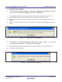
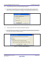
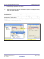
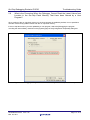
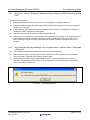
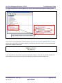
On-Chip Debugging Emulator E1/E20
2.5
Troubleshooting Guide
Why Do Values in Data Flash Memory Change Every Time I View Them in the
[Memory] Window?
The default state (immediately after erasure) of the Data Flash in RX600-series MCUs is undefined so
different values are read out every time. This is simply one of the MCU’s specifications and is not a defect.
2.6
Why Does the Message “The setting of the peripheral module clock (PCLK) is
outside the range. Please check the setting of the input clock (EXTAL) and the
system and the system clock control register (SCKCR).” Appear and Programming
Fail?
The combination of the value specified for [Input clock (EXTAL)] in the [Configuration Properties] dialog box
and the setting of the peripheral module clock selection bits in the system clock control register (SCKCR)
produces a frequency beyond the allowed range of peripheral-module clock (PCLK) frequencies.
Check both settings.
Figure 2.2
2.7
Peripheral-Module Clock (PCLK) Designation is out of Bounds
What is the Procedure When Rewriting the Flash Memory through the Program
Succeeded with the Emulator but Failed with the Actual MCU?
The data in the FCU ROM must be transferred to the FCU RAM before rewriting the flash memory in an
RX600-series MCU.
When the emulator is in use, the emulator program transfers data from the FCU ROM to the FCU RAM, so
rewriting the flash memory is possible even if the user program does not handle the transfer.
For usage of the FCU ROM and FCU RAM, refer to the user’s manual for the MCU.
R20AN0045EJ0102 Rev.1.02
Mar. 29, 2011
Page 13 of 21