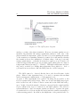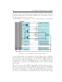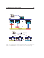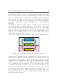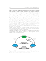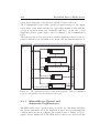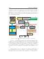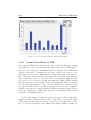
1
UNIVERSITÀ DEGLI STUDI DI BARI
Facoltà di Scienze Matematiche, Fisiche e Naturali
DOTTORATO DI RICERCA IN FISICA
XX Ciclo
Settore Scientifico Disciplinare
fis/01
The ALICE Silicon Pixel
Detector
Control and Calibration
Systems
Ivan Amos Calı̀
A.A. 2006 - 2007
UNIVERSITÀ DEGLI STUDI DI BARI
Dipartimento InterAteneo di Fisica
DOTTORATO DI RICERCA IN FISICA
XX Ciclo
Settore Scientifico Disciplinare
fis/01
The ALICE Silicon Pixel
Detector
Control and Calibration
Systems
Coordinatore: Prof. Maria Teresa Muciaccia
Supervisori: Prof. Bruno Ghidini
Dott. Vito Manzari
Dottorando: Ivan Amos Calı̀
Contents
Introduction
vii
1 The Large Hadron Collider
and the ALICE experiment
1.1 The Large Hadron Collider (LHC) . . . . . . . . . . . . . . . .
1.1.1 Machine parameters and Physics Program . . . . . . .
1.1.2 The Experiments at LHC . . . . . . . . . . . . . . . .
1.1.3 ATLAS . . . . . . . . . . . . . . . . . . . . . . . . . .
1.1.4 CMS . . . . . . . . . . . . . . . . . . . . . . . . . . . .
1.1.5 LHCb . . . . . . . . . . . . . . . . . . . . . . . . . . .
1.2 A Large Ion Collider Experiment (ALICE) . . . . . . . . . . .
1.2.1 ALICE Physics . . . . . . . . . . . . . . . . . . . . . .
1.2.2 The ALICE Detector . . . . . . . . . . . . . . . . . . .
1.2.2.1 Magnet . . . . . . . . . . . . . . . . . . . . .
1.2.2.2 Inner Tracking System (ITS) . . . . . . . . .
1.2.2.3 Time Projection Chamber (TPC) . . . . . . .
1.2.2.4 Particle Identification System (TOF, HMPID,
TRD) . . . . . . . . . . . . . . . . . . . . . .
1.2.2.5 Photon Spectrometer (PHOS) . . . . . . . . .
1.2.2.6 Electromagnetic Calorimeter (EMCAL) . . .
1.2.2.7 Forward Detectors (ZDC, PMD, FMD, FMS,
T0, V0) . . . . . . . . . . . . . . . . . . . . .
1.2.2.8 Computing and Core Software . . . . . . . . .
1.3 The ALICE Inner Tracking System (ITS) . . . . . . . . . . . .
2 The Silicon Pixel Detector (SPD)
2.1 The Detector Modules . . . . . . . . . . . . . .
2.1.1 Ladders . . . . . . . . . . . . . . . . . .
2.1.1.1 The Front-End Readout ASIC .
2.1.1.2 The Silicon Sensor . . . . . . .
2.1.2 Readout Multi Chip Module (MCM) . .
iii
.
.
.
.
.
.
.
.
.
.
.
.
.
.
.
.
.
.
.
.
.
.
.
.
.
.
.
.
.
.
.
.
.
.
.
.
.
.
.
.
1
1
1
5
6
6
7
7
7
9
11
11
11
12
13
13
13
15
16
21
24
25
25
28
29
iv
CONTENTS
2.2
2.3
2.1.3 Multi-Layer interconnect
Off-detector electronics . . . . .
Detector Services . . . . . . . .
2.3.1 Power Supply System . .
2.3.2 Cooling System . . . . .
2.3.3 Interlock System . . . .
cable
. . .
. . .
. . .
. . .
. . .
(Pixel Bus)
. . . . . . .
. . . . . . .
. . . . . . .
. . . . . . .
. . . . . . .
.
.
.
.
.
.
.
.
.
.
.
.
.
.
.
.
.
.
.
.
.
.
.
.
.
.
.
.
.
.
.
.
.
.
.
.
.
.
.
.
.
.
30
32
33
33
35
36
.
.
.
.
.
.
39
44
44
48
50
51
51
3 The SPD Detector Control System
3.1 The DCS software tools . . . . . . . . . . . . . . . . . . . .
3.1.1 PVSS and the JCOP Framework . . . . . . . . . . .
3.1.2 The State Management Interface (SMI++) language
3.1.2.1 Device Units . . . . . . . . . . . . . . . . .
3.1.2.2 Control and Logical Units . . . . . . . . . .
3.2 The SPD supervisory software layer . . . . . . . . . . . . . .
3.2.1 Front-End and Read Out Electronics Control
System (FECS) . . . . . . . . . . . . . . . . . . . . .
3.2.1.1 The FECS Local Configuration Storage . .
3.2.1.2 The FECS Driver Layer . . . . . . . . . . .
3.2.1.3 The FECS Human Interface . . . . . . . .
3.2.2 Power Supply Control System (PSCS) . . . . . . . .
3.2.3 Cooling, Interlock and Support Services
Control Systems (CCS, ICS and SCS) . . . . . . . . .
3.3 The SPD Finite State Machine (FSM) . . . . . . . . . . . .
3.3.1 FSM Top-node . . . . . . . . . . . . . . . . . . . . .
3.4 Configuration Database (CDB) . . . . . . . . . . . . . . . .
3.4.1 The FERO CDB . . . . . . . . . . . . . . . . . . . .
3.4.2 The FERO CDB Client . . . . . . . . . . . . . . . .
3.4.3 The Power Supply System CDB . . . . . . . . . . . .
.
.
.
.
.
54
56
59
60
64
.
.
.
.
.
.
.
72
75
81
83
83
87
88
4 Front-End Device (FED) Server
4.1 FED Server Internal Structure . . . . . . . . . . . . . . . .
4.2 Communication Layer . . . . . . . . . . . . . . . . . . . .
4.2.1 The Distributed Information Management (DIM)
protocol . . . . . . . . . . . . . . . . . . . . . . . .
4.2.2 FED Server - clients communication schema . . . .
4.2.3 FED Server (DIM) Commands . . . . . . . . . . .
4.2.4 FED Server (DIM) Services . . . . . . . . . . . . .
4.2.5 The Communication Layer structure . . . . . . . .
4.3 Application Layer . . . . . . . . . . . . . . . . . . . . . . .
4.3.1 ManualAccessControl and AutomaticConfFunctions
.
.
.
.
.
.
.
89
. . 90
. . 92
.
.
.
.
.
.
92
95
97
98
99
101
102
CONTENTS
4.3.2
4.4
DefaultConfiguration , ActualConfiguration
ConversionFactors . . . . . . . . . . . . .
4.3.3 DataBuffer . . . . . . . . . . . . . . . . .
4.3.4 FED Server blocks synchronization during
data acquisition and calibration . . . . . .
4.3.5 CalibrationFunctions . . . . . . . . . . . .
4.3.6 ChannelDecoder . . . . . . . . . . . . . . .
4.3.7 ExternalDataInterface . . . . . . . . . . .
Driver Layer . . . . . . . . . . . . . . . . . . . . .
4.4.1 JTAGAccess and RegistersAccess . . . . .
4.4.2 AddressGenerator . . . . . . . . . . . . . .
4.4.3 VISASessionControl . . . . . . . . . . . .
v
and
. . . . . . . 106
. . . . . . . 109
.
.
.
.
.
.
.
.
.
.
.
.
.
.
.
.
.
.
.
.
.
.
.
.
.
.
.
.
.
.
.
.
.
.
.
.
.
.
.
.
.
.
.
.
.
.
.
.
.
.
.
.
.
.
.
.
110
112
114
116
118
119
119
120
5 Detector Calibration
121
5.1 The SPD calibration specifications,
parameters and strategies . . . . . . . . . . . . . . . . . . . . 122
5.1.1 Minimum Threshold . . . . . . . . . . . . . . . . . . . 124
5.1.2 Pixel Matrix Response Uniformity . . . . . . . . . . . . 124
5.1.3 Mean Threshold . . . . . . . . . . . . . . . . . . . . . 126
5.1.4 Noise and Dead pixels identification . . . . . . . . . . . 127
5.1.5 Delay Scan . . . . . . . . . . . . . . . . . . . . . . . . 128
5.1.6 Fast-OR Efficiency and Uniformity . . . . . . . . . . . 128
5.1.7 Generic DAC Scan . . . . . . . . . . . . . . . . . . . . 129
5.2 Calibration procedures . . . . . . . . . . . . . . . . . . . . . . 129
5.2.1 DAQ ACTIVE scenario . . . . . . . . . . . . . . . . . 131
5.2.1.1 Detector Algorithms (DAs) . . . . . . . . . . 138
5.2.1.2 FXS-CDB Connector . . . . . . . . . . . . . . 142
5.2.2 DCS ONLY scenario . . . . . . . . . . . . . . . . . . . 142
5.2.3 The Reference Data Displayer (RDD) and SPD MOOD 145
5.3 Systems Applications and Detector Performances . . . . . . . 148
5.3.1 Sectors and Half-barrels Test overview . . . . . . . . . 149
5.3.2 Leakage Current . . . . . . . . . . . . . . . . . . . . . 151
5.3.3 Temperature . . . . . . . . . . . . . . . . . . . . . . . . 153
5.3.4 Minimum Threshold . . . . . . . . . . . . . . . . . . . 154
5.3.5 Noisy Pixel . . . . . . . . . . . . . . . . . . . . . . . . 155
5.3.6 Cosmic Rays Runs at DSF . . . . . . . . . . . . . . . . 156
Conclusions
159
Main Acronyms
163
vi
CONTENTS
List of Figures
166
List of Tables
172
Bibliography
173
Introduction
The work presented in this thesis was carried out in the Silicon Pixel Detector
(SPD) group of the ALICE experiment at the Large Hadron Collider (LHC).
It is hosted at the European Organization for Nuclear Research (CERN),
near Geneva (Switzerland).
The SPD is the innermost part (two cylindrical layers of silicon pixel detectors) of the ALICE Inner Tracking System (ITS). The ALICE experiment is
one of the four experiments (the others being ATLAS, CMS, LHCb), which
will operate at LHC starting by mid 2008.
In the LHC, particles (p, Pb, Ar, etc.) will be accelerated to reach energies in the TeV range and they will collide head on at very high luminosity
(1034 cm−2 s−1 for protons and 1027 cm−2 s−1 for lead ions).
During the last three years I have been strongly involved in the SPD
hardware and software development, construction and commissioning.
This thesis is focused on the design, development and commissioning of the
SPD Control and Calibration Systems. I started this project from scratch.
The work described in this manuscript is the result of my work and of a small
team of collaborators who I coordinated. After a prototyping phase now a
stable version of the control and calibration systems is operative. These
systems allowed the detector sectors and half-barrels test, integration and
commissioning as well as the SPD commissioning in the experiment.
The integration of the systems with the ALICE Experiment Control System (ECS), DAQ and Trigger system has been accomplished and the SPD
participated in the experimental December 2007 commissioning run.
This thesis is divided in five chapters. The first gives a general overview
on LHC and its expected performance. The ALICE physics and the main
features of the apparatus are described.
Chapter 2 describes the main SPD features and services. This chapter is
not intended to describe the detector in details but it only recalls the main
vii
viii
Introduction
functionality and systems structure needed for this thesis.
The actual work done as PhD activity and object of this thesis is described in chapters 3 to 5.
The complexity of the detectors, the high number of subcomponents and
the harsh working environment make necessary the development of a control system parallel to the data acquisition. This online slow control, called
Detector Control System (DCS), has the task of controlling and monitoring
all hardware and software components of the detector and of the necessary
infrastructures. The latter include the power distribution system, cooling,
interlock system, etc. As the physics experimental apparatuses grow in size
and complexity, the number of electronic channels and the sophistication
of the auxiliary systems increase proportionally. In this scenario, the DCS
assumes a key role. Its functionalities have extended well over the simple
control and monitoring of the experiment. DCS, nowadays, are highly advanced and automated online data acquisition systems, with less stringent
requirements compared to the DAQ.
Moreover the SPD DCS has the unique feature of not only controlling but
also operating the SPD front-end electronics. These requirements impose
a high level of synchronization between the system components and a fast
system response. The DCS, in this case, is a fundamental component for the
detector calibration.
The SPD DCS should be operated in the ALICE DCS framework hence a
series of integration constraint should be applied to the system.
Furthermore, in complex experiments such as ALICE, the detector operation
is tightly bound to the connection and integration of the various systems such
as DAQ, DCS, trigger system, Experiment Control System (ECS) and Offline framework. The knowledge of these systems structure and interfaces is
fundamental for the developing of the SPD DCS and calibration systems.
The operation of the SPD front-end electronics and services should be done
at various levels of integration. At the first and bottom level it is required
that each system runs safely and independently. At the second level the
subsystem controls should be merged to form a unique entity. At this stage
the components operation should be synchronized to reach the full detector operation. The third level requires the integration of the SPD control
in the general ALICE DCS/ECS. These requirements have been fulfilled by
designing the DCS with two main software layers. On the bottom a Supervisory Control And Data Acquisition (SCADA) layer controls and monitors
the equipments. It is based on a commercial application, PVSS, and it also
responsible of provide an user interface to the subsystem components.
On top a Finite State Machine (FSM) Layer performs the logical connection
Introduction
ix
between the SPD subsystems and it connects the SPD DCS with the ALICE
DCS and ECS.
PVSS is designed for slow control applications and it is not suitable for the
direct control of the fast SPD front-end electronics. I designed a Front-End
Device Server (FED Server) to interface the SCADA layer with the front-end
electronics. The server receives macro-instructions from the SCADA and it
operates autonomously the complex front-end electronics.
Chapter 3 gives a general SPD DCS overview focusing on the SCADA and
FSM layers. It describes the control of the power supplies, cooling and interlocks systems. Moreover it hosts the description of the FED Server control.
The FSM hierarchy as well as the Configuration Database (CDB) structures
is discussed.
Chapter 4 is oriented to the FED Server and it gives a general overview of
its functionality. Moreover it gives a description of the FED Server internal
structure.
Chapter 5 is dealing with the detector calibration. The detector calibration parameters are introduced and the general strategies adopted to evaluate them are described. The complexity of the detector calibration requires
a high automation level and the integration of the calibration system with
the ALICE calibration framework. In order to satisfy these requirements and
provide the user with a simple and versatile interface, I decided to foresee two
calibration scenarios. A calibration scenario, named DAQ ACTIVE, allows
the fast detector calibration but it needs the control of the full detector and
subsystems. A second calibration scenario, named DCS ONLY, slower than
the DAQ ACTIVE scenario, allows the calibration of a detector partition
without interference with the normal detector operation.
The control and calibration systems have been used to characterize and test
the SPD components before and after the integration in the detector, both
in laboratory (DSF) and in the ALICE environment. This chapter concludes
the manuscript reporting some calibration and control systems application
examples as well as a brief overview of the detector performance evaluated
during the commissioning phases.
x
Introduction
Chapter 1
The Large Hadron Collider
and the ALICE experiment
In this chapter the motivations and the main features of the Large Hadron
Collider (LHC) as well as some details of the ALICE experiment will be introduced.
In the first section the relevant accelerator parameters and the physics program allowed by the machine potential will be reviewed. The section will
focus on few aspects of the p-p physics and will give a brief overview of three
LHC experiments such as ATLAS, CMS and LHCb.
In the second section the ALICE detector and sub-detectors structures will
be described, with emphasis on the requirements imposed by the physics
program, the machine features and the technology constrains.
1.1
1.1.1
The Large Hadron Collider (LHC)
Machine parameters and Physics Program
The Standard Model (SM) predicts the existence of a yet to be seen particle,
the Higgs boson. In this theoretical model, the Higgs boson is held responsible for electroweak symmetry breaking. Many extensions of the SM, like
Supersymmetry, foresee the existence of an entire new class of undiscovered
particles. Moreover the QCD phases diagram foresees that few microseconds
after the Big Bang the matter was forming plasma of Quark and Gluons
named Quark Gluon Plasma (QGP). It was the quest for the Higgs boson,
the desire to investigate the limits of the Standard Model and its possible
extensions and the study of the QGP that brought to the construction of
the Large Hadron Collider (LHC), the most powerful particle accelerator at
1
2
The Large Hadron Collider
and the ALICE experiment
present.
Figure 1.1: The LHC machine and its injection scheme (left). Layout of the
LHC ring with the four interaction points (right).
The LHC at CERN is
√ a proton-proton and heavy ions collider with a
centre-of-mass
energy of s = 14T eV when operating in the pp mode and
√
s = 5.5T eV /A when operating in Pb-Pb mode. The accelerator is presently
under construction and is currently being installed in the LEP tunnel. The
first pp collisions at the LHC are expected to be observed in the middle of
2008. The circumference of the LEP tunnel is ∼ 27 Km and the magnetic
field needed to keep the beam circulating in the machine is provided by 1232
superconducting dipoles providing a 8.4 Tesla magnetic field. A layout of the
LHC injection and acceleration scheme is shown in Fig. 1.1. Protons will be
produced in the 50 MeV proton linear accelerator (LINAC) and they will be
injected into the 1.4 GeV Proton Synchrotron Booster. This will inject the
protons into the Proton Synchrotron (PS) accelerating them to 25 GeV and
delivering a beam of 135 bunches, containing ∼ 1011 protons. This beam is
forwarded to the Super Proton Synchrotron (SPS) which will accelerate the
protons to 450 GeV, ready to be injected into the LHC. Bunches of protons
separated by 25 ns and with a RMS length of 75 mm intersect at four points
where experiments are placed. ATLAS and CMS are general purpose experiments designed for searches for new physics and precision measurements.
LHCb is B physics and CP violation dedicated detector while ALICE is a
heavy ion experiment which will study the behavior of nuclear matter at very
high energy densities.
1.1 The Large Hadron Collider (LHC)
3
Figure 1.2: Production cross sections and event rates for various scattering
processes at hadrons colliders as a function of the machine center-of-mass
energy.
Two phases are foreseen for the LHC pp operation mode: in the first few
years of operation (low luminosity phase) the nominal luminosity is expected
to be 2 × 1033 cm−2 s−1 and then should reach 1 × 1034 cm−2 s−1 (high luminosity phase). At low luminosity approximately 10 f b−1 of data per calendar
year will be provided while one year of operation at high luminosity will
deliver 100 f b−1 of integrated luminosity. The machine will also be able to
accelerate heavy ions allowing for example Pb-Pb collisions at 1150 TeV in
the center of mass and luminosity up to 1 × 1027 cm−2 s1 .
The LHC machine will allow a broad and ambitious physics program. The
main topics are briefly summarized in the following list:
• Search for a Standard Model Higgs boson from the LEPII low mass
limit (114.6 GeV) up to the theoretical upper bound of 1 TeV. If a
Higgs boson will be discovered, its mass, width and couplings could be
measured.
4
The Large Hadron Collider
and the ALICE experiment
• Search for Supersymmetry, Extra Dimensions and other signals of physics
beyond the Standard Model up to masses ∼ 5T eV .
• Precision measurements of the SM observables such as W and top quark
masses and couplings.
• B physics and CP violation in the B hadrons system.
• Study of phase transitions from hadronic matter to plasma of deconfined quarks and gluons.
The LHC experiments will have to deal with complex working conditions
due to high centre-of-mass energy and luminosity. The total cross section
for inelastic, non-diffractive
pp interactions at the LHC is expected to be
√
around 80 mb at s = 14T eV . Fig. 1.2 shows the cross sections for different
processes as a function of the center-of-mass energy in p-p collisions.
As
√
it can be seen, the Higgs cross section increases steeply with s, while the
background remains almost constant.
At high luminosity the expected event rate is ' 109 ev/s. The physics events
can be classified as follow:
• soft collisions: they are due to long range collisions between the two
incoming protons. The final state particles from soft collisions have
large longitudinal momentum and a small transverse momentum with
< pT >' M eV . These events are also called minimum bias events and
represent by far the majority of the pp collision.
• hard collisions: they are due to short range interactions in which headon collisions take place between two partons of the incoming protons.
In these interactions the momentum transfer can be large, allowing the
production of final states with high-pT particles and the creation of
massive new particles. At the LHC the high-pT events are dominated
by QCD jet production from quarks and gluons fragmentation in the
final state which has a large cross section. Rare events with new particle production have a cross section which is usually some orders of
magnitude smaller than the jet production and therefore hadronic final
states can not be used to detect rare events such as SM Higgs boson
decay: in these conditions only decays into leptons and photons can
1.1 The Large Hadron Collider (LHC)
5
be used even if their branching ratio is much smaller than decays into
quarks.
In the pp operation mode a bunch of ∼ 1011 protons will collide at each
interaction point every 25 ns and therefore 25 soft collisions occur in average
at each bunch crossing giving rise to a total number of 1000 charged particles
in the region of |η| < 2.5. When an interesting high-pT event takes place it is
overlapped with < 25 > soft interactions which constitute the pile-up. The
detector parameters have been carefully tuned in order to reduce the impact
of the pile-up on the physics searches. The AA physics program is described
in section 1.2.1.
1.1.2
The Experiments at LHC
In total there are four experiments built to exploit LHC physics: ATLAS and
CMS are designed as general p-p experiments; LHCb will focus on B-physics
and ALICE is designed to study in details heavy ion collisions.
Figure 1.3: Schematic designs of the ATLAS, CMS, ALICE and LHCb experiments.
The Large Hadron Collider
and the ALICE experiment
6
ATLAS and CMS are two general-purpose detectors and therefore they
are designed to measure the broadest range of signals. Their main goals are
to find the Higgs boson and to look for evidence of physics beyond the standard model, such as Supersymmetry, or extra dimensions.
ALICE is optimized for studying heavy ion collisions. The temperature
and density at a collision of lead nuclei is expected to be high enough to generate a quark-gluon-plasma. In this phase quarks and gluons are almost free.
ALICE will be able to investigate heavy ion collision at an unprecedented
particle and energy density.
LHCb’s specialty is the b-physics (’B factory’). In particular it will measure the parameters of CP violation in the interactions of b-hadrons.
In the next subsections a short description of the three experiments such
as ATLAS, CMS and LHCb and their main goals is given. Section 1.2 is
devoted to the ALICE experiment.
1.1.3
ATLAS
With a length of 46 m and a diameter of 25 m ATLAS (A Toroidal LHC
ApparatuS) is the largest detector at the LHC.
The tracking detector of ATLAS consists of a Silicon Pixel Detector (SPD),
Silicon Strip Detector (SSD) and a Transition Radiation Detector (TRD). It
is surrounded by a solenoidal magnet which generates a uniform magnetic
field. The Electromagnetic Calorimeter (ECal) and the Hadronic Calorimeter (HCal) build the next two layers of the detector. They are enclosed by
the Muon Detector including the Muon Toroidal magnets. [1]
1.1.4
CMS
The main detector of CMS (Compact Muon Solenoid) is the Inner Tracker
System. It consists of 10 layers of silicon strip and pixel detector with a
total surface of ∼ 200 m2 . The next layer, the Electromagnetic calorimeter(ECAL), is built of 80000 scintillating lead tungsten crystals. The Hadronic
calorimeter (HCAL) consists of scintillators layers sandwiched with layers of
brass or steel. The HCAL is surrounded by a super-conducting solenoid
magnet which provides a 4 Tesla magnetic field. The outermost layer is the
muon system and Return Yoke. It consists of Drift Tubes (DT), Cathode
Strip Chamber (CSC) and Resistive Parallel Plate Chambers (RPC). For
high precision trajectory measurements the DTs are placed in the central
1.2 A Large Ion Collider Experiment (ALICE)
7
barrels while the CSCs are mounted in the End Caps. The RPCs are placed
in both the Barrel and the End Caps [2].
1.1.5
LHCb
LHCb is a fix target experiment using an LHC derived beam. It will look
at CP-violation using the decay modes of b-mesons. LHCb will use the
results coming from other experiments like KEK-B and PEP-II. With LHC
it will be possible to measure precisely CP-asymmetry and processes which
change the flavor of quarks and leptons. The two main detectors of LHCb are
semiconducting trackers and a Ring-Imaging-Cherenkov detector (RICH).
1.2
1.2.1
A Large Ion Collider Experiment
(ALICE)
ALICE Physics
ALICE will investigate equilibrium as well as non-equilibrium physics of
strongly interacting matter in the energy density regime ε ' 1−1000GeV /f m3 .
In addition, the aim is to gain insight into the physics of parton densities close
to phase-space saturation, and their collective dynamical evolution towards
hadronization (confinement) in a dense nuclear environment. In this way,
one also expects to gain further insight into the structure of the QCD phase
diagram (Fig. 1.4) and the properties of the Quark Gluon Plasma (QGP)
phase. In this plasma quarks and gluons do not exist in their compound
state like in hadrons but they are free inside the plasma volume. The existence and the properties of this plasma can give answers to questions of
QCD, a better understanding of the confinement and information about the
transition from the hadronic state to the QGP. Due to the inner pressure
the plasma expands and cools down until a critical temperature is reached
where the hadronization starts. The QGP will also give information about
the recreation of the chiral symmetry, the symmetry of right and left handed
particles.
At high temperature T and vanishing chemical potential µB (baryonnumber density), qualitative aspects of the transition to the QGP are controlled by the chiral symmetry of the QCD Lagrangian. This symmetry exists as an exact global symmetry only in the limit of vanishing quark masses.
Since the heavy quarks (charm, bottom, top) are too heavy to play any role
in the thermodynamics in the vicinity of the phase transition, the properties
of 3-flavour QCD are of great interest. In the massless limit, 3-flavour QCD
8
The Large Hadron Collider
and the ALICE experiment
Figure 1.4: The QCD phase diagram.
undergoes a first-order phase transition. However, in nature quarks are not
massless. In particular, the strange quark mass, which is of the order of the
phase-transition temperature, plays a decisive role in determining the nature
of the transition at vanishing chemical potential. It is still unclear whether
the transition shows discontinuities for realistic values of the up, down and,
strange quark masses, or whether it is merely a rapid crossover. Lattice calculations suggest that this crossover is rather rapid, taking place in a narrow
temperature interval around Tc ∼ 170M eV . This high temperature and density can be reached by colliding ultra-relativistic heavy nuclei i.e. lead or
gold nuclei in an accelerator like the LHC (but also at SPS energies).
The QGP cannot be observed directly due to the short life-time of this
phase. Instead other signatures have to be used to measure this medium
such as strangeness enhancement or J/Ψ suppression [3].
A series of SPS experiments were carried out using Pb projectiles of 160
GeV/A against lead (208 Pb) target. There are about 1500-2000 charged particles created in each of theses collision events and at the LHC this will go
up to 50,000. Several thousands of them are expected in the central rapidity
region, which is the region of interest for the QGP physics. The detector
system thus has to have an extreme spatial resolution to separate the particle tracks and record electronically the track (and the ionization strength) of
each traversing particle. In addition, the flight time of the particles has to be
1.2 A Large Ion Collider Experiment (ALICE)
9
measured. This allows identifying and determining momentum of all charged
particles produced in Pb-Pb head-on collision. It is also possible to identify
neutral ”strange particles” by their secondary decay into charged particles.
ALICE will have also a proton-proton program that will be an intrinsic
part of the experiment. The study of p-p collisions is essential as comparison
and reference for the study of ion-ion collisions. It will also allow comparing
results with previous experiments at SPS. It will provide first insights into
pp physics in a new energy domain, to study soft hadronic physics and its
gradual evolution for a better understanding of the perturbative QCD regime.
Furthermore, the analysis of p-p data will provide low multiplicity data to
commission and calibrate the various components of the ALICE detector [4].
1.2.2
The ALICE Detector
ALICE is a general-purpose detector designed to study the physics of strongly
interacting matter and the quark-gluon plasma in nucleus-nucleus collisions
at the LHC. The detector is designed to cope with the highest particle multiplicities anticipated for Pb-Pb reactions (dN/dy ∼8000) and it will be operational at the start-up of the LHC. In addition to heavy ions, the ALICE
Collaboration will study collisions of lower-mass ions, which are a means of
varying the energy density, and protons (both pp and p-nucleus), which provide reference data for the nucleus-nucleus collisions.
The ALICE detector (Fig. 1.5) consists of a central part, which measures
event-by-event hadrons, electrons and photons, and a forward spectrometer
to measure muons. The central part, which covers polar angles from 45o to
135o (|η| < 0.9) over the full azimuth, is embedded in the large L3 solenoidal
magnet. It consists of an Inner Tracking System (ITS) of high-resolution silicon tracking detectors; a cylindrical Time Projection Chamber (TPC); three
particle identification arrays based, respectively, on time-of-flight (TOFPID), transition radiation (TRD) and Cerenkov counters (HMPID); two
complementary electromagnetic calorimeters (PHOS, EMCAL). The forward
muon arm (2-9o , η = 2.5-4) consists of a complex arrangement of absorbers,
a large dipole magnet, and 14 planes of tracking and triggering chambers.
The set-up is completed by a set of zero-degree calorimeters (ZDCs) located
far downstream in the machine tunnel, and a forward multiplicity detector (FMD) which covers a large fraction of the phase space (|η| < 4).
The most important components of the detector are briefly discussed in the
next sections.
10
The Large Hadron Collider
and the ALICE experiment
Figure 1.5: A ALICE detector schematic draw.
1.2 A Large Ion Collider Experiment (ALICE)
1.2.2.1
11
Magnet
The optimal choice for ALICE is the L3 large solenoid with a rather weak
field (0.2 to 0.5 T) allowing full tracking and particle identification inside the
magnet. The available space has to be sufficiently large to accommodate the
PHOS, which must be placed at a distance of ∼ 5m from the vertex, because
of the large particle density.
1.2.2.2
Inner Tracking System (ITS)
The basic functions of the inner tracker - secondary vertex reconstruction
of hyperon and charm decays, particle identification and tracking of lowmomentum particles, and improvement of the momentum resolution - are
achieved with six barrels of high-resolution detectors. Because of the high
particle density, the innermost four layers need to be truly two-dimensional
devices, i.e. silicon pixel and silicon drift detectors. The outer layers at
distance r ∼ 40 cm from the beam axis will be equipped with double-sided
silicon micro-strip detectors. Four of the layers will have analogue readout for
independent particle identification via dE/dx in the non-relativistic region,
which will give the inner tracking system a stand-alone capability as a low
pT particle spectrometer. More details about the Inner Tracking System will
be presented in section 1.3.
1.2.2.3
Time Projection Chamber (TPC)
The Time Projection Chamber is the main detector in the central barrel of
ALICE. Its functions are:
• track finding with an efficiency better than 90 %;
• charged particle momentum measurement with a resolution better than
2.5% for electrons with a momentum of about 4 GeV/c;
• particle identification with a dE/dx resolution better than 10% and
• two-track separation in the region of pT < 10 GeV /c and a pseudorapidity of |η| < 0.9
The TPC is a cylindrical gas detector with an active volume between 90
cm to 250 cm in radial direction and a length of 500 cm along the beam
axis. A high voltage (HV) electrode is located at its center, which will be
aligned to the interaction point, dividing the barrel into two symmetric drift
volumes of 250 cm length. The HV electrode, which consists of an aluminized
12
The Large Hadron Collider
and the ALICE experiment
stretched Mylar foil, and two opposite axial potential degraders create a
highly uniform electrostatic field. The potential of the drift region is defined
by Mylar strips wound around 18 inner and outer support rods [5], [6]. The
design is optimized for good double-track resolution; in particular, the use of
N e/CO2 (90/10) minimizes electron diffusion and reduces the space charge.
The 72 pad-readout chambers are arranged in two end plates of 18 azimuthal
sectors at both ends of the TPC, and feature 570,000 channels.
1.2.2.4
Particle Identification System (TOF, HMPID, TRD)
A special task of the ALICE experiment is to identify the mass of the particles emitted. If the low energy particles may be identified by the loss of
energy, the higher ones are detected measuring the time it takes for a particle
to fly from the collision point to the detector barrel which is 3.5 meters away.
At even larger energies where the yield of particles is low, ALICE makes use,
for PID, of a smaller detector (14m2 ) called HMPID. This detector is based
on the detection of Cherenkov photons emitted by the particles in a dielectric medium. Hence the detector is called a RICH (Ring Imaging CHernkov)
because the pattern of the photons detected by a Cesium Iodide (CsI) photocathode is ring like. A Transition Radiation Detector (TRD) allows electron
identification above 1 GeV/c.
The Time of Flight (TOF) will allow a separation of kaons from pions up
to 2.5 GeV/c or protons from kaons up to 4 GeV/c, which requires a global
time resolution of ∼ 100 ps. The ALICE TOF is arranged in 18 supermodules, covering 360o in azimuth and a range in pseudo-rapidity of |η| < 1 with
a total area of ∼ 150m2 . Each supermodule consists of five modules, containing between 15 and 19 Multigap Resistive Plate Chambers (MRPC) strips.
Each strip contains two stacks of resistive glass plates, separated with equal
sized spacers, creating a series of uniform gas gaps with voltage applied to
the external surfaces. The MRPC stack is made of 6 glasses forming 5 gaps
with 250 µm width [7], [8].
The High Momentum Particle Identification Detectors (HMPID) consists
of seven 1.5 m × 1.5 m RICH proximity focusing counters, mounted at a
radial distance of 4.7 m from the interaction point on a space frame, covering 5 % of the ALICE barrel acceptance. Each of these modules contains six
0.64 m × 0.4 m CsI photocathodes (PCs) covering a total active area of 11 m2 .
The HMPID identifies pions and kaons in the range of 1 < pT < 3GeV/c and
protons and kaons in the range of 2 < pT < 5GeV/c. The low yield of high-
1.2 A Large Ion Collider Experiment (ALICE)
13
momentum particles in Pb − Pb collisions at the LHC energy regime justifies
the single-arm geometry of the HMPID [9], [10].
The Transition Radiation Detector (TRD) will be installed between the
space frame and the Time Projection Chamber. The TRD barrel has a radius
range between 2.9 m and 3.7 m from the beam axis and 7 m length along
the beam axis covering the central rapidity region of |η| < 0.9. The TRD is
divided into 540 modules organized in 18 sectors and 6 layers. The detector
has a total area of 750 m2 of gas chambers with radiators for particle tracking
and electron identification above 1 GeV/c. The TRD will also contribute to
the trigger system on high-pT e+ e− pairs in order to reduce the collision rate
to the readout event rate, by increasing the statistics on rare signals such
J/Ψ and Υ [11], [12].
1.2.2.5
Photon Spectrometer (PHOS)
The Photon Spectrometer is optimized to measure photons with a high resolution and to detect light neutral mesons (π 0 and η) through their twophoton decay. The PHOS has been designed to cover the pseudorapidity
range |η| = 0.12 and an azimuthal domain of 100 degrees. The detector
consists of 5 identical modules, each with 3584 channels, 17920 in total.
Each detection channel consists of a 2.2 × 2.2 × 18 cm3 lead-tungsten crystal, PbWO4 (PWO), coupled to an Avalanche Photo-Diode (APD) and a
low-noise preamplifier [13].
1.2.2.6
Electromagnetic Calorimeter (EMCAL)
The Electromagnetic Calorimeter is a large Pb-scintillator sampling calorimeter with cylindrical geometry, located ∼4.5 m radial from the beam axis inside
the L3 magnet. Covering a range in pseudo-rapidity of |η| < 0.7 the EMCAL
is positioned opposite in azimuth to the PHOS. The calorimeter is segmented
into 12672 projective towers, each covering δη × δφ ∼ 0.014 × 0.014. The
Readout fibers are coupled to an Avalanche Photodiode (APD) sensor. The
EMCAL provides level 0 and 1 triggers for photons, electrons and jets [5].
1.2.2.7
Forward Detectors (ZDC, PMD, FMD, FMS, T0, V0)
The Forward Muon Spectrometer (FMS) is designed to cover the complete
spectrum of heavy quarkonia states (c c̄, b b̄) i.e. J/Ψ, Ψ0 , Y, Y”, Y” through
their decay channels in two muons, both in proton-proton and in heavy-ion
collisions. The angular acceptance of the muon spectrometer is from 2o to
14
The Large Hadron Collider
and the ALICE experiment
9o (|η| = 2.5 − 4). Its mass resolution will be better than 100 MeV at about
10 GeV, sufficient to separate all quarkonia states. It consists of a composite absorber, made with layers of both high- and low-Z materials, starting
90 cm from the vertex, a large dipole magnet with a 3 Tm field integral
placed outside the L3 magnet, and 10 planes of thin, high-granularity tracking stations. A second absorber at the end of the spectrometer and four
more detector planes are used for muon identification and triggering. The
spectrometer is shielded throughout its length by a dense absorber tube, of
about 60 cm outer diameter, which surrounds the beam pipe.
The pre-shower Photon Multiplicity Detector (PMD) has a fine granularity and full azimuthal coverage in the pseudo-rapidity region 1.8 ≤ η ≤ 2.6.
It will be mounted on the L3 magnet door 5.8 m from the interaction point.
Charged particles are rejected using a charged particle veto (CPV) in front
of the converter. Both the CPV and the pre-shower converter are based on
a honeycomb proportional chamber design. There are ∼ 2 × 10⁵ cells each
having an area of 1 cm2 . The honeycomb wall forms a common cathode,
operated at a high negative voltage. The signal will be readout from the anode wires at ground potential using GASSIPLEX front-end electronics. The
PMD will be able to take data in conjunction with the dimuon spectrometer
and other high rate detectors [14].
The FMD consists of 51,200 silicon strip channels distributed over 5 ring
counters. There are two types of ring counters which have 20 and 40 sectors
each in azimuthal angle. The main function of the FMD is to provide precise
charged particle multiplicity measurements in the pseudorapidity range of
−3.4 ≤ η ≤ −1.7 and 1.7 ≤ η ≤ 5.0, respectively. Due to the readout time
of ≈ 13 µs the FMD will only contribute to the level 2 trigger in ALICE. Together with the pixel detector system the FMD will provide charged particle
multiplicity distributions for all collision types in the pseudorapidity range
of −3.4 ≤ η ≤ 5.0 [15].
The T0 detector consists of 2 arrays of PMTs equipped with Cherenkov
radiators and positioned on the opposite side of the IP. The main task of
the T0 is to supply a signal for the level 0 trigger for ALICE, in particular for the TRD and delivering a reference time for the TOF. The T0 has
a time resolution better than 50 ps and covers a range in pseuo-rapidity of
−3.3 ≤ η ≤ −2.9 and 4.5 ≤ η ≤ 5.0, respectively.
1.2 A Large Ion Collider Experiment (ALICE)
15
The V0 consists of 2 disks of segmented plastic scintillator tiles (8 segments) readout by optical fibers. It covers approximately the same range in
pseudo-rapidity as the FMD. The main functionality of the V0 system is to
provide the online L0 centrality trigger for ALICE by setting a threshold on
deposited energy, and to provide a background rejection capability for the
dimuon arm.
The event by event determination of the centrality plays a basic role in
heavy ion collisions. It is used at the trigger level to enhance the sample of
central collisions and to estimate the energy density reached in the interactions. The Energy ES carried away by non-interacting nucleons (spectators)
is the measurable quantity most directly related with the centrality of the
collision. The ZDC consists of two radiation hard calorimeters, one for the
spectator neutrons, the other for the spectator protons made of quartz-fiber,
which allows a very compact design of the detector [16].
1.2.2.8
Computing and Core Software
For complex systems, such as the ALICE detector (and the other CERN
detectors), an object oriented approach, implemented in C++, is now the
choice of software developers. The move to this mainstream software technology will help to manage the process of change over the long lifetime of
the experiment. C++ releases have been made of the functional prototypes
of the most important software components. The data storage, networking
and processing power needed to analyze data is in excess of those of today’s
facilities. Technological advances will help to make the data analysis possible
in a distributed environment. Several groups were started with the aim of
developing the reconstruction and selection procedures (algorithms and software) starting from the output of the Level-1 trigger, and aiming ultimately
at the full offline reconstruction.
In the original ALICE design the scope of the trigger system was very limited, essentially providing a gate to the TPC for central events and protecting
against pileup. With the increasing importance of low-cross section, highpt observables, and the successive addition of the muon arm and especially
the TRD, the demands on the trigger system have increased dramatically.
It now includes a pretrigger, three hardware trigger levels (L0, L1 and L2)
and a processor based High Level Trigger (HLT). The pretrigger, essentially
detecting an interaction using the small angle counters (T0, V0), provides
in less than 100 ns a wake-up signal to the TRD front-end, thus allowing
16
The Large Hadron Collider
and the ALICE experiment
its digital electronics to be in a low-power mode most of the time. The L0
(at 1.2 µs) and L1 (at 6.5 µs) triggers gate the fast detectors, while only
at the end of the TPC drift time (after about 100 µs), a L2 decision can
be reached, which includes an elaborate and flexible past-future protection
scheme. After the L2 decision the readout of all detectors is initiated.
The HLT implements features of online analysis of the full event during the
data readout, by using both a dedicated computer farm and distributed intelligence in the data receivers and local data concentrators. HLT functions
will include flexible trigger algorithms, data compression, and advanced online tracking possibilities.
A general framework called the ALICE Data Acquisition Test Environment
(DATE) system has been developed to operate the DAQ system. The communication between the DAQ system and the detectors electronics is performed via optical link: the ALICE Detector Data Link or DDL. In order to
collect a sufficient number of events for physics analysis in the short heavy-ion
running period (roughly one month per year), and given the large amount of
information carried for each event (up to several 10 Mbytes) the DAQ system
is designed to have a very large bandwidth of up to 1.25 Gbytes/s on mass
storage.
1.3
The ALICE Inner Tracking System (ITS)
The ITS consists of six cylindrical layers of coordinate-sensitive detectors.
It covers the central rapidity region (|η| ≤ 0.9) for vertices located within
the length of the interaction diamond (±1σ), i.e. 10.6 cm along the beam
direction (z). The detectors and front-end electronics are held by lightweight
carbon-fiber structures. Fig. 1.6 displays the ITS structure.
The number and position of the layers are optimized for efficient track finding and impact parameter resolution. In particular, the outer radius is determined by the track matching with the TPC, and the inner one is the
minimum compatible with the radius of the beam pipe (3 cm).
The silicon detectors feature the high granularity and excellent spatial precision required. Because of the high particle density, up to 90 per squared centimeter, the four innermost layers (r < 24 cm) must be truly two-dimensional
devices. For this task Silicon Pixel Detectors (SPD) and Silicon Drift Detectors (SDD) were chosen. The two innermost layers of the ITS are fundamental in determining the quality of the vertexing capability of ALICE (determination of the position of the primary vertex, measurement of the impact
parameter of secondary tracks from the weak decays of strange, charm and
beauty particles).
1.3 The ALICE Inner Tracking System (ITS)
17
Figure 1.6: General view of the Alice Inner Tracking System. It consists of
six cylindrical layers of silicon detectors.
18
The Large Hadron Collider
and the ALICE experiment
Several motivations led to the choice of equipping ALICE with a barrel of two layers of Silicon Pixel Detectors. A silicon detector with a twodimensional segmentation combines the advantages of unambiguous twodimensional readout with the characteristics of silicon microstrip detectors
such as: geometrical precision, double-hit resolution, speed, simplicity of calibration and the ease of alignment. In addition, a high segmentation leads
naturally to a low individual diode capacitance, resulting in an excellent
signal-to-noise ratio at high speed. The SPD will be described in more detail
in chapter 2.
Silicon Drift Detectors (SDD) have been selected to equip the two intermediate layers of the ITS, since they couple a very good multi-track capability
with dE/dx information.
At least three measured samples per track, and therefore at least four layers
carrying dE/dx information are needed. The SDDs, each 7.0 × 7.5 cm2 in
active area, are mounted on linear structures called ladders, each holding six
detectors for the inner and eight detectors for the outer layer. The detector
consists of two barrel layers located at radii 14.9 and 23.8 cm, respectively.
The inner layer is composed in total of 14, the outer layer of 22 ladders[17].
The two outer layers, where the track densities are below 1 per cm2 , are
equipped with Silicon Strip Detectors (SSDs). They are crucial for the connection of tracks from the ITS to the TPC. The two layers of the detector at
radii 39.1 and 43.6 cm are made of double-sided strip detectors (SSD) and
have a length of 45.1 and 50.4 cm, respectively. The sensors, each with 768
strips of 25 - 50 µm wideness and 95 µm pitch, have an area of 75 × 42 mm2
and a thickness of 300 µm. The stereo angle between the strips on one sensor is ±17.5 milliradians. The SSD also provides dE/dx information to assist
particle identification for low-momentum particles [18], [19].
Double-sided microstrips have been selected rather than single-sided ones
because they introduce less material in the active volume. In addition they
offer the possibility to correlate the pulse height readout from the two sides,
thus helping to resolve ambiguities inherent in the use of detectors with projective readout.
With the exception of the two innermost pixel planes, all the ITS layers
will have analogue readout for particle identification via a dE/dx measurement in the non-relativistic region. This will give the inner tracking system
a stand-alone capability as a low-pT particle spectrometer.
1.3 The ALICE Inner Tracking System (ITS)
19
The large number of channels in the layers of the ITS requires a large number
of connections from the front-end electronics to the detector and to the readout. The requirement for a minimum of material within the acceptance does
not allow the use of conventional copper cables near the active surfaces of the
detection system. Therefore TAB bonded aluminum multilayer micro-cables
are used.
The ITS four outer layers are assembled onto a mechanical structure made
of two end-cap cones connected by a cylinder placed between the SSD and
the SDD layers. Both the cones and the cylinder are made of lightweight
sandwiches of carbon-fiber plies and Rohacell. The carbon-fiber structure
includes also the appropriate mechanical links to the TPC and to the SPD
layers.
The latter are assembled in two half-cylinder structures, specifically designed
for safe installation around the beam pipe. The end-cap cones provide the
cabling and cooling connection of the six ITS layers with the outside services.
20
The Large Hadron Collider
and the ALICE experiment
Chapter 2
The Silicon Pixel Detector
(SPD)
This chapter gives a general overview on the Silicon Pixel Detector (SPD)
components and services. Its main goal is to introduce the SPD features
needed for the understanding of this thesis. A detailed SPD description can
be found in ALICE literature such as reported in this manuscript references.
Chapter 1 introduced the ALICE apparatus and explained the physics reasons that lead to the need of an Inner Tracking System. The introduction of
this chapter recalls the system specification whereas in section 2.1 the detector modules (Half-Staves) are described. Sections 2.2 and 2.3 are intended
to introduce the SPD off-detector electronics and services.
The Silicon Pixel Detector (SPD) constitutes the two innermost layers of
the ALICE Inner Tracking System (ITS) at radii of 3.9 cm and 7.6 cm, respectively. It is a fundamental element for the determination of the position
of the primary vertex as well as for the measurement of the impact parameter of secondary tracks originating from the weak decays of strange, charm,
and beauty particles [53]. The SPD will operate in a region where the track
density could be as high as 50 tracks/cm2 , and in relatively high radiation
levels: in the case of the inner layer, the integrated levels (10 years, standard
running scenario) of total dose and fluence are estimated to be 2.5 kGy and
3 × 10¹² n/cm2 (1 MeV neutron equivalent), respectively [61].
The SPD design implements several specific solutions to minimize the
material budget. Therefore, the materials used are as thin as possible using
wherever possible light weight materials. As a result the average material
traversed by a straight track perpendicular to the detector surface is less than
1 % X0 per layer. It is the lowest value for pixel detectors at the LHC.
21
22
The Silicon Pixel Detector (SPD)
Moreover a unique feature of the SPD is that it can provide a prompt multiplicity trigger within the latency of the L0 trigger (850ns) [20].
Figure 2.1: A schema of two adjacent sectors. On the bottom the beam-pipe
is visible. The HS numbering schema is reported.
The SPD is based on hybrid silicon pixels, consisting of a two-dimensional
matrix (sensor ladder) of reverse-biased silicon detector diodes bump-bonded
to readout chips. Each diode is connected through a conductive solder bump
to a contact on the readout chip corresponding to the input of an electronics
readout cell. The readout is binary: in each cell, a threshold is applied to the
pre-amplified and shaped signal and the digital output level changes when the
signal is above a set threshold. This technique had already been successfully
applied in the WA97 and NA57 experiments at CERN.
The ladder consists of a silicon sensor matrix bump bonded to 5 front-end
Figure 2.2: Half-barrel assembled on reference table.
The Silicon Pixel Detector (SPD)
23
chips [45]. The sensor matrix includes 256 × 160 cells measuring 50 µm (rϕ)
by 425 µm (z).
The basic detector module is the Half-Stave (HS). A HS is an assembly of
two ladders glued and wire-bonded to a high density aluminum/polyimide
multi-layer interconnect cable (Pixel Bus) that distributes power and connect
the Pixel Chips to a readout Multi Chip Module (MCM) [21].
The MCM controls the front-end electronics and is connected to the offdetector electronics readout system via optical fiber links.
Two Half-Staves are attached head-to-head along the z direction to a Carbon
Fiber Support Sector (CFSS), with the MCMs at the two ends, to form a
stave.
Figure 2.3: The SPD installed around the beryllium beam pipe.
Each sector supports six staves: two on the inner layer and four on the
outer layer (Fig. 2.1). Ten sectors are then mounted together around the
beam pipe to close the full barrel. In total, the SPD (60 staves) includes 240
ladders with 1200 chips for a total of 9.8 × 10⁶ cells.
Fig. 2.2 shows a half-barrel assembled and ready to be integrated in the pixel
mechanics. Fig. 2.3 shows the SPD installed around the beryllium beam pipe
in the experiment.
In counting room zero suppression and data encoding are performed in the
Link Receiver mezzanine cards (LinkRx card ) in the VME based Router
readout modules (Router cards )[23]. One Router card with three LinkRx
cards serves a Half-Sector (6 HSs) and has optical links to the experiment
24
The Silicon Pixel Detector (SPD)
DAQ and trigger system.
Fig. 2.4 displays the block diagram of the full SPD electronics and connections. The next sections describe in details the various elements of this
diagram.
Figure 2.4: The SPD electronics block diagram.
2.1
The Detector Modules
The basic detector module is the Half-Stave (HS) which consists of one MCM
and two sensor ladders glued on a Pixel Bus [24]. The connections between
the Pixel Bus, readout chips and the MCM are carried out via ultra-sonic
wire-bonding using 10 × 103 (32 data lines, 71 lines for control, test and
power purposes) aluminum wire bonds of 25 µm diameter. The edge of the
2.1 The Detector Modules
25
pixel bus is connected to the MCM, which controls the entire communication
from and to the off-detector electronics. A grounding foil, consisting of an
aluminum/polyimide laminate (25 µm and 50 µm thick, respectively), which
is glued between the carbon fiber and the readout chip, completes the layout
of the HS. The grounding foil provides electrical isolation with respect to the
carbon fiber support.
Two copper/polyimide laminates are connected to the Pixel Bus and the
MCM to provide power to the readout electronics and the sensors. Each
Half-Stave is supplied with 1.85 V/ 5.5 A for the Bus and 2.6 V/ 0.5 A for
the MCM, respectively [25]. Fig. 2.5 shows the HS structure (a), components
(b) and the HS cross section (c).
2.1.1
Ladders
One sensor ladder consists of 5 ALICE Pixel Chips which are flip-chip bonded
to one p-in-n sensor. The flip-chip bonding is carried out at VTT1 using PbSn bump bonds of ≈ 25 µm diameter [26]. The next sessions give more
details on the ladder components.
2.1.1.1
The Front-End Readout ASIC
The ALICE pixel readout chip is a mixed signal ASIC developed in an IBM
0.25 µm CMOS process (6 metal layers) with radiation-tolerant layout design [48]. Each chip contains 8192 readout cells of 50 µm × 425 µm arranged
in 32 columns and 256 rows. Each readout cell is connected via bump bonds
to a sensor cell.
The size of the chip is 13.5 mm × 15.8 mm including internal DACs, JTAG
controller, chip controls and wire bonding pads. The chip clock frequency is
10 MHz. A detailed description of the chip architecture can be found in [51],
[45] whereas Fig. 2.6 shows the readout pixel cell block diagram.
Each readout cell contains a preamplifier-shaper with leakage current
compensation, followed by a discriminator. A signal above threshold generates a logical 1 which is propagated through a delay line during the L1
trigger latency (∼6 µs). A four-hit-deep multi-event buffer in each cell allows derandomization of the event arrival times. Upon arrival of the L1
trigger, the logical level present at the end of the delay line is stored in the
first available of the 4 multi event buffer locations.
1
VTT Center for Microelectronics, Espoo, Finland, http://www.vtt.fi/index.jsp.
26
The Silicon Pixel Detector (SPD)
(a)
(b)
(c)
Figure 2.5: The HS structure (a), components (b) and cross section (c).
2.1 The Detector Modules
27
Figure 2.6: The readout pixel cell block diagram.
Upon arrival of the second level trigger (L2), the data contained in the
multi event buffer locations corresponding to the first (oldest) L1 trigger
are loaded onto the output shift registers. Then, for each chip, the data from
the 256 rows of cells are shifted out during 256 cycles of a 10 MHz clock.
At each cycle, a 32-bit word containing the hit pattern from one chip row is
output on the 32-bit data bus where it is processed by the MCM and sent
optically to the readout electronics located in the control room.
One pixel chip is readout in 25.6 µs. The 10 chips on each Half-Stave are
readout sequentially.
The Pixel Chip includes many operation parameters remotely adjustable.
The on-chip global registers include 42 8-bit DACs that adjust current and
voltage bias references, L1 trigger delay, global threshold voltage, and leakage
compensation. In each pixel cell a 3-bit register allows individual tuning of
the threshold; there is also provision to enable the test pulse input and to
mask the cell. All configuration parameters are controlled by the Digital
Pilot via the serial interface following the IEEE JTAG standard[27].
The chips are in daisy chain respect to the JTAG lines. Each Pixel Chip has
two JTAG circuitry input (TDI) lines for redundancy in the chain. In case of
a faulty chip the configuration data can be bypassed to the subsequent chip.
Fig. 2.7 displays JTAG connection between chips.
The Pixel Chip has proven to be insensitive to a total ionization dose (TID)
of 10 Mrad. The main specifications of the ALICE SPD front-end chip are
summarized in Tab. 2.1.
28
The Silicon Pixel Detector (SPD)
Figure 2.7: The Pixel Chips JTAG daisy chain.
Cell size
Number of cells
Minimum threshold
Threshold uniformity
L1 latency
Operating clock frequency
Radiation tolerance
Power consumption
50 µm (rϕ) × 425 µm (z)
256 (rϕ) × 32 (z)
1000 e
200 e
up to 51 µs
10 MHz
> 10 Mrad
∼ 990 mW
Table 2.1: Main specifications of the ALICE SPD front-end chip [46].
A special feature of the ALICE SPD is the Fast-OR (FO) signal. Whenever a pulse above the threshold is produced by a hit it will trigger a Fast-OR
signal. This signal is produced after the threshold discrimination and sent
to the off-detector electronics without further processing in the readout cells
allowing a fast response. The individual cells are ORed together to generate
one Fast-OR pulse for each chip. Thus, the SPD can provide 1200 independent Fast-OR signals to the L0 trigger decision (800 from the outer and 400
from the inner layer) [28].
2.1.1.2
The Silicon Sensor
The pixel sensors (Fig. 2.8) have an active size of 70.7 mm × 12.8 mm. They
are produced on 5” high resistivity n-type silicon wafers of 200 µm thickness
to comply with the material budget constraints. The sensors contain a pixel
matrix of 5 ×(32 × 256) pixel cells of 50 µm × 425 µm elongated to 625 µm
in the boundary region to assure coverage between readout chips.
2.1 The Detector Modules
29
Figure 2.8: The 5” sensor wafer. The picture shows the front side of the
sensor with large pixel sensors in the center of the wafer. Different test
structures and single chip sensors are placed around the sensor edge.
2.1.2
Readout Multi Chip Module (MCM)
A Multi Chip Module (MCM) is located at the outer end of each Half-Stave.
It houses the readout and control electronics and consists of four ASICs: the
Analog Pilot, the Digital Pilot, the GOL and the RX40. These ASICs have
been developed in the same IBM 0.25 µm CMOS process used for the Pixel
Chip. Fig. 2.9 shows an MCM picture.
The MCM is based on a 5-metal-layer sequential build-up substrate (polyimide/copper). The floorprint is 110 mm x 12 mm. Due to space constraint
the thickness is less than 1.5 mm. This has been achieved by mounting bare
die ASICs and by the development of a custom optical package2 .
The MCM data/signal lines are wired bonded to the Pixel Bus. Power is
supplied to the Pixel Bus and the MCM using two independent flexible copper/polyimide laminates (power extenders). The communication between
the MCM and the counting room is via optical links on three single-mode
fibers.
The Analog Pilot [29] chip provides reference voltages to the 10 pixel
chips and contains an ADC for monitoring the currents and voltages. Two
ADCs read also the Pt1000 temperature sensor chains on the Half-Stave.
The Digital Pilot [30] transmits the signals and configuration data to the
2
STMicroelectronics, Milan, Italy.
30
The Silicon Pixel Detector (SPD)
Figure 2.9: Multi Chip Module (MCM). Left to right: wire bonds connecting
the MCM ASICs via the Pixel Bus to the readout chips, MCM ASICs, optical
package with three optical fibers.
Router cards located in the control room and provides timing, control and
readout for the Half-Stave. The Digital Pilot receives serial trigger, configuration data and clock via the two PIN diodes in the optical package and
the receiver chip RX40. The Digital Pilot initiates the Pixel Chip readout, performs data multiplexing and sends the data to the G-link compatible
800 Mbits/s serializer GOL (Gigabit Optical Link) [31] which drives the laser
in the Optical component.
The latter is a custom designed optical transceiver housed in a silicon package
and contains two PIN diodes and one laser diode. The module is extremely
compact with a floorprint of 116 mm × 6 mm and a thickness of 1.2 mm and
has bond pads for electrical connections.
The MCM carries the reference analogue voltages with an accuracy of 10
mV and digital data streams at speeds of 800 Mbits/s without any observable
cross-talk effects. The incoming 40 Mb/s clock is recovered with a maximum
jitter of 42 ps allowing proper functionality of the 800 Mbits/s G-Link. The
jitter on the 800 Mbit/s stream is as low as 11 ps. The optical noise margin
for the incoming and outgoing data is higher than 14 and 9 dB, respectively,
and is adequate to compensate for radiation effects and ageing.
2.1.3
Multi-Layer interconnect cable (Pixel Bus)
The Pixel Bus (Fig. 2.10) is a 250 µm thick 5-metal layer sequential build-up
(SBU) substrate (aluminum/polyimide). It provides the connection between
the 10 Pixel Chips and the MCM. Two Al layer are used for the power supply
and three for the signal routing. The layers are separated by a polyimide
2.1 The Detector Modules
31
Figure 2.10: Pixel bus layers structure.
foil. Each subsequent layer is 500 µm shorter than the layer below in order
to make it accessible for wire bonds. In total approximately 1000 wire bonds
are used on each Half-Stave. The connection of the three aluminum signal
layers is carried out with micronvias. The use of aluminum in place of copper
is dictated by the low-mass requirements; it is not an industrial standard and
has required a custom development3 . The overall thickness of the Pixel Bus
is ∼280 µm. A picture of the wire bonding of ladders to the bus is shown in
Fig. 2.11.
Figure 2.11: Wire bonding of ladders to Pixel Bus .
3
CERN TS-DEM Workshop.
32
2.2
The Silicon Pixel Detector (SPD)
Off-detector electronics
The SPD off-detector readout electronics is located in the control room.
Twenty Router cards (Fig. 2.12), each carrying three 2-channel LinkRx cards,
provide the interface between the on-detector electronics and the ALICE
DAQ, Detector Control System (DCS) and trigger systems. Each LinkRx
card channel is connected to a HS. The channels consists of three optical
fiber links, one for receiving the data and two for transmission of clock, control and configuration signals.
VME Bus
connectors
DDL Module
LinkRx Cards
Optical
transceiver
Figure 2.12: SPD Router card with three LinkRx cards and a DDL module.
In the LinkRx card the pixel data stream is de-serialized, the received
data is checked for format errors and stored in a FIFO for subsequent hit
encoding. Afterward the data is zero-suppressed, encoded, reformatted and
written in the Dual Port Memory (DPM) of the LinkRx card. When all data
belonging to one event is stored in the dual memory the LinkRx card provides
an event ready flag for the Router processor. The LinkRx card confirms the
error flags that are identified in the data stream coming from the detector.
The Router card multiplexes the data incoming from the six Half-Staves into
one ALICE Detector Data Link (DDL) and it attaches trigger and status
information. The trigger information is delivered to the Router card by the
Trigger, Timing and Control (TTC) system via optical fibers.
2.3 Detector Services
33
Moreover the Router cards contributes to the temperature interlock by controlling the second Pt1000 chain. Each Router card produces an interlock
signal whenever one of the six HSs temperature passes a certain limit.
The Router cards are 9U VME and FPGA based modules having six channels
in order to connect all the optical links for the operation of one Half-Sector.
A schematic diagram of the SPD electronics system is shown in Fig. 2.13.
Figure 2.13: The readout electronics block diagram.
The 20 DDLs are connected to Local Data Concentrators (LDCs) housed
in 4 PCs. The data access from the DCS to the Router cards is established
via the router VME ports. The same port also allows monitoring and copying the data flow during data taking (data spy mode).
The 120 Half-Staves are readout in parallel. The system is able to readout
data with an average rate of ∼ 3.3KHz
2.3
Detector Services
In order to operate the SPD needs a series of support systems such as Power
Supply (PS), Cooling (CS) and Interlock (IS) Systems. The next sessions
give more details on these systems.
2.3.1
Power Supply System
The Low Voltage (LV) power supply requirements for the front-end electronics on each HS are 1.85V (∼ 6A) for the pixel bus and 2.6V (∼ 0.5A) for the
MCM. The LV Power Supply (PS) System is based on 20 CAEN4 A3009B
4
CAEN, Viareggio, Italy.
34
The Silicon Pixel Detector (SPD)
LV dc-dc converter modules (12 independent LV channels each), housed in 4
CAEN Easy3000 crates located in the ALICE cavern. The distance between
the LV PS and the detector is ∼40 m.
Each Half-Sector is powered by one LV module using the odd channels
Figure 2.14: Power supply and grounding scheme.
for the MCM and the even channels for the Pixel Bus. Remote sensing is
used throughout. In each module the Pixel Chip/MCM supply return lines
are shorted and define the Half-Stave ground. In the CAEN A3009A, all
return lines are connected via 10 kOhm resistors to a power supply reference
ground that is connected to the ALICE ground (on the absorber and the
space frame).
The detector bias voltage (High Voltage (HV) and 50V typical at start of
detector operation) is provided by CAEN A1519 modules (12 independent
HV channels each) housed in a CAEN SY1527 mainframe and located in the
control room at a distance of ∼120 m. One HV module is used for each sector. The two sensor ladders in one Half-Stave share one HV module output
2.3 Detector Services
35
but are connected by one coaxial cable each to the HV module in the control
room. This allows the individual connection of a sensor ladder to the bias
voltage. The return line of the high voltage is connected to the Half-Stave
ground via a 100 kOhm resistor. The Half-Stave ground is isolated from
the carbon fiber support using a 25 µm thick aluminum/polyimide laminate
(grounding foil). The carbon fiber support itself is connected to the ALICE
ground.
The SY1527 mainframe is the system brain and it communicates with the
software layer via ethernet (TCP/IP, OPC protocol). The DCS downloads
in the mainframe the devices configurations and the mainframe monitors and
configures the system. In case of errors such as over-current, over-voltage,
trip, etc. the mainframe switches off the corresponding channels/boards. The
SY1527 communication with the LV modules is via a CAEN A1676 branch
controller.
The Easy3000 crates are supplied by remote controllable CAEN power converter (48 V).
Fig. 2.14 illustrates the power supply and grounding scheme.
2.3.2
Cooling System
The power dissipated in the front-end electronics is ∼ 1.35 kW hence efficient
cooling is vital for this very low mass detector.
The cooling system is of the evaporative type and is based on C4 F10 . The
sectors are equipped with cooling capillaries embedded in the sector support
and running underneath the staves (one per stave). The heat transfer from
the front-end chips is assured with high thermal conductivity grease. The
SPD barrel is surrounded by an Al-coated carbon-fiber external shield to
prevent radiation of heat towards the SDD layers.
The major contribution to the on-detector power dissipation is due to frontend chips; they generate a heat load of ∼23 W (nominal) in each stave. The
design of the cooling system has been driven by various constraints such as
low material budget, long-term stability against corrosion, chemical compatibility, minimal temperature gradients, cooling duct temperature above the
dew point.
Several possible solutions based on different coolants have been considered [62]. An evaporative system with C4 F10 as coolant has been chosen
to fulfill the requirements. The C4 F10 follows a Joule-Thomson cycle (rapid
expansion at constant enthalpy and subsequent evaporation).
The liquid, overcooled and compressed by a pump, is brought to the coex-
36
The Silicon Pixel Detector (SPD)
istence phase inside the cooling duct by a pressure drop inside the capillaries
(0.5 mm internal diameter, 550 mm long). Heat abduction through phase
transition takes place inside the cooling tube at 15-18 o C (1.9-2.0 bar); a
compressor raises then the pressure pushing the gas towards a condenser,
where the liquid phase is re-established by heat transfer to cold water (∼6
o
C).
The evaporation temperature can be controlled by regulating the pressure in
the return line, setting then the coexistence conditions of the mixed phase.
Each stave is put in thermal contact with the cooling duct mounted in a
groove on the CFSS by a thermal grease layer. The cooling duct is obtained
using Phynox tubes with a wall thickness of 40 µm and an initial diameter
of 2.6 mm, squeezed down to flat profile with an overall thickness of 600
µm in the thin dimension. Each sector is equipped with cooling collectors
at the two ends, one functioning as an inlet and the other as an outlet for
the whole sector. Extensive corrosion tests have been performed on tubes,
together with the choice of surface treatment and of fitting materials. The
cooling plant provides one main cooling line for each sector.
The cooling plant is controlled by a Programmable Logic Controller (PLC).
The communication with the DCS is via ethernet (TCP/IP) using the OPC
Server-client protocol.
2.3.3
Interlock System
The detector has very low mass and high heat dissipation. In normal operation, if a sudden failure of the cooling were to occur, the Half-Staves
temperature would increase at a rate of 1 o C/s. Continuous monitoring
and a fast, reliable safety interlock on each Half-Stave are therefore mandatory. They are based on Pt1000 temperature transducers mounted on the
Pixel Bus, next to the Pixel Chips. Two daisy chains of 5 transducers each
(interleaved positions) provide redundant measurements of the average temperature. One chain is readout in the MCM that sends the resistances values
to the off-detector electronics in the counting room. The other chain is
hard-wired to the remote interlock system, based on a Programmable Logic
Controller (PLC) that is part of the detector control and safety system.
Temperature values and trends are logged. If the temperature reaches a preset threshold (40 o C), the low-voltage power supply is promptly switched off
by the safety interlock and an alarm is generated.
The PLC scans the 120 chains in less than 1s and communicates with the
software layer via ethernet and using OPC Server-Client Protocol. All the
temperature readouts are also sent online to the counting room.
The cooling plant provides 11 interlock lines informing on the general status
2.3 Detector Services
37
T interlock Routers
(120 Pt1000 chains)
Cooling loops status
20
10
(Sectors)
20
T Interlock PLC
(120 Pt1000 chains)
LV Modules
(Half Sector
granularity)
1
Cooling plant
(General Alarm)
Software interlocks
•Sensors leakage currents
trends
•Temperature trends
(Routers & Interlock PLC)
Figure 2.15: A block diagram of the SPD interlock schema.
of the plant and on the activation status of the cooling lines. Whenever either
the plant is not running or the lines are not opened an interlock is issued.
Moreover the system foresees also two level of software interlock based on
currents and temperatures trending such as described in section 3.2.2.
The block diagram of Fig. 2.15 displays the SPD interlock schema.
38
The Silicon Pixel Detector (SPD)
Chapter 3
The SPD Detector Control
System
The SPD Detector Control Systems (DCS) is complex software application
designed to operate and monitor the SPD. The primary function of the DCS
is the overall control of the detector status. It takes appropriate corrective
actions to maintain the detector stability and ensure high quality data. It
provides an adequate user interfaces for experts or simple shifters. In addition, it communicates with external systems such as the databases and the
control systems of the accelerator.
Another main task of the DCS is the control and monitoring of the systems
environment at and in proximity of the experiment. These tasks are historically referred to as ”slow controls” and include: handling the electricity
supply to the detector, control of the cooling facilities, environmental parameters, crates and racks. Also safety related functions such as detector
interlock are foreseen by the DCS in collaboration with the Detector Safety
System (DSS). Many functions of the DCS are needed at all time. Thus the
technologies and solutions adopted must ensure a 24-hour functioning for the
entire life of the experiment.
Moreover the SPD DCS should be integrated in the general ALICE DCS and
Experiment Control System (ECS) in order to operate the SPD as an ALICE
subsystem.
The SPD DCS has also the unique feature of not only controlling but also
operate the SPD front-end electronics. These requirements impose a high
level of synchronization between the system components and a fast system
response. The DCS in this case is also a fundamental component for the
detector calibration. These needs strongly influence the system design as
described in the next sections.
The SPD DCS needs to configure roughly 20 M parameters, calibrate the
39
40
The SPD Detector Control System
∼ 50 k front-end electronics DACs and monitor ∼ 5000 variables. Moreover
the detector performance are evaluated by means of ∼ 10000 calibration parameters. The huge amount of elements to be controlled imposes high system
automation and an intuitive user interface. System performances are critical
issues in the system design.
The ALICE DCS needs to fulfill a series of requirements in order to
operate the full experiment built up of 18 sub-detectors and the experiment
services. The requirements can be summarizes as:
Partitionability: The ability to partition the DCS system is essential for
a detector like ALICE, which has a large number of sub-detector elements. Partitioning implies that a specific sub-element can be cut off
from the rest of the system and operated independently. This operation
mode is useful for maintenance and calibration.
Modularity: Modularity is achieved through a hierarchical structure of the
DCS.
Homogeneity: This characteristic will facilitate integration, maintenance,
and upgrading. The usage of commercial hardware and software follows
this guideline.
Scalability: An important uncertainty for the DCS is the exact size of the
system to be installed for the first physics run, as well as the evolution of the accelerator and experiment performance. Scalability makes
the system flexible enough to facilitate the introduction of select new
technologies in its various parts.
Automation: Automation features speed up the execution of commonly
performed actions and avoid human mistakes typical in repetitive routines.
Radiation tolerance The DCS hardware components placed in proximity
of the detector will suffer high radiation levels. Therefore, radiation
tolerant components are mandatory and sensitive equipment should be
placed as far as possible from the interaction point.
Each ALICE sub-detector should follow these guidelines for the specific
DCS implementation. Moreover, besides these general requirements, each
sub-detector has some specific ones resulting from its unique design and implementation.
The SPD Detector Control System
41
In order to fulfill the mentioned system requirements, the ALICE DCS has a
hierarchical two software layers structure as displayed in Fig. 3.1. The bottom
DCS
FSM
Det. 1
Det. 2
Det. N
…
SCADA
Worker
Node
Worker
Node
Worker
WorkerNode
Node
PVSS
PVSS
PVSS
PVSS
Worker
Node
Worker
Node
Worker
WorkerNode
Node
PVSS
PVSS
PVSS
PVSS
Worker
Node
Worker
Node
Worker
WorkerNode
Node
PVSS
PVSS
PVSS
PVSS
Hardware
DETECTORS
Figure 3.1: The DCS software layers. On top the FSM controlling logically
the devices monitored and controlled by the SCADA applications.
software layer is a supervisory layer (SCADA layer) devoted to control and to
operate the detector subsystems individually. It is responsible for stable and
safe operation of the equipments and it also provides low level user interfaces.
The operators can access directly the equipments using these interfaces. The
supervisory layer is based on a Supervisory Control And Data Acquisition
(SCADA) application and CERN standardized PVSS (see section 3.1.1 for
more details) as SCADA for all the LHC experiments. PVSS is an industrial
SCADA product from the Austrian company ETM and the acronym PVSS
is the German abbreviation for ”Process visualization and control system”.
It is a SCADA system designed specifically for the operation and supervision
of technical installations and industrial processes. Nevertheless some of its
features, described in the next sections, make it interesting for high energy
physics applications.
The upper DCS software layer hosts a Finite State Machine (FSM) performing the logical control of the full system. The FSM merges the subsystems
control to form a unique entity. It is also responsible of the systems syn-
42
The SPD Detector Control System
chronization and high level DCS automation. All the ALICE detectors have
their own FSM however the FSM top level, named top-node, is common to
all the detectors. This is a common interface used to integrate the detectors
control with the global ALICE DCS/ECS. The FSM is implemented using
the State Management Interface (SMI++)[75] (more details in section 3.1.2).
The PVSS layer (also called SCADA layer in this thesis) receives commands from the FSM and communicates with the detector hardware. Moreover PVSS hosts a FSM GUI.
All the ALICE detectors should provide the ALICE DCS with an FSM and
a SCADA (PVSS) layer. Furthermore the SPD DCS hosts a third software
layer, named Front-End Device Servers layer, connecting the SCADA layer
with the SPD front-end electronics. This layer will be widely described in
section 3.2.1 and chapter 4.
The configurations parameters needed by the DCS and by the detector hardware components are stored into a specific Configuration Database (CDB).
It is introduced in section 3.4.
In order to support the intensive computing load required by the control
system, the DCS software is scattered on a series of PCs. Each of them
runs PVSS projects, FSM elements and control support applications (e.g.
10 PCs are used by the SPD DCS). The communication between the software elements and the PCs is via ethernet. The DCS PCs are divided in
two families: Worker Nodes (WNs) and Operator Nodes (ONs). The WNs
monitor and control the hardware/software components supporting the DCS
computing load. The ONs host the system user interface and they are used
by the operator to access and operate the system. The system can be operated at various levels such as full DCS level or detector level. Each detector
has its own Operator Node and Fig. 3.2 (a) displays a typical detector DCS
structure. Fig. 3.2 (b) show the operator access at the ALICE DCS level.
The control system is designed to operate automatically in stand-alone
and to inform the operator only when an error condition is verified. However, the operator can monitor and manually operate the system logging to
specific ONs. Fig. 3.3 shows the flux of information generated by the operator accessing a hardware component using an ON and the FSM. The ONs
have a PVSS interface displaying the FSM communicating with the various
subsystems. The FSM forwards the operator commands to the appropriate
PVSS system that applies the required actions on the hardware components.
The SPD Detector Control System
43
operator
Operator Node
ON
PVSS
D
Ethernet
Worker Node
D
PVSS
Worker Node
D
PVSS
HV OPC
LV OPC
CANbus
HV Devices
worker node
worker node
Worker
PVSS Node
PVSS
D
PVSS
DIM
DIM
DIM
Ethernet
Ethernet
LV Devices
DETECTOR
FEE Devices
(a)
operator
ON
TPC
SPD
A LICE D CS
O perator N ode
TOF
(b)
Figure 3.2: A typical detector DCS structure (a). The control schema used
by the global ALICE DCS to access the detectors control systems (b).
44
The SPD Detector Control System
FSM plane
SPD
SE C0
FEE
PW
CH
CH
CH
CH
operator
SE CN
CH
CH
CH
FEE
PW
CH
CH
CH
RCU
RCU
CH
SCADA plane
commands
status, alarms
PVSS
D
D
D
PVSS
HV OPC
HV Devices
D
PVSS
D
PVSS
DIM PVSS
DIM
DIM
D
PVSS
LV OPC
LV Devices
FEE Devices
Figure 3.3: The information flux generate by an operator accessing a hardware component via ON. In this example the operator sends commands to a
HV channel using the FSM visible in the operator node. The FSM address
the corresponding driver in the various PVSS systems.
3.1
The DCS software tools
The Detector Control System has been developed using PVSS for the SCADA
layer and the State Management Interface (SMI++) for the FSM layer. This
section1 reports the main features of these two developing tools in order to
understand the structures and conventions used in this thesis. Moreover in
section 3.1.2 FSM implementation strategies are discussed.
3.1.1
PVSS and the JCOP Framework
PVSS is a Supervisory Control And Data Acquisition application designed
by ETM of the Siemens group[66]. SCADAs are commercial software systems used extensively in industry for the supervision and control of industrial
processes. SCADA systems are used in a wide variety of industrial domains
and therefore typically provide a flexible, distributed and open architecture
to allow customization to a particular application area. In addition to a set
of basic SCADA functionalities, these systems also provide a set of standard
interfaces to both hardware and software as well as an Application Program1
The DCS experts already aware of the PVSS, FSM and SMI++ functionality and
implementations, can skip this section without loosing the thesis flow.
3.1 The DCS software tools
45
ming Interface (API) to enable integration with other applications or software
systems.
PVSS is used to connect to hardware (or software) devices, acquire the data
they produce and use it for their supervision, i.e. to monitor their behavior and to initialize, configure and operate them. A wide documentation on
SCADA applications and PVSS can be found at [106] and [36] whereas in
this section only the information needed for the understanding of this thesis
are reported.
PVSS has a highly distributed architecture and a PVSS application is
composed of several software processes called Managers. A PVSS system
(named also PVSS project) is an application containing one Event Manager,
one Data Manager and any number of other Managers. An example of a
PVSS system is shown in Fig. 3.4.
Figure 3.4: An example of PVSS system in which the main manager types
are reported.
The Event Manager (EV) is the PVSS central processing unit. This unit
holds the current image of all process variables in the memory. Every other
Manager, which want to access the data, receives these data from the process image of the Event Manager and do not have to communicate directly
with a controller. Viceversa a command from a control station is set as a
value change in the process image of the Event Manager in the first instance.
Afterwards the responsible driver forwards the value to the specific target
46
The SPD Detector Control System
device automatically. The EV is a central data distributor, the communication center for PVSS. Additionally this manager executes also the alert
handling and it is in a position to make different calculation functions automatically. Managers subscribe to data and they are only sent by the Event
Manager, on change. Indeed data processing and communication between
the individual Managers is normally performed purely on an event-oriented
basis. Conversely, in steady-state operation with no changes in values, there
is neither communications nor processing load.
The Data Manager (DB) constitutes the link to the PVSS internal database.
It handles the parametrization data of an application to be saved in such a
database and the archiving of value changes and alerts.
The Drivers (D) are special programs providing the connection between
PVSS and hardware or software devices to be supervised. They convert a
specific protocol into the form of communications used internally by PVSS.
The driver can be e.g. Profibus, OPC, CanBus, Modbus, DIM, etc.
The User Interface (UI) Managers form the interface with the user. These
include a graphical editor (GEDI), a database editor (Graphical Parametrization, PARA) and the general user interface of the application (Native Vision,
UI). The PARA allows the users to define the structure of the database, define which data should be archived and define which data coming from a
device should generate alarms.
In the User Interface, values are displayed, commands issues or alerts tracked
in the list of alerts. In PVSS, the user interaction software runs completely
separately from the processing executing in the background. It merely provides a window on the live data from the process image or the archived data
in the history.
The Control Managers (CTRLs) run background scripts for any data
processing. The scripting language has largely the same syntax as ANSI-C
with extensions. It is an advanced procedural higher-level language that uses
multithreading. The code is processed interpretively so does not need compiling. Any user functions that are repeatedly needed can be stored in PVSS
libraries for use by panels and scripts.
The API Managers (API) allow the users to write their own programs in
C++ using a PVSS Application Programming Interface (API) to access the
data in the PVSS database.
3.1 The DCS software tools
47
Several instances of a manager for all manager types (UI, CTRL, D, API,
etc.) can be added to a PVSS system. Thus a number of user interfaces or
drivers can be run from one Event Manager for example. These Managers
communicate via a PVSS-specific protocol over TCP/IP and this means that
a PVSS system can be distributed across a number of computers.
PVSS allows interconnecting a number of autonomous systems into an overall
system. As shown in Fig. 3.5 a Distributed System is built by adding a
Distribution Manager (Dist) to each system and connecting them together.
Figure 3.5: An example of Distributed System.
PVSS allows users to design their own user interfaces (panels), in a ”drag
and drop” fashion. By using the Graphic Editor, the user can first design
the static part of a panel, by placing widgets like buttons, tables, plots, etc.
Actions can then be attached to each widget. Depending on the widget type,
actions can be triggered on initialization, user click or double click, text input, etc. Moreover PVSS provides the possibility to create a single symbol
or panel and to use it many times. This is called a Reference Panel. Changes
to this Reference Panel are inherited by all instances of the panel.
The device data in the PVSS database is structured as Data Points (DPs)
of a pre-defined Data Point Type (DPT). PVSS allows devices to be modelled using these DPTs. A DPT (DPTs are similar to structures in OO
terminology) describes the data structure of the device and a DP contains
the information related to a particular instance of such a device (DPs are
48
The SPD Detector Control System
similar to objects instantiated from structure in OO terminology). The DPT
structure is user definable and can be as complex as one requires and may
also be hierarchical. The elements forming a DPT are called Data Point
Elements (DPEs) and are user-definable. After defining the data point type,
the user can then create data points of that type which will hold the data
of each particular device. The creation and modification of DPTs and DPs
can be done either using the Graphical Parametrization tool (PARA), or
programmatically using ctrl scripts.
The use of PVSS has been standardized at CERN and given the evident
similarity in technical requirements for controls amongst the experiments, the
Joint Controls Project (JCOP) [107] was created. This project provides the
PVSS users with guidelines and PVSS components, which can be devices or
tools commonly used for the experiment controls. The series of components
produced by this project are called JCOP Framework components. The SPD
DCS uses some of the Framework components. In this thesis will be noticed
the uses of these elements in the various sessions.
3.1.2
The State Management Interface (SMI++)
language
The SPD control has a complex structure and this characteristic impose a
high rate of automation to control processes, to reduce human errors and
to optimize recovery procedures. Automation comes with the need to describe the behavior and evolution of the system in the most accurate way.
A solution is to view all system sub-elements (either abstract or physical) as
controllable objects whose behavior is defined through finite state automaton. A finite state automaton, or more simply a Finite State Machine (FSM),
is a model of behavior for any complex or simple object with a finite number
of states, transitions and actions. A state stores information about the past,
i.e. it reflects the input changes from the system start to the present moment. A transition indicates a state change and is described by a condition
must be met to enable the transition. An action, instead, is a description of
an activity that is to be performed at a given moment. The action may be
executed when entering the state, exiting it or during the transition.
State Management Interface (SMI++)[75] is a custom CERN language CERN
oriented to control systems FSM. CERN standardized the use of SMI++ for
all the LHC experiments.
The language is object oriented and it allows 3 basic object types: Device
Units (DUs), Logical Units (LUs) and Control Units (CUs) described in the
3.1 The DCS software tools
49
next sections. These FSM objects can be connected together to form hierarchies. The data flow is only being vertical: commands (actions) flowing
downwards, states and alarms going upwards. A command may trigger state
changes at lower hierarchy level that in return may cause state changes at
higher hierarchy ones. Fig. 3.6 displays an example of FSM hierarchy.
In the FSM hierarchy various levels are foreseen and the connections between
the objects define the roles. The objects at the same level are named children
of the object at the higher level named parent. The higher hierarchy level is
named top-node.
Figure 3.6: An example of FSM hierarchy.
An important advantage of having a hierarchical structure is the possibility to partition the command hierarchy, essential for a detector like the
SPD. Partitioning implies that a branch of the main tree is cut off. In this
way components can be operated independently from the rest of the tree: the
corresponding partition operate independently from the rest of the system.
This mode of operation will be used mainly for maintenance, calibration,
system testing and trouble shooting. The partitioning modes available are
the following: Included, Excluded, Manual, and Ignored. The meaning of
each is clearly illustrated in Fig. 3.7.
PVSS hosts a FSM toolkit provided by the JCOP Framework and based
50
The SPD Detector Control System
Figure 3.7: An example of FSM hierarchy.
on SMI++. A friendly user interface allows defining the FSM structure for
every node. It is possible to specify the states, the accepted commands, the
allowed transitions between states and the eventual actions to undertake.
Moreover the Device Units can host PVSS scripts.
3.1.2.1
Device Units
The specific tasks of a Device Unit (DU) are to interface to the actual hardware device, implement the actions to be taken on the device and retrieve
the devices state. In addition it must be able to generate alarms.
The DUs are the bottom layer objects in the FSM hierarchy indeed they
cannot have children. They are communicating with the hardware devices
via PVSS datapoints (DPs) and producing a state as function of the DPs
values retrieved. The state is re-calculated each time the DPs are updated
and the DUs are not allowed to modify autonomously their states. This
characteristic is fundamental for a device control system.
Inside the DUs is possible to use PVSS functions and run PVSS scripts. This
functionality gives strength to these objects allowing also complex sate calculation operations from a series of DPs. The DUs are the only FSM object
capable of manage operation timeout.
The DUs accept user defined commands in strings format. These commands
can be translated inside the DU to a series of operation to apply on PVSS
DPs. The list of commands is unique for all the states and the user can decide
their visibility in the different states. The DUs cannot run in stand-alone,
3.2 The SPD supervisory software layer
51
they need to be inserted in a hierarchy in which a CU is present in the higher
levels.
3.1.2.2
Control and Logical Units
The Control Units and Logical Units are pure logical FSM objects able to
configure, monitor and control its children, recover errors, handle alarms.
The difference between these object resides in the partitioning capability.
The CUs form domains containing all the elements below in the hierarchy.
They can run autonomously on a PC allowing the hierarchy scattering on various PCs. However CUs are high memory consuming (∼ 7M b each) objects.
This limitation strongly influences the hierarchy design and performances,
indeed, a CU should be used only when the system partitioning is strongly
needed. LUs can be used instead when this requirement is not stringent.
The LUs and CUs actions are state dependent and they can set parameters,
send commands to the children and change their own state.
LUs and CUs contain a list of user defined condition dependent on the children state. Whenever a child change its state, this list is checked and these
objects can either call a state action or change their state.
3.2
The SPD supervisory software layer
The SPD SCADA layer should provide monitoring of the detector conditions,
of front-end electronics, and all SPD subsystems (high voltage, low voltage,
cooling system and interlock system). All monitored data should be recorded
and archived in a common ALICE database. Furthermore the DCS should
provide early warnings in case of abnormal conditions, issue alarms and execute automatic control actions to protect the detector.
The main challenges for this layer are the large number of channels (10 M)
and parameters (more than 5000 among temperatures, voltages, currents
electronics configurations, cooling pressures, etc.) to monitor, the large data
volume, and the necessity to run the DCS during the whole ALICE detector
lifetime.
My contribution to the SPD SCADA layer was the conceptual system design
and the architectural layer structure. Moreover I coordinated the system
design activity.
The main concept in designing the DCS SCADA layer is the modularity
and the autonomous and self-consistency operation of the various subsys-
52
The SPD Detector Control System
tems. Each component should operate safely independently. The exchange
of information between subsystems must be performed only trough a specific interface. Hence every module should be able to accept requests by the
others and publish its results without allowing the changes of its parameters by other subsystems. Moreover the SCADA systems design is Object
Oriented (OO) in which every subsystem and component is seen as a selfconsistent element.
Innovative design patterns have been applied to optimize system performances, scalability and maintenance. For example each subsystems (cooling, power supply, FE electronics, etc.) control part is divided in three main
blocks such as hardware interface, user interface and automatic control to
archive these goals. This separation allows the decoupling of the three blocks
that can have an autonomous, robust, light and easy to upgrade structure.
The global system performance are strongly enhanced in term of stability,
speed and equipments operation safety. The actual details of the implementations are reported in the corresponding subsystems sections.
In order to understand the structure given to the control system is important to bear in mind that commands and status should be completely
independent. In control systems indeed a command to the hardware can
bring the system in a state completely different from the expected. This
effect can be produced as consequence of the command issued or function of
unexpected factors. Hence the control system should have two separate architectures: the command to the hardware and the status information. The
two should communicate only when automatic actions should be taken.
The SPD SCADA layer can be logically separated in four main subsystems
as displayed in Fig. 3.8. This block diagram shows the connection between
the hardware and the software components. For schematize the full DCS,
the four subsystems CSs are represented as separated elements but actually
they are strongly interacting. The Service Control (SCS) is not displayed in
the block diagram but it is responsible of establishing the link between the
various subsystems. Moreover it manages the services needed to operate the
various CSs.
The Power Supplies Control (PSCS) communicate with the CAEN mainframe managing the 360 detector power channels.
The Front-End and Read Out electronics (FERO) Control (FECS), using
two FED Server (see chapter 4 for more details), controls the off-detector
electronics and on-detector electronics. Moreover the FECS is not only a
control system but it also embeds the detector calibrations functionalities
(see chapter 5 for more details).
3.2 The SPD supervisory software layer
53
Op t ica l
Et he r n e t
VM E
Ge ne r ic
SCADA
Pow e r S uppli e s
Cont r ol ( PSCS)
- PVSS -
Hardware
1 x CAEN Mainframe SY1527
(1 x A1676 Branch Controller &
10 x A1519B 12 ch. HV Modules)
4 x CAEN Easy3000 crates
(tot. 20 x A3009B 12 ch. LV
Modules)
FERO Cont r ol
( FECS)
- PVSS -
I nt e r lo ck
Cont r ol ( I CS)
- PVSS -
Coolin g
Cont r ol ( CCS)
- PVSS -
2 x F ED S e r ve r s
- C+ + -
1 x Coolin g PLC
20 x SPD Routers
(3 x LinkRxs each)
1 x I nt e r lo ck &
Te m pe r a t ur e M onit or in g
PLC
1 x Coolin g Pla nt
( 1 0 coolin g l in e s)
1 0 x He a t e r s
Figure 3.8: A logical block diagram displaying the SPD control system
branches. In white are displayed the software components whereas in yellow
the hardware components.
The Interlock Control (ICS) manages the SPD interlock system and it
monitors the detector temperature. The parameters readout via the ICS are
widely used also by the other CSs.
The Cooling Control (CCS) operates the cooling system and a series of
heaters used to compensate the variation of heating produced by various
detector powering configurations.
In the future it is also planned to integrate the control of the Pixel Trigger (PIT) electronics in the SPD DCS.
Each CS contains translator scripts capable of converting macro-instructions
into the sequence of operations required for the hardware. Background scripts
monitor continuously the status of the hardware and take automatic actions
to protect the system in case of abnormal states. Most processes are fully
automated in order to obtain the required reliability and safety of operation.
54
The SPD Detector Control System
3.2.1
Front-End and Read Out Electronics Control
System (FECS)
The FECS is the software used to control and operate the Front-End and
Read Out Electronics (FERO) such as Router cards, LinkRx cards and HSs.
It should monitor the actual electronics status of the off-detector electronics and on-detector electronics. Moreover the FECS configure the detector
(∼ 50 k Pixel Chips DACs and 10 M pixels matrices in term of TP and
pixel masking), the Router cards and the LinkRx cards (∼ 1600 registers).
The FECS monitors the detector temperature and it performs the detector
calibration procedure.
The FECS is built up of two software layers (Fig. 3.9). On top the PVSS layer
communicating via TCP/IP with the bottom Front-End Device Server (FED
Server) layer. In this section the PVSS layer is described whereas chapter
SCADA Layer – FECS -
1 x F ED S e r ve r
- C+ + -
10 x SPD Routers
(3 x LinkRxs each)
FERO Cont r ol
( FECS)
- PVSS -
FED Servers Layer
Op t ica l
Et he r n e t
VM E
Ge ne r ic
1 x F ED S e r ve r
- C+ + -
10 x SPD Routers
(3 x LinkRxs each)
Hardware Layer
Figure 3.9: A block diagram displaying the connection between the FECSPVSS, FECS-FED Servers layer and the hardware layer.
4 is dedicated to the FED Server. In order to understand this section it is
only important to bear in mind that the PVSS is not designed for high speed
control applications and it would not suit with the complex SPD electronics
control. Hence the FED Servers receive macro-instructions from the PVSS
layer and they publish the actual detector status and configuration.
For convenience, in this chapter, FECS means FECS-PVSS layer.
The FECS is designed to operate the FED Servers in automatic and
manual mode. It provides the human interface to the detector configura-
3.2 The SPD supervisory software layer
55
tion parameters and to the detector calibration functions. Hence the system
has been designed Object Oriented and with high modularity. This design
pattern is fundamental for an application such FECS requiring data managements and often updates. The main concept in designing the FECS is
to provide the users with a common interface to the detector configuration
and calibrations passing trough either the FED Servers or the Configuration
Database.
The FECS is composed of three main blocks such as Local Configuration
Storage, Driver Layer and Human Interface. These blocks operate asynchronously and they run in specific and separated control loops. The communication between the various elements is performed only through dedicated
interfaces and the data exchange uses the Local Configuration Storage as
main gateway. The FECS structure separates the information fluxes in two
main blocks as displayed in Fig. 3.10.
The top block foresees the communication between the Human Interface
Human Interface
Local Configuration
Storage
Driver Layer
Figure 3.10: A simplified FECS PVSS layer block diagram.
and the Local Configuration Storage elements whereas the bottom block establishes the communication between the Driver Layer and the Local Configuration Storage. This structure makes the system very robust and it strongly
simplify the system maintenance. Moreover the Human Interface designers
and users are not obliged to know the full system structure but only the
Local Configuration Storage structure. Viceversa the Driver Layer needs to
communicate with only one block to store and retrieve information. The
information centralizing into the Local Configuration Storage allows expanding easily the control system adding control loops plugged directly to the
Local Configuration Storage. This design pattern also optimize system performances because all the control processes can run in separate PVSS managers, hence easily managed.
56
The SPD Detector Control System
Fig. 3.11 displays a simplified FECS collaboration diagram. In the next
sections the three main blocks will be described.
3.2.1.1
The FECS Local Configuration Storage
The Local Configuration Storage is the FECS core in which the information on the hardware status and configuration is stored. The FECS uses
the FERO DPs as information collectors and main gateway to the different
applications. Hence the FERO DPs are mapping the hardware configuration parameters such as electronics registers, DACs and noisy pixel maps.
Moreover each DP store information on the electronics status such as temperature, activation status, TPs activation, dead pixels, etc. The FERO
DPs are: 120 DPs of type HS, 60 DPs of type LinkRx card, 20 DPs of type
Router card and a series of support DPs defining the calibration parameters
to be used. All the FERO DPs have three main parts: Settings, Actual and
DefaultConfig (same structure of the FED Server storage classes described
in section 4.3.2). The Settings elements specify which configuration should
be downloaded into the electronics whereas the Actual elements store the actual electronics configuration. The DefaultConfig memorize the information
either retrieved from the Configuration Db (CDB) or to store in the CDB.
In Fig. 3.12 is displayed the Half-Stave DP type as FERO DP example. The
Analog Pilot (API) Actual and Settings DP elements have been expanded .
The Local Configuration Storage block hosts also a DataDistributor script
used to forward data to other systems. For example the detector temperatures readout via FECS and used by the PSCS to switch off hot channels.
The DataDistributor runs on a dedicated PVSS control manager reading
cyclically the FERO DPs. When a DP changes, the script forwards the data
to the appropriate system.
The StatusScripts are a series of scripts running on independent PVSS
control managers and checking online the electronics and control system status. These scripts read cyclically the information stored in the FERO DPs
Actual and Status parts and they asserts alarms, e.g. the FED Server alive
status, when an error condition is found. If one of the FED Servers either
stops operating or the communication is closed, the FED Server hearth bit
DP stops to be updated. In this case the StatusScripts generate a message
on the PVSS log and it inform the FECS thought specific FECS status DPs.
)
b(
eD
t
da
Up
Ge
tCo
n
f
i
g
ura
ti on
s( )
FECS CDB Interface
Driver Layer
StatusScripts
)
nt
()
ta me
a
e
l
tD ( e
Ge or s
r
r
tE
Se
DataDistributor
)
ta (
tDa
e
G
FERO DP
CommunicationAgents
SetReadOutData(Data)
Local Configuration Storage
Co
m
Se man
r vi
c e ds
s
DIM Clients
SendCommand(Command, Data)
Se Ge
tC tCo
on n
fig fig u
ur ra
at tio
io n
n( s
Da ()
ta
)
GetData(Element)
PVSS Panels
Human Interface
Logger
ControlLibraries
SendCommandToFed(Command)
RetrieveDataFromDb()
StoreDataToDb()
AccessDP(Data)
FECS PVSS layer
3.2 The SPD supervisory software layer
57
Figure 3.11: A simplified FECS PVSS layer collaboration diagram.
58
The SPD Detector Control System
DefaultConfig stores the configuration
information read back from the
Configuration Database
General
Status
DPEs storing information on the HS general
status such as Temperature , R- T conversion,
Configuration and Activation Status
The Analog Pilot Actual configuration
and status. These DPEs store the API
read back parameters
MCM
The Analog Pilot Setting parameters.
These DPEs store the API parameters
to be used during the API
configuration process.
PixelChips
Figure 3.12: An example of FERO DP displayed using the PVSS PARA. The
DPs of type HS (spdHalfStave) store information on the HS configuration
and status. In correspondence of the + the menu can be expanded and the
DP elements become visible. This example shows the Analog Pilot (API)
Actual, the API Settings and the hwStatus elements.
3.2 The SPD supervisory software layer
59
Sensitive FERO DPs such as detector temperature, voltages and currents
monitored by the FED Servers, are archived, on change, on an ALICE DCS
centralized archival Oracle Database. The connection to the Db is performed
running a specific PVSS manager.
3.2.1.2
The FECS Driver Layer
The FECS Driver Layer establishes the FECS communication with the FED
Servers and the Configuration Database. Two type of clients such as DIM
Client and FECS CDB Interface are managed by the Communication Agents.
These Agents synchronize the clients operation and they represent the interface with the other FECS blocks.
Two DIM Clients communicate respectively with the two FED Servers to
control the detector side A and side C (more details on DIM can be found in
section 4.2.1). The JCOP Framework provides a DIM manager establishing
the communication between the DIM clients and PVSS DPs. When the DPs
associated to commands are updated, the corresponding DIM commands are
sent using the DPs values as parameter. Viceversa when a service is published, the corresponding DPs are updated. The FECS uses two DPs as DIM
Clients and each of them manage the communication with one FED Server.
These DPs are separated in three parts: one for the FED Server commands,
one for the FED Server services and one for store information on the communication status (more details on the FED Server commands and services
structure can be found in section 4.2).
A third DIM Client is used to communicate with the DCS Online Data Analysis Tool (CDT) during the detector calibration procedures. More details on
this tool and on the communication schema between FECS and CDT can be
found in section 5.2.2.
The FECS CDB Interface updates the Configuration Database using the
configuration information stored in the FERO DPs. When the Communication Agents issue the Db update command, the FECS CDB Interface connects to the FERO DPs and it generates a file of type Configuration Data
containing all the FERO DPs DefaultConfig parts. Further the FECS CDB
Interface calls the CDB client to perform the actual access to the CDB (see
section 3.4.2 for more information on CDB client and Configuration Data
files).
The CDB reading procedure is implemented inside the FED Servers and it
60
The SPD Detector Control System
is managed by the Communication Agents (see below).
The mechanism described to update the CDB is very powerful because detaches completely the human interface by the Db connection. The users
should only write in the FERO DPs DefaultConfig parts the information to
be updated and the FECS CDB Interface manages the full process.
The Communication Agents are a series of background scripts, running
in dedicated PVSS control managers, to interface the FECS blocks with the
actual system drivers. The Communication Agents use two main channels to
communicate with the FECS blocks: one publishes the incoming DIM data
to the FERO DPs whereas the second channel receives commands by the
Human Interface block. Whenever the DIM Clients update the services DPs,
the Communication Agents decode the incoming information and, using the
services Command and ID fields (see section 4.2.4 for more details), they
forward the data to the specific FERO DPs Actual part. In case of error
messages coming from the FED Server, alarms are also generated using the
system Logger.
When the Communication Agents receive a command to FED Server request,
they pack the incoming Command and Data in a unique data stream. Moreover these Agents add to the stream a unique ID that is also stored in an
internal buffer. The steam is then forwarded to the DIM Clients. If after
a certain timeout the Communication Agents do not receive a FED Server
service with the ID stored in the buffer, an alarm is asserted.
More details on the communication protocol between FECS and FED Servers
are reported in section 4.2.2. The main feature to bear in mind is that the
system has two completely independent data flows: one directed to the detector and one coming from the detector.
3.2.1.3
The FECS Human Interface
The users can interact and operate the FECS using either a series of PVSS
panels or methods contained in a set of Control Libraries.
The panels provided in the FECS package manage and display the electronic
configurations, they monitor the detector temperature and configure the FED
Servers. The FECS contains also a series of panels to perform the detector
calibrations.
The FECS panels are divided in two classes: the user panels and the expert
panels. The user panels are designed to be intuitive also to not system experts and they have a high level of automation. They are oriented to display
3.2 The SPD supervisory software layer
61
system parameters and system status. The actions to the system allowed
by the users panels are only a subset of the FECS commands. These panels
should be used by remote users or shifter.
The expert panels allow the full system control but with the drawback of a
low automation and they are not user friendly.
The scope of this section is not to describe the FECS panels but to explain the Human Interface operational mechanism. However in Fig. 3.13 an
expert panel (a) and a user panel (b) are displayed. This example shows
the difference between these two panels; it is immediately visible the panels complexity difference. The two panels allow the MCM configuration. In
the expert panel all the settings are visualized and can be adjusted but the
panel is without automation. The user panel displays only the MCM components configuration status using 3 led. All the configuration operations
are automatically performed. Moreover the expert panels can modify the
electronics configuration online whereas the user panels can only update the
configuration parameters stored in the CDB. In this latter case, to update
the electronics configuration, a global detector configuration function should
be started by the operator using the FSM.
The detector configuration policy foresees, indeed, that only the detector
experts can modify online the detector configuration. The users should apply the configuration changes only to the CDB. The main reason to use this
policy is to keep track of the effective detector configuration. Moreover the
electronics configuration using the CDB information is performed only when
a request of the FSM is issued. The configuration policy assures also the
synchronization of the detector configuration with a detector state capable
of receive it. The expert panels do not guarantee this synchronization because the detector configuration can be performed anytime, also during the
detector run.
Furthermore in the new DCS release are already planned consistency scripts
running on the data to be updated to the CDB. If a user tries to update the
CDB with an armful configuration, these scripts should avoid the update.
The CDB has been designed taking in account this policy. The CDB client
(see section 3.4.2 for more details) and the FECS CDB Interface are responsible of minimize the Db resources involved. This policy has the drawback
of increase quickly the global version number but the amount of data stored
does not grow correspondingly. However it is already planned to have a
garbage collector script running regularly on the CDB data and delete duplicated data. Fig. 3.14 displays the information flux when a configuration
using a user panel is performed.
62
The SPD Detector Control System
(a)
(b)
Figure 3.13: The two PVSS panels allow the MCM configuration. The (a)
is an expert panel and all the MCM parameters can be directly configured.
The (b) is a user panels performing automatically the configuration.
3.2 The SPD supervisory software layer
63
Configure Detector
FSM command
PVSS user panels
FERO DPs
CDB
SPD Electronics
Figure 3.14: The detector configuration information flux when a user panel
is used. The panels write into the FERO DPs and the data are forwarded to
the CDB. The new configuration is uploaded into the electronics when the
FSM sends the detector configuration command.
All the FECS panels are designed following an OO structure using the
PVSS reference panel functionality. More than 100 objects panels have been
designed and they have been used to build up the main FECS panels. The
actual code and functionalities are contained inside the object panels whereas
the main control panels are almost only a collage of the different objects. In
the panels design it has been minimized the actual code because the functions
contained in the Control Libraries have been widely used. This implementation schema allowed a reduced coding effort and the capability to reuse the
same code among different panels and inside the FSM methods.
The Control Libraries are a series of SPD PVSS libraries designed to operate the FERO. The functions contained in these libraries are used inside
the panels, control scripts and FSM objects.
The libraries are divided in three main families: the hardware access libraries,
the FERO DPs access libraries and the automatic configurations/calibrations
libraries.
The hardware access libraries send commands, e.g. configure, calibrate, reset, etc. to the Driver Layer. These functions can be directed to a single
detector element or to the full detector at a time.
The FERO DPs access libraries have a series of interface functions to store
or retrieve either simple or complex structures from/to the FERO DPs. This
set of libraries is the main gateway to the Local Configuration Storage and
they are widely used in the FECS panels. The only direct link between panels and FERO DPs is used to display sensitive parameters contained in the
FERO DPs Actual parts. In cases of simple reading operation the libraries
are bypassed and the panels are plugged directly to the reading DPs. The
use of the FERO DPs access libraries interface has the advantage to allow
modifying the DPs structure without re-edit the panels and the higher level
64
The SPD Detector Control System
functions. A change in the interface functions is automatically propagated
to all the code.
The automatic configuration/calibrations libraries contain high level functions to configure and calibrate automatically the detector. They use functions of the FERO DPs access to retrieve the required information and the
hardware access libraries to communicate with the FECS hardware layer.
This section is not meant to give a full description of the Control Libraries
but only to explain the main functionality concepts. Moreover a detailed
description can be found in the user manual [34].
3.2.2
Power Supply Control System (PSCS)
The Power Supply system is based on modules manufactured by CAEN [37].
A CAEN mainframe SY1527 controls 120 HV channels and 240 LV channels
(more details on the hardware structure can be found in section 2.3.1). The
PSCS is designed to operate and monitor the status of:
• 1 x Mainframe SY1527
• 4 x Easy3000 Crates
• 2 x Power Converter (48 V)
• 10 x HV Modules A1519B with 12 HV channels each
• 20 x LV Modules A3009B with 12 LV channels each
The Mainframe is the gateway to the powering system and it communicates
via OPC [110] with the PSCS. CAEN provides also an OPC server to be run
in each PC willing to communicate with the Mainframe. A general conceptual schema of the system is displayed in Fig. 3.15.
The CAEN modules are widely used at CERN hence the JCOP Framework
group provides the users with a PVSS CAEN package containing the CAEN
DPTs and a PVSS OPC client. This client allows establishing a direct connection between the PSCS DPs and the hardware. Whenever a control DP is
updated by the user, the value is sent via OPC to the Mainframe. Viceversa
3.2 The SPD supervisory software layer
65
Figure 3.15: The CAEN mainframe can operate independently the power
channels and it communicates with the DCS via OPC. The DCS monitors
the system status and sends commands to the Mainframe.
whenever the Mainframe sends information to the PVSS client, the corresponding DPs get updated.
The PSCS block diagram is displayed in Fig. 3.16. The information on
FSM
PSCS Panels
PSCS Recipes
Aliases Layer
DPs Configuration Panels
PSCS DPs
Safety Scripts
PVSS OPC Client
Figure 3.16: The PS Control System block diagram.
the hardware status and configuration is stored in a list of PSCS DPs corresponding to the various hardware elements described in the list above. All
voltages and currents DPs are archived on change (variation > 2%) into an
ALICE DCS centralized archival Oracle Database. The connection to the Db
is performed running a specific PVSS manager. Alarms are automatically issued by the PSCS DPs when voltages and currents are exceeding specific
66
The SPD Detector Control System
alarm thresholds.
A translator layer, named Alias Layer or Logical Layer , is connected to
the PSCS DPs to associate an alias to each power channel. The HS is supplied via three separate power channels: two LV channels are respectively for
the MCM and for the Pixel Bus, a HV channel is used for the detector sensor.
The aliases define the type of object to power and its physical position inside
the detector. They have the structure: spdTYPE x y z where TYPE can be
BUS (the HS readout chips), MCM or HV (the detector). x is the detector
sector number, y is the detector side (A, C) and z is the HS position number
in the Half-Sector (the numbering schema is displayed in Fig. 2.1).
The aliases are used in all the PSCS blocks to refer to the specific elements.
This strategy allows swapping hardware power channel with the simple redefinition of the aliases; the PSCS functionalities remain unchanged. The
PSCS uses the Logical Layer as hardware gateway.
The Safety Scripts are a series of low level scripts to guarantee the detector safety constantly monitoring the detector status and taking corrective
actions if necessary. Each script runs on a dedicated PVSS control manager
and loops continuously on the PS channels. The scripts are plugged directly
to the FECS DPs to assure the maximum efficiency and speed of response.
For redundancy the checks performed by these scripts are repeated also at
FSM level. However, if the FSM is disable these scripts remain operational
and they guaranty anyway the detector safety.
In order to understand the Safety Script functionality is important to bear
in mind that the HS can be damaged if a wrong powering combination of
the three HS power channels is applied. Tab. 3.1 resumes the available combinations and the HS powering up/down sequences.
Sequence step
0
1
2
3
LV MCM
OFF
ON
ON
ON
LV Pixel Bus
OFF
OFF
ON
ON
HV sensor
OFF
OFF
ON (2V)
ON
Table 3.1: HS power up/down sequence and the HS powering stable states
allowed.
3.2 The SPD supervisory software layer
67
The Safety Scripts switch off HSs elements or the full HSs in case of
critical conditions such as:
HSs Channels Trip: If one or more channels associate to a HS trips, the
scripts bring the HS to a stable powering condition switching off the
appropriate HS channels. The script acts also when the wrong power
up sequence is performed.
Temperature software Interlock: If the HS temperature is either increasing too quickly or it is too high, the HS is switched off.
Temperature monitoring faulty: If the PSCS does not receive the update of the detector temperatures for a certain time, the HS is switched
off.
The JCOP Framework provides a series of panels used to operate the
CAEN channels. However these panels are generic and they are orient to
system experts only. Hence, I decided to develop a series of user friendly
SPD oriented panels to operate the PS system. The goal of these panels is to
provide the user with a simple interface where only the SPD required settings
and statuses are displayed. Moreover the panels reorganize the information
structure to be suitable for the SPD user case. The system experts can anyway access the JCOP Framework panels.
Now the PSCS has four main control panels to operate the Mainframe, the
power converters and the power channels (HV and LV). These panels allow
the devices switch on/off and the configuration of their operational parameters. The same panel is used for all the power channels of a certain type
(HV, LV). A selector allows choosing of which channel perform the control.
Fig. 3.17 displays the panels used for the control of HV (a) and LV (b) channels. The top panels section is used to display the monitored parameters
whereas the bottom one is used to specify the channel settings. Fig. 3.18
displays the panels for the Mainframe SY1527 (a) and the power converter
(b) control.
The PSCS have also a set of panels and libraries used to configure the system
and DPs behavior. These panels allows to set automatically the DPs aliases,
the archiving and the DPs alarms.
The OPC communication packages the parameters to be transmitted in
groups and send them all at once. If an OPC group contains many parameters the full communication is slowed down. By default PVSS groups
68
The SPD Detector Control System
(a)
(b)
Figure 3.17: The PSCS control panels to operate a HV (a) and a LV (b)
channel. The central and top panels sections are used for monitor the channel
whereas the bottom part is used to specify the channel setting.
3.2 The SPD supervisory software layer
69
(a)
(b)
Figure 3.18: The Mainframe SY1527 (a) and the power converter (b) control
panels.
70
The SPD Detector Control System
all the CAEN parameters in a unique OPC group. In order to prevent this
conditio, the PSCS has a series of functions to reorganize the OPC groups
information. One OPC group is associated to every HS containing the parameters of the 2 LV and one HV channel. The PSCS has also panels to
modify the addressing associated to each DP. The addressing is used by the
OPC to associate a hardware component to a DP.
The devices configuration parameters are stored in the CDB and the
JCOP Framework provides tools to organize the information in logical objects called ’recipes’. The PSCS has three recipe types such as spdMCM,
spdBUS and spdHV. Each type contains the configuration parameters needed
to configure the SPD Half-Sector power channels of the specified type. Moreover, each Half-Sector has a recipe associated to each HS powering state as
described in section 3.3. This operation mode allows following the channel
transient and stable phases with the appropriate configuration. For example, during the HV rump-up phases, it is possible to measure a small current
overshot. This is a normal condition not dangerous for the detector. The
overshot is disappearing as soon as the channel reaches the operational state.
In this condition the channel would be switched off automatically by the system because of the trip current limit. In order to prevent this effect I foresee a
configuration change between rump-up and stable state. During the rump-up
the current limit is increased to avoid the channel trip whereas it is restored
to the nominal value during normal operation. This mechanism is allowed
by associating a recipe to each channel state. The other solution to prevent
the channel switching off would be to keep a high trip current limit during
all the channels states but this could be dangerous for the detector. Section
3.3 describes also the mechanism used by the FSM to load the recipes in
the PSCS DPs and to control the PS system. More details on the recipes
structure can be found in section 3.4.3.
The PSCS embeds also custom recipes editor panels such as displayed in
Fig. 3.19. These panels allow either to generate new recipes or to update
existing recipes. The panel of Fig. 3.19(a) updates all the Half-Sector recipes
of a specific type and device. The panel of Fig. 3.19(b) updates the states
recipes of a specific type and device.
3.2 The SPD supervisory software layer
71
(a)
(b)
Figure 3.19: (a) The panel for the Half-Sector recipes editing. The selectors
on top identify the Half-Sector and the recipe type. On the bottom part the
devices list is displayed with the corresponding settings. These table fields
can be edited. (b) The panel for edit the power channel recipes as function
of the corresponding states.
72
3.2.3
The SPD Detector Control System
Cooling, Interlock and Support Services
Control Systems (CCS, ICS and SCS)
The SPD cooling plant has a CERN standard hardware interface. The communication between the cooling devices and the software is via OPC ServerClient protocol. The JCOP Framework group provides a Cooling and Ventilation (CaV) package to operate and monitor the cooling plant and the
cooling loops. The package contains the CCS DPs, the OPC PVSS client
and few main user panels. Using a configuration file (.SCY file) provided by
the plant constructor, the CCS configure automatically the DPs and establishes the communication with the devices. The cooling system parameters
should be adjusted only by experts, hence, I decided to use the standard
JCOP Framework panel to operate the cooling system. The users can retrieve monitor the system using an external synoptic panel, named bitmap,
connects to the CCS DPs. It shows intuitively the cooling system parameters. Fig. 3.20 (a) displays the plant control panel whereas (b) displays
the loop control panel. The bitmap is displayed in Fig. 3.21. The actual
cooling system control can also be performed automatically via FSM as it is
described in section 3.3.
The ten cooling loops have three states i.e. OFF, ON and LOCKED while
the cooling plant has four states i.e. OFF, STANDBY, RECOVERY and
RUN. A 32 bit control register defines the main plant functionality.
The CCS monitors also the ten stabilizing heater added to each cooling lines.
The cooling plant activates automatically the heater corresponding to a cooling line opened. Twenty temperatures sensors (Pt100), two for each heater,
monitor the heater temperature. The CCS uses an Embedded Local Monitor
Board ELMB2 [38] to reads the temperature sensors. In case of anomalies
the CCS informs the cooling plant that promptly disables the corresponding
heater.
All the cooling system monitored parameters are archived on change into an
ALICE DCS centralized archival Oracle Database. The connection to the
Db is performed running a specific PVSS manager. Alarms are automatically issued by the ICS DPs when the operational parameters are outside a
specified range.
The interlock system has been entirely designed and developed in the SPD
group but, due to the fundamental role of this system in the SPD safety, it is
now running in the ALICE Detector Safety System (DSS) framework. This
2
The ELMB is a board able to measure in parallel up to 32 analog inputs and it
communicates with the CS via MODBUS.
3.2 The SPD supervisory software layer
73
(a)
(b)
Figure 3.20: The cooling plant (a) and the cooling loop (b) control panels.
74
The SPD Detector Control System
Figure 3.21: A synoptic cooling system view.
Figure 3.22: The ICS temperatures monitor panel. It displays the temperature of the 6 Half-Sector HSs. The selector on the top of the panel allows
the browsing over the Half-Sectors.
3.3 The SPD Finite State Machine (FSM)
75
latter is designed with redundant components to avoid any kind of failure of
the system. The decision of use the DSS come from the strong DSS framework reliability. The DSS manages and controls the system but it forwards
to the ICS, via DIP [36], the HSs readout temperatures. These temperatures are stored in a series of ICS DPs. These DPs are archived on change
into an ALICE DCS centralized archival Oracle Database. The connection
to the Db is performed running a specific PVSS manager. DPs alarms are
generated whenever a temperature passes a certain threshold. A background
script monitors the communication with DIP and the temperatures readout.
In case of either faulty communication or high temperature, the background
script switch off automatically the corresponding HSs.
The ICS has a main panel (Fig. 3.22) displaying the temperatures trends of
the 6 HSs corresponding to a Half-Sector.
The Services Control System manages the system crates. These devices
communicate with the CS via MODBUS. A series of user panels allow to
switch on/off the crates and operate their cooling fans.
3.3
The SPD Finite State Machine (FSM)
This section describes the Finite State Machine Layer (Fig. 3.1) general structure. I have been the main designer of this software component that reached
a high level of complexity and automation. However due to the elevate
number of FSM objects used (∼ 1500) and the corresponding control loops
number, the full FSM description would be too long and complicated for this
thesis. Hence I decided to recall in this section only the general FSM hierarchy and its main features. More details on the FSM implementation can
be found in the SPD literature such as indicated in this thesis references [34].
The FSM is the logical software component that merges the SPD subsystem controls such as front-end electronics CS, power supply CS, cooling
CS, detector services CS to form a unique entity. It is responsible for the
synchronization and automation of the detector operational phases. The
FSM receives the status (i.e. READY, NOT READY, ERROR) of the SPD
subsystems, and it performs start-up, shut-down and standard operation procedures as well as emergency routines, e.g. during cooling failures according
to pre-defined sequences.
The FSM, trough its top-node, is the interface to the ALICE Detector Con-
76
The SPD Detector Control System
trol and Experiment Control systems. Furthermore the FSM is the main
user interface to the detector control. Any user should be able to operate
the detector using only the FSM interface; the FSM top-node should be the
main gateway to the detector operation.
The design of the SPD FSM followed a series of guidelines such as:
Intuitive interface: The user should access easily and quickly the system
components control. A not SPD expert should be able to operate the
detector.
Errors and Warnings handling: The FSM should be able to spot intuitively, also to a not expert user, an eventual system error or warning
condition. The ALICE DCS should be informed in case of critical
conditions. Moreover the operator should be provided with an unambiguous list of actions to recover from an error condition.
Automation and Safety: The system should react automatically to unsafe hardware or software conditions. Only self-consistent and armless
operation should be allowed to the operator. The detector should be
bought automatically to a state ready for data taking or calibration,
departing from any not error state.
Partitioning: The FSM should allow operating a detector subset (or many)
independently by the rest of the detector.
Performances: Any action should be propagated from the hierarchy topnode to any device in less than 1s. The top-node state update should
be performed in less than 1s from any state transition in the hierarchy.
In order to fulfill these requirements I decided to give to the SPD FSM
a detector oriented hierarchy. This structure divides the system in modules
corresponding to the actual detector and systems components. It allows partitioning the detector up to the Half-Sector level. Furthermore a detector
oriented hierarchy allows merging in logical entity elements belonging to different subsystems. The SPD to operate needs indeed to connect the cooling,
power and front-end electronics systems. Moreover the overall FSM performances are enhanced by the use of this structure. This structural choice
allows having a simple user interface accessible also to a not SPD expert
3.3 The SPD Finite State Machine (FSM)
77
Figure 3.23: The FSM top-node panel. The global detector and its components states are displayed by the states indicator (all READY in this example). Clicking on a component name, the corresponding FSM panel is
opened. This system allows browsing the FSM hierarchy.
78
The SPD Detector Control System
users (e.g. the FSM top-node panel displayed in Fig. 3.23). The components
are indeed logically grouped in services, sectors, Half-Sector, HSs, etc. In
the following part of this section it will be shown that the full SPD FSM
hierarchy has a four levels depth. Any hardware component can be reached,
monitored and operated departing from the top-node and just browsing these
four hierarchy levels. The drawback of use a detector oriented FSM hierarchy
is the increase of complexity in the FSM design. A series of hidden logical
components are required to perform the system components connection and
synchronization. Fig. 3.24 displays a simplified version of the SPD FSM;
only the main components and structures are reported in this schema.
The FSM top-node (SPD DCS ) has 12 branches: 10 to control the SPD
sectors (Sector0..9 ), one dedicated to the SPD services (Services) and one
to operate the front-end electronics (FECS ).
The services LU (Fig. 3.24 top right),hosts the powers supply and Router
cards crates control. Moreover this object controls the cooling system and
it monitors the interlock system status. The Services state is READY only
when all the required infrastructure services are fully operative. Whenever
the Services LU is in an error state, the FSM top-node switches off all the
power channels. The detector can be powered only when all the services are
ready.
The FECS DU is designed to communicate with the front-end electronics
control system (FECS) described in section 3.2.1. This DU receives commands such as CONFIGURE, CALIBRATE, DOWNLOAD, etc. and, using the required FECS Control Libraries, it forwards the appropriate command sequences to the FED Servers. The FECS DU states are corresponding to the on-detector and off-detector electronics configuration status, e.g.
NOT CONFIGURED, CONFIGURED, CALIBRATION, etc. Moreover the
DU publishes the version number used for the system configuration.
The ten Sector0..9 CUs (Fig. 3.24 top left) represent the SPD sectors and
each of them is partitioned in two Half-Sectors by two HSectorA-C CUs. The
structure of the sector and Half-Sector CUs is identical in term of states, actions and operation. They have three stable states such as MCM ONLY,
BEAM TUNING and READY. Two temporary but not intermediate states
are CALIBRATING and CONFIGURING.
MCM ONLY is a state in which only the MCM is powered and the MCM
can be operated in stand-alone mode. This is a debug and standby state.
BEAM TUNING is a state applied when the accelerator beam is not clean.
In this state the HSs are powered but the sensor voltage is set at 2V.
3.3 The SPD Finite State Machine (FSM)
Figure 3.24: A simplified version of the SPD FSM hierarchy.
79
80
The SPD Detector Control System
The READYstate is the state in which the detector is fully powered and
configured. The data taking and the calibration procedures can be initiated
in this state.
The CALIBRATING state is temporary and it is applied during the detector calibration. The CUs leave automatically this state when the calibration
finishes. The CONFIGURING state behaves as the CALIBRATING state
but it is applied during a detector configuration procedure.
The use of CUs also for the Half-Sector control allows the hierarchy partitioning up to this level, hence, the Half-Sectors and all their components can
be operated autonomously.
Each Half-Sector CU includes six Half-Staves (HS0..5 ) LUs, one Configuration Database (CDB ) DU and a reference to the FECS DU. This latter
allows operating the front-end electronics when the Half-Sector is used in
stand-alone mode. Otherwise, this DU is disabled. The CDB DU connects
with the CDB to download the power supply channels configuration. The
HS0..5 LUs operate the six Half-Sector HSs in term of power, configuration
and calibration.
Each HS DU has children of type FE Configuration and HSnPower. The
former informs the FECS on how the HS should be treated in respect to
the configuration and calibration procedures. The HS indeed can be part of
these procedures or excluded.
The HV and LV channels are linked together via the HSnPower providing
the proper HS power-up/down sequences. Moreover this LU hosts a series
of safety control loops switching off either completely or partially the HS
in case of anomalies. The HSnPower also decides whether the HS can be
powered or it should be switched off as function of the detector temperature.
A HSnTemperature LU provides the HSnPower LU with a state corresponding to the HS temperature. The HSnTemperature LU receives information
on the HS temperature distributions via the 11 sensors (Pt1000 and NPT)
placed on the HS and it compute the global module state.
The idea of adding the temperature monitoring at this level of the hierarchy
is very powerful because it allows switching off only the affected HS. Moreover it guarantee a fast FSM response to critical conditions, indeed, only the
hierarchy bottom components are involved in the control loop.
The HV and LV channels are controlled by corresponding DUs. The HV
DU has three stable and four transient states. The stable states are: OFF,
INTERMEDIATE and READY whereas the transients states are the corresponding RUMP UP X and RUMP DOWN X; X is the corresponding final
stable state. The OFF and READY states names are self-explaining whereas
3.3 The SPD Finite State Machine (FSM)
81
the INTERMEDIATE is a stable state in which the voltage is reduced respect the nominal operation. The SPD used a voltage of 2 V. This DU allows
changing configuration whenever the channel enters in a state. The channel
recipes (see section 3.2.2 for details) are indeed reloaded whenever the FSM
change state. This mechanism has been used for the first time by the SPD3
and now it is a standard ALICE mechanism.
The LV DU is equivalent to the HV DU but the INTERMEDIATE state is
missing.
The SPD FSM hierarchy comprises 31 CUs , 600 LUs (120 hidden) and
900 DUs (140 hidden). The complexity of the structure and the intensive
computing load required impose the FSM scattering over 3 Worker Nodes .
A series of performance tests have been carried out in laboratory and in the
ALICE environment during the detector commissioning. The specifications
described above have been fulfilled.
3.3.1
FSM Top-node
The FSM top-node is the main entering point to the detector control. It allows connecting with the ALICE DCS and Experiment Control System (ECS).
In normal operation the user should rely on this component to have information on the overall status of the detector and services. Additionally the
top-node commands are forwarded to all the FSM hierarchy. The top-node
provides a simple and intuitive list of commands able to bring the full system in any operative stable state. During the ALICE operation the operator
is replaced by the ALICE DCS/ECS using only the top-node to operate
the detector. In order to integrate the detector control with these systems
is mandatory that each detector top-node accepts and recognizes the ECS
commands. Viceversa all the detector states should be recognized by the
ECS. The SPD top-node list of commands and its state diagram is displayed
in Fig. 3.25 whereas Tab. 3.2 describes the states.
3
This mechanism has been developed in collaboration with the ALICE HMPID group.
82
The SPD Detector Control System
Table 3.2: The SPD FSM top-node states description.
3.4 Configuration Database (CDB)
83
GO_OFF
CONFIGURE (run_mode, vers.)
OFF
GO_STANDBY
STANDBY
GO_STANDBY
CON FIG U R E (run_m ode, vers)
CALIBRATE (calib_mode)
GO_BEAM_TUN
GO_READY
DOWNLOADING
STBY_CONFIGURED
CONFIGURE (run_mode, vers)
CALIBRATE (calib_mode)
GO_STBY_CONF
GO_READY
MOVING_BEAM_TUN
MOVING_STBY_CONF
BEAM_TUNING
CONFIGURING
MOVING_READY
MOVING_BEAM_TUN
BUSY
STOP
CONFIGURING
CALIBRATING
READY
READY
(version)
GO_STBY_CONF
GO_BEAM_TUN
CALIBRATE (calib_mode)
CONFIGURE (run_mode, vers)
LOCK
DAQ_EOR
UNLOCK
READY_LOCKED
Figure 3.25: The SPD FSM top-node state diagram and action list.
3.4
Configuration Database (CDB)
The systems configuration is stored in an Oracle based Database named
Configuration Database (CDB). The ALICE DCS group provides the infrastructure and the Db maintenance but it is the detectors responsibility the
Db data management.
The SPD uses the CDB to store the off-detector electronics, on-detector electronics and the power system configuration. Hence the CDB is divided in
two independent parts: the FERO CDB and the Power System CDB.
This section gives a general introduction to the CDB structure as well as a
description of the FERO CDB client. This latter is a software component
designed to manage the FERO DCB. It is introduced in this section because
it is a general application used in various DCS components as described below.
My activity was designing and planning the general SPD CDB structure
keeping in mind the specific SPD DCS needs.
3.4.1
The FERO CDB
The FERO Configuration Database stores the Router cards, LinkRx cards
and HSs configurations. The database access policy described in section 3.2.1
84
The SPD Detector Control System
foresees that the electronics configuration is performed via the FED Servers
downloading the required information from the CDB. Each time a new configuration is required, the CDB should be updated and a new configuration
version generated. Further the configure command specifying the version
number is sent to the FED Servers. Hence, the Db has been designed to
have a powerful versions schema and the minimum amount of data duplication over versions.
SPD GLOBAL_VER
DETECTOR_VER
SECTOR_VER(*10)
SECTOR_VER(*10)
HS_VERSION(*12)
HS_VER(*12)
MCM
PIX_DACVERSION(*10)
PIXEL_CHIP_DAC(*10)
READOUT_VER
HS_NOISY_PIXELS
ROUTERVER(*20)
ROUTER_VER(*20)
ROUTER_REGISTERS
ROUTCHANNEL_VER(*6)
ROUT_CHANNELS(*6)
LRXVERSION(*3)
LRX_REGISTERS(*3)
CONNECTIONS
RUN_TYPE
HALF_STAVES
Figure 3.26: The FERO CDB table diagram.
The CDB hosts two families of tables: the data tables storing the actual
configuration parameters and the version tables linking the data tables. Designing the Db has been used the intermediate version tables mechanisms
that reduces the data duplication when only few parameters are changed
and speed up the Db data query operations. This mechanism foresees to
split the global version tables in a series of small sub-tables organized in a
hierarchy. Using this structure the update of a data table propagates only to
3.4 Configuration Database (CDB)
85
the version tables of the corresponding hierarchy branch. The intermediate
table mechanism drawback is the increase of the Db tables number, hence,
the Db management and maintenances are more complex. However a series
of studies have been carried out to optimize the FERO CDB structure in
term of performances and complexity.
The FERO CDB schema has a detector oriented structure such as displayed
in the CDB table diagram of Fig. 3.26. The FERO CDB hosts 1798 tables
of which 157 version tables and 1641 data tables.
The top level configuration table, named SPD GLOBAL VER, stores the
global version number that is an integer incremented anytime a new version is generated. This table points to the detector version table (DETECTOR VER), to the off-detector electronics version table (READOUT VER),
to the hardware connection table (CONNECTIONS) and to the RUN TYPE
table.
The CDB schema indeed has two main branches, respectively for the detector configuration and for the off-detector electronics configuration. This
structure allows separating the two electronics blocks and accessing the data
separately. Moreover the number of version tables to be either updated
or read back during the Db I/O procedure is limited to the corresponding
branch.
The DETECTOR VER table points to the ten sector version (SECTOR VER) tables. Each of these is pointing to twelve HS version (HS VER)
tables. The HS VER table links to the actual HS configuration information organized in 32 tables. The MCM table stores the configuration to
be loaded into the Digital Pilot, the Analog Pilot and the GOL. Ten Pixel
Chips DAC (PIXEL CHIP DAC) tables contain information on the DAC
to be downloaded on each HS Pixel Chip. In total 4400 DACs are stored in
these tables. A HS NOISY PIXELS table has information on the noisy pixels
identified on the HS. These parameters are used to mask the corresponding
pixels during the detector run.
Each time an actual configuration table is updated the corresponding version
tables at the upper level generate a new configuration version. The version
generation is propagated up to the SPD GLOBAL VER table.
The READOUT VER table points to twenty Router cards version tables.
Each of these are pointing to ten data tables where the actual configuration
to be downloaded in the hardware is stored. The global Router cards reg-
86
The SPD Detector Control System
isters parameters are hosted in the ROUTER REGISTERS table whereas
the information related to the Router card channels is stored in the six
ROUT CHANNELS tables. The three LRX REGISTERS tables contains
the LinkRx cards configurations.
The FED Server configures the components using their logical name such
as described in section 4.3.6. If a hardware components connection swap occurs, the FED Server should be informed to redirect the configuration to the
appropriate devices. The CONNECTIONS table establishes the link between
actual hardware position and logical name associated to the component.
The table HALF STAVES is a static table linking the HS position inside the
detector (sector, side, HS number) and the HS production number. This
information is not needed for the detector configuration however it is used
as reference to link the SPD construction Db4 and the CDB.
The FERO configurations are tagged in the CDB with a global version
number. To any global version is associated also a tag defining the run type
to which the configuration should be applied. The run type can be of e.g.
p-p, Pb-Pb, CALIBRATION, etc. The RUN TYPE table associates to each
configuration version the mentioned tag.
The CDB client performing the Db update is responsible of the data and
version management. In order to reduce the Db update time, the data tables
are updated adding a new configuration line for each request in which the
data are different by the last configuration. This procedure can generate a
data duplication if the new version produced is equivalent to an old one. In
order to avoid this problem a cleaning script can be initiated by the operator.
This script checks for data duplication and delete them updating the version
tables. Due to the CBD structure, the cleaning operation is very efficient
and easy to be performed.
The CDB dimension is self-controlled and the only table that is never adjusted is the SPD GLOBAL VER.
Two main tools have been designed to manage the FERO CDB: the CDB
Interface (see section 4.3.7) and the FERO CDB client described in the next
session.
4
The construction Db stores the HSs history before integration on the detector. Moreover it keeps track of the HSs performance test results and the configuration files (see
section 4.3.7 for more details on their use) produced during the modules assembly phases.
3.4 Configuration Database (CDB)
87
OM value
0
Operation to be applied in the CDB
The changes are applied to the version
type associated to Version.
1
The information to be changed is
retrieved by Version.
The output is a new type defined by Run Type.
2
The DAC update is applied to the old version
tagged with Run Types.
3
The changes are applied to all the type with
the same Version tag.
Version: If >= 0 it is the global version number in the Db.
If < 0 the HEAD version is taken.
Run Type: If >= 0 it is the value specified.
If < 0 they are all Run Types.
Table 3.3: The CDB client operational parameters. The Operation Mode
define the operation to be accomplished whereas Version and Run Type are
used as additional parameters. Not all the parameters are used in all the
modes.
3.4.2
The FERO CDB Client
The FERO CDB client is an application designed to connect and manage
the FERO Configuration Db. It receives as input a series of files of type
Configuration Data containing the parameters to be stored in the Db and it
performs automatically the Db data update.
The application is built up of two main blocks: the Configuration Data file
decoder and the CDB Interface (see section 4.3.7 for more details). The first
block reads from a specific configuration file the list of the Configuration
Data files to be used for the Db update. These files have the structure of
.ini files. They contain the list of parameters to be updated in the Db and
a series of command to the client. The CDB client, indeed, modifies the
Db tables as function of three integer parameters: Operation Mode (OM),
Version and Run Type. The Operation Mode defines the actual operation
to be developed whereas the Version and Run Type are used as parameters.
Tab. 3.3 describes the use of the three parameters.
The Configuration Data file decoder, using the files information, builds in
memory objects of type ActualConfiguration (see section 4.3.2 for more details) and send them to the CDB Interface that performs the actual CDB
update.
88
The SPD Detector Control System
During the update procedure the new data are compared with the already
stored in the Db. If changes are detected, a new configuration version is generated. If the tables specified do not exist, the client creates them inside
the CDB. The CDB client has been also used to build up the Db structure.
Moreover this client manages automatically the Db versions.
The Configuration Data file decoder appears as a static library as well as the
CDB Interface. The application has been divided in two blocks to simplify
the code maintenance and to re-use the same functions in different applications. For example, the CDB Interface is also used by the FED Server.
Another advantage of this two blocks structure is to maintain static interfaces; an upgrade of the CDB structure, requires only the upgrade of the
CDB Interface and not of the full client. The same can be applied to the
Configuration Data files structure change.
The CDB client can be used as independent application and it is already
used by the FECS and by the FXS-CDB Connector (see section 5.2.1.2 for
more details).
3.4.3
The Power Supply System CDB
The Power System stores in the CDB the power channels configuration such
as voltages, currents limits, rump-up/dowm times, etc. This information is
connected to the PSCS DPs of type CAEN channel.
The JCOP Framework group provides a package managing automatically
the connection between PVSS DPs ad the CDB. This tool allows to groups
DPs together in tables named recipes. Moreover this tool generate the corresponding table inside the CDB and it manages the recipes upload/download.
The PSCS uses two main recipes type: one for the LV channels and one for
the HV channels as described in section 3.2.2. In total 360 recipes are stored
in the CDB.
Chapter 4
Front-End Device (FED) Server
The on-detector and off-detector electronics require the control and monitoring online of ∼ 2000 parameters and ∼ 50000 DACs. Roughly ∼ 20 M should
be configured and the detector performance are evaluated by means of ∼ 10 k
calibration parameters. The electronics configuration and the detector calibration are two Front-End and Read Out Electronics Control System (FECS)
fundamental tasks. Critical parameters such as detector temperature, cooling pressure, trigger data rates, etc. must be monitored online. Timing and
data management (∼ 6 GB of raw data for each calibration) are critical issues.
The communication between the control PCs and the front-end electronics is via VME. Hardware control drivers should be integrated in the control
software. PVSS is designed for slow control applications therefore it is slow
in controlling high speed electronics such as Router cards and the SPD frontend electronics. The FECS required functionality development would be too
complex in PVSS and the application would not suit for the required tasks.
The solution I proposed is based on an intermediate software layer acting as
a bridge between the hardware and the PVSS interface. This application is
named Front-End Device Server (FED Server). It is a C++ based standalone application able to run as service on a PC. The FED Server is platform
independent and can be used either on a Windows or a Linux machine.
The FED Server is a fundamental component in the SPD DCS. Due to the
strong interconnection between front-end electronics and services, without
this software component the SPD would not be able to take reliable data. I
entirely designed and developed the FED Server. After defining a series of
requirements I proposed a highly modular and easy to upgrade server structure. For convenience I will explain the server specifications describing its
structure and functionalities.
89
90
Front-End Device (FED) Server
The FED Server has two global operation modes allowing hot-swap between each other: Manual Mode and Automatic Mode. The server decides
automatically in which mode it should operate as function of the incoming
instruction.
The Manual Mode transforms the FED Server in a driver. The clients, using this mode can access any hardware component sending specific access
requests. The server manages the communication with the hardware and it
returns the list of the requested parameters.
The Automatic Mode allows the clients to send to the FED Server only high
level macro-instruction and the server itself manage the operation needed.
The Automatic Mode hosts the detector calibration functions. Due to the
operation complexity during calibration, it is not possible to perform them
manually.
In the next sections more details on the FED Server internal structure and
functionalities are reported.
4.1
FED Server Internal Structure
The FED Server is built up of three main software layers as shown in Fig.
4.1(a). The server top layer is a Communication Layer responsible of the
communication between the FED Server and the clients such as the FECS
PVSS and the DCS Online Data Analysis Tool (CDT) (see section 5.2.2 for
more details).
The FED Server intermediate layer is an Application Layer hosting the logical server functions. It retrieves the commands received by Communication
Layer , checks the hardware status, pulls or stores the data from/to the
database and communicates with the Driver Layer to perform the required
operations on the hardware. The FED Server state machine is hosted in the
Application Layer.
The bottom server layer is the Driver Layer designed for the off-detector
electronics VME access.
A communication example between the server layers is displayed in Fig. 4.1(b).
In this case a client is sending a command directed to the hardware. The
Communication Layer receives the commands and it checks the server status.
When the server is free the command is forwarded to the Application Layer
that communicates with the Driver Layer. The status reports are forwarded
to the FED Server standard output and to the Communication Layer. This
one produces the appropriate services to be sent to the clients. At the end
of the commands the FED Server checks if there are automatic operation
4.1 FED Server Internal Structure
Communication
Layer
allows
communication
with the FED
Server clients
Services
Commands
& Data
Configuration Db
connection
91
Communication Layer
Application Layer
CA1
CAi
Application Layer
contains detector
control and
monitoring code
(agents)
MA1 MAi
Drivers Layer
Hardware
connection
Driver Layer
contains device
drivers
(a)
Communication Layer
Application Layer
Driver Layer
DIM Commands
CommandReceivedAck
amIFree?
OperationCommnad
OperationStatus
IsHardware?
HardwareCommands
OperationStatus
OperationStatus
HardwareStatusAndData
amIFree?
OperationCommand
(b)
Figure 4.1: (a) The FED Server internal structure block diagram. (b) A sequence diagram showing a communication example between the FED Server
layers. The Communication Layer receives a command and it controls if
other procedures are already initiated. if not, it sends the command to the
Application Layer . This latter decompose the instruction and forwards the
commands to the hardware if needed. The status reports are forwarded either to the standard output or to the clients requesting the command. The
cycle starts again.
92
Front-End Device (FED) Server
to be developed and, in case of positive answer, it produces the appropriate
Application Layer commands.
In Fig. 4.2 a detailed FED Server internal structure block diagram is shown;
the main server subcomponents and their interactions are displayed.
The system structure allows fast remote operator intervention and it is highly
modular.
In the next sections a wide description of the FED Server subcomponents
will be given detailing the software subblocks functionalities. Due to time
and space reasons, this chapter is not intended to describe all the FED Server
functionality but it aims to give an overview on the server tasks and their
actual development.
4.2
Communication Layer
The Communication Layer is the interface between the FED Server and the
other DCS software components.
The FED Server is the only gateway to the detectors electronics and it must
be able to accept multiple clients based on different operative system (i.e.
Windows, Linux). The FED Server high RAM memory consumption during
the calibration operations impose the limitation of having only the server
running on a PC. An ethernet based TCP/IP protocol is required to communicate with the server host PCs. A Distributed Information Management (DIM)(see section 4.2.1 for more details) has been chosen as over IP
server-client protocol. ALICE adopted DIM as standard communication protocol between FED Servers and CS clients. This communication protocol has
been developed at CERN and it is widely used in many HEP experiments.
DIM is light TCP/IP protocol and it has easy to implement interface. It has
been chosen DIM because suits well with the system specification and allows
many users to monitor the communications.
The Communication Layer is based on a DIM Server connected to a decoding
class to convert the incoming commands to FED Server Application Layer
instructions. The DIM Server accepts two command channels and issues
three services. The synchronization between these five elements is performed
inside the Communication Layer itself.
4.2.1
The Distributed Information Management (DIM)
protocol
DIM is a communication system for distributed/mixed environments, it provides a network transparent inter-process communication layer.
DIM Services
DIM Commands
ServicesHandler
CommandsHandler
DIM Server
Communication Layer
InfoMessenger
CommandsDecoder
PoolingControl
ApplicationLayer
ManualAccesscontrol
DataBuffer
Configuration&CalibrationFunctions
ConfigurationSrorageClasses
ExternalDataInterface
Driver Layer
VMEAccess
Registers&JTAGAccess
VISASessionControl
AddressGenerator
VME Bus
Read/Write
4.2 Communication Layer
93
Figure 4.2: The FED Server structure block diagram.
94
Front-End Device (FED) Server
DIM is based on the client/server paradigm. The basic concept in the DIM
approach is the concept of ”service”. Servers provide services to clients. A
service is normally a set of data (of any type or size) and it is recognized
by a name (named services). Services are normally requested by the client
only once (at startup) and they are subsequently automatically updated by
the server either at regular time intervals or whenever the conditions change
(according to the type of service requested by the client).
The client updating mechanism can be of two types, either by executing a
callback routine or by updating a client buffer with the new set of data, or
both. In fact this last type works as if the clients maintain a copy of the
server data in cache, the cache coherence being assured by the server.
In order to allow for transparency (i.e. a client does not need to know where
a server is running) as well as to allow for easy recovery from crashes and
migration of servers, a DIM Name Server (DNS) was introduced.
Servers ”publish” their services by registering them with the name server
(normally once, at startup).
Clients ”subscribe” to services by asking the name server which server provides the service and then contacting the server directly, providing the type
of service and the type of update as parameters.
The name server keeps an up-to-date directory of all the servers and services
available in the system. The Fig. 4.3 shows how DIM components (Servers,
Clients and the Name Server) interact.
Name
Server
Register
Service
Service
Info
Request
Service
Subscribe to Service
Client
Server
Service Data
Commands
Figure 4.3: DIM elements communication diagram. The dashed lines are
present only at startup or after a server/client restart.
4.2 Communication Layer
95
Whenever one of the processes (a server or even the name server) in the
system crashes or dies all processes connected to it will be notified and will
reconnect as soon as it comes back to life. This feature not only allows for
an easy recovery, it also allows for the easy migration of a server from one
machine to another (by stopping it in the first machine and starting it in the
second one), and so for the possibility of balancing the machine load of the
different workstations.
The DIM system is currently available for mixed platform environments comprising the operating systems : VMS, UNIX, Linux, and Windows NT. It
uses as network support TCP/IP.
The differences in data representation (e.g. byte ordering, floating point
format, data alignment and data type sizes) over different machines are automatically (transparently) negotiated between the server, the client and the
name server. All DIM functionality is available as server and client libraries
providing C++ callable interfaces.
4.2.2
FED Server - clients communication schema
The FED Server-clients communication is an asymmetric handshake. In the
following sections the command and services structure will be described in
more detail whereas in this section is reported the basic FED Server- clients
communication structure.
In order to understand the needs of the communication schema developed
is important to bear in mind that the FED Server develops in parallel ondemand and automatic detector control/monitoring functions (more details
in section 4.3). The FED Server clients can either send simple commands
triggering the start of an operation or send complex commands with embedded data for the FED Server and detector. Moreover the command received
and command execution status acknowledge is needed by the clients to define concluded the requested operation. In many cases the FED Server sends
status information without a prior request by the clients. Commands have
different execution priorities (e.g. Temperature monitor has higher priority
than the Pixel Chip DAC settings) and the FED Server manages automatically the sequence. Moreover the FED Server published information is desynchronized respect to the clients requests.
The reasons explained up to now brought to the need of a communication
schema such as shown in Fig. 4.4. Few FED Server-clients communication
examples are displayed in this sequence diagram.
The various operative scenarios described above are implemented sending
FED Server commands with a fixed structure in which is contained also a
A different client from the original claim for a tempreature
reading stop. The FED Server receive the request and it
asserts an acknowledge. The temperature reading is stopped.
Detector configuration request. The FED Server receives the
request and it asserts an acknoledge to the requestor client.
The configuration is performed whilr the temperatures reading
is still alive .
Start detector temperatures reading. The FED Server receives the
request and it asserts an acknowledge to the requestor client.
The temperature read out starts. The temperatures are forwarded
to all the connected clients .
FED Client 0
CommandReceived()
StopTempratureReading():
ConfigurationStatus()
Temprature()
Temprature()
CommandReceived()
ConfigureDetector():
Temprature()
Temprature()
CommandReceived()
StatTemperatureReading():
FED Client n
FED Server
96
Front-End Device (FED) Server
Figure 4.4: Few FED Server-clients communication examples.
4.2 Communication Layer
97
command ID. The command ID is stored inside the FED Server and it is
returned with a command execution status acknowledge. The data produced
by the FED Server executing a command have the same incoming ID. The
ID is 32 bits long, and bit 31 is reserved to the FED Server. When the ID
bit 31 is 1 (negative integer) the information returned by the FED Server is
the result of an automatic server procedure.
The FED Server locates the on-detector electronics and the off-detector electronics components using a channel number schema described in section 4.3.6.
However, in order to understand the following sections, is important to bear
in mind that the channel number is the Half-Stave number (0 ÷ 119). All
instructions with a channel number higher that 119 are considered oriented
to all the active detector components. The FED Server computes automatically,using the channel number, the address of the hardware components with
different modularity than channel (e.g. Router cards and LinkRx cards).
Many clients can send in parallel commands to the FED Server and the
servers answers publishing services in parallel.
In the next paragraphs the commands and services structures are described.
4.2.3
FED Server (DIM) Commands
The FED Server receives two command channels: one for the PVSS clients
whereas the other for the DCS Online Data Analysis Tool clients (see section
5.2.2 for more details). The command structure is identical between the two
channels. The separation has been applied to avoid the overload of detector
calibration data on the control channel. The DCS Online Data Analysis Tool
communication channel has less priority than the PVSS channel.
A FED Server commands structure is defined such as displayed in Tab. 4.1.
The first element is the size of the entire command block while the second
element is a unique ID following the rules described in the previous section.
The command block has a variable length depending by the data transfer
required.
32 bit word n
0
1
2
3 - 23
24 - End
Content
Block Size
ID
Channel
Command
DATA
Table 4.1: The FED Server commands structure.
98
Front-End Device (FED) Server
Degeneration
Main level First level Second level
HSCNF
API
SETDAC
PXDAC
DEFAULT
ALL
CH
Full Command
HSCNF API SETDAC
HSCNF PXDAC DEFAULT
HSCNF PXDAC ALL
HSCNF PXDAC CH
Table 4.2: An example of FED Server commands. HSCNF is the root for
the Half-Stave configuration commands. API means that the command is
oriented to the Analog Pilot while PXDAC refers to the Pixel Chip DACs.
The second degeneration level is the actual operation to be developed, e.g.
SETDAC requests the server to load in the DAC the parameters sent in the
instruction DATA block.
A string of 20 characters is sent as Command. The sting is user friendly and
intuitive respect to the instruction required. It is composed up to three main
instruction parts with degeneration levels. Tab. 4.2 shows an example of
command whereas at [34] the full list of commands with a detailed operation
description and DATA structure is reported.
The last FED Server instruction block is the DATA. This field has dynamic length and varies its structure depending by the Command required.
This dynamic structure allows a reduced network and communication bandwidth because only the needed information is transmitted. In instructions in
which data are not required, this field is omitted.
The FED Server keeps in memory the DATA block that is overwritten only
when a next instruction with DATA block is issued. This operation mode
allows the clients sending only once the DATA block in case of repeated
commands with the same DATA information.
4.2.4
FED Server (DIM) Services
Four DIM services are produced by the FED Server and they are sent in
parallel to all the clients subscribed to them. One service returns the instruction data and execution status to the PVSS clients whereas a second
service communicates with the DCS Online Data Analysis Tool clients. A
third service is used to transfer the detector readout data the DCS Online
Data Analysis Tool. The data block transferred in this last case requires high
bandwidth and a dedicated service has been issued for it. The last service
sends a flipping bit every 5 seconds and it is used by the clients to monitor
whether the server is alive.
The services have the structure described in Tab. 4.3. The first element is
4.2 Communication Layer
32 bit word n
0
1
2
3
4 - 24
25 - End
99
Content
Block Size
ID
Status
Channel
Command
DATA
Table 4.3: The FED Server services structure.
the service block size while the second element is the command ID. It corresponds to the ID of the command performing the operation request. In case
of automatic FED Server operation the ID is a negative integer.
The Status is a code defining the command execution status. In normal
execution it is 0. At [34] the full errors list is reported.
Channel has the same definition described in the previous section. In the
services a 20 characters string, Command, is present and it describes the operation executed. It is equivalent to the Command issued to the FED Server.
This characteristic allows the clients to have an easy command coding, decoding structure.
The last information block in the services is the DATA. It has dynamic length
and the information structure is depending by the Command. The services
have a structure very close to the commands one. This characteristic has been
kept for simplify the communication and the information coding/decoding.
4.2.5
The Communication Layer structure
The FED Server Communication Layer is a static library composed of 4 main
objects. The Fig. 4.5 diagrams show the Communication Layer elements and
their basic interaction.
A DIM Server is instantiated as singleton containing a CommandsHandler
to retrieve the incoming data and a ServicesHandler to publish the services.
The received commands are pushed to a CommandsDecoder that uses the
Command field to address the required function in the FED Server Application Layer. Whenever an automatic server function is required, the CommandsDecoder forwards the appropriate request to the PoolingControl block.
A singleton InfoMessenger is the FED Server operation status logger. It is
accessible from all the internal server functions and it is used to publish
status report, operation executions and data. The InfoMessenger forwards
the information either to the standard output or to the ServicesHandler (or
100
Front-End Device (FED) Server
Communication Layer
Application Layer
PoolingControl
DIM Server
DIM Commands
CommandsHandler
CommandsDecoder
DIM Services
ServicesHandler
InfoMessenger
StandardOutput
(a) The FED Server Communication Layer component diagram.
Application Layer
Communication Layer
ExecuteCommand(Command,Data)
StartAutomaticProcedure(Command, Data)
ProcessDIMCommand(Commnad)
SendDataToDIM(Data)
ServicesHandler
StartOperation(Type)
OperationsFinishedAck(Type)
ck
(O
pe
r)
CommandReceivedAck(Command)
CommandsDecoder
O
pe
ra
tio
nR
eq
ue
stA
CommandsHandler
PoolingControl
InfoExecutionStatus(Operation, Status)
InfoMessenger
(b) The FED Server Communication Layer collaboration diagram.
Figure 4.5: The component diagram (a) shows the internal Communication
Layer blocks whereas the collaboration diagram (b) displays the main communication between the components.
4.3 Application Layer
101
both) as function of the information type.
The Communication Layer hosts a PoolingControl object managing automatic and cyclical operations such as temperature reading, Router cards
memory reading, calibration routines, etc. The automatic FED Server functions control is shared between the Communication Layer and the Application Layer. Complex FED Server operations are divided in steps inside the
Application Layer. At the end of each operation step, the control is returned
to the PoolingControl. It loops through the various requests and it decides
whether to execute a further step in the initiated complex operation or to
execute other operations before re-establish the complex operation normal
flux. This structure allows the FED Server to be multitasking and to react
quickly avoiding the waiting time of long operation return.
The Communication Layer design concept allows also simplifying the Application Layer code structure. In this second layer indeed are hosted smaller
functions called cyclically by the Communication Layer. Moreover the main
concept idea in the Communication Layer design is to substitute the operator. The PoolingControl and the CommandsDecoder act as an operator
calling sequentially Application Layer functions to perform the required task.
The Communication Layer only calls Application Layer functions and process
their returns. The full FED design allows replacing easily the Communication Layer with another interface without modifing the Application Layer
and the Driver Layer structure.
4.3
Application Layer
The Application Layer is the FED Server logical core where the control,
monitoring and calibration functions are performed. The component design
requires high modularity in order to simplify the FED Server maintenances
and updates. The performance of this layer such as speed and memory
occupancy are critical issues in the full architecture design. Moreover the
Application Layer is the first level of FE electronics smart control. Low performances of this component have drawback on the full Front-End CS.
A simplified Application Layer component diagram is displayed in Fig. 4.6.
This diagram represents only the main logical blocks hosted in the layer.
An Application Layer collaboration diagram is displayed in Fig. 4.7. The diagram entry point is the Communication Layer whereas the exit point is the
Driver Layer. The communication with the hardware is performed via VME
bus allowing only sequential access. This constraint brings the Application
Layer logical structure to be diamond shaped and timed by the Communi-
102
Front-End Device (FED) Server
cation Layer using the PoolingControl and the CommandsDecoder.
The Communication Layer sends operation request messages to the Application Layer components and they are responding asynchronously with the
operation execution status and eventually with data. At the end of each
Application Layer operation the control is returned to the Communication
Layer.
The next sections are reporting a more detailed Application Layer blocks description and they give information about the various elements interaction.
Communication
Layer
ApplicationLayer
Driver Layer
ExternalDataInterface
ConfigurationSrorageClasses
Configuration&CalibrationFunctions
DataBuffer
ManualAccesscontrol
Figure 4.6: The Application Layer component diagram. This is a simplified
version representing only the main logical blocks.
4.3.1
ManualAccessControl and
AutomaticConfFunctions
The FED Server can be operated in two global modes: Automatic and Manual. In the Automatic Mode the Application Layer develops automatically
complex functions and it computes the required steps to satisfy global requests. In the Manual Mode the FED Server behaves as a driver and the
Communication
Layer
Figure 4.7: The Application Layer collaboration diagram.
GetData()
StoreDa
ta(Data)
ExecuteOperation(Operation, Data)
OperationStatusAck(Data)
CalibrationFunctions
ta)
GetActivationStatus(Ch)
Da
ion, )
erat
a
n( Op ck(D at
o
i
t
a
A
per Status
uteO
n
Exec per atio
O
ChannelDecoder
s)
lue
Va
(
f
n
Co
ult
ef a
D
te
da
Up
tio
ManualAccessControl
DataBuffer
AutomaticConfFunctions
t)
Calibrate(Type, Data)
OperationStatusAck()
SetChActivStatus()
DefaultConfiguration
n()
Up
da
Ge t eC
tAc onf
Exe
tua igu
cute
lC rati
O
on on
Ope perat
fig (E
r atio ion(O
ura lem
nSt
p
e
t io en
atus ratio
n(E t,
n, D
Ack
a
(D a
lem Val
ta) ta)
en ue)
t)
ActualConfiguration
r atio
nfigu
adCo
Uplo
ExternalDataInterface
ConversionFactors
UpdateConvFact(Values)
DowloadData(Source)
UploadData(Destination)
OperationStatusAck()
ra
gu
en
em
(C
h)
G
nfi
co
et
l
n(E
Ge
tA
ct i
v
a
tio
nS
tat
us
Read/WriteToVME(Object, Data)
StoreData(Data)
Read/WriteToVME(Object, Data)
Ge
tCo
n
vF
act
o rs
()
ApplicationLayer
Driver Layer
4.3 Application Layer
103
104
Front-End Device (FED) Server
Application Layer acts as a translator between the DIM Server commands
and the Driver Layer commands.
The ManualAccessControl decodes the information coming from the Communication Layer and it calls the appropriate Driver Layer functions. In
Manual Mode the FED Server clients produce the JTAG streams and the
configuration parameters to be loaded inside the off-detector electronics registers. This information is sent to the FED Server as data field of the commands (see section 4.2.3). The server Communication Layer forwards directly
the commands to the ManualAccessControl that extract the appropriate parameters to be sent to the Driver Layer.
The Manual operation mode is useful during debug phases and to extend
functionality not implemented in the FED Server. The drawback is the speed
of operation execution. In this case the operation load, normally taken by the
FED Server, is forwarded to the clients. The communication between server
and clients add a strong contribution to the operational time. Moreover the
ManualAccessControl does not update the storage classes containing the actual configuration (see section 4.3.2). The management of these elements
relapses on the FED Server clients.
The AutomaticConfFunctions are logically represented in Fig. 4.7 as a
unique element but their functions are actually scattered over various implementation classes. They contain high level methods capable of retrieving automatically the configuration information and to perform the required
Driver Layer function calls to configure and monitor the hardware. The
AutomaticConfFunctions elements can be divided in four main groups:
The on-detector electronics configuration methods are designed to configure the detector using JTAG. The detector elements to be configured
are the Pixel Chip DACs, the Analog Pilot, the Digital Pilot and GOL
configuration registers. Moreover these methods allow the test pulse
setting and the pixel masking along the pixel matrices. A specific
method has been designed for each element described above. They are
able to retrieve automatically the configuration parameters, define the
hardware structure (the JTAG chain can be modified as described in
section 2.1) and compute the JTAG streams to be forwarded to the
Driver Layer. It is possible to perform the configuration either of all
the Pixel Chip of a HS or only a selective subset of them.
The configuration methods check also the HS activation status (see section 4.3.6 for more details) before operate and they embed also a read
back function to verify the configuration consistency after the proce-
4.3 Application Layer
105
dure. An error report is issued to the Communication Layer when any
of the above condition is not respected. The methods, in normal conditions, return the actual read back configuration values that are stored
in the ActualConfiguration classes.
The configuration methods can operate in three modes as function of
the configuration parameters source. Tab. 4.4 establish the link between operation mode and configuration parameters sources. Fig. 4.8
on page 108 displays a communication example between the AutomaticConfFunctions and the ActualConfiguration / DefaultConfiguration.
The methods described up to now are designed to configure a HS component. The AutomaticConfFunctions host also global methods to configure either the full detector or the full HS at once. This last methods
family calls recursively the primitive methods described above.
Operation Mode
Refresh
Default
Command
Configuration Parameters Source
ActualConfiguration
DefaultConfiguration
Incoming commands DATA field
Table 4.4: The configuration methods operation modes.
The off-detector electronics configuration methods operate as the ondetector electronics configuration methods. In this case they are producing configuration registers values to be written inside the Router
cards and LinkRx cards.
The monitoring methods are designed to monitor the on-detector electronics and off-detector electronics status. This set of methods reads the
Router cards and LinkRx cards status registers and it identifies the
operational status. The detector temperature monitoring is also carried out by this set of methods. The AutomaticConfFunctions allow
sending out the temperatures either as ADC digital value (see section
2.1) or as already converted temperature. A third operation mode is
the sending of the temperature only when a threshold is passed. The
information for the temperature conversion and the thresholds to be
applied is automatically retrieved by the ConversionFactors.
A monitoring method is able to identify if the HS JTAG chain has been
modified due to a malfunctioning HS chip.
The monitoring methods are designed to apply only once the specified
106
Front-End Device (FED) Server
request. In case of continuous monitoring, these methods should be
called by an external component. In the FED Server case the synchronization is performed by the Communication Layer.
The methods described are designed to operate on a single hardware
component. The AutomaticConfFunctions host also global methods to
monitor at once the full FE hardware system. These methods check
the channel activation status and call recursively the basic functions
described above.
The detector triggering methods are designed to forward a triggering sequence to the electronics. They are mainly used during the calibration
procedures and when the DCS emulates the trigger system.
The AutomaticConfFunctions retrieve from the ChannelDecoder the list
of electronics components on which they should operate (see section 4.3.6 for
more details).
4.3.2
DefaultConfiguration , ActualConfiguration and
ConversionFactors
The hardware configuration and calibration can be performed automatically
by the FED Server that needs to know the configuration parameters to be
downloaded in the electronics and the actual electronics status. These configuration parameters are stored in a series of classes grouped in two main logical groups: DefaultConfiguration and ActualConfiguration. The two groups
have the same structure containing 120 objects of type HSConfiguration, 20
objects of type RouterConfiguration and 60 objects of type LinkRxConfiguration.
The HSConfiguration class contains the DACs setting for the 10 Pixel Chips,
the Analog Pilot and the configuration registers of Digital Pilot and GOL. In
this class it is also stored the masking and test pulse configuration associated
to a HS pixel matrices. The HSConfiguration keeps track of the HS chips included in the JTAG chain (ChipsInChain). This information is fundamental
to compute the JTAG stream generated for the detector configuration and
monitoring. The DefaultConfiguration ChipsInChain list is used as starting
list for the computing operation. The AutomaticConfFunctions are updating
ChipsInChain online.
RouterConfiguration and LinkRxConfiguration contain the Router cards and
LinkRx cards configuration registers values needed for the detector operation
(see section 2.2 for more details).
4.3 Application Layer
107
The DefaultConfiguration stores the configuration parameters downloaded
from either the database or the configurations files. This element remains
in memory and it is modified only by the ExternalDataInterface. When the
FED Server Communication Layer performs the update requests, the ExternalDataInterface loads in the DefaultConfiguration the appropriate configuration parameters.
The ActualConfiguration stores the actual on-detector electronics and offdetector electronics configuration. It is modified when either a configuration
or a structural change is applied to the electronics. ActualConfiguration is
updated every time an AutomaticConfFunctions readout operation is performed and concluded positively (the readout procedure is also embedded
in each configuration procedures). However when a reset is applied to the
electronics using the AutomaticConfFunctions, the ActualConfiguration loads
the default electronics settings (not the DefaultConfiguration values but the
real electronics defaults values).
The FED Server can sore in the Configuration Database a snapshot of the
actual detector configuration. When the request is performed by the Communication Layer, the ExternalDataInterface forwards to the Db the information stored in the ActualConfiguration.
The communication between the DefaultConfiguration and the ActualConfiguration is performed only via the detector.
The sequence diagram of Fig. 4.8 shows few operational examples in which
the storage classes are involved.
As described in section 4.3.1, the FED Server can monitor online the
detector temperatures and voltages reading dedicated Router cards registers
(see section 2.2 for more details). The information retrieved has the format of
Analog Pilot ADC values (see section 2.1 for more details). A series of studies
performed in the Analog Pilot test bench demonstrated that different Analog
Pilots can have different ADC value-temperature and ADC value-voltage
conversion factors (few mV from one Analog Pilot to another). During the
detector commissioning has been compiled a conversion table for each Analog
Pilot. The ConversionFactors contain 120 lookup tables with the conversion
parameters and the alarming thresholds to be set inside the Router cards
and FED Server. The ConversionFactors are static objects updated only
by the ExternalDataInterface when the Communication Layer performs the
request.
ReadBackConfiguration
GenerateNewVersionInDb()
CompareDatas()
DowloadFromDb()
(6)
(5)
(4)
(3)
(2)
(1)
UpdateDb()
ConfigurationData
GetActualConfiguration()
UpdateActual(Values)
ConfigurationData
ConfigurationData
GetConfiguration()
RefreshDetConfiguration()
ResetDetector
SetPixelChipDAC(Value)
ResetActual()
UpdateActual(Values)
ConfigurationData
ReadBackConfiguration
Reset()
UpdateActual(Values)
ConfigurationData
DowloadFromDb()
LoadClassesDefault()
ConfigureDetDefault()
ConfigurationData
GetConfiguration()
AutomaticConfFunctions
ActualConfiguration
DefaultConfiguration
ExternalDataInterface
Communication Layer
ReadBackConfiguration
Front-End Device (FED) Server
Driver Layer
108
Figure 4.8: The sequence diagram displays few examples in which the storage classes are involved. (1) is a downloading from the database request of
the electronics configuration parameters. (2) is a electronics configuration
request using the default configuration parameters stored either in the Db or
in the configuration files. (3) is a reset electronics request. In this case the
electronics default parameters are loaded in the DefaultConfiguration. (4) is
an example of Pixel Chip DAC configuration where the parameters to be set
are specified by the users. (5) is a refresh of the detector configuration. In
this case the ActualConfiguration parameters are loaded into the electronics.
(6) an electronics configuration snapshot is saved to the Db.
4.3 Application Layer
4.3.3
109
DataBuffer
The SPD data produced during readout phases are gathered by the Router
cards. The Router cards allow forwarding the data collected to the ALICE
DAQ, to VME bus or to both of them (see section 2.2 for more details). The
Router card operational mode used to forward the data to the VME bus is
named data spy mode. This mode is useful during the detector debug and
calibration phases.
In data spy mode the data are temporary stored in a 2 MB Router cards
Dual Port Memory (DPM) (∼ 100 readout events with 2 % occupancy).
The FED Server is liable to read back the data stored and clean the Router
card memory. These operations require high performances in term of reading speed and computer memory. The data indeed should be removed by
the Router cards memory as fast as possible in order to prevent the memory
full condition. This state triggers the busy of the electronics with the consequent stop of the full triggering and readout system. Hence, the trigger
rate would be strongly strongly affected. One of the main issues during this
operation mode is to assure the detector control also during the data fetch.
The achievement of this goal requires a tight synchronization of the various
FED Server internal blocks.
The DataBuffer is a software data buffer explicitly designed for high
speed data push and low memory occupancy. Its core is a concatenate list
of memory location pointers generated inside the FED Driver Layer. The
Driver Layer reads the Router cards DPMs event by event and attach at
the beginning of each event a header, named Data Header, with a structure
described in Tab. 4.5. The data block formed by merging the DPM data
block and the Data Header is named Data Stream. The Data Stream pointer
is stored inside the DataBuffer as a single element of the concatenate list.
The Data Header avoids the needs of a random access to the data blocks
and it allows the use a light First Input First Output (FIFO) interface. The
DataBuffer interface accepts and returns only Data Stream pointers and a
specific configuration flag in the interface set the automatic Data Stream
deletion after readout.
The implementation described avoids the computing overhead added by
data copy and the memory consumption of a more complex structure than
a FIFO (average memory overhead = 0.1% event size). The Data Header
moreover releases the FED Server from the event building capability such
the data merging of different Router cards produced during a unique event.
The data clients indeed receive in the Data Stream the required information
110
Front-End Device (FED) Server
32 bit word n
0
1
2
3 - 18
Content
Block Size
Router card number
DataType (0 = normal data, 1 = DAC Scan,
2 = TP Scan, 3 = Matrix)
at 0, reserved for Calibration Header
Table 4.5: The Data Header structure.
to perform the event building offline. The FED Server, in this condition, can
read DPMs data as function of the various DPMs occupations and not respecting a sequential router schema. This structure increases the FED Server
performance delegating to the client the data reconstruction functions.
The DataBuffer dimension is limited only by the operative system memory space reserved to the application and by a setting (max number of events
in the buffer) inside the FED Server. Performance tests showed that the FED
Server can run with a DataBuffer of 1.5 Gb on a WindowsXP PC with 2 Gb
of RAM installed.
4.3.4
FED Server blocks synchronization during
data acquisition and calibration
The synchronization between the Application Layer blocks involved in the
FED Server data acquisition is a critical issue, indeed, the FED Server should
be able to perform data readout without loosing its monitoring and control
functionality.
In Fig. 4.9 a sequence diagram shows the synchronization. The Communication Layer issues a data readout start command and it retrieves, synchronously, the data from the buffer when a client performs a request. The
PoolingControl allocates a time slot for the Router cards data fetch procedure and issue the correspondent command. When the Driver Layer returns,
the PoolingControl checks whether other operation are required. When the
PoolingControl is free again, it sends again the data fetch command. This
operation is repeated cyclically up to when a data readout stop is asserted
by any clients.
The FED Server can perform the detector calibrations emulating the DAQ
system (see 5.2.2 for more details on the calibration procedure). During this
operation mode a specific readout data management is required; it is mandatory the synchronization between the data retrieved and the specific detector
4.3 Application Layer
DIMServer
111
PoolingControl
DataBuffer
Driver Layer
StartDPMReading()
(1)
amIFree?(ForData)
DataPresent?(RoutN)
StoreData(Data)
amIFree?(ForData)
DataPresent?(RoutN)
(2)
GetBufferData()
(3)
DataInBuffer
Figure 4.9: Sequence diagram showing the data readout procedure from the
Router cards . In this diagram the Communication Layer is considered composed of only 2 elements (yellow): the DIM Server and the PoolingControl.
The command of start data fetch is forwarded to the PoolingControl (1).
The data fetch sequence (2) is repeated cyclically. The data readout (from
buffer) command (3) can be asserted asynchronously anytime.
configuration.
In Fig. 4.10 a schematic sequence diagram displays the Application Layer
blocks synchronization during the calibration procedures. The DIM server
sends the calibration start command specifying the type of calibration and
the calibration parameters. The PoolingControl, when free, gives an operative time slot to the CalibrationFunctions. These functions, using also the
AutomaticConfFunctions, perform the detector configuration, send detector
triggers and fetch the data from the Router cards when any are present.
The Data Stream pointer produced by the Driver Layer is returned to the
CalibrationFunctions that are adding the detector configuration information
needed for the data analysis. The Data Header contains indeed free cells
to be filled by the CalibrationFunctions. The CalibrationFunctions are then
pushing the Data Stream inside the DataBuffer.
112
Front-End Device (FED) Server
As it has been described in the previous sections, the PoolingControl is the
main actor in the synchronization procedure. It decide when allocate time
slots to the data readout and to the calibration procedures.
DIMServer
PoolingControl
CalibrationFunctions
AutomaticConfFunctions
DataBuffer
DriverLayer
StartCalibration(Type, Parameters)
(1)
amIFree?(ForCalib)
CalibrationStep(n)
Configure(Component, Data)
Configure(Component, Data)
SendTrigger(n)
GetData(RoutN)
Data
AddCalibrationHeader()
(2)
CalibStepFinished
StoreData(Data)
amIFree?(ForCalib)
GetBufferData()
(3)
RouterData
Figure 4.10: A simplified sequence diagram of the Application Layer blocks
synchronization during the calibration procedure. The FED Server emulates
the DAQ. In this diagram the Communication Layer is considered composed
of only 2 elements (yellow): the DIM Server and the PoolingControl. The
Application Layer is composed of 3 elements (blue): CalibrationFunctions,
AutomaticConfFunctions andDataBuffer. The start calibration command is
forwarded to the CalibrationFunctions (1). The calibration steps (2) are
repeated up to the end of the procedure. The data readout (from buffer)
command (3) can be asserted asynchronously anytime.
4.3.5
CalibrationFunctions
The FED Server is able to perform automatically the detector calibration and
in chapter 5 the detector calibration procedures are described. The calibrations require the cyclical change of on-detector electronics and off-detector
electronics configurations therefore the FED Server is the only system component able to perform the required tasks autonomously and in a short time1 .
The calibration procedures implemented in the FED Server are:
1
An average calibration time using the FED Server is of ∼ 10 minutes. The use of
PVSS to perform the same task would multiply of a factor 10 the operation time.
4.3 Application Layer
113
• Pixel Matrix Response Uniformity Scan;
• Mean Threshold Scan;
• Generic DAC Scan;
• Minimum Threshold Scan;
• Noisy and Dead Pixel Identification;
• Delay Scan;
• Fast-OR Characterization;
In order to clarify the CalibrationFunctions operation in this section the
Pixel Matrix Response Uniformity procedure is taken as example. The FED
Server operational concept is equivalent for all the calibration procedures implemented. In this example it is required to load the TP in one of the pixel
matrix rows and perform a series of readout sequences. The operation must
be repeated for all the 256 pixel matrix rows and for all the 1200 detector
Pixel Chips. The full calibration time is of 10 minutes in this case. The FED
Server cannot loose its detector monitor functionality for such a long time.
The CalibrationFunctions divide the full calibration procedure in small steps
and in this case the step correspond to configure the TPs in the detector
pixel matrices and perform the triggering sequences.
When the start of calibration is requested, a calibration active flag is set
inside the CalibrationFunctions 2 . The PoolingControl calls recursively the
CalibrationFunctions and if a calibration active flag (or many) is found, the
CalibrationFunctions perform the appropriate calibration step. The number
of calibration steps accomplished is increment and the control is released to
the PoolingControl. It decides if either continue the calibration procedure or
develop other operations in the meantime. The CalibrationFunctions reset
the appropriate calibration active flag when the number of steps needed for
the calibration procedure is reached.
Fig. 4.10 shows a sequence diagram of a generic calibration procedure in
which the FED Server emulates the DAQ. The part of the data retrieval and
storage in the buffer is missing when the FED Server does not emulate the
DAQ. In this FED Server operation mode the Router cards are configured
in Calibration Header mode as described in section 5.2.1.
2
The procedure described is equivalent to sending a pilot job on the WLCG in which
the pull architecture is implemented. For example the DIRAC middleware.
114
Front-End Device (FED) Server
The structure described above allows modulating the detector calibration
time respect to the monitoring time. Moreover the system allows calibrating
in parallel various detector partitions with different calibrations procedures
(not all the possible combination are allowed due to the DAQ operation
mode). The partitions can be specified by the users with granularity of HalfSector. The procedures implemented have been designed to operate if either
the FED Server emulates or not the DAQ system.
4.3.6
ChannelDecoder
The FED Server allows defining detector partitions composed of HSs. Each
partition can be operated independently. The ChannelDecoder is an Application Layer object designed to define the various partitions operations.
The FED Server associates a state, named channel activation status, i.e.
OFF, ON, CALIBRATION, to all the HSs; the ChannelDecoder keeps this
information. The Half-Staves are named ”channels” in the FED Server environment. At FED Server startup all channels are defined as OFF but the
FED Server clients can change online the channels state using FED Server
commands. State OFF means that the channel should not be taken in account during the FED Server operation neither in automatic nor in manual
mode.
The channels in state ON are automatically configured and monitored by the
FED Server. The manual access using the ManualAccessControl functions is
allowed to the channels in this state.
The CALIBRATION state gives to the HSs the same privileges of the state
ON and marks the channels as part of the calibration procedures. A calibration request is applied only to the HSs in CALIBRATION state while
the HSs monitoring and configuration is performed to all the channels not in
state OFF.
The FED Server allows setting the channel activation status also at the level
of Pixel Chips and in Tab. 4.6 is reported the allowed configurations for HalfStaves and Pixel Chips.
A Pixel Chip in CALIBRATION imposes the CALIBRATION state to
the corresponding HSs but the calibration is performed only to the specified
chips.
The CalibrationFunctions retrieve from the ChannelDecoder the list of chips
to calibrate. The FED Server calculate automatically the actions to apply to
the Half-Staves and to the off-detector electronics as function of the channels
state.
4.3 Application Layer
HSs state
OFF
ON
CALIBRATION
Pixel Chips states
allowed
OFF
OFF,
ON
OFF,
ON,
CALIBRATION
115
FED Server operations
Manual Automatic Calibration
X
X
X
X
X
X
X
Table 4.6: The internal FED Server channel state and operational modes. A
channel defined to a global state ”HSs State” allows only a subset of Pixel
Chips states.
The ChannelDecoder and the FED Server associate a number to the electronics components following the schema described below. This strategy was
adopted in order to have a logical name corresponding to a device. The
ChannelDecoder embeds also a lookup table storing information on the interconnections between the various devices such as Router cards, LinkRx
cards and HSs.
The HSs are identified by a unique number between 0 and 119 named channel
number. It is the logical HS name and it is correlated with the HS physical
position on the detector. The channel number is calculated as:
Channel Number (0..119) = Sector number (0..9) ∗ Half-Stave position
inside the Sector (0..5) + SideIncrement
where SideIncrement = 0 for the detector side A and SideIncrement = 60
for the detector side C.
The Router cards are numbered between 0 and 19. The cards between 0 and
9 are connected to the to the Half-Sectors 0..9 in the detector side A whereas
the Router cards between 10 and 19 are connected to Half-Sectors 0..9 in the
detector side C.
The LinkRx cards are numbered between 0 and 59. Their number is dependent by the Router card number and by the relative Router card position in
which they are plugged.
LinkRx cards number (0..59) = Router card number (0..19) * 3 + Router
card slot (0..2).
116
4.3.7
Front-End Device (FED) Server
ExternalDataInterface
The External Data Interface is designed to download/upload the FERO configuration parameters stored either in the Configuration Database (CDB,
see section 3.4.1 for more details) or in a series of configuration files. The
on-detector electronics and off-detector electronics is configured automatically by the FED Server using the information obtained via this software
component. The main data source during the experiment operation is the
Configuration Database but, in case of Db unavailability, the FED Server can
operate using a series of configuration files. These files have been widely used
during the detector commissioning because the Db connection was not yet
established. The configuration files have been produced during the detector
modules construction phases.
The ExternalDataInterface is a global interface hosting the CDB Interface
and the Configuration Files Interface.
The Configuration Files Interface receives as input a list of files and stores
their content inside the DefaultConfiguration classes. Viceversa the ActualConfiguration classes are stored to files when the appropriate command is
issued. The Configuration Files Interface is a static library containing two
main classes: the command decoder and an I/O to file class.
The CDB Interface is contained in a static library and its internal structure is displayed in the component diagram of Fig. 4.11. It has two main
interface objects: the DbConnector and the CommandDecoder. The former,
instantiated as singleton, manages the CDB connection. It contains information on the Db communication parameters and it is able to either retrieve
or sore data in the Db tables. It is the gateway between the FED Server and
the CDB and it is designed to optimize the Db accesses.
The CommandDecoder manages the communication with the FED Server
components. It needs, as input, a Version number, a Run Type, the pointers
to objects of type either ActualConfiguration or DefaultConfiguration and
the operation to be executed. Indeed, the main CDB Interface concept design is to release the user from the knowledge of the CDB structure having
a very simple and intuitive interface.
During the data upload toward the CDB procedure, the CDB Interface downloads from the CDB the configuration parameters tagged with the specified
Version number and Run Type. These parameters are stored in the StorageClasses objects. The VersionManager comparing the content of the ActualConfiguration and of the StorageClasses decides whether a new CDB
4.3 Application Layer
117
configuration version is required. The appropriate commands are sent to the
DbConnector to apply the corresponding Db updates. Only the Db tables
in which an update is required are modified. The managing of the Db versions tables is performed automatically by this object. A new configuration
version is generated anytime the Db is updated (see section 3.4.1 for more
details on the version schema). Moreover if Db tables are not existing in the
CDB, the CDB Interface generate them in the Db.
In the download from the CDB procedure, the CDB Interface retrieves the
configuration parameters tagged with Verion number and Run Type and
store them in the DefaultConfiguration objects.
The procedures described above are designed to be applied either to the full
detector configuration or to only a configuration subset. This selection is
done using the component ID as described in section 4.3.6. Moreover, if the
Version number and the Run type are not specified, the CDB Interface uses
the HEAD version.
Data to
DefaultConfiguration
CBD Interface
Commands
Read/Write
DbConnector
CommandDecoder
VersionManager
StorageClasses
Data from
ActualConfiguration
Figure 4.11: The CDB Interface internal structure component diagram.
118
4.4
Front-End Device (FED) Server
Driver Layer
The Driver Layer is the FED Server bottom software layer designed to communicate with the hardware. The PCs running the FED Servers are connected to the Router cards VME crates using a commercial National Instruments (NI) VXI/VME system (more details on section 2.2). National
Instruments provides the user with a library to communicate with the devices: NI-VISA library [35]. This library contains primitive and high level
functions to access the VME bus. The Driver Layer is based on the NI-VISA
library using the primitive functions provided. This choice has been made
to optimize the VME access performance. Laboratory tests showed that two
sequential accesses are performed in 80µs using the low level NI-VISA library
functions whereas few hundreds µs are needed using the high level NI-VISA
library functions. This difference in time comes from the different number
of operations performed during the VME access mechanisms. The high level
NI-VISA library functions perform always the 5 steps:
1. Open a VISA session;
2. Map the specified hardware address(es);
3. Perform the access;
4. Un-map the hardware address(es);
5. Close the VISA session
The low level functions allow selecting which step should be executed. The
Router cards control requires the consecutive access of a limited number
of hardware addresses therefore only step 3 should be repeated. The FED
Server Driver Layer is designed to optimize this mechanism.
All the Router cards in a crate are seen by the Driver Layer as one device
containing all the registers of the cards plugged. It is indeed possible to map
sequentially hardware addresses on the same VISA session only if they are
part of the same device. Treating the Router cards as separate devices implies repeating the steps 1..5 for each VME access.
The Driver Layer is based on few main blocks displayed in the collaboration diagram of Fig. 4.12. The VMEAccess is the Driver Layer interface
and it forwards the incoming messages to the appropriate hardware access
blocks. The Router cards require two main access types: JTAG controller
and Registers. The JTAG controller needs a series of VME accesses [23],
4.4 Driver Layer
ApplicationLayer
119
Driver Layer
a
Re
r
dW
it e
g(
Re
ta,
Da
n
Ch
RegistersAccess
)
Ge
tAd
dre
ss(E
lem
e nt
GetS
, Ch
essi
on()
n)
ReadWrite(Element, Data)
VMEAccess
JT
AG
Co
mm
an
d(
Da
ta
,C
hn
)
ss
d re
tAd
Ge
n)
Ch
nt,
me
(Ele
AddressGenerator
VISASessionControl
n()
ess io
GetS
JTAGAccess
Figure 4.12: FED Server Driver Layer collaboration diagram.
whereas the block Registers gives I/O access to a 32 bit location either inside
the Router card FPGAs or inside the memory banks, with a unique VME
access.
The Driver Layer is contained in a static library and designed as stand-alone
driver element. It can be recalled in any applications and consistently it can
drive the hardware using the method implemented.
4.4.1
JTAGAccess and RegistersAccess
These two Driver Layer blocks are performing the hardware VME access.
They have high level functions such as JTAG and registers read/write. The
JTAGAccess functions require as input the channel number and the JTAG
configuration stream in 32 bit words format. These functions are returning
the readout JTAG stream and an execution status.
The RegistersAccess block contains high level functions to read/write either
registers or memory cells. They have as input the channel number, either
the register or memory name and the data stream to be written in 32 bit
words format. In the case of memory access also an offset is required. These
functions are returning the readout data and an execution status.
4.4.2
AddressGenerator
The FED Server is the bridge between the software and the detector electronics. The AddressGenerator is a software component translating the logical
name associated to the hardware components into their hardware addresses.
The AddressGenerator receives as input the channel number and it returns
the VME address for the specified hardware. The addressing of Router cards
and LinkRx cards is also performed using the channel number; the AddressGenerator extracts from the channel number the hardware component to
120
Front-End Device (FED) Server
which the Half-Stave is connected. The AddressGenerator keeps in memory
the map of connections between Half-Staves, LinkRx cards and Router cards.
This map can be modified online using FED Server commands. This structure allows hot-swap hardware connection without interfere with the FED
Server and detector operations.
The physical Router cards number is corresponding to their VME base addresses whereas the logical Router cards number can be modified inside the
FED Server.
4.4.3
VISASessionControl
The VISASessionControl block manages the VME access sessions to optimize the system performance. In section 4.4 on page 118 has been reported
the steps needed for a full VME access. The synchronization of these operations is controlled by the VISASessionControl that act as cash memory.
When a off-detector electronics location is accessed the Driver Layer components perform a session request to the VISASessionControl and this block
returns the logical identifier to the session itself. VISASessionControl decides either to generate a new session or to use an already opened one. The
mechanism used to make this decision consists in defining lists of the actual
opened sessions. It checks weather between them the sessions are either used
or in standby. In the standby list it is given a priority to each session and it
is checked if the required address is already mapped. These parameters are
used by the VISASessionControl to return a session number.
The interface of this elements is very light, indeed, it requires only a session
request and information on the session future usage e.g. if the session will be
used recursively. Moreover it is important to bear in mind that this block has
a fundamental role in the full system operation. A low performance sessions
management can reduce drastically the system efficiency and it can also be
very resource consuming.
Chapter 5
Detector Calibration
The SPD electronics has been designed providing the users with a series of
parameters to be adjusted to tune the electronics and the detector performance. The aim of the SPD calibration is to adjust these parameters in
order to obtain the highest efficiency and response uniformity of the pixels
matrices. It evaluates also the sensor and electronics behavior given a certain
configuration.
The SPD calibration is an essential phase for the detector operation. Without the appropriate configuration evaluated during the detector calibration,
the SPD electronics cannot produce reliable data.
This chapter deals with the SPD calibration and it is divided in three
parts. The first recalls the main electronics features in order to introduce
the detector calibration parameters as well as the general strategies adopted
to evaluate them.
The second part gives an overview on the SPD calibration system. The
complexity of the detector calibration, the high number of parameters to be
evaluated (∼ 10000) and the limited time available for the calibration (< 70
minutes, corresponding to the LHC filling time) impose the development of
a high automated SPD calibration system. Moreover this system should be
operated directly by ALICE, hence, it is mandatory the system integration
in the ALICE framework.
Due to these requirements the SPD calibration system is a fundamental component for the SPD operation. I have been the main system designer in term
of general architecture and integration with the SPD DCS and ALICE systems. These latter have been developed considering also the SPD calibration
needs and I have been the main interface between the SPD and the ALICE
developers.
121
122
Detector Calibration
In order to satisfy the requirements and provide the user with a simple and
versatile interface, I foresaw two SPD calibration scenarios. A calibration
scenario named DAQ ACTIVE allows the fast full detector calibration. A
second calibration scenario, named DCS ONLY, is used to calibrate a detector partition without interference with the normal operation of the other
SPD partitions.
The third part of this chapter reports some calibration and control systems
application examples as well as a brief overview of the detector performance
evaluated during the detector commissioning phases.
5.1
The SPD calibration specifications,
parameters and strategies
The detector calibration evaluates a series of parameters defining the detector and electronics performances. These parameters are function of the HSs
ASICs configuration and power supply. The calibration sequences are iterated adjusting the electronics configuration until the optimum parameters
settings is determined.
Chapter 2 and [45] describe in detail the electronics elements to be adjusted
during the detector calibration and their influence on the detector performance whereas, in this section, the main SPD electronics features are recalled. Further the calibration parameters are listed and the methods used
to evaluate them are described.
Each Pixel Chip has 44 internal DACs to be configured and they influence
the behavior of the FE chip analog and digital parts. Acting on these DACs
the detector operation e.g. the chip timing, efficiency and uniformity of response of the pixel matrices, the global chip threshold, etc. can be adjusted.
It is important to bear in mind that detector performances are defined by the
DACs produced voltages. The conversion between the DACs digital values
and their produced voltages should therefore be calibrated. This descends
from the fact that the Pixel Chip DACs slope and linearity are controlled by
two external reference voltages produced by the Analog Pilot. Furthermore
the Pixel Chip DACs are also sensitive to the supply voltage (Vdd). Hence
each set of references and power voltages define a specific correspondence
between DACs digital values and their produced voltages. The details on
the Vdd and references effects on the Pixel Chip are not reported in thesis
but a wide SPD literature treats these topics [45]. However in order to understand this chapter it should be borne in mind that a variation of either
5.1 The SPD calibration specifications,
parameters and strategies
123
the Vdd (> 50 mV) or the Analog Pilot references (> 10 mV) impose a new
detector calibration. The Pixel Chips DACs digital values should be indeed
recalculated.
Due to the SPD material budget limitations the Pixel Bus powering and
grounding layers are very thin (∼ 50µm) aluminum foils. The high HS current on these thin layers generate a loss of ∼ 20mV along the powering and
grounding layers. Hence, the chips along the HS have slightly different supply
power and ground. This condition impose to have a well determined DACs
setting for each HS chip.
The radiation effects and the detector aging influence the overall detector
efficiency [44] and sensitivity uniformity. Hence, the uniformity of the pixel
matrices response should be evaluated regularly (once a week) during the detector lifetime. In addition this parameter gives information on the detector
status and on the Pixel Chips configuration.
The dead and noisy pixel identification gives important information on the
general detector status. Moreover the list of noisy pixels is used by the DCS
to automatically mask these channels. The list of noisy and dead pixels is
also used by the offline particle tracks reconstruction algorithms when defining the actual position in which the particle passed.
The SPD has the capability to provide a prompt multiplicity trigger through
its Fast-OR pulse (FO). It is generated in each pixel chip when a particle hit
is detected. The Fast-OR efficiency is influenced by the settings of various
Pixel Chip internal DACs. Hence, the Fast-OR characterization is an important step in the calibration phases.
Summarizing, the operation of the SPD requires a tight control of many
parameters such as timing, the Pixel Bus power supply voltage (Vdd), the
reference voltages provided by Analog Pilot, and the settings of the various
DACs in each Pixel Chip.
Calibration is performed using either particles or Test Pulses (TPs) generated in each FE chips. The pulses can be sent independently to each single
pixel; the amplitude is programmable and it is controlled by the Analog Pilot. The SPD calibration will be performed regularly either during the data
taking (calibrations with particles) or during the beam breaks (calibrations
with TP). The LHC filling time is roughly 70 minutes, hence, this is the only
time available for the SPD calibration with TP dung the LHC operation.
This is a strict constraint imposing a high automation and performance to
the calibration system. Indeed, as it will be described in the next sections,
in this short time a series of high time consuming detector reconfigurations
and data acquisitions should be repeated.
124
Detector Calibration
Following the detector calibration requirements described up to now, a
series of calibration parameters have been defined to evaluate the SPD status
and performances. I have been strongly involved in the definition of these
parameters and in the conceptual design of the method used to evaluate
them. In the next sections the calibration parameters are listed and the
strategies used to evaluate them are described.
5.1.1
Minimum Threshold
Each pixel has a digital readout obtained converting the charge deposited on
the detector in a voltage and comparing it with a threshold. The discriminator inside each pixel cell is a single threshold discriminator and the threshold
is proportional to a global Pixel Chip DAC named pre VTH. The pre VTH
DAC has a reversed behavior, indeed the threshold is increased when the
DAC value is reduced and viceversa. All the pixel cells of a Pixel Chip have
the same discrimination threshold. The DAC can move the threshold up to
∼ 3000e− equivalent.
The Minimum Threshold (minTH ) is defined as the minimum global threshold value in which the noise effects induced by the system noise are suppressed.
The strategy utilized to evaluate the minTH consists in reading out the pixel
matrices, without passing particles, at various thresholds. When the threshold is low the Pixel Chips are producing fake hits due to the system electric
noise. The threshold is increased up to when the matrices are completely
silent apart for the noisy pixels. The noisy pixels indeed have a noise level
much higher than the threshold limit and they can not be removed by acting
on the threshold.
The Minimum Threshold is calculated for each Pixel Chip and it is expressed
in pre VTH DAC units. The correspondence between DAC units and electrons equivalent depends on the DAC slopes and it can vary as function of the
Analog Pilot and Vdd settings. The Mean Threshold (described below) establishes precisely the conversion factor. A rough conversion can be anyway
performed considering that pre VTH = 200 (average Minimum Threshold
value) corresponds to ∼ 2500e− and that a DAC unit corresponds to a variation of ∼ 120e− .
5.1.2
Pixel Matrix Response Uniformity
This calibration procedure, also called Uniformity Scan, evaluates the distribution of pixel efficiency over the pixel matrices. The uniformity is studied
5.1 The SPD calibration specifications,
parameters and strategies
125
applying TPs to each pixel cell and determining the efficiency of response
as ratio of hits recorded over the number of pulses applied. The matrices
efficiency histograms are plotted and they give already visually a feeling on
the uniformity of response. In order to evaluate automatically the matrices
responses, three parameters are calculated using the efficiency histograms:
Mean efficiency (MEL ): This parameter gives information on the global
efficiency over a pixel matrix. It is calculated as:
q
MEL = 1 − (NT P − M )2 /NT P 2
where NT P is the number of TPs sent and M is the mean of hits recorded
per pixel. MEL = 1 in case of full uniformity with the pixels efficiency = 1. In any other case MEL < 1.
Efficiency deviation (σEL ): This parameter evaluates the spread of pixel
efficiency in the efficiency distribution. It is calculated as:
σEL = (NT P − σ)/NT P
where σ is the standard deviation of the hits per pixel distribution.
σEL = 1 in case of full uniformity.
Efficiency loss fraction (D): This parameter defines the fraction of pixels
with efficiency loss. It is calculated as:
D = (NP − NN E )/NP
where NP is the number of pixels in the pixel matrix being evaluated
and NN E is the number of pixels with efficiency < 1. D = 1 in case of
full uniformity.
These three parameters are multiplied to give a Uniformity Factor (UF) in
the range 0 ÷ 1; the full uniformity of response is defined by UF = 1. A
uniformity factor is calculated for each Pixel Chip.
In order to speed up the Uniformity Scan procedure the TP is not applied individually to each pixel but in parallel to four full Pixel Chip matrix
rows. I decided to limit to 128 the number of pixels activated at a time (4
rows) in order to verify the uniformity of response in multiplicity conditions
126
Detector Calibration
equivalent to the ALICE runs (average occupancy 2%). The TP is applied
in rows and not in columns in order to reduce the noise introduced by the
TP injection system. The TP, indeed, is distributed by column and many
pixels activated in the same column generate a TP overload on the specified
line. This operational mode is also close to the physical response of the pixel
matrices crossed by interaction particles. The event topology indeed foresees
hits distributed on the matrices surfaces and not concentrated on a defined
column.
Concluding this section is important to remember that the pixel efficiency is
also function of the TP amplitude when the pulses are smaller than twice the
threshold set. The stand-alone Uniformity Scan is in general performed with
TP amplitude bigger than three times the global threshold (∼ 100mV ). The
region of TP amplitude less than twice the threshold is in general studied
with the Mean Threshold scan.
5.1.3
Mean Threshold
The Mean Threshold (meanTH ) is a parameter establishing the conversion
factor between the charge deposited on the detector volume and the corresponding threshold DAC value. Indeed, as seen in the previous sections,
the Pixel Chip DACs linearity is dependent on the Vdd and on the external reference voltages provided by the Analog Pilot. Different sets of these
parameters require a new evaluation of the conversion factor. Moreover the
change over time of the meanTH indicates detector and electronics aging
effects. The method used to calculate the meanTH gives also information on
the electronics noise associated to each pixel cell.
The Mean Threshold is evaluated applying to each pixel a series of Test Pulses
with various amplitudes. The TP amplitude corresponds to the difference
between the two voltages ANALOG TEST HI and ANALOG TEST LOW
provided by the Analog Pilot. For each pixel an efficiency curve (named Scurve from its typical shape) function of the TP amplitude is plotted.
It is defined as Mean Threshold for each pixel the amplitude of TP to which
the pixel has an efficiency of 50%. The Pixel Chip meanTH is the mean
value of the pixels meanTH distribution.
This TP scan evaluates also the RMS of the Gaussian noise associated to
each pixel. The difference of TP amplitude between the efficiency of 98%
and 2% corresponds to 4σ.
The RMS noise associated to a Pixel Chip is the mean value of the pixel
noise distribution.
The meanTH is evaluated repeating a series of Uniformity Scans with vari-
5.1 The SPD calibration specifications,
parameters and strategies
127
ous TP amplitudes1 .
The meanTH is expressed in mV but a series of studies performed on Pixel
Chips demonstrated that the conversion between TP amplitude and deposited charge on the pixel pad is ∼ 66e− /mV [32].
5.1.4
Noise and Dead pixels identification
The detector ladders have been tested before assembly and they have been
considered operative if the percentage of defecting channels was less than 1%.
The aging, the radiation effects and the mechanical stress can increment the
number of not functioning channels [44]. The survey and identification of
noise and dead channels is a detector calibration procedure.
Noise pixels can be consequence of either malfunctioning pixel cells in the FE
chips or bad sensor diodes. There are several classes of noise pixels such as
maskable, un-maskable and partially noisy. The maskable can be masked directly in the FE electronics whereas the un-maskable cannot be removed from
the detector data. Both categories can have always-noisy and partially-noisy
pixels. The always-noisy pixels are firing respecting a Poisson distribution
whereas the partially-noisy have a completely random behavior. Moreover
the un-maskable noisy pixels contribute to the Fast-OR signal generation,
hence, reducing the detector trigger efficiency.
Dead pixels are in general either consequence of missing bump-bonding between the sensors and the FE electronics or defects in the FE chip readout
channels. New dead pixels can appear due to mechanical stress or by radiation effects.
The survey of the evolution of noisy and dead pixels gives important information on the detector status. Moreover the identification of malfunctioning
pixel is useful information for the offline track reconstruction algorithms.
The noisy pixel identification is performed during the various calibration procedures as well as during dedicated procedures. In the specific noise scan few
millions of triggers are sent to the detectors without any stimulation (neither
particles nor TPs). The pixels producing hits are defined noisy.
The dead pixels are identified using particles produced by the interactions
during the experiment data taking. The data are collected until the average
multiplicity is above a certain value defined by the operator. The pixels with
either low (< 20%) or null efficiency are defined as dead.
1
The TP amplitude is varied for each row activated and not at the end of each Uniformity Scan. This method allows saving time in the scan without changing the results.
128
5.1.5
Detector Calibration
Delay Scan
The pixel readout electronics has a programmable delay line (see chapter
2 for more details) to adjust the L1 latency respect to the particle arrival.
This delay can be operated acting on two Pixel Chip internal DACs: delay control and misc control. The former increases the delay of 200 ns for
DAC unit whereas misc control can delays the incoming L1 of 100 ns. The
L1 latency is guaranteed to be ∼ 6µs at the Router card level depending
on the ALICE trigger partition used. However the effective arrival to the
Pixel Chips depends on the command serialization/de-serialization time and
to the optical fibers length. One clock cycle (100 ns) L1 jitter can also be
introduced during the off-detector electronics reset phase. The swap between
beam, radioactive source and TP requires the adjustment of the delay lines.
A calibration procedure has been designed to find the appropriate delay: Delay Scan. This scan modifies the values on the two DACs involved while a
series of triggers is sent to the detector. Using the collected data, a multiplicity plot shows the multiplicity distribution as function of the delay set.
This plot spots the right delay as a pick of multiplicity above the background.
5.1.6
Fast-OR Efficiency and Uniformity
The SPD has the trigger detector capability trough its Fast-OR signal (more
details can be found in chapter 2). The understanding of this section needs
only to bear in mind that the Fast-OR signal is generated, asynchronously,
by each Pixel Chip, whenever a pixel is fired on the matrix.
The Fast-OR circuitry operation is controlled by four Pixel Chip internal
DACs influencing the Fast-OR response in term of uniformity along the pixel
matrices and the Fast-OR efficiency. The Fast-OR calibration studies these
parameters and it defines the best DACs settings to obtain the higher efficiency and uniformity.
Studies performed to the FE chips demonstrated that the Pixel Chip FastOR response is equivalent whether the circuitry is stimulated by a particle
crossing the detector or using TPs. I foresee to calibrate the Fast-OR using
TPs in order to reduce the calibration time.
The off-detector electronics hosts 1200 Fast-OR counters recording the number of produced Fast-OR for each Pixel Chip in a given time.
The Fast-OR uniformity and efficiency are studied applying to a pixel at
a time a given number of TPs and reading back the number or Fast-OR
produced. Efficiency maps are produced associating to each pixel the corresponding number of Fast-OR counted. The histograms produced have the
5.2 Calibration procedures
129
same structure of the Uniformity Scan histograms. Hence, the same method
are used to evaluate Fast-OR uniformity and efficiency.
The operations described are repeated several times modifying the DACs
values in order to reach the full uniformity of response and efficiency.
5.1.7
Generic DAC Scan
The generic DAC scan is used to study the FE electronics and detector performances as function of a Pixel Chips DACs. The methods described in the
previous sections are focalized to extract a defined set of operational parameters whereas the DAC scan is completely generic; it is used to evaluate the
system performance and tightly adjust the detector operation point.
The DAC scan is performed applying a sequence of trigger to the detector
under test, using either TPs or particles (radioactive sources during the integration phase and the particles produced by the interactions during the
experiment data taking), while varying the references generated by the Analog Pilot and/or a specific DAC in the Pixel Chips. The readout data are
used to produce average multiplicity and efficiency histograms function of
the DAC values.
The DAC scan can be performed sequentially on various DACs defining an
operational region in which the system archives the best performance. At
present it is implemented an automatic procedure to perform a unique DAC
scan but it is foreseen to extend this functionality to apply changes on a
series of DACs in parallel.
5.2
Calibration procedures
The SPD calibration requires a series of complex and time consuming operations such as those described in the previous section. Moreover the calibration requires various system capabilities such as configuration, triggering,
data acquisition and analysis. As already mentioned, the time available
for the calibration is less than 70 minutes corresponding to the LHC filling
time. Hence, the calibration time has strict constraints in the system design.
Indeed, the detector pixel matrices reconfiguration is a very time consuming operation requiring the download of more than 15 Mb of data in the
on-detector electronics. More than 10000 calibration parameters should be
evaluated online during the detector calibration.
Due to the constraint mentioned above, the SPD calibration automation is
vital for the detector operation. These constraints increase the complexity
of the SPD DCS and DAQ systems and they brings the SPD online software
130
Detector Calibration
to be one of the most complex in the ALICE experiment.
The calibration system is designed to allow fast and automated calibration
procedures in witch the updated configuration settings are calculated automatically.
I foresaw two independent calibration procedures: DCS ONLY and
DAQ ACTIVE. They provide the same results but they use different strategies to collect and analyze the calibration data.
The DCS ONLY procedure foresees the DCS emulation of the ALICE DAQ
and trigger systems. This procedure is much slower than the DAQ ACTIVE
during the data acquisition but it allows calibrating and debugging a detector subset without interfering with the data acquisition of the other detector
partitions. Moreover this procedure allows to calibrate automatically the
detector in stand-alone without the ALICE systems such as DAQ, trigger,
ECS and DCS.
The DAQ ACTIVE procedure uses the DAQ system to collect and analyze
the calibration data. Hence, this procedure allows the fast calibration of
the full detector using the DAQ parallel data readout functionality. The
DAQ ACTIVE is the procedure generally used during the detector operation.
The calibration procedures are initiated by the Experiment Control System (ECS) forwarding the calibration request to the SPD DCS. In the case
of DAQ ACTIVE procedure, the ECS configures also the DAQ and the trigger systems according to the specific calibration requirements.
The two calibration procedures have been developed and testes in the system
test facility at CERN. They have been used for the sector characterization
and during the first ALICE cosmic run of December 2007.
Next sections describe the two procedures in details trying to focalize on
the global system functionality without entering in technical details. However, it is important to bear in mind that to protect the ALICE subsystems
from network attacks, they operate in private networks. The communication between the systems is allowed only trough a series of gateways and
file exchange servers. This safety strategy strongly influences the calibration
system design in which the interaction between DCS, ECS and DAQ is vital.
However I found a series of innovative solutions (widely described in the next
sections) using the SPD framework to overcome this problem and now these
solutions are widely used in the ALICE experiment.
5.2 Calibration procedures
5.2.1
131
DAQ ACTIVE scenario
The DAQ ACTIVE calibration scenario allows the fast detector calibration
and it requires the DCS, DAQ and Trigger systems. This scenario allows calibrating the detector either in dedicated calibration runs or during physics
data taking. Many calibration parameters must be evaluated in specific run
because the TP is used and particles passing trough the detector would prevent the calibration. Another reason to have specific calibration runs come
from the fact that during physics data taking, the DAQ system does not
allow to collect all the data online (see below for more details) while the
majority of the SPD calibration procedures needs to retrieve all the data
produced. Hence, during the specific calibration runs, all the data collected
are stored and analyzed online. However during the physics run a series of
monitor functions are used to sample the incoming data and they are used
to define the map of dead pixels.
The requirements mentioned above strongly influence the calibration system
design and strongly increase the system complexity.
This section describes the calibration scenario during dedicated calibration
runs whereas section 5.2.1.1 contains more details on the calibration during
physics runs.
This description will focus on the system block interconnections and it tries
to avoid the technical details. They would not be useful at this stage, while
possibly confusing the understanding of this already complex mechanism.
A block diagram of the DAQ ACTIVE scenario is displayed in Fig. 5.1
whereas Fig. 5.2 shows a scenario sequence diagram in which the Router
cards are emulating the trigger system.
In the DAQ ACTIVE scenario the Experiment Control System (ECS) synchronizes the operation of the subsystems involved in the calibration procedures. The former operation consists in configuring the DAQ and the trigger
systems for the calibration data taking as function of the calibration type
required. During physics data taking the SPD DAQ Local Data Concentrators (LDCs) are used only as temporary data buffers. The events collected
by the LDCs are immediately forwarded to the DAQ Global Data Collectors (GDCs) in order to be merged (built) to form a unique super event [64].
This procedure is called event building. The built events are automatically
forwarded to the permanent data storage (CASTOR). This configuration
cannot be applied during the SPD calibration because the new parameters
to be used to configure the electronics should be calculated online and before the start of a new physics run. Moreover, the calibration procedures
132
Detector Calibration
automation would be very complex if the data should be retrieved from the
permanent data storage, analyzed offline and then used to update the CDB.
Furthermore, in many calibrations methods, the triggers are generated by
the off-detector electronics hence the required trigger information needed for
the event building is missing.
Data
ALICE DAQ
Control
Detector Algorithms (DA)
a)
Standalone Runs
b)
Physics Runs
Monitor Machine
DA b
RO Electronics
DAQ Network
DAQ
FXS
DCS Network
FERO
CDB
General Purpose
Network
FXS-CDB
Connector
Offline Shuttle
(Pre-Processing)
Commands
& Status
FED
FED Servers
Servers
(x2)
(x2)
Local Data Collectors
(LDCs)
DA a
Reference
Data DB
OCDB
FERO Control
Reference Data
Displayer
FECS
Optical
Ethernet
VME
DIM
Figure 5.1: A DAQ ACTIVE calibration scenario block diagram.
In order to cope with these specifications I foresaw that, during the SPD
calibration, the produced calibration raw data are stored locally in the SPD
LDCs and they are analyzed online at the end of each run. The event building
is as well suppressed during the SPD calibration. The DAQ configuration
swap between the physics data taking mode and the calibration mode is
performed, if needed, automatically by the ECS at the beginning of each
run.
When the DAQ is ready for calibration data taking, the ECS sends to
the SPD FSM top-node the start calibration command. Using the command
information, the top-node decides if the calibration to be performed is ei-
DAQ
MoveToSatbdby()
State(Ready)
EndOfRun()
ReturnDAs()
StopDataTaking()
State(Ready)
Calibrate(Type)
SatartDataTaking(Calibration, Type)
StartCalibration(Type)
ECS
StartDAs()
MoveToReady()
EndOfRun()
MoveToBusy()
StoreDAFiles(Files)
SPD
DAQ FXS
Databases (FERO, OCDB,
Reference Data Db)
StoreDataToDb(OCDBData, RefernceData)
PreprocessFiles()
StoreDataToDb(ConfData)
FXS-CDB Connector
GetConfigurationDataFiles()
Offline Shuttle
GetFiles(OCDB,Reference)
EndFERODbUpdate()
UpdateConfiguration()
CalibrationFinished?
Triggers()
MoveToReady()
CalibrationFinished()
StoreDataLocally()
Data
Configuration()
MoveToCalibration()
FECS
StartCalibration(Type)
SPD FSM
5.2 Calibration procedures
133
Figure 5.2: A DAQ ACTIVE calibration scenario sequence diagram example.
In this example triggers are generated by the Router cards.
134
Detector Calibration
ther in scenario DAQ ACTIVE or DCS ONLY. The FECS is informed that
a calibration is required and it gets the calibration parameters to be applied
from its internal DPs and the CDB. Moreover the FSM top-node moves to
the CALIBRATING state.
The FED Servers are receiving a command containing the list of elements
(HSs and Pixel Chips) involved in the calibration procedure, the calibration
type and the calibration parameters (i.e. number of rows to which apply TPs,
number of triggers, etc.). The FED Servers perform the detector configuration. Further, depending on the required calibration type, the FED Servers
are performing triggers request either to the trigger system (using DIM) or
to the Router cards. Once the trigger sequence has finished the FED Servers
start a new configuration phase if needed. This loop continue up to the
end of the calibration phase. The FED Servers are then downloading, in
the detector, the old configuration and issuing a calibration end flag. On
receiving this flag the FSM get released from the CALIBRATING state and
it moves to the appropriate operational state (usually it is the READY state).
When the FSM leaves the CALIBRATING state, the ECS starts a set
of LDCs analysis scripts called Detector Algorithms (DAs). Section 5.2.1.1
describes in more details these scripts operation whereas here only the main
features are reported.
The DAs analyze the raw data files and they generate two files for each
Router card involved in the calibration process. One of the two is named
Reference Data file and it has a ROOT [33] compatible format. It contains
the hits distributions on the pixel matrices (hit-maps) divided per calibration
steps and the calibration parameters (see section 5.2.1.1 for more details).
The Reference Data are pre-processed data to be stored in a specific reference
Db in the offline environment. These references will be used in the future
to survey the evolution of the detector status. The ALICE policy indeed
foresees that raw data, after being processed, will be deleted.
The second type of files produced by the DAs are named Configuration Data
file (see section 3.4.2 for more details). They are text files containing the new
detector configuration setting calculated by the DAs. These file contains the
information to update the CDB.
When the DAs return, the ECS is informed and the produced files are moved
automatically to the DAQ File Exchange Server (FXS).
When the DAs files moving has finished the ECS closes the DAQ run and
it informs the FSM top-node and the offline systems.
The offline, upon arrival of the end of run message, lunches a process called
Offline Shuttle [39] that moves the Reference Data files stored in the DAQ
5.2 Calibration procedures
135
FXS to the Offline Reference Data Db2 . The shuttle contains also a preprocessing script (Shuttle pre-processor), produced by the SPD group, extracting
from the reference files, the list of noisy and dead pixels to be stored into the
Offline Condition Database (OCDB)[40]. This Db is actually the AliEn[40]
file catalogue and it contains information used from the offline tracks reconstruction algorithms.
The FSM top-node, upon arrival of the end of run message, moves to state
BUSY and trough the DU SpdDbConnector lunches the FXS-CDB Connector
described in section 5.2.1.2. This application reads the Configuration Data
files in the DAQ FXS and it updates correspondingly the DCS Configuration
Database (CDB).
When the FXS-CDB Connector finishes its operation, the FSM top-node gets
released from the BUSY state and it moves to the appropriate operational
state. The ECS closes the calibration procedure and eventually a new run
can be initiated.
The ECS does not wait for the end of the Shuttle to close the run because this
process is completely asynchronous. Anyhow, also the FXS-CDB Connector
is an asynchronous process but it has been decided to wait for the CDB update before starting a new run. This strategy allows using immediately the
new configuration produced by the calibration process.
During the normal detector operation the procedure described up to now
is fully automatic but, during the detector debug and in case of anomalous
behavior, it is not advisable to store automatically the new configuration in
the CDB. It has been foreseen a lighter procedure that does not perform
this last step. A Reference Data displayer described in section 5.2.3 allows
the user to inspect the calibration results and, eventually, also to re-analyze
the raw data producing new Reference Data and Configuration Data files.
The CDB can be update starting manually the FXS-CDB Connector via the
corresponding FSM DU.
The DAs, in order to analyze the data, need information on the actual
detector configuration, on the calibration parameters and on how to update
the CDB. Moreover, the DAs are performing consistency checks on the incoming data to evaluate the calibration procedure quality. In the calibration
procedures the detector configuration is modified before each bunch of data,
hence, the synchronization between data produced and the detector configuration should be guaranteed.
In order to provide this information to the DAQ system and to guarantee the
2
It register the files to the AliEn[40] file catalogue.
136
Detector Calibration
synchronization I proposed to add a Calibration Header (CH) to the raw data
stream. I proposed this idea in the SPD framework and it is innovative in
the ALICE environment. It allows establishing a communication channel between the DCS and the DAQ system without using the ECS. This channel is
fast, easy to implement and it gives high flexibility to the entire system. The
synchronization problems between the subsystems are automatically solved
using this strategy. The software complexity is strongly reduced because
each system element can be completely independent and self-consistent. The
FECS needs only to perform the detector (re-)configuration, the trigger operations and add the Calibration Header. The DAs (in principle everyone)
reading the raw data can understand directly which calibration procedure
has been applied, the actual detector configuration, the detector status and
the data analysis procedure to be used. The Calibration Header contains
also commands to the DAs and information on the data source (Router card
number). The DAs structure is strongly simplified using the Calibration
Header because there is no need to open separate communication channels
between DCS/ECS/DAQ systems. The DAs become completely independent and stand-alone applications to be used also offline. They require only
a series of raw data file to operate.
The Calibration Header length and structure is varying as function of the
calibration procedure performed and of the number of HSs involved in the
calibration procedure. Tab. 5.1 reports the Calibration Header content.
In order to generate the Calibration Header, each Router card has a 256
x 32 bit FIFO writable via VME. When the Calibration Header functionality
is activated, the FIFO content is added at the first event forwarded to the
DAQ. In order to avoid redundant information, this header is sent only when
the detector configuration changes. It is assumed that the calibration information is valid up to when a new Calibration Header is sent. Fig. 5.3 (left)
displays a series of events generated by a Router card during a calibration
procedure. The calibration procedure start at event 0 and a Calibration
Header is attached. The detector is re-configured after the event n-1, hence,
a new Calibration Header is inserted. This mechanism is repeated up to the
end of the run. In this figure also a Common Data Header (CDH) is visible.
It is needed by the DAQ system to separate events and it is generated by
each Router card for each event. The SPD uses 4 LDCs reading 5 Router
cards each. Inside each LDC the raw data have the structure displayed in
Fig. 5.3(right)3 . This figure shows only event 0.
3
Each device connected via DDL to the DAQ system in named equipment and it is
identified by an equipment ID. It is a sequential number and the SPD uses the range 0..19
5.2 Calibration procedures
Position
0
1
Parameter
Router Number
bit 0..7: Scan Type,
bit 8..16: Data Type
2
3
4
5
Number of triggers
Chips status HSs 2..0
Chips status HSs 5..3
Calibration information
DAC Min, DAC Max, Step,
DAC identifier
Calibration information
Start Row, End Row,
Actual Row, Actual DAC Value
Commands FXS-CDB
Connector
misc control;
ANALOG TEST HI and
ANALOG TEST LOW ;
Chip Select
Fast-OR Counters
6
7..9
10..17
137
Note
The Data Type defines the
data format expected:
0 → normal data;
1 → matrix format;
Present, Masked, Not Active
”
Used during DAC Scans
First 3 parameters
valid during
Uniformity Scan
See section 5.2.1.2
for more details
During Delay Scan
During Mean Threshold
During Minimum Threshold
The header is extended
of 60 values
Scan Type
0
Minimum Threshold Scan
1
Mean Threshold Scan
2
Generic DAC Scan
3
Uniformity Scan
4
Noisy Scan
5
Delay Scan
6
FO Characterization
Table 5.1: The Calibration Header content. The header length and content
are changing as function of the calibration method used. Information such as
Router Number, Trigger Number, etc. is added for redundancy. The analysis
software issues an error if mismatches are found in the data.
Furthermore, inserting the Calibration Header inside each Router card allows
with direct correspondence with the Router cards number.
138
Detector Calibration
applying different calibration procedures to each Half-Sector4 . Each Router
card can indeed perform a calibration procedure without interfering with the
others. The data analysis can be performed following the same strategies
because the information associated to the calibration procedures is anyway
attached to the raw data stream.
Common Data Header ev.0
Calibration Header
Data HSs 0..5 (ev.0)
Common Data Header ev.1
Data HSs 0..5 (ev.1)
.
.
.
Common Data Header ev.n
Calibration Header
Data HSs 0..5 (ev.n)
Common Data Header ev.n+1
Data HSs 0..5 (ev.n+1)
.
.
.
Common Data Header
ev.0, Eq. 0
Calibration Header
Data HSs 0..5 (ev. 0)
Common Data Header
ev.0, Eq. 1
Calibration Header
Data HSs 0..5 (ev. 0)
.
.
.
Common Data Header
ev.0, Eq. 4
Calibration Header
Data HSs 0..5 (ev. 0)
Figure 5.3: (Left) A series of calibration events produced by a Router card.
A Calibration Header is added at the start of the calibration procedure and
when the detector configuration changes. In this example a re-configuration
is applied at the event 0 and n. (Right) The structure of an event recorded
in a LDC. In this example the first event in which the CH is attached is
displayed.
5.2.1.1
Detector Algorithms (DAs)
The Detector Algorithms are a series of detector oriented algorithms used
to process data online. They run in the DAQ system during physics and
calibration runs. The DAs are designed to run on Linux platform and they
are based on C++ and ROOT. The name Detector Algorithms comes from
the fact that each ALICE sub-detector has its own set of analysis algorithms.
The strategy of performing the calibrations with these tools has been proposed at first by me in the SPD framework and now it is part of the ALICE
4
Not all the possible combinations is allowed.
5.2 Calibration procedures
139
calibration structure. The DAs are now embedded in the offline/online ALICE analysis software named AliRoot [40].
The SPD has two DAs types packaged in two different applications. One
type is used to find dead pixels and uses physics run data whereas the second type is able to analyze the data produced by specific calibration runs.
In this section the former DAs set are called dead pixel finder DAs whereas
the second DAs set are called calibration DAs5 .
The dead pixel finder DAs use particles produced during beam interactions to identify the dead pixels. They plug on the data streams using the
DATE [64] monitoring libraries. However only a sample of the events produced is retrieved by these libraries. The efficiency depends on the DAQ load
and on the DAs analysis speed but tests performed up to now demonstrated
the efficiency to be always > 80%. The dead pixel finder DAs are running
on dedicated DAQ monitoring PCs.
During data taking the pixel matrices hit-maps are filled up by the DAs. At
the end of each run one Reference Data6 file is produced for each Router
card involved in the data taking. The files are stored locally and in the FXS.
Further the dead pixel finder DAs analyze the hit-maps and if the required
statistic (occupancy) is reached the DAs are producing also another file containing the list of dead pixels. This file is moved to the FXS and further the
Offline Shuttle will move it to the OCDB.
If the statistic is not reached the dead pixel finder DAs continue their operation in successive runs using as starting point the former hit-maps calculated.
In p-p collisions ∼ 50 tracks per event are foreseen, hence, ∼ 3M events
should be collected by the DAs to reach the appropriate statistics. In Pb
- Pb collisions the multiplicity is assumed to be ∼ 3000 tracks per event,
hence, the DAs should collect ∼ 10K events to reach the required statistics7 .
When the list of dead pixels is calculated, the dead pixel finder DAs delete
the preceding hit-maps and they start again the data collection. These DAs
are running continuously receiving the start and end of physics run information by the ECS. Each time the appropriate statistic is reached the OCDB
is updated.
The calibration DAs use data produced by specific calibration runs to
5
In Fig. 5.1 the calibration DAs are named DAa whereas dead pixel finder DAs are
named DAb.
6
See below for more details and Fig. 5.4 for their internal structure.
7
Considering the monitor library efficiency = 80%, the number of events collected by
the DAQ is: ∼ 3.75M for p-p collisions and ∼ 12.5K for Pb-Pb collisions.
140
Detector Calibration
calculate the calibration parameters. These DAs are running on the four
SPD LDCs and they access the locally stored raw data files.
The calibration DAs have two main blocks performing each a processing
step. The former foresees the raw data reading and the Reference Data files
producing. These files are in ROOT format with the structure described in
the block diagram of Fig. 5.4. The Reference Data files contain the integral hit-maps tagged with the actual detector configuration, the calibration
procedure parameters, information on the data source and related to the detector status.
The Reference Data files information is accessible by any ROOT based system because they are based on ROOT containers. Moreover they also have
a high compression level that allows storing in few Mbs almost the same
information of few hundreds Mbs of raw data. However, the hit-maps are
integrated over a certain number of events. The single event multiplicity and
efficiency are not contained in these files but this information is not important in the calibrations.
Figure 5.4: The Reference Data container classes structure.
The second calibration DAs analysis phase reads the Reference Data files
and calculate the calibration parameters required and it produces Configuration Data files (see section 3.4.2 for more details).
These files have a windows .ini file structure and they contain the list of the
5.2 Calibration procedures
141
detector configuration elements to be updated in the CDB, e.g. Pixel Chips
DACs and noisy pixels to be masked. These files host also instruction to
the FXS-CDB Connector (see section 5.2.1.2 for more details). I foresaw
the use of text files with an easy structure in order to allow the manipulation of these files by the operator. Furthermore this file structure allows
reusing the FXS-CDB Connector also in other context. Indeed for its operation it is enough a text file with the list of parameters to update in the CDB.
The calibration DAs are started by the ECS at the end of each calibration
run and they receive as input the run number and the root files name to be
analyzed. Automatically the DAs collect the corresponding raw data files
and they retrieve from the Calibration Header the detector and calibration
information required for the analysis. A series of consistency checks on the
input files are performed to guarantee the raw data integrity. During the
analysis, the quality of the calibration procedure is as well evaluated. For
example, if during a Minimum Threshold scan the noise region is not reached,
the calibration procedure is rejected. Similar parameters are defined for each
type of calibration. The error and status messages produced by the DAs
are recorded in the DAQ info logger and they are available online. The info
logger is stored into a messaging Db for future reference.
As mentioned before the DAs have been designed with two main blocks
corresponding to two processing phases. This structure has been used to
achieve high code modularity and easily upgrade the analysis code. The Reference Data generator uses the same offline classes (AliRoot streamer and
digitizer) to decode the raw data and it is foreseen to maintain this block
structurally unchanged for the full SPD operation time. This DAs block can
be also run as stand-alone application on any calibration raw data file to
produce Reference Data files. At present it is used in stand-alone inside the
Reference Data displayer.
The use of intermediate Reference Data files allows also to repeat the calibration parameters computation and, eventually, to update the methods used.
The second process step has been kept separate by the other DAs block for
two main reasons: easy upgrade and use it as stand-alone application. When
either an update or a different analysis is required, it is possible to modify or
extend only this DAs block. This application can also be used in stand-alone
to analyze any reference file. It is planned indeed to use Reference Data analyzer also in the offline reference data analysis. At present the application
is used in stand-alone inside the Reference Data displayer (more details can
be found in section 5.2.3).
142
Detector Calibration
5.2.1.2
FXS-CDB Connector
The FXS-CDB Connector is a process establishing the communication between the DAQ File Exchange Server (FXS) and the DCS Configuration
Db (CDB). Its main task is to retrieve the Configuration Data files produced
by the DAs and update correspondingly the CDB.
The process is divided in two main blocks as shown in Fig. 5.5. The first
FXS – CDB Connector
CDB Client
DAQ
FXS
FXS Client
Configuration Data
Files Decoder
CDB Interface
CDB
Figure 5.5: The FXS-CDB Connector structure. The two main blocks are
FXS Client and CDB client . The CDB client is divided in two blocks: the
Configuration Data file decoder and the CDB Interface.
block is the FXS Client whereas the second block is the SPD CDB client
already described in section 3.4.2. The process has a two blocks structure
allowing an easy code maintenance and to reuse applications.
The FXS Client is a PVSS script able to recognize automatically the Configuration Data files present in the FXS. These files are indeed tagged with
a calibration IDs in the FXS files catalog.
The FXS Client operates in three steps. At first it performs a FXS MySQL
query to the FXS catalog to retrieve the published Configuration Data files
list. The script initiates a secure copy (scp) process that copies the files to a
SPD DCS repository; usually it is a local folder on the system running the
client. A second FXS MySQL query tags the files in the FXS files catalog as
read. The FXS garbage collection system will take care of removing the files
from the FXS.
The FXS Client can run in stand-alone mode and it is very useful to retrieve
information from the FXS. The client as well as the FXS-CDB Connector
can be also started manually by the FSM.
5.2.2
DCS ONLY scenario
The DCS ONLY scenario allows the detector calibration using only the DCS.
It is a very powerful because does not involve the other SPD subsystems and
it can calibrate the detector completely in stand-alone. The drawback of this
scenario are the system performance; it is up to a factor 20 slower than the
5.2 Calibration procedures
143
DAQ ACTIVE scenario. In general this scenario is used either for system
debug or to calibrate a detector partition without interfering with the other
detector partitions operation.
The DCS ONLY scenario block diagram is displayed in Fig. 5.6.
Optical
Ethernet
VME
DIM
FERO
CDB
Data
Control
RO Electronics
Data
DCS Online
Analysis Tool
DCS
FES
Commands
& Status
FED
FED Servers
Servers
(x2)
(x2)
CDB Client
FERO Control
Reference
Data DB
OCDB
Commands & Status
DCS Network
FECS
Offline Shuttle
(Pre-Processing)
General Purpose
Network
Figure 5.6: A DCS ONLY calibration scenario block diagram.
The ECS initiate the calibration procedure sending to the SPD FSM
top-node a calibration request in DCS ONLY mode. The FSM moves to
CALIBRATING state and it operates the FECS as in the DAQ ACTIVE
scenario; it configures the detector and it sends the triggers requests either
to the FED Server or to the trigger system. The main detector data stream is
forwarded to an internal Router cards Dual Port Memory (DPM) accessible
via the VME bus. The FED Servers readout the data in the DPMs and keep
them in memory (see section 4.3.3 for more details). Furthermore, the FECS
starts also a ROOT based DCS Online Data Analysis Tool (CDT) (see below) that constantly pools the FED Servers requesting raw data. As soon as
the servers receive a data request, the data are forwarded to the CDT that
fills the corresponding hit-maps. When the calibration procedure finishes,
the FECS informs the FSM that moves to the appropriate operational state.
Moreover the FECS requests the CDT to start the raw data analysis process.
This process is equivalent to the process used in the DAs. The CDT displays
144
Detector Calibration
the calibration results and produces the same DAs output files: a Reference
Data file and a Configuration Data file for each Router card.
The Reference Data files are stored in the DCS File Exchange Server (FES).
Further the ECS calls the Offline Shuttle to forward these files to the Reference Data Db and to the OCDB.
The FSM starts the CDB client to update the CDB using the Configuration
Data files information. The calibration procedure is then finished.
Figure 5.7: A DCS Online Data Analysis Tool screen-shot in which the ten
Pixel Chip hit-maps of HS 0 are displayed.
The CDT is not only an analysis tool but it can also be used as data
displayer. The DCS ONLY scenario can be used for physics data taking8
either emulating the DAQ or spying the data streams inside the Router cards.
Moreover, the CDT can produce raw data files9 .
The CDT is controlled and it receives the information needed for the data
analysis by the FECS. The communication between the 3 software tools such
as CDT, FECS and FED Servers is performed via DIM. Two channels are
devoted to the FED Server communication; the former perform the data
8
In SPD stand-alone run only because the trigger rate is reduced using this tool.
The format of the CDT raw data files is different by the standard DAQ raw data
format.
9
5.2 Calibration procedures
145
request while the second transmits the data stored in the FED Servers. In
this scenario, indeed, the FED Servers act as software data buffers. The
data should be read quickly from the Router cards in order to maintain high
trigger rate and prevent the busy of the readout electronics. On the other
hand the CDT contains data processing routines not fast enough to catch up
with the Router cards data production.
The third DIM channel establishes the communication between CDT and
FECS. The FECS sends commands (i.e. start pooling, start processing, etc.)
and a series of CDT configuration information. On the other hand the CDT
returns to the FECS status reports on the ongoing operations.
The CDT is a very powerful tool but in this thesis only a screen-shot is
reported to give an idea of how it looks like. However more details on the
CDT operation, functionalities and structure can be found in [41]. Fig. 5.7
shows a CDT screen-shot in which the ten Pixel Chips hit-maps of HS 0 are
displayed. These have been recorded during a Mean Threshold scan.
5.2.3
Reference Data Displayer (RDD) and
SPD MOOD
The Reference Data Displayer (RDD) and the SPD Monitor Of Online Data
(MOOD) are two user interfaces. The former displays the calibration results
whereas the latter shows the detector data. This section is not intended to
describe these complex applications because it would not be interesting in
this thesis. However a brief introduction is reported and few screen-shots are
displayed. Full references can be found in [43], [42].
The RDD is a ROOT based application designed to display the Reference
Data and the Configuration Data with a user friendly interface. This application is not only a displayer but it hosts also the DAs analysis capabilities,
indeed, the DAs code has been embedded inside this application. It can read
the raw data files and it produces the corresponding Reference Data files.
Moreover the RDD can read these files and generate the associated Configuration Data files.
The RDD is running on the DAQ monitor machines and can be used by
the user to check the Reference Data files quality. In the debug phases the
DAQ ACTIVE calibration procedures will be stopped at the Reference Data
production. The RDD will compute the Configuration Data files under operator request.
Fig. 5.8 displays two RDD screen-shots: the former is related to a Delay
Scan whereas the latter to a Minimum Threshold Scan.
In the bottom of the RDD frame two selectors allow to choose from which
146
Detector Calibration
(a)
(b)
Figure 5.8: Two Reference Data Displayer schreen-shots. (a) displays an
efficiency plot used to evaluate the L1 latency in a Delay Scan. (b) shows a
multiplicity plot used to determine the chip Minimum Threshold.
5.2 Calibration procedures
147
(a)
(b)
Figure 5.9: Two MOOD screen-shots. (a) displays all the hit-maps of a
Half-Sector . On the bottom part a selector allows moving the view over
the activated Half-Sectors . (b) displays the data format consistency check
results. On the bottom a selector allows choosing which error to display.
148
Detector Calibration
Router card (equipment) and from which HS the data should be displayed.
A third selector defines whether to show the histogram corresponding to a
Pixel Chip or an integral histogram on all the HS Pixel Chips. The RDD
reading the Reference Data defines automatically which selectors should be
enabled as function of the hardware structure used during the calibration
procedure.
On the top of the RDD frame three tabs allow selecting which histogram
to display, choosing between: efficiency, multiplicity and hit-maps. A tab is
dedicated to the calibration procedure information.
The SPD MOOD is a ROOT based application designed to display either
online or offline the SPD data. MOOD is running on DAQ monitoring PCs
and it uses the DATE monitor libraries [64] to retrieve the raw data. This
application performs also consistency checks on the incoming data in order
to identify data format errors. Moreover, MOOD hosts a clusterer used for
online pixel cluster finding.
In this section only two MOOD screen-shots are reported to give an idea of
its look.
Fig. 5.9(a) displays the hit-maps of a full Half-Sector. Each square corresponds to a Pixel Chip matrix (32x256 pixels). The screen x-axis is the chip
number whereas the y-axis is the HS number. A selector on the MOOD
frame bottom allows moving the view over the activated Half-Sectors.
Fig. 5.9(b) displays the raw data format consistency checks histograms. Using a selector on the bottom of the MOOD frame it is possible to choose
which error type should be displayed. A global histogram (on the left) reports the number of error for each type. Two histograms (on the right) show
at which event and at which percentage of the data file the errors occurred.
5.3
Systems Application and
Detector Performances
This section is devoted to the SPD characterization tests performed using
the described detector and calibration systems. Without these systems the
SPD could not have been commissioned.
The SPD test, integration and commissioning before the installation in ALICE have been carried out within the Departmental Silicon Facility (DSF)
clean room area (class 100,000) at CERN. The facility was equipped with
the final trigger/DAQ systems, cooling plant, power supply system, readout
5.3 Systems Applications and Detector Performances
149
electronics and DCS including temperature monitoring and safety interlocks.
Two FED Servers were implemented and operational. Three working nodes
were used to run the FSM, the DCS SCADA layer and the DCS Online Data
Analysis Tool. The DAQ system hosted the DAs, the FXS and the ECS.
An external CDB running in the ALICE DCS lab has been used. The two
calibration scenarios (DAQ ACTIVE and DCS ONLY) have been set up and
tested at the DSF.
The main objective was to test and commission the full detector with all
the final systems and services before installation in the experimental area.
The ten SPD sectors have been characterized at first independently and after
integration in the two SPD half-barrels. The configuration parameters retrieved have been stored in the CDB to generate a startup set for the ALICE
operation and, in particular, for the first ALICE commissioning run which
took place in December 2007.
5.3.1
Sectors and Half-barrels Test overview
During the commissioning phases the performance of the 10 sectors have been
evaluated. On each sector, all the Half-Staves have been tested following a
well defined procedure for a full functionality check. The operation point
of every HS has been verified in terms of minimum threshold, bias voltage
and number of working pixels. The results obtained are in agreement with
those found in the preceding HS production tests. Pixel matrix uniformity
measurements have been performed using TPs. A good response uniformity
of all the matrices was found while applying a TP equivalent of ∼ 5000e−
and applying a common threshold of ∼ 2500e− .
Sector tests were also carried out using a 90 Sr radioactive source to unambiguously identify non-working pixels. Few pixels (< 1 %) did not respond
correctly due to bump bonding problems and electrically malfunctioning pixels. Bump bonding yield was in agreement with the corresponding measurements on HS.
Combining the results of the electrical test pulse and the source measurements, a mean threshold of ∼ 2400e− with an RMS noise of ∼ 200e− has
been found for all the HSs. In Fig. 5.10 the mean threshold distribution for
one Half-Sector is displayed.
The mean threshold has been evaluated individually reading single HSs and
during the full sector readout. These measurements demonstrate that the
system is not sensitive to common noise or cumulative effects. The values of
mean threshold and RMS noise remained unchanged for both configurations
of readout.
150
Detector Calibration
The measured mean threshold for all the HSs tested is in agreement with the
operational requirements for ALICE.
No degradation of the minimum threshold compared to the HSs tests was
found. The noisy and dead channels have been identified studying the uniformity of response of the pixel matrices and via dedicated noisy runs. The
ratio of noisy and dead channels over the total number of pixels is 10−5 . All
the noisy pixels identified can be masked in the FE chips and they will not
influence the offline track reconstruction process.
The mean leakage current is around 1.49 µA with a RMS of 1.65 µA.
The temperature distribution over the HSs has been analyzed and it is stable
at 28 ± 2o C on the HS surface, while the cooling system operates, without
load, at 17o C. This measurement was carried out using a thermal camera
and the two independent Pt1000 chains mounted on each HS.
The interlock system reacts in less than 1 s and the full detector configuration is performed in less than 60 s.
e-
Threshold Distribution Half Sector 0A
2520
2500
2480
2460
2440
2420
2400
2380
2360
2340
2320
HS5
HS4
f S HS3HS2
ta HS1
ve
HS0
Ha
l
N
1
2
3
4
5
6
7
8
9 10
Chip N
Figure 5.10: A histogram displaying the mean threshold distributions of the
Half-Sector 0, side A, FE chips.
5.3 Systems Applications and Detector Performances
151
The following sections are reporting more details on the detector characterization performed during the detector commissioning.
The SPD sectors have been delivered to the DSF as soon as each of them
was produced. During the test phases it has been associated a sector number
corresponding to the number of sector delivered. Fig. 5.11 shows the conversion between test sector number (outer numbers) and the official sector
numbering in the SPD (inner numbers). The following sections and plots
displayed are using the test sector numbering schema.
Figure 5.11: Nomenclature conversion between the sector number used during the test phases and the actual sector position in the ALICE SPD.
5.3.2
Leakage Current
The depletion voltage of the ALICE silicon sensor is ≈12 V. The I-V curve of
each HSs was recorded between 0 - 50 V. Eleven Half-Stave sensors are not
operable at 50 V due to current breakdown, but all can be operated above
the depletion voltage. Fig. 5.12 (a) shows the leakage current distribution
of all 120 HSs measured on the sectors and normalized to 25 ◦ C at working
point. Fig. 5.12 (b) displays the measurements repeated on the HSs once the
sectors were integrated in the half-barrels.
Comparing the two distributions it can be seen that in (b) some HSs have
higher values whereas most of the other HSs have a shift to smaller leakage
current. This is a result of the integration of the sectors; since the outer layer
was covered by the Carbon Fiber Support (CFS), therefore not illuminated
with light. The inner layer on the other hand was not covered and the leakage
current increased due to the sensitiveness to light. During the sector tests the
sector was covered with a not transparent cover to reduce the light influence
152
Detector Calibration
(a)
(b)
Figure 5.12: (a) Leakage current of all 120 HSs measured during sectors
test at working point. (b) Leakage current of the full SPD after half-barrel
integration at working point.
5.3 Systems Applications and Detector Performances
153
on the sensor. The mean leakage current is 1.27 µA with an RMS of 1.00 µA
measured during the sector tests and 1.49 µA with an RMS of 1.65 µA for the
half-barrels tests. The large RMS can be explained by the long distribution
tail.
5.3.3
Temperature
The Half-Stave temperatures along the Pixel Bus are measured by two independent Pt1000 chains. On each chip a Pt1000 element is mounted. One
chain is read by the Router cards whereas the other is directly measured by
the PLC of the interlock and temperature monitoring system.
Figure 5.13: Temperature distribution for the complete SPD.
As a reference system a thermal camera was used to double check the
reading of the Pt1000 chains.
Three Half-Staves out of 120 showed connection problems in the Pt1000
chain read by the PLC. On those Half-Staves the chip temperature can only
be measured using the second Pt1000 chain.
The HSs temperature distribution measured on the half-barrels is displayed in
Fig. 5.13. The mean temperature is 28.3 ± 2.0 ◦ C. The temperature distribution measured during the sectors test is correspondent to the distribution
measured during the half-barrels test.
154
5.3.4
Detector Calibration
Minimum Threshold
The Minimum Threshold was measured (see section 5.1.1 for more details)
varying the global Pixel Chip threshold acting on the Pixel Chips internal
pre VTH DAC. The Pixel Chip noise level was measured for each DAC value.
It is important to recall that high pre VTH means low threshold and vicev-
(a)
(b)
Figure 5.14: (a) Sectors Minimum Threshold measured during the sector
test. (b) Sectors Minimum Threshold after half-barrel integration.
5.3 Systems Applications and Detector Performances
155
ersa. The sector Minimum Threshold is the highest Minimum Threshold
DAC value measured over all Pixel Chips of the sector. Fig. 5.14(a) displays
the sector Minimum Threshold distribution evaluated during the sectors test
whereas Fig. 5.14 (b) shows the same distribution measured after the sectors
integration into the half-barrels.
The Minimum Threshold values do not change appreciably between sectors
and half-barrels tests. The Minimum Threshold for the sectors test is 193.5
± 2.1 and for the half-barrels test 195.5 ± 1.8.
5.3.5
Noisy Pixel
During the DSF tests the noisy pixels have been identified setting a global
threshold of ∼ 3000e− (much higher than the Minimum Threshold evaluated). A pixel was counted as noisy if it was responding at this high threshold.
Fig. 5.15 shows the noisy pixels distributions on the sectors before integration whereas Fig. 5.16 shows the same distribution on the half-barrels. The
Figure 5.15: Noisy pixels found during the sector test.
total amount of noisy pixels evaluated from the sector test is 51 which is
0.0005 % of all SPD pixels (9830400) whereas in the half-barrels test have
been found 39 noisy pixels which is 0.0004 % of all pixels. The reduction of
the number of noisy pixels can be explained considering that the 5 sectors
connected together form a stronger grounding plane with respect to the single sector. Pixels close to the noisy region, in this case, are less affected by
the chip electronics noise.
156
Detector Calibration
Figure 5.16: Noisy pixels found on the half-barrels.
5.3.6
Cosmic Rays Runs at DSF
On a subset of Half-Staves mounted on a sector the Fast-OR trigger setting
was adjusted to carry out dedicated runs with cosmic rays. For this purpose
the sector was oriented for maximum vertical acceptance in both the inner
and the outer layer. A similar test was later carried out on part of one
half-barrel. In a 6 hours continuous run, in which the trigger was based on
the coincidence of the Fast-OR of the inner and outer layer, approximately
7000 events were collected. The data have been analyzed using the DAs
(see section 5.2.1.1 for more details) and using the offline ALICE analysis
framework, AliRoot. The results obtained are equivalent. This test verified
also the DAs functionalities. The observed distribution of clusters in the
two layers and the clusters correlation along the sector axis were compatible
with the expectations, considering that the limited test time available did not
allow the optimization of uniformity response and Fast-OR DACs settings
required for maximum efficiency.
A plot of the number of clusters on layer 2 (outer) vs the corresponding
number on layer 1 (inner) is shown in Fig. 5.17(a). The correlation along the
z-axis between clusters fired in the two layers is also shown in Fig. 5.17(b).
Fig. 5.18 shows an example of the offline event display (AliEve of AliRoot).
5.3 Systems Applications and Detector Performances
157
Clusters Lay2
Number of Clusters Layer 2 VS Layer 1
8
Entries 4721
RMS x 0.3966
RMS y 0.4457
7
6
5
4
3
2
1
0
0
1
2
3
4
5
6
7
8
Clusters Lay1
(a)
(b)
Figure 5.17: Results of the sector commissioning run triggering using the
coincidence of Fast-ORs in the inner and outer sector layers. (a) Number
of cluster in the sector inner and outer layers.(b) Clusters correlation plots
along the z-axis.
158
Detector Calibration
In this figure the cosmic ray hits have been detected on two sectors. The
plot integrate over 1000 events.
Figure 5.18: An offline ALICE event display (AliEve) picture. Two halfbarrel sectors are traversed by cosmic rays and the hits are displayed in both
inner and outer layer. The plots integrate over 1000 events.
After the integration tests were completed the detector was moved to
the ALICE experiment and installed around the beampipe. First tests were
carried out on the electronic readout system and showed full functionality.
A complete detector test was carried out during the December 2007 ALICE
commissioning run. The detector, the DCS, the DAQ, the trigger and the
ECS run stably; and a series of cosmic data runs were performed. The data
analysis is ongoing at the time of writing of this thesis.
The calibration procedures have been tested in the ALICE environment and
the performance fulfilled the requirements (more details in the conclusions
of this thesis).
Conclusions
This manuscript gives a general overview on the SPD online software. It
focuses on the control and calibration systems.
I started this project from scratch and now a stable version of the systems
is operative and installed in the ALICE experiment. The work described in
this thesis is the result of my work and of a small team of collaborators who
I coordinated.
The SPD control and calibration systems are complex software designed
to operate, monitor and evaluate the performance of the SPD hardware such
as front-end electronics and services. Fundamental characteristics of these
systems are automation and their fast reactivity. These systems are essential for the SPD operation, indeed the SPD subsystems synchronization, the
complex configuration and the calibration procedures could not be performed
without. Moreover, critical conditions such as cooling system failure or power
supply errors could damage irreversibly the detector. In these conditions corrective actions should be taken in few seconds. Furthermore, the detector
data quality and the corresponding rates are fundamental parameters to be
evaluated online. Only the systems with high level of automation can cope
with the requirements described above.
In the control and calibration systems design I gave a special care to the
systems integration with the ALICE systems (DAQ, DCS, ECS and Offline
framework), to their performance and to the user interface. Moreover, one
of the main goals in the systems design was allowing any operator, also not
SPD expert, to operate the detector easily and intuitively.
These strict requirements brought to a complex system structure divided in
two main software layers. A FSM layer is on top of a SCADA layer. The FSM
layer has a detector oriented hierarchy and it hosts ∼ 1500 FSM elements
interlinked. With a four levels depth, the FSM hierarchy allows reaching any
hardware devices with a fast and intuitive hierarchy browsing. This software
layer hosts more than 5000 control loops to guarantee a safe and automatic
detector operation. The SCADA layer allows the individual SPD subsystems
159
160
Conclusions
(front-end electronics, power supply, cooling, interlock, crates, etc.) operation and monitoring. It also provides an expert user interface giving access
to the ∼ 20M system settings and to the ∼ 5000 monitored online parameters. A Configuration Database (CDB) stores the hardware and the software
settings needed for the detector, services and control system operation.
Fundamental SCADA layer components are two SPD Front-End Device Servers
(FED Servers) able to operate and manage autonomously the complex SPD
front-end electronics. They receive macro-instruction from the clients and
automatically configure and monitor the electronics status. Moreover, the
FED Servers host the automatic calibration procedures. The FED Server
is a complex objects built up of three software layers. The top layer is a
Communication Layer responsible of the communication between the FED
Server and the clients. These applications are the FECS PVSS and the DCS
Online Data Analysis Tool (CDT). The FED Server intermediate layer is an
Application Layer hosting the logical server functions. It retrieves the commands received by the Communication Layer, checks the hardware status,
pulls or stores the data from/to the CDB and communicates with the driver
layer to perform the required operations on the hardware. The FED Server
state machine is hosted in the Application Layer. The server bottom layer is
the Driver Layer designed for the VME access of the off-detector electronics.
The SPD calibrations allow studying the detector performance and adjusting
the detector operation parameters to obtain the best detector response. The
calibration system autonomously calculates the best detector setting and it
correspondingly updates the CDB. Two calibration scenarios have been designed to automatically calibrate the detector. A DAQ ACTIVE scenario
allows fast full detector calibration. It involves the DAQ, trigger and ECS
systems. A DCS ONLY scenario allows the calibration of a detector partition without interference with the normal operation of the other detector
partitions.
The calibration and control systems are now operative and running on a small
farm of 10 PCs inside the ALICE experiment; they have been crucial for the
detector integration and commissioning. The integration of the systems with
the ALICE ECS, DAQ and trigger systems has been accomplished. The full
system allowed the SPD data taking in stand-alone run and in global run
mode during the ALICE commissioning run which took place in December
2007. In this run the SPD was integrated with all the other ALICE subdetectors. The analysis of the collected events is ongoing.
The commissioning run has been also used as system benchmarks and the
DCS performance matched the challenging requirements as reported. The
calibration procedures have been tested in the ALICE environment and the
performance has fulfilled the requirements. The detector has been calibrated
Conclusions
161
in terms of uniformity of response and delay in less than 30 minutes. The
DCS allowed the detector to run for 24 h/day.
With these systems a series of studies on the SPD components were performed. The cooling system was evaluated and the results showed a good
general operation stability. Moreover new cooling settings (pressures) were
found to enhance the cooling performance. Studies on the data rates demonstrated that the SPD fulfills the trigger requirements, running stably with a
rate of ∼ 3.3 KHz.
During the commissioning run the detector was also operated by non SPD
experts, using the DCS and the calibration systems. The feedback received
from the users performing the detector tests will be used to release a new
version of the systems.
162
Conclusions
Main Acronyms
ADC
Analog to Digital Converter
ALICE
A Large Ion Collider Experiment
API
Application Programming Interface
ASIC
Application-Specific Integrated Circuit
ATLAS A Toroidal LHC ApparatuS
BSC
Boundary Scan Cells
CaV
Cooling and Ventilation
CCS
Cooling Control System
CDB
Configuration Database
CDH
Common Data Header
CDT
DCS Online Data Analysis Tool
CERN
European Organization for Nuclear Research
CFSS
Carbon Fiber Sector Support
CMOS
Complementary MOS technology
CMS
Compact Muon Solenoid
CU
Control Unit
CS
Control System
163
164
Main Acronyms
DAC
Digital to Analog Converter
DAQ
Data Acquisition
DAs
Detector Algorithms
DATE
Data Acquisition Test Environment
DCS
Detector Control System
DDL
Detector Data Link
DIM
Distributed Information Management
DNS
DIM Name Server
DP
DataPoint
DPE
DataPoint Element
DPM
Dual Port Memory
DPT
DataPoint Type
DSF
Divisional Silicon Facility
DSS
Detector Safety System
DU
Device Unit
ECS
Experiment Control System
FE
Front-End
FECS
FERO Control System
FED
Front-End Device
FED Server Front-End Device Server
FERO
Front-End and Read Out Electronics
FES
File Exchange Server
FIFO
First Input First Output
FO
Fast-OR
FPGA
Field Programmable Gate Array
FXS
FES
FSM
Finite State Machine
GDC
Global Data Collector
GEDI
Graphical Editor
GOL
Gigabit Optical Link
GUI
Graphic User Interface
Main Acronyms
JCOP
Joint Controls Project
JTAG
Joint Test Action Group
HLT
High Level Trigger
HS
Half-Stave
HV
High Voltage
ICS
Interlock Control System
ITS
Inner Tracking System
L0
Start trigger sequence (latency < 1 µs)
L1
First level of trigger (latency ∼ 6 µs)
L2
Second level of trigger (latency ∼ 100 µs)
LDC
Local Data Concentrator
LHC
Large Hadron Collider
LU
Logical Unit
LV
Low Voltage
LVDS
Low Voltage Differential Signaling
165
LVECL Low Voltage Emitter-Coupled Logic (ECL)
MCM
Multi Chip Module
MOOD
Monitor Of Online Data
OCDB
Offline Condition Database
ON
Operator Node
OO
Object Oriented
OPC
OLE for Process Control
PARA
Parametrization tool
PCA
Partition Control Agent
PIT
Pixel Trigger
PLC
Programmable Logic Controller
PLL
Phase Looked Loop
PS
Power Supply
PSCS
Power Supply Control System
PVSS
in English it means ”Process visualization and control system”
QGP
Quark-Gluon Plasma
166
Main Acronyms
RAM
Random Access Memory
RDD
Reference Data Displayer
SCADA Supervisory Control And Data Acquisition
SCS
Support Services Control System
SMD
Surface Mounted Device
SMI
State Management Interface
SPD
Silicon Pixel Detector
SPS
Super Proton Synchrotron
TP
Test Pulse
TTC
Timing, Trigger and Control
WN
Worker Node
List of Figures
1.1
1.2
1.3
1.4
1.5
1.6
2.1
2.2
2.3
2.4
2.5
2.6
2.7
2.8
2.9
2.10
2.11
2.12
2.13
The LHC machine and its injection scheme (left). Layout of
the LHC ring with the four interaction points (right). . . . .
Production cross sections and event rates for various scattering
processes at hadrons colliders as a function of the machine
center-of-mass energy. . . . . . . . . . . . . . . . . . . . . .
Schematic designs of the ATLAS, CMS, ALICE and LHCb
experiments. . . . . . . . . . . . . . . . . . . . . . . . . . . .
The QCD phase diagram. . . . . . . . . . . . . . . . . . . .
A ALICE detector schematic draw. . . . . . . . . . . . . . .
General view of the Alice Inner Tracking System. It consists
of six cylindrical layers of silicon detectors. . . . . . . . . . .
.
2
.
3
. 5
. 8
. 10
. 17
A schema of two adjacent sectors. On the bottom the beampipe is visible. The HS numbering schema is reported. . . . .
Half-barrel assembled on reference table. . . . . . . . . . . . .
The SPD installed around the beryllium beam pipe. . . . . . .
The SPD electronics block diagram. . . . . . . . . . . . . . . .
The HS structure (a), components (b) and cross section (c). .
The readout pixel cell block diagram. . . . . . . . . . . . . . .
The Pixel Chips JTAG daisy chain. . . . . . . . . . . . . . . .
The 5” sensor wafer. The picture shows the front side of the
sensor with large pixel sensors in the center of the wafer. Different test structures and single chip sensors are placed around
the sensor edge. . . . . . . . . . . . . . . . . . . . . . . . . . .
Multi Chip Module (MCM). Left to right: wire bonds connecting the MCM ASICs via the Pixel Bus to the readout chips,
MCM ASICs, optical package with three optical fibers. . . . .
Pixel bus layers structure. . . . . . . . . . . . . . . . . . . . .
Wire bonding of ladders to Pixel Bus . . . . . . . . . . . . . .
SPD Router card with three LinkRx cards and a DDL module.
The readout electronics block diagram. . . . . . . . . . . . . .
167
22
22
23
24
26
27
28
29
30
31
31
32
33
168
LIST OF FIGURES
2.14 Power supply and grounding scheme. . . . . . . . . . . . . . . 34
2.15 A block diagram of the SPD interlock schema. . . . . . . . . . 37
3.1
3.2
3.3
3.4
3.5
3.6
3.7
3.8
3.9
3.10
3.11
3.12
3.13
3.14
The DCS software layers. On top the FSM controlling logically the devices monitored and controlled by the SCADA
applications. . . . . . . . . . . . . . . . . . . . . . . . . . . .
A typical detector DCS structure (a). The control schema
used by the global ALICE DCS to access the detectors control
systems (b). . . . . . . . . . . . . . . . . . . . . . . . . . . .
The information flux generate by an operator accessing a hardware component via ON. In this example the operator sends
commands to a HV channel using the FSM visible in the operator node. The FSM address the corresponding driver in the
various PVSS systems. . . . . . . . . . . . . . . . . . . . . .
An example of PVSS system in which the main manager types
are reported. . . . . . . . . . . . . . . . . . . . . . . . . . . .
An example of Distributed System. . . . . . . . . . . . . . .
An example of FSM hierarchy. . . . . . . . . . . . . . . . . .
An example of FSM hierarchy. . . . . . . . . . . . . . . . . .
A logical block diagram displaying the SPD control system
branches. In white are displayed the software components
whereas in yellow the hardware components. . . . . . . . . .
A block diagram displaying the connection between the FECSPVSS, FECS-FED Servers layer and the hardware layer. . .
A simplified FECS PVSS layer block diagram. . . . . . . . .
A simplified FECS PVSS layer collaboration diagram. . . . .
An example of FERO DP displayed using the PVSS PARA.
The DPs of type HS (spdHalfStave) store information on the
HS configuration and status. In correspondence of the + the
menu can be expanded and the DP elements become visible.
This example shows the Analog Pilot (API) Actual, the API
Settings and the hwStatus elements. . . . . . . . . . . . . . .
The two PVSS panels allow the MCM configuration. The (a)
is an expert panel and all the MCM parameters can be directly
configured. The (b) is a user panels performing automatically
the configuration. . . . . . . . . . . . . . . . . . . . . . . . .
The detector configuration information flux when a user panel
is used. The panels write into the FERO DPs and the data are
forwarded to the CDB. The new configuration is uploaded into
the electronics when the FSM sends the detector configuration
command. . . . . . . . . . . . . . . . . . . . . . . . . . . . .
. 41
. 43
. 44
.
.
.
.
45
47
49
50
. 53
. 54
. 55
. 57
. 58
. 62
. 63
LIST OF FIGURES
3.15 The CAEN mainframe can operate independently the power
channels and it communicates with the DCS via OPC. The
DCS monitors the system status and sends commands to the
Mainframe. . . . . . . . . . . . . . . . . . . . . . . . . . . . .
3.16 The PS Control System block diagram. . . . . . . . . . . . . .
3.17 The PSCS control panels to operate a HV (a) and a LV (b)
channel. The central and top panels sections are used for
monitor the channel whereas the bottom part is used to specify
the channel setting. . . . . . . . . . . . . . . . . . . . . . . . .
3.18 The Mainframe SY1527 (a) and the power converter (b) control panels. . . . . . . . . . . . . . . . . . . . . . . . . . . . .
3.19 (a) The panel for the Half-Sector recipes editing. The selectors on top identify the Half-Sector and the recipe type. On
the bottom part the devices list is displayed with the corresponding settings. These table fields can be edited. (b) The
panel for edit the power channel recipes as function of the
corresponding states. . . . . . . . . . . . . . . . . . . . . . . .
3.20 The cooling plant (a) and the cooling loop (b) control panels.
3.21 A synoptic cooling system view. . . . . . . . . . . . . . . . . .
3.22 The ICS temperatures monitor panel. It displays the temperature of the 6 Half-Sector HSs. The selector on the top of the
panel allows the browsing over the Half-Sectors. . . . . . . . .
3.23 The FSM top-node panel. The global detector and its components states are displayed by the states indicator (all READY
in this example). Clicking on a component name, the corresponding FSM panel is opened. This system allows browsing
the FSM hierarchy. . . . . . . . . . . . . . . . . . . . . . . . .
3.24 A simplified version of the SPD FSM hierarchy. . . . . . . . .
3.25 The SPD FSM top-node state diagram and action list. . . . .
3.26 The FERO CDB table diagram. . . . . . . . . . . . . . . . . .
4.1
4.2
169
65
65
68
69
71
73
74
74
77
79
83
84
(a) The FED Server internal structure block diagram. (b) A
sequence diagram showing a communication example between
the FED Server layers. The Communication Layer receives
a command and it controls if other procedures are already
initiated. if not, it sends the command to the Application
Layer . This latter decompose the instruction and forwards
the commands to the hardware if needed. The status reports
are forwarded either to the standard output or to the clients
requesting the command. The cycle starts again. . . . . . . . . 91
The FED Server structure block diagram. . . . . . . . . . . . 93
170
4.3
4.4
4.5
4.6
4.7
4.8
4.9
4.10
4.11
4.12
LIST OF FIGURES
DIM elements communication diagram. The dashed lines are
present only at startup or after a server/client restart. . . . . .
Few FED Server-clients communication examples. . . . . . . .
The component diagram (a) shows the internal Communication Layer blocks whereas the collaboration diagram (b) displays the main communication between the components. . . .
The Application Layer component diagram. This is a simplified version representing only the main logical blocks. . . . . .
The Application Layer collaboration diagram. . . . . . . . . .
The sequence diagram displays few examples in which the
storage classes are involved. (1) is a downloading from the
database request of the electronics configuration parameters.
(2) is a electronics configuration request using the default configuration parameters stored either in the Db or in the configuration files. (3) is a reset electronics request. In this case the
electronics default parameters are loaded in the DefaultConfiguration. (4) is an example of Pixel Chip DAC configuration
where the parameters to be set are specified by the users. (5)
is a refresh of the detector configuration. In this case the ActualConfiguration parameters are loaded into the electronics.
(6) an electronics configuration snapshot is saved to the Db. .
Sequence diagram showing the data readout procedure from
the Router cards . In this diagram the Communication Layer
is considered composed of only 2 elements (yellow): the DIM
Server and the PoolingControl. The command of start data
fetch is forwarded to the PoolingControl (1). The data fetch
sequence (2) is repeated cyclically. The data readout (from
buffer) command (3) can be asserted asynchronously anytime.
A simplified sequence diagram of the Application Layer blocks
synchronization during the calibration procedure. The FED
Server emulates the DAQ. In this diagram the Communication
Layer is considered composed of only 2 elements (yellow): the
DIM Server and the PoolingControl. The Application Layer
is composed of 3 elements (blue): CalibrationFunctions, AutomaticConfFunctions andDataBuffer. The start calibration
command is forwarded to the CalibrationFunctions (1). The
calibration steps (2) are repeated up to the end of the procedure. The data readout (from buffer) command (3) can be
asserted asynchronously anytime. . . . . . . . . . . . . . . . .
The CDB Interface internal structure component diagram. . .
FED Server Driver Layer collaboration diagram. . . . . . . . .
94
96
100
102
103
108
111
112
117
119
LIST OF FIGURES
5.1
5.2
5.3
5.4
5.5
5.6
5.7
5.8
5.9
5.10
5.11
5.12
5.13
5.14
5.15
A DAQ ACTIVE calibration scenario block diagram. . . . .
A DAQ ACTIVE calibration scenario sequence diagram example. In this example triggers are generated by the Router
cards. . . . . . . . . . . . . . . . . . . . . . . . . . . . . . .
(Left) A series of calibration events produced by a Router card.
A Calibration Header is added at the start of the calibration
procedure and when the detector configuration changes. In
this example a re-configuration is applied at the event 0 and
n. (Right) The structure of an event recorded in a LDC. In
this example the first event in which the CH is attached is
displayed. . . . . . . . . . . . . . . . . . . . . . . . . . . . .
The Reference Data container classes structure. . . . . . . .
The FXS-CDB Connector structure. The two main blocks are
FXS Client and CDB client . The CDB client is divided in
two blocks: the Configuration Data file decoder and the CDB
Interface. . . . . . . . . . . . . . . . . . . . . . . . . . . . . .
A DCS ONLY calibration scenario block diagram. . . . . . .
A DCS Online Data Analysis Tool screen-shot in which the
ten Pixel Chip hit-maps of HS 0 are displayed. . . . . . . . .
Two Reference Data Displayer schreen-shots. (a) displays an
efficiency plot used to evaluate the L1 latency in a Delay Scan.
(b) shows a multiplicity plot used to determine the chip Minimum Threshold. . . . . . . . . . . . . . . . . . . . . . . . .
Two MOOD screen-shots. (a) displays all the hit-maps of a
Half-Sector . On the bottom part a selector allows moving the
view over the activated Half-Sectors . (b) displays the data
format consistency check results. On the bottom a selector
allows choosing which error to display. . . . . . . . . . . . .
A histogram displaying the mean threshold distributions of
the Half-Sector 0, side A, FE chips. . . . . . . . . . . . . . .
Nomenclature conversion between the sector number used during the test phases and the actual sector position in the ALICE
SPD. . . . . . . . . . . . . . . . . . . . . . . . . . . . . . . .
(a) Leakage current of all 120 HSs measured during sectors
test at working point. (b) Leakage current of the full SPD
after half-barrel integration at working point. . . . . . . . .
Temperature distribution for the complete SPD. . . . . . . .
(a) Sectors Minimum Threshold measured during the sector
test. (b) Sectors Minimum Threshold after half-barrel integration. . . . . . . . . . . . . . . . . . . . . . . . . . . . . .
Noisy pixels found during the sector test. . . . . . . . . . . .
171
. 132
. 133
. 138
. 140
. 142
. 143
. 144
. 146
. 147
. 150
. 151
. 152
. 153
. 154
. 155
172
LIST OF FIGURES
5.16 Noisy pixels found on the half-barrels. . . . . . . . . . . . . . 156
5.17 Results of the sector commissioning run triggering using the
coincidence of Fast-ORs in the inner and outer sector layers.
(a) Number of cluster in the sector inner and outer layers.(b)
Clusters correlation plots along the z-axis. . . . . . . . . . . . 157
5.18 An offline ALICE event display (AliEve) picture. Two halfbarrel sectors are traversed by cosmic rays and the hits are
displayed in both inner and outer layer. The plots integrate
over 1000 events. . . . . . . . . . . . . . . . . . . . . . . . . . 158
List of Tables
2.1
Main specifications of the ALICE SPD front-end chip [46]. . . 28
3.1
HS power up/down sequence and the HS powering stable states
allowed. . . . . . . . . . . . . . . . . . . . . . . . . . . . . . . 66
The SPD FSM top-node states description. . . . . . . . . . . . 82
The CDB client operational parameters. The Operation Mode
define the operation to be accomplished whereas Version and
Run Type are used as additional parameters. Not all the parameters are used in all the modes. . . . . . . . . . . . . . . . 87
3.2
3.3
4.1
4.2
4.3
4.4
4.5
4.6
5.1
The FED Server commands structure. . . . . . . . . . . . .
An example of FED Server commands. HSCNF is the root
for the Half-Stave configuration commands. API means that
the command is oriented to the Analog Pilot while PXDAC
refers to the Pixel Chip DACs. The second degeneration level
is the actual operation to be developed, e.g. SETDAC requests the server to load in the DAC the parameters sent in
the instruction DATA block. . . . . . . . . . . . . . . . . . .
The FED Server services structure. . . . . . . . . . . . . . .
The configuration methods operation modes. . . . . . . . . .
The Data Header structure. . . . . . . . . . . . . . . . . . .
The internal FED Server channel state and operational modes.
A channel defined to a global state ”HSs State” allows only a
subset of Pixel Chips states. . . . . . . . . . . . . . . . . . .
. 97
.
.
.
.
98
99
105
110
. 115
The Calibration Header content. The header length and content are changing as function of the calibration method used.
Information such as Router Number, Trigger Number, etc. is
added for redundancy. The analysis software issues an error if
mismatches are found in the data. . . . . . . . . . . . . . . . . 137
173
174
LIST OF TABLES
Bibliography
[1] The ATLAS Experiment. Website. http://atlas.ch/index.html.
[2] CMS Wiki.
Solenoid.
[3] QGP Wiki.
plasma.
Website.
Website.
http://en.wikipedia.org/wiki/Compact Muon
http://en.wikipedia.org/wiki/Quark-gluon
[4] S Kiselev, W Klempt, Andreas Morsch, G Paic, Jean Pierre Charles
Revol, and K Safarik. Day One Proton-Proton Physics with the ALICE
Central Detector, 2000. ALICE-INT-2000-28. CERN-ALICE-INT-200028.
[5] ALICE Web. Website. http://aliceinfo.cern.ch/Collaboration/index.
html.
[6] ALICE Time Projection Chamber (TPC) : Technical Design Report,
2000. CERN-LHCC-2000-001.
[7] E. Scapparone. The Time of Flight Detector of the ALICE Experiment.
Proceedings of the QM06, 2006.
[8] The ALICE Time of Flight (TOF) : Technical Design Report, 2000.
CERN/LHCC 2000-012.
[9] B. Belin. The Construction of the ALICE HMPID RICH Detector.
Proceedings of HCP 2005, 2005.
[10] A. Gallas. Experience from the Construction and Installation of the
HMPID CsI-RICH Detector in ALICE. Proceedings of the 11th VCI
2007, 2007.
[11] Tariq Mahmoud. The ALICE Transition Radiation Detector (TDR) :
Technical Design Report. Nucl. Instrum. Methods Phys. Res., A 502
(2003) 127-132, 2003.
175
176
BIBLIOGRAPHY
[12] The ALICE Transition Radiation Detector (TDR) : Technical Design
Report, 2001. CERN-LHCC 2001-021.
[13] A High Resolution Electromagnetic Calorimeter based on LeadTungstate Crystals, 2005. ALICE-INT-2005-053.
[14] ALICE Photon Multiplicity Detector (PMD) : Technical Design Report,
1999. CERN-LHCC-99-032.
[15] ALICE forward detectors: FMD, T0 and V0 : Technical Design Report,
2004. CERN-LHCC-2004-025.
[16] R.Arnaldi. The Time of Flight Detector of the ALICE Experiment.
Proposal of abstract for CALOR99, Lisbon, 1999.
[17] S. Beole et al. The ALICE Silicon Drift detectors: Production and
assembly. Proceedings of VERTEX 2006, 2006.
[18] J P Coffin. Development and tests of double-sided silicon strip detectors
and read-out electronics for the internal tracking system of alice at lhc.
Nucl. Phys. A, 1999. CERN-ALI-99-01. CERN-ALICE-PUB-99-01.
[19] ALICE Inner Tracking System (ITS) : Technical Design Report, 1997.
CERN-LHCC-99-012.
[20] G. Aglieri Rinella et al. The level 0 pixel trigger system for the alice
experiment. Proceedings of the 12th Workshop on Electronics for LHC
and Future Experiments, LECC, September 2006. Valencia, Spain.
[21] Kluge
A.
Specifications
of
the
tor
Pixel
Pilot
System-OPS.
CERN,
http://akluge.home.cern.ch/akluge/work/alice/spd/.
On
June
Detec2000.
[22] A. Kluge, The ALICE silicon pixel detector front-end and read-out electronics, Nucl. Instr. and Meth., A 560 (2006) 67-70.
[23] M. Krivda et al. Alice spd readout electronics. Proceedings of the
12th Workshop on Electronics for LHC and Future Experiments, LECC,
September 2006. Valencia, Spain.
[24] A. Kluge et al. The ALICE Silicon Pixel Detector: Electronics System
Integration. Proceedings of IEEE 2005, 2005.
BIBLIOGRAPHY
177
[25] M. Caselle et al. Assebly Proceduree of the Module (Half-Stave) of the
ALICE Silicon Pixel Detector. Proceedings of 9th Pisa Meeting and Advanced Detectors, 2003. published in Nuclear Instruments and Methods
in Physics Research A, 501 p. 111 - 118.
[26] P. Riedler et al. The ALICE Silicon Pixel Detector: System, Components and Test Procedures. Proceedings of Waldbadkreuth, 2005.
[27] Parker K. P. THE BOUNDARY-SCAN HANDBOOK. Kluwer Academic Publishers, first edition, 1994.
[28] Fadmar Osmic. The ALICE Silicon Pixel Detector System. PHD Thesis,
2005. Technical University of VIenna.
[29] Specification of the digital control part of the analog pilot chip. CERN,
April 2002. http://akluge.home.cern.ch/akluge/work/alice/spd/.
[30] ALICE.
The
ALICE
Pixel
Pilot
Chip,
Users
Manual.
CERN,
November
2002.
http://akluge.home.cern.ch/akluge/work/alice/spd/spd frame intro.html.
[31] Moreira P et al. Gigabit Optical Link Transmitter manual. CERN. GOL
Reference Manual.
[32] Riedler P. et al. First results from the alice silicon pixel detector prototype. Nucl. Instrum. Methods Phys. Res., A(501):111–118, 2003.
[33] Brun R. & Rademakers F. ROOT, Users Guide 3.10. CERN, December
2003.
[34] Alice SPD wiki website,
AliceSPD/WebHome
https://twiki.cern.ch/twiki/bin/view/
[35] National Instruments Visa website,http://www.ni.com/visa/
[36] ITCOBE website,http://www.itcobe.cern.ch/index.html
[37] CAEN Wwbsite, http://www.caen.it
[38] ELMB website, http://elmb.web.cern.ch/ELMB/ELMBhome.html
[39] ALICE Offline Shuttle
Activities/Shuttle.html
website,
http://aliceinfo.cern.ch/Offline/
[40] Allice Offline website, http://aliceinfo.cern.ch/Offline
178
BIBLIOGRAPHY
[41] DCS Online Data Analysis Tool website, https://twiki.cern.ch/twiki/
bin/view/AliceSPD/SpdDcsSoftware
[42] Reference Data Displayer website, http://tydes.web.cern.ch/tydes/doc/
CalibrationOverview/SPDRefDisp/
[43] MOOD website, http://tydes.web.cern.ch/tydes/doc/SPDMood/
[44] Nucl. Instr. Meth. A360 (1995), 91;
F. Antinori et al., Nucl. Phys. A 590 (1995) 139c;
V. Manzari et al., Nucl. Phys. A 590 (1995) 139c.
[45] K. Wyllie et al., ”Front-end pixel chips for tracking in ALICE and
particle identification in LHCb”, Proceedings of the Pixel 2002 Conference, SLAC Electronic Conference Proceedings, Carmel, USA, September 2002.
[46] P. Riedler et al., ”Overview and Status of the ALICE Silicon Pixel Detector”, Nuclear Instruments and Methods in Physics Research A 565,
p. 1-5, 2006.
[47] P. Riedler et al., ”The ALICE Silicon Pixel Detector (SPD): System,
Components and Test Procedures”, Nuclear Instruments and Methods
in Physics Research A 568, p. 284-288, 2006.
[48] F. Faccio et al., Proceedings of the 4th Workshop on Electronics for
LHC Experiments, Rome, Sept 21-25, 1998, pp. 105-113.
[49] A. Kluge et al., Proceedings of the 7th Workshop on Electronics for
LHC Experiments, Stockholm, Sept 10-14, 2001, pp. 95-100;
[50] A. Kluge et al., Proc. of the PIXEL 2002 Workshop, Carmel, Sept. 2002,
published in the SLAC electronics conference archive.
[51] W. Snoeys et al., Pixel readout electronics development for the ALICE
pixel vertex and LHCb RICH detector, Proc. of the PIXEL 2000 Workshop, Genova, 5-8 June 2000.
[52] ALICE Central Trigger Processor (CTP) User Requirement Document
(URD).
[53] ALICE Collaboration, ALICE Physics Performance Report, CERNLHCC-2003-049, J. Phys., G 30 (2004) 1517-1763.
BIBLIOGRAPHY
179
[54] P. Riedler et al., Overview and status of the ALICE Silicon Pixel Detector, Proceedings of the Pixel 2005 Conference, Bonn, Germany.
[55] A. Kluge, The ALICE silicon pixel detector front-end and read-out electronics, Nucl. Instr. and Meth. A 560 (2006) 67-70.
[56] Agilent Technologies, Low Cost Gigabit Rate Transmit/Receive Chip
Set with TTL I/Os, Technical Data, HDMP-1022/HDMP-1024 data
sheet, December 2003.
[57] J. Conrad et al., Minimum Bias Triggers in Proton-Proton Collisions
with the VZERO and Silicon Pixel Detectors, ALICE-INT-2005-025.
[58] G. Aglieri Rinella et al., The Level 0 Pixel Trigger system for the ALICE
experiment, Journal of Instrumentation JINST 2 P01007, 24 January
2007.
[59] J. Grahl, S. Corum, CMS Collaboration, Acceptance Test Report for
NGK 12 channel Opto-Receivers for CMS ECAL data links, CERN
Note.
[60] E. Dupont, Electronics cooling with FLOTHERM: the Level 0 Pixel
Trigger System for the ALICE Silicon Pixel Detector, CERN TS, CFD2006-05, June 2006.
[61] Morsch and Pastircak, Radiation levels in the ALICE detectors and
electronic racks, ALICE-INT-2002-028.
[62] F. Scarlassara et al., ’Cooling Tests for the Silicon Pixel Detectors’,
ALICE Internal Note INT-2000-018 (2000).
[63] A. Pepato et al, Nuclear Instruments and Methods A, 565, 6-12.
[64] ALICE Internal Note/DAQ, ALICE-INT-2002-036
[65] G. Rubin et al, The ALICE Detector Data Link, 5th Conference on
Electronics for LHC Experiments LEB ’99 , Snowmass, CO, USA , 20 24 Sep 1999 - pages 493-8
[66] ETM website, http://www.etm.at/
[67] F. Carena et al, The ALICE Experiment Control System, Proceedings of
Computing High Energy Physics conference 2004, Interlaken, Switzerland
180
BIBLIOGRAPHY
[68] I.A. Cali et al, The ALICE Silicon Pixel Detector control system and
on-line calibration tools, JINST 2 P04008 (2007).
[69] P. Riedler et al., Proceedings of the V ERT EX2003 Workshop, Lake
Windermere, 2004, to be published on NIM A.
[70] P. Nilsson et al., Proceedings of the 10th Vienna Conference on Instrumentation, Vienna (Austria), February 2004, NIM A 535 (2004) 424-427.
[71] D. Elia et al., ALICE Internal Note, ALICE-INT-2005-007.
[72] D. Elia et al., ALICE Internal Note, ALICE-INT-2005-011.
[73] P. Riedler et al., Proceedings of the 10th International Workshop on Vertex Detectors, Brunnen (Switzerland), September 2001, Nucl. Instrum.
Methods Phys. Res. A501 (2003), 111-118.
[74] I.A.Cali et al., Test, Qualification and Electronics Integraion of The
ALICE Silicon Pixel Detector Modules, World Scientific 2005.
[75] SMI++ Manual, http://smi.web.cern.ch/smi/.
[76] The Alice Pixel Team, Receiver Card,Alice Notes, Jenuary 2003, CERN,
http://alice1.home.cern.ch.
[77] Alice Team, ALICE Technical Design Report of the Inner Tracking System (ITS),CERN /LHCC / 99-12 ALICE TDR 4.
[78] I.A.Cali, Readout of the Silicon Pixel detector in tha ALICE experiment,
2003 ICFA Instrumentation School, Itacuruça, Rio de Janeiro, Brazil,
Poster.
[79] C. Quigg, Gauge Theories of the Strong, Weak and Electromagnetic Interactions, Benjamin-Cummings, Reading (1983).
[80] I. Aitchison and A. Hey, Gauge Theories in Particle Physics, Institute
of Physics Publishing, 2004.
[81] S. Weinberg, Phys. Rev. Lett. 36 (1976) 294.
[82] T. Hambye and K. Riesselmann, Matching conditions and Higgs mass
upper bounds revisited, Phys. Rev. D 55 (1997) 7255.
[83] The LEP Collaborations ALEPH, DELPHI, L3, OPAL, the LEP Electroweak Working Group and the SLC Heavy Flavour Group, hepex/0312223, (Prepared from contribution of the LEP and SLD Experiments to the 2003 Summer Conferences).
BIBLIOGRAPHY
181
[84] S. Söldner-Rembold, Standard Model Higgs Searches and Perspectives at
the Tevatron, submitted to proceedings of Les Rencontres de Physique
de la Vallee d’Aoste, Italy, 5-11 March 2006.
[85] T. Appelquist and C.W. Bernard, Phys. Rev. D22 (1980) 2000.
[86] Results presented at the XXXth International Conference on High Energy Physics, Osaka (2000).
[87] G. t Hooft Recent Developments in Gauge Theories, ed. G. t Hooft et
al. (Plenum Press, 1980).
[88] P. Ramond, Phys. Rev. D3 (1971) 2415.
[89] P. Fayet, S. Ferrara, Phys. Rep. C32 (1977) 249.
[90] A.P. Heinson (for the CDF and DØ Collaborations),Top Quark Mass
Measurements, Fermilab-Conf-06/287-E DØ Note 5226 August 2006.
[91] P. Horava, E. Witten, Nucl. Phys. B460,569 (1996).
[92] C. Jarlsmog Phenomenology of CP violation, eds. J. Bernabeu, A. Ferrer,
J. Velasco, World Scientific.
[93] G. Altarelli and M. L. Mangano (editors), Proceedings of the Workshop
on Standard Model Physics (and more) at the LHC (2000) CERN 2000004.
[94] The LHC Study Group, Large Hadron Collider Conceptual Design,
CERN/AC 95-05, 1995.
[95] T. S. Virdee, Detectors at LHC, Phys. Rept. 403-404 (2004) 401-434.
[96] The ATLAS Collaboration : ATLAS Detector and Physics - Performance Technical Design Report, Vol. I, CERN/LHCC 99-14, 1999.
[97] The CMS Collaboration, The Compact Muon Solenoid - Technical Proposal, CERN/LHCC 94-38, 1995.
[98] ALICE collaboration, ALICE technical proposal, CERN/LHCC 95-71
LHCC / P3, 1995
[99] LHCb collaboration, LHCb technical proposal, CERN/LHCC 98-004
LHCC / P4, 1998.
182
BIBLIOGRAPHY
[100] TOTEM Collaboration, TOTEM - Technical Design Report,
CERN/LHCC 2004-002 (2004).
[101] M. Spira and P. M. Zerwas, Electroweak Symmetry Breaking and Higgs
Physics, CERN-TH/97-379 (1997).
[102] B. Muller, The physics of the Quark Gluon Plasma, Lecture Notes in
Physics (1985) 255.
[103] S.Luders, R.B.Flockhart, G. Morpurgo, S.M. Scheling: The CERN Detector Safety System for the LHC experiments, CERN,Geneve,Svizzera.
[104] CERN Safety Alarm Monitoring (CSAM), see http://st-div.web.cern.
ch/st-div/Groups/ma/se/CSAM/CSAM.htm
[105] A. Daneels and W. Salter, What is SCADA?, Int. Conf. on Accelerator
and Large Experimental Physics Control System, Trieste, 1999.
[106] Beate Briss, Matthias Schagginger, Leo Knipp PVSS II - Getting
Started - Basics Version 2.0 (July 2004).
[107] JCOP Framework Team: JOINT CONTROLS PROJECT (JCOP)
FRAMEWORK SUB-PROJECT GUIDELINES AND CONVENTIONS, CERN-JCOP-2000-008.
[108] CAEN: User’s Manual MOD. SY 1527 UNIVERSAL MULTICHANNEL POWER SUPPLY SYSTEM, 6 October 2005 Revision n. 13, Italy.
[109] CAEN: User’s Manual MOD. EASY3000/4000 EMBEDDED ASSEMBLY POWER SUPPLY SYSTEM, 9 May 2006 Revision n. 9, Italy.
[110] CAEN: Technical Information Manual - OPC SERVER FOR CAEN
POWER SUPPLIES Release 2.X, Revision n. 4, 14 October 2003, Italy.
[111] CAEN: Information Manual - MOD. A3009/A3009B 12 CH 8 V / 9
A / 45 W POWER SUPPLY BOARD, Revision n. 7, 3 January 2006,
Italy.