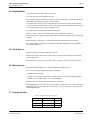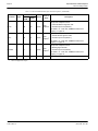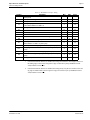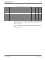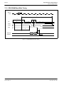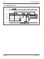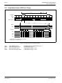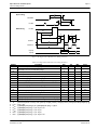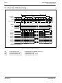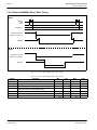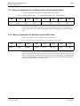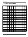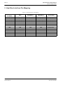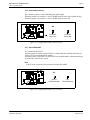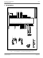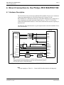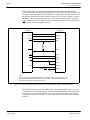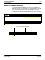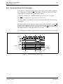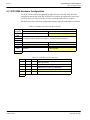
1
S1D13504 Color Graphics LCD/CRT Controller S1D13504 TECHNICAL MANUAL Document Number: X19A-Q-002-14 Copyright © 1997, 2001 Epson Research and Development, Inc. All Rights Reserved. Information in this document is subject to change without notice. You may download and use this document, but only for your own use in evaluating Seiko Epson/EPSON products. You may not modify the document. Epson Research and Development, Inc. disclaims any representation that the contents of this document are accurate or current. The Programs/Technologies described in this document may contain material protected under U.S. and/or International Patent laws. EPSON is a registered trademark of Seiko Epson Corporation. All other trademarks are the property of their respective owners. Page 2 Epson Research and Development Vancouver Design Center THIS PAGE LEFT BLANK S1D13504 X19A-Q-002-14 TECHNICAL MANUAL Issue Date: 01/04/18 Epson Research and Development Vancouver Design Center Page 3 Customer Support Information Comprehensive Support Tools Seiko Epson Corp. provides to the system designer and computer OEM manufacturer a complete set of resources and tools for the development of graphics systems. Evaluation / Demonstration Board • Assembled and fully tested graphics evaluation board with installation guide and schematics. • To borrow an evaluation board, please contact your local Seiko Epson Corp. sales representative. Chip Documentation • Technical manual includes Data Sheet, Application Notes, and Programmer’s Reference. Software • OEM Utilities. • User Utilities. • Evaluation Software. • To obtain these programs, contact Application Engineering Support. Application Engineering Support Engineering and Sales Support is provided by: Japan Seiko Epson Corporation Electronic Devices Marketing Division 421-8, Hino, Hino-shi Tokyo 191-8501, Japan Tel: 042-587-5812 Fax: 042-587-5564 http://www.epson.co.jp Hong Kong Epson Hong Kong Ltd. 20/F., Harbour Centre 25 Harbour Road Wanchai, Hong Kong Tel: 2585-4600 Fax: 2827-4346 TECHNICAL MANUAL Issue Date: 01/04/18 North America Epson Electronics America, Inc. 150 River Oaks Parkway San Jose, CA 95134, USA Tel: (408) 922-0200 Fax: (408) 922-0238 http://www.eea.epson.com Taiwan Epson Taiwan Technology & Trading Ltd. 10F, No. 287 Nanking East Road Sec. 3, Taipei, Taiwan Tel: 02-2717-7360 Fax: 02-2712-9164 Europe Epson Europe Electronics GmbH Riesstrasse 15 80992 Munich, Germany Tel: 089-14005-0 Fax: 089-14005-110 Singapore Epson Singapore Pte., Ltd. No. 1 Temasek Avenue #36-00 Millenia Tower Singapore, 039192 Tel: 337-7911 Fax: 334-2716 S1D13504 X19A-Q-002-14 Page 4 Epson Research and Development Vancouver Design Center THIS PAGE LEFT BLANK S1D13504 X19A-Q-002-14 TECHNICAL MANUAL Issue Date: 01/04/18 ENERGY S AV I NG EPSON GRAPHICS S1D13504 S1D13504 COLOR GRAPHICS LCD/CRT CONTROLLER February 2001 ■ DESCRIPTION The S1D13504 is a low cost, low power, color/monochrome LCD/CRT controller interfacing to a wide range of CPUs and LCDs. The S1D13504 architecture is designed to meet the requirements of embedded markets such as Office Automation equipment, Mobile Communications devices and Hand-Held PCs where Windows CE may serve as a primary operating system. The S1D13504 supports LCD interfaces with data widths up to 16-bits. Using Frame Rate Modulation (FRM), it can display 16 shades of gray on monochrome LCD panels, up to 4096 colors on passive color LCD, and 64K colors on active matrix TFT LCD panels. CRT support is handled through the use of an external RAMDAC interface allowing simultaneous display of both the CRT and LCD panel. A 16-bit memory interface supports up to 2M bytes of FPMDRAM or EDO-DRAM. Supports flexible operating voltages from 2.7V to 5.5V. ■ FEATURES Memory Interface • 16-bit EDO-DRAM or FPM-DRAM interface. • Memory size options: 512K bytes using one 256K×16 device. 2M bytes using one 1M×16 device. • Addressable as a single linear address space. CPU Interface • Supports the following interfaces: Hitachi SH-3. Motorola M68K. ISA bus. MPU bus interface with programmable READY. i386/486 bus. Philips MIPS PR31500/31700. NEC MIPS VR4102. • CPU write buffer. Display Support • 4/8-bit monochrome passive LCD interface. • 4/8/16-bit color passive LCD interface. • Single-panel, single-drive displays. • Dual-panel, dual-drive displays. • Direct support for 9/12-bit TFT; 18-bit TFT is supported up to 64K color depth (16-bit data). • External RAMDAC support using the upper byte of the LCD data bus for the RAMDAC pixel data bus. • Simultaneous display of CRT and 4/8-bit passive or 9-bit TFT panels, regardless of resolution. • Maximum resolution of 800x600 pixels at a color depth of 16 bpp. X19A-C-002-11 Display Modes • 1/2/4/8/16 bit-per-pixel (bpp) support on LCD. • 1/2/4/8 bit-per-pixel (bpp) on CRT. • Up to 16 shades of gray using FRM on monochrome passive LCD panels. • Up to 4096 colors on passive LCD panels. • Up to 64K colors on active matrix TFT LCD in 16 bpp modes. • Split Screen Display: allows two different images to be simultaneously displayed. • Virtual Display Support: displays images larger than the panel size through the use of panning. • Double Buffering/multi-pages: provides smooth animation and instantaneous screen update. • Acceleration of screen updates by allocating full display buffer bandwidth to CPU. Clock Source • Single clock input for both pixel and memory clocks. • Memory clock can be input clock or (input clock/2), providing flexibility to use CPU bus clock as input. • Pixel clock can be memory clock or (memory clock/ 2), (memory clock/3) or (memory clock/4). Power Down Modes • Two power down modes: one software / one hardware. • LCD Power Sequencing. General Purpose IO pins • Up to 12 General Purpose IO pins are available. Operating Voltage • 2.7 volts to 5.5 volts. Package • 128-pin QFP15 surface mount package • 144-pin QFP20 surface mount package 1 GRAPHICS S1D13504 ■ SYSTEM BLOCK DIAGRAM RAMDAC EDO-DRAM FPM-DRAM Analog Out CRT Control CPU Clock S1D13504 Digital Out Flat Panel CONTACT YOUR SALES REPRESENTATIVE FOR THESE COMPREHENSIVE DESIGN TOOLS: • S1D13504 Technical Manual • S5U13504 Evaluation Boards • Windows CE Display Driver • CPU Independent Software Utilities Japan Seiko Epson Corporation Electronic Devices Marketing Division 421-8, Hino, Hino-shi Tokyo 191-8501, Japan Tel: 042-587-5812 Fax: 042-587-5564 http://www.epson.co.jp Hong Kong Epson Hong Kong Ltd. 20/F., Harbour Centre 25 Harbour Road Wanchai, Hong Kong Tel: 2585-4600 Fax: 2827-4346 FOR SYSTEM INTEGRATION SERVICES FOR WINDOWS® CE CONTACT: Epson Research & Development, Inc. Suite #320 - 11120 Horseshoe Way Richmond, B.C., Canada V7A 5H7 Tel: (604) 275-5151 Fax: (604) 275-2167 Email: [email protected] http://www.erd.epson.com North America Epson Electronics America, Inc. 150 River Oaks Parkway San Jose, CA 95134, USA Tel: (408) 922-0200 Fax: (408) 922-0238 http://www.eea.epson.com.com Taiwan, R.O.C. Epson Taiwan Technology & Trading Ltd. 10F, No. 287 Nanking East Road Sec. 3, Taipei, Taiwan, R.O.C. Tel: 02-2717-7360 Fax: 02-2712-9164 Europe Epson Europe Electronics GmbH Riesstrasse 15 80992 Munich, Germany Tel: 089-14005-0 Fax: 089-14005-110 Singapore Epson Singapore Pte., Ltd. No. 1 Temasek Avenue #36-00 Millenia Tower Singapore, 039192 Tel: 337-7911 Fax: 334-2716 Copyright ©1997, 2001 Epson Research and Development, Inc. All rights reserved. VDC Information in this document is subject to change without notice. You may download and use this document, but only for your own use in evaluating Seiko Epson/ EPSON products. You may not modify the document. Epson Research and Development, Inc. disclaims any representation that the contents of this document are accurate or current. The Programs/Technologies described in this document may contain material protected under U.S. and/or International Patent laws. EPSON is a registered trademark of Seiko Epson Corporation. Microsoft, Windows, and the Windows CE Logo are registered trademarks of Microsoft Corporation. 2 X19A-C-002-11 S1D13504 Color Graphics LCD/CRT Controller Hardware Functional Specification Document Number: X19A-A-002-19 Copyright © 1997, 2001 Epson Research and Development, Inc. All Rights Reserved. Information in this document is subject to change without notice. You may download and use this document, but only for your own use in evaluating Seiko Epson/EPSON products. You may not modify the document. Epson Research and Development, Inc. disclaims any representation that the contents of this document are accurate or current. The Programs/Technologies described in this document may contain material protected under U.S. and/or International Patent laws. EPSON is a registered trademark of Seiko Epson Corporation. All other trademarks are the property of their respective owners. Page 2 Epson Research and Development Vancouver Design Center THIS PAGE LEFT BLANK S1D13504 X19A-A-002-19 Hardware Functional Specification Issue Date: 01/11/06 Epson Research and Development Vancouver Design Center Page 3 Table of Contents 1 2 Introduction . . . . . . . . . . . . . . . . . . . . . . . . . . . . . . . . . . . . . . . . . . . . 11 1.1 Scope . . . . . . . . . . . . . . . . . . . . . . . . . . . . . . . . . . . . . 11 1.2 Overview Description . . . . . . . . . . . . . . . . . . . . . . . . . . . . . . . 11 Features . . . . . . . . . . . . . . . . . . . . . . . . . . . . . . . . . . . . . . . . . . . . . . 12 2.1 Memory Interface . . . . . . . . . . . . . . . . . . . . . . . . . . . . . . . . . 12 2.2 CPU Interface . . . . . . . . . . . . . . . . . . . . . . . . . . . . . . . . . . 12 2.3 Display Support 2.4 Display Modes . . . . . . . . . . . . . . . . . . . . . . . . . . . . . . . . . . 13 . . . . . . . . . . . . . . . . . . . . . . . . . . . . . . . . . 12 2.5 Clock Source 2.6 Miscellaneous . . . . . . . . . . . . . . . . . . . . . . . . . . . . . . . . . . 13 2.7 Package and Pin . . . . . . . . . . . . . . . . . . . . . . . . . . . . . . . . . . 13 . . . . . . . . . . . . . . . . . . . . . . . . . . . . . . . . . 13 3 Typical System Implementation Diagrams . . . . . . . . . . . . . . . . . . . . . . . . . . . 14 4 Block Description 4.1 4.2 5 . . . . . . . . . . . . . . . . . . . . . . . . . . . . . . . . . . . . . . . . 16 Functional Block Diagram . . . . . . . . . . . . . . . . . . . . . . . . . . . . . 16 Functional Block Descriptions . . . . . . . . . . . . . . . . . . . . . . . . . . . . 17 4.2.1 Host Interface . . . . . . . . . . . . . . . . . . . . . . . . . . . . . . . . . . . . . . . . . . 17 4.2.2 Memory Controller . . . . . . . . . . . . . . . . . . . . . . . . . . . . . . . . . . . . . . . 17 4.2.3 Display FIFO . . . . . . . . . . . . . . . . . . . . . . . . . . . . . . . . . . . . . . . . . . 17 4.2.4 Look-Up Table 4.2.5 LCD Interface . . . . . . . . . . . . . . . . . . . . . . . . . . . . . . . . . . . . . . . . . . 17 . . . . . . . . . . . . . . . . . . . . . . . . . . . . . . . . . . . . . . . . . 17 4.2.6 Power Save . . . . . . . . . . . . . . . . . . . . . . . . . . . . . . . . . . . . . . . . . . . 17 Pin Out . . . . . . . . . . . . . . . . . . . . . . . . . . . . . . . . . . . . . . . . . . . . . . 18 5.1 Pinout Diagram for S1D13504F00A . . . . . . . . . . . . . . . . . . . . . . . . . 18 5.2 Pinout Diagram for S1D13504F01A . . . . . . . . . . . . . . . . . . . . . . . . . 19 5.3 Pinout Diagram for S1D13504F02A . . . . . . . . . . . . . . . . . . . . . . . . . 20 5.4 Pin Description . . . . . . . . . . . . . . . . . . . . . . . . . . . . . . . . . . 21 5.4.1 Host Interface . . . . . . . . . . . . . . . . . . . . . . . . . . . . . . . . . . . . . . . . . . 21 5.4.2 Memory Interface . . . . . . . . . . . . . . . . . . . . . . . . . . . . . . . . . . . . . . . . 24 5.4.3 LCD Interface . . . . . . . . . . . . . . . . . . . . . . . . . . . . . . . . . . . . . . . . . . 26 5.4.4 Clock Input . . . . . . . . . . . . . . . . . . . . . . . . . . . . . . . . . . . . . . . . . . . 26 5.4.5 CRT and External RAMDAC Interface . . . . . . . . . . . . . . . . . . . . . . . . . . . . . 27 5.4.6 Miscellaneous . . . . . . . . . . . . . . . . . . . . . . . . . . . . . . . . . . . . . . . . . . 29 5.4.7 Power Supply . . . . . . . . . . . . . . . . . . . . . . . . . . . . . . . . . . . . . . . . . . 29 5.5 Summary of Configuration Options . . . . . . . . . . . . . . . . . . . . . . . . . . 30 5.6 Multiple Function Pin Mapping . . . . . . . . . . . . . . . . . . . . . . . . . . . 31 6 D.C. Characteristics . . . . . . . . . . . . . . . . . . . . . . . . . . . . . . . . . . . . . . . 34 7 A.C. Characteristics . . . . . . . . . . . . . . . . . . . . . . . . . . . . . . . . . . . . . . . 36 7.1 CPU Interface Timing . . . . . . . . . . . . . . . . . . . . . . . . . . . . . . . 36 7.1.1 SH-3 Interface Timing . . . . . . . . . . . . . . . . . . . . . . . . . . . . . . . . . . . . . . 36 Hardware Functional Specification Issue Date: 01/11/06 S1D13504 X19A-A-002-19 Page 4 Epson Research and Development Vancouver Design Center 7.1.2 MC68K Bus 1 Interface Timing (e.g. MC68000) . . . . . . . . . . . . . . . . . . . . . . . .38 7.1.3 MC68K Bus 2 Interface Timing (e.g. MC68030) . . . . . . . . . . . . . . . . . . . . . . . .40 7.1.4 Generic MPU Interface Synchronous Timing . . . . . . . . . . . . . . . . . . . . . . . . . .42 7.1.5 Generic MPU Interface Asynchronous Timing . . . . . . . . . . . . . . . . . . . . . . . . .44 7.2 Clock Input Requirements . . . . . . . . . . . . . . . . . . . . . . . . . . . . . 46 7.3 Memory Interface Timing . . . . . . . . . . . . . . . . . . . . . . . . . . . . . 46 7.3.1 EDO-DRAM Read Timing . . . . . . . . . . . . . . . . . . . . . . . . . . . . . . . . . . . .46 7.3.2 EDO-DRAM Write Timing . . . . . . . . . . . . . . . . . . . . . . . . . . . . . . . . . . .48 7.3.3 EDO-DRAM Read-Write Timing . . . . . . . . . . . . . . . . . . . . . . . . . . . . . . . .50 7.3.4 EDO-DRAM CAS Before RAS Refresh Timing . . . . . . . . . . . . . . . . . . . . . . . .52 7.3.5 EDO-DRAM Self-Refresh Timing . . . . . . . . . . . . . . . . . . . . . . . . . . . . . . . .53 7.3.6 FPM-DRAM Read Timing . . . . . . . . . . . . . . . . . . . . . . . . . . . . . . . . . . . .54 7.3.7 FPM-DRAM Write Timing . . . . . . . . . . . . . . . . . . . . . . . . . . . . . . . . . . .56 7.3.8 FPM-DRAM Read-Write Timing . . . . . . . . . . . . . . . . . . . . . . . . . . . . . . . .58 7.3.9 FPM-DRAM CAS# Before RAS# Refresh Timing . . . . . . . . . . . . . . . . . . . . . . .60 7.3.10 FPM-DRAM Self-Refresh Timing . . . . . . . . . . . . . . . . . . . . . . . . . . . . . . . .61 7.4 Display Interface . . . . . . . . . . . . . . . . . . . . . . . . . . . . . . . . . 62 7.4.1 8 Power-On/Reset Timing . . . . . . . . . . . . . . . . . . . . . . . . . . . . . . . . . . . . .62 7.4.2 Suspend Timing . . . . . . . . . . . . . . . . . . . . . . . . . . . . . . . . . . . . . . . . .63 7.4.3 Single Monochrome 4-Bit Panel Timing . . . . . . . . . . . . . . . . . . . . . . . . . . . . .64 7.4.4 Single Monochrome 8-Bit Panel Timing . . . . . . . . . . . . . . . . . . . . . . . . . . . . .66 7.4.5 Single Color 4-Bit Panel Timing . . . . . . . . . . . . . . . . . . . . . . . . . . . . . . . . .68 7.4.6 Single Color 8-Bit Panel Timing (Format 1) . . . . . . . . . . . . . . . . . . . . . . . . . . .70 7.4.7 Single Color 8-Bit Panel Timing (Format 2) . . . . . . . . . . . . . . . . . . . . . . . . . . .72 7.4.8 Single Color 16-Bit Panel Timing . . . . . . . . . . . . . . . . . . . . . . . . . . . . . . . .74 7.4.9 Dual Monochrome 8-Bit Panel Timing . . . . . . . . . . . . . . . . . . . . . . . . . . . . .76 7.4.10 Dual Color 8-Bit Panel Timing . . . . . . . . . . . . . . . . . . . . . . . . . . . . . . . . . .78 7.4.11 Dual Color 16-Bit Panel Timing . . . . . . . . . . . . . . . . . . . . . . . . . . . . . . . . .80 7.4.12 16-Bit TFT Panel Timing . . . . . . . . . . . . . . . . . . . . . . . . . . . . . . . . . . . .82 7.4.13 CRT Timing . . . . . . . . . . . . . . . . . . . . . . . . . . . . . . . . . . . . . . . . . . .85 7.4.14 External RAMDAC Read / Write Timing . . . . . . . . . . . . . . . . . . . . . . . . . . . .88 Registers . . . . . . . . . . . . . . . . . . . . . . . . . . . . . . . . . . . . . . . . . . . . . 89 8.1 Register Mapping 8.2 Register Descriptions . . . . . . . . . . . . . . . . . . . . . . . . . . . . . . . 89 . . . . . . . . . . . . . . . . . . . . . . . . . . . . . . . . 89 8.2.1 Revision Code Register . . . . . . . . . . . . . . . . . . . . . . . . . . . . . . . . . . . . .89 8.2.2 Memory Configuration Registers . . . . . . . . . . . . . . . . . . . . . . . . . . . . . . . .90 8.2.3 Panel/Monitor Configuration Registers . . . . . . . . . . . . . . . . . . . . . . . . . . . . .91 8.2.4 Display Configuration Registers . . . . . . . . . . . . . . . . . . . . . . . . . . . . . . . . .96 8.2.5 Clock Configuration Register . . . . . . . . . . . . . . . . . . . . . . . . . . . . . . . . . 101 8.2.6 Power Save Configuration Registers . . . . . . . . . . . . . . . . . . . . . . . . . . . . . . 101 8.2.7 Miscellaneous Registers . . . . . . . . . . . . . . . . . . . . . . . . . . . . . . . . . . . . 102 8.2.8 Look-Up Table Registers . . . . . . . . . . . . . . . . . . . . . . . . . . . . . . . . . . . . 110 S1D13504 X19A-A-002-19 Hardware Functional Specification Issue Date: 01/11/06 Epson Research and Development Vancouver Design Center 8.2.9 9 Page 5 External RAMDAC Control Registers . . . . . . . . . . . . . . . . . . . . . . . . . . . . 111 Display Buffer . . . . . . . . . . . . . . . . . . . . . . . . . . . . . . . . . . . . . . . . . . .113 9.1 Image Buffer . . . . . . . . . . . . . . . . . . . . . . . . . . . . . . . . . . .114 9.2 Half Frame Buffer . . . . . . . . . . . . . . . . . . . . . . . . . . . . . . . .114 10 Display Configuration . . . . . . . . . . . . . . . . . . . . . . . . . . . . . . . . . . . . . .115 10.1 Display Mode Data Format . . . . . . . . . . . . . . . . . . . . . . . . . . . . .115 10.2 Image Manipulation . . . . . . . . . . . . . . . . . . . . . . . . . . . . . . . .117 11 Clocking . . . . . . . . . . . . . . . . . . . . . . . . . . . . . . . . . . . . . . . . . . . . . .118 11.1 Maximum MCLK: PCLK Ratios . . . . . . . . . . . . . . . . . . . . . . . . . . .118 11.2 Frame Rate Calculation . . . . . . . . . . . . . . . . . . . . . . . . . . . . . .119 12 Look-Up Table Architecture . . . . . . . . . . . . . . . . . . . . . . . . . . . . . . . . . . .121 12.1 Gray Shade Display Modes . . . . . . . . . . . . . . . . . . . . . . . . . . . . .121 12.2 Color Display Modes . . . . . . . . . . . . . . . . . . . . . . . . . . . . . . .123 13 Power Save Modes . . . . . . . . . . . . . . . . . . . . . . . . . . . . . . . . . . . . . . . .127 13.1 Hardware Suspend . . . . . . . . . . . . . . . . . . . . . . . . . . . . . . . .127 13.2 Software Suspend . . . . . . . . . . . . . . . . . . . . . . . . . . . . . . . . .127 13.3 Power Save Mode Function Summary . . . . . . . . . . . . . . . . . . . . . . . . .128 13.4 Pin States in Power Save Modes . . . . . . . . . . . . . . . . . . . . . . . . . . .128 14 Mechanical Data . . . . . . . . . . . . . . . . . . . . . . . . . . . . . . . . . . . . . . . . .129 14.1 QFP15-128 (S1D13504F00A) . . . . . . . . . . . . . . . . . . . . . . . . . . . .129 14.2 TQFP15-128 (S1D13504F01A) . . . . . . . . . . . . . . . . . . . . . . . . . . .130 14.3 QFP20-144 (S1D13504F02A) . . . . . . . . . . . . . . . . . . . . . . . . . . . .131 15 References . . . . . . . . . . . . . . . . . . . . . . . . . . . . . . . . . . . . . . . . . . . .132 16 Sales and Technical Support . . . . . . . . . . . . . . . . . . . . . . . . . . . . . . . . . .133 Hardware Functional Specification Issue Date: 01/11/06 S1D13504 X19A-A-002-19 Page 6 Epson Research and Development Vancouver Design Center THIS PAGE LEFT BLANK S1D13504 X19A-A-002-19 Hardware Functional Specification Issue Date: 01/11/06 Epson Research and Development Vancouver Design Center Page 7 List of Tables Table 2-1: S1D13504 Series Package list . . . . . . . . . . . . . . . . . . . . . . . . . . . . . . . . . . . . 13 Table 5-1: Host Interface Pin Descriptions . . . . . . . . . . . . . . . . . . . . . . . . . . . . . . . . . . . 21 Table 5-2: Memory Interface Pin Descriptions . . . . . . . . . . . . . . . . . . . . . . . . . . . . . . . . . 24 Table 5-3: LCD Interface Pin Descriptions . . . . . . . . . . . . . . . . . . . . . . . . . . . . . . . . . . . 26 Table 5-4: Clock Input Pin Description . . . . . . . . . . . . . . . . . . . . . . . . . . . . . . . . . . . . . 26 Table 5-5: CRT and RAMDAC Interface Pin Descriptions . . . . . . . . . . . . . . . . . . . . . . . . . . . 27 Table 5-6: Miscellaneous Pin Descriptions . . . . . . . . . . . . . . . . . . . . . . . . . . . . . . . . . . . 29 Table 5-7: Power Supply Pin Descriptions . . . . . . . . . . . . . . . . . . . . . . . . . . . . . . . . . . . 29 Table 5-8: Summary of Power On / Reset Options . . . . . . . . . . . . . . . . . . . . . . . . . . . . . . . 30 Table 5-9: Host Bus Interface Pin Mapping . . . . . . . . . . . . . . . . . . . . . . . . . . . . . . . . . . . 31 Table 5-10: Memory Interface Pin Mapping . . . . . . . . . . . . . . . . . . . . . . . . . . . . . . . . . . . 32 Table 5-11: LCD, CRT, RAMDAC Interface Pin Mapping . . . . . . . . . . . . . . . . . . . . . . . . . . . 33 Table 6-1: Absolute Maximum Ratings . . . . . . . . . . . . . . . . . . . . . . . . . . . . . . . . . . . . . 34 Table 6-2: Recommended Operating Conditions . . . . . . . . . . . . . . . . . . . . . . . . . . . . . . . . 34 Table 6-3: Input Specifications . . . . . . . . . . . . . . . . . . . . . . . . . . . . . . . . . . . . . . . . . 34 Table 6-4: Output Specifications . . . . . . . . . . . . . . . . . . . . . . . . . . . . . . . . . . . . . . . . . 35 Table 7-1: SH-3 Interface Timing . . . . . . . . . . . . . . . . . . . . . . . . . . . . . . . . . . . . . . . . 37 Table 7-2: MC68K Bus 1 Interface Timing . . . . . . . . . . . . . . . . . . . . . . . . . . . . . . . . . . . 39 Table 7-3: MC68K Bus 2 Interface Timing . . . . . . . . . . . . . . . . . . . . . . . . . . . . . . . . . . . 41 Table 7-4: Generic MPU Interface Synchronous Timing . . . . . . . . . . . . . . . . . . . . . . . . . . . . 43 Table 7-5: Generic MPU Interface Asynchronous Timing . . . . . . . . . . . . . . . . . . . . . . . . . . . 45 Table 7-6: Clock Input Requirements . . . . . . . . . . . . . . . . . . . . . . . . . . . . . . . . . . . . . . 46 Table 7-7: EDO DRAM Read Timing . . . . . . . . . . . . . . . . . . . . . . . . . . . . . . . . . . . . . . 47 Table 7-8: EDO DRAM Write Timing . . . . . . . . . . . . . . . . . . . . . . . . . . . . . . . . . . . . . 49 Table 7-9: EDO DRAM Read-Write Timing . . . . . . . . . . . . . . . . . . . . . . . . . . . . . . . . . . 51 Table 7-10: EDO-DRAM CAS Before RAS Refresh Timing . . . . . . . . . . . . . . . . . . . . . . . . . . 52 Table 7-11: EDO-DRAM Self-Refresh Timing . . . . . . . . . . . . . . . . . . . . . . . . . . . . . . . . . . 53 Table 7-12: FPM DRAM Read Timing . . . . . . . . . . . . . . . . . . . . . . . . . . . . . . . . . . . . . . 55 Table 7-13: FPM-DRAM Write Timing . . . . . . . . . . . . . . . . . . . . . . . . . . . . . . . . . . . . . 57 Table 7-14: FPM-DRAM Read-Write Timing . . . . . . . . . . . . . . . . . . . . . . . . . . . . . . . . . . 59 Table 7-15: FPM-DRAM CAS# Before RAS# Refresh Timing . . . . . . . . . . . . . . . . . . . . . . . . . 60 Table 7-16: FPM-DRAM CBR Self-Refresh Timing . . . . . . . . . . . . . . . . . . . . . . . . . . . . . . . 61 Table 7-17: LCD Panel Power-On/Reset Timing . . . . . . . . . . . . . . . . . . . . . . . . . . . . . . . . . 62 Table 7-18: LCD Panel Suspend Timing . . . . . . . . . . . . . . . . . . . . . . . . . . . . . . . . . . . . . 63 Table 7-19: Single Monochrome 4-Bit Panel A.C. Timing . . . . . . . . . . . . . . . . . . . . . . . . . . . . 65 Table 7-20: Single Monochrome 8-Bit Panel A.C. Timing . . . . . . . . . . . . . . . . . . . . . . . . . . . . 67 Table 7-21: Single Color 4-Bit Panel A.C. Timing . . . . . . . . . . . . . . . . . . . . . . . . . . . . . . . . 69 Table 7-22: Single Color 8-Bit Panel A.C. Timing (Format 1) . . . . . . . . . . . . . . . . . . . . . . . . . . 71 Table 7-23: Single Color 8-Bit Panel A.C. Timing (Format 2) . . . . . . . . . . . . . . . . . . . . . . . . . . 73 Table 7-24: Single Color 16-Bit Panel A.C. Timing . . . . . . . . . . . . . . . . . . . . . . . . . . . . . . . 75 Hardware Functional Specification Issue Date: 01/11/06 S1D13504 X19A-A-002-19 Page 8 Epson Research and Development Vancouver Design Center Table 7-25: Dual Monochrome 8-Bit Panel A.C. Timing . . . . . . . . . . . . . . . . . . . . . . . . . . . . .77 Table 7-26: Dual Color 8-Bit Panel A.C. Timing . . . . . . . . . . . . . . . . . . . . . . . . . . . . . . . . .79 Table 7-27: Dual Color 16-Bit Panel A.C. Timing . . . . . . . . . . . . . . . . . . . . . . . . . . . . . . . .81 Table 7-28: TFT A.C. Timing . . . . . . . . . . . . . . . . . . . . . . . . . . . . . . . . . . . . . . . . . . .84 Table 7-29: CRT A.C. Timing . . . . . . . . . . . . . . . . . . . . . . . . . . . . . . . . . . . . . . . . . . .87 Table 7-30: Generic Bus RAMDAC Read / Write Timing . . . . . . . . . . . . . . . . . . . . . . . . . . . .88 Table 8-1: S1D13504 Addressing . . . . . . . . . . . . . . . . . . . . . . . . . . . . . . . . . . . . . . . .89 Table 8-2: DRAM Refresh Rate Selection . . . . . . . . . . . . . . . . . . . . . . . . . . . . . . . . . . . .90 Table 8-3: Panel Data Width Selection . . . . . . . . . . . . . . . . . . . . . . . . . . . . . . . . . . . . . .91 Table 8-4: FPLINE Polarity Selection . . . . . . . . . . . . . . . . . . . . . . . . . . . . . . . . . . . . . .93 Table 8-5: FPFRAME Polarity Selection . . . . . . . . . . . . . . . . . . . . . . . . . . . . . . . . . . . . .95 Table 8-6: Simultaneous Display Option Selection . . . . . . . . . . . . . . . . . . . . . . . . . . . . . . .96 Table 8-7: Number of Bits-Per-Pixel Selection . . . . . . . . . . . . . . . . . . . . . . . . . . . . . . . . . .97 Table 8-8: Pixel Panning Selection . . . . . . . . . . . . . . . . . . . . . . . . . . . . . . . . . . . . . . . 100 Table 8-9: PCLK Divide Selection . . . . . . . . . . . . . . . . . . . . . . . . . . . . . . . . . . . . . . . 101 Table 8-10: Suspend Refresh Selection . . . . . . . . . . . . . . . . . . . . . . . . . . . . . . . . . . . . . 101 Table 8-11: Minimum Memory Timing Selection . . . . . . . . . . . . . . . . . . . . . . . . . . . . . . . . 107 Table 8-12: RAS-to-CAS Delay Timing Select . . . . . . . . . . . . . . . . . . . . . . . . . . . . . . . . . 108 Table 8-13: RAS Precharge Timing Select . . . . . . . . . . . . . . . . . . . . . . . . . . . . . . . . . . . 108 Table 8-14: Optimal NRC, NRP, and NRCD Values at Maximum MCLK Frequency . . . . . . . . . . . . . 109 Table 8-15: RGB Index Selection . . . . . . . . . . . . . . . . . . . . . . . . . . . . . . . . . . . . . . . . 110 Table 9-1: S1D13504 Addressing . . . . . . . . . . . . . . . . . . . . . . . . . . . . . . . . . . . . . . . 113 Table 11-1: Maximum PCLK Frequency with EDO-DRAM . . . . . . . . . . . . . . . . . . . . . . . . . . 118 Table 11-2: Maximum PCLK Frequency with FPM-DRAM . . . . . . . . . . . . . . . . . . . . . . . . . . 118 Table 11-3: Example Frame Rates . . . . . . . . . . . . . . . . . . . . . . . . . . . . . . . . . . . . . . . . 119 Table 12-1: Look-Up Table Configurations . . . . . . . . . . . . . . . . . . . . . . . . . . . . . . . . . . . 121 Table 13-1: Power Save Mode Function Summary . . . . . . . . . . . . . . . . . . . . . . . . . . . . . . . 128 Table 13-2: Pin States in Power Save Modes . . . . . . . . . . . . . . . . . . . . . . . . . . . . . . . . . . 128 S1D13504 X19A-A-002-19 Hardware Functional Specification Issue Date: 01/11/06 Epson Research and Development Vancouver Design Center Page 9 List of Figures Figure 3-1: Typical System Diagram – SH-3 Bus, 1Mx16 FPM/EDO-DRAM . . . . . . . . . . . . . . . . . 14 Figure 3-2: Typical System Diagram – MC68K Bus 1, 1Mx16 FPM/EDO-DRAM (16-Bit MC68000) . . . . 14 Figure 3-3: Typical System Diagram – MC68K Bus 2, 256Kx16 FPM/EDO-DRAM (32-Bit MC68030) . . 15 Figure 3-4: Typical System Diagram – Generic Bus, 1Mx16 FPM/EDO-DRAM . . . . . . . . . . . . . . . 15 Figure 4-1: System Block Diagram Showing Datapaths . . . . . . . . . . . . . . . . . . . . . . . . . . . . 16 Figure 5-1: Pinout Diagram of F00A . . . . . . . . . . . . . . . . . . . . . . . . . . . . . . . . . . . . . . 18 Figure 5-2: Pinout Diagram of F01A . . . . . . . . . . . . . . . . . . . . . . . . . . . . . . . . . . . . . . 19 Figure 5-3: Pinout Diagram of F02A . . . . . . . . . . . . . . . . . . . . . . . . . . . . . . . . . . . . . . 20 Figure 7-1: SH-3 Interface Timing . . . . . . . . . . . . . . . . . . . . . . . . . . . . . . . . . . . . . . . 36 Figure 7-2: MC68K Bus 1 Interface Timing . . . . . . . . . . . . . . . . . . . . . . . . . . . . . . . . . . 38 Figure 7-3: MC68K Bus 2 Interface Timing . . . . . . . . . . . . . . . . . . . . . . . . . . . . . . . . . . 40 Figure 7-4: Generic MPU Interface Synchronous Timing . . . . . . . . . . . . . . . . . . . . . . . . . . . 42 Figure 7-5: Generic MPU Interface Asynchronous Timing . . . . . . . . . . . . . . . . . . . . . . . . . . . 44 Figure 7-6: Clock Input Requirements . . . . . . . . . . . . . . . . . . . . . . . . . . . . . . . . . . . . . 46 Figure 7-7: EDO-DRAM Read Timing . . . . . . . . . . . . . . . . . . . . . . . . . . . . . . . . . . . . . 46 Figure 7-8: EDO-DRAM Write Timing . . . . . . . . . . . . . . . . . . . . . . . . . . . . . . . . . . . . . 48 Figure 7-9: EDO-DRAM Read-Write Timing . . . . . . . . . . . . . . . . . . . . . . . . . . . . . . . . . 50 Figure 7-10: EDO-DRAM CAS Before RAS Refresh Timing . . . . . . . . . . . . . . . . . . . . . . . . . . 52 Figure 7-11: EDO-DRAM Self-Refresh Timing . . . . . . . . . . . . . . . . . . . . . . . . . . . . . . . . . 53 Figure 7-12: FPM-DRAM Read Timing . . . . . . . . . . . . . . . . . . . . . . . . . . . . . . . . . . . . . 54 Figure 7-13: FPM-DRAM Write Timing . . . . . . . . . . . . . . . . . . . . . . . . . . . . . . . . . . . . . 56 Figure 7-14: FPM-DRAM Read-Write Timing . . . . . . . . . . . . . . . . . . . . . . . . . . . . . . . . . . 58 Figure 7-15: FPM-DRAM CAS# Before RAS# Refresh Timing . . . . . . . . . . . . . . . . . . . . . . . . 60 Figure 7-16: FPM-DRAM CBR Self-Refresh Timing . . . . . . . . . . . . . . . . . . . . . . . . . . . . . . 61 Figure 7-17: LCD Panel Power-On/Reset Timing . . . . . . . . . . . . . . . . . . . . . . . . . . . . . . . . 62 Figure 7-18: LCD Panel Suspend Timing . . . . . . . . . . . . . . . . . . . . . . . . . . . . . . . . . . . . 63 Figure 7-19: Single Monochrome 4-Bit Panel Timing . . . . . . . . . . . . . . . . . . . . . . . . . . . . . . 64 Figure 7-20: Single Monochrome 4-Bit Panel A.C. Timing . . . . . . . . . . . . . . . . . . . . . . . . . . . 65 Figure 7-21: Single Monochrome 8-Bit Panel Timing . . . . . . . . . . . . . . . . . . . . . . . . . . . . . . 66 Figure 7-22: Single Monochrome 8-Bit Panel A.C. Timing . . . . . . . . . . . . . . . . . . . . . . . . . . . 67 Figure 7-23: Single Color 4-Bit Panel Timing . . . . . . . . . . . . . . . . . . . . . . . . . . . . . . . . . . 68 Figure 7-24: Single Color 4-Bit Panel A.C. Timing . . . . . . . . . . . . . . . . . . . . . . . . . . . . . . . 69 Figure 7-25: Single Color 8-Bit Panel Timing (Format 1) . . . . . . . . . . . . . . . . . . . . . . . . . . . . 70 Figure 7-26: Single Color 8-Bit Panel A.C. Timing (Format 1) . . . . . . . . . . . . . . . . . . . . . . . . . 71 Figure 7-27: Single Color 8-Bit Panel Timing (Format 2) . . . . . . . . . . . . . . . . . . . . . . . . . . . . 72 Figure 7-28: Single Color 8-Bit Panel A.C. Timing (Format 2) . . . . . . . . . . . . . . . . . . . . . . . . . 73 Figure 7-29: Single Color 16-Bit Panel Timing . . . . . . . . . . . . . . . . . . . . . . . . . . . . . . . . . 74 Figure 7-30: Single Color 16-Bit Panel A.C. Timing . . . . . . . . . . . . . . . . . . . . . . . . . . . . . . . 75 Figure 7-31: Dual Monochrome 8-Bit Panel Timing . . . . . . . . . . . . . . . . . . . . . . . . . . . . . . . 76 Figure 7-32: Dual Monochrome 8-Bit Panel A.C. Timing . . . . . . . . . . . . . . . . . . . . . . . . . . . . 77 Hardware Functional Specification Issue Date: 01/11/06 S1D13504 X19A-A-002-19 Page 10 Epson Research and Development Vancouver Design Center Figure 7-33: Dual Color 8-Bit Panel Timing . . . . . . . . . . . . . . . . . . . . . . . . . . . . . . . . . . . 78 Figure 7-34: Dual Color 8-Bit Panel A.C. Timing . . . . . . . . . . . . . . . . . . . . . . . . . . . . . . . . 79 Figure 7-35: Dual Color 16-Bit Panel Timing . . . . . . . . . . . . . . . . . . . . . . . . . . . . . . . . . . . 80 Figure 7-36: Dual Color 16-Bit Panel A.C. Timing . . . . . . . . . . . . . . . . . . . . . . . . . . . . . . . . 81 Figure 7-37: 16-Bit TFT Panel Timing . . . . . . . . . . . . . . . . . . . . . . . . . . . . . . . . . . . . . . 82 Figure 7-38: TFT A.C. Timing . . . . . . . . . . . . . . . . . . . . . . . . . . . . . . . . . . . . . . . . . . 83 Figure 7-39: CRT Timing . . . . . . . . . . . . . . . . . . . . . . . . . . . . . . . . . . . . . . . . . . . . . 85 Figure 7-40: CRT A.C. Timing . . . . . . . . . . . . . . . . . . . . . . . . . . . . . . . . . . . . . . . . . . 86 Figure 7-41: Generic Bus RAMDAC Read / Write Timing . . . . . . . . . . . . . . . . . . . . . . . . . . . . 88 Figure 9-1: Display Buffer Addressing . . . . . . . . . . . . . . . . . . . . . . . . . . . . . . . . . . . . 113 Figure 10-1: 1/2/4/8 Bit-Per-Pixel Format Memory Organization . . . . . . . . . . . . . . . . . . . . . . . 115 Figure 10-2: 15/16 Bit-Per-Pixel Format Memory Organization . . . . . . . . . . . . . . . . . . . . . . . . 116 Figure 10-3: Image Manipulation . . . . . . . . . . . . . . . . . . . . . . . . . . . . . . . . . . . . . . . . 117 Figure 12-1: 1 Bit-Per-Pixel – 2-Level Gray-Shade Mode Look-Up Table Architecture . . . . . . . . . . . . 121 Figure 12-2: 2 Bit-Per-Pixel – 4-Level Gray-Shade Mode Look-Up Table Architecture . . . . . . . . . . . . 122 Figure 12-3: 4 Bit-Per-Pixel – 16-Level Gray-Shade Mode Look-Up Table Architecture . . . . . . . . . . . 122 Figure 12-4: 1 Bit-Per-Pixel – 2-Level Color Look-Up Table Architecture . . . . . . . . . . . . . . . . . . 123 Figure 12-5: 2 Bit-Per-Pixel – 4-Level Color Mode Look-Up Table Architecture . . . . . . . . . . . . . . . 124 Figure 12-6: 4 Bit-Per-Pixel – 16-Level Color Mode Look-Up Table Architecture . . . . . . . . . . . . . . 125 Figure 12-7: 8 Bit-Per-Pixel – 256-Level Color Mode Look-Up Table Architecture . . . . . . . . . . . . . . 126 Figure 14-1: Mechanical Drawing QFP15-128 . . . . . . . . . . . . . . . . . . . . . . . . . . . . . . . . . 129 Figure 14-2: Mechanical Drawing TQFP15-128 . . . . . . . . . . . . . . . . . . . . . . . . . . . . . . . . 130 Figure 14-3: Mechanical Drawing QFP20-144 . . . . . . . . . . . . . . . . . . . . . . . . . . . . . . . . . 131 S1D13504 X19A-A-002-19 Hardware Functional Specification Issue Date: 01/11/06 Epson Research and Development Vancouver Design Center Page 11 1 Introduction 1.1 Scope This is the Hardware Functional Specification for the S1D13504 Series Color Graphics LCD/CRT Controller Chip. Included in this document are timing diagrams, AC and DC characteristics, register descriptions, and power management descriptions. This document is intended for two audiences: Video Subsystem Designers and Software Developers. This document is updated as appropriate. Please check for the latest revision of this document before beginning any development. The latest revision can be downloaded at www.erd.epson.com. We appreciate your comments on our documentation. Please contact us via email at [email protected]. 1.2 Overview Description The S1D13504 is a low cost, low power color/monochrome LCD/CRT controller interfacing to a wide range of CPUs and LCDs. The S1D13504 architecture is designed to meet the requirements of embedded markets such as Office Automation equipment, Mobile Communications devices and Hand-Held PCs where Windows CE may serve as a primary operating system. The S1D13504 supports LCD interfaces with data widths up to 16 bits. Using Frame Rate Modulation (FRM), it can display 16 shades of gray on monochrome LCD panels, up to 4096 colors on passive color LCDs, and 64K colors on active matrix TFT LCD panels. CRT support is handled through the use of an external RAMDAC interface allowing simultaneous display of both the CRT and LCD panel. A 16-bit memory interface supports up to 2M bytes of FPM-DRAM or EDODRAM. Flexible operating voltages from 2.7V to 5.5V provide for very low power consumption. Hardware Functional Specification Issue Date: 01/11/06 S1D13504 X19A-A-002-19 Page 12 Epson Research and Development Vancouver Design Center 2 Features 2.1 Memory Interface • 16-bit DRAM interface: • EDO-DRAM up to 40MHz data rate (80M bytes per second). • FPM-DRAM up to 25MHz data rate (50M bytes per second). • Memory size options: • 512K bytes using one 256K×16 device. • 2M bytes using one 1M×16 device. • A configuration register can be programmed to enhance performance by tailoring the memory control output timing to the DRAM device. 2.2 CPU Interface • Supports the following interfaces: • 8/16-bit Hitachi SH-3 bus interface. • 16-bit interface to 16/32-bit Motorola MC68K microprocessors/microcontrollers. • Philips MIPS PR31500 / PR31700. • NEC MIPS VR4102. • 8/16-bit generic interface bus. • One-Stage write buffer for minimum wait-state CPU writes. • Registers are memory-mapped; M/R# pin selects between memory and register address space. • The complete 2M byte display buffer address space is directly and contiguously available through the 21-bit address bus. 2.3 Display Support • 4/8-bit monochrome or 4/8/16-bit color passive LCD interface for single-panel, single-drive displays. • 8-bit monochrome or 8/16-bit color passive LCD interface for dual-panel, dual-drive displays. • Direct support for 9/12-bit TFT, 18/24-bit TFT are supported up to 64K color depth (16-bit data). • External RAMDAC support using the upper byte of the LCD data bus for the RAMDAC pixel data bus. • Simultaneous display of CRT and 4/8-bit passive panel or 9-bit TFT panel: • Normal mode for cases where LCD and CRT image sizes are identical. • Line-Doubling mode for simultaneous display of 240-line images on 240-line LCD and 480line CRT. • Even-Scan and interlace modes for simultaneous display of 480-line images on 240-line LCD and 480-line CRT. S1D13504 X19A-A-002-19 Hardware Functional Specification Issue Date: 01/11/06 Epson Research and Development Vancouver Design Center Page 13 2.4 Display Modes • 1/2/4/8/16 bit-per-pixel modes supported on LCD. • 1/2/4/8 bit-per-pixel modes supported on CRT. • Up to 16 shades of gray by FRM on monochrome passive LCD panels; a 16x4 Look-Up Table is used to map 1/2/4 bit-per-pixel modes into these shades. • Up to 4096 colors on color passive LCD panels; three 16x4 Look-Up Tables are used to map 1/2/4/8 bit-per-pixel modes into these colors, 16 bit-per-pixel mode is mapped directly using the 4 most significant bits of the red, green and blue colors. • Up to 64K colors in 16 bit-per-pixel mode on TFT panels. • Split screen mode – allows two different images to be simultaneously displayed. • Virtual display mode – displays images larger than the panel size through the use of panning and scrolling. • Double buffering / multi-pages – for smooth animation and instantaneous screen update. • Fast-Update feature – accelerates screen update by allocating full display buffer bandwidth to CPU (see REG[23h] bit 7). 2.5 Clock Source • Single clock input for both pixel and memory clocks. • Memory clock can be input clock or (input clock)/2 – this provides flexibility to use CPU bus clock as input clock. • Pixel clock can be memory clock, (memory clock)/2, (memory clock)/3 or (memory clock)/4. 2.6 Miscellaneous • The memory data bus MD[15:0], is used to configure the chip at power-on. • Up to 12 General Purpose Input/Output pins are available: • GPIO0 is always available. • GPIO[3:1] are available if upper Memory Address pins are not required for DRAM support. • GPIO[11:4] are available if there is no external RAMDAC. • Suspend power save mode is initiated by hardware or software. • The SUSPEND# pin is used either as an input to initiate Suspend mode, or as a General Purpose Output that can be used to control the LCD backlight – its power-on polarity is selected by an MD configuration pin. 2.7 Package and Pin Table 2-1: S1D13504 Series Package list Hardware Functional Specification Issue Date: 01/11/06 Name Package Pin S1D13504F00A QFP15 128 S1D13504F01A TQFP15 128 S1D13504F02A QFP20 144 S1D13504 X19A-A-002-19 Page 14 Epson Research and Development Vancouver Design Center Power Management Oscillator SUSPEND# CLKI 3 Typical System Implementation Diagrams SH-3 BUS M/R# A21 CSn# CS# A[20:0] AB[20:0] D[15:0] DB[15:0] WE1# WE1# BS# S1D13504 BS# RD/WR# RD/WR# RD# WE0# WAIT# WAIT# UD[7:0] FPDAT[7:0] LD[7:0] FPSHIFT FPSHIFT 4/8/16-bit FPFRAME FPFRAME LCD Display FPLINE RD# WE0# FPDAT[15:8] FPLINE DRDY MOD RAS# LCAS# UCAS# LCAS# UCAS# WE# RAS# MD[15:0] WE# RESET# MA[11:0] RESET# A[11:0] BUSCLK D[15:0] LCDPWR CKIO 1Mx16 FPM/EDO-DRAM Figure 3-1: Typical System Diagram – SH-3 Bus, 1Mx16 FPM/EDO-DRAM . Power Management Oscillator Decoder Decoder M/R# CS# A[20:1] AB[20:1] D[15:0] DB[15:0] LDS# AB0# UDS# WE1# AS# R/W# DTACK# SUSPEND# A[23:21] FC0, FC1 CLKI MC68000 BUS S1D13504 FPDAT[15:8] UD[7:0] FPDAT[7:0] LD[7:0] FPSHIFT FPSHIFT 4/8/16-bit FPFRAME FPFRAME LCD Display FPLINE BS# DRDY RD/WR# FPLINE MOD WAIT# WE# RAS# LCAS# UCAS# WE# RAS# LCAS# UCAS# MD[15:0] RESET# MA[11:0] RESET# A[11:0] BUSCLK D[15:0] LCDPWR BCLK 1Mx16 FPM/EDO-DRAM Figure 3-2: Typical System Diagram – MC68K Bus 1, 1Mx16 FPM/EDO-DRAM (16-Bit MC68000) S1D13504 X19A-A-002-19 Hardware Functional Specification Issue Date: 01/11/06 Epson Research and Development Vancouver Design Center Page 15 Power Management Oscillator Decoder Decoder M/R# CS# A[20:0] AB[20:0] D[31:16] DB[15:0] DS# WE1# AS# S1D13504 BS# R/W# CLKI A[31:21] FC0, FC1 SUSPEND# MC68030 BUS RD/WR# SIZ1 RD# SIZ0 WE0# DSACK1# WAIT# FPDAT[15:8] UD[7:0] FPDAT[7:0] LD[7:0] FPSHIFT FPSHIFT 4/8/16-bit FPFRAME FPFRAME LCD Display FPLINE DRDY FPLINE MOD RAS# LCAS# UCAS# LCAS# UCAS# WE# RAS# MD[15:0] WE# RESET# MA[8:0] RESET# A[8:0] BUSCLK D[15:0] LCDPWR BCLK 256Kx16 FPM/EDO-DRAM Figure 3-3: Typical System Diagram – MC68K Bus 2, 256Kx16 FPM/EDO-DRAM (32-Bit MC68030) Power Management Oscillator SUSPEND# CLKI . GENERIC BUS M/R# A21 CSn# CS# A[20:0] AB[20:0] D[15:0] DB[15:0] WE0# WE0# WE1# WE1# RD0# RD# RD1# RD/WR# WAIT# S1D13504 FPDAT[15:8] UD[7:0] FPDAT[7:0] LD[7:0] FPSHIFT FPSHIFT 4/8/16-bit FPFRAME FPFRAME LCD Display FPLINE DRDY FPLINE MOD WAIT# WE# RAS# LCAS# UCAS# WE# RAS# LCAS# UCAS# MD[15:0] RESET# MA[11:0] RESET# A[11:0] BUSCLK D[15:0] LCDPWR BCLK 1Mx16 FPM/EDO-DRAM Figure 3-4: Typical System Diagram – Generic Bus, 1Mx16 FPM/EDO-DRAM Hardware Functional Specification Issue Date: 01/11/06 S1D13504 X19A-A-002-19 Page 16 Epson Research and Development Vancouver Design Center 4 Block Description 4.1 Functional Block Diagram 16-bit FPM/EDO DRAM Memory Controller Register Power Save Clocks CPU R/W LCD Display FIFO Host CPU / MPU I/F I/F LCD DAC Data Look-Up Table DAC Control CRTC Bus Clock Memory Clock Pixel Clock Figure 4-1: System Block Diagram Showing Datapaths S1D13504 X19A-A-002-19 Hardware Functional Specification Issue Date: 01/11/06 Epson Research and Development Vancouver Design Center Page 17 4.2 Functional Block Descriptions 4.2.1 Host Interface The Host Interface block provides the means for the CPU/MPU to communicate with the display buffer and internal registers, via one of the supported bus interfaces. 4.2.2 Memory Controller The Memory Controller block arbitrates between CPU accesses and display refresh accesses as well as generates the necessary signals to interface to one of the supported 16-bit memory devices (FPMDRAM or EDO-DRAM). 4.2.3 Display FIFO The Display FIFO block fetches display data from the Memory Controller for display refresh. 4.2.4 Look-Up Table The Look-Up Table block contains three 16x4 Look-Up Tables, one for each primary color. In monochrome mode only one of these Look-Up Tables is selected and used. 4.2.5 LCD Interface The LCD Interface block performs frame rate modulation for passive LCD panels. It also generates the correct data format and timing control signals for various LCD and TFT panels. 4.2.6 Power Save The Power Save block contains the power save mode circuitry. Hardware Functional Specification Issue Date: 01/11/06 S1D13504 X19A-A-002-19 Page 18 Epson Research and Development Vancouver Design Center 5 Pin Out 5.1 Pinout Diagram for S1D13504F00A 96 95 94 93 92 91 90 89 88 87 86 85 84 83 82 81 80 79 78 77 76 75 74 73 72 71 70 69 68 67 66 65 128 MD14 127 MD0 126 MD15 125 VSS 124 FPFRAME 123 FPLINE 122 LCDPWR 121 DRDY 120 FPSHIFT 119 VSS 118 FPDAT0 117 FPDAT1 116 FPDAT3 115 FPDAT2 114 FPDAT4 113 FPDAT5 112 FPDAT6 111 FPDAT7 110 IOVDD 109 DACRD# 108 BLANK# 107 DACCLK 106 VSS 105 FPDAT8 104 FPDAT9 103 FPDAT10 102 FPDAT11 101 FPDAT12 100 FPDAT13 99 FPDAT14 98 FPDAT15 VSS 97 MD1 COREVDD MD13 DACP0 DACWR# MD2 DACRS0 DACRS1 MD12 HRTC MD11 VRTC MD4 MD3 VSS MD10 CLKI MD5 SUSPEND# MD9 TESTEN MD6 BUSCLK MD8 VSS MD7 IOVDD VSS AB20 LCAS# AB19 UCAS# S1D13504F00A AB18 WE# AB17 RAS# AB16 IOVDD AB15 MA9 AB14 MA11 AB13 MA8 AB12 MA10 AB11 MA7 AB10 MA0 AB9 MA6 AB8 MA1 AB7 MA5 AB6 MA2 AB5 MA4 AB4 MA3 COREVDD AB3 63 62 61 60 59 58 57 56 55 54 53 52 51 50 49 48 47 46 45 44 43 42 41 40 39 38 37 36 35 34 33 DB0 VSS DB1 DB2 DB3 DB4 DB5 DB6 DB7 DB9 DB8 DB10 DB11 DB12 DB13 DB14 VSS DB15 IOVDD GPIO0 WAIT# 8 RESET# 7 WE1# 6 RD/WR# RD# 5 WE0# 4 BS# CS# 3 M/R# 2 AB0 AB2 AB1 1 64 9 10 11 12 13 14 15 16 17 18 19 20 21 22 23 24 25 26 27 28 29 30 31 32 Figure 5-1: Pinout Diagram of F00A Package type: 128 pin surface mount QFP15 S1D13504 X19A-A-002-19 Hardware Functional Specification Issue Date: 01/11/06 Epson Research and Development Vancouver Design Center Page 19 5.2 Pinout Diagram for S1D13504F01A 96 95 94 93 92 91 90 89 88 87 86 85 84 83 82 81 80 79 78 77 76 75 74 73 72 71 70 69 68 67 66 65 128 MD14 127 MD0 126 MD15 125 VSS 124 FPFRAME 123 FPLINE 122 LCDPWR 121 DRDY 120 FPSHIFT 119 VSS 118 FPDAT0 117 FPDAT1 116 FPDAT2 115 FPDAT3 114 FPDAT4 113 FPDAT5 112 FPDAT6 111 FPDAT7 110 IOVDD 109 DACRD# 108 BLANK# 107 DACCLK 106 VSS 105 FPDAT8 104 FPDAT9 103 FPDAT10 102 FPDAT11 101 FPDAT12 100 FPDAT13 99 FPDAT14 98 FPDAT15 VSS 97 MD1 COREVDD MD13 DACP0 DACWR# MD2 DACRS0 DACRS1 MD12 HRTC MD11 VRTC MD4 MD3 VSS MD10 CLKI MD5 SUSPEND# MD9 TESTEN MD6 BUSCLK MD8 VSS MD7 IOVDD VSS AB20 LCAS# AB19 UCAS# S1D13504F01A AB18 WE# AB17 RAS# AB16 IOVDD AB15 MA9 AB14 MA11 AB13 MA8 AB12 MA10 AB11 MA7 AB10 MA0 AB9 MA6 AB8 MA1 AB7 MA5 AB6 MA2 AB5 MA4 AB4 MA3 COREVDD AB3 63 62 61 60 59 58 57 56 55 54 53 52 51 50 49 48 47 46 45 44 43 42 41 40 39 38 37 36 35 34 33 DB0 VSS DB1 DB2 DB3 DB4 DB5 DB6 DB7 DB9 DB8 DB10 DB11 DB12 DB13 DB14 VSS DB15 IOVDD GPIO0 WAIT# 8 RESET# 7 WE1# 6 RD/WR# RD# 5 WE0# 4 BS# CS# 3 M/R# 2 AB0 AB2 AB1 1 64 9 10 11 12 13 14 15 16 17 18 19 20 21 22 23 24 25 26 27 28 29 30 31 32 Figure 5-2: Pinout Diagram of F01A Package type: 128 pin surface mount TQFP15 Hardware Functional Specification Issue Date: 01/11/06 S1D13504 X19A-A-002-19 Page 20 Epson Research and Development Vancouver Design Center 5.3 Pinout Diagram for S1D13504F02A 10810710610510410310210110099 98 97 96 95 94 93 92 91 90 89 88 87 86 85 84 83 82 81 80 79 78 77 76 75 74 73 NC NC MD14 MD0 MD15 VSS FPFRAME FPLINE LCDPWR DRDY FPSHIFT VSS FPDAT0 FPDAT2 FPDAT1 FPDAT3 FPDAT4 FPDAT5 FPDAT6 FPDAT7 IOVDD DACRD# BLANK# DACCLK VSS FPDAT8 FPDAT9 FPDAT10 FPDAT11 FPDAT12 FPDAT14 FPDAT13 FPDAT15 VSS NC NC 109 NC 110 NC NC MD1 NC 111 COREVDD 112 DACP0 113 114 DACRS0 115 DACRS1 116 117 118 HRTC VRTC VSS 119 CLKI 120 121 122 125 126 MD12 67 MD3 MD11 66 65 MD4 64 MD10 63 MD5 62 61 MD9 TESTEN MD6 BUSCLK MD8 MD7 VSS IOVDD 56 UCAS# 55 WE# 54 53 S1D13504F02A AB16 IOVDD 130 AB15 131 MA9 AB14 MA11 132 AB13 133 MA8 AB12 MA10 134 AB11 135 MA7 AB10 MA0 AB9 MA6 AB8 MA1 138 AB7 139 AB6 140 141 58 57 AB19 RAS# 137 59 LCAS# AB17 136 60 AB20 127 AB18 128 129 70 69 68 SUSPEND# 123 VSS 124 71 MD2 MD13 DACWR# 72 MA5 MA2 AB5 MA4 AB4 MA3 COREVDD 142 AB3 143 NC NC NC 144 NC 52 51 50 49 48 47 46 45 44 43 42 41 40 39 38 37 NC DB0 NC VSS DB1 DB2 DB3 DB4 DB5 DB6 DB7 DB9 DB8 DB10 DB11 DB12 DB13 DB14 VSS DB15 IOVDD GPIO0 WAIT# RESET# WE1# RD/WR# WE0# BS# RD# M/R# AB0 CS# AB1 NC AB2 NC 1 2 3 4 5 6 7 8 9 10 11 12 13 14 15 16 17 18 19 20 21 22 23 24 25 26 27 28 29 30 31 32 33 34 35 36 Figure 5-3: Pinout Diagram of F02A Package type: 144 pin surface mount QFP20 S1D13504 X19A-A-002-19 Hardware Functional Specification Issue Date: 01/11/06 Epson Research and Development Vancouver Design Center Page 21 5.4 Pin Description Key: I = Input O = Output IO = Bi-Directional (Input/Output) P = Power pin C = CMOS level input CD = CMOS level input with pull-down resistor (typical values of 100KΩ/180KΩ at 5V/3.3V respectively) CS = CMOS level Schmitt input COx = CMOS output driver, x denotes driver type (1=3/-1.5mA, 2=6/-3mA, 3=12/-6mA) TSx = Tri-state CMOS output driver, x denotes driver type (1=3/-1.5mA, 2=6/-3mA, 3=12/-6mA) TSxD = Tri-state CMOS output driver with pull-down resistor (typical values of 100KΩ/180KΩ at 5V/3.3V respectively), x denotes driver type (1=3/-1.5mA, 2=6/-3mA, 3=12/-6mA) CNx = CMOS low-noise output driver, x denotes driver type (1=3/-1.5mA, 2=6/-3mA, 3=12/-6mA) 5.4.1 Host Interface Table 5-1: Host Interface Pin Descriptions Pin Name Pin # F00A F02A F01A Type Driver Reset = 0 Value Description This pin has multiple functions. AB0 I 3 5 CS Hi-Z • • • • For SH-3 mode, this pin inputs system address bit 0 (A0). For MC68K Bus 1, this pin inputs the lower data strobe (LDS#). For MC68K Bus 2, this pin inputs system address bit 0 (A0). For Generic Bus, this pin inputs system address bit 0 (A0). See Table 5-9: “Host Bus Interface Pin Mapping,” on page 31 for summary. AB[20:1] I 111-128 125-142 C 1, 2 3,4 Hi-Z System address bus bits [20:1]. System data bus. Unused data pins should be connected to IO VDD. DB[15:0] IO 16-31 18-33 C/TS2 Hi-Z • For SH-3 mode, these pins are connected to D[15:0]. • For MC68K Bus 1, these pins are connected to D[15:0]. • For MC68K Bus 2, these pins are connected to D[31:16] for 32bit devices (e.g. MC68030) or D[15:0] for 16-bit devices (e.g. MC68340). • For Generic Bus, these pins are connected to D[15:0]. See Table 5-9: “Host Bus Interface Pin Mapping,” on page 31 for summary. Hardware Functional Specification Issue Date: 01/11/06 S1D13504 X19A-A-002-19 Page 22 Epson Research and Development Vancouver Design Center Table 5-1: Host Interface Pin Descriptions (Continued) Pin Name Pin # F00A F02A F01A Type Driver Reset = 0 Value Description This pin has multiple functions. WE1# I 9 11 CS Hi-Z • For SH-3 mode, this pin inputs the write enable signal for the upper data byte (WE1#). • For MC68K Bus 1, this pin inputs the upper data strobe (UDS#). • For MC68K Bus 2, this pin inputs the data strobe (DS#). • For Generic Bus, this pin inputs the write enable signal for the upper data byte (WE1#). See Table 5-9: “Host Bus Interface Pin Mapping,” on page 31. M/R# I 5 7 C Hi-Z This input pin is used to select between the memory and register address spaces of the S1D13504. M/R# is set high to access the memory and low to access the registers. See Section 8.1, “Register Mapping” on page 89. See Table 5-9: “Host Bus Interface Pin Mapping,” on page 31. CS# I 4 6 C Hi-Z Chip select input. See Table 5-9: “Host Bus Interface Pin Mapping,” on page 31. BUSCLK I 108 122 C Hi-Z System bus clock. See Table 5-9: “Host Bus Interface Pin Mapping,” on page 31. This pin has multiple functions. BS# I 6 8 CS Hi-Z • • • • For SH-3 mode, this pin inputs the bus start signal (BS#). For MC68K Bus 1, this pin inputs the address strobe (AS#). For MC68K Bus 2, this pin inputs the address strobe (AS#). For Generic Bus, this pin must be tied to IO VDD. See Table 5-9: “Host Bus Interface Pin Mapping,” on page 31. This pin has multiple functions. RD/WR# I 10 12 CS Hi-Z • For SH-3 mode, this pin inputs the RD/WR# signal. The S1D13504 needs this signal for early decode of the bus cycle. • For MC68K Bus 1, this pin inputs the R/W# signal. • For MC68K Bus 2, this pin inputs the R/W# signal. • For Generic Bus, this pin inputs the read command for the upper data byte (RD1#). See Table 5-9: “Host Bus Interface Pin Mapping,” on page 31. This pin has multiple functions. RD# I 7 9 CS Hi-Z • • • • For SH-3 mode, this pin inputs the read signal (RD#). For MC68K Bus 1, this pin must be tied to IO VDD. For MC68K Bus 2, this pin inputs the bus size bit 1 (SIZ1). For Generic Bus, this pin inputs the read command for the lower data byte (RD0#). See Table 5-9: “Host Bus Interface Pin Mapping,” on page 31. S1D13504 X19A-A-002-19 Hardware Functional Specification Issue Date: 01/11/06 Epson Research and Development Vancouver Design Center Page 23 Table 5-1: Host Interface Pin Descriptions (Continued) Pin Name Pin # F00A F02A F01A Type Driver Reset = 0 Value Description This pin has multiple functions. WE0# I 8 10 CS Hi-Z • For SH-3 mode, this pin inputs the write enable signal for the lower data byte (WE0#). • For MC68K Bus 1, this pin must be tied to IO VDD. • For MC68K Bus 2, this pin inputs the bus size bit 0 (SIZ0). • For Generic Bus, this pin inputs the write enable signal for the lower data byte (WE0#). See Table 5-9: “Host Bus Interface Pin Mapping,” on page 31. The active polarity of the WAIT# output is configurable on the rising edge of RESET# - see Section 5.5, “Summary of Configuration Options” on page 30. This pin has multiple functions. WAIT# O 13 15 TS2 Hi-Z • For SH-3 mode, this pin outputs the wait request signal (WAIT#); MD5 must be pulled low during reset by the internal pull-down resistor. • For MC68K Bus 1, this pin outputs the data transfer acknowledge signal (DTACK#); MD5 must be pulled high during reset by an external pull-up resistor. • For MC68K Bus 2, this pin outputs the data transfer and size acknowledge bit 1 (DSACK1#); MD5 must be pulled high during reset by an external pull-up resistor. • For Generic Bus, this pin outputs the wait signal (WAIT#); MD5 must be pulled low during reset by the internal pull-down resistor. See Table 5-9: “Host Bus Interface Pin Mapping,” on page 31. RESET# I 11 Hardware Functional Specification Issue Date: 01/11/06 13 CS Input 0 Active low input to clear all internal registers and to force all signals to their inactive states. S1D13504 X19A-A-002-19 Page 24 Epson Research and Development Vancouver Design Center 5.4.2 Memory Interface Table 5-2: Memory Interface Pin Descriptions Pin # Pin Name Type F00A F01A F02A Driver Reset = 0 Value Description This pin has multiple functions. LCAS# O 50 56 CO1 Output 1 • For dual CAS# DRAM, this is the column address strobe for the lower byte (LCAS#). • For single CAS# DRAM, this is the column address strobe (CAS#). See Table 5-10: “Memory Interface Pin Mapping,” on page 32 for summary. This pin has multiple functions. UCAS# O 49 55 CO1 Output 1 • For dual CAS# DRAM, this is the column address strobe for the upper byte (UCAS#). • For single CAS# DRAM, this is the write enable signal for the upper byte (UWE#). See Table 5-10: “Memory Interface Pin Mapping,” on page 32 for summary. This pin has multiple functions. WE# O 48 54 CO1 Output 1 • For dual CAS# DRAM, this is the write enable signal (WE#). • For single CAS# DRAM, this is the write enable signal for the lower byte (LWE#). See Table 5-10: “Memory Interface Pin Mapping,” on page 32 for summary. RAS# O MD[15:0] IO S1D13504 X19A-A-002-19 47 53 67, 65, 63, 61, 59, 57, 55, 53, 52, 54, 56, 58, 60, 62, 64, 66 76, 70, 68, 66, 64, 62, 60, 58, 59, 61, 63, 65, 67, 69, 75, 77 CO1 Output 1 Row address strobe. These pins have multiple functions. • Bi-directional memory data bus. • During reset, these pins are inputs and their states at the rising edge of RESET# are used to configure the chip. Hi-Z CD2/TS1 Internal pull-down resistors (typical values of (pulled 0) 100KΩ/100KΩ/120KΩ at 5.0V/3.3V/3.0V respectively) pull the reset states to 0. External pull-up resistors can be used to pull the reset states to 1. See Section 5.5, “Summary of Configuration Options” on page 30. Hardware Functional Specification Issue Date: 01/11/06 Epson Research and Development Vancouver Design Center Page 25 Table 5-2: Memory Interface Pin Descriptions (Continued) Pin # Pin Name Type MA[8:0] O F00A F01A F02A 43, 41, 39, 37, 35, 34, 36, 38, 40 46, 44, 42, 40, 41, 43, 45, 47, 49 Driver CO1 Reset = 0 Value Output 0 Description Multiplexed memory address. This pin has multiple functions. MA9 IO 45 51 C/TS1 • For 2M byte DRAM, this is memory address bit 9 (MA9). • For asymmetrical 512K byte DRAM, this is memory address bit 9 (MA9). Hi-Z / Output 01 • For symmetrical 512K byte DRAM, this pin can be used as general purpose IO (GPIO3). See Table 5-10: “Memory Interface Pin Mapping,” on page 32 for summary. This pin has multiple functions. MA10 IO 42 48 C/TS1 • For asymmetrical 2M byte DRAM, this is memory address bit 10 (MA10). Hi-Z / • For symmetrical 2M byte DRAM and all 512K byte DRAM, Output 01 this pin can be used as general purpose IO (GPIO1). See Table 5-10: “Memory Interface Pin Mapping,” on page 32 for summary. This pin has multiple functions. MA11 IO 44 50 C/TS1 • For asymmetrical 2M byte DRAM, this is memory address bit 11 (MA11). Hi-Z / 1 • For symmetrical 2M byte DRAM and all 512K byte DRAM, Output 0 this pin can be used as general purpose IO (GPIO2). See Table 5-10: “Memory Interface Pin Mapping,” on page 32 for summary. 1 When configured as IO pins. Hardware Functional Specification Issue Date: 01/11/06 S1D13504 X19A-A-002-19 Page 26 Epson Research and Development Vancouver Design Center 5.4.3 LCD Interface Table 5-3: LCD Interface Pin Descriptions Pin # Pin Name Type FPDAT[8:0] O Driver F00A F!A F02A 88, 82-75 98, 92-85 CN3 Reset = 0 Value Description Output 0 Panel Data These pins have multiple functions. FPDAT[15:9] O 95-89 105-99 CN3 • Panel Data for 16-bit panels. Output 0 • Pixel Data for external RAMDAC support. See Table 5-11: “LCD, CRT, RAMDAC Interface Pin Mapping,” on page 33. FPFRAME O 69 79 CN3 Output 0 Frame Pulse FPLINE O 70 80 CN3 Output 0 Line Pulse FPSHIFT O 73 83 CN3 Output 0 Shift Clock Pulse LCDPWR O 71 81 CO1 Output1 LCD power control output. The active polarity of this output is selected by the state of MD10 at the rising edge of RESET# - see Section 5.5, “Summary of Configuration Options” on page 30. This output is controlled by the power save mode circuitry see Section 13, “Power Save Modes” on page 127 for details. This pin has multiple functions which are automatically selected depending on panel type used. DRDY O 72 82 CN3 • For TFT panels, this is the display enable output (DRDY). • For passive LCDs with Format 1 interfaces, this is the Output 0 2nd Shift Clock (FPSHIFT2). • For all other LCD panels, this is the LCD backplane bias signal (MOD). See Table 5-11: “LCD, CRT, RAMDAC Interface Pin Mapping,” on page 33 and REG[02h] for details. 1 Output may be 1 or 0. 5.4.4 Clock Input Table 5-4: Clock Input Pin Description Pin # Pin Name CLKI Type I S1D13504 X19A-A-002-19 F00A F01A 105 F02A 119 Driver C Reset = 0 Value Hi-Z Description Input clock for the internal pixel clock (PCLK) and memory clock (MCLK). PCLK and MCLK are derived from CLKI – see REG[19h] for details. Hardware Functional Specification Issue Date: 01/11/06 Epson Research and Development Vancouver Design Center Page 27 5.4.5 CRT and External RAMDAC Interface Table 5-5: CRT and RAMDAC Interface Pin Descriptions Pin # Pin Name Type F00A F01A F02A Driver Reset = 0 Value Description This pin has multiple functions. DACRD# IO 84 94 C/TS1 • Read signal for external RAMDAC support. Hi-Z / • General Purpose IO (GPIO4). Output 11 See Table 5-11: “LCD, CRT, RAMDAC Interface Pin Mapping,” on page 33. This pin has multiple functions. DACWR# IO 99 113 C/TS1 • Write signal for external RAMDAC support. Hi-Z / • General Purpose IO (GPIO7). Output 11 See Table 5-11: “LCD, CRT, RAMDAC Interface Pin Mapping,” on page 33. This pin has multiple functions. DACRS1 IO 101 115 C/TS1 • Register Select bit 1 for external RAMDAC support. Hi-Z / • General Purpose IO (GPIO9). Output 01 See Table 5-11: “LCD, CRT, RAMDAC Interface Pin Mapping,” on page 33. This pin has multiple functions. DACRS0 IO 100 114 C/TS1 • Register Select bit 0 for external RAMDAC support. Hi-Z / • General Purpose IO (GPIO8). Output 01 See Table 5-11: “LCD, CRT, RAMDAC Interface Pin Mapping,” on page 33. This pin has multiple functions. DACP0 IO 98 Hardware Functional Specification Issue Date: 01/11/06 112 C/CN3 • Pixel Data bit 0 for external RAMDAC support. Hi-Z / • General Purpose IO (GPIO6). Output 01 See Table 5-11: “LCD, CRT, RAMDAC Interface Pin Mapping,” on page 33. S1D13504 X19A-A-002-19 Page 28 Epson Research and Development Vancouver Design Center Table 5-5: CRT and RAMDAC Interface Pin Descriptions (Continued) Pin # Pin Name Type F00A F01A F02A Driver Reset = 0 Value Description This pin has multiple functions. HRTC IO 102 116 C/CN3 • Horizontal Retrace signal for CRT. Hi-Z / 1 • General Purpose IO (GPIO10). Output 0 See Table 5-11: “LCD, CRT, RAMDAC Interface Pin Mapping,” on page 33. This pin has multiple functions. VRTC IO 103 117 C/CN3 • Vertical Retrace signal for CRT. Hi-Z / • General Purpose IO (GPIO11). Output 01 See Table 5-11: “LCD, CRT, RAMDAC Interface Pin Mapping,” on page 33. This pin has multiple functions. BLANK# IO 85 95 C/CN3 DACCLK O 86 96 C/CN3 1 • Blanking signal for DAC. Hi-Z / 1 • General Purpose IO (GPIO5). Output 0 See Table 5-11: “LCD, CRT, RAMDAC Interface Pin Mapping,” on page 33. Output 0 Pixel Clock for RAMDAC. When configured as IO pins S1D13504 X19A-A-002-19 Hardware Functional Specification Issue Date: 01/11/06 Epson Research and Development Vancouver Design Center Page 29 5.4.6 Miscellaneous Table 5-6: Miscellaneous Pin Descriptions Pin # Pin Name Type F00A F01A Driver F02A Reset = 0 Value Description This pin has multiple functions. • When MD9 = 0 at rising edge of RESET#, this pin is an active-low input used to place the S1D13504 into suspend mode; see Section 13, “Power Save Modes” on page 127 for details. • When MD[10:9] = 01 at rising edge of RESET#, this pin is an output with a reset state of 0. Its state is controlled by REG[21h] bit 7. • When MD[10:9] = 11 at rising edge of RESET#, this pin is an output with a reset state of 1. Its state is controlled by REG[21h] bit 7. SUSPEND# IO 106 120 CS/TS1 Hi-Z / Output1 GPIO0 IO 12 14 C/TS1 Hi-Z General Purpose IO pin 0. TSTEN I 107 121 CD Hi-Z (pulled 0) Test Enable. This in should be connected to VSS for normal operation. - 1, 2, 3538, 7174, 107- 110, 143, 144 - No connect NC 1 - When configured as IO pin. Output may be 1 or 0. 5.4.7 Power Supply Table 5-7: Power Supply Pin Descriptions Pin # Pin Name Type F00A F01A Driver F02A COREVDD P 33, 97 IOVDD P 14, 46, 83, 16, 52, 93, P 110 124 IO VDD P 15, 32, 51, 68, 74, 87, 96, 104, 109 Common VSS VSS Hardware Functional Specification Issue Date: 01/11/06 39, 111 P Description 17, 34, 57, 78, 84, 97, P 106, 118, 123, Core VDD S1D13504 X19A-A-002-19 Page 30 Epson Research and Development Vancouver Design Center 5.5 Summary of Configuration Options Table 5-8: Summary of Power On / Reset Options value on this pin at rising edge of RESET# is used to configure: Pin Name 1 (1/0) 0 MD0 8-bit host bus interface MD[3:1] Select host bus interface: 000 = SH-3 bus interface 001 = MC68K bus 1 (e.g. MC68000) 010 = MC68K bus 2 (e.g. MC68030) 011 = Generic bus interface (e.g. Philips MIPS PR31500/PR31700; NEC MIPS VR4102) 1XX = reserved MD4 Little Endian Big Endian MD5 WAIT# is active high (1 = insert wait state) WAIT# is active low (0 = insert wait state) MD[7:6] Memory Address/GPIO configuration: 00 = symmetrical 256K×16 DRAM. 01 = symmetrical 1M×16 DRAM. 10 = asymmetrical 256K×16 DRAM. 11 = asymmetrical 1M×16 DRAM. MD8 Configure DACRD#, BLANK#, DACP0, DACWR#, DACRS0, DACRS1, HRTC, VRTC as General Purpose IO (GPIO[11:4]). Configure DACRD#, BLANK#, DACP0, DACWR#, DACRS0, DACRS1, HRTC, VRTC as DAC and CRT outputs. MD9 SUSPEND# pin configured as GPO output. SUSPEND# pin configured as SUSPEND# input. MD10 Active low LCDPWR or GPO polarities. Active high LCDPWR or GPO polarities. MD[15:11] Not used. S1D13504 X19A-A-002-19 16-bit host bus interface MA[8:0] MA[9:0] MA[9:0] MA[11:0] = DRAM address. MA[11:9] = DRAM address. MA[11:10] = DRAM address. MA[11:10] = DRAM address. = GPIO[2:1] and GPIO3. = GPIO[2:1]. = GPIO[2:1]. Hardware Functional Specification Issue Date: 01/11/06 Epson Research and Development Vancouver Design Center Page 31 5.6 Multiple Function Pin Mapping Table 5-9: Host Bus Interface Pin Mapping S1D13504 Pin Names SH-3 MC68K Bus 1 MC68K Bus 2 Generic MPU AB[20:1] A[20:1] A[20:1] A[20:1] A[20:1] AB0 A0 LDS# A0 A0 DB[15:0] D[15:0] D[15:0] D[31:16] D[15:0] WE1# WE1# UDS# DS# WE1# M/R# External Decode External Decode External Decode External Decode CS# CSn# External Decode External Decode External Decode BUSCLK CKIO CLK CLK BCLK BS# BS# AS# AS# Connect to IO VDD RD/WR# RD/WR# R/W# R/W# RD1# RD# RD# Connect to IO VDD SIZ1 RD0# WE0# WE0# Connect to IO VDD SIZ0 WE0# WAIT# WAIT# DTACK# DSACK1# WAIT# RESET# RESET# RESET# RESET# RESET# Hardware Functional Specification Issue Date: 01/11/06 S1D13504 X19A-A-002-19 Page 32 Epson Research and Development Vancouver Design Center Table 5-10: Memory Interface Pin Mapping S1D13504 Pin Names FPM/EDO-DRAM Sym 256Kx16 2-CAS# 2-WE# Asym 256Kx16 2-CAS# Sym 1Mx16 2-WE# MD[15:0] 2-CAS# Asym 1Mx16 2-WE# 2-CAS# 2-WE# DQ[15:0] MA[8:0] A[8:0] GPIO31 MA9 A9 MA10 GPIO11 MA11 GPIO21 A10 A11 UCAS# UCAS# UWE# UCAS# UWE# UCAS# UWE# UCAS# UWE# LCAS# LCAS# CAS# LCAS# CAS# LCAS# CAS# LCAS# CAS# WE# WE# LWE# WE# LWE# WE# LWE# WE# LWE# RAS# RAS# Note 1. All GPIO pins default to input on reset, and unless programmed otherwise should be connected to either VSS or IO VDD if not used. S1D13504 X19A-A-002-19 Hardware Functional Specification Issue Date: 01/11/06 Epson Research and Development Vancouver Design Center Page 33 Table 5-11: LCD, CRT, RAMDAC Interface Pin Mapping Monochrome Passive Panel S1D13504 Pin Names Single 4-bit 8-bit Color Passive Panel Dual Single 8-bit 4-bit Single Single Format 1 Format 2 8-bit 8-bit Color TFT Panel CRT Dual 8-bit 16-bit 9-bit 12-bit 18-bit1 FPFRAME FPFRAME Note2 FPLINE FPLINE Note2 FPSHIFT FPSHIFT Note2 DRDY MOD FPSHIFT2 MOD Note2 DRDY FPDAT0 driven 0 D0 LD0 driven 0 D0 D0 LD0 LD0 R2 R3 R5 Note2 FPDAT1 driven 0 D1 LD1 driven 0 D1 D1 LD1 LD1 R1 R2 R4 Note2 FPDAT2 driven 0 D2 LD2 driven 0 D2 D2 LD2 LD2 R0 R1 R3 Note2 FPDAT3 driven 0 D3 LD3 driven 0 D3 D3 LD3 LD3 G2 G3 G5 Note2 FPDAT4 D0 D4 UD0 D0 D4 D4 UD0 UD0 G1 G2 G4 Note2 FPDAT5 D1 D5 UD1 D1 D5 D5 UD1 UD1 G0 G1 G3 Note2 FPDAT6 D2 D6 UD2 D2 D6 D6 UD2 UD2 B2 B3 B5 Note2 FPDAT7 D3 D7 UD3 D3 D7 D7 UD3 UD3 B1 B2 B4 Note2 FPDAT8 driven 0 driven 0 driven 0 driven 0 driven 0 driven 0 driven 0 LD4 B0 B1 B3 Note2 FPDAT9 driven 0 driven 0 driven 0 driven 0 driven 0 driven 0 driven 0 LD5 driven 0 R0 R2 DACP7 FPDAT10 driven 0 driven 0 driven 0 driven 0 driven 0 driven 0 driven 0 LD6 driven 0 driven 0 R1 DACP6 FPDAT11 driven 0 driven 0 driven 0 driven 0 driven 0 driven 0 driven 0 LD7 driven 0 G2 DACP5 FPDAT12 driven 0 driven 0 driven 0 driven 0 driven 0 driven 0 driven 0 UD4 driven 0 driven 0 G1 DACP4 FPDAT13 driven 0 driven 0 driven 0 driven 0 driven 0 driven 0 driven 0 UD5 driven 0 driven 0 G0 DACP3 FPDAT14 driven 0 driven 0 driven 0 driven 0 driven 0 driven 0 driven 0 UD6 driven 0 B2 DACP2 FPDAT15 driven 0 driven 0 driven 0 driven 0 driven 0 driven 0 driven 0 UD7 driven 0 driven 0 B1 DACP1 G0 B0 DACRD# GPIO43 DACRD# BLANK# GPIO53 BLANK# DACP0 GPIO63 DACP0 DACWR# GPIO73 DACWR# DACRS0 GPIO83 DACRS0 DACRS1 GPIO9 3 DACRS1 HRTC GPIO103 HRTC VRTC GPIO113 VRTC DACCLK driven 0 DACCLK Note 1. Although 18-bit TFT panels are supported only 16 data bits (64K colors) are available - R0 and B0 are not used. 2. If no LCD is active these pins are driven low. 3. All GPIO pins default to input on reset, and unless programmed otherwise should be connected to either VSS or IO VDD if not used. Hardware Functional Specification Issue Date: 01/11/06 S1D13504 X19A-A-002-19 Page 34 Epson Research and Development Vancouver Design Center 6 D.C. Characteristics Table 6-1: Absolute Maximum Ratings Symbol Parameter Rating Units Core VDD Supply Voltage VSS - 0.3 to 4.6 V IO VDD Supply Voltage VSS - 0.3 to 6.0 V VIN Input Voltage VSS - 0.3 to IO VDD + 0.5 V VOUT Output Voltage VSS - 0.3 to IO VDD + 0.5 V TSTG Storage Temperature -65 to 150 °C TSOL Solder Temperature/Time 260 for 10 sec. max at lead °C Table 6-2: Recommended Operating Conditions Symbol Parameter Condition Min Typ Max Units Core VDD Supply Voltage VSS = 0 V 2.7 3.0/3.3 3.6 V IO VDD Supply Voltage VSS = 0 V 2.7 3.0/3.3/5.0 5.5 V VIN Input Voltage VSS IO VDD V TOPR Operating Temperature -40 85 °C 25 Table 6-3: Input Specifications Symbol Parameter Condition Min Typ Max Low Level Input Voltage CMOS inputs IO VDD = VIL 3.0 3.3 5.0 High Level Input Voltage CMOS inputs IO VDD = VIH 3.0 3.3 5.0 1.9 2.0 3.5 Positive-Going Threshold CMOS Schmitt inputs IO VDD = VT+ 3.0 3.3 5.0 1.0 1.1 2.0 2.3 2.4 4.0 V V V Negative-Going Threshold CMOS Schmitt inputs IO VDD = VT- 3.0 3.3 5.0 0.5 0.6 0.8 1.7 1.8 3.1 V V V IIZ Input Leakage Current -1 1 µA CIN Input Pin Capacitance 10 pF HRPD Pull-down Resistance 300 300 300 kΩ kΩ kΩ S1D13504 X19A-A-002-19 VDD = Max VIH = IO VDD VIL = VSS VIN = VDD = 3.0 = 3.3 = 5.0 0.8 0.8 1.0 Units 60 50 50 V V V V V V 120 100 100 Hardware Functional Specification Issue Date: 01/11/06 Epson Research and Development Vancouver Design Center Page 35 Table 6-4: Output Specifications Symbol Parameter Condition VOL Low Level Output Voltage Type 1 - TS1, CO1, TS1D Type 2 - TS2, CO2 Type 3 - TS3, CO3 IOL = 3mA IOL = 6mA IOL = 12mA VOH High Level Output Voltage Type 1 - TS1, CO1, TS1D Type 2 - TS2, CO2 Type 3 - TS3, CO3 IOL = -1.5 mA IOL = -3 mA IOL = -6 mA IOZ Output Leakage Current COUT CBID IO VDD = Max VOH = VDD VOL = VSS Min Typ Max 0.4 IO VDD - 0.4 Units V V 1 µA Output Pin Capacitance 10 pF Bidirectional Pin Capacitance 10 pF Hardware Functional Specification Issue Date: 01/11/06 -1 S1D13504 X19A-A-002-19 Page 36 Epson Research and Development Vancouver Design Center 7 A.C. Characteristics Conditions: IO VDD = 2.7V to 5.5V unless otherwise specified TA = -40° C to 85° C Trise and Tfall for all inputs must be ≤ 5 nsec (10% ~ 90%) CL = 50pF (Bus / MPU Interface) CL = 100pF (LCD Panel Interface) CL = 10pF (Display Buffer Interface) CL = 10pF (CRT / DAC Interface) 7.1 CPU Interface Timing 7.1.1 SH-3 Interface Timing t1 t2 t3 CKIO t4 t5 A[20:0], M/R# RD/WR# t6 t7 BS# t8 t12 CSn# t9 t10 WEn# RD# t12 t11 WAIT# t14 t13 D[15:0](write) t15 t16 D[15:0](read) Figure 7-1: SH-3 Interface Timing Note The SH-3 Wait State Control Register for the area in which the S1D13504 resides must be set to a non-zero value. S1D13504 X19A-A-002-19 Hardware Functional Specification Issue Date: 01/11/06 Epson Research and Development Vancouver Design Center Page 37 Table 7-1: SH-3 Interface Timing Symbol Parameter Min Max Units t1 Clock period 25 ns t2 Clock pulse width high 5 ns t3 Clock pulse width low 5 ns t4 A[20:0], M/R#, RD/WR# setup to CKIO 4 ns t5 A[20:0], M/R#, RD/WR# hold from CS# 0 ns t6 BS# setup 3 ns t7 BS# hold 0 ns t8 CSn# setup 0 ns t9 Falling edge RD# to D[15:0] driven 3 ns t10 2 Rising edge CSn# to WAIT# tri-state 0 4 ns t111 Falling edge CSn# to WAIT# driven 1 11 ns t12 CKIO to WAIT# delay 3 15 ns t13 D[15:0] setup to first CKIO after BS# (write cycle) 0 t14 ns D[15:0] hold (write cycle) 0 ns t15 D[15:0] valid to WAIT# rising edge (read cycle) 0 ns t16 Rising edge RD# to D[15:0] tri-state (read cycle) 2 9 ns 1. If the S1D13504 host interface is disabled, the timing for WAIT# driven is relative to the falling edge of CSn# or the first positive edge of CKIO after A[20:0] and M/R# become valid, whichever occurs later. 2. If the S1D13504 host interface is disabled, the timing for D[15:0] driven is relative to the falling edge of RD# or the first positive edge of CKIO after A[20:0] and M/R# become valid, whichever occurs later. Hardware Functional Specification Issue Date: 01/11/06 S1D13504 X19A-A-002-19 Page 38 Epson Research and Development Vancouver Design Center 7.1.2 MC68K Bus 1 Interface Timing (e.g. MC68000) t1 t2 t3 CLK t4 t5 A[20:1] M/R# t6 CS# t16 AS# UDS# LDS# t8 t7 R/W# t9 t10 DTACK# t12 t11 D[15:0](write) t13 t14 t15 D[15:0](read) Figure 7-2: MC68K Bus 1 Interface Timing S1D13504 X19A-A-002-19 Hardware Functional Specification Issue Date: 01/11/06 Epson Research and Development Vancouver Design Center Page 39 Table 7-2: MC68K Bus 1 Interface Timing Symbol Parameter Min Max Units t1 Clock period 30 ns t2 Clock pulse width high 5 ns t3 Clock pulse width low 5 ns t4 A[20:1], M/R# setup to first CLK where CS# = 0 AS# = 0, and either UDS#=0 or LDS# = 0 4 ns t5 A[20:1], M/R# hold from AS# 0 ns t6 CS# hold from AS# 0 ns t7 R/W# setup to before to either UDS#=0 or LDS# = 0 5 ns t8 R/W# hold from AS# 0 ns 1 AS# = 0 and CS# = 0 to DTACK# driven high 1 t10 AS# high to DTACK# high impedance 1 t11 D[15:0] valid to second CLK where CS# = 0 AS# = 0, and either UDS#=0 or LDS# = 0 (write cycle) 0 ns t12 D[15:0] hold from falling edge of DTACK# (write cycle) 0 ns t132 Falling edge of UDS#=0 or LDS# = 0 to D[15:0] driven (read cycle) 3 ns t14 D[15:0] valid to DTACK# falling edge (read cycle) 0 ns t15 UDS# and LDS# high to D[15:0] invalid/high impedance (read cycle) 2 t16 AS# high setup to CLK 3 t9 ns 5 11 ns ns ns 1. If the S1D13504 host interface is disabled, the timing for DTACK# driven high is relative to the falling edge of AS# or the first positive edge of CLK after A[20:1] and M/R# become valid, whichever occurs later. 2. If the S1D13504 host interface is disabled, the timing for D[15:0] driven is relative to the falling edge of UDS#/LDS# or the first positive edge of CLK after A[20:1] and M/R# become valid, whichever occurs later. Hardware Functional Specification Issue Date: 01/11/06 S1D13504 X19A-A-002-19 Page 40 Epson Research and Development Vancouver Design Center 7.1.3 MC68K Bus 2 Interface Timing (e.g. MC68030) t1 t2 t3 CLK t5 t4 A[20:0] SIZ[1:0] M/R# t6 CS# t16 AS# DS# t7 t8 R/W# t9 t10 DSACK1# t11 t12 D[31:16](write) t13 t14 t15 D[31:16](read) Figure 7-3: MC68K Bus 2 Interface Timing S1D13504 X19A-A-002-19 Hardware Functional Specification Issue Date: 01/11/06 Epson Research and Development Vancouver Design Center Page 41 Table 7-3: MC68K Bus 2 Interface Timing Symbol Parameter Min Max Units t1 Clock period 30 ns t2 Clock pulse width high 5 ns t3 Clock pulse width low 5 ns t4 A[20:0], SIZ[1:0], M/R# setup to first CLK where CS# = 0 AS# = 0, and either UDS#=0 or LDS# = 0 4 ns t5 A[20:0], SIZ[1:0], M/R# hold from AS# 0 ns t6 CS# hold from AS# 0 ns t7 R/W# setup to DS# 5 ns t8 R/W# hold from AS# 0 ns 1 AS# = 0 and CS# = 0 to DSACK1# driven high 1 t10 AS# high to DSACK1# high impedance 1 t11 D[31:16] valid to second CLK where CS# = 0 AS# = 0, and either UDS#=0 or LDS# = 0 (write cycle) 0 ns t12 D[31:16] hold from falling edge of DSACK1# (write cycle) 0 ns t132 Falling edge of UDS# = 0 or LDS# = 0 to D[31:16] driven (read cycle) 3 ns t14 D[31:16] valid to DSACK1# falling edge (read cycle) 0 ns t15 UDS# and LDS# high to D[31:16] invalid/high impedance (read cycle) 2 t16 AS# high setup to CLK 3 t9 ns 5 11 ns ns ns 1. If the S1D13504 host interface is disabled, the timing for DSACK1# driven high is relative to the falling edge of AS# or the first positive edge of CLK after A[20:0] and M/R# become valid, whichever occurs later. 2. If the S1D13504 host interface is disabled, the timing for D[15:0] driven is relative to the falling edge of UDS#/LDS# or the first positive edge of CLK after A[20:1] and M/R# becomes valid, whichever occurs later. Hardware Functional Specification Issue Date: 01/11/06 S1D13504 X19A-A-002-19 Page 42 Epson Research and Development Vancouver Design Center 7.1.4 Generic MPU Interface Synchronous Timing TBCLK BCLK t1 t2 A[20:0] M/R# t1 t2 t2 Valid t1 t2 t1 t1 t2 t1 CS# t3 RD0#,RD1# WE0#,WE1# t4 t5 t2 t6 Hi-Z Hi-Z WAIT# t8 t7 Hi-Z D[15:0](write) t9 Hi-Z D[15:0](read) Hi-Z Valid t10 t11 Valid Hi-Z Figure 7-4: Generic MPU Interface Synchronous Timing S1D13504 X19A-A-002-19 Hardware Functional Specification Issue Date: 01/11/06 Epson Research and Development Vancouver Design Center Page 43 Table 7-4: Generic MPU Interface Synchronous Timing Symbol Parameter Min Max Units Bus clock period 25 ns t1 A[20:0], M/R#, CS#, RD0#,RD1#,WE0#,WE1# hold time 1 ns t2 A[20:0], M/R#, CS#, RD0#,RD1#,WE0#,WE1# setup time 5 ns t3 RD0#,RD1#,WE0#,WE1# high to A[20:0], M/R# invalid and CS# high 0 ns TBCLK 1 RD0#,RD1#,WE0#,WE1# low and CS# low to WAIT# driven low 1 7 ns t5 BCLK to WAIT# high 0 15 ns t6 RD0#,RD1#,WE0#,WE1# high to WAIT# high impedance 1 6 ns t7 D[15:0] valid to second BCLK where RD0#,RD1#,WE0#,WE1# low and CS# low (write cycle) 5 ns t8 D[15:0] hold from WE0#, WE1# high (write cycle) 0 ns RD0#,RD1# low to D[15:0] driven (read cycle) 3 t4 t9 2 t10 t11 D[15:0] valid to WAIT# high (read cycle) 0 RD0#, RD1# high to D[15:0] high impedance (read cycle) 2 15 ns 10 1. If the S1D13504 host interface is disabled, the timing for WAIT# driven low is relative to the falling edge of CS# and RD0#, RD1#, WE0#, WE1# or the first positive edge of BCLK after A[20:0] and M/R# become valid, whichever occurs later. 2. If the S1D13504 host interface is disabled, the timing for D[15:0] driven is relative to the falling edge of RD0#, RD1# or the first positive edge of BCLK after A[20:0] and M/R# become valid, whichever occurs later. Hardware Functional Specification Issue Date: 01/11/06 S1D13504 X19A-A-002-19 Page 44 Epson Research and Development Vancouver Design Center 7.1.5 Generic MPU Interface Asynchronous Timing TBCLK BCLK A[20:0] M/R# Valid t1 CS# t2 t3 RD0#,RD1# WE0#,WE1# Hi-Z t5 t4 Hi-Z WAIT# t7 t6 D[15:0](write) Hi-Z t8 D[15:0](read) Hi-Z Valid t9 Hi-Z t10 Valid Hi-Z Figure 7-5: Generic MPU Interface Asynchronous Timing S1D13504 X19A-A-002-19 Hardware Functional Specification Issue Date: 01/11/06 Epson Research and Development Vancouver Design Center Page 45 Table 7-5: Generic MPU Interface Asynchronous Timing Symbol Parameter Min Max Units Bus clock period 25 ns t1 RD0#, RD1#, WE0#, WE1# low to CS# low 4 ns t2 A[20:0], M/R# valid to RD0#, RD1#, WE0#, WE1# low 0 ns t3 RD0#, RD1#, WE0#, WE1# high to A[20:0], CS#, M/R# invalid and CS# high 0 ns TBCLK 1 CS# low to WAIT# driven low 1 7 ns t5 RD0#, RD1#, WE0#, WE1# high to WAIT# high impedance 1 6 ns t6 WE0#, WE1# low to D[15:0] valid (write cycle) 20 ns t7 D[15:0] hold from WE0#, WE1# high (write cycle) t4 2 0 RD0#, RD1# low to D[15:0] driven (read cycle) 3 t9 D[15:0] valid to WAIT# high (read cycle) 0 t10 RD0#, RD1# high to D[15:0] high impedance (read cycle) 2 t8 ns 15 ns 10 1. If the S1D13504 host interface is disabled, the timing for WAIT# driven low is relative to the falling edge of CS# or the first positive edge of BCLK after A[20:0] and M/R# become valid, whichever occurs later. 2. If the S1D13504 host interface is disabled, the timing for D[15:0] driven is relative to the falling edge of RD0#, RD1# or the first positive edge of BCLK after A[20:0] and M/R# become valid, whichever occurs later. Hardware Functional Specification Issue Date: 01/11/06 S1D13504 X19A-A-002-19 Page 46 Epson Research and Development Vancouver Design Center 7.2 Clock Input Requirements Clock Input Waveform t t PWH PWL V IH VIL TCLKI Figure 7-6: Clock Input Requirements Table 7-6: Clock Input Requirements Symbol TCLKI TPCLK TMCLK tPWH tPWL Parameter Input Clock Period (CLKI) Pixel Clock Period (PCLK) not shown Memory Clock Period (MCLK) not shown Input Clock Pulse Width High (CLKI) Input Clock Pulse Width Low (CLKI) Min 12.5 25 25 45% 45% Typ Max 55% 55% Units ns ns ns TCLKI TCLKI Note When CLKI is more than 40MHz, REG[19h] bit 2 must be set to 1 (MCLK = CLKI/2). There is no minimum frequency for CLKI. 7.3 Memory Interface Timing 7.3.1 EDO-DRAM Read Timing t1 Memory Clock t2 t3 MA t4 t5 R C1 t7 t6 C2 t8 C3 t9 C4 RAS# CAS# t10 t11 t14 t12 t16 t15 t13 MD(Read) d1 d2 d3 d4 Figure 7-7: EDO-DRAM Read Timing S1D13504 X19A-A-002-19 Hardware Functional Specification Issue Date: 01/11/06 Epson Research and Development Vancouver Design Center Page 47 Table 7-7: EDO DRAM Read Timing Symbol t1 t2 t3 Parameter Min Typ Max Units Memory clock period 25 ns Random read or write cycle time (REG[22h] bits [6:5] = 00) 5 t1 ns Random read or write cycle time (REG[22h] bits [6:5] = 01) 4 t1 ns Random read or write cycle time (REG[22h] bits [6:5] = 10) 3 t1 ns Row address setup time (REG[22h] bits [3:2] = 00) 2.45 t1 ns Row address setup time (REG[22h] bits [3:2] = 01) 2 t1 ns Row address setup time (REG[22h] bits [3:2] = 10) 1.45 t1 ns 0.45 t1 - 1 ns t1 - 1 ns Column address setup time 0.45 t1 - 1 ns t6 Column address hold time 0.45 t1 - 1 t7 CAS# pulse width t8 CAS# precharge time t9 RAS# hold time t4 t5 t10 t11 Row address hold time (REG[22h] bits [3:2] = 00 or 10) Row address hold time (REG[22h] bits [3:2] = 01) 0.55 t1 + 1 ns 0.45 t1 - 1 0.55 t1 ns 1 t1 ns RAS# precharge time (REG[22h] bits [3:2] = 00) 2 t1 - 1 ns RAS# precharge time (REG[22h] bits [3:2] = 01) 1.45 t1 - 1 ns RAS# precharge time (REG[22h] bits [3:2] = 10) 1 t1 - 1 ns RAS# to CAS# delay time (REG[22h] bit 4 = 0 and bits [3:2] = 00 or 10) 2 t1 - 2 2 t1 ns RAS# to CAS# delay time (REG[22h] bit 4 = 1 and bits [3:2] = 00 or 10) 1 t1 - 2 1 t1 ns 1.45 t1 - 2 1.55 t1 ns Access time from RAS# (REG[22h] bit 4 = 0 and bits [3:2] = 00 or 10) 3 t1 - 11 ns Access time from RAS# (REG[22h] bit 4 = 1 and bits [3:2] = 00 or 10) 2 t1 - 11 ns 2.45 t1 - 12 ns RAS# to CAS# delay time (REG[22h] bits [3:2] = 01) t12 Access time from RAS# (REG[22h] bits [3:2] = 01) t13 t14 ns 0.45 t1 Access time from CAS# Access time from CAS# precharge, column address t1 - 10 ns 1.45 t1 - 6 ns t15 Read Data hold after CAS# low 2 ns t16 Read Data turn-off delay from RAS# 2 ns Hardware Functional Specification Issue Date: 01/11/06 S1D13504 X19A-A-002-19 Page 48 Epson Research and Development Vancouver Design Center 7.3.2 EDO-DRAM Write Timing t1 Memory Clock t2 MA t5 t4 t3 R C1 t6 C2 t8 C3 t9 C4 t7 RAS# CAS# WE# t13 t12 t10 t11 t14 MD(Write) d1 d2 t15 d3 d4 Figure 7-8: EDO-DRAM Write Timing S1D13504 X19A-A-002-19 Hardware Functional Specification Issue Date: 01/11/06 Epson Research and Development Vancouver Design Center Page 49 Table 7-8: EDO DRAM Write Timing Symbol t1 t2 t3 t4 Parameter Min Typ Max Units Memory clock period 25 ns Random read or write cycle time (REG[22h] bits [6:5] = 00) 5 t1 ns Random read or write cycle time (REG[22h] bits [6:5] = 01) 4 t1 ns Random read or write cycle time (REG[22h] bits [6:5] = 10) 3 t1 ns Row address setup time (REG[22h] bits [3:2] = 00) 2.45 t1 ns Row address setup time (REG[22h] bits [3:2] = 01) 2 t1 ns Row address setup time (REG[22h] bits [3:2] = 10) 1.45 t1 ns 0.45 t1 - 1 ns t1 - 1 ns Row address hold time (REG[22h] bits [3:2] = 00 or 10) Row address hold time (REG[22h] bits [3:2] = 01) t5 Column address setup time 0.45 t1 - 1 ns t6 Column address hold time 0.45 t1 - 1 ns t7 CAS# pulse width t8 CAS# precharge time t9 RAS# hold time 0.45 t1 0.55 t1 + 1 ns 0.45 t1 - 1 0.55 t1 ns 1 t1 ns RAS# precharge time (REG[22h] bits [3:2] = 00) 2 t1 - 1 ns RAS# precharge time (REG[22h] bits [3:2] = 01) 1.45 t1 - 1 ns RAS# precharge time (REG[22h] bits [3:2] = 10) 1 t1 - 1 ns RAS# to CAS# delay time (REG[22h] bit 4 = 0 and bits [3:2] = 00 or 10) 2 t1 - 2 2 t1 ns RAS# to CAS# delay time (REG[22h] bit 4 = 1 and bits [3:2] = 00 or 10) 1 t1 - 2 1 t1 ns RAS# to CAS# delay time (REG[22h] bits [3:2] = 01) 1.45 t1 - 2 1.55 t1 ns t12 Write command setup time 0.45 t1 - 1 ns t13 Write command hold time 0.45 t1 ns t14 Write Data setup time 0.45 t1 - 3 ns t15 Write Data hold time 0.45 t1 - 2 ns t10 t11 Hardware Functional Specification Issue Date: 01/11/06 S1D13504 X19A-A-002-19 Page 50 Epson Research and Development Vancouver Design Center 7.3.3 EDO-DRAM Read-Write Timing t1 Memory Clock t2 t3 MA t4 t5 R C1 t6 C2 C3 RAS# CAS# WE# t7 t8 t10 t9 MD(Read) d1 d2 MD(Write) d3 Figure 7-9: EDO-DRAM Read-Write Timing S1D13504 X19A-A-002-19 Hardware Functional Specification Issue Date: 01/11/06 Epson Research and Development Vancouver Design Center Page 51 Table 7-9: EDO DRAM Read-Write Timing Symbol t1 t2 t3 t4 Parameter Min Typ Max Units Memory clock period 25 ns Random read or write cycle time (REG[22h] bits [6:5] = 00) 5 t1 ns Random read or write cycle time (REG[22h] bits [6:5] = 01) 4 t1 ns Random read or write cycle time (REG[22h] bits [6:5] = 10) 3 t1 ns Row address setup time (REG[22h] bits [3:2] = 00) 2.45 t1 ns Row address setup time (REG[22h] bits [3:2] = 01) 2 t1 ns Row address setup time (REG[22h] bits [3:2] = 10) 1.45 t1 ns 0.45 t1 - 1 ns t1 - 1 ns Row address hold time (REG[22h] bits [3:2] = 00 or 10) Row address hold time (REG[22h] bits [3:2] = 01) t5 Column address setup time 0.45 t1 - 1 ns t6 Column address hold time 0.45 t1 - 1 ns RAS# precharge time (REG[22h] bits [3:2] = 00) 2 t1 - 1 ns RAS# precharge time (REG[22h] bits [3:2] = 01) 1.45 t1 - 1 ns RAS# precharge time (REG[22h] bits [3:2] = 10) 1 t1 - 1 ns RAS# to CAS# delay time (REG[22h] bit 4 = 0 and bits [3:2] = 00 or 10) 2 t1 - 2 2 t1 ns RAS# to CAS# delay time (REG[22h] bit 4 = 1 and bits [3:2] = 00 or 10) 1 t1 - 2 1 t1 ns 1.45 t1 - 2 1.55 t1 ns t7 t8 RAS# to CAS# delay time (REG[22h] bits [3:2] = 01) t9 t10 0 ns Write Data delay from WE# (REG[22h] bit 7 = 0) 1.45 t1 ns Write Data delay from WE# (REG[22h] bit 7 = 1) 0.45 t1 ns Read Data turn-off delay from WE# Hardware Functional Specification Issue Date: 01/11/06 S1D13504 X19A-A-002-19 Page 52 Epson Research and Development Vancouver Design Center 7.3.4 EDO-DRAM CAS Before RAS Refresh Timing t1 Memory Clock t2 t3 RAS# CAS# t4 t5 t6 Figure 7-10: EDO-DRAM CAS Before RAS Refresh Timing Table 7-10: EDO-DRAM CAS Before RAS Refresh Timing Symbol t1 t2 t3 t4 t5 t6 Parameter Min Typ Max Units 25 ns RAS# to CAS# precharge time (REG[22h] bits [3:2] = 00) 1.45 t1 ns RAS# to CAS# precharge time (REG[22h] bits [3:2] = 01 or 10) 0.45 t1 ns Random read or write cycle time (REG[22h] bits [6:5] = 00) 5 t1 ns Random read or write cycle time (REG[22h] bits [6:5] = 01) 4 t1 ns Random read or write cycle time (REG[22h] bits [6:5] = 10) 3 t1 ns CAS# precharge time (REG[22h] bits [3:2] = 00) 2 t1 ns CAS# precharge time (REG[22h] bits [3:2] = 01 or 10) 1 t1 ns 0.45 t1 - 2 ns CAS# setup time (REG[22h] bits [3:2] = 01) 1 t1 - 2 ns RAS# precharge time (REG[22h] bits [3:2] = 00) 2 t1 - 1 ns RAS# precharge time (REG[22h] bits [3:2] = 01) 1.45 t1 - 1 ns RAS# precharge time (REG[22h] bits [3:2] = 10) 1 t1 - 1 ns Memory clock period CAS# setup time (REG[22h] bits [3:2] = 00 or 10) S1D13504 X19A-A-002-19 Hardware Functional Specification Issue Date: 01/11/06 Epson Research and Development Vancouver Design Center Page 53 7.3.5 EDO-DRAM Self-Refresh Timing Stopped for suspend mode t1 Memory Clock Restarted for active mode t5 t2 RAS# CAS# t3 t4 Figure 7-11: EDO-DRAM Self-Refresh Timing Table 7-11: EDO-DRAM Self-Refresh Timing Symbol t1 t2 t3 t4 t5 Parameter Min Typ Max Units 25 ns RAS# to CAS# precharge time (REG[22h] bits [3:2] = 00) 1.45 t1 ns RAS# to CAS# precharge time (REG[22h] bits [3:2] = 01 or 10) 0.45 t1 ns CAS# precharge time (REG[22h] bits [3:2] = 00) 2 t1 ns CAS# precharge time (REG[22h] bits [3:2] = 01 or 10) 1 t1 ns 0.45 t1 - 2 ns CAS# setup time (REG[22h] bits [3:2] = 01) 1 t1 - 2 ns RAS# precharge time (REG[22h] bits [3:2] = 00) 2 t1 - 1 ns RAS# precharge time (REG[22h] bits [3:2] = 01) 1.45 t1 - 1 ns RAS# precharge time (REG[22h] bits [3:2] = 10) 1 t1 - 1 ns Memory clock period CAS# setup time (REG[22h] bits [3:2] = 00 or 10) Hardware Functional Specification Issue Date: 01/11/06 S1D13504 X19A-A-002-19 Page 54 Epson Research and Development Vancouver Design Center 7.3.6 FPM-DRAM Read Timing t1 Memory Clock t2 t3 t5 t4 R MA C1 t8 t6 C2 C3 t9 C4 t7 RAS# CAS# t10 t11 t12 t15 t13 t14 MD(Read) d1 d2 d3 d4 Figure 7-12: FPM-DRAM Read Timing S1D13504 X19A-A-002-19 Hardware Functional Specification Issue Date: 01/11/06 Epson Research and Development Vancouver Design Center Page 55 Table 7-12: FPM DRAM Read Timing Symbol t1 Parameter Min Typ Max Units Memory clock 40 ns Random read or write cycle time (REG[22h] bits [6:5] = 00) 5 t1 ns Random read or write cycle time (REG[22h] bits [6:5] = 01) 4 t1 ns Random read or write cycle time (REG[22h] bits [6:5] = 10) 3 t1 ns Row address setup time (REG[22h] bits [3:2] = 00) 2 t1 ns Row address setup time (REG[22h] bits [3:2] = 01) 1.45 t1 ns Row address setup time (REG[22h] bits [3:2] = 10) 1 t1 ns t1 - 1 ns Row address hold time (REG[22h] bits [3:2] = 01) 0.45 t1 - 1 ns t5 Column address set-up time 0.45 t1 - 1 ns t6 Column address hold time 0.45 t1 - 1 ns t7 CAS# pulse width t8 CAS# precharge time t9 RAS# hold time 0.45 t1 ns RAS# precharge time (REG[22h] bits [3:2] = 00) 2 t1 - 1 ns RAS# precharge time (REG[22h] bits [3:2] = 01) 1.45 t1 - 1 ns RAS# precharge time (REG[22h] bits [3:2] = 10) 1 t1 - 1 ns t2 t3 t4 t10 Row address hold time (REG[22h] bits [3:2] = 00 or 10) 0.45 t1 0.55 t1 + 1 ns 0.45 t1 - 1 0.55 t1 ns RAS# to CAS# delay time (REG[22h] bit 4 = 1 and bits [3:2] = 00 or 10) 1.45 t1 - 2 1.55 t1 ns RAS# to CAS# delay time (REG[22h] bit 4 = 0 and bits [3:2] = 00 or 10) 2.45 t1 - 2 2.55 t1 ns RAS# to CAS# delay time (REG[22h] bit 4 = 1 and bits [3:2] = 01) 1 t1 - 2 1 t1 ns RAS# to CAS# delay time (REG[22h] bit 4 = 0 and bits [3:2] = 01) 2 t1 - 2 2 t1 ns Access time from RAS# (REG[22h] bit 4 = 1 and bits [3:2] = 00 or 10) 2 t1 - 2 ns Access time from RAS# (REG[22h] bit 4 = 0 and bits [3:2] = 00 or 10) 3 t1 - 2 ns Access time from RAS# (REG[22h] bit 4 = 1 and bits [3:2] = 01) 1.45 t1 - 2 ns Access time from RAS# (REG[22h] bit 4 = 0 and bits [3:2] = 01) 2.45 t1 - 2 ns t13 Access time from CAS# 0.45 t1 - 1 ns t14 Access time from CAS# precharge 1 t1 - 2 ns t15 Read Data hold from CAS# or RAS# t11 t12 Hardware Functional Specification Issue Date: 01/11/06 2 ns S1D13504 X19A-A-002-19 Page 56 Epson Research and Development Vancouver Design Center 7.3.7 FPM-DRAM Write Timing t1 Memory Clock t2 t3 t5 t4 R MA C1 t6 t8 C2 C3 t9 C4 t7 RAS# CAS# WE# t12 t10 t13 t11 t14 MD(Write) d1 d2 t15 d3 d4 Figure 7-13: FPM-DRAM Write Timing S1D13504 X19A-A-002-19 Hardware Functional Specification Issue Date: 01/11/06 Epson Research and Development Vancouver Design Center Page 57 Table 7-13: FPM-DRAM Write Timing Symbol t1 Parameter Min Typ Max Units Memory clock 40 ns Random read or write cycle time (REG[22h] bits [6:5] = 00) 5 t1 ns Random read or write cycle time (REG[22h] bits [6:5] = 01) 4 t1 ns Random read or write cycle time (REG[22h] bits [6:5] = 10) 3 t1 ns Row address setup time (REG[22h] bits [3:2] = 00) 2 t1 ns Row address setup time (REG[22h] bits [3:2] = 01) 1.45 t1 ns Row address setup time (REG[22h] bits [3:2] = 10) 1 t1 ns t1 - 1 ns Row address hold time (REG[22h] bits [3:2] = 01) 0.45 t1 - 1 ns t5 Column address set-up time 0.45 t1 - 1 ns t6 Column address hold time 0.45 t1 - 1 ns t7 CAS# pulse width t8 CAS# precharge time t9 RAS# hold time 0.45 t1 ns RAS# precharge time (REG[22h] bits [3:2] = 00) 2 t1 - 1 ns RAS# precharge time (REG[22h] bits [3:2] = 01) 1.45 t1 - 1 ns RAS# precharge time (REG[22h] bits [3:2] = 10) 1 t1 - 1 ns t2 t3 t4 t10 t11 Row address hold time (REG[22h] bits [3:2] = 00 or 10) 0.45 t1 0.55 t1 + 1 ns 0.45 t1 - 1 0.55 t1 ns RAS# to CAS# delay time (REG[22h] bit 4 = 1 and bits [3:2] = 00 or 10) 1.45 t1 - 2 1.55 t1 ns RAS# to CAS# delay time (REG[22h] bit 4 = 0 and bits [3:2] = 00 or 10) 2.45 t1 - 2 2.55 t1 ns RAS# to CAS# delay time (REG[22h] bit 4 = 1 and bits [3:2] = 01) 1 t1 - 2 1 t1 ns RAS# to CAS# delay time (REG[22h] bit 4 = 0 and bits [3:2] = 01) 2 t1 - 2 2 t1 ns t12 Write command setup time 0.45 t1 - 1 ns t13 Write command hold time 0.45 t1 ns t14 Write Data setup time 0.45 t1 - 3 ns t15 Write Data hold time 0.45 t1 - 2 ns Hardware Functional Specification Issue Date: 01/11/06 S1D13504 X19A-A-002-19 Page 58 Epson Research and Development Vancouver Design Center 7.3.8 FPM-DRAM Read-Write Timing t1 Memory Clock t2 t3 t4 t5 C1 R MA t6 C2 C3 RAS# CAS# WE# t7 t8 t10 t9 MD(Read) d1 d2 MD(Write) d3 Figure 7-14: FPM-DRAM Read-Write Timing S1D13504 X19A-A-002-19 Hardware Functional Specification Issue Date: 01/11/06 Epson Research and Development Vancouver Design Center Page 59 Table 7-14: FPM-DRAM Read-Write Timing Symbol t1 Parameter Min Typ Max Units Memory clock 40 ns Random read or write cycle time (REG[22h] bits [6:5] = 00) 5 t1 ns Random read or write cycle time (REG[22h] bits [6:5] = 01) 4 t1 ns Random read or write cycle time (REG[22h] bits [6:5] = 10) 3 t1 ns Row address setup time (REG[22h] bits [3:2] = 00) 2 t1 ns Row address setup time (REG[22h] bits [3:2] = 01) 1.45 t1 ns Row address setup time (REG[22h] bits [3:2] = 10) 1 t1 ns t1 - 1 ns Row address hold time (REG[22h] bits [3:2] = 01) 0.45 t1 - 1 ns t5 Column address set-up time 0.45 t1 - 1 ns t6 Column address hold time 0.45 t1 - 1 ns RAS# precharge time (REG[22h] bits [3:2] = 0) 2 t1 - 1 ns RAS# precharge time (REG[22h] bits [3:2] = 01) 1.45 t1 - 1 ns RAS# precharge time (REG[22h] bits [3:2] = 10) 1 t1 - 1 ns t2 t3 t4 t7 t8 Row address hold time (REG[22h] bits [3:2] = 00 or 10) RAS# to CAS# delay time (REG[22h] bit 4 = 1 and bits [3:2] = 00 or 10) 1.45 t1 - 2 1.55 t1 ns RAS# to CAS# delay time (REG[22h] bit 4 = 0 and bits [3:2] = 00 or 10) 2.45 t1 - 2 2.55 t1 ns RAS# to CAS# delay time (REG[22h] bit 4 = 1 and bits [3:2] = 01) 1 t1 - 2 1 t1 ns RAS# to CAS# delay time (REG[22h] bit 4 = 0 and bits [3:2] = 01) 2 t1 - 2 2 t1 ns t9 Read Data turn-off delay from CAS# t10 Write Data enable delay from WE# Hardware Functional Specification Issue Date: 01/11/06 2 ns 0.45 t1 ns S1D13504 X19A-A-002-19 Page 60 Epson Research and Development Vancouver Design Center 7.3.9 FPM-DRAM CAS# Before RAS# Refresh Timing t1 Memory Clock t2 t3 RAS# CAS# t4 t5 t6 Figure 7-15: FPM-DRAM CAS# Before RAS# Refresh Timing Table 7-15: FPM-DRAM CAS# Before RAS# Refresh Timing Symbol t1 t2 t3 t4 t5 t6 Parameter Min Typ Max Units Memory clock 40 ns RAS# to CAS# precharge time (REG[22h] bits [3:2] = 00) 2 t1 ns RAS# to CAS# precharge time (REG[22h] bits [3:2] = 01 or 10) 1 t1 ns Random read or write cycle time (REG[22h] bits [6:5] = 00) 5 t1 ns Random read or write cycle time (REG[22h] bits [6:5] = 01) 4 t1 ns Random read or write cycle time (REG[22h] bits [6:5] = 10) 3 t1 ns CAS# precharge time (REG[22h] bits [3:2] = 00) 2 t1 ns CAS# precharge time (REG[22h] bits [3:2] = 01 or 10) 1 t1 ns CAS# setup time (CAS# before RAS# refresh) 0.45 t1 - 2 ns RAS# precharge time (REG[22h] bits [3:2] = 00) 2.45 t1 - 1 ns RAS# precharge time (REG[22h] bits [3:2] = 01 or 10) 1.45 t1 - 1 ns S1D13504 X19A-A-002-19 Hardware Functional Specification Issue Date: 01/11/06 Epson Research and Development Vancouver Design Center Page 61 7.3.10 FPM-DRAM Self-Refresh Timing t1 Stopped for suspend mode Restarted for active mode Memory Clock t5 t2 RAS# CAS# t3 t4 Figure 7-16: FPM-DRAM CBR Self-Refresh Timing Table 7-16: FPM-DRAM CBR Self-Refresh Timing Symbol t1 t2 t3 t4 t5 Parameter Min Typ Max Units Memory clock 40 ns RAS# to CAS# precharge time (REG[22h] bits [3:2] = 00) 2 t1 ns RAS# to CAS# precharge time (REG[22h] bits [3:2] = 01 or 10) 1 t1 ns CAS# precharge time (REG[22h] bits [3:2] = 00) 2 t1 ns CAS# precharge time (REG[22h] bits [3:2] = 01 or 10) 1 t1 ns CAS# setup time (CAS# before RAS# refresh) 0.45 t1 - 2 ns RAS# precharge time (REG[22h] bits [3:2] = 00) 2.45 t1 - 1 ns RAS# precharge time (REG[22h] bits [3:2] = 01 or 10) 1.45 t1 - 1 ns Hardware Functional Specification Issue Date: 01/11/06 S1D13504 X19A-A-002-19 Page 62 Epson Research and Development Vancouver Design Center 7.4 Display Interface 7.4.1 Power-On/Reset Timing TRESET# RESET# LCD ENABLE (REG[0Dh] bit 0) Inactive LCDPWR Active Active FPFRAME FPLINE FPSHIFT Active FPDAT[15:0] DRDY t1 t2 Figure 7-17: LCD Panel Power-On/Reset Timing Table 7-17: LCD Panel Power-On/Reset Timing Symbol Parameter TRESET# RESET# pulse time t1 LCD Enable bit high to FPLINE, FPSHIFT, FPDAT[15:0], DRDY active t2 FPLINE, FPSHIFT, FPDAT[15:0], DRDY active to LCDPWR, on and FPFRAME active Min 100 Typ 128 Max Units us TFPFRAME + 6TPCLK ns Frames Note Where TFPFRAME is the period of FPFRAME and TPCLK is the period of the pixel clock. S1D13504 X19A-A-002-19 Hardware Functional Specification Issue Date: 01/11/06 Epson Research and Development Vancouver Design Center Page 63 7.4.2 Suspend Timing SUSPEND# Software Suspend Note 1 t1 Note 2 CLKI t2 LCDPWR FPFRAME t3 Inactive Active t4 FPLINE DRDY Active FPSHIFT FPDAT[15:0] Active Active t5 Active t6 Memory Access Active Inactive t7 Allowed Allowed Not Allowed Figure 7-18: LCD Panel Suspend Timing Table 7-18: LCD Panel Suspend Timing Symbol t1 Parameter LCDPWR inactive to CLKI inactive Min 128 Max Units Frames 1 Frames t2 SUSPEND# active to FPFRAME, LCDPWR inactive t3 First CLKI after SUSPEND# inactive to FPFRAME, LCDPWR active 1 Frames t4 LCDPWR inactive to FPLINE, FPSHIFT, FPDAT[15:0], DRDY active 128 Frames t5 First CLKI after SUSPEND# inactive to FPLINE, FPSHIFT, FPDAT[15:0], DRDY active t6 LCDPWR inactive to Memory Access not allowed t7 First CLKI after SUSPEND# inactive to Memory Access allowed 0 Typ 0 Frames 8 0 MCLK MCLK Note 1. t3, t5, and t7 are measured from the first CLKI after SUSPEND# inactive. 2. CLKI may be active throughout SUSPEND# active. 3. Where MCLK is the period of the memory clock. Hardware Functional Specification Issue Date: 01/11/06 S1D13504 X19A-A-002-19 Page 64 Epson Research and Development Vancouver Design Center 7.4.3 Single Monochrome 4-Bit Panel Timing VDP VNDP FPFRAME FPLINE MOD LINE1 UD[3:0], UD[3:0] LINE2 LINE3 LINE4 LINE239 LINE240 LINE1 LINE2 FPLINE MOD HDP HNDP FPSHIFT UD3 1-1 1-5 1-317 UD2 1-2 1-6 1-318 UD1 1-3 1-7 1-319 UD0 1-4 1-8 1-320 * Diagram drawn with 2 FPLINE vertical blank period Example timing for a 320x240 panel Figure 7-19: Single Monochrome 4-Bit Panel Timing VDP = VNDP = HDP = HNDP = Vertical Display Period Vertical Non-Display Period Horizontal Display Period Horizontal Non-Display Period S1D13504 X19A-A-002-19 = (REG[09h] bits [1:0], REG[08h] bits [7:0]) + 1 = (REG[0Ah] bits [5:0]) + 1 = ((REG[04h] bits [6:0]) + 1)*8Ts = ((REG[05h] bits [4:0]) + 1)*8Ts Hardware Functional Specification Issue Date: 01/11/06 Epson Research and Development Vancouver Design Center Page 65 t1 Sync Timing t2 FPFRAME t4 t3 FPLINE t5 MOD Data Timing FPLINE t6 t7 t9 t8 t10 t11 t12 FPSHIFT t13 t14 1 UD[3:0] 2 Figure 7-20: Single Monochrome 4-Bit Panel A.C. Timing Table 7-19: Single Monochrome 4-Bit Panel A.C. Timing Symbol t1 t2 FPFRAME hold from FPLINE falling edge t3 FPLINE pulse width t4 FPLINE period t5 MOD transition to FPLINE falling edge Min note 2 Typ Max Units 9 Ts (note 1) 9 Ts note 3 33 note 4 Ts t6 FPSHIFT falling edge to FPLINE rising edge note 5 t7 FPLINE falling edge to FPSHIFT falling edge t14 + 2 Ts 4 Ts t8 FPSHIFT period t9 FPSHIFT falling edge to FPLINE falling edge note 6 t10 FPLINE falling edge to FPSHIFT rising edge 18 Ts t11 FPSHIFT pulse width high 2 Ts t12 FPSHIFT pulse width low 2 Ts t13 UD[3:0] setup to FPSHIFT falling edge 2 Ts UD[3:0] hold to FPSHIFT falling edge 2 Ts t14 1. 2. 3. 4. 5. 6. Parameter FPFRAME setup to FPLINE falling edge Ts t1min t4min t5min t6min t9min = pixel clock period = memory clock, [memory clock]/2, [memory clock]/3, [memory clock]/4 (see REG[19h] bits [1:0]) = t4min - 9Ts = [((REG[04h] bits [6:0])+1)*8 + ((REG[05h] bits [4:0]) + 1)*8] + 33 Ts = [((REG[04h] bits [6:0]) + 1)*8 - 1] Ts = [((REG[05h] bits [4:0]) + 1)*8 - 25] Ts = [((REG[05h] bits [4:0]) + 1)*8 - 16] Ts Hardware Functional Specification Issue Date: 01/11/06 S1D13504 X19A-A-002-19 Page 66 Epson Research and Development Vancouver Design Center 7.4.4 Single Monochrome 8-Bit Panel Timing VDP VNDP FPFRAME FPLINE MOD UD[3:0], LD[3:0] LINE1 LINE2 LINE3 LINE4 LINE479 LINE480 LINE1 LINE2 FPLINE MOD HDP HNDP FPSHIFT UD3 1-1 1-9 1-633 UD2 1-2 1-10 1-634 UD1 1-3 1-11 1-635 UD0 1-4 1-12 1-636 LD3 1-5 1-13 1-637 LD2 1-6 1-14 1-638 LD1 1-7 1-15 1-639 LD0 1-8 1-16 1-640 * Diagram drawn with 2 FPLINE vertical blank period Example timing for a 640x480 panel Figure 7-21: Single Monochrome 8-Bit Panel Timing VDP VNDP HDP HNDP = Vertical Display Period = Vertical Non-Display Period = Horizontal Display Period = Horizontal Non-Display Period S1D13504 X19A-A-002-19 = (REG[09h] bits [1:0], REG[08h] bits [7:0]) + 1 = (REG[0Ah] bits [5:0]) + 1 = ((REG[04h] bits [6:0]) + 1)*8Ts = ((REG[05h] bits [4:0]) + 1)*8Ts Hardware Functional Specification Issue Date: 01/11/06 Epson Research and Development Vancouver Design Center Page 67 t1 t2 Sync Timing FPFRAME t4 t3 FPLINE t5 MOD Data Timing FPLINE t6 t7 t9 t8 t10 t11 t12 FPSHIFT t13 UD[3:0] LD[3:0] t14 1 2 Figure 7-22: Single Monochrome 8-Bit Panel A.C. Timing Table 7-20: Single Monochrome 8-Bit Panel A.C. Timing Symbol t1 t2 t3 t4 t5 t6 t7 t8 t9 t10 t11 t12 t13 t14 1. 2. 3. 4. 5. 6. Ts t1min t4min t5min t6min t9min Parameter FPFRAME setup to FPLINE falling edge FPFRAME hold from FPLINE falling edge FPLINE pulse width FPLINE period MOD transition to FPLINE falling edge FPSHIFT falling edge to FPLINE rising edge FPLINE falling edge to FPSHIFT falling edge FPSHIFT period FPSHIFT falling edge to FPLINE falling edge FPLINE falling edge to FPSHIFT rising edge FPSHIFT pulse width high FPSHIFT pulse width low UD[3:0], LD[3:0] setup to FPSHIFT falling edge UD[3:0], LD[3:0] hold to FPSHIFT falling edge Min note 2 9 9 note 3 33 note 5 t14 + 4 8 note 6 18 4 4 4 4 Typ Max Units Ts (note 1) Ts note 4 Ts Ts Ts Ts Ts Ts Ts Ts = pixel clock period = memory clock, [memory clock]/2, [memory clock]/3, [memory clock]/4 (see REG[19h] bits [1:0]) = t4min - 9Ts = [((REG[04h] bits [6:0])+1)*8 + ((REG[05h] bits [4:0]) + 1)*8] + 33 Ts = [((REG[04h] bits [6:0]) + 1)*8 - 1] Ts = [((REG[05h] bits [4:0]) + 1)*8 - 23] Ts = [((REG[05h] bits [4:0]) + 1)*8 - 14] Ts Hardware Functional Specification Issue Date: 01/11/06 S1D13504 X19A-A-002-19 Page 68 Epson Research and Development Vancouver Design Center 7.4.5 Single Color 4-Bit Panel Timing VNDP VDP FPFRAME FPLINE MOD UD[3:0] LINE1 LINE2 LINE3 LINE4 LINE479 LINE480 LINE1 LINE2 FPLINE MOD HDP HNDP FPSHIFT UD3 1-R1 1-G2 1-B3 1-B319 UD2 1-G1 1-B2 1-R4 1-R320 UD1 1-B1 1-R3 1-G4 1-G320 UD0 1-R2 1-G3 1-B4 1-B320 * Diagram drawn with 2 FPLINE vertical blank period Example timing for a 640x480 panel Figure 7-23: Single Color 4-Bit Panel Timing VDP VNDP HDP HNDP = Vertical Display Period = Vertical Non-Display Period = Horizontal Display Period = Horizontal Non-Display Period S1D13504 X19A-A-002-19 = (REG[09h] bits [1:0], REG[08h] bits [7:0]) + 1 = (REG[0Ah] bits [5:0]) + 1 = ((REG[04h] bits [6:0]) + 1)*8Ts = ((REG[05h] bits [4:0]) + 1)*8Ts Hardware Functional Specification Issue Date: 01/11/06 Epson Research and Development Vancouver Design Center Page 69 t1 t2 Sync Timing FPFRAME t4 t3 FPLINE t5 MOD Data Timing FPLINE t6 t7 t9 t8 t11 t10 t12 FPSHIFT t13 t14 1 UD[3:0] 2 Figure 7-24: Single Color 4-Bit Panel A.C. Timing Table 7-21: Single Color 4-Bit Panel A.C. Timing Symbol Parameter t1 FPFRAME setup to FPLINE falling edge t2 FPFRAME hold from FPLINE falling edge t3 1. 2. 3. 4. 5. 6. FPLINE pulse width t4 FPLINE period t5 MOD transition to FPLINE falling edge Min note 2 Typ Max Units 9 Ts (note 1) 9 Ts note 3 33 note 4 Ts t6 FPSHIFT falling edge to FPLINE rising edge note 5 t7 FPLINE falling edge to FPSHIFT falling edge t14 + 0.5 Ts t8 FPSHIFT period 1 Ts t9 FPSHIFT falling edge to FPLINE falling edge note 6 t10 FPLINE falling edge to FPSHIFT rising edge 19 Ts t11 FPSHIFT pulse width high 0.45 Ts t12 FPSHIFT pulse width low 0.45 Ts t13 UD[3:0], setup to FPSHIFT falling edge 0.45 Ts t14 UD[3:0], hold from FPSHIFT falling edge 0.45 Ts Ts t1min t4min t5min t6min t9min = pixel clock period = memory clock, [memory clock]/2, [memory clock]/3, [memory clock]/4 (see REG[19h] bits [1:0]) = t4min - 9Ts = [((REG[04h] bits [6:0])+1)*8 + ((REG[05h] bits [4:0]) + 1)*8] + 33 Ts = [((REG[04h] bits [6:0])+1)*8 - 1] Ts = [((REG[05h] bits [4:0]) + 1)*8 - 26] Ts = [((REG[05h] bits [4:0]) + 1)*8 - 17] Ts Hardware Functional Specification Issue Date: 01/11/06 S1D13504 X19A-A-002-19 Page 70 Epson Research and Development Vancouver Design Center 7.4.6 Single Color 8-Bit Panel Timing (Format 1) VNDP VDP FPFRAME FPLINE UD[3:0], LD[3:0] LINE1 LINE2 LINE3 LINE4 LINE479 LINE480 LINE1 LINE2 FPLINE HDP HNDP FPSHIFT FPSHIFT2 UD3 1-R1 1-G1 1-G6 1-B6 1-B11 1-R12 1-R636 UD2 1-B1 1-R2 1-R7 1-G7 1-G12 1-B12 1-B636 UD1 1-G2 1-B2 1-B7 1-R8 1-R13 1-G13 1-G637 UD0 1-R3 1-G3 1-G8 1-B8 1-B13 1-R14 1-R638 LD3 1-B3 1-R4 1-R9 1-G9 1-G14 1-B14 1-B638 LD2 1-G4 1-B4 1-B9 1-R10 1-R15 1-G15 1-G639 LD1 1-R5 1-G5 1-G10 1-B10 1-B15 1-R16 1-R640 LD0 1-B5 1-R6 1-R11 1-G11 1-G16 1-B16 1-B640 * Diagram drawn with 2 FPLINE vertical blank period Example timing for a 640x480 panel Figure 7-25: Single Color 8-Bit Panel Timing (Format 1) VDP VNDP HDP HNDP = Vertical Display Period = Vertical Non-Display Period = Horizontal Display Period = Horizontal Non-Display Period S1D13504 X19A-A-002-19 = (REG[09h] bits [1:0], REG[08h] bits [7:0]) + 1 = (REG[0Ah] bits [5:0]) + 1 = ((REG[04h] bits [6:0]) + 1)*8Ts = ((REG[05h] bits [4:0]) + 1)*8Ts Hardware Functional Specification Issue Date: 01/11/06 Epson Research and Development Vancouver Design Center Page 71 t1 t2 Sync Timing FPFRAME t4 t3 FPLINE Data Timing FPLINE t5a t5b t6 t8a t7 t9 t10 t11 FPSHIFT t8b FPSHIFT2 t12 UD[3:0] LD[3:0] t13 1 2 Figure 7-26: Single Color 8-Bit Panel A.C. Timing (Format 1) Table 7-22: Single Color 8-Bit Panel A.C. Timing (Format 1) Symbol t1 1. 2. 3. 4. 5. 6. 7. Parameter FPFRAME setup to FPLINE falling edge Min note 2 Typ Max Units t2 FPFRAME hold from FPLINE falling edge 9 Ts (note 1) t3 FPLINE pulse width 9 Ts t4 FPLINE period note 3 t5a FPSHIFT2 falling edge to FPLINE rising edge note 4 t5b FPSHIFT falling edge to FPLINE rising edge note 5 t6 FPLINE falling edge to FPSHIFT2 rising, FPSHIFT falling edge t14 + 2 Ts 4 Ts t7 FPSHIFT2, FPSHIFT period t8a FPSHIFT falling edge to FPLINE falling edge note 6 t8b FPSHIFT2 falling edge to FPLINE falling edge note 7 t9 FPLINE falling edge to FPSHIFT rising edge 18 Ts t10 FPSHIFT2, FPSHIFT pulse width high 2 Ts t11 FPSHIFT2, FPSHIFT pulse width low 2 Ts t12 UD[3:0], LD[3:0] setup to FPSHIFT2 rising, FPSHIFT falling edge 1 Ts t13 UD[3:0], LD[3:0] hold from FPSHIFT2 rising, FPSHIFT falling edge 1 Ts Ts t1min t4min t5min t5min t8min t8min = pixel clock period = memory clock, [memory clock]/2, [memory clock]/3, [memory clock]/4 (see REG[19h] bits [1:0]) = t4min - 9Ts = [((REG[04h] bits [6:0])+1)*8 + ((REG[05h] bits [4:0]) + 1)*8] Ts = [((REG[05h] bits [4:0]) + 1)*8 - 27]+T11 Ts = [((REG[05h] bits [4:0]) + 1)*8 - 27] Ts = [((REG[05h] bits [4:0]) + 1)*8 - 18] Ts = [((REG[05h] bits [4:0]) + 1)*8 - 18]+T11 Ts Hardware Functional Specification Issue Date: 01/11/06 S1D13504 X19A-A-002-19 Page 72 Epson Research and Development Vancouver Design Center 7.4.7 Single Color 8-Bit Panel Timing (Format 2) VDP VNDP FPFRAME FPLINE MOD UD[3:0], LD[3:0] LINE1 LINE2 LINE3 LINE4 LINE479 LINE480 LINE1 LINE2 FPLINE MOD HNDP HDP FPSHIFT UD3 1-R1 1-B3 1-G6 1-G638 UD2 1-G1 1-R4 1-B6 1-B638 UD1 1-B1 1-G4 1-R7 1-R639 UD0 1-R2 1-B4 1-G7 1-G639 LD3 1-G2 1-R5 1-B7 1-B639 LD2 1-B2 1-G5 1-R8 1-R640 LD1 1-R3 1-B5 1-G8 1-G640 LD0 1-G3 1-R6 1-B8 1-B640 * Diagram drawn with 2 FPLINE vertical blank period Example timing for a 640x480 panel Figure 7-27: Single Color 8-Bit Panel Timing (Format 2) VDP VNDP HDP HNDP = Vertical Display Period = Vertical Non-Display Period = Horizontal Display Period = Horizontal Non-Display Period S1D13504 X19A-A-002-19 = (REG[09h] bits [1:0], REG[08h] bits [7:0]) + 1 = (REG[0Ah] bits [5:0]) + 1 = ((REG[04h] bits [6:0]) + 1)*8Ts = ((REG[05h] bits [4:0]) + 1)*8Ts Hardware Functional Specification Issue Date: 01/11/06 Epson Research and Development Vancouver Design Center Page 73 t1 Sync Timing t2 FPFRAME t3 t4 FPLINE t5 MOD Data Timing FPLINE t6 t8 t7 t9 t14 t11 t10 FPSHIFT t12 UD[3:0] LD[3:0] t13 1 2 Figure 7-28: Single Color 8-Bit Panel A.C. Timing (Format 2) Table 7-23: Single Color 8-Bit Panel A.C. Timing (Format 2) Symbol t1 FPFRAME setup to FPLINE falling edge Min note 2 t2 FPFRAME hold from FPLINE falling edge t3 FPLINE period t4 FPLINE pulse width t5 MOD transition to FPLINE falling edge t6 FPSHIFT falling edge to FPLINE rising edge t7 FPSHIFT falling edge to FPLINE falling edge note 6 t8 FPLINE falling edge to FPSHIFT falling edge t14 + 2 Typ Max 9 Units Ts (note 1) note 3 9 33 Ts note 4 Ts note 5 t9 FPSHIFT period 2 Ts t10 FPSHIFT pulse width low 1 Ts t11 FPSHIFT pulse width high 1 Ts t12 UD[3:0], LD[3:0] setup to FPSHIFT falling edge 1 Ts t13 UD[3:0], LD[3:0] hold to FPSHIFT falling edge 1 Ts FPLINE falling edge to FPSHIFT rising edge 18 Ts t14 1. 2. 3. 4. 5. 6. Parameter Ts t1min t3min t5min t6min t7min = pixel clock period = memory clock, [memory clock]/2, [memory clock]/3, [memory clock]/4 (see REG[19h] bits [1:0]) = t3min - 9Ts = [((REG[04h] bits [6:0])+1)*8 + ((REG[05h] bits [4:0]) + 1)*8] + 33 Ts = [((REG[04h] bits [6:0])+1)*8 - 1] Ts = [((REG[05h] bits [4:0]) + 1)*8 - 26] Ts = [((REG[05h] bits [4:0]) + 1)*8 - 17] Ts Hardware Functional Specification Issue Date: 01/11/06 S1D13504 X19A-A-002-19 Page 74 Epson Research and Development Vancouver Design Center 7.4.8 Single Color 16-Bit Panel Timing VDP VNDP FPFRAME FPLINE MOD UD[7:0], LD[7:0] LINE1 LINE2 LINE3 LINE4 LINE479 LINE480 LINE1 LINE2 FPLINE MOD HDP HNDP FPSHIFT UD7 1-R1 1-G6 1-B11 1-G635 UD6 1-B1 1-R7 1-G12 1-G636 UD5 1-G2 1-B7 1-R13 1-R637 UD4 1-R3 1-G8 1-B13 1-B637 UD3 1-B3 1-R9 1-G14 1-G638 UD2 1-G4 1-B9 1-R15 1-R639 UD1 1-R5 1-G10 1-B15 1-B639 UD0 1-B5 1-R11 1-G16 1-G640 LD7 1-G1 1-B6 1-R12 1-R636 LD6 1-R2 1-G7 1-B12 1-B636 LD5 1-B2 1-R8 1-G13 1-G637 LD4 1-G3 1-B8 1-R14 1-R638 LD3 1-R4 1-G9 1-B14 1-B638 LD2 1-B4 1-R10 1-G15 1-G639 LD1 1-G5 1-B10 1-R16 1-R640 LD0 1-R6 1-G11 1-B640 1-B16 * Diagram drawn with 2 FPLINE vertical blank period Example timing for a 640x480 panel Figure 7-29: Single Color 16-Bit Panel Timing VDP VNDP HDP HNDP = Vertical Display Period = Vertical Non-Display Period = Horizontal Display Period = Horizontal Non-Display Period S1D13504 X19A-A-002-19 = (REG[09h] bits [1:0], REG[08h] bits [7:0]) + 1 = (REG[0Ah] bits [5:0]) + 1 = ((REG[04h] bits [6:0]) + 1)*8Ts = ((REG[05h] bits [4:0]) + 1)*8Ts Hardware Functional Specification Issue Date: 01/11/06 Epson Research and Development Vancouver Design Center Page 75 t1 Sync Timing t2 FPFRAME t3 t4 FPLINE t5 MOD Data Timing FPLINE t6 t8 t7 t9 t14 t10 t11 FPSHIFT t12 UD[7:0] LD[7:0] t13 1 2 Figure 7-30: Single Color 16-Bit Panel A.C. Timing Table 7-24: Single Color 16-Bit Panel A.C. Timing Symbol t1 1. 2. 3. 4. 5. 6. Parameter FPFRAME setup to FPLINE falling edge Min note 2 t2 FPFRAME hold from FPLINE falling edge t3 FPLINE period t4 FPLINE pulse width 9 t5 MOD transition to FPLINE falling edge 33 t6 FPSHIFT falling edge to FPLINE rising edge note 5 t7 FPSHIFT falling edge to FPLINE falling edge note 6 Typ Max 9 Units Ts (note 1) note 3 Ts note 4 Ts t8 FPLINE falling edge to FPSHIFT falling edge t14 + 3 Ts t9 FPSHIFT period 5 Ts t10 FPSHIFT pulse width low 2 Ts t11 FPSHIFT pulse width high 2 Ts t12 UD[7:0], LD[7:0] setup to FPSHIFT falling edge 2 Ts t13 UD[7:0], LD[7:0] hold to FPSHIFT falling edge 2 Ts t14 FPLINE falling edge to FPSHIFT rising edge 18 Ts Ts t1min t3min t5min t6min t7min = pixel clock period = memory clock, [memory clock]/2, [memory clock]/3, [memory clock]/4 (see REG[19h] bits [1:0]) = t3min - 9Ts = [((REG[04h] bits [6:0])+1)*8 + ((REG[05h] bits [4:0]) + 1)*8] + 33 Ts = [((REG[04h] bits [6:0])+1)*8 - 1] Ts = [(REG[05h] bits [4:0]) + 1)*8 - 25] Ts = [((REG[05h] bits [4:0]) + 1)*8 - 16] Ts Hardware Functional Specification Issue Date: 01/11/06 S1D13504 X19A-A-002-19 Page 76 Epson Research and Development Vancouver Design Center 7.4.9 Dual Monochrome 8-Bit Panel Timing VDP VNDP FPFRAME FPLINE MOD UD[3:0], LD[3:0] LINE 1/241 LINE 2/242 LINE 3/243 LINE 4/244 LINE 239/479 LINE 240/480 LINE 1/241 LINE 2/242 FPLINE MOD HNDP HDP FPSHIFT UD3 1-1 1-5 1-637 UD2 1-2 1-6 1-638 UD1 1-3 1-7 1-639 UD0 1-4 1-8 1-640 LD3 241-1 241-5 241-637 LD2 241-2 241-6 241-638 LD1 241-3 241-7 241-639 LD0 241-4 241-8 241-640 * Diagram drawn with 2 FPLINE vertical blank period Example timing for a 640x480 panel Figure 7-31: Dual Monochrome 8-Bit Panel Timing VDP VNDP HDP HNDP = Vertical Display Period = Vertical Non-Display Period = Horizontal Display Period = Horizontal Non-Display Period S1D13504 X19A-A-002-19 = (REG[09h] bits [1:0], REG[08h] bits [7:0]) + 1 = (REG[0Ah] bits [5:0]) + 1 = ((REG[04h] bits [6:0]) + 1)*8Ts = ((REG[05h] bits [4:0]) + 1)*8Ts Hardware Functional Specification Issue Date: 01/11/06 Epson Research and Development Vancouver Design Center Page 77 t1 Sync Timing t2 FPFRAME t4 t3 FPLINE t5 MOD Data Timing FPLINE t6 t8 t7 t9 t14 t10 t11 FPSHIFT t12 t13 1 UD[3:0] LD[3:0] 2 Figure 7-32: Dual Monochrome 8-Bit Panel A.C. Timing Table 7-25: Dual Monochrome 8-Bit Panel A.C. Timing Symbol t1 t2 t3 t4 t5 t6 t7 t8 t9 t10 t11 t12 t13 t14 1. 2. 3. 4. 5. 6. Ts t1min t3min t5min t6min t7min Parameter FPFRAME setup to FPLINE falling edge FPFRAME hold from FPLINE falling edge FPLINE period FPLINE pulse width MOD transition to FPLINE falling edge FPSHIFT falling edge to FPLINE rising edge FPSHIFT falling edge to FPLINE falling edge FPLINE falling edge to FPSHIFT falling edge FPSHIFT period FPSHIFT pulse width low FPSHIFT pulse width high UD[3:0], LD[3:0] setup to FPSHIFT falling edge UD[3:0], LD[3:0] hold to FPSHIFT falling edge FPLINE falling edge to FPSHIFT rising edge Min note 2 9 note 3 9 33 note 5 note 6 t14 + 2 4 2 2 2 2 10 Typ Max Units Ts (note 1) note 4 Ts Ts Ts Ts Ts Ts Ts Ts Ts = pixel clock period = memory clock, [memory clock]/2, [memory clock]/3, [memory clock]/4 (see REG[19h] bits [1:0]) = t3min - 9Ts = [((REG[04h] bits [6:0])+1)*8 + ((REG[05h] bits [4:0]) + 1)*8] + 33 Ts = [((REG[04h] bits [6:0])+1)*8 - 1] Ts = [((REG[05h] bits [4:0]) + 1)*8 - 17] Ts = [((REG[05h] bits [4:0]) + 1)*8 - 8] Ts Hardware Functional Specification Issue Date: 01/11/06 S1D13504 X19A-A-002-19 Page 78 Epson Research and Development Vancouver Design Center 7.4.10 Dual Color 8-Bit Panel Timing VDP VNDP FPFRAME FPLINE MOD UD[3:0], LD[3:0] LINE 1/241 LINE 2/242 LINE 239/479 LINE 240/480 LINE 1/241 FPLINE MOD HNDP HDP FPSHIFT UD3 1-R1 1-G2 1-B 3 1-R 5 1-G6 1-B7 UD2 1-G1 1-B2 1-R4 1-G5 1-B6 1-R8 1-R640 UD1 1-B1 1-R 3 1-G4 1-B5 1-R7 1-G8 1-G640 UD0 1-R2 1-G3 1-B4 1-R6 1-G7 1-B8 1-B640 1-B639 LD3 241-R 1 241-G2 241-B 3 241-R5 241-G6 241-B7 2 41B639 LD2 241-G1 24 1-B2 241-R 4 241-G 5 241-B6 241-R8 241R640 LD1 241-B1 241-R3 241-G4 241-B5 241-R7 241-G8 241G640 LD0 241-R 2 241-G3 241-B4 241-R 6 241-G7 241-B8 2 41B640 * Diagram drawn with 2 FPLINE vertical blank period Example timing for a 640x480 panel Figure 7-33: Dual Color 8-Bit Panel Timing VDP VNDP HDP HNDP = Vertical Display Period = Vertical Non-Display Period = Horizontal Display Period = Horizontal Non-Display Period S1D13504 X19A-A-002-19 = (REG[09h] bits [1:0], REG[08h] bits [7:0]) + 1 = (REG[0Ah] bits [5:0]) + 1 = ((REG[04h] bits [6:0]) + 1)*8Ts = ((REG[05h] bits [4:0]) + 1)*8Ts Hardware Functional Specification Issue Date: 01/11/06 Epson Research and Development Vancouver Design Center Page 79 t1 t2 Sync Timing FPFRAME t4 t3 FPLINE t5 MOD Data Timing FPLINE t6 t8 t7 t9 t14 t11 t10 FPSHIFT t12 UD[3:0] LD[3:0] t13 1 2 Figure 7-34: Dual Color 8-Bit Panel A.C. Timing Table 7-26: Dual Color 8-Bit Panel A.C. Timing Symbol t1 1. 2. 3. 4. 5. 6. Parameter FPFRAME setup to FPLINE falling edge t2 FPFRAME hold from FPLINE falling edge t3 FPLINE period t4 FPLINE pulse width Min note 2 Typ Max 9 Units Ts (note 1) note 3 9 t5 MOD transition to FPLINE falling edge t6 FPSHIFT falling edge to FPLINE rising edge 33 t7 FPSHIFT falling edge to FPLINE falling edge note 6 t8 FPLINE falling edge to FPSHIFT falling edge t14 + 1 t9 FPSHIFT period Ts note 4 Ts note 5 Ts 1 Ts FPSHIFT pulse width low 0.45 Ts FPSHIFT pulse width high 0.45 Ts UD[3:0], LD[3:0] setup to FPSHIFT falling edge 0.45 Ts t13 UD[3:0], LD[3:0] hold to FPSHIFT falling edge 0.45 Ts t14 FPLINE falling edge to FPSHIFT rising edge 11 Ts t10 t11 t12 Ts t1min t3min t5min t6min t7min = pixel clock period = memory clock, [memory clock]/2, [memory clock]/3, [memory clock]/4 (see REG[19h] bits [1:0]) = t3min - 9Ts = [((REG[04h] bits [6:0])+1)*8 + ((REG[05h] bits [4:0]) + 1)*8] + 33 Ts = [((REG[04h] bits [6:0])+1)*8 - 1] Ts = [((REG[05h] bits [4:0]) + 1)*8 - 18] Ts = [((REG[05h] bits [4:0]) + 1)*8 - 9] Ts Hardware Functional Specification Issue Date: 01/11/06 S1D13504 X19A-A-002-19 Page 80 Epson Research and Development Vancouver Design Center 7.4.11 Dual Color 16-Bit Panel Timing VDP VNDP FPFRAME FPLINE MOD UD[7:0], LD[7:0] LINE 1/241 LINE 2/242 LINE 3/243 LINE 4/244 LINE 239/479 LINE 240/480 LINE 1/241 LINE 2/242 FPLINE MOD HNDP HDP FPSHIFT UD7, LD7 1-R1, 241-R1 1-B3, 241-B 3 1-G638, 241-G638 UD6, LD6 1-G1, 241-G1 1-R4, 241-R4 1-B638, 241-B638 UD5, LD5 1-B1, 241-B 1 1-G4, 241-G 4 1-R639, 241-R639 UD4, LD4 1-R2, 241-R2 1-B4, 241-B 4 1-G639, 241-G63 9 UD3, LD3 1-G2, 241-G2 1-R5, 241-R5 1-B639, 241-B639 UD2, LD2 1-B2, 241-B 2 1-G5, 241-G 5 1-R640, 241-R640 UD1, LD1 1-R3, 241-R3 1-B5, 241-B5 1-G640, 241-G640 UD0, LD0 1-G3, 241-G3 1-R6, 241-R6 1-B640, 241-B640 * Diagram drawn with 2 FPLINE vertical blank period Example timing for a 640x480 panel Figure 7-35: Dual Color 16-Bit Panel Timing VDP VNDP HDP HNDP = Vertical Display Period = Vertical Non-Display Period = Horizontal Display Period = Horizontal Non-Display Period S1D13504 X19A-A-002-19 = (REG[09h] bits [1:0], REG[08h] bits [7:0]) + 1 = (REG[0Ah] bits [5:0]) + 1 = ((REG[04h] bits [6:0]) + 1)*8Ts = ((REG[05h] bits [4:0]) + 1)*8Ts Hardware Functional Specification Issue Date: 01/11/06 Epson Research and Development Vancouver Design Center Page 81 t1 t2 Sync Timing FPFRAME t4 t3 FPLINE t5 MOD Data Timing FPLINE t6 t8 t7 t9 t14 t11 t10 FPSHIFT t12 UD[7:0] LD[7:0] t13 1 2 Figure 7-36: Dual Color 16-Bit Panel A.C. Timing Table 7-27: Dual Color 16-Bit Panel A.C. Timing Symbol t1 t2 1. 2. 3. 4. 5. 6. Parameter FPFRAME setup to FPLINE falling edge FPFRAME hold from FPLINE falling edge t3 FPLINE period t4 Min note 2 Typ Max 9 Units Ts (note 1) note 3 FPLINE pulse width 9 t5 MOD transition to FPLINE falling edge 33 t6 FPSHIFT falling edge to FPLINE rising edge note 5 t7 FPSHIFT falling edge to FPLINE falling edge note 6 t14 + 2 Ts note 4 Ts t8 FPLINE falling edge to FPSHIFT falling edge t9 FPSHIFT period 2 Ts t10 FPSHIFT pulse width low 1 Ts t11 FPSHIFT pulse width high 1 Ts t12 UD[7:0], LD[7:0] setup to FPSHIFT falling edge 1 Ts t13 UD[7:0], LD[7:0] hold to FPSHIFT falling edge 1 Ts t14 FPLINE falling edge to FPSHIFT rising edge 10 Ts Ts t1min t3min t5min t6min t7min = pixel clock period = memory clock, [memory clock]/2, [memory clock]/3, [memory clock]/4 (see REG[19h] bits [1:0]) = t3min - 9Ts = [((REG[04h] bits [6:0])+1)*8 + ((REG[05h] bits [4:0]) + 1)*8] + 33 Ts = [((REG[04h] bits [6:0])+1)*8 - 1] Ts = [((REG[05h] bits [4:0]) + 1)*8 - 18] Ts = [((REG[05h] bits [4:0]) + 1)*8 - 9] Ts Hardware Functional Specification Issue Date: 01/11/06 S1D13504 X19A-A-002-19 Page 82 Epson Research and Development Vancouver Design Center 7.4.12 16-Bit TFT Panel Timing VNDP VDP FPFRAME FPLINE R[5:1], G[5:0], B[5:1] LINE480 LINE1 LINE480 DRDY FPLINE HDP HNDP1 HNDP2 FPSHIFT DRDY R[5:1] G [5:0] B[5:1] 1-1 1-2 1-640 1-1 1-2 1-640 1-1 1-2 1-640 Note: DRDY is used to indicate the first pixel Example Timing for 640x480 panel Figure 7-37: 16-Bit TFT Panel Timing VDP VNDP HDP HNDP = Vertical Display Period = Vertical Non-Display Period = Horizontal Display Period = Horizontal Non-Display Period S1D13504 X19A-A-002-19 = (REG[09h] bits [1:0], REG[08h] bits [7:0]) + 1 = (REG[0Ah] bits [5:0]) + 1 = ((REG[04h] bits [6:0]) + 1)*8Ts = HNDP1 + HNDP2 = ((REG[05h] bits [4:0]) + 1)*8Ts Hardware Functional Specification Issue Date: 01/11/06 Epson Research and Development Vancouver Design Center Page 83 t8 t9 FPFRAME t12 FPLINE t6 FPLINE t15 t7 t17 DRDY t14 t1 t2 t3 t11 t13 t16 FPSHIFT t4 R[5:1] G[5:0] B[5:1] t5 1 2 639 640 t10 Note: DRDY is used to indicate the first pixel Figure 7-38: TFT A.C. Timing Hardware Functional Specification Issue Date: 01/11/06 S1D13504 X19A-A-002-19 Page 84 Epson Research and Development Vancouver Design Center Table 7-28: TFT A.C. Timing Symbol Min 1 Typ Max Units Ts (note 1) t1 FPSHIFT period t2 FPSHIFT pulse width high 0.45 Ts t3 FPSHIFT pulse width low 0.45 Ts t4 data setup to FPSHIFT falling edge 0.45 Ts 0.45 Ts t5 data hold from FPSHIFT falling edge t6 FPLINE cycle time note 2 t7 t8 FPLINE pulse width low note 3 FPFRAME cycle time note 4 t9 FPFRAME pulse width low note 5 t10 horizontal display period note 6 t11 FPLINE setup to FPSHIFT falling edge t12 FPFRAME falling edge to FPLINE falling edge phase difference t13 DRDY to FPSHIFT falling edge setup time t14 DRDY pulse width note 8 t15 DRDY falling edge to FPLINE falling edge note 9 t16 DRDY hold from FPSHIFT falling edge t17 1. 2. 3. 4. 5. 6. 7. 8. 9. 10. Parameter Ts t6min t7min t8 min t9min t10min t12min t14min t15min t17min FPLINE Falling edge to DRDY active 0.45 Ts note 7 0.45 Ts 0.45 note 10 Ts 250 Ts = pixel clock period = memory clock, [memory clock]/2, [memory clock]/3, [memory clock]/4 (see REG[19h] bits [1:0]) = [((REG[04h] bits [6:0])+1)*8 + ((REG[05h] bits [4:0])+1)*8] Ts = [((REG[07h] bits [3:0])+1)*8] Ts = [((REG[09h] bits [1:0], REG[08h] bits [7:0])+1) + ((REG[0Ah] bits [5:0])+1)] lines = [((REG[0Ch] bits [2:0])+1)] lines = [((REG[04h] bits [6:0])+1)*8] Ts = [((REG[06h] bits [4:0])+1)*8] Ts = [((REG[04h] bits [6:0])+1)*8] Ts = [((REG[06h] bits [4:0])+1)*8 - 2] Ts = [((REG[05h] bits [4:0])+1)*8 - ((REG[06h] bits [4:0])+1)*8 + 2] S1D13504 X19A-A-002-19 Hardware Functional Specification Issue Date: 01/11/06 Epson Research and Development Vancouver Design Center Page 85 7.4.13 CRT Timing Example Timing for 640x480 CRT VNDP VDP VRTC HRTC DACP[7:0] LINE480 LINE1 LINE480 BLANK# HRTC HDP HNDP1 HNDP2 DACCLK BLANK# DACD[7:0] 1-1 1-2 1-640 Figure 7-39: CRT Timing VDP VNDP HDP HNDP = Vertical Display Period = Vertical Non-Display Period = Horizontal Display Period = Horizontal Non-Display Period Hardware Functional Specification Issue Date: 01/11/06 = (REG[09h] bits [1:0], REG[08h] bits [7:0]) + 1 = (REG[0Ah] bits [5:0]) + 1 = ((REG[04h] bits [6:0]) + 1)*8Ts = ((REG[05h] bits [4:0]) + 1)*8Ts = HNDP1 + HNDP2 S1D13504 X19A-A-002-19 Page 86 Epson Research and Development Vancouver Design Center t8 t9 VRTC t12 HRTC t6 HRTC t15 t7 BLANK# t14 t1 t2 t3 t11 t13 t16 DACCLK t4 DACD[7:0] t5 1 2 639 640 t10 Figure 7-40: CRT A.C. Timing S1D13504 X19A-A-002-19 Hardware Functional Specification Issue Date: 01/11/06 Epson Research and Development Vancouver Design Center Page 87 Table 7-29: CRT A.C. Timing Symbol 1. 2. 3. 4. 5. 6. 7. 8. 9. t1 DACCLK period Min 1 t2 DACCLK pulse width high 0.45 Ts t3 DACCLK pulse width low 0.45 Ts t4 data setup to DACCLK rising edge 0.45 Ts t5 data hold from DACCLK rising edge 0.45 Ts t6 HRTC cycle time note 2 t7 t8 HRTC pulse width (shown active low) note 3 VRTC cycle time note 4 t9 VRTC pulse width (shown active low) note 5 t10 horizontal display period note 6 t11 HRTC setup to DACCLK rising edge t12 VRTC falling edge to FPLINE falling edge phase difference t13 BLANK# to DACCLK rising edge setup time t14 BLANK# pulse width note 8 t15 BLANK# falling edge to HRTC falling edge note 9 t16 BLANK# hold from DACCLK rising edge Ts t6min t7min t8 min t9min t10min t12min t14min t15min Parameter 0.45 Typ Max Units Ts (note 1) Ts note 7 0.45 0.45 Ts Ts = pixel clock period = memory clock, [memory clock]/2, [memory clock]/3, [memory clock]/4 (see REG[19h] bits [1:0]) = [((REG[04h] bits [6:0])+1)*8 + ((REG[05h] bits [4:0])+1)*8] Ts = [((REG[07h] bits [3:0])+1)*8] Ts = [((REG[09h] bits [1:0], REG[08h] bits [7:0])+1) + ((REG[0Ah] bits [6:0])+1)] lines = [((REG[0Ch] bits [2:0])+1)] lines = [((REG[04h] bits [6:0])+1)*8] Ts = [((REG[06h] bits [4:0])+1)*8] Ts = [((REG[04h] bits [6:0])+1)*8] Ts = [((REG[06h] bits [4:0])+1)*8 - 2] Ts Hardware Functional Specification Issue Date: 01/11/06 S1D13504 X19A-A-002-19 Page 88 Epson Research and Development Vancouver Design Center 7.4.14 External RAMDAC Read / Write Timing Read t2 t1 AB[20:0] CS# M/R# DACRS[1:0] Valid RD# Command (depends on CPU bus) t4 t3 DACRD# Write Valid WR# command (depends on CPU bus) t5 DACWR# t6 Figure 7-41: Generic Bus RAMDAC Read / Write Timing Table 7-30: Generic Bus RAMDAC Read / Write Timing Symbol TBCLK Parameter Bus clock period t1 AB[20:0], CS#, M/R# delay to DACRS[1:0] t2 DACRS[1:0] hold from AB[20:0], CS#, M/R# negated Min Typ Max 30 Units ns 10 ns 10 ns Valid RD# command to DACRS[1:0] delay 8 33 ns t4 DACRD# hold from valid RD# command negated 3 14 ns t5 Valid WR# command to DACWR# delay t6 DACWR# pulse width low t3 S1D13504 X19A-A-002-19 ns 2 TBCLK 2.45 TBCLK 2.55 TBCLK ns Hardware Functional Specification Issue Date: 01/11/06 Epson Research and Development Vancouver Design Center Page 89 8 Registers 8.1 Register Mapping The S1D13504 registers are all memory mapped. The system must provide the external address decoding through the CS# and M/R# input pins. When CS# = 0 and M/R# = 0, the registers are mapped by address bits AB[5:0], e.g. REG[00h] is mapped to AB[5:0] = 000000, REG[01h] is mapped to AB[5:0] = 000001. See the table below: Table 8-1: S1D13504 Addressing CS# M/R# Access Register access: • REG[00h] is addressed when AB[5:0] = 0 • REG[01h] is addressed when AB[5:0] = 1 • REG[n] is addressed when AB[5:0] = n 0 0 0 1 Memory access: the 2M byte display buffer is addressed by AB[20:0] 1 X S1D13504 not selected 8.2 Register Descriptions Note Unless specified otherwise, all register bits are reset to 0 during power up. Reserved bits should be written 0 when programming unless otherwise noted. 8.2.1 Revision Code Register Revision Code Register REG[00h] RO Product Code Product Code Product Code Product Code Product Code Product Code Revision Bit 5 Bit 4 Bit 3 Bit 2 Bit 1 Bit 0 Code Bit 1 Revision Code Bit 0 bits 7-2 Product Code Bits [5:0] This is a read-only register that indicates the product code of the chip. The product code is 000001. bits 1-0 Revision Code Bits [1:0] This is a read-only register that indicates the revision code of the chip. The revision code is 00. Hardware Functional Specification Issue Date: 01/11/06 S1D13504 X19A-A-002-19 Page 90 Epson Research and Development Vancouver Design Center 8.2.2 Memory Configuration Registers Memory Configuration Register REG[01h] n/a RW Refresh Rate Bit 2 bits 6-4 Refresh Rate Bit 1 Refresh Rate Bit 0 n/a WE# Control n/a Memory Type DRAM Refresh Rate Select Bits [2:0] These bits specify the amount of divide from the input clock (CLKI) to generate the DRAM refresh clock rate, which is equal to 2(ValueOfTheseBits + 6). Table 8-2: DRAM Refresh Rate Selection Refresh Rate Bits [2:0] CLKI Divide Amount Refresh Rate for 33MHz CLKI DRAM Refresh Time/256 Cycles 000 64 520 kHz 0.5 ms 001 128 260 kHz 1 ms 010 256 130 kHz 2 ms 011 512 65 kHz 4 ms 100 1024 33 kHz 8 ms 101 2048 16 kHz 16 ms 110 4096 8 kHz 32 ms 111 8192 4 kHz 64 ms bit 2 WE# Control When this bit = 1, 2-WE# DRAM is selected. When this bit = 0 2-CAS# DRAM is selected. bit 0 Memory Type When this bit = 1, FPM-DRAM is selected. When this bit = 0, EDO-DRAM is selected. This bit should be changed only when there are no read/write DRAM cycles. This condition occurs when both the Display FIFO is disabled (REG[23h] bit 7 = 1) and the Half Frame Buffer is disabled (REG[1Bh] bit 0 = 1). For programming information, see S1D13504 Programming Notes and Examples, document number X19A-G-002-xx. S1D13504 X19A-A-002-19 Hardware Functional Specification Issue Date: 01/11/06 Epson Research and Development Vancouver Design Center Page 91 8.2.3 Panel/Monitor Configuration Registers Panel Type Register REG[02h] n/a RW Panel Data Width Bit 1 n/a bits 5-4 Panel Data Width Bit 0 Panel Data Color/Mono Format Select Panel Select Dual/Single Panel Select TFT/Passive LCD Panel Select Panel Data Width Bits [1:0] These bits select passive LCD/TFT panel data width size. Table 8-3: Panel Data Width Selection Panel Data Width Bits [1:0] Passive LCD Panel Data Width Size TFT Panel Data Width Size 00 4-bit 9-bit 01 8-bit 12-bit 10 16-bit 16-bit 11 Reserved Reserved bit 3 Panel Data Format Select When this bit = 1, 8-bit single color passive LCD panel data format 2 is selected. This bit must be set to 0 for all other LCD panel formats. bit 2 Color/Mono Panel Select When this bit = 1, color passive LCD panel is selected. When this bit = 0, monochrome passive LCD panel is selected. bit 1 Dual/Single Panel Select When this bit = 1, dual passive LCD panel is selected. When this bit = 0, single passive LCD panel is selected. Setting this bit for single panel mode should be done only when the Half Frame Buffer is idle. The Half Frame Buffer is idle during vertical non-display periods or while in suspend mode. For programming information, see S1D13504 Programming Notes and Examples, document number X19A-G-002-xx. bit 0 TFT/Passive LCD Panel Select When this bit = 1, TFT panel is selected. When this bit = 0, passive LCD panel is selected. MOD Rate Register REG[03h] n/a bits 5-0 RW MOD Rate Bit MOD Rate Bit MOD Rate Bit MOD Rate Bit MOD Rate Bit MOD Rate Bit 5 4 3 2 1 0 n/a MOD Rate Bits [5:0] For a non-zero value these bits specify the number of FPLINE between toggles of the MOD output signal. When these bits are all 0’s the MOD output signal toggles every FPFRAME. These bits are for passive LCD panels only. Hardware Functional Specification Issue Date: 01/11/06 S1D13504 X19A-A-002-19 Page 92 Epson Research and Development Vancouver Design Center Horizontal Display Width Register REG[04h] n/a RW Horizontal Horizontal Horizontal Horizontal Horizontal Horizontal Horizontal Display Width Display Width Display Width Display Width Display Width Display Width Display Width Bit 6 Bit 5 Bit 4 Bit 3 Bit 2 Bit 1 Bit 0 bits 6-0 Horizontal Display Width Bits [6:0] These bits specify the LCD panel and/or the CRT horizontal display width as follows. Contents of this Register = (Horizontal Display Width ÷ 8) - 1 For passive LCD panels the Horizontal Display Width must be divisible by 16, and for TFT LCD panels/CRTs the Horizontal Display Width must be divisible by 8. The maximum horizontal display width is 1024 pixels. Note This register must be programmed such that REG[04h] ≥ 3 (32 pixels) Horizontal Non-Display Period Register REG[05h] n/a RW n/a bits 4-0 n/a Horizontal Non-Display Period Bit 4 Horizontal Non-Display Period Bit 3 Horizontal Non-Display Period Bit 2 Horizontal Non-Display Period Bit 1 Horizontal Non-Display Period Bit 0 Horizontal Non-Display Period Bits [4:0] These bits specify the horizontal non-display period width in 8-pixel resolution as follows. Contents of this Register = (Horizontal Non-Display Period ÷ 8) - 1 The minimum value which should be programmed into this register is 3 (32 pixels). The maximum value which can be programmed into this register is 1F, which gives a horizontal non-display period width of 256 pixels. Note This register must be programmed such that REG[05h] ≥ 3 and (REG[05h] + 1) ≥ (REG[06h] + 1) + (REG[07h] bits [3:0] + 1) HRTC/FPLINE Start Position Register REG[06h] n/a bits 4-0 RW n/a n/a HRTC/ FPLINE Start Position Bit 4 HRTC/ FPLINE Start Position Bit 3 HRTC/ FPLINE Start Position Bit 2 HRTC/ FPLINE Start Position Bit 1 HRTC/ FPLINE Start Position Bit 0 HRTC/FPLINE Start Position Bits [4:0] For CRTs and TFTs, these bits specify the delay from the start of the horizontal non-display period to the leading edge of the HRTC pulse and FPLINE pulse respectively. Contents of this Register = (HRTC/FPLINE Start Position ÷ 8) - 1 The maximum HRTC start delay is 256 pixels. Note This register must be programmed such that (REG[05h] + 1) ≥ (REG[06h] + 1) + (REG[07h] bits [3:0] + 1) S1D13504 X19A-A-002-19 Hardware Functional Specification Issue Date: 01/11/06 Epson Research and Development Vancouver Design Center Page 93 HRTC/FPLINE Pulse Width Register REG[07h] HRTC Polarity Select RW FPLINE Polarity Select n/a HRTC/ HRTC/ HRTC/ HRTC/ FPLINE Pulse FPLINE Pulse FPLINE Pulse FPLINE Pulse Width Bit 3 Width Bit 2 Width Bit 1 Width Bit 0 n/a bit 7 HRTC Polarity Select For CRTs, this bit selects the polarity of the HRTC. When this bit = 1, the HRTC pulse is active high. When this bit = 0, the HRTC pulse is active low. bit 6 FPLINE Polarity Select This bit selects the polarity of the FPLINE for TFT and passive LCD. When this bit = 1, the FPLINE pulse is active high for TFT and active low for passive LCD. When this bit = 0, the FPLINE pulse is active low for TFT and active high for passive LCD. Table 8-4: FPLINE Polarity Selection FPLINE Polarity Select Passive LCD FPLINE Polarity 0 active high active low 1 active low active high bits 3-0 TFT FPLINE Polarity HRTC/FPLINE Pulse Width Bits [3:0] For CRTs and TFTs, these bits specify the pulse width of HRTC and FPLINE respectively. For passive LCDs, FPLINE is automatically created and these bits have no effect. HRTC/FPLINE pulse width (pixels) = (HRTC/FPLINE Pulse Width Bits [3:0] + 1) × 8. The maximum HRTC pulse width is 128 pixels. Note This register must be programmed such that (REG[05h] + 1) ≥ (REG[06h] + 1) + (REG[07h] bits [3:0] + 1) Vertical Display Height Register 0 REG[08h] Vertical Display Height Bit 7 RW Vertical Display Height Bit 6 Vertical Display Height Bit 5 Vertical Display Height Bit 4 Vertical Display Height Bit 3 Vertical Display Height Bit 2 Vertical Display Height Bit 1 Vertical Display Height Bit 0 Vertical Display Height Register 1 REG[09h] n/a RW n/a REG[08h] bits 7-0 REG[09h] bits 1-0 n/a n/a n/a n/a Vertical Display Height Bit 9 Vertical Display Height Bit 8 Vertical Display Height Bits [9:0] These bits specify the LCD panel and/or the CRT vertical display height, in 1-line resolution. For a dual LCD panel only configuration, this register should be programmed to half the panel size. Vertical display height in number of lines = (ContentsOfThisRegister) + 1. The maximum vertical display height is 1024 lines. Hardware Functional Specification Issue Date: 01/11/06 S1D13504 X19A-A-002-19 Page 94 Epson Research and Development Vancouver Design Center Vertical Non-Display Period Register REG[0Ah] Vertical Non-Display Period Status (RO) RW n/a bit 7 Vertical Non-Display Period Bit 5 Vertical Non-Display Period Bit 4 Vertical Non-Display Period Bit 3 Vertical Non-Display Period Bit 2 Vertical Non-Display Period Bit 1 Vertical Non-Display Period Bit 0 Vertical Non-Display Period Status This is a read-only status bit. A “1” indicates that a vertical non-display period is occurring. A “0” indicates that display output is in a vertical display period. Note When configured for a dual panel, this bit will toggle at twice the frame rate. bits 5-0 Vertical Non-Display Period Bits [5:0] These bits specify the vertical non-display period height in 1-line resolution. Vertical non-display period height in number of lines = (ContentsOfThisRegister) + 1. The maximum vertical non-display period height is 64 lines. Note This register must be programmed such that REG[0Ah] ≥ 1 and (REG[0Ah] bits [5:0] + 1) ≥ (REG[0Bh] + 1) + (REG[0Ch] bits [2:0] + 1) VRTC/FPFRAME Start Position Register REG[0Bh] n/a bits 5-0 RW n/a VRTC/ FPFRAME Start Position Bit 5 VRTC/ FPFRAME Start Position Bit 4 VRTC/ FPFRAME Start Position Bit 3 VRTC/ FPFRAME Start Position Bit 2 VRTC/ FPFRAME Start Position Bit 1 VRTC/ FPFRAME Start Position Bit 0 VRTC/FPFRAME Start Position Bits [5:0] For CRTs and TFTs, these bits specify the delay in lines from the start of the vertical non-display period to the leading edge of the VRTC pulse and FPFRAME pulse respectively. For passive LCDs, FPFRAME is automatically created and these bits have no effect. VRTC/FPFRAME start position (lines) = VRTC/FPFRAME Start Position Bits [5:0] + 1. The maximum VRTC start delay is 64 lines. Note This register must be programmed such that (REG[0Ah] bits [5:0] + 1) ≥ (REG[0Bh] + 1) + (REG[0Ch] bits [2:0] + 1) S1D13504 X19A-A-002-19 Hardware Functional Specification Issue Date: 01/11/06 Epson Research and Development Vancouver Design Center Page 95 VRTC/FPFRAME Pulse Width Register REG[0Ch] RW FPFRAME VRTC Polarity Polarity Select Select n/a n/a n/a VRTC/ FPFRAME Pulse Width Bit 2 VRTC/ FPFRAME Pulse Width Bit 1 VRTC/ FPFRAME Pulse Width Bit 0 bit 7 VRTC Polarity Select For CRTs, this bit selects the polarity of the VRTC. When this bit = 1, the VRTC pulse is active high. When this bit = 0, the VRTC pulse is active low. bit 6 FPFRAME Polarity Select This bit selects the polarity of the FPFRAME for TFT and passive LCD. When this bit = 1, the FPFRAME pulse is active high for TFT and active low for passive LCD. When this bit = 0, the FRAME pulse is active low for TFT and active high for passive LCD. Table 8-5: FPFRAME Polarity Selection bits 2-0 FPFRAME Polarity Select Passive LCD FPFRAME Polarity TFT FPFRAME Polarity 0 active high active low 1 active low active high VRTC/FPFRAME Pulse Width Bits [2:0] For CRTs and TFTs, these bits specify the pulse width of VRTC and FPFRAME respectively. For passive LCDs, FPFRAME is automatically created and these bits have no effect. VRTC/FPFRAME pulse width (lines) = VRTC/FPFRAME Pulse Width Bits [2:0] + 1. The maximum VRTC pulse width is 8 lines. Note This register must be programmed such that (REG[0Ah] bits [5:0] + 1) ≥ (REG[0Bh] + 1) + (REG[0Ch] bits [2:0] + 1) Hardware Functional Specification Issue Date: 01/11/06 S1D13504 X19A-A-002-19 Page 96 Epson Research and Development Vancouver Design Center 8.2.4 Display Configuration Registers Display Mode Register REG[0Dh] n/a bits 6-5 RW Simultaneous Display Option Select Bit 1 Simultaneous Number Of Display Bits/Pixel Option Select Select Bit 2 Bit 0 Number Of Bits/Pixel Select Bit 1 Number Of Bits/Pixel Select Bit 0 CRT Enable LCD Enable Simultaneous Display Option Select Bits [1:0] These bits are used to select one of four different simultaneous display mode options: Normal, Line Doubling, Interlace, or Even Scan Only. The purpose of these modes is to manipulate the vertical resolution of the image so that it fits on both CRT, typically 640 x 480, and LCD. The following gives descriptions of the four modes using a 640x480 CRT as an example: Table 8-6: Simultaneous Display Option Selection Simultaneous Display Option Select Bits [1:0] Simultaneous Display Option 00 Normal 01 Line Doubling 10 Interlace 11 Even Scan Only Note 1. Line doubling option is not supported with dual panel. 2. Dual Panel Considerations When configured for a dual panel LCD and using Simultaneous Display, the Half Frame Buffer Disable, REG[1Bh] bit 0, must be set to 1. This will result in a lower contrast on the LCD panel, which then may require adjustment. Normal - the image is the same on both displays, i.e. 640x240. CRT parameters determine the LCD image. The LCD image will appear to be washed out due to the 1/525 duty cycle of the CRT. Line Doubling - each line is sent to the CRT twice, giving a 640x480 image which has a long aspect ratio. The image on the LCD has each line sent twice but only one FPLINE. This gives a duty cycle of 2/525, which is very close to the LCD only mode duty cycle of 1/242, so the image on the LCD will have almost the same contrast as that of a single LCD. Interlace - odd frames receive odd scan lines and even frames receive even scan lines. The 640x480 image on the CRT will be normal while the image on the 640x240 LCD will appear to be squashed, though text will be readable. Even Scan Only - the 640x480 image on the CRT is normal. The LCD (640x240) only receives the even scan lines. The image on the LCD does not flicker, but it may be hard to read text. S1D13504 X19A-A-002-19 Hardware Functional Specification Issue Date: 01/11/06 Epson Research and Development Vancouver Design Center bits 4-2 Page 97 Number of Bits-Per-Pixel Select Bits [2:0] These bits select the number of bits-per-pixel (bpp) for the displayed data. Note 15 and 16-bpp modes bypass the LUT and are supported as 12-bpp on passive panels and 15/16bpp on TFT panels. These modes are not supported on CRT. See Figure 10-2: “15/16 Bit-PerPixel Format Memory Organization,” on page 116 for a description of passive panel support. Table 8-7: Number of Bits-Per-Pixel Selection Number Of Bits-Per-Pixel Select Bits [2:0] 000 001 010 011 100 101 110-111 bit 1 Number of Bits-Per-Pixel 1 2 4 8 15 16 Reserved CRT Enable This bit enables the CRT control signals. Note REG[02h] bit 1 must = 0 when in CRT only mode. bit 0 LCD Enable This bit enables the LCD control signals. Programming this bit from a 0 to a 1 starts the LCD power-on sequence. Programming this bit from a 1 to a 0 starts the LCD power-off sequence. Hardware Functional Specification Issue Date: 01/11/06 S1D13504 X19A-A-002-19 Page 98 Epson Research and Development Vancouver Design Center Screen 1 Line Compare Register 0 REG[0Eh] RW Screen 1 Line Screen 1 Line Screen 1 Line Screen 1 Line Screen 1 Line Screen 1 Line Screen 1 Line Screen 1 Line Compare Bit 7 Compare Bit 6 Compare Bit 5 Compare Bit 4 Compare Bit 3 Compare Bit 2 Compare Bit 1 Compare Bit 0 Screen 1 Line Compare Register 1 REG[0Fh] n/a RW n/a REG[0Eh] bits 7-0 REG[0Fh] bits 1-0 n/a n/a n/a n/a Screen 1 Line Screen 1 Line Compare Bit 9 Compare Bit 8 Screen 1 Line Compare Bits [9:0] In split screen mode, the panel is divided into screen 1 and screen 2, with screen 1 above screen 2. These registers form a 10-bit value that specify the screen 1 size in 1-line resolution. The maximum screen 1 vertical size is 1024 lines. Screen 2 is visible only if the screen 1 line compare is less than the vertical panel size. The starting address for screen 1 is given by the Screen 1 Display Start Address registers (REG[10h], REG[11h], REG[12h]). The starting address for screen 2 is given by the Screen 2 Display Start Address registers (REG[13h], REG[14h], REG[15h]). For normal operation (no split screen): this register must be set greater than the vertical display height REG[08h] and REG[09h] (e.g. set to 3FFh). For split screen on a single panel: Split screen 1 vertical size in number of lines = (ContentsOfThisRegister) + 1 For split screen on a dual panel: Split screen 1 vertical size in number of lines = (ContentsOfThisRegister) + 1, if (ContentsOfThisRegister) ≤ 00EFh or Split screen 1 vertical size in number of lines = (ContentsOfThisRegister) + 2, if (ContentsOfThisRegister) > 00EFh Note For further details, see Section 10.2, “Image Manipulation” on page 117 and the S1D13504 Programming Notes and Examples, document number X19A-G-002-xx. S1D13504 X19A-A-002-19 Hardware Functional Specification Issue Date: 01/11/06 Epson Research and Development Vancouver Design Center Page 99 Screen 1 Display Start Address Register 0 REG[10h] RW Start Address Start Address Start Address Start Address Start Address Start Address Start Address Start Address Bit 7 Bit 6 Bit 5 Bit 4 Bit 3 Bit 2 Bit 1 Bit 0 Screen 1 Display Start Address Register 1 REG[11h] RW Start Address Start Address Start Address Start Address Start Address Start Address Start Address Start Address Bit 15 Bit 14 Bit 13 Bit 12 Bit 11 Bit 10 Bit 9 Bit 8 Screen 1 Display Start Address Register 2 REG[12h] n/a RW n/a REG[10h] bits 7-0 REG[11h] bits 7-0 REG[12h] bits 3-0 n/a n/a Start Address Start Address Start Address Start Address Bit 19 Bit 18 Bit 17 Bit 16 Screen 1 Start Address Bits [19:0] This register forms the 20-bit address for the starting word of the screen 1 image in the display buffer. Note that this is a word address. An entry of 0000h into these registers represents the first word of display memory, an entry of 0001h represents the second word of display memory, and so on. See Section 10, “Display Configuration” on page 115 for details. Screen 2 Display Start Address Register 0 RW REG[13h] RW Start Address Start Address Start Address Start Address Start Address Start Address Start Address Start Address Bit 7 Bit 6 Bit 5 Bit 4 Bit 3 Bit 2 Bit 1 Bit 0 Screen 2 Display Start Address Register 1 REG[14h] RW Start Address Start Address Start Address Start Address Start Address Start Address Start Address Start Address Bit 15 Bit 14 Bit 13 Bit 12 Bit 11 Bit 10 Bit 9 Bit 8 Screen 2 Display Start Address Register 2 REG[15h] n/a RW n/a REG[13h] bits 7-0 REG[14h] bits 7-0 REG[15h] bits 3-0 n/a n/a Start Address Start Address Start Address Start Address Bit 19 Bit 18 Bit 17 Bit 16 Screen 2 Start Address Bits [19:0] This register forms the 20-bit address for the starting word of the screen 2 image in the display buffer. Note that this is a word address. An entry of 0000h into these registers represents the first word of display memory, an entry of 0001h represents the second word of display memory, and so on. See Section 10, “Display Configuration” on page 115 for details. Hardware Functional Specification Issue Date: 01/11/06 S1D13504 X19A-A-002-19 Page 100 Epson Research and Development Vancouver Design Center Memory Address Offset Register 0 REG[16h] Memory Address Offset Bit 7 RW Memory Address Offset Bit 6 Memory Address Offset Bit 5 Memory Address Offset Bit 4 Memory Address Offset Bit 3 Memory Address Offset Bit 2 Memory Address Offset Bit 1 Memory Address Offset Bit 0 n/a Memory Address Offset Bit 9 Memory Address Offset Bit 8 Memory Address Offset Register 1 REG[17h] n/a RW n/a REG[16] bits 7-0 REG[17] bits 1-0 n/a n/a n/a Memory Address Offset Bits [9:0] These bits are the 10-bit address offset from the starting word of line “n” to the starting word of line “n + 1”. This value is applied to both screen 1 and screen 2. Note This value is in words and must be programmed ≥ REG[04h]. A virtual image can be formed by setting this register to a value greater than the width of the display. The displayed image is a window into the larger virtual image. See Section 10, “Display Configuration” on page 115 for details. b Pixel Panning Register REG[18h] RW Screen 2 Screen 2 Screen 2 Screen 2 Screen 1 Screen 1 Screen 1 Screen 1 Pixel Panning Pixel Panning Pixel Panning Pixel Panning Pixel Panning Pixel Panning Pixel Panning Pixel Panning Bit 3 Bit 2 Bit 1 Bit 0 Bit 3 Bit 2 Bit 1 Bit 0 This register is used to control the horizontal pixel panning of screen 1 and screen 2. Each screen can be independently panned to the left by programming its respective Pixel Panning Bits to a nonzero value. This value represents the number of pixels panned. The maximum pan value is dependent on the display mode as shown in the table below. Table 8-8: Pixel Panning Selection Number of Bits-Per-Pixel Screen 2 Pixel Panning Bits Used 1 Bits [3:0] 2 Bits [2:0] 4 Bits [1:0] 8 Bit 0 15/16 --- Smooth horizontal panning can be achieved by a combination of this register and the Display Start Address register. See Section 10, “Display Configuration” on page 115 and S1D13504 Programming Notes and Examples, document number X19A-G-002-xx, Section 4 for details. bits 7-4 Screen 2 Pixel Panning Bits [3:0] Pixel panning bits for screen 2. bits 3-0 Screen 1 Pixel Panning Bits [3:0] Pixel panning bits for screen 1. S1D13504 X19A-A-002-19 Hardware Functional Specification Issue Date: 01/11/06 Epson Research and Development Vancouver Design Center Page 101 8.2.5 Clock Configuration Register Clock Configuration Register REG[19h] n/a RW n/a n/a n/a MCLK Divide Select n/a PCLK Divide Select Bit 1 PCLK Divide Select Bit 0 bit 2 MCLK Divide Select When this bit = 1 the memory clock (MCLK) frequency is half of the input clock frequency. When this bit = 0 the memory clock frequency is equal to the input clock frequency. bits 1-0 PCLK Divide Select Bits [1:0] These bits determine the amount of divide from the memory clock to generate the pixel clock (PCLK): Table 8-9: PCLK Divide Selection PCLK Divide Select Bits [1:0] 00 01 10 11 MCLK/PCLK Frequency Ratio 1 2 3 4 See Section 11.2, “Frame Rate Calculation” on page 119 for selection of PCLK frequency. 8.2.6 Power Save Configuration Registers Power Save Configuration Register REG[1Ah] n/a RW n/a n/a n/a LCD Power Disable Suspend Refresh Select Bit 1 Suspend Refresh Select Bit 0 Software Suspend Mode Enable bit 3 LCD Power Disable When this bit = 1 the LCDPWR output is directly forced to the Off state. The LCDPWR “On/Off” state is configured by MD10 at the rising edge of RESET#. When this bit = 0 the LCDPWR output is controlled by the panel on/off sequencing logic. See Table 5-8: “Summary of Power On / Reset Options,” on page 30. bits 2-1 Suspend Refresh Select Bits [1:0] These bits specify the type of DRAM refresh to use in Suspend mode. Table 8-10: Suspend Refresh Selection Suspend Refresh Select Bits [1:0] 00 01 1x DRAM Refresh Type CBR Refresh Self-Refresh No Refresh Note These bits should not be changed when suspend mode is enabled. bit 0 Software Suspend Mode Enable When this bit = 1 software suspend mode is enabled. When this bit = 0 software suspend mode is disabled. Hardware Functional Specification Issue Date: 01/11/06 S1D13504 X19A-A-002-19 Page 102 Epson Research and Development Vancouver Design Center 8.2.7 Miscellaneous Registers Miscellaneous Disable Register REG[1Bh] RW Host Interface n/a Disable n/a n/a n/a n/a n/a Half Frame Buffer Disable bit 7 Host Interface Disable This bit must be programmed to 0 to enable the Host Interface. This bit goes high on reset. When this bit is high, all memory and all registers except REG[1Ah] (read-only), REG[28h] through REG[2Fh], and REG[1Bh] are inaccessible. bit 0 Half Frame Buffer Disable This bit is used to disable the Half Frame Buffer. When this bit = 1, the Half Frame Buffer is disabled. When this bit = 0, the Half Frame Buffer is enabled. When a single panel is selected, the Half Frame Buffer is automatically disabled and this bit has no hardware effect. The Half Frame Buffer is needed to fully support dual panels. Disabling the Half Frame Buffer reduces memory bandwidth requirements and increases the supportable pixel clock frequency, but results in reduced contrast on the LCD panel. This mode is not normally used except in special circumstances such as simultaneous display on a CRT and dual panel LCD. See Section 11.2 on page 119 for details. Note The Half Frame Buffer should be disabled only when idle. The Half Frame Buffer is idle during vertical non-display periods (i.e. when REG[0Ah] bit 7 = 1), or while in suspend mode. For programming information, see S1D13504 Programming Notes and Examples, document number X19A-G-002-xx. MD Configuration Readback Register 0 REG[1Ch] MD7 Status RO MD6 Status MD5 Status MD4 Status MD3 Status MD2 Status MD1 Status MD0 Status MD Configuration Readback Register 1 REG[1Dh] MD15 Status RO MD14 Status REG[1Ch] bits 7-0 REG[1Dh] bits 7-0 MD13 Status MD12 Status MD11 Status MD10 Status MD9 Status MD8 Status MD[15:0] Configuration Status These are read-only status bits for the MD[15:0] pins configuration status at the rising edge of RESET#. See Table 5-8: “Summary of Power On / Reset Options,” on page 30. S1D13504 X19A-A-002-19 Hardware Functional Specification Issue Date: 01/11/06 Epson Research and Development Vancouver Design Center Page 103 GPIO Configuration Register 0 REG[1Eh] GPIO7 Pin IO Config. RW GPIO6 Pin IO Config. GPIO5 Pin IO Config. GPIO4 Pin IO Config. GPIO3 Pin IO Config. GPIO2 Pin IO Config. GPIO1 Pin IO Config. GPIO0 Pin IO Config. bit 7 GPIO7 Pin IO Configuration When this bit = 1, GPIO7 is configured as an output. When this bit = 0 (default), GPIO7 is configured as an input. Note the MD8 pin must be high at the rising edge of RESET# to enable GPIO7, otherwise the DACWR# pin is controlled automatically and this bit will have no effect on hardware. bit 6 GPIO6 Pin IO Configuration When this bit = 1, GPIO6 is configured as an output. When this bit = 0 (default), GPIO6 is configured as an input. Note the MD8 pin must be high at the rising edge of RESET# to enable GPIO6, otherwise the DACP0 pin is controlled automatically and this bit will have no effect on hardware. bit 5 GPIO5 Pin IO Configuration When this bit = 1, GPIO5 is configured as an output. When this bit = 0 (default), GPIO5 is configured as an input. Note the MD8 pin must be high at the rising edge of RESET# to enable GPIO5, otherwise the BLANK# pin is controlled automatically and this bit will have no effect on hardware. bit 4 GPIO4 Pin IO Configuration When this bit = 1, GPIO4 is configured as an output. When this bit = 0 (default), GPIO4 is configured as an input. Note the MD8 pin must be high at the rising edge of RESET# to enable GPIO4, otherwise the DACRD# pin is controlled automatically and this bit will have no effect on hardware. bit 3 GPIO3 Pin IO Configuration When this bit = 1, GPIO3 is configured as an output. When this bit = 0 (default), GPIO3 is configured as an input. Note the MD[7:6] pins must be properly configured at the rising edge of RESET# to enable GPIO3, otherwise the MA9 pin is controlled automatically and this bit will have no effect on hardware. bit 2 GPIO2 Pin IO Configuration When this bit = 1, GPIO2 is configured as an output. When this bit = 0 (default), GPIO2 is configured as an input. Note the MD[7:6] pins must be properly configured at the rising edge of RESET# to enable GPIO2, otherwise the MA11 pin is controlled automatically and this bit will have no effect on hardware. bit 1 GPIO1 Pin IO Configuration When this bit = 1, GPIO1 is configured as an output. When this bit = 0 (default), GPIO1 is configured as an input. Note the MD[7:6] pins must be properly configured at the rising edge of RESET# to enable GPIO1, otherwise the MA10 pin is controlled automatically and this bit will have no effect on hardware. bit 0 GPIO0 Pin IO Configuration When this bit = 1, GPIO0 is configured as an output. When this bit = 0 (default), GPIO0 is configured as an input. Hardware Functional Specification Issue Date: 01/11/06 S1D13504 X19A-A-002-19 Page 104 Epson Research and Development Vancouver Design Center GPIO Configuration Register 1 REG[1Fh] n/a RW n/a n/a n/a GPIO11 Pin IO Config. GPIO10 Pin IO Config. GPIO9 Pin IO Config. GPIO8 Pin IO Config. bit 3 GPIO11 Pin IO Configuration When this bit = 1, GPIO11 is configured as an output. When this bit = 0 (default), GPIO11 is configured as an input. Note the MD8 pin must be high at the rising edge of RESET# to enable GPIO11, otherwise the VRTC pin is controlled automatically and this bit will have no effect on hardware. bit 2 GPIO10 Pin IO Configuration When this bit = 1, GPIO10 is configured as an output. When this bit = 0 (default), GPIO10 is configured as an input. Note the MD8 pin must be high at the rising edge of RESET# to enable GPIO10, otherwise the HRTC pin is controlled automatically and this bit will have no effect on hardware. bit 1 GPIO9 Pin IO Configuration When this bit = 1, GPIO9 is configured as an output. When this bit = 0 (default), GPIO9 is configured as an input. Note GPIO9 and GPIO8 must always be set to the same function (both to input or both to output). The MD8 pin must be high at the rising edge of RESET# to enable GPIO9, otherwise the DACRS1 pin is controlled automatically and this bit will have no effect on hardware. bit 0 GPIO8 Pin IO Configuration When this bit = 1, GPIO8 is configured as an output. When this bit = 0 (default), GPIO8 is configured as an input. Note GPIO8 and GPIO9 must always be set to the same function (both to input or both to output). The MD8 pin must be high at the rising edge of RESET# to enable GPIO8, otherwise the DACRS0 pin is controlled automatically and this bit will have no effect on hardware. S1D13504 X19A-A-002-19 Hardware Functional Specification Issue Date: 01/11/06 Epson Research and Development Vancouver Design Center Page 105 GPIO Status / Control Register 0 REG[20h] GPIO7 Pin IO Status RW GPIO6 Pin IO Status GPIO5 Pin IO Status GPIO4 Pin IO Status GPIO3 Pin IO Status GPIO2 Pin IO Status GPIO1 Pin IO Status GPIO0 Pin IO Status bit 7 GPIO7 Pin IO Status When GPIO7 is configured as an output, a “1” in this bit drives GPIO7 to high and a “0” in this bit drives GPIO7 to low. When GPIO7 is configured as an input, a read from this bit returns the status of GPIO7. Note the MD8 pin must be high at the rising edge of RESET# to enable GPIO7, otherwise the DACWR# pin is controlled automatically and this bit will have no effect on hardware. bit 6 GPIO6 Pin IO Status When GPIO6 is configured as an output, a “1” in this bit drives GPIO6 to high and a “0” in this bit drives GPIO6 to low. When GPIO6 is configured as an input, a read from this bit returns the status of GPIO6. Note the MD8 pin must be high at the rising edge of RESET# to enable GPIO6, otherwise the DACP0 pin is controlled automatically and this bit will have no effect on hardware. bit 5 GPIO5 Pin IO Status When GPIO5 is configured as an output, a “1” in this bit drives GPIO5 to high and a “0” in this bit drives GPIO5 to low. When GPIO5 is configured as an input, a read from this bit returns the status of GPIO5. Note the MD8 pin must be high at the rising edge of RESET# to enable GPIO5, otherwise the BLANK# pin is controlled automatically and this bit will have no effect on hardware. bit 4 GPIO4 Pin IO Status When GPIO4 is configured as an output, a “1” in this bit drives GPIO4 to high and a “0” in this bit drives GPIO4 to low. When GPIO4 is configured as an input, a read from this bit returns the status of GPIO4. Note the MD8 pin must be high at the rising edge of RESET# to enable GPIO4, otherwise the DACRD# pin is controlled automatically and this bit will have no effect on hardware. bit 3 GPIO3 Pin IO Status When GPIO3 is configured as an output, a “1” in this bit drives GPIO3 to high and a “0” in this bit drives GPIO3 to low. When GPIO3 is configured as an input, a read from this bit returns the status of GPIO3. Note the MD[7:6] pins must be properly configured at the rising edge of RESET# to enable GPIO3, otherwise the MA9 pin is controlled automatically and this bit will have no effect on hardware. bit 2 GPIO2 Pin IO Status When GPIO2 is configured as an output, a “1” in this bit drives GPIO2 to high and a “0” in this bit drives GPIO2 to low. When GPIO2 is configured as an input, a read from this bit returns the status of GPIO2. Note the MD[7:6] pins must be properly configured at the rising edge of RESET# to enable GPIO2, otherwise the MA11 pin is controlled automatically and this bit will have no effect on hardware. bit 1 GPIO1 Pin IO Status When GPIO1 is configured as an output, a “1” in this bit drives GPIO1 to high and a “0” in this bit drives GPIO1 to low. When GPIO1 is configured as an input, a read from this bit returns the status of GPIO1. Note the MD[7:6] pins must be properly configured at the rising edge of RESET# to enable GPIO1, otherwise the MA10 pin is controlled automatically and this bit will have no effect on hardware. bit 0 GPIO0 Pin IO Status When GPIO0 is configured as an output, a “1” in this bit drives GPIO0 to high and a “0” in this bit drives GPIO0 to low. When GPIO0 is configured as an input, a read from this bit returns the status of GPIO0. Hardware Functional Specification Issue Date: 01/11/06 S1D13504 X19A-A-002-19 Page 106 Epson Research and Development Vancouver Design Center GPIO Status / Control Register 1 REG[21h] GPO Control bit 7 RW n/a n/a n/a GPIO11 Pin IO Status GPIO10 Pin IO Status GPIO9 Pin IO Status GPIO8 Pin IO Status GPO Control This bit is used to control the state of the SUSPEND# pin when it is configured as GPO. The SUSPEND# pin can be used as a power-down input (SUSPEND#) or as an output (GPO) possibly used for controlling the LCD backlight power: • When MD9 = 0 at rising edge of RESET#, SUSPEND# is an active-low Schmitt input used to put the S1D13504 into suspend mode - see Section 13, “Power Save Modes” on page 127 for details. • When MD[10:9] = 01 at rising edge of RESET#, SUSPEND# is an output with a reset state of 1. • When MD[10:9] = 11 at rising edge of RESET#, SUSPEND# is an output with a reset state of 0. When this bit = 0 the GPO output is set to the reset state. When this bit = 1 the GPO output pin is set to the inverse of the reset state. bit 3 GPIO11 Pin IO Status When GPIO11 is configured as an output, a “1” in this bit drives GPIO11 to high and a “0” in this bit drives GPIO11 to low. When GPIO11 is configured as an input, a read from this bit returns the status of GPIO11. Note the MD8 pin must be high at the rising edge of RESET# to enable GPIO11, otherwise the VRTC pin is controlled automatically and this bit will have no effect on hardware. bit 2 GPIO10 Pin IO Status When GPIO10 is configured as an output, a “1” in this bit drives GPIO10 to high and a “0” in this bit drives GPIO10 to low. When GPIO10 is configured as an input, a read from this bit returns the status of GPIO10. Note the MD8 pin must be high at the rising edge of RESET# to enable GPIO10, otherwise the HRTC pin is controlled automatically and this bit will have no effect on hardware. bit 1 GPIO9 Pin IO Status When GPIO9 is configured as an output, a “1” in this bit drives GPIO9 to high and a “0” in this bit drives GPIO9 to low. When GPIO9 is configured as an input, a read from this bit returns the status of GPIO9. Note the MD8 pin must be high at the rising edge of RESET# to enable GPIO9, otherwise the DACRS1 pin is controlled automatically and this bit will have no effect on hardware. bit 0 GPIO8 Pin IO Status When GPIO8 is configured as an output, a “1” in this bit drives GPIO8 to high and a “0” in this bit drives GPIO8 to low. When GPIO8 is configured as an input, a read from this bit returns the status of GPIO8. Note the MD8 pin must be high at the rising edge of RESET# to enable GPIO8, otherwise the DACRS0 pin is controlled automatically and this bit will have no effect on hardware. S1D13504 X19A-A-002-19 Hardware Functional Specification Issue Date: 01/11/06 Epson Research and Development Vancouver Design Center Page 107 Performance Enhancement Register 0 REG[22h] EDO ReadWrite Delay RW RC Timing Value Bit 1 RC Timing Value Bit 0 RAS# Precharge Timing Bit 1 RAS# to CAS# Delay RAS# Precharge Timing Bit 0 n/a Reserved Note Changing this register to non-zero value, or to a different non-zero value, should be done only when there are no read/write DRAM cycles. This condition occurs when both the Display FIFO is disabled (REG[23h] bit 7 = 1) and the Half Frame Buffer is disabled (REG[1Bh] bit 0 = 1). For programming information, see S1D13504 Programming Notes and Examples, document number X19A-G-002-xx. bit 7 EDO Read-Write Delay This bit is used for EDO-DRAM to select the delay during the read-write transition. A “0” selects 2 MCLK delay for the read-write transition. A “1” selects 1 MCLK delay for the read-write DRAM. This bit has no effect for FPM-DRAM which always uses 1 MCLK delay for the read-write transition. This bit may be programmed to 1 when the MCLK frequency is less than 30MHz. bits 6-5 RC Timing Value (NRC) Bits [1:0] These bits select the DRAM random-cycle timing parameter, tRC. These bits specify the number (NRC) of MCLK periods (TM) used to create tRC. NRC should be chosen to meet tRC as well as tRAS, the RAS pulse width. Use the following two formulae to calculate NRC then choose the larger value. Note, these formulae assume an MCLK duty cycle of 50 +/- 5%. NRC = Round-Up (tRC/TM) NRC = Round-Up (tRAS/TM + NRP) = Round-Up (tRAS/TM + 1.55) if NRP = 1 or 2 if NRP = 1.5 The resulting tRC is related to NRC as follows: tRC = (NRC) TM Table 8-11: Minimum Memory Timing Selection REG[22h] Bits [6:5] NRC Minimum Random Cycle Width (tRC) 00 5 5 TM 01 4 4 TM 10 3 3 TM 11 Reserved Reserved Hardware Functional Specification Issue Date: 01/11/06 S1D13504 X19A-A-002-19 Page 108 bit 4 Epson Research and Development Vancouver Design Center RAS# to CAS# Delay (NRCD) This bit selects the DRAM RAS# to CAS# delay parameter, tRCD. This bit specifies the number (NRCD) of MCLK periods (TM) used to create tRCD. NRCD must be chosen to satisfy the RAS# access time, tRAC. Note, these formulae assume an MCLK duty cycle of 50 +/- 5%. NRCD = Round-Up((tRAC + 5)/TM - 1) =2 = Round-Up(tRAC/TM - 1) = Round-Up(tRAC/TM - 0.45) if EDO and NRP = 1 or 2 if EDO and NRP = 1.5 if FPM and NRP = 1 or 2 if FPM and NRP = 1.5 Note that for EDO-DRAM and NRP = 1.5, this bit is automatically forced to 0 to select 2 MCLK for NRCD. This is done to satisfy the CAS# address setup time, tASC. The resulting tRC is related to NRCD as follows: = (NRCD) TM = (1.5) TM = (NRCD + 0.5) TM = (NRCD) TM tRC tRC tRC tRC if EDO and NRP = 1 or 2 if EDO and NRP = 1.5 if FPM and NRP = 1 or 2 if FPM and NRP = 1.5 Table 8-12: RAS-to-CAS Delay Timing Select REG[22h] Bit 4 0 1 bits 3-2 NRCD 2 1 RAS# to CAS# Delay (tRCD) 2 TM 1 TM RAS# Precharge Timing (NRP) Bits [1:0] Minimum Memory Timing for RAS precharge These bits select the DRAM RAS# Precharge timing parameter, tRP. These bits specify the number (NRP) of MCLK periods (TM) used to create tRP - see the following formulae. Note, these formulae assume an MCLK duty cycle of 50 +/- 5%. NRP =1 = 1.5 =2 if (tRP/TM) < 1 if 1 ≤ (tRP/TM) < 1.45 if (tRP/TM) ≥ 1.45 The resulting tRC is related to NRP as follows: tRC tRC = (NRP + 0.5) TM = (NRP) TM if FPM refresh cycle and NRP = 1 or 2 for all other Table 8-13: RAS Precharge Timing Select REG[22h] Bits [3:2] 00 01 10 11 S1D13504 X19A-A-002-19 NRP 2 1.5 1 Reserved RAS# Precharge Width (tRP) 2 TM 1.5 TM 1 TM Reserved Hardware Functional Specification Issue Date: 01/11/06 Epson Research and Development Vancouver Design Center Page 109 Optimal DRAM Timing The following table contains the optimally programmed values of NRC, NRP, and NRCD for different DRAM types, at maximum MCLK frequencies. Table 8-14: Optimal NRC, NRP, and NRCD Values at Maximum MCLK Frequency DRAM Type EDO FPM bit 0 (ns) TM (ns) NRC (#MCLK) NRP (#MCLK) NRCD (#MCLK) 50 60 70 60 70 25 30 33 40 50 4 4 5 4 3 1.5 1.5 2 1.5 1.5 2 2 2 2 1 DRAM Speed Reserved Must be set to 0. Performance Enhancement Register 1 REG[23h] Display FIFO Disable n/a n/a Display FIFO Threshold Bit 4 Display FIFO Threshold Bit 3 Display FIFO Threshold Bit 2 Display FIFO Threshold Bit 1 Display FIFO Threshold Bit 0 bit 7 Display FIFO Disable When this bit = 1 the display FIFO is disabled and all data outputs are forced to zero (i.e. the screen is blanked). This allows the S1D13504 to be dedicated to service CPU to memory accesses. When this bit = 0 the display FIFO is enabled. bits 4-0 Display FIFO Threshold Bits [4:0] These bits should be set to a value of 10h upon initialization as this provides the best overall performance for all display modes. Hardware Functional Specification Issue Date: 01/11/06 S1D13504 X19A-A-002-19 Page 110 Epson Research and Development Vancouver Design Center 8.2.8 Look-Up Table Registers The S1D13504 has three internal 16 position, 4-bit wide Look-Up Tables. The 4-bit value programmed into each table position determines the color weighting of display data; the output gray shade is derived from the Green Look-Up Table. These tables are bypassed in 15/16-bpp mode. These three 16 position Look-Up Tables can be arranged in many different configurations to accommodate all the gray shade / color display modes. Look-Up Table Address Register REG[24h] n/a RW RGB Index Bit 1 n/a bits 5-4 RGB Index Bit 0 LUT Address Bit 3 LUT Address Bit 2 LUT Address Bit 1 LUT Address Bit 0 RGB Index Bits [1:0] These bits are also used to provide access to the three internal Look-Up Tables (RGB). Table 8-15: RGB Index Selection RGB Index Bits [1:0] Look-Up Table Access Pointer Sequence 00 Auto-Increment R, G, B LUT R[n], G[n], B[n], R[n+1], G[n+1] . . . 01 Auto-Increment Red LUT only R[n], R[n+1], R[n+2] . . . 10 Auto-Increment Green LUT only G[n], G[n+1], G[n+2] . . . 11 Auto-Increment Blue LUT only B[n], B[n+1], B[n+2] . . . A write to this register with RGB Index bits = 00 selected will position the internal pointer to the Red LUT. Each read/write access to the LUT data will increment the counter to point to the next LUT in order (R to G to B to R...). A read/write access to the Blue LUT will also automatically increment the LUT address by 1. This provides an efficient method for sequential writing of RGB data. When the RGB Index bits = 01, 10, or 11, the internal pointer always points to the respective R, G, or B LUT. A read/write access to the LUT data will increment the LUT address by 1. bits 3-0 LUT Address Bits [3:0] These 4 bits provide a pointer into the 16 position Look-Up Table currently selected for CPU read/write access. The Look-Up Table configuration (e.g. 1/2/4 banks) does not affect the read/write access from the CPU as all 16 positions can be accessed sequentially. Look-Up Table Data Register REG[26h] n/a bits 3-0 RW n/a n/a n/a LUT Data Bit 3 LUT Data Bit 2 LUT Data Bit 1 LUT Data Bit 0 LUT Data Bits [3:0] These 4 bits are the gray shade/color values used for display data output. They are programmed into the 4-bit Look-Up Table positions pointed to by LUT Address bits [3:0] and RGB Index bits [1:0] (if in color display modes). For example: in a 16-level gray shade display mode, a data value of 0001b (4 bits-per-pixel) will point to Look-Up Table position one and display the 4-bit gray shade corresponding to the value programmed into that location. S1D13504 X19A-A-002-19 Hardware Functional Specification Issue Date: 01/11/06 Epson Research and Development Vancouver Design Center Page 111 Look-Up Table Bank Select Register REG[27h] n/a RW Red Bank Select Bit 1 n/a bit 5-4 Red Bank Select Bit 0 Blue Bank Select Bit 1 Blue Bank Select Bit 0 Green Bank Select Bit 1 Green Bank Select Bit 0 Red Bank Select Bits [1:0] In 2-bpp mode, the 16 position Red LUT is arranged into four, 4 position “banks.” These two bits control which bank is currently selected. In 8-bpp mode, the 16 position Red LUT is arranged into two, 8 position “banks.” Only bit 0 of these two bits controls which bank is currently selected. These bits have no effect in 1-bpp, 4-bpp, 15/16-bpp mode, or all monochrome modes. bit 3-2 Blue Bank Select Bits [1:0] In both 2-bpp and 8-bpp modes, the 16 position Blue LUT is arranged into four 4 position “banks.” These two bits control which bank is currently selected. These bits have no effect in 1-bpp, 4-bpp, 15/16-bpp mode, or all monochrome modes. bits 1-0 Green Bank Select Bits [1:0] In 2-bpp mode, the 16 position Green LUT is arranged into four, 4 position “banks.” These two bits control which bank is currently selected. In 8-bpp mode, the 16 position Green LUT is arranged into two, 8 position “banks.” Only bit 0 of these two bits controls which bank is currently selected. These bits have no effect in 1-bpp, 4-bpp, and 15/16-bpp modes. 8.2.9 External RAMDAC Control Registers Note 1. In a Little-Endian architecture, the RAMDAC should be connected to the low byte of the CPU data bus and the following registers are accessed at the lower address given for each register (28h, 2Ah, 2Ch, and 2Eh). In a Big-Endian architecture, the RAMDAC should be connected to the high byte of the CPU data bus and the following registers are accessed at the higher address given for each register (29h, 2Bh, 2Dh, and 2Fh). 2. When accessing the External RAMDAC Control registers with either of the architectures described in note 1, accessing the adjacent unused registers is prohibited. 3. To access the RAMDAC registers the CRT enable bit, REG[0Dh] bit 1, must be set to 1. RAMDAC Pixel Read Mask Register REG[28h] or REG[29h] RAMDAC Data Bit 7 bits 7-0 RW RAMDAC Data Bit 6 RAMDAC Data Bit 5 RAMDAC Data Bit 4 RAMDAC Data Bit 3 RAMDAC Data Bit 2 RAMDAC Data Bit 1 RAMDAC Data Bit 0 RAMDAC Pixel Read Mask Bits [7:0] A CPU read or write to this register will generate a DACRD# or DACWR# pulse and DACRS1 = 1 and DACRS0 = 0 to the external RAMDAC for a pixel read mask register access. The RAMDAC data must be transferred directly between the system data bus and the external RAMDAC through either data bus bits [7:0] in a Little-Endian system or data bus bits [15:8] in a Big-Endian system. Hardware Functional Specification Issue Date: 01/11/06 S1D13504 X19A-A-002-19 Page 112 Epson Research and Development Vancouver Design Center RAMDAC Read Mode Address Register REG[2Ah] or REG[2Bh] RAMDAC Address Bit 7 RW RAMDAC Address Bit 6 bits 7-0 RAMDAC Address Bit 5 RAMDAC Address Bit 4 RAMDAC Address Bit 3 RAMDAC Address Bit 2 RAMDAC Address Bit 1 RAMDAC Address Bit 0 RAMDAC Read Mode Address Bits [7:0] A CPU read or write to this register will generate a DACRD# or DACWR# pulse and DACRS1 = 1 and DACRS0 = 1 to the external RAMDAC for a read-mode address register access. The RAMDAC address must be transferred directly between the system data bus and the external RAMDAC through either data bus bits [7:0] in a Little-Endian system or data bus bits [15:8] in a Big-Endian system. RAMDAC Write Mode Address Register REG[2Ch] or REG[2Dh] RAMDAC Address Bit 7 RW RAMDAC Address Bit 6 bits 7-0 RAMDAC Address Bit 5 RAMDAC Address Bit 4 RAMDAC Address Bit 3 RAMDAC Address Bit 2 RAMDAC Address Bit 1 RAMDAC Address Bit 0 RAMDAC Write Mode Address Bits [7:0] A CPU read or write to this register will generate a DACRD# or DACWR# pulse and DACRS1 = 0 and DACRS0 = 0 to the external RAMDAC for a write-mode address register access. The RAMDAC address must be transferred directly between the system data bus and the external RAMDAC through either data bus bits [7:0] in a Little-Endian system or data bus bits [15:8] in a Big-Endian system. RAMDAC Palette Data Register REG[2Eh] or REG[2Fh] RAMDAC Data Bit 7 bits 7-0 S1D13504 X19A-A-002-19 RAMDAC Data Bit 6 RW RAMDAC Data Bit 5 RAMDAC Data Bit 4 RAMDAC Data Bit 3 RAMDAC Data Bit 2 RAMDAC Data Bit 1 RAMDAC Data Bit 0 RAMDAC Palette Data Bits [7:0] A CPU read or write to this register will generate a DACRD# or DACWR# pulse and DACRS1 = 0 and DACRS0 = 1 to the external RAMDAC for a palette data register access. The RAMDAC data must be transferred directly between the system data bus and the external RAMDAC through either data bus bits [7:0] in a Little-Endian system or data bus bits [15:8] in a Big-Endian system. Hardware Functional Specification Issue Date: 01/11/06 Epson Research and Development Vancouver Design Center Page 113 9 Display Buffer The system addresses the display buffer through the CS#, M/R#, and AB[20:0] input pins. When CS# = 0 and M/R# = 1, the display buffer is addressed by bits AB[20:0] as shown in the following table. Table 9-1: S1D13504 Addressing CS# M/R# Access Register access: • REG[00h] is addressed when AB[5:0] = 0 • REG[01h] is addressed when AB[5:0] = 1 • REG[n] is addressed when AB[5:0] = n 0 0 0 1 Memory access: the 2M byte display buffer is addressed by AB[20:0] 1 X S1D13504 not selected The display buffer address space is always 2M bytes. However, the physical display buffer may be either 512K bytes or 2M bytes. See Section 5.5, “Summary of Configuration Options” on page 30. The 512K byte display buffer is replicated in the 2M byte address space as shown below. 512K byte Memory AB[20:0] 2M byte Memory 000000h Image Buffer Half-Frame Buffer 07FFFFh 080000h Image Buffer Half-Frame Buffer 0FFFFFh 100000h Image Buffer Image Buffer Half-Frame Buffer 17FFFFh 180000h Image Buffer Half-Frame Buffer 1FFFFFh Half-Frame Buffer Figure 9-1: Display Buffer Addressing The display buffer will contain an image buffer and may also contain a half-frame buffer. Hardware Functional Specification Issue Date: 01/11/06 S1D13504 X19A-A-002-19 Page 114 Epson Research and Development Vancouver Design Center 9.1 Image Buffer The image buffer contains the formatted display data - see Section 10.1, “Display Mode Data Format” on page 115. The displayed image(s) may take up only a portion of the image buffer; the remaining area can be used for multiple images - possibly for animation or general storage. See Section 10, “Display Configuration” on page 115 for details on the relationship between the image buffer and the display. 9.2 Half Frame Buffer In dual panel mode, with the half frame buffer enabled, the top of the display buffer is allocated to the half-frame buffer. The size of the half frame buffer is a function of the panel resolution and whether the panel is color or monochrome: Half Frame Buffer Size (in bytes) = (panel width x panel length) * factor / 16 where factor = 4 for color panel = 1 for monochrome panel For example, for a 640x480 8 bpp color panel the half frame buffer size is 75K bytes. In a 512K byte display buffer, the half-frame buffer resides from 6D400h to 7FFFFh. In a 2M byte display buffer, the half-frame buffer resides from 1ED400h to 1FFFFFh. S1D13504 X19A-A-002-19 Hardware Functional Specification Issue Date: 01/11/06 Epson Research and Development Vancouver Design Center Page 115 10 Display Configuration 10.1 Display Mode Data Format 1-bpp: Byte 0 bit 7 A0 bit 0 A1 A2 A3 A4 A5 A6 P0 P1 P2 P3 P4 P5 P6 P7 A7 Pn = (An) Panel Display Host Address 2-bpp: Display Buffer bit 7 bit 0 Byte 0 A0 B0 A1 B1 A2 B2 A3 B3 Byte 1 A4 B4 A5 B5 A6 B6 A7 B7 P0 P1 P2 P3 P4 P5 P6 P7 Pn = (An, Bn) Panel Display Host Address Display Buffer 4-bpp: bit 7 bit 0 Byte 0 A0 B0 C0 D0 A1 B1 C1 D1 Byte 1 A2 B2 C2 D2 A3 B3 C3 D3 Byte 2 A4 B4 C4 D4 A5 B5 C5 D5 P0 P1 P2 P3 P4 P5 P6 P7 Pn = (An, Bn, Cn, Dn) Panel Display Host Address Display Buffer 8-bpp: 3-3-2 RGB bit 7 bit 0 2 1 R01 R00 G02 G01 G00 B0 B00 Byte 0 R0 Byte 1 1 R12 R11 R10 G12 G11 G10 B1 B10 Byte 2 1 R22 R21 R20 G22 G21 G20 B2 B20 P0 P1 P2 P3 P4 P5 P6 P7 Pn = (Rn2-0, Gn 2-0, Bn1-0) Panel Display Host Address Display Buffer Figure 10-1: 1/2/4/8 Bit-Per-Pixel Format Memory Organization Hardware Functional Specification Issue Date: 01/11/06 S1D13504 X19A-A-002-19 Page 116 Epson Research and Development Vancouver Design Center 15-bpp: P0 P1 P2 P3 P4 P5 P6 P7 5-5-5 RGB bit 7 Byte 0 bit 0 G02 G01 G00 B04 B03 B02 B01 B00 R0 Byte 1 4 R03 R0 2 R0 1 R0 0 G04 G0 3 Byte 2 G12 G11 G10 B14 B13 B12 B11 B10 Byte 3 R14 R13 R12 R11 R10 G14 G13 TFT Pn = (Rn4-0, Gn 4-0, Bn4-0) Passive Pn = (Rn4-1, Gn 4-1, Bn4-1) Panel Display Display Buffer Host Address 16-bpp: 5-6-5 RGB bit 7 P0 P1 P2 P3 P4 P5 P6 P7 bit 0 Byte 0 G02 G01 G00 B04 B03 B02 B01 B00 Byte 1 R04 R03 R02 R01 R00 G05 G04 G03 Byte 2 G12 G11 G10 B14 B13 B12 B11 B10 Byte 3 R14 R13 R12 R11 R10 G15 G14 G13 Host Address TFT Pn = (Rn4-0, Gn 5-0, Bn4-0) Passive Pn = (Rn4-1, Gn 5-2, Bn4-1) Panel Display Display Buffer Figure 10-2: 15/16 Bit-Per-Pixel Format Memory Organization Note 1. The Host-to-Display mapping described here assumes that a Little-Endian interface is being used. 2. For 8/15/16 bit-per-pixel formats, Rn, Gn, Bn represent the red, green, and blue color components. S1D13504 X19A-A-002-19 Hardware Functional Specification Issue Date: 01/11/06 Epson Research and Development Vancouver Design Center Page 117 10.2 Image Manipulation The figure below shows how screen 1 and screen 2 images stored in the image buffer are positioned on the display. The screen 1 and screen 2 images can be parts of a larger virtual image or images. • (REG[17h], REG[16h]) defines the width of the virtual image(s). • (REG[12h], REG[11h], REG[10h]) defines the starting word of the screen 1, (REG[15h], REG[14h], REG[13h]) defines the starting word of the screen 2. • REG[18h] bits [3:0] define the starting pixel within the starting word for screen 1, REG[18h] bits[7:4] define the starting pixel within the starting word for screen 2. • (REG[0Fh],REG[0Eh]) define the last line of screen 1, the remainder of the display is taken up by screen 2. Image Buffer Display (REG[12h], REG[11h], REG[10h]) REG[18h] bits [3:0] ((REG[09h], REG[08h])+1) lines Screen 1 Line 0 Line 1 Screen 1 (REG[15h], REG[14h], REG[13h]) Line (REG[0Fh], REG[0Eh]) REG[18h] bits [7:4] Screen 2 Screen 2 ((REG[04h]+1)*8) pixels (REG[17h], REG[16h]) Figure 10-3: Image Manipulation Hardware Functional Specification Issue Date: 01/11/06 S1D13504 X19A-A-002-19 Page 118 Epson Research and Development Vancouver Design Center 11 Clocking 11.1 Maximum MCLK: PCLK Ratios Table 11-1: Maximum PCLK Frequency with EDO-DRAM Display type NRC • Single Panel. • CRT. • Dual Monochrome/Color Panel with Half Frame Buffer Disabled. • Simultaneous CRT + Single Panel. • Simultaneous CRT + Dual Monochrome/Color Panel with Half Frame Buffer Disabled. 5, 4, 3 Maximum PCLK Allowed 1 bpp 2 bpp 4 bpp 8 bpp 16 bpp MCLK • Dual Monochrome Panel with Half Frame Buffer Enabled. • Simultaneous CRT + Dual Monochrome Panel with Half Frame Buffer Enable. 5 MCLK/2 MCLK/2 MCLK/2 MCLK/2 MCLK/3 4 MCLK/2 MCLK/2 MCLK/2 MCLK/2 MCLK/3 3 MCLK MCLK MCLK/2 MCLK/2 MCLK/2 • Dual Color Panel with Half Frame Buffer Enabled. • Simultaneous CRT + Dual Color Panel with Half Frame Buffer Enable. 5 MCLK/2 MCLK/2 MCLK/2 MCLK/3 MCLK/3 4 MCLK/2 MCLK/2 MCLK/2 MCLK/2 MCLK/3 3 MCLK/2 MCLK/2 MCLK/2 MCLK/2 MCLK/3 Table 11-2: Maximum PCLK Frequency with FPM-DRAM Display type NRC • Single Panel. • CRT. • Dual Monochrome/Color Panel with Half Frame Buffer Disabled. • Simultaneous CRT + Single Panel. • Simultaneous CRT + Dual Monochrome/Color Panel with Half Frame Buffer Disabled. 5, 4, 3 Maximum PCLK allowed 1 bpp 2 bpp 4 bpp 8 bpp 16 bpp MCLK • Dual Monochrome Panel with Half Frame Buffer Enabled. • Simultaneous CRT + Dual Monochrome Panel with Half Frame Buffer Enable. 5 MCLK/2 MCLK/2 MCLK/2 MCLK/2 MCLK/3 4 MCLK/2 MCLK/2 MCLK/2 MCLK/2 MCLK/2 3 MCLK MCLK MCLK MCLK/2 MCLK/2 • Dual Color Panel with Half Frame Buffer Enabled. • Simultaneous CRT + Dual Color Panel with Half Frame Buffer Enable. 5 MCLK/2 MCLK/2 MCLK/2 MCLK/2 MCLK/3 4 MCLK/2 MCLK/2 MCLK/2 MCLK/2 MCLK/3 3 MCLK/2 MCLK/2 MCLK/2 MCLK/2 MCLK/2 S1D13504 X19A-A-002-19 Hardware Functional Specification Issue Date: 01/11/06 Epson Research and Development Vancouver Design Center Page 119 11.2 Frame Rate Calculation The frame rate is calculated using the following formula: PCLK max FrameRate = ---------------------------------------------------------------------------------------( HDP + HNDP ) × ( VDP + VNDP ) Where: VDP VNDP = Vertical Display Period = Vertical Non-Display Period HDP HNDP = Horizontal Display Period = Horizontal Non-Display Period Ts = Pixel Clock = REG[09h] bits [1:0], REG[08h] bits [7:0] + 1 = REG[0Ah] bits [5:0] + 1 = in table below = ((REG[04h] bits [6:0]) + 1) * 8Ts = ((REG[05h] bits [4:0]) + 1) * 8Ts = given in table below = PCLK Table 11-3: Example Frame Rates DRAM Type1 (Speed Grade) 50ns EDO-DRAM Display • Single Panel. • CRT. • Dual Monochrome/Color Panel with Half Frame Buffer Disabled.5 • Simultaneous CRT + Single Panel. • Simultaneous CRT + Dual Monochrome/Color Panel with Half Frame Buffer Disabled.5 MClk = 40MHz NRC = 4 NRP = 1.5 NRCD = 2 Resolution 800x6002 640x480 640x240 480x320 320x240 • Dual Color with Half Frame Buffer Enabled. • Dual Mono with Half Frame Buffer Enabled. Hardware Functional Specification Issue Date: 01/11/06 800x6002,3 640x480 Color Depth (bpp) Maximum Minimum Pixel Panel Clock HNDP(Ts) (MHz) Maximum Frame Rate (Hz) Panel4 CRT 1/2/4/8 32 80 60 16 56 78 60 1/2/4/8 32 123 85 16 56 119 85 1/2/4/8 32 247 - 56 242 - 1/2/4/8 32 243 - 16 56 232 - 16 40 1/2/4/8 32 471 - 16 56 441 - 1/2/4/8 20 32 80 - 16 13.3 32 53 - 1/2/4/8 20 32 123 - 16 13.3 32 82 - S1D13504 X19A-A-002-19 Page 120 Epson Research and Development Vancouver Design Center Table 11-3: Example Frame Rates DRAM Type1 (Speed Grade) 60ns EDO-DRAM Display • Single Panel. • CRT. • Dual Mono/Color Panel with Half Frame Buffer Disabled.5 • Simultaneous CRT + Single Panel. • Simultaneous CRT + Dual Mono/Color Panel with Half Frame Buffer Disabled.5 800x6002 640x480 640x240 480x320 MClk = 33MHz NRC = 4 NRP = 1.5 NRCD = 2 320x240 • Dual Color with Half Frame Buffer Enabled. • Dual Mono with Half Frame Buffer Enabled. 60ns Resolution • Single Panel. • CRT. • Dual Mono/Color Panel with Half Frame Buffer Disabled.5 • Simultaneous CRT + Single Panel. • Simultaneous CRT + Dual Mono/Color Panel with Half Frame Buffer Disabled.5 800x6002,3 640x480 800x6002 640x480 640x240 480x320 FPM-DRAM MClk = 25MHz NRC = 4 NRP = 1.5 • Dual Mono with Half Frame Buffer NRCD = 2 Enabled. • Dual Color with Half Frame Buffer Enabled. 320x240 Maximum Minimum Pixel Panel Clock HNDP(Ts) (MHz) Maximum Frame Rate (Hz) Panel4 CRT 1/2/4/8 32 66 55 16 56 65 55 1/2/4/8 32 101 78 16 56 98 78 32 203 - 56 200 - 1/2/4/8 16 33 1/2/4/8 32 200 - 16 56 196 - 1/2/4/8 32 388 - 16 56 380 - 1/2/4/8 16.5 32 66 - 16 11 32 43 - 1/2/4/8 16.5 32 103 - 16 11 32 68 - 1/2/4/8 32 50 - 16 56 48 - 1/2/4/8 32 77 60 16 56 75 60 1/2/4/8 32 142 - 56 136 - 1/2/4/8 32 152 - 16 56 145 - 16 25 1/2/4/8 32 294 - 16 56 280 - 800x6002 1/2/4/8/16 12.5 32 50 - 640x480 1/2/4/8/16 12.5 32 77 - 640x400 1/2/4/8/16 12.5 32 92 - 1/2/4/8 12.5 32 50 - 16 8.33 32 33 - 1/2/4/8 12.5 32 77 - 16 8.33 32 51 - 800x6002,3 640x480 S1D13504 X19A-A-002-19 Color Depth (bpp) 1. Must set NRC = 4MCLK. See REG[22h], “Performance Enhancement Register 0”. 2. 800x600 @ 16 bpp requires 2M bytes of display buffer for all display types. 3. 800x600 @ 8 bpp on a dual color panel requires 2M bytes of display buffer if the half frame buffer is enabled. 4. Optimum frame rates for panels range from 60Hz to 150Hz. If the maximum refresh rate is too high for a panel, MCLK should be reduced or PCLK should be divided down. 5. Half Frame Buffer disabled by REG[1Bh] bit 0. Hardware Functional Specification Issue Date: 01/11/06 Epson Research and Development Vancouver Design Center Page 121 12 Look-Up Table Architecture Table 12-1: Look-Up Table Configurations Display Mode 4-Bit Wide Look-Up Table RED GREEN Black & White 1 bank of 2 entries 4-level gray 4 banks of 4 entries 16-level gray BLUE 1 bank of 16 entries 2 color 1 bank of 2 entries 1 bank of 2 entries 1 bank of 2 entries 4 color 4 banks of 4 entries 4 banks of 4 entries 4 banks of 4 entries 16 color 1 bank of 16 entries 1 bank of 16 entries 1 bank of 16 entries 256 color 2 banks of 8 entries 2 banks of 8 entries 4 banks of 4 entries Indicates the look-up table is not used for that display mode The following depictions are intended to show the display data output path only. The CPU R/W access to the individual Look-Up Tables is not affected by the various “banking” configurations. 12.1 Gray Shade Display Modes 1 Bit-Per-Pixel Mode Green Look-Up Table 0 1 Entry 0 1 Select Logic 4-bit display data output 1-bit pixel data Figure 12-1: 1 Bit-Per-Pixel – 2-Level Gray-Shade Mode Look-Up Table Architecture Hardware Functional Specification Issue Date: 01/11/06 S1D13504 X19A-A-002-19 Page 122 Epson Research and Development Vancouver Design Center 2 Bit-Per-Pixel Mode Green Look-Up Table Bank 0 0 1 2 3 Bank 1 4 5 6 7 Bank 2 8 9 A B Bank 3 C D E F 00 Selected Bank 01 00 Entry 01 Select 4-bit display data output 10 11 Logic Bank Select Logic 10 11 Bank Select bits [1:0] REG[27h] bits [1:0] 2-bit pixel data Note: the above depiction is intended to show the display data output path only. The CPU R/W access to the individual Look-Up Tables is not affected by the various “banking” configurations. Figure 12-2: 2 Bit-Per-Pixel – 4-Level Gray-Shade Mode Look-Up Table Architecture 4 Bit-Per-Pixel Mode Green Look-Up Table 0 1 2 3 4 5 6 7 8 9 A B C D E F 0000 0001 0010 0011 0100 0101 0110 0111 1000 1001 1010 1011 1100 1101 1110 1111 Entry Select Logic 4-bit display data output 4-bit pixel data Figure 12-3: 4 Bit-Per-Pixel – 16-Level Gray-Shade Mode Look-Up Table Architecture S1D13504 X19A-A-002-19 Hardware Functional Specification Issue Date: 01/11/06 Epson Research and Development Vancouver Design Center Page 123 12.2 Color Display Modes 1 Bit-Per-Pixel Color Mode Red Look-Up Table 0 1 0 Entry 1 Select Logic 4-bit Red data output 0 Entry 1 Select Logic 4-bit Green data output 0 Entry 1 Select Logic 4-bit Blue data output 1-bit pixel data Green Look-Up Table 0 1 Blue Look-Up Table 0 1 Figure 12-4: 1 Bit-Per-Pixel – 2-Level Color Look-Up Table Architecture Hardware Functional Specification Issue Date: 01/11/06 S1D13504 X19A-A-002-19 Page 124 Epson Research and Development Vancouver Design Center 2 Bit-Per-Pixel Color Mode Red Look-Up Table Bank 0 0 1 2 3 00 Bank 1 4 5 6 7 Bank 2 8 9 A B 01 Bank Select Logic 10 Selected Bank 00 Entry 01 Select 10 11 Logic 4-bit Red data output Bank 3 C D E F 2-bit pixel data 11 Bank Select bits [1:0] REG[27h] bits [5:4] Green Look-Up Table Bank 0 0 1 2 3 00 Bank 1 4 5 6 7 Bank 2 8 9 A B 01 Bank Select Logic 10 Selected Bank 00 Entry 01 Select 10 11 Logic 4-bit Green data output Bank 3 C D E F 11 Bank Select bits [1:0] REG[27h] bits [1:0] Blue Look-Up Table Bank 0 0 1 2 3 00 Bank 1 4 5 6 7 Bank 2 8 9 A B 01 Bank Select Logic 10 Selected Bank 00 Entry 01 Select 10 11 Logic 4-bit Blue data output Bank 3 C D E F 11 Bank Select bits [1:0] REG[27h] bits [3:2] Figure 12-5: 2 Bit-Per-Pixel – 4-Level Color Mode Look-Up Table Architecture S1D13504 X19A-A-002-19 Hardware Functional Specification Issue Date: 01/11/06 Epson Research and Development Vancouver Design Center Page 125 4 Bit-Per-Pixel Color Mode Red Look-Up Table 0 1 2 3 4 5 6 7 8 9 A B C D E F 0000 0001 0010 0011 0100 0101 0110 0111 1000 1001 1010 1011 1100 1101 1110 1111 Entry Select Logic 4-bit Red data output 4-bit pixel data Green Look-Up Table 0 1 2 3 4 5 6 7 8 9 A B C D E F 0000 0001 0010 0011 0100 0101 0110 0111 1000 1001 1010 1011 1100 1101 1110 1111 Entry Select Logic 4-bit Green data output Blue Look-Up Table 0 1 2 3 4 5 6 7 8 9 A B C D E F 0000 0001 0010 0011 0100 0101 0110 0111 1000 1001 1010 1011 1100 1101 1110 1111 Entry Select Logic 4-bit Blue data output Figure 12-6: 4 Bit-Per-Pixel – 16-Level Color Mode Look-Up Table Architecture Hardware Functional Specification Issue Date: 01/11/06 S1D13504 X19A-A-002-19 Page 126 Epson Research and Development Vancouver Design Center 8 Bit-Per-Pixel Color Mode 256 Color Data Format: 7 6 5 4 3 2 Red Look-Up Table 1 0 Bank 0 R2 R1 R0 G2 G1 G0 B1 B0 0 1 2 3 4 5 6 7 0 Bank 1 8 9 A B C D E F Selected Bank 000 001 010 Entry 011 Select 4-bit Red data output 100 101 Logic 110 111 Bank Select Logic 1 Bank Select bit REG[27h] bit 4 3-bit pixel data Green Look-Up Table Bank 0 0 1 2 3 4 5 6 7 0 Bank 1 8 9 A B C D E F Selected Bank 000 001 010 Entry 011 Select 4-bit Green data output 100 101 Logic 110 111 Bank Select Logic 1 Bank Select bit REG[27h] bit 0 3-bit pixel data Blue Look-Up Table Bank 0 0 1 2 3 00 Bank 1 4 5 6 7 Bank 2 8 9 A B 01 Bank Select Logic 10 Selected Bank 00 Entry 01 Select 10 11 Logic 4-bit Blue data output Bank 3 C D E F 2-bit pixel data 11 Bank Select bits [1:0] REG[27h] bits [3:2] Figure 12-7: 8 Bit-Per-Pixel – 256-Level Color Mode Look-Up Table Architecture S1D13504 X19A-A-002-19 Hardware Functional Specification Issue Date: 01/11/06 Epson Research and Development Vancouver Design Center Page 127 13 Power Save Modes Two Power Save Modes have been incorporated into the S1D13504 to accommodate the important need for power reduction in the hand-held devices market. These modes are hardware suspend and software suspend. 13.1 Hardware Suspend • Register read/write disallowed. • Memory read/write disallowed. • LCD outputs are forced low (see Note 1 of Section 13.4, “Pin States in Power Save Modes” on page 128). • LCDPWR forced to Off state. • CRT outputs are disabled. • If suspend mode CBR refresh is selected, all internal modules and clocks except the Memory I/F are shut down. • If suspend mode self-refresh or no-refresh is selected, all internal modules and clocks are shut down. 13.2 Software Suspend • Register read/write allowed except for RAMDAC registers. • Memory read/write disallowed. • LCD outputs are forced low (see Note 1 of Section 13.4, “Pin States in Power Save Modes” on page 128). • LCDPWR forced to Off state. • CRT outputs are disabled. • If suspend mode CBR refresh is selected, all internal modules and clocks except the Host Bus I/F and the Memory I/F are shut down. • If suspend mode self-refresh or no-refresh is selected, all internal modules and clocks except the Host Bus I/F are shut down. Hardware Functional Specification Issue Date: 01/11/06 S1D13504 X19A-A-002-19 Page 128 Epson Research and Development Vancouver Design Center 13.3 Power Save Mode Function Summary Table 13-1: Power Save Mode Function Summary Power Save Mode (PSM) Function Normal (Active) Software Suspend Hardware Suspend Display Active? Yes No No Register Access Possible? Yes Yes (1) No Memory Access Possible? Yes No No Host Bus Interface Running? Yes Yes No Memory Interface Running? Yes No (2) No (2) Note (1) except for RAMDAC registers. (2) Yes if CBR suspend mode refresh is selected. 13.4 Pin States in Power Save Modes Table 13-2: Pin States in Power Save Modes Pin State Pins Normal (Active) Software Suspend Hardware Suspend LCD outputs Active Forced Low (1) Forced Low (1) LCDPWR On Off Off DRAM outputs Active Refresh Only (2) Refresh Only (2) CRT / DAC outputs Active Disabled (3) Disabled (3) Host Interface outputs Active Active (4) Disabled Note 1. FPFRAME and FPLINE are forced to their inactive states as defined by REG[0Ch] bit 6 and REG[07h] bit 6 respectively. 2. Selectable: may be CBR refresh, self-refresh or no refresh at all. 3. DACWR#, DACRD#, DACRS0, DACRS1 are active but DACCLK is disabled. 4. Active for non-DAC register access only. S1D13504 X19A-A-002-19 Hardware Functional Specification Issue Date: 01/11/06 Epson Research and Development Vancouver Design Center Page 129 14 Mechanical Data 14.1 QFP15-128 (S1D13504F00A) QFP15 - 128 pin Unit: mm 16.0 ± 0.4 14.0 ± 0.1 96 65 97 16.0 ± 0.4 14.0 ± 0.1 64 Index 128 33 32 0.4 0.16 ± 0.1 1.4 ± 0.1 0.125 ± 0.1 1 0.1 0~10° 0.5 ± 0.2 1.0 Figure 14-1: Mechanical Drawing QFP15-128 Hardware Functional Specification Issue Date: 01/11/06 S1D13504 X19A-A-002-19 Page 130 Epson Research and Development Vancouver Design Center 14.2 TQFP15-128 (S1D13504F01A) TQFP15 - 128 pin Unit: mm 16 ±0.4 14 ±0.1 96 65 16 ±0.1 14 ±0.4 64 97 INDEX 33 128 1 32 1 ±0.1 0.16 0.125 +0.05 - 0.025 0° 10 ° 0.1 1.2 max 0.4 +0.05 - 0.03 0.5 ±0.2 1 Figure 14-2: Mechanical Drawing TQFP15-128 S1D13504 X19A-A-002-19 Hardware Functional Specification Issue Date: 01/11/06 Epson Research and Development Vancouver Design Center Page 131 14.3 QFP20-144 (S1D13504F02A) QFP20 - 144 pin Unit: mm 22 20 ±0.4 ±0.1 108 73 109 ±0.4 22 20 ±0.1 72 INDEX 144 37 1 0.2 +0.1 - 0.05 36 1.4 +0.05 - 0.025 0.125 0° 10 ° 0.1 1.7 max ±0.1 0.5 0.5 ±0.2 1 Figure 14-3: Mechanical Drawing QFP20-144 Hardware Functional Specification Issue Date: 01/11/06 S1D13504 X19A-A-002-19 Page 132 Epson Research and Development Vancouver Design Center 15 References The following documents contain additional information related to the S1D13504. Document numbers are listed in parenthesis after the document name. All documents can be found at the Epson Research and Development Website at www.erd.epson.com. • S1D13504 Product Brief (X19A-C-002-xx) • S1D13504 Windows CE v2.x Display Drivers (X19A-E-001-xx) • S1D13504 Wind River WindML v2.0 Display Drivers (X19A-E-002-xx) • S1D13504 Wind River UGL v1.2 Display Drivers (X19A-E-003-xx) • S1D13504 Programming Notes And Examples (X19A-G-002-xx) • S5U13504B00C Evaluation Board User Manual (X19A-G-004-xx) • Interfacing to the Philips MIPS PR31500/PR31700 Microprocessor (X19A-G-005-xx) • S1D13504 Power Consumption (X19A-G-006-xx) • Interfacing to the NEC VR4102 Microprocessors (X19A-G-007-xx) • Interfacing to the ODO Display Card Interface (X19A-G-008-xx) • Interfacing to the PC Card Bus (X19A-G-009-xx) • Interfacing to the Motorola MPC821 Microprocessor (X19A-G-010-xx) • Interfacing to the Motorola MCF5307 “Coldfire” Microprocessors (X19A-G-011-xx) • Interfacing to the Toshiba TX3912 Microprocessor (X19A-G-012-xx) • Interfacing to the Motorola MC68328 “Dragonball” Microprocessor (X19A-G-013-xx) • S1D13504 Register Summary (X19A-Q-001-xx) S1D13504 X19A-A-002-19 Hardware Functional Specification Issue Date: 01/11/06 Epson Research and Development Vancouver Design Center Page 133 16 Sales and Technical Support Japan Seiko Epson Corporation Electronic Devices Marketing Division 421-8, Hino, Hino-shi Tokyo 191-8501, Japan Tel: 042-587-5812 Fax: 042-587-5564 http://www.epson.co.jp/ North America Epson Electronics America, Inc. 150 River Oaks Parkway San Jose, CA 95134, USA Tel: (408) 922-0200 Fax: (408) 922-0238 http://www.eea.epson.com/ Taiwan Epson Taiwan Technology & Trading Ltd. 10F, No. 287 Nanking East Road Sec. 3, Taipei, Taiwan Tel: 02-2717-7360 Fax: 02-2712-9164 http://www.epson.com.tw/ Hong Kong Epson Hong Kong Ltd. 20/F., Harbour Centre 25 Harbour Road Wanchai, Hong Kong Tel: 2585-4600 Fax: 2827-4346 http://www.epson.com.hk/ Europe Epson Europe Electronics GmbH Riesstrasse 15 80992 Munich, Germany Tel: 089-14005-0 Fax: 089-14005-110 http://www.epson-electronics.de/ Singapore Epson Singapore Pte., Ltd. No. 1 Temasek Avenue #36-00 Millenia Tower Singapore, 039192 Tel: 337-7911 Fax: 334-2716 http://www.epson.com.sg/ Hardware Functional Specification Issue Date: 01/11/06 S1D13504 X19A-A-002-19 Page 134 Epson Research and Development Vancouver Design Center THIS PAGE LEFT BLANK S1D13504 X19A-A-002-19 Hardware Functional Specification Issue Date: 01/11/06 S1D13504 Color Graphics LCD/CRT Controller Programming Notes and Examples Document Number: X19A-G-002-07 Copyright © 2001 Epson Research and Development, Inc. All Rights Reserved. Information in this document is subject to change without notice. You may download and use this document, but only for your own use in evaluating Seiko Epson/EPSON products. You may not modify the document. Epson Research and Development, Inc. disclaims any representation that the contents of this document are accurate or current. The Programs/Technologies described in this document may contain material protected under U.S. and/or International Patent laws. EPSON is a registered trademark of Seiko Epson Corporation. All other trademarks are the property of their respective owners. Page 2 Epson Research and Development Vancouver Design Center THIS PAGE LEFT BLANK S1D13504 X19A-G-002-07 Programming Notes and Examples Issue Date: 01/02/01 Epson Research and Development Vancouver Design Center Page 3 Table Of Contents 1 Introduction . . . . . . . . . . . . . . . . . . . . . . . . . . . . . . . . . . . . . . . . . . . . . 7 2 Programming the S1D13504 Registers . . . . . . . . . . . . . . . . . . . . . . . . . . . . . . 8 2.1 2.2 2.3 3 2.1.2 REG[22] bits 7-2 - Performance Enhancement Register 0 . . . . . . . . . . . . . . . . . . . .8 2.1.3 REG[02] bit 1 - Dual/Single Panel Type . . . . . . . . . . . . . . . . . . . . . . . . . . . . .8 2.1.4 REG[1B] bit 0 - Half Frame Buffer Disable . . . . . . . . . . . . . . . . . . . . . . . . . . .9 2.1.5 REG[23] Display FIFO: . . . . . . . . . . . . . . . . . . . . . . . . . . . . . . . . . . . . . .9 Register Initialization . . . . . . . . . . . . . . . . . . . . . . . . . . . . . . . .9 2.2.1 Initialization Sequence . . . . . . . . . . . . . . . . . . . . . . . . . . . . . . . . . . . . . .9 2.2.2 Initialization Example . . . . . . . . . . . . . . . . . . . . . . . . . . . . . . . . . . . . . . 10 2.2.3 Re-Programming Registers . . . . . . . . . . . . . . . . . . . . . . . . . . . . . . . . . . . 11 Disabling the Half Frame Buffer Sequence: . . . . . . . . . . . . . . . . . . . . . . 11 3.1 Display Buffer Location . . . . . . . . . . . . . . . . . . . . . . . . . . . . . . 12 3.2 Display Buffer Organization . . . . . . . . . . . . . . . . . . . . . . . . . . . . 12 3.2.1 Memory Organization for One Bit-per-pixel (2 Colors/Gray Shades) . . . . . . . . . . . . . 12 3.2.2 Memory Organization for Two Bit-per-pixel (4 Colors/Gray Shades) . . . . . . . . . . . . . 12 3.2.3 Memory Organization for Four Bit-per-pixel (16 Colors/Gray Shades) . . . . . . . . . . . . 13 3.2.4 Memory Organization for Eight Bit-per-pixel (256 Colors) . . . . . . . . . . . . . . . . . . 13 3.2.5 Memory Organization for 15 Bit-per-pixel (32768 Colors) . . . . . . . . . . . . . . . . . . . 14 3.2.6 Memory Organization for 16 Bit-per-pixel (65536 Colors) . . . . . . . . . . . . . . . . . . . 14 Look-Up Table (LUT) . . . . . . . . . . . . . . . . . . . . . . . . . . . . . . . 15 3.3.1 Look-Up Table Registers . . . . . . . . . . . . . . . . . . . . . . . . . . . . . . . . . . . . 15 3.3.2 Look-Up Table Organization . . . . . . . . . . . . . . . . . . . . . . . . . . . . . . . . . . 17 Advanced Techniques . . . . . . . . . . . . . . . . . . . . . . . . . . . . . . . . . . . . . . 23 4.1 4.2 4.3 5 REG[01] bit 0 - Memory Type . . . . . . . . . . . . . . . . . . . . . . . . . . . . . . . . . .8 Display Buffer . . . . . . . . . . . . . . . . . . . . . . . . . . . . . . . . . . . . . . . . . . . 12 3.3 4 Registers Requiring Special Consideration . . . . . . . . . . . . . . . . . . . . . . . .8 2.1.1 Virtual Display . . . . . . . . . . . . . . . . . . . . . . . . . . . . . . . . . . 23 4.1.1 Registers . . . . . . . . . . . . . . . . . . . . . . . . . . . . . . . . . . . . . . . . . . . . . 24 4.1.2 Examples . . . . . . . . . . . . . . . . . . . . . . . . . . . . . . . . . . . . . . . . . . . . 24 Panning and Scrolling . . . . . . . . . . . . . . . . . . . . . . . . . . . . . . . 25 4.2.1 Registers . . . . . . . . . . . . . . . . . . . . . . . . . . . . . . . . . . . . . . . . . . . . . 26 4.2.2 Examples . . . . . . . . . . . . . . . . . . . . . . . . . . . . . . . . . . . . . . . . . . . . 27 Split Screen . . . . . . . . . . . . . . . . . . . . . . . . . . . . . . . . . . . 28 4.3.1 Registers . . . . . . . . . . . . . . . . . . . . . . . . . . . . . . . . . . . . . . . . . . . . . 28 4.3.2 Examples . . . . . . . . . . . . . . . . . . . . . . . . . . . . . . . . . . . . . . . . . . . . 29 LCD Power Sequencing and Power Save Modes . . . . . . . . . . . . . . . . . . . . . . . 30 5.1 Introduction to LCD Power Sequencing . . . . . . . . . . . . . . . . . . . . . . . . 30 5.2 Introduction to Power Save Modes . . . . . . . . . . . . . . . . . . . . . . . . . . 30 5.3 Registers . . . . . . . . . . . . . . . . . . . . . . . . . . . . . . . . . . . . 30 5.4 Suspend Sequencing . . . . . . . . . . . . . . . . . . . . . . . . . . . . . . . . 31 Programming Notes and Examples Issue Date: 01/02/01 S1D13504 X19A-G-002-07 Page 4 Epson Research and Development Vancouver Design Center 5.4.1 Suspend Enable Sequence . . . . . . . . . . . . . . . . . . . . . . . . . . . . . . . . . . . .31 5.4.2 Suspend Disable Sequence . . . . . . . . . . . . . . . . . . . . . . . . . . . . . . . . . . . .32 5.5 6 LCD Enable/Disable Sequencing (Reg[0D] bit 0) . . . . . . . . . . . . . . . . . . . . 32 CRT Considerations . . . . . . . . . . . . . . . . . . . . . . . . . . . . . . . . . . . . . . . 33 6.1 Introduction . . . . . . . . . . . . . . . . . . . . . . . . . . . . . . . . . . . 33 6.1.1 CRT Only . . . . . . . . . . . . . . . . . . . . . . . . . . . . . . . . . . . . . . . . . . . . .33 6.1.2 Simultaneous Display . . . . . . . . . . . . . . . . . . . . . . . . . . . . . . . . . . . . . .34 7 Identifying the S1D13504 . . . . . . . . . . . . . . . . . . . . . . . . . . . . . . . . . . . . . 38 8 Hardware Abstraction Layer (HAL) . . . . . . . . . . . . . . . . . . . . . . . . . . . . . . . 39 9 8.1 Introduction . . . . . . . . . . . . . . . . . . . . . . . . . . . . . . . . . . . 39 8.2 API for 13504HAL . . . . . . . . . . . . . . . . . . . . . . . . . . . . . . . . 39 8.2.1 Initialization . . . . . . . . . . . . . . . . . . . . . . . . . . . . . . . . . . . . . . . . . . .39 8.2.2 Screen Manipulation . . . . . . . . . . . . . . . . . . . . . . . . . . . . . . . . . . . . . . .41 8.2.3 Color Manipulation . . . . . . . . . . . . . . . . . . . . . . . . . . . . . . . . . . . . . . . .47 8.2.4 Drawing . . . . . . . . . . . . . . . . . . . . . . . . . . . . . . . . . . . . . . . . . . . . .50 8.2.5 Register Manipulation . . . . . . . . . . . . . . . . . . . . . . . . . . . . . . . . . . . . . .52 8.2.6 Miscellaneous . . . . . . . . . . . . . . . . . . . . . . . . . . . . . . . . . . . . . . . . . .52 Sample Code . . . . . . . . . . . . . . . . . . . . . . . . . . . . . . . . . . . . . . . . . . . 54 9.1 Introduction . . . . . . . . . . . . . . . . . . . . . . . . . . . . . . . . . . . 54 9.1.1 Sample code using 13504HAL API . . . . . . . . . . . . . . . . . . . . . . . . . . . . . . .54 9.1.2 Sample code without using 13504HAL API . . . . . . . . . . . . . . . . . . . . . . . . . . .55 Appendix A S1D13504 X19A-G-002-07 Supported Panel Values . . . . . . . . . . . . . . . . . . . . . . . . . . . . . 61 Programming Notes and Examples Issue Date: 01/02/01 Epson Research and Development Vancouver Design Center Page 5 List Of Tables Table 2-1: Initializing the S1D13504 Registers . . . . . . . . . . . . . . . . . . . . . . . . . . . . . . . . . 10 Table 3-1: Pixel Storage for 1 bpp (2 Colors/Gray Shades) in One Byte of Display Buffer . . . . . . . . . . . 12 Table 3-2: Pixel Storage for 2 bpp (4 Colors/Gray Shades) in One Byte of Display Buffer . . . . . . . . . . . 12 Table 3-3: Pixel Storage for 4 bpp (16 Colors/Gray Shades) in One Byte of Display Buffer . . . . . . . . . . 13 Table 3-4: Pixel Storage for 8 bpp (256 Colors) in One Byte of Display Buffer . . . . . . . . . . . . . . . . 13 Table 3-5: Pixel Storage for 15 bpp (32768 Colors) in Two Bytes of Display Buffer . . . . . . . . . . . . . . 14 Table 3-6: Pixel Storage for 16 bpp (65536 Colors) in Two Bytes of Display Buffer . . . . . . . . . . . . . . 14 Table 3-7: Look-Up Table Configurations . . . . . . . . . . . . . . . . . . . . . . . . . . . . . . . . . . . . 17 Table 3-8: Recommended LUT Values for 1 bpp Color Mode . . . . . . . . . . . . . . . . . . . . . . . . . 18 Table 3-9: Recommended LUT Values for 2 bpp Color Mode . . . . . . . . . . . . . . . . . . . . . . . . . 18 Table 3-10: Recommended LUT Values to Simulate VGA Default 16 Color Palette. . . . . . . . . . . . . . . 19 Table 3-11: Recommended LUT Values For 8 bpp Color Mode . . . . . . . . . . . . . . . . . . . . . . . . . 19 Table 3-12: Examples of 256 Pixel Colors Using Linear LUT . . . . . . . . . . . . . . . . . . . . . . . . . . 20 Table 3-13: Recommended LUT Values for 1 bpp Gray Shades . . . . . . . . . . . . . . . . . . . . . . . . . 20 Table 3-14: Recommended LUT Values for 2 bpp Gray Shades . . . . . . . . . . . . . . . . . . . . . . . . . 21 Table 3-15: Recommended LUT Values for 8 bpp Gray Shade . . . . . . . . . . . . . . . . . . . . . . . . . . 21 Table 4-1: Number of Pixels Panned Using Start Address . . . . . . . . . . . . . . . . . . . . . . . . . . . . 26 Table 4-2: Active Pixel Pan Bits . . . . . . . . . . . . . . . . . . . . . . . . . . . . . . . . . . . . . . . . . 26 Table 6-1: RAMDAC Register Mapping for Little/Big-Endian . . . . . . . . . . . . . . . . . . . . . . . . . 33 Table 6-2: Related Register Data for CRT Only . . . . . . . . . . . . . . . . . . . . . . . . . . . . . . . . . 34 Table 6-3: 8 bpp Recommended RAMDAC palette data for Simultaneous Display. . . . . . . . . . . . . . . 35 Table 6-4: Related register data for Simultaneous Display. . . . . . . . . . . . . . . . . . . . . . . . . . . . 37 Table 9-1: Passive Single Panel . . . . . . . . . . . . . . . . . . . . . . . . . . . . . . . . . . . . . . . . . 61 Table 9-2: Passive Dual Panel . . . . . . . . . . . . . . . . . . . . . . . . . . . . . . . . . . . . . . . . . . 61 Table 9-3: TFT Panel . . . . . . . . . . . . . . . . . . . . . . . . . . . . . . . . . . . . . . . . . . . . . . . 62 List of Figures Figure 4-1: Viewport Inside a Virtual Display . . . . . . . . . . . . . . . . . . . . . . . . . . . . . . . . . 23 Figure 4-2: 320x240 Single Panel For Split Screen . . . . . . . . . . . . . . . . . . . . . . . . . . . . . . . 28 Programming Notes and Examples Issue Date: 01/02/01 S1D13504 X19A-G-002-07 Page 6 Epson Research and Development Vancouver Design Center THIS PAGE LEFT BLANK S1D13504 X19A-G-002-07 Programming Notes and Examples Issue Date: 01/02/01 Epson Research and Development Vancouver Design Center Page 7 1 Introduction This guide describes how to program the S1D13504 Color Graphics LCD/CRT Controller. The guide presents the basic concepts of the LCD/CRT controller and provides methods to directly program the registers. It explains some of the advanced techniques used and the special features of the S1D13504. The guide also introduces the hardware Abstraction Layer (HAL), which is designed to simplify the programming of the S1D13504. Most S1D1350x, S1D1370x and S1D1380x products support the HAL allowing OEMs to switch chips with relative ease. Programming Notes and Examples Issue Date: 01/02/01 S1D13504 X19A-G-002-07 Page 8 Epson Research and Development Vancouver Design Center 2 Programming the S1D13504 Registers This section describes how to program the S1D13504 registers that require special consideration. It also provides the correct sequence for initializing the S1D13504 and disabling the half frame buffer. For further information on the any of the registers described below, refer to the S1D13504 Hardware Functional Specification, document number X19A-A-002-xx. 2.1 Registers Requiring Special Consideration 2.1.1 REG[01] bit 0 - Memory Type This bit must not be changed during a DRAM R/W access. Configuring this bit during a DRAM Refresh will not cause any problems. Note This register should be programmed only during initialization and never changed after that. However, it still must be programmed BEFORE the internal blocks start to R/W the memory (see Register Initialization in Section 2.1.5). 2.1.2 REG[22] bits 7-2 - Performance Enhancement Register 0 This bit must not be changed during a DRAM R/W access. Configuring this bit during a DRAM Refresh will not cause any problems. Note This register should be programmed only during initialization and never changed after that. However, it still must be programmed BEFORE the internal blocks start to R/W the memory (see Register Initialization in Section 2.1.5). 2.1.3 REG[02] bit 1 - Dual/Single Panel Type This bit must not be changed while the Half Frame Buffer (HFB) is active. Note This register should be programmed only during initialization and never changed after that. However, it still must be programmed BEFORE the HFB starts to R/W the memory (see Register Initialization in Section 2.1.5). S1D13504 X19A-G-002-07 Programming Notes and Examples Issue Date: 01/02/01 Epson Research and Development Vancouver Design Center Page 9 2.1.4 REG[1B] bit 0 - Half Frame Buffer Disable This bit must not be changed while the HFB is active. This register 'might' be disabled during normal operation for two reasons: 1. to increase bandwidth for simultaneous display. 2. to test 'all' available memory. To disable the HFB see Section 2.3, “Disabling the Half Frame Buffer Sequence:” on page 11. Note The HFB is enabled after RESET (default condition). It will start to Read and Write the DRAM if the DUAL bit set + (Horizontal resolution > 0) + HFB enabled (default power-on state). 2.1.5 REG[23] Display FIFO: This register can be asynchronously enabled/disabled. Note The Display FIFO starts to access DRAM after RESET. 2.2 Register Initialization 2.2.1 Initialization Sequence To initialize the S1D13504 after POWER-ON or a HARDWARE RESET, do the following: 1. Enable the host interface (REG[1Bh] bit 7=0). 2. Disable the display FIFO (REG[23h] bit 7=1) after stopping FIFO accesses to the DRAM. 3. Set memory type (REG[01h] bit 0). 4. Set performance register (REG[22h]). 5. Set dual/single panel (REG[02h] bit 1). 6. Program all other registers as required. 7. Enable the display FIFO (REG[23h] bit 7=0). 8. Enable display. Note The Half Frame Buffer does not actually start to access DRAM until step 5, therefore, this initialization sequence will not cause any problems. Programming Notes and Examples Issue Date: 01/02/01 S1D13504 X19A-G-002-07 Page 10 Epson Research and Development Vancouver Design Center 2.2.2 Initialization Example This section presents an example of how to initialize the S1D13504 registers. Example 1: Initialize the registers for a 16 color 640x480 dual passive LCD using a 16 bit data interface; assume 2M byte of display buffer. Program the S1D13504 registers in the following order with the data supplied. Note that for this example, it is assumed that the arrays “unsigned char RED[16], GREEN[16], BLUE[16]” are defined and initialized for the required colors. For example, RED[2], GREEN[2], and BLUE[2] refer to the color components of pixel value 2. In addition, it is assumed that there is no external RAMDAC since only the LCD is being programmed. Consequently, the RAMDAC registers are not programmed. For code examples, see Section 9, “Sample Code” on page 54. Table 2-1: Initializing the S1D13504 Registers Operation S1D13504 X19A-G-002-07 Description REG[1Bh] = 0x00 Enable Host Interface REG[23h] = 0x80 Disable the Display FIFO REG[01h] = 0x30 Set Memory Type REG[22h] = 0x24 Set Performance Register REG[02h] = 0x26 Set Dual/Single Panel REG[03h] = 0x00 MOD Rate REG[04h] = 0x4F Horizontal Display Width REG[05h] = 0x1F Horizontal Non-Display Period REG[06h] = 0x00 HSYNC Start Position REG[07h] = 0x00 HSYNC Pulse Width REG[08h] = 0xEF REG[09h] = 0x00 Vertical Display Height REG[0Ah] = 0x01 Vertical Non-Display Period REG[0Bh] = 0x00 VSYNC Start Position REG[0Ch] = 0x00 VSYNC Pulse Width REG[0Eh] = 0xFF REG[0Fh] = 0x03 Screen 1 Line Compare REG[10h] = 0x00 REG[11h] = 0x00 REG[12h] = 0x00 Screen 1 Display Start Address REG[13h] = 0x00 REG[14h] = 0x00 REG[15h] = 0x00 Screen 2 Display Start Address REG[16h] = 0xA0 REG[17h] = 0x00 Memory Address Offset REG[18h] = 0x00 Pixel Panning REG[19h] = 0x01 Clock Configuration REG[1Ah] = 0x00 Power Save Configuration REG[1Eh] = 0x00 REG[1Fh] = 0x00 General I/O Configuration Programming Notes and Examples Issue Date: 01/02/01 Epson Research and Development Vancouver Design Center Page 11 Table 2-1: Initializing the S1D13504 Registers (Continued) REG[20h] = 0x00 REG[21h] = 0x00 General I/O Control REG[24h] = 0x00 Look-Up Table Address for (index = 0; index < 16; ++index) { REG[26h] = RED[index]; REG[26h] = GREEN[index]; REG[26h] = BLUE[index]; } Update Look-Up Table based on the RED[16], GREEN[16], and BLUE[16] tables defined earlier in your program. REG[27h] = 0x00 Look-Up Table Bank Select REG[23h] = 0x10 Enable the Display FIFO REG[0Dh] = 0x09 Enable Display 2.2.3 Re-Programming Registers The only register which may require modification after the initialization sequence is the Half Frame Buffer. The Memory Type, DUAL/SINGLE, and the Performance Register bits should never be modified after initialization. 2.3 Disabling the Half Frame Buffer Sequence: The Half Frame Buffer can be ENABLED asynchronously. To DISABLE the Half Frame Buffer, do the following: 1. Disable the display FIFO REG[23] bit 7=1. 2. Set the horizontal resolution to 0 (REG[04]=0). Setting the horizontal resolution = 0 will shut-off any Half Frame Buffer DRAM accesses within 1024 PCLK's or less (1024 PCLK’s is the worst case) 3. Wait for VNDP 1->0->1 transitions (REG[0A] bit 7). Waiting for 1 FRAME delay will guarantee that the Half Frame Buffer is idle. 4. Disable the Half Frame Buffer (REG[1B] bit 0=1). 5. Re-program the horizontal resolution to your original value. Programming Notes and Examples Issue Date: 01/02/01 S1D13504 X19A-G-002-07 Page 12 Epson Research and Development Vancouver Design Center 3 Display Buffer This section discusses how the S1D13504 stores pixels in the display buffer and where the display buffer is located. 3.1 Display Buffer Location The S1D13504 requires either a 512K byte or a 2M byte block of memory to be decoded by the system. System logic will determine the location of this memory block; the S5U13504B00C evaluation board decodes the display buffer at the 12M byte location of system memory. 3.2 Display Buffer Organization 3.2.1 Memory Organization for One Bit-per-pixel (2 Colors/Gray Shades) Eight pixels are grouped into one byte of display buffer as shown below: Table 3-1: Pixel Storage for 1 bpp (2 Colors/Gray Shades) in One Byte of Display Buffer Bit 7 Bit 6 Bit 5 Bit 4 Bit 3 Bit 2 Bit 1 Bit 0 Pixel 0 Bit 0 Pixel 1 Bit 0 Pixel 2 Bit 0 Pixel 3 Bit 0 Pixel 4 Bit 0 Pixel 5 Bit 0 Pixel 6 Bit 0 Pixel 7 Bit 0 One bit-per-pixel provides two shades of gray by indexing into positions 0 and 1 of the Green LookUp Table (LUT) and two levels of color by indexing into positions 0 and 1 of the Red/Green/Blue LUTs. 3.2.2 Memory Organization for Two Bit-per-pixel (4 Colors/Gray Shades) Four pixels are grouped into one byte of display buffer as shown below: Table 3-2: Pixel Storage for 2 bpp (4 Colors/Gray Shades) in One Byte of Display Buffer Bit 7 Bit 6 Bit 5 Bit 4 Bit 3 Bit 2 Bit 1 Bit 0 Pixel 0 Bit 1 Pixel 0 Bit 0 Pixel 1 Bit 1 Pixel 1 Bit 0 Pixel 2 Bit 1 Pixel 2 Bit 0 Pixel 3 Bit 1 Pixel 3 Bit 0 Two bit-per-pixel provides four shades of gray by indexing into positions 0 through 3 of the Green LUT and four levels of color by indexing into positions 0 through 3 of the Red/Green/Blue LUTs. S1D13504 X19A-G-002-07 Programming Notes and Examples Issue Date: 01/02/01 Epson Research and Development Vancouver Design Center Page 13 3.2.3 Memory Organization for Four Bit-per-pixel (16 Colors/Gray Shades) Two pixels are grouped into one byte of display buffer as shown below: Table 3-3: Pixel Storage for 4 bpp (16 Colors/Gray Shades) in One Byte of Display Buffer Bit 7 Pixel 0 Bit 3 Bit 6 Bit 5 Pixel 0 Bit 2 Pixel 0 Bit 1 Bit 4 Pixel 0 Bit 0 Bit 3 Pixel 1 Bit 3 Bit 2 Pixel 1 Bit 2 Bit 1 Pixel 1 Bit 1 Bit 0 Pixel 1 Bit 0 Four bit-per-pixel provides sixteen shades of gray by indexing into positions 0 through F of the Green LUT and 16 levels of color by indexing into positions 0 through F of the Red/Green/Blue LUTs. 3.2.4 Memory Organization for Eight Bit-per-pixel (256 Colors) One pixel is stored in one byte of display buffer as shown below: Table 3-4: Pixel Storage for 8 bpp (256 Colors) in One Byte of Display Buffer Bit 7 Bit 6 Bit 5 Red Bit 2 Red Bit 1 Red Bit 0 Bit 4 Green Bit 2 Bit 3 Green Bit 1 Bit 2 Green Bit 0 Bit 1 Bit 0 Blue Bit 1 Blue Bit 0 As shown above, the 256 color pixel is divided into three parts: three bits for red, three bits for green, and two bits for blue. The red bits represent an index into the red LUT, the green bits represent an index into the green LUT, and the blue bits represent an index into the blue LUT. Although eight bitper-pixel only makes sense for a color panel, this memory model can be set on a monochrome panel, however only eight shades of gray will be visible. Programming Notes and Examples Issue Date: 01/02/01 S1D13504 X19A-G-002-07 Page 14 Epson Research and Development Vancouver Design Center 3.2.5 Memory Organization for 15 Bit-per-pixel (32768 Colors) One pixel is stored in two bytes of display buffer as shown below: Table 3-5: Pixel Storage for 15 bpp (32768 Colors) in Two Bytes of Display Buffer Bit 15 Bit 14 Bit 13 Bit 12 Bit 11 Bit 10 Bit 9 Reserved Red Bit 4 Red Bit 3 Red Bit 2 Red Bit 1 Red Bit 0 Bit 7 Bit 6 Bit 5 Bit 4 Bit 3 Bit 2 Bit 1 Bit 0 Blue Bit 4 Blue Bit 3 Blue Bit 2 Blue Bit 1 Blue Bit 0 Green Bit 2 Green Bit 1 Green Bit 0 Green Bit 4 Bit 8 Green Bit 3 As shown above, the 32768 color pixel is divided into four parts: five bits for red, five bits for green, and five bits for blue and one reserved bit. The output bypasses the LUT and goes directly into the Frame Rate Modulator. Although 15 bit-per-pixel only make sense for a color panel, this memory model can be set on a monochrome panel, however only 16 shades of gray will be visible. 3.2.6 Memory Organization for 16 Bit-per-pixel (65536 Colors) One pixel is stored in two bytes of display buffer as shown below: Table 3-6: Pixel Storage for 16 bpp (65536 Colors) in Two Bytes of Display Buffer Bit 15 Bit 14 Bit 13 Bit 12 Bit 11 Bit 10 Red Bit 3 Red Bit 2 Red Bit 1 Red Bit 0 Bit 7 Bit 6 Bit 5 Bit 4 Bit 3 Bit 2 Bit 1 Bit 0 Blue Bit 4 Blue Bit 3 Blue Bit 2 Blue Bit 1 Blue Bit 0 Green Bit 1 Green Bit 0 Green Bit 4 Bit 8 Red Bit 4 Green Bit 2 Green Bit 5 Bit 9 Green Bit 3 As shown above, the 65536 color pixel is divided into three parts: five bits for red, six bits for green, and five bits for blue. The output bypasses the LUT and goes directly into the Frame Rate Modulator. Although 16 bit-per-pixel only make sense for a color panel, this memory model can be set on a monochrome panel, however only 16 shades of gray will be visible. S1D13504 X19A-G-002-07 Programming Notes and Examples Issue Date: 01/02/01 Epson Research and Development Vancouver Design Center Page 15 3.3 Look-Up Table (LUT) This section provides a description of the LUT registers, followed by a description of the color and gray shade LUTs and a discussion of the banks available in the 2 and 8 bit-per-pixel (bpp) modes. The S1D13504 LUT is only used for the panel interface. The optional RAMDAC is used to determine the colors for the CRT. See Section 6, “CRT Considerations” on page 33. 3.3.1 Look-Up Table Registers REG[24h] Look-Up Table Address Register n/a RGB Index Bit 1 n/a Read/Write RGB Index Bit 0 LUT Address Bit 3 LUT Address Bit 2 LUT Address Bit 1 REG[26h] Look-Up Table Data Register n/a n/a n/a Read/Write n/a LUT Data Bit 3 LUT Data Bit 2 LUT Data Bit 1 REG[27h] Look-Up Table Bank Register n/a Red Bank Select Bit 1 n/a LUT Address Bit 0 LUT Data Bit 0 Read/Write Red Bank Select Bit 0 Blue Bank Select Bit 1 Blue Bank Select Bit 0 Green Bank Select Bit 1 Green Bank Select Bit 0 The S1D13504 LUT Registers are located at offsets 24h, 26h and 27h. They consist of a LUT address register, data register and bank register. Refer to the S1D13504 Hardware Functional Specification document number X19A-A-002-xx for more details. RGB Index Selects which LUT to program. If set for Auto-increment, it will start at the Red LUT of the Index selected. Then with consecutive writes/reads it will increment to Green, then Blue of the same index, it will then increment the index and start at the Red LUT again. Auto-increment algorithm: 1. Set RGB Index to 0 for Auto-increment, set LUT address to 0 (i.e. REG[24h]=00h). 2. While count < or = to (16*3), write data byte to REG[26h]. R, G or B Index select algorithm: 1. Set RGB Index to R(01b), G(10b), or B(11b), set LUT address to 0 (e.g. REG[24h]=10h). 2. While count < or = 16, write data byte to REG[26h], increment LUT address. LUT Address Selects start index of the LUT in which to read data from, or write data to. Bank select has no effect on the CPU read/write to the LUT. LUT Data 4-bit data value to write. Programming Notes and Examples Issue Date: 01/02/01 S1D13504 X19A-G-002-07 Page 16 Epson Research and Development Vancouver Design Center Bank Select Bits LUT banks are provided to give the application developer a choice of colors/gray shades. While the chosen color depth (bpp) may limit the simultaneous colors available, the panel is capable of storing different combinations of colors in banks. This is useful when an application developer chooses to set Bank 0 to low intensity colors and set Bank 1 to high intensity. The application can easily switch between low intensity output and high intensity output by using one register write. Only two display modes support these bits: 2 bpp and 8 bpp. All other modes either bypass the LUT or have only Bank 0 starting at Index 00h. In 2 bpp mode, the 16 entry LUTs are logically split into 4 groups of 4 entries for each of R, G, B. Bank 0 = Indexes 00-03h Bank 1 = Indexes 04-07h Bank 2 = Indexes 08-0Bh Bank 3 = Indexes 0C-0Fh In 8 bpp mode, the 16 entry LUTs are logically split into 2 groups of 8 entries for both Red and Green as follows: Bank 0 = Indexes 00-07h Bank 1 = Indexes 08-0Fh For Blue the 16 entry LUT is logically split into 4 groups of 4 entries as follows: Bank 0 = Indexes 00-03h Bank 1 = Indexes 04-07h Bank 2 = Indexes 08-0Bh Bank 3 = Indexes 0C-0Fh The bank select bits only affect data output. CPU access to the LUT indexes are done directly as in the example below: To program index 3 of the current LUT, with Green bank select bits set to 11b and 2 bpp gray shade mode selected, you would program LUT address to [[3(bank select value)*4(entries in LUT]+3(index to modify)-1(to zero-base the value)]=14(0Eh). S1D13504 X19A-G-002-07 Programming Notes and Examples Issue Date: 01/02/01 Epson Research and Development Vancouver Design Center Page 17 3.3.2 Look-Up Table Organization • The Look-Up Table (LUT) treats the value of a pixel as an index into an array of colors or gray shades. For example, a pixel value of zero would point to the first LUT entry; a pixel value of 7 would point to the eighth LUT entry. • The value inside each LUT entry represents the intensity of the given color or gray shade. This value ranges between 0 and 0Fh. • The S1D13504 LUT is linear; increasing the LUT number results in a lighter color or gray shade. For example, a LUT entry of 0Fh into the red Look-Up entry will always result in a bright red output. Table 3-7: Look-Up Table Configurations Display Mode Effective Grays/Colors on an Passive Panel 4-Bit Wide Look-Up Table RED GREEN BLUE 1 bank of 2 1 bpp gray 2 gray shades 2 bpp gray 4 banks of 4 4 gray shades 4 bpp gray 1 bank of 16 16 gray shades 8 bpp gray 2 banks of 8 8 gray shades 16 gray shades 15 bpp gray 16 gray shades 16 bpp gray 1 bpp color 1 bank of 2 1 bank of 2 1 bank of 2 2 colors 2 bpp color 4 banks of 4 4 banks of 4 4 banks of 4 4 colors 4 bpp color 1 bank of 16 1 bank of 16 1 bank of 16 16 colors 8 bpp color 2 banks of 8 2 banks of 8 4 banks of 4 256 colors 15 bpp color 4096 colors* 16 bpp color 4096 colors* * On a TFT panel the effective colors are determined by the interface width. (i.e. 9-bit=512, 12-bit=4096, 18-bit=64K colors) Passive panels are limited to 12-bits (4096) through the frame rate modulator. Indicates the look-up table is not used for that display mode Programming Notes and Examples Issue Date: 01/02/01 S1D13504 X19A-G-002-07 Page 18 Epson Research and Development Vancouver Design Center Color Modes In color mode, the S1D13504 supports three, 16 position, 4 bit wide color LUTs (red, green, and blue). Depending on the selected pixel size, these LUTs will provide from 1 to 4 banks. 1 bpp Color In 1 bpp color mode, the LUT is limited to a single 2 entry bank per color. The LUT bank select bits have no effect in this mode. The following table shows the recommended values for obtaining a Black-and-White mode while on a color panel. Table 3-8: Recommended LUT Values for 1 bpp Color Mode Address Red Green Blue Address Red Green Blue 00 00 00 00 08 00 00 00 01 0F 0F 0F 09 00 00 00 02 00 00 00 0A 00 00 00 03 00 00 00 0B 00 00 00 04 00 00 00 0C 00 00 00 05 00 00 00 0D 00 00 00 06 00 00 00 0E 00 00 00 07 00 00 00 0F 00 00 00 2 bpp Color In 2 bpp color mode, the 16 LUT entries are divided into four separate 4 entry banks per color. The following table demonstrates recommended LUT data values which produce Bank 0 = low intensity, Bank 1 = high intensity, Bank 2 = inverted low intensity, Bank 3 = inverted high intensity. Table 3-9: Recommended LUT Values for 2 bpp Color Mode S1D13504 X19A-G-002-07 Address Red Green Blue Address Red Green Blue 00 00 00 00 08 07 07 07 01 03 03 03 09 05 05 05 02 05 05 05 0A 03 03 03 03 07 07 07 0B 00 00 00 04 00 00 00 0C 0F 0F 0F 05 0A 0A 0A 0D 0D 0D 0D 06 0D 0D 0D 0E 0A 0A 0A 07 0F 0F 0F 0F 00 00 00 Programming Notes and Examples Issue Date: 01/02/01 Epson Research and Development Vancouver Design Center Page 19 4 bpp Color In 4 bpp color mode, the LUT is limited to a single 16 entry bank per color. The LUT bank select bits have no effect in this mode. The following table is a recommended set of data values to simulate the 16 colors in a VGA. The second recommendation for this mode is to program the register values to data values equalling the register number. (i.e. R[0] = 0, G[0]=0, B[0]=0, R[1]=1 ... R[F]=0Fh ...) Table 3-10: Recommended LUT Values to Simulate VGA Default 16 Color Palette Address Red Green Blue Address Red Green Blue 00 00 00 00 08 00 00 00 01 00 00 0A 09 00 00 0F 02 00 0A 00 0A 00 0F 00 03 00 0A 0A 0B 00 0F 0F 04 0A 00 00 0C 0F 00 00 05 0A 00 0A 0D 0F 00 0F 06 0A 0A 00 0E 0F 0F 00 07 0A 0A 0A 0F 0F 0F 0F 8 bpp Color In 8 bpp color mode, pixel bits [7:5] represent the red LUT index, bits [4:2] represent the green LUT index, and bits [1:0] represent the blue LUT index. It is recommended that the three LUTs are programmed according to the following format: Table 3-11: Recommended LUT Values For 8 bpp Color Mode Programming Notes and Examples Issue Date: 01/02/01 Address Red Green Blue 00 00 00 00 01 03 03 05 02 05 05 0A 03 07 07 0F 04 09 09 bank 1 05 0B 0B bank 1 06 0D 0D bank 1 07 0F 0F bank 1 S1D13504 X19A-G-002-07 Page 20 Epson Research and Development Vancouver Design Center This recommended palette assumes that you are using only bank 0 of the three color components. By programming in the above fashion the following colors will result: Table 3-12: Examples of 256 Pixel Colors Using Linear LUT Pixel Value Pixel Value Color (binary) Color (binary) 000 000 00 black 000 000 00 black 000 000 10 dark blue 000 000 11 bright blue 000 100 00 dark green 000 111 00 bright green 000 100 10 dark cyan 000 111 11 bright cyan 100 000 00 dark red 111 000 00 bright red 100 000 10 dark magenta 111 000 11 bright magenta 100 100 00 dark yellow 111 111 00 bright yellow 100 100 10 gray 111 111 11 white 15 bpp Color Since the Look-Up Table is bypassed in this mode, the LUT programming is unimportant. The colors on the display are derived from only the top 4 bits of each color combination. Resulting in a maximum of 212=4096 colors. 16 bpp Color Since the Look-Up Table is bypassed in this mode, the LUT programming is unimportant. The colors on the display are derived from only the top 4 bits of each color combination. Resulting in a maximum of 212=4096 colors. Gray Shade Modes In gray shade mode, the S1D13504 treats the Green LUT as a 16 position, 4 bit wide monochrome LUT. Depending on the selected pixel size, this LUT will provide from 1 to 4 banks. 1 bpp Gray Shade The S1D13504 has no true Black-and-White mode. 1 bpp Gray consists of a single bank of two entries. For Black-and-White mode, the LUT entry must be programmed as such: . Table 3-13: Recommended LUT Values for 1 bpp Gray Shades Index (hex) S1D13504 X19A-G-002-07 Look-Up Table Data (hex) 00 00 01 0F Programming Notes and Examples Issue Date: 01/02/01 Epson Research and Development Vancouver Design Center Page 21 2 bpp Gray Shade In 2 bpp gray shade mode, the 16 LUT entries are divided into four separate banks, each having four entries: Table 3-14: Recommended LUT Values for 2 bpp Gray Shades Index (hex) Look-Up Table Data (hex) 00 00 01 05 02 0A 03 0F 4 bpp Gray Shade In 4 bpp gray shade mode, the pixel value indexes into one of 16 LUT entries. The LUT bank bits are ignored in this mode. The recommendation for this mode is to program the register values to data values equalling the register number (i.e. G[0] = 0, G[1]=1, G[2]=2, ... G[F]=0Fh). 8 bpp Gray Shade When the S1D13504 is configured for 8 bpp gray shade mode, bits [7:5] are ignored, bits [4:2] represent the green LUT index, and bits [1:0] are ignored. Only 3 bits of the 8 that actually represent any shade value, therefore the maximum gray shade combination is 8 shades. If this limitation is deemed appropriate for your application, it is recommended that the LUTs are programmed according to the following format: Red and Blue LUT entries are not important, Green LUT indexes 0-7 should be programmed 0-F as in the table below: Table 3-15: Recommended LUT Values for 8 bpp Gray Shade LUT Address Green LUT Data 00 00 01 02 02 04 03 06 04 08 05 0A 06 0C 07 0F This recommended LUT assumes that you are using only bank 0. Programming Notes and Examples Issue Date: 01/02/01 S1D13504 X19A-G-002-07 Page 22 Epson Research and Development Vancouver Design Center 15 bpp Gray Shade Since the Look-Up Table is bypassed in this mode, the LUT programming is unimportant. The gray shades on the display are derived from the 4 most significant bits of the Green component of the pixel data. Resulting in a maximum of 24=16 colors. 16 bpp Gray Shade Since the Look-Up Table is bypassed in this mode, the LUT programming is unimportant. The gray shades on the display are derived from the 4 most significant bits of the Green component of the pixel data. Resulting in a maximum of 24=16 colors. S1D13504 X19A-G-002-07 Programming Notes and Examples Issue Date: 01/02/01 Epson Research and Development Vancouver Design Center Page 23 4 Advanced Techniques This section presents information on the following: • virtual display • panning and scrolling • split screen display 4.1 Virtual Display A virtual display is when the image to be displayed is larger than the physical display device in either the horizontal dimension, the vertical dimension, or both. To view the image, the physical display is used as a window or viewport into the display buffer, allowing the user to see a portion of the entire image. This viewport can be panned and scrolled, enabling the user to view the entire image. The size of the virtual display is limited by the amount of available display buffer. In the case of an S1D13504 with 2M byte of display buffer, the maximum virtual width ranges from 16,368 pixels in 1 bpp mode to 1023 pixels in 16 bpp mode. The maximum vertical size at the horizontal maximum is 1025 lines. By trading off horizontal size a greater vertical size can be achieved. Seldom are the maximum sizes required. Figure 4-1: “Viewport Inside a Virtual Display,” depicts a more typical use of a virtual display. An image of 640x480 pixels can be viewed by navigating a 320x240 pixel viewport around the image using panning and scrolling. 320x240 Viewport 640x480 “Virtual” Display Figure 4-1: Viewport Inside a Virtual Display Programming Notes and Examples Issue Date: 01/02/01 S1D13504 X19A-G-002-07 Page 24 Epson Research and Development Vancouver Design Center 4.1.1 Registers REG[16h] Memory Address Offset Register 0 Memory Address Offset Bit 7 Memory Address Offset Bit 6 Memory Address Offset Bit 5 Memory Address Offset Bit 4 Memory Address Offset Bit 3 Memory Address Offset Bit 2 Memory Address Offset Bit 1 Memory Address Offset Bit 0 n/a Memory Address Offset Bit 9 Memory Address Offset Bit 8 REG[17h] Memory Address Offset Register 1 n/a n/a n/a n/a n/a Registers [16h] and [17h] form a ten bit value referred to as the memory offset. This offset is the number of words from the first byte of one line of display buffer to the first byte in the next line. This value takes into account the number of non-displayed pixels on each line. Different color depths have different numbers of pixels per word. To represent an offset of a given number of pixels the offset registers will contain different values at different color depths. The formula to calculate the offset to write to these registers is: offset_register = pixels_per_line / pixels_per_word 4.1.2 Examples Example 2: Determine the offset value required for 800 pixels at a color depth of 8 bpp. A color depth of 8 bpp means each pixel requires one byte therefore each word contains two pixels. offset = pixels_per_line / pixels_per_word = 800 / 2 = 400 = 0x190 words Register [17h] would be set to 0x01 and register [16h] would be set to 0x90. Example 3: Program the Memory Address Offset Registers to support a 16 color (4 bpp) 640x480 virtual display on a 320x240 LCD panel. To create a virtual display the offset registers must be programmed to the horizontal size of the larger “virtual” image. After determining the amount of memory used by each line, do a calculation to see if there is enough memory to support the desired number of lines. 1. Initialize the S1D13504 registers for a 320x240 panel. (See Section 2.2, “Register Initialization” on page 9). 2. Determine the number of words required per line (the offset). In this case we want a width of 640 pixels and there are four pixels to every word. offset = pixels_per_line / pixels_per_word = 640 / 4 = 160 words = 0xA0 words 3. S1D13504 X19A-G-002-07 Check that we have enough memory for the required virtual height. Each line uses 160 words and we need 480 lines (160*480) for a total of 76,800 words, less than the minimum supported memory size of 512K bytes. It is safe to continue with these values. Programming Notes and Examples Issue Date: 01/02/01 Epson Research and Development Vancouver Design Center 4. Page 25 Program the Memory Address Offset Registers. Register [17h] will be set to 0 and register [16h] will be set to 0xA0. 4.2 Panning and Scrolling Panning and scrolling are typically used to navigate within an image which is too large to be shown completely on the display device. Although the image is stored entirely in display buffer, only a portion is actually visible at any given time. Panning and scrolling refers to the direction the viewport appears to move. Panning describes the action where the viewport moves horizontally. When panning to the right the image in the viewport appears to slide to the left. A pan to the left causes the image to appear as if it’s sliding to the right. Scrolling describes the up and down motion of the viewport. Scrolling down causes the image to appear to slide upwards and scrolling up results in an image that appears to slide downwards. On the S1D13504 panning is performed by setting two components: the start address registers provide a word granularity in movement (more than one pixel) while the pixel panning register allows panning at the pixel level. Scrolling requires changing only the start address registers. There is an order these registers should be accessed to provide the smoothest apparent movement possible. Understanding the sequence of operations performed by the S1D13504 will make it apparent why the order should be followed. The start address is latched at the beginning of each frame, the pixel panning value is latched immediately upon being set. Setting the registers in the wrong sequence or at the wrong time will result in a “tearing” or jitter on the display. The correct sequence for programing these registers is: 1. Wait until just after a vertical non-display period (read register [0Ah] and watch bit 7 for the non-display status). 2. Update the start address registers. 3. Wait until the next vertical non-display period. 4. Update the pixel paning register. Note The S1D13504 provides a false indication of vertical non-display period when used with a dual panel display. In this case it is impossible to identify the false signal from the true non-display period. The result is that panning operations at less than 15 bpp may exhibit an occasional tear as the result of updating registers in the wrong order. This effect is barely noticeable at 8 bpp but becomes pronounced at 4 bpp, and lower, color depths. Setting the registers out of sequence will make the tear more apparent. Programming Notes and Examples Issue Date: 01/02/01 S1D13504 X19A-G-002-07 Page 26 Epson Research and Development Vancouver Design Center 4.2.1 Registers REG[10h] Screen 1 Display Start Address 0 Start Address Bit 7 Start Address Bit 6 Start Address Bit 5 Start Address Bit 4 Start Address Bit 3 Start Address Bit 2 Start Address Bit 1 Start Address Bit 0 Start Address Bit 12 Start Address Bit 11 Start Address Bit 10 Start Address Bit 9 Start Address Bit 8 n/a Start Address Bit 19 Start Address Bit 18 Start Address Bit 17 Start Address Bit 16 REG[11h] Screen 1 Display Start Address 1 Start Address Bit 15 Start Address Bit 14 Start Address Bit 13 REG[12h] Screen 1 Display Start Address 2 n/a n/a n/a These three registers form the address of the word in the display buffer where screen 1 will start displaying from. Changing these registers by one will cause a change of 0 to 16 pixels depending on the current color depth. Refer to the following table to see the minimum number of pixels affected by a change of one to these registers. Table 4-1: Number of Pixels Panned Using Start Address Color Depth (bpp) Pixels per Word Number of Pixels Panned 1 16 16 2 8 8 4 4 4 8 2 2 15 1 1 16 1 1 REG[18h] Pixel Panning Register Screen 2 Pixel Pan Bit 3 Screen 2 Pixel Pan Bit 2 Screen 2 Pixel Pan Bit 1 Screen 2 Pixel Pan Bit 0 Screen 1 Pixel Pan Bit 3 Screen 1 Pixel Pan Bit 2 Screen 1 Pixel Pan Bit 1 Screen 1 Pixel Pan Bit 0 The pixel panning register offers finer control over pixel pans than is available with the Start Address Registers. Using this register it is possible to pan the displayed image one pixel at a time. Depending on the current color depth certain bits of the pixel pan register are not used. The following table shows this. Table 4-2: Active Pixel Pan Bits S1D13504 X19A-G-002-07 Color Depth (bpp) Pixel Pan bits used 1 bits [3:0] 2 bits [2:0] 4 bits [1:0] 8 bit 0 15/16 --- Programming Notes and Examples Issue Date: 01/02/01 Epson Research and Development Vancouver Design Center Page 27 4.2.2 Examples For the examples in this section assume that the display system has been set up to view a 640x480 pixel image in a 320x200 viewport. Refer to Section 2.2, “Register Initialization” on page 9 and Section 4.1, “Virtual Display” on page 23 for assistance with these settings. Example 4: Panning - Right and Left To pan to the right, increment the pixel pan value. If the pixel pan value is now equal to the current color depth then set the pixel pan value to zero and increment the start address value. To pan to the left decrement the pixel pan value. If the pixel pan value is now less than zero set it to the color depth (bpp) less one and decrement the start address value. The following pans to the right by one pixel in 4 bpp display mode. 1. It’s better to keep one value (call it pan_value) to track both the pixel panning and start address rather than maintain separate values for each of these. 2. To pan to the right increment pan_value. pan_value = pan_value + 1 3. Mask off the values from pan_value for the pixel panning and start address register portions. In this case, 4 bpp, the lower two bits are the pixel panning value and the upper bits are the start address. pixel_pan = pan_value AND 3 start_address = pan_value SHR 3 4. (shift right by 3 gives words) Write the pixel panning and start address values to their respective registers using the procedure outlined in the registers section. Example 5: Scrolling - Up and Down To scroll down, increase the value in the Screen 1 Display Start Address Register by the number of words in one virtual scan line. To scroll up, decrease the value in the Screen 1 Display Start Address Register by the number of words in one virtual scan line. Example 6: Scroll down one line for a 16 color 640x480 virtual image using a 320x240 single panel LCD. 1. To scroll down we need to know how many words each line takes up. At sixteen colors (4 bpp) each byte contains two pixels so each word contains 4 pixels. words (offset) = pixels_per_line / pixels_per_word = 640 / 4 = 160 = 0xA0 We now know how much to add to the start address to scroll down one line. 2. Increment the start address by the number of words per virtual line. start_address = start_address + words 3. Programming Notes and Examples Issue Date: 01/02/01 Separate the start address value into three bytes. Write the LSB to register [10h] and the MSB to register [12h]. S1D13504 X19A-G-002-07 Page 28 Epson Research and Development Vancouver Design Center 4.3 Split Screen Occasionally the need arises to display two distinct images on the display. For example, we may want to write a game where the main play area will be rapidly updated and we want an unchanging status display at the bottom of the screen. The Split Screen feature of the S1D13504 allows a programmer to set up a display for such an application. The figure below illustrates setting up a 320x240 panel to have Image 1 displaying from scan line 0 to scan line 99 and image 2 displaying from scan line 100 to scan line 239. Although this example picks specific values, image 1 and image 2 can be shown as varying portions of the screen. Scan Line 0 ... Scan Line 99 Scan Line 100 Image 1 ... Image 2 Scan Line 239 Screen 1 Display Line Count Register = 99 lines Figure 4-2: 320x240 Single Panel For Split Screen 4.3.1 Registers The other registers required for split screen operations, [10h] through [12h] (Screen 1 Display Start Address) and [18h] (Pixel Panning Register), are described in section 4.2.1 on page 26. REG[0E] Screen 1 Line Compare Register 0 Line Compare Line Compare Line Compare Line Compare Line Compare Line Compare Line Compare Line Compare Bit 7 Bit 6 Bit 5 Bit 4 Bit 3 Bit 2 Bit 1 Bit 0 REG[0F] Screen 1 Line Compare Register 1 n/a n/a n/a n/a n/a n/a Line Compare Line Compare Bit 9 Bit 8 These two registers form a value known as the line compare. When the line compare value is equal to or greater than the physical number of lines being displayed there is no visible effect on the display. When the line compare value is less than the number of physically displayed lines, display operation works like this: S1D13504 X19A-G-002-07 1. From the end of vertical non-display to the number of lines indicated by line compare the display data will be from the memory pointed to by the Screen 1 Display Start Address. 2. After line compare lines have been displayed the display will begin showing data from Screen 2 Display Start Address memory. Programming Notes and Examples Issue Date: 01/02/01 Epson Research and Development Vancouver Design Center Page 29 REG[13h] Screen 2 Display Start Address Register 0 Start Address Bit 7 Start Address Bit 6 Start Address Bit 5 Start Address Bit 4 Start Address Bit 3 Start Address Bit 2 Start Address Bit 1 Start Address Bit 0 Start Address Bit 11 Start Address Bit 10 Start Address Bit 9 Start Address Bit 8 Start Address Bit 19 Start Address Bit 18 Start Address Bit 17 Start Address Bit 16 REG[14h] Screen 2 Display Start Address Register 1 Start Address Bit 15 Start Address Bit 14 Start Address Bit 13 Start Address Bit 12 REG[15h] Screen 2 Display Start Address Register 2 n/a n/a n/a n/a These three registers form the twenty bit offset to the first word in display buffer that will be shown in the screen 2 portion of the display. Screen 1 memory is always the first memory displayed at the top of the screen followed by screen 2 memory. However, the start address for the screen 2 image may in fact be lower in memory than that of screen 1 (i.e. screen 2 could be coming from offset 0 in the display buffer while screen 1 was coming from an offset located several thousand bytes into display buffer). While not particularly useful, it is possible to set screen 1 and screen 2 to the same address. 4.3.2 Examples Example 7: Display 380 scanlines of image 1 and 100 scanlines of image 2. Image 2 is located immediately after image 1 in the display buffer. Assume a 640x480 display and a color depth of 1 bpp. 1. The value for the line compare is not dependent on any other setting so we can set it immediately (380 = 0x17C). Write the line compare registers [0Fh] with 0x01 and register [0Eh] with 0x7C. 2. Screen 1 is coming from offset 0 in the display buffer. Although not necessary, ensure that the screen 1 start address is set to zero. Write 0x00 to registers [10h], [11h] and [12h]. 3. Calculate the size of the screen 1 image (so we know where the screen 2 image is located). This calculation must be performed on the virtual size (offset register). Since a virtual size was not specified assume the virtual size to be the same as the physical size. offset = pixels_per_line / pixels_per_word = 640 / 16 = 40 words per line screen1_size = offset * lines = 40 * 480 = 19,200 words = 0x4B00 words 4. Set the screen 2 start address to the value we just calculated. Write the screen 2 start address registers [13h], [14h] and [15h] with the values 0x00, 0x4B and 0x00 respectively. Programming Notes and Examples Issue Date: 01/02/01 S1D13504 X19A-G-002-07 Page 30 Epson Research and Development Vancouver Design Center 5 LCD Power Sequencing and Power Save Modes 5.1 Introduction to LCD Power Sequencing LCD Power Sequencing allows the LCD power supply to discharge prior to shutting down the LCD signals. Power sequencing is required to prevent long term damage to the panel and to avoid unsightly “lines” on power down and start-up. LCD Power Sequencing is performed on the S1D13504 through a software procedure even when using hardware power save modes. Most “green” systems today use some sort of software power down procedure in conjunction with external circuitry to set hardware suspend modes. These procedures typically save/restore state information, or provide a timer prior to initiating power down. The S1D13504 requires a timer between the time the LCD power is disabled and the time the LCD signals are shut down. Conversely, the LCD signals must be active prior to the power supply starting up. For simplicity, we have chosen to use the same time value for power up and power down procedures. The time interval required varies depending on the power supply design. The power supply on the S5U13504B00C Evaluation board requires 0.5 seconds to fully discharge. Your power supply design may vary. Below are the procedures for all cases in which power sequencing is required. 5.2 Introduction to Power Save Modes The S1D13504 has two power save modes. One is hardware-initiated via the SUSPEND# pin, the other is software-initiated through REG[1A] bit 0. Both require power sequencing as described above. 5.3 Registers Register bits discussed in this section are highlighted. Display Mode Register REG[0D] n/a Simultaneous Display Option Select Bit 1 Simultaneous Number of Display BPP Select Option Select Bit 2 Bit 0 Number of BPP Select Bit 1 Number of BPP Select Bit 0 CRT Enable LCD Enable LCD Power Disable Suspend Refresh Select Bit 1 Suspend Refresh Select Bit 0 Software Suspend Mode Enable Power Save Configuration Register REG[1A] n/a n/a n/a n/a Suspend Refresh Select bits [1:0] should be set on power up depending on the type of DRAM available. See the Hardware Functional Specification, document number X19A-A-002-xx. S1D13504 X19A-G-002-07 Programming Notes and Examples Issue Date: 01/02/01 Epson Research and Development Vancouver Design Center Page 31 All other bits should be masked into the register on a write. i.e. do a read, modify with mask, and write to set the bits. 5.4 Suspend Sequencing Care must be taken when enabling Suspend Mode with respect to the external Power Supply used to provide the LCD Drive voltage. The LCD Drive voltage must be 0V before removing the LCD interface signals to prevent panel damage. Controlling the LCD Drive Power Supply can be done using the S1D13504 LCDPWR# output signal or by 'other' means. The following example assumes that the LCDPWR# pin is being used. 5.4.1 Suspend Enable Sequence Enable Suspend (Software Suspend= REG[1A] bit 0=1) or (Hardware Suspend enabled by the SUSPEND# input pin (MA9=0)): LCDPWR# will go to its inactive state within one vertical frame, while maintaining the LCD interface signals for 128 Vertical Frames (with the exception of FPFRAME(#?) which goes inactive at the same time as LCDPWR#). If 128 frames is not enough 'time' to allow the LCD Drive power supply to decay to 0V, LCDPWR# can be controlled manually using REG[1A] bit 3. After the 128 frame delay, the various clock sources may be disabled (depending on the specific application and DRAM Refresh options). The actual 'time' for the 128 frame delay can be shortened by using the following example. Shortening the 128 Frame delay using Software Suspend 1. Disable the Display FIFO: blank the screen. 2. Change the Horizontal and Vertical resolution to the minimum values allowed by the registers. 3. Enable Software Suspend: this same 128 frame delay still applies however the actual frame period is now greatly reduced. 4. Restore the Horizontal and Vertical resolution registers to their original values. 5. Disable Software Suspend. 6. Enable the Display FIFO. Shortening the 128 Frame Delay using Hardware SUSPEND# Due to the fact that the registers can not be programmed in Hardware Suspend Mode, the following routine must be followed to shorten the delay: 1. Disable the Display FIFO: blank the screen. 2. Change the Horizontal and Vertical resolutions to the minimum values as allowed by the registers. Programming Notes and Examples Issue Date: 01/02/01 S1D13504 X19A-G-002-07 Page 32 Epson Research and Development Vancouver Design Center 3. Enable Hardware Suspend: this same 128 frame delay still applies however the actual frame period is now greatly reduced. 4. Disable Hardware Suspend. 5. Restore the Horzontal and Vertical resolution registers to their original values. 6. Enable the Display FIFO. 5.4.2 Suspend Disable Sequence Disable Suspend (either {REG[1A] bit 0 = 0, or SUSPEND# pin inactive): LCDPWR# and FPFRAME will start within 1 frame, while the remaining LCD interface signals will start immediately. 5.5 LCD Enable/Disable Sequencing (Reg[0D] bit 0) In an LCD only product, the LCD Enable bit should only be disabled automatically by using a Power Save Mode. In a product having both a CRT and LCD, this bit will need to be controlled manually - examples for both situations are given below. LCD Enable / Disable using Power Save Modes In all supported Power Save Modes, the LCD Enable bit and associated functionality is automatically controlled by the internal Power Save circuitry. See above for Power Save sequences. LCD Enable / Disable using Manual Control It may become necessary to enable / disable the LCD when switching back and forth to and from the CRT. In this case care must be taken when disabling the LCD with respect to the external Power Supply used to provide the LCD Drive voltage. The LCD Drive voltage must be 0V before removing the LCD interface signals to prevent panel damage. Enable Setting REG[0D] bit 0=1: immediately enables the LCD interface signals. Note: FPLINE, FPSHIFT2/DRY signals are always toggling regardless of the state of this bit and are only shutdown completely during Power Save Modes. The LCDPWR# pin will go to its active state immediately after the LCD Enable bit is set. Disable Setting REG[0D] bit 0=0: LCDPWR# will go to its inactive state within one vertical frame, while maintaining the LCD interface signals for 128 Vertical Frames (with the exception of FPFRAME which goes inactive at the same time as LCDPWR#). If 128 frames is not enough 'time' to allow the LCD Drive power supply to decay to 0V, LCDPWR# can be controlled manually using REG[1A] bit 3. S1D13504 X19A-G-002-07 Programming Notes and Examples Issue Date: 01/02/01 Epson Research and Development Vancouver Design Center Page 33 6 CRT Considerations 6.1 Introduction The CRT timing is based on both the “VESA Monitor Timing Standards Version 1.0” and “Frame Rate Calculation (Chapter 11)” in S1D13504 Hardware Functional Specification. The following sections describe CRT considerations. 6.1.1 CRT Only For CRT only, the Dual/Single Panel Select bit of Panel Type Register (REG[02h]) must first be set to single passive LCD panel. The monitor configuration registers then need to be set to follow the VESA timing standard. Note If only the CRT is used, it is also useful to disable the LCD power (set REG[1Ah] bit 4 = 1). This will reduce power consumption. To program the external RAMDAC, set the CRT Enable bit in the Display Mode Register (REG[0Dh]) to 1. Once the CRT is enabled, the GPIO registers will be automatically set to access the external RAMDAC. Next, program the RAMDAC Write Mode Address register and the RAMDAC Palette Data register as desired (refer to sample code in 9.1.2 for details). When programming the RAMDAC control registers, connect the RAMDAC to the low-byte of the CPU data bus for Little-Endian architecture and the high-byte for Big-Endian architecture. The RAMDAC registers are mapped as follows: Table 6-1: RAMDAC Register Mapping for Little/Big-Endian Register Name RAMDAC Pixel Read Mask Little-Endian Big-Endian REG[28h] REG[29h] RAMDAC Read Mode Address REG[2Ah] REG[2Bh] RAMDAC Write Mode Address REG[2Ch] REG[2Dh] RAMDAC Palette Data REG[2Eh] Reg[2Fh] Note When accessing the External RAMDAC Control registers with either of the Little-Endian or Big-Endian architectures described above, accessing the adjacent unused registers is prohibited. Table 6-2 shows some example register data for setting up CRT only mode for certain combinations of resolutions, frame rates and pixel clocks. All the examples in this chapter are assumed to be for a Little-Endian system, 8 bpp color depth and 2M bytes of 60ns EDO-DRAM. Programming Notes and Examples Issue Date: 01/02/01 S1D13504 X19A-G-002-07 Page 34 Epson Research and Development Vancouver Design Center Table 6-2: Related Register Data for CRT Only Register 640X480@60Hz 640X480@75Hz 800X600@56Hz 800X600@60Hz Notes PCLK=25.175MHz PCLK=31.500MHz PCLK=36.0 MHz PCLK=40.0 MHz REG[04h] 0100 1111 0100 1111 0110 0011 0110 0011 set horizontal display width REG[05h] 0001 0011 0001 1000 0001 1011 0001 1111 set horizontal non-display period REG[06h] 0000 0001 0000 0001 0000 0010 0000 0100 set HSYNC start position REG[07h] 0000 1011 0000 0111 1000 1000 1000 1111 set HSYNC polarity and pulse width REG[08h] 1101 1111 1101 1111 0101 0111 0101 0111 set vertical display height bits 7-0 REG[09h] 0000 0001 0000 0001 0000 0010 0000 0010 set vertical display height bits 9-8 REG[0Ah] 0010 1100 0001 0011 0001 1000 0001 1011 set vertical non-display period REG[0Bh] 0000 1001 0000 0000 0000 0000 0000 0000 set VSYNC start position REG[0Ch] 0000 0001 0000 0010 1000 0001 1000 0011 set VSYNC polarity and pulse width REG[0Dh] 0000 1110 0000 1110 0000 1110 0000 1110 set 8 bpp and CRT enable REG[19h] 0000 0000 0000 0000 0000 0000 0000 0000 set MCLK and PCLK divide REG[2Ch] 0000 0000 0000 0000 0000 0000 0000 0000 set write mode address to 0 REG[2Eh] load RAMDAC palette data 6.1.2 Simultaneous Display For Simultaneous Display, only 4/8-bit single passive LCD panels and 9-bit active matrix TFT panels can be used. Simultaneous Display requires that the panel timing be taken from the CRT timing registers and thereby limits the number of useful modes supported. The configuration of both CRT and panel must not violate the limitations as described in “Frame Rate Calculation” (Chapter 11) of the S1D13504 Hardware Functional Specification. For example, on a 640x480 single panel, the maximum values of both the panel pixel clock and CRT frame rate are 40 MHz and 85 Hz respectively. When pixel depth is less than 8 bpp, the RAMDAC is programmed with the same values as the Look-Up Table. The S1D13504 does not support Simultaneous Display in a color depth greater than 8 bpp. When color depth is 8 bpp, the RAMDAC should be programmed to mimic the recommended values in the Look-Up Table as described in Section 3.3.2. The recommendation is that the intensities of the three prime colors (RGB) be distributed evenly. Table 6-3 shows the recommended RAMDAC palette data for 8 bpp Simultaneous Display. Table 6-4 shows the related register data for some possible CRT options with an 8-bit Color 640X480 single passive panel. S1D13504 X19A-G-002-07 Programming Notes and Examples Issue Date: 01/02/01 Epson Research and Development Vancouver Design Center Page 35 Table 6-3: 8 bpp Recommended RAMDAC palette data for Simultaneous Display Address R G B Address R G B Address R G B Address R G B 00 00 00 00 20 09 00 00 40 12 00 00 60 1B 00 00 01 00 00 15 21 09 00 15 41 12 00 15 61 1B 00 15 02 00 00 2A 22 09 00 2A 42 12 00 2A 62 1B 00 2A 03 00 00 3F 23 09 00 3F 43 12 00 3F 63 1B 00 3F 04 00 09 00 24 09 09 00 44 12 09 00 64 1B 09 00 05 00 09 15 25 09 09 15 45 12 09 15 65 1B 09 15 06 00 09 2A 26 09 09 2A 46 12 09 2A 66 1B 09 2A 07 00 09 3F 27 09 09 3F 47 12 09 3F 67 1B 09 3F 08 00 12 00 28 09 12 00 48 12 12 00 68 1B 12 00 09 00 12 15 29 09 12 15 49 12 12 15 69 1B 12 15 0A 00 12 2A 2A 09 12 2A 4A 12 12 2A 6A 1B 12 2A 0B 00 12 3F 2B 09 12 3F 4B 12 12 3F 6B 1B 12 3F 0C 00 1B 00 2C 09 1B 00 4C 12 1B 00 6C 1B 1B 00 0D 00 1B 15 2D 09 1B 15 4D 12 1B 15 6D 1B 1B 15 0E 00 1B 2A 2E 09 1B 2A 4E 12 1B 2A 6E 1B 1B 2A 0F 00 1B 3F 2F 09 1B 3F 4F 12 1B 3F 6F 1B 1B 3F 10 00 24 00 30 09 24 00 50 12 24 00 70 1B 24 00 11 00 24 15 31 09 24 15 51 12 24 15 71 1B 24 15 12 00 24 2A 32 09 24 2A 52 12 24 2A 72 1B 24 2A 13 00 24 3F 33 09 24 3F 53 12 24 3F 73 1B 24 3F 14 00 2D 00 34 09 2D 00 54 12 2D 00 74 1B 2D 00 15 00 2D 15 35 09 2D 15 55 12 2D 15 75 1B 2D 15 16 00 2D 2A 36 09 2D 2A 56 12 2D 2A 76 1B 2D 2A 17 00 2D 3F 37 09 2D 3F 57 12 2D 3F 77 1B 2D 3F 18 00 36 00 38 09 36 00 58 12 36 00 78 1B 36 00 19 00 36 15 39 09 36 15 59 12 36 15 79 1B 36 15 1A 00 36 2A 3A 09 36 2A 5A 12 36 2A 7A 1B 36 2A 1B 00 36 3F 3B 09 36 3F 5B 12 36 3F 7B 1B 36 3F 1C 00 3F 00 3C 09 3F 00 5C 12 3F 00 7C 1B 3F 00 1D 00 3F 15 3D 09 3F 15 5D 12 3F 15 7D 1B 3F 15 1E 00 3F 2A 3E 09 3F 2A 5E 12 3F 2A 7E 1B 3F 2A 1F 00 3F 3F 3F 09 3F 3F 5F 12 3F 3F 7F 1B 3F 3F Programming Notes and Examples Issue Date: 01/02/01 S1D13504 X19A-G-002-07 Page 36 Epson Research and Development Vancouver Design Center Address R G B Address R G B Address R G B Address R G B 80 24 00 00 A0 2D 00 00 C0 36 00 00 E0 3F 00 00 81 24 00 15 A1 2D 00 15 C1 36 00 15 E1 3F 00 15 82 24 00 2A A2 2D 00 2A C2 36 00 2A E2 3F 00 2A 83 24 00 3F A3 2D 00 3F C3 36 00 3F E3 3F 00 3F 84 24 09 00 A4 2D 09 00 C4 36 09 00 E4 3F 09 00 85 24 09 15 A5 2D 09 15 C5 36 09 15 E5 3F 09 15 86 24 09 2A A6 2D 09 2A C6 36 09 2A E6 3F 09 2A 87 24 09 3F A7 2D 09 3F C7 36 09 3F E7 3F 09 3F 88 24 12 00 A8 2D 12 00 C8 36 12 00 E8 3F 12 00 89 24 12 15 A9 2D 12 15 C9 36 12 15 E9 3F 12 15 8A 24 12 2A AA 2D 12 2A CA 36 12 2A EA 3F 12 2A 8B 24 12 3F AB 2D 12 3F CB 36 12 3F EB 3F 12 3F 8C 24 1B 00 AC 2D 1B 00 CC 36 1B 00 EC 3F 1B 00 8D 24 1B 15 AD 2D 1B 15 CD 36 1B 15 ED 3F 1B 15 8E 24 1B 2A AE 2D 1B 2A CE 36 1B 2A EE 3F 1B 2A 8F 24 1B 3F AF 2D 1B 3F CF 36 1B 3F EF 3F 1B 3F 90 24 24 00 B0 2D 24 00 D0 36 24 00 F0 3F 24 00 91 24 24 15 B1 2D 24 15 D1 36 24 15 F1 3F 24 15 92 24 24 2A B2 2D 24 2A D2 36 24 2A F2 3F 24 2A 93 24 24 3F B3 2D 24 3F D3 36 24 3F F3 3F 24 3F 94 24 2D 00 B4 2D 2D 00 D4 36 2D 00 F4 3F 2D 00 95 24 2D 15 B5 2D 2D 15 D5 36 2D 15 F5 3F 2D 15 96 24 2D 2A B6 2D 2D 2A D6 36 2D 2A F6 3F 2D 2A 97 24 2D 3F B7 2D 2D 3F D7 36 2D 3F F7 3F 2D 3F 98 24 36 00 B8 2D 36 00 D8 36 36 00 F8 3F 36 00 99 24 36 15 B9 2D 36 15 D9 36 36 15 F9 3F 36 15 9A 24 36 2A BA 2D 36 2A DA 36 36 2A FA 3F 36 2A 9B 24 36 3F BB 2D 36 3F DB 36 36 3F FB 3F 36 3F 9C 24 3F 00 BC 2D 3F 00 DC 36 3F 00 FC 3F 3F 00 9D 24 3F 15 BD 2D 3F 15 DD 36 3F 15 FD 3F 3F 15 9E 24 3F 2A BE 2D 3F 2A DE 36 3F 2A FE 3F 3F 2A 9F 24 3F 3F BF 2D 3F 3F DF 36 3F 3F FF 3F 3F 3F S1D13504 X19A-G-002-07 Programming Notes and Examples Issue Date: 01/02/01 Epson Research and Development Vancouver Design Center Page 37 Table 6-4: Related register data for Simultaneous Display Register 640X480@75Hz 640X480@60Hz Notes PCLK=40.0MHz PCLK=40.0MHz REG[04h] 0100 1111 0100 1111 set horizontal display width REG[05h] 0001 1101 0001 0011 set horizontal non-display period REG[06h] 0000 0011 0000 0001 set HSYNC start position REG[07h] 0000 0111 0000 1011 set HSYNC polarity and pulse width REG[08h] 1000 1111 1101 1111 set vertical display height bits 7-0 REG[09h] 0000 0001 0000 0001 set vertical display height bits 9-8 REG[0Ah] 0010 1100 0010 1100 set vertical non-display period REG[0Bh] 0000 0000 0000 1001 set VSYNC start position REG[0Ch] 1000 0010 0000 0001 set VSYNC polarity and pulse width REG[0Dh] 0000 1111 0000 1111 set 8 bpp and CRT enable REG[19h] 0000 0000 0000 0000 set MCLK and PCLK divide REG[24h] 0000 0000 0000 0000 set look-up table address to 0 REG[26h] load look-up table REG[27h] 0000 0000 0000 0000 set look-up table to bank 0 REG[2Ch] program RAMDAC program RAMDAC set write mode address to 0 REG[2Eh] Programming Notes and Examples Issue Date: 01/02/01 load RAMDAC palette data S1D13504 X19A-G-002-07 Page 38 Epson Research and Development Vancouver Design Center 7 Identifying the S1D13504 Unlike previous generations of S1D1350x products, the S1D13504 can be identified at any time after power-on/reset. The S1D13504 and future S1D1350x products can be identified by reading REG[00h]. The value of this register for the S1D13504F00A is 04h. S1D13504 X19A-G-002-07 Programming Notes and Examples Issue Date: 01/02/01 Epson Research and Development Vancouver Design Center Page 39 8 Hardware Abstraction Layer (HAL) 8.1 Introduction The HAL is a processor independent programming library provided by Seiko Epson. HAL provides an easy method to program and configure the S1D13504. HAL allows easy porting from one S1D1350x product to another and between system architectures. HAL is included in the utilities provided with the S1D13504 evaluation system. 8.2 API for 13504HAL The following is a description of the HAL library. Updates and revisions to the HAL may include new functions not included in the following documentation 8.2.1 Initialization int seDeRegisterDevice(int device) Description: Removes a device's handle from the HAL library. Parameter: device - registered device ID Return Value: ERR_OK - operation completed with no problems ERR_INVALID_REG_DEVICE - device argument is not valid void seGetHalVersion(const char **pVersion, const char **pStatus, const char **pStatusRevision) Description: Gets HAL library version. Parameter: pVersion - must point to an allocated string of size VER_SIZE pStatus - must point to an allocated string of size STATUS_SIZE pStatusRevision - must point to an allocated string of size STAT_REV_SIZE Return Value: None Programming Notes and Examples Issue Date: 01/02/01 S1D13504 X19A-G-002-07 Page 40 Epson Research and Development Vancouver Design Center int seGetId(int device, BYTE *pId) Description: Reads the revision code register to determine the ID. Parameter: device - registered device ID pId - pointer to allocated byte. The following are the possible values set to *pId: ID_S1D13504F00A ID_S1D13703F00A ID_S1D13505F00A ID_UNKNOWN Return Value: ERR_OK - operation completed with no problems ERR_INVALID_REG_DEVICE - device argument is not valid Note seGetId() will disable hardware suspend (on the Intel platform only), and will enable the host interface (on all platforms). int seInitHal(void) Description: Initializes HAL library variables. Must be called once when application starts. (see note below). Parameter: None Return Value: ERR_OK - operation completed with no problems Note For Intel platforms, seRegisterDevice() automatically calls seInitHal() once. Consecutive calls to seRegisterDevice() will not call seInitHal() again. For embedded platforms, the startup code which is linked in addition to the HAL library will call seInitHal(). In this case, seInitHal() is called before main() is called in the application. int seRegisterDevice(const DeviceInfoDef *pDeviceInfo, const DEVICE_CHIP_DEF *pDeviceChip, int *Device) Description: Registers a device with the HAL library. The setup for the device is provided in the structures *pDeviceInfo and *pDeviceChip. In addition, it allocates memory addressing space for accessing registers and the display buffer. Parameter: pDeviceInfo - pointer to HAL library structures pDeviceChip - pointer to HAL library structure dealing with chip specific features Device - pointer to an allocated INT. This routine will set *Device to the registered device ID. Return Value: ERR_OK - operation completed with no problems ERR_INVALID_STD_DEVICE - device argument is not HAL_STDOUT or HAL_STDIN Note No registers are actually changed by calling seRegisterDevice(). S1D13504 X19A-G-002-07 Programming Notes and Examples Issue Date: 01/02/01 Epson Research and Development Vancouver Design Center Page 41 int seSetInit(int device) Description: Sets the system to an operational state by initializing memory size, clocks, panel and CRT parameters,... etc. Parameter: device - registered device ID Return Value: ERR_OK - operation completed with no problems ERR_INVALID_REG_DEVICE - device argument is not valid ERR_FAILED - unable to complete operation because registers have not been initialized int seValidRegisteredDevice(int device) Description: Determines if the device handle is valid. Parameter: device - registered device ID Return Value: ERR_OK - operation completed with no problems ERR_INVALID_REG_DEVICE - device argument is not valid int seValidStdDevice(int device) Description: Determines if the device handle is HAL_STDOUT or HAL_STDIN. Parameter: device - registered device ID Return Value: ERR_OK - operation completed with no problems ERR_HAL_DEVICE_ERR - could not find free device handle 8.2.2 Screen Manipulation int seDisplayEnable(int device, BYTE NewState) Description: Performs the necessary power sequencing to enable or disable the display. Parameter: device - registered device ID NewState - use the predefined definitions ENABLE and DISABLE. Return Value: ERR_OK - operation completed with no problems ERR_INVALID_REG_DEVICE - device argument is not valid ERR_FAILED - unable to complete operation because registers have not been initialized Programming Notes and Examples Issue Date: 01/02/01 S1D13504 X19A-G-002-07 Page 42 Epson Research and Development Vancouver Design Center int seGetBitsPerPixel(int device, BYTE *pBitsPerPixel) Description: Determines the color depth of current display mode. Parameter: device - registered device ID pBitsPerPixel - if ERR_OK, *pBitsPerPixel set Return Value: ERR_OK - operation completed with no problems ERR_INVALID_REG_DEVICE - device argument is not valid ERR_COULD_NOT_GET_VALUE - value read from registers is invalid int seGetBytesPerScanline(int device, int *pBytes) Description: Determines the number of bytes per scan line of current display mode. It is assumed that the registers have already been correctly initialized before seGetBytesPerScanline() is called. Parameter: device - registered device ID pBytes - pointer to an integer which indicates the number of bytes per scan line Return Value: ERR_OK - operation completed with no problems ERR_INVALID_REG_DEVICE - device argument is not valid int seGetLastUsableByte(int device, DWORD *pLastByte) Description: Determines the address of the last byte in the display buffer which can be used by applications. Addresses following LastByte are reserved for system use (such as the half frame buffer for dual panels). It is assumed that the registers have already been correctly initialized before seGetLastUsableByte() is called. Parameter: device - registered device ID pLastByte - pointer to an integer which indicates the number of bytes per scan line Return Value: ERR_OK - operation completed with no problems ERR_INVALID_REG_DEVICE - device argument is not valid int seGetLinearDispAddr(int device, DWORD *pDispLogicalAddr) Description: Determines the logical address of the start of the display buffer. This address may be used in programs for direct control over the display buffer. Parameter: device - registered device ID pDispLogicalAddr - logical address is returned in this variable. Return Value: ERR_OK - operation completed with no problems. ERR_INVALID_REG_DEVICE - device argument is not valid. S1D13504 X19A-G-002-07 Programming Notes and Examples Issue Date: 01/02/01 Epson Research and Development Vancouver Design Center Page 43 int seGetScreenSize(int device, int *width, int *height) Description: Determines the width and height of the active display device (LCD or CRT). Parameter: device - registered device ID width - width of display in pixels height - height of display in pixels Return Value: ERR_OK - operation completed with no problems. ERR_INVALID_REG_DEVICE - device argument is not valid. int seReadDisplayByte(int device, DWORD offset, BYTE *pByte) Description: Reads a byte from the display buffer. Parameter: device - registered device ID offset - offset (in bytes) from start of the display buffer pByte - returns value of byte. Return Value: ERR_OK - operation completed with no problems ERR_INVALID_REG_DEVICE - device argument is not valid. int seReadDisplayWord(int device, DWORD offset, WORD *pWord) Description: Reads a word from the display buffer. Parameter: device - registered device ID offset - offset (in bytes) from start of the display buffer pWord - returns value of word. Return Value: ERR_OK - operation completed with no problems. ERR_INVALID_REG_DEVICE - device argument is not valid. int seReadDisplayDword(int device, DWORD offset, DWORD *pDword) Description: Reads a dword from the display buffer. Parameter: device - registered device ID offset - offset from start of the display buffer pDword - returns value of dword. Return Value: ERR_OK - operation completed with no problems. ERR_INVALID_REG_DEVICE - device argument is not valid. Programming Notes and Examples Issue Date: 01/02/01 S1D13504 X19A-G-002-07 Page 44 Epson Research and Development Vancouver Design Center int seSetBitsPerPixel(int device, BYTE BitsPerPixel) Description: Sets the number of bpp. This function is equivalent to a mode set. Parameter: device - registered device ID BitsPerPixel - desired number of bpp Return Value: ERR_OK - operation completed with no problems ERR_INVALID_REG_DEVICE - device argument is not valid. ERR_COULD_NOT_GET_VALUE - value read from registers is invalid. ERR_HAL_BAD_ARG - argument BitsPerPixel is invalid. int seSplitInit(int device, DWORD Scrn1Addr, DWORD Scrn2Addr) Description: Sets the relevant registers for split screen. Parameter: device - registered device ID Scrn1Addr - starting address of top image (addr = 0 refers to beginning of the display buffer) Scrn2Addr - starting address of bottom image (addr = 0 refers to beginning of the display buffer) Return Value: ERR_OK - operation completed with no problems ERR_INVALID_REG_DEVICE - device argument is not valid. Note seSetInit() must first be called before calling seSplitInit(). This is because the VNDP is used for timing, and this would not be possible if the registers were not first initialized. int seSplitScreen(int device, BYTE WhichScreen, int VisibleScanlines) Description: Changes the relevant registers for moving the split screen up or down. Parameter: device - registered device ID WhichScreen - Use one of the following definitions: SCREEN1 or SCREEN2. SCREEN1 is the top screen. VisibleScanlines - number of lines to show for the selected screen Return Value: ERR_OK - operation completed with no problems ERR_INVALID_REG_DEVICE - device argument is not valid. ERR_HAL_BAD_ARG - argument VisibleScanlines is negative or is greater than vertical panel size. Note seSplitInit() must have been called once before calling seSplitScreen(). S1D13504 X19A-G-002-07 Programming Notes and Examples Issue Date: 01/02/01 Epson Research and Development Vancouver Design Center Page 45 int seVirtInit(int device, int xVirt, long *yVirt) Description: Creates a virtual display with the given horizontal size and determines the maximum number of available lines. Parameter: device - registered device ID xVirt - horizontal size of virtual display in pixels. Must be greater or equal to physical size of display. yVirt - seVirtInit() calculates the maximum number of lines available for virtual display and returns value in yVirt. Return Value: ERR_OK - operation completed with no problems ERR_INVALID_REG_DEVICE - device argument is not valid. ERR_HAL_BAD_ARG - argument xVirt is too large. Select xVirt such that the Memory Address Offset register does not exceed 0x3ff. The maximum allowable xVirt is 0x3ff * (16 / bpp). If bpp is 15, use the above equation with bpp = 16. Note seSetInit() must have been called before calling seVirtInit(). This is because the VNDP is used for timing, and this would not be possible if the registers were not first initialized. int seVirtMove(int device, BYTE WhichScreen, int x, int y) Description: Pans or scrolls the virtual display. Parameter: device - registered device ID WhichScreen - Use one of the following definitions: SCREEN1 or SCREEN2. SCREEN1 is the top screen. x - new starting X position in pixels y - new starting Y position in pixels Return Value: ERR_OK - operation completed with no problems ERR_INVALID_REG_DEVICE - device argument is not valid. ERR_HAL_BAD_ARG - argument WhichScreen is not SCREEN1 or SCREEN2. - argument Y is too large. - bpp is invalid in HAL structure (this would occur if the application changed the registers directly instead of calling seSetBitsPerPixel()). Note seVirtInit() must have been called once before calling seVirtMove(). Programming Notes and Examples Issue Date: 01/02/01 S1D13504 X19A-G-002-07 Page 46 Epson Research and Development Vancouver Design Center int seWriteDisplayBytes(int device, DWORD addr, BYTE val, DWORD count) Description: Writes one or more bytes to the display buffer. Parameter: device - registered device ID addr - offset from start of the display buffer val - value to write count - number of bytes to write Return Value: ERR_OK - operation completed with no problems ERR_INVALID_REG_DEVICE - device argument is not valid. int seWriteDisplayWords(int device, DWORD addr, WORD val, DWORD count) Description: Writes one or more words to the display buffer. Parameter: device - registered device ID addr - offset from start of the display buffer val - value to write count - number of words to write Return Value: ERR_OK - operation completed with no problems ERR_INVALID_REG_DEVICE - device argument is not valid. int seWriteDisplayDwords(int device, DWORD addr, DWORD val, DWORD count) Description: Writes one or more dwords to the display buffer. Parameter: device - registered device ID addr - offset from start of the display buffer val - value to write count - number of dwords to write Return Value: ERR_OK - operation completed with no problems ERR_INVALID_REG_DEVICE - device argument is not valid. S1D13504 X19A-G-002-07 Programming Notes and Examples Issue Date: 01/02/01 Epson Research and Development Vancouver Design Center Page 47 8.2.3 Color Manipulation int seGetDac(int device, BYTE *pDac) Description: Reads the entire DAC into an array. Parameter: device - registered device ID pDac - pointer to an array of BYTE dac[256][3] dac[x][0] == RED component dac[x][1] == GREEN component dac[x][2] == BLUE component Return Value: ERR_OK - operation completed with no problems ERR_INVALID_REG_DEVICE - device argument is not valid. int seGetDacEntry(int device, BYTE index, BYTE *pEntry) Description: Reads one DAC entry. Parameter: device - registered device ID index - index to DAC entry (0 to 255) pEntry - pointer to an array of BYTE entry[3] entry[x][0] == RED component entry[x][1] == GREEN component entry[x][2] == BLUE component Return Value: ERR_OK - operation completed with no problems ERR_INVALID_REG_DEVICE - device argument is not valid. int seGetLut(int device, BYTE *pLut) Description: Reads the entire LUT into an array. Parameter: device - registered device ID pLut - pointer to an array of BYTE lut[16][3] lut[x][0] == RED component lut[x][1] == GREEN component lut[x][2] == BLUE component Return Value: ERR_OK - operation completed with no problems ERR_INVALID_REG_DEVICE - device argument is not valid. Programming Notes and Examples Issue Date: 01/02/01 S1D13504 X19A-G-002-07 Page 48 Epson Research and Development Vancouver Design Center int seGetLutEntry(int device, BYTE index, BYTE *pEntry); Description: Reads one LUT entry. Parameter: device - registered device ID index - index to LUT entry (0 to 15) pEntry - pointer to an array of BYTE entry[3] entry[x][0] == RED component entry[x][1] == GREEN component entry[x][2] == BLUE component Return Value: ERR_OK - operation completed with no problems ERR_INVALID_REG_DEVICE - device argument is not valid. int seSetDac(int device, BYTE *pDac) Description: Writes the entire DAC from an array into the DAC registers. Parameter: device - registered device ID pDac - pointer to an array of BYTE dac[256][3] dac[x][0] == RED component dac[x][1] == GREEN component dac[x][2] == BLUE component Return Value: ERR_OK - operation completed with no problems ERR_INVALID_REG_DEVICE - device argument is not valid. int seSetDacEntry(int device, BYTE index, BYTE *pEntry) Description: Writes one DAC entry. Parameter: device - registered device ID index - index to DAC entry (0 to 255) pEntry - pointer to an array of BYTE entry[3] entry[x][0] == RED component entry[x][1] == GREEN component entry[x][2] == BLUE component Return Value: ERR_OK - operation completed with no problems ERR_INVALID_REG_DEVICE - device argument is not valid. S1D13504 X19A-G-002-07 Programming Notes and Examples Issue Date: 01/02/01 Epson Research and Development Vancouver Design Center Page 49 int seSetLut(int device, BYTE *pLut) Description: Writes the entire LUT from an array into the LUT registers. Parameter: device - registered device ID pLut - pointer to an array of BYTE lut[16][3] lut[x][0] == RED component lut[x][1] == GREEN component lut[x][2] == BLUE component Return Value: ERR_OK - operation completed with no problems ERR_INVALID_REG_DEVICE - device argument is not valid. int seSetLutEntry(int device, BYTE index, BYTE *pEntry) Description: Writes one LUT entry. Parameter: device - registered device ID index - index to LUT entry (0 to 15) pEntry - pointer to an array of BYTE entry[3] entry[x][0] == RED component entry[x][1] == GREEN component entry[x][2] == BLUE component Return Value: ERR_OK - operation completed with no problems ERR_INVALID_REG_DEVICE - device argument is not valid. int seGet15BppInfo(int device, unsigned *RedMask, unsigned *GreenMask, unsigned *BlueMask) Description: Determines the bit fields for the red, green, and blue components of a 15 bpp stored in a WORD. Parameter: device - registered device ID RedMask - all bits set to 1 are used by the red component. GreenMask - all bits set to 1 are used by the green component. BlueMask - all bits set to 1 are used by the blue component. Return Value: ERR_OK - operation completed with no problems ERR_INVALID_REG_DEVICE - device argument is not valid. Programming Notes and Examples Issue Date: 01/02/01 S1D13504 X19A-G-002-07 Page 50 Epson Research and Development Vancouver Design Center 8.2.4 Drawing int seDrawLine(int device, int x1, int y1, int x2, int y2, DWORD color) Description: Draws a line on the display. Parameter: device - registered device ID. (x1, y1) - top left corner of line (x2, y2) - bottom right corner of line (see note below) color - color of line - For 1, 2, 4, and 8 bpp, color refers to the pixel value which points to the respective LUT/DAC entry. - For 15 and 16 bpp, color refers to the pixel value which stores the red, green, and blue intensities within a WORD. Return Value: ERR_OK - operation completed with no problems ERR_INVALID_REG_DEVICE - device argument is not valid. Note seDrawLine() only draws horizontal and vertical lines, and that the line drawn does not include the endpoint (x2, y2). int seDrawText(int device, char *fmt, ...) Description: For Intel platforms, draws text to standard output. For embedded platforms, draws text to terminal. Parameter: device - registered device ID. fmt - identical to printf() formatting strings ... - identical to printf() arguments for formatting strings Return Value: ERR_OK - operation completed with no problems ERR_INVALID_REG_DEVICE - device argument is not valid. ERR_INVALID_STD_DEVICE - device is not HAL_STDOUT or HAL_STDIN (but don't use HAL_STDIN for seDrawText()). Note seDrawText() currently doesn't write text to the display buffer. S1D13504 X19A-G-002-07 Programming Notes and Examples Issue Date: 01/02/01 Epson Research and Development Vancouver Design Center Page 51 int seFillRect(int device, int x1, int y1, int x2, int y2, DWORD color) Description: Draws a solid rectangle on the display. Parameter: device - registered device ID (x1, y1) - top left corner of rectangle (x2, y2) - bottom right corner of rectangle (see note below) color - color of rectangle - For 1, 2, 4, and 8 bpp, color refers to the pixel value which points to the respective LUT/DAC entry. For 15 and 16 bpp, color refers to the pixel value which stores the red, green, and blue intensities within a WORD. Return Value: ERR_OK - operation completed with no problems ERR_INVALID_REG_DEVICE - device argument is not valid. Note seFillRect() does not fill the rectangle's right and bottom sides. int seGetchar(void) Description: Gets a character from platform (typically from a terminal). Parameter: none Return Value: Character returned from platform. int sePutchar(int ch) Description: Writes a character to platform (typically to a terminal). Parameter: ch - character to send to platform Return Value: ERR_OK - operation completed with no problems ERR_FAILED - operation failed int sePutc(int device, int ch) Description: Writes a character to platform (typically to a terminal). Parameter: device - registered device ID ch - character to send to platform Return Value: ERR_OK - operation completed with no problems ERR_FAILED - operation failed Programming Notes and Examples Issue Date: 01/02/01 S1D13504 X19A-G-002-07 Page 52 Epson Research and Development Vancouver Design Center int seSetPixel(int device, int x, int y, DWORD color) Description: Writes a pixel to the display buffer. Parameter: device - Registered device ID x - horizontal coordinate of the pixel (starting from 0) y - vertical coordinate of the pixel (starting from 0) color - for 1,2,4,8 BPP: refers to index into LUT/DAC. For 15,16 BPP: defines color directly (not LUT/DAC index) Return Value: ERR_OK - operation completed with no problems ERR_INVALID_REG_DEVICE - device argument is not valid. 8.2.5 Register Manipulation int seGetReg(int device, int index, BYTE *pVal) Description: Reads a register value. Parameter: device - registered device ID index - register index pVal - returns value of the register Return Value: ERR_OK - operation completed with no problems ERR_INVALID_REG_DEVICE - device argument is not valid. int seSetReg(int device, int index, BYTE val) Description: Writes a register value. Parameter: device - registered device ID index - register index val - value to write to the register Return Value: ERR_OK - operation completed with no problems ERR_INVALID_REG_DEVICE - device argument is not valid. 8.2.6 Miscellaneous int seDelay(int device, DWORD Seconds) Description: Delays for the given amount of time. For non-Intel platforms, the 13504 registers must be initialized and the VNDP set active (the VNDP is used as the timer). Parameter: device - registered device ID Seconds - delay time in seconds Return Value: ERR_OK - operation completed with no problems ERR_INVALID_REG_DEVICE - device argument is not valid. ERR_FAILED - registers have not been initialized (for non-Intel platforms). S1D13504 X19A-G-002-07 Programming Notes and Examples Issue Date: 01/02/01 Epson Research and Development Vancouver Design Center Page 53 WORD seRotateByteLeft(BYTE val, BYTE bits) Description: Rotates the bits in “val” left as many times as stated in “bits”. Parameter: val - value to rotate bits - how many bits to rotate Return Value: bits 15-8: non-zero if carry flag set bits 7-0: rotated byte WORD seRotateByteRight(BYTE val, BYTE bits) Description: Rotates the bits in “val” right as many times as stated in “bits”. Parameter: val - value to rotate bits - how many bits to rotate Return Value: bits 15-8: non-zero if carry flag set bits 7-0: rotated byte Programming Notes and Examples Issue Date: 01/02/01 S1D13504 X19A-G-002-07 Page 54 Epson Research and Development Vancouver Design Center 9 Sample Code 9.1 Introduction The following code samples demonstrate two approaches to initializing the S1D13504 color graphics controller with/without using the 13504HAL API. These code samples are for example purposes only. 9.1.1 Sample code using 13504HAL API /* **------------------------------------------------------------------------** ** Created 1998, Epson Research & Development ** Vancouver Design Centre ** Copyright (c) 1998 Epson Research and Development, Inc. ** All rights reserved. ** **------------------------------------------------------------------------*/ #include #include #include #include #include <stdio.h> <stdlib.h> <string.h> "hal.h" "appcfg.h" /*--------------------------------------------------------------------------*/ void main(void) { BYTE ChipId; int Device; switch (seRegisterDevice(&Cfg.DeviceInfo[0], &Cfg.DeviceChip, &Device)) { case ERR_OK: break; case HAL_DEVICE_ERR: printf("ERROR: Too many devices registered.\n"); exit(1); default: printf("ERROR: Could not register S1D13504 device.\n"); exit(1); } S1D13504 X19A-G-002-07 Programming Notes and Examples Issue Date: 01/02/01 Epson Research and Development Vancouver Design Center Page 55 seGetId(Device, &ChipId); if (ChipId != ID_S1D13504F00A) { printf("ERROR: Did not detect S1D13504.\n"); exit(1); } if (seSetInit(Device) != ERR_OK) { printf("ERROR: Could not initialize device.\n"); exit(1); } /*************************************************************************** * Fill 2M bytes of memory with 0xffffffff (white) * Note that 0x200000 == 2 M bytes. Divide by 4 for number of Dwords to fill ***************************************************************************/ seWriteDisplayDwords(Device, 0, 0xffffffff, 0x200000/4); exit(0); } 9.1.2 Sample code without using 13504HAL API /* **=========================================================================== ** INIT13504.C - sample code demonstrating the initialization of the S1D13504. ** Beta release 2.0 98-10-22 ** ** The code in this example will perform initialization to the following ** specification: ** ** - 320 x 240 single 8-bit color passive panel. ** - 75 Hz frame rate. ** - 8 BPP (256 colors). ** - 33 MHz input clock. ** - 2 MB of 60 ns FPM memory. ** ** *** This is sample code only! *** ** This means: ** 1) Generic C is used. I assume that pointers can access the ** relevant memory addresses (this is not always the case). ** i.e. using the 13504B00B card on an Intel 16 bit platform will require ** changes to use a DOS extender to access memory and registers. ** 2) Register setup is done with discreet writes rather than being ** table driven. This allows for clearer commenting. A real program ** would probably store the register settings in an array and loop Programming Notes and Examples Issue Date: 01/02/01 S1D13504 X19A-G-002-07 Page 56 Epson Research and Development Vancouver Design Center ** through the array writing each element to a control register. ** 3) The pointer assignment for the register offset does not work on ** Intel 16 bit platforms. ** **--------------------------------------------------------------------------** Created 1998, Epson Research & Development ** Vancouver Design Centre ** Copyright (c) 1998 Epson Research and Development, Inc. ** All rights reserved. **--------------------------------------------------------------------------** ** $Header: $ ** ** $Revision: $ ** ** $Log: $ ** **=========================================================================== */ unsigned char LUT8[8*3] = { 0x00, 0x00, 0x00, 0x02, 0x02, 0x05, 0x04, 0x04, 0x0A, 0x06, 0x06, 0x0F, 0x09, 0x09, 0x00, 0x0B, 0x0B, 0x00, 0x0D, 0x0D, 0x00, 0x0F, 0x0F, 0x00, }; /* ** REGISTER_OFFSET points to the starting address of the S1D13504 registers */ #define REGISTER_OFFSET ((unsigned char *) 0x1234) void main(void) { unsigned char * pRegs; unsigned char * pLUT; int idx; int rgb; pRegs = REGISTER_OFFSET; /* ** Initialize the chip. */ /* ** Step 1: Enable the host interface. ** ** Register 1B: Miscellaneous Disable - host interface enabled, half frame ** buffer enabled. */ S1D13504 X19A-G-002-07 Programming Notes and Examples Issue Date: 01/02/01 Epson Research and Development Vancouver Design Center Page 57 *(pRegs + 0x1B) = 0x00; /* 0000 0000 */ /* ** Step 2: Disable the display FIFO */ *(pRegs + 0x23) = 0x80; /* ** Step 3: Set the memory type ** ** Register 1: Memory Configuration - 4 ms refresh, EDO */ *(pRegs + 0x01) = 0x30; /* 0011 0000 */ /* ** Step 4: Set the performance register ** ** Register 22: Performance Enhancement */ *(pRegs + 0x22) = 0x24; /* 0010 0100 */ /* ** Step 5: Set dual/single panel ** ** Register 2: Panel Type - 8-bit, format 2, color, single, passive. */ *(pRegs + 0x02) = 0x1C; /* 0001 1100 */ /* ** Step 6: Set the rest of the registers in order. */ /* ** Register 3: Mod Rate */ *(pRegs + 0x03) = 0x00; /* 0000 0000 */ /* ** Register 4: Horizontal Display Width (HDP) - 320 pixels ** (320 / 8) - 1 = 39t = 27h */ *(pRegs + 0x04) = 0x27; /* 0010 0111 */ /* ** Register 5: Horizontal Non-Display Period (HNDP) ** PCLK ** Frame Rate = ----------------------------** (HDP + HNDP) * (VDP + VNDP) ** ** 8,250,000 ** = ----------------------------** (320 + HNDP) * (240 + VNDP) ** ** HNDP and VNDP must be calculated such that the desired frame rate ** is achieved. */ *(pRegs + 0x05) = 0x0F; /* 0000 1111 */ Programming Notes and Examples Issue Date: 01/02/01 S1D13504 X19A-G-002-07 Page 58 Epson Research and Development Vancouver Design Center /* ** Register 6: HRTC/FPLINE Start Position - applicable to CRT/TFT only. */ *(pRegs + 0x06) = 0x00; /* 0000 0000 */ /* ** Register 7: HRTC/FPLINE Pulse Width - applicable to CRT/TFT only. */ *(pRegs + 0x07) = 0x00; /* 0000 0000*/ /* ** Registers 8-9: Vertical Display Height (VDP) - 240 lines. ** 240 - 1 = 239t = 0xEF */ *(pRegs + 0x08) = 0xEF; /* 1110 1111 */ *(pRegs + 0x09) = 0x00; /* 0000 0000 */ /* ** Register A: Vertical Non-Display Period (VNDP) ** This register must be programed with register 5 (HNDP) ** to arrive at the frame rate closest to the desired ** frame rate. */ *(pRegs + 0x0A) = 0x01; /* 0000 0001 */ /* ** Register B: VRTC/FPFRAME Start Position - applicable to CRT/TFT only. */ *(pRegs + 0x0B) = 0x00; /* 0000 0000 */ /* ** Register C: VRTC/FPFRAME Pulse Width - applicable to CRT/TFT only. */ *(pRegs + 0x0C) = 0x00; /* 0000 0000 */ /* ** Registers E-F: Screen 1 Line Compare - unless setting up for ** split screen operation use 0x3FF. */ *(pRegs + 0x0E) = 0xFF; /* 1111 1111 */ *(pRegs + 0x0F) = 0x03; /* 0000 0011 */ /* ** Registers 10-12: Screen 1 Display Start Address - start at the ** first byte in display memory. */ *(pRegs + 0x10) = 0x00; /* 0000 0000 */ *(pRegs + 0x11) = 0x00; /* 0000 0000 */ *(pRegs + 0x12) = 0x00; /* 0000 0000 */ /* ** Register 13-15: Screen 2 Display Start Address - not applicable ** unless setting up for split screen operation. */ *(pRegs + 0x13) = 0x00; /* 0000 0000 */ *(pRegs + 0x14) = 0x00; /* 0000 0000 */ *(pRegs + 0x15) = 0x00; /* 0000 0000 */ S1D13504 X19A-G-002-07 Programming Notes and Examples Issue Date: 01/02/01 Epson Research and Development Vancouver Design Center Page 59 /* ** Register 16-17: Memory Address Offset - this address represents the ** starting WORD. At 8BPP our 320 pixel width is 160 ** WORDS */ *(pRegs + 0x16) = 0xA0; /* 1010 0000 */ *(pRegs + 0x17) = 0x00; /* 0000 0000 */ /* ** Register 18: Pixel Panning */ *(pRegs + 0x18) = 0x00; /* 0000 0000 */ /* ** Register 19: Clock Configuration - In this case we must divide ** MCLK by 4 to arrive at the best frequency to set ** our desired panel frame rate. */ *(pRegs + 0x19) = 0x03; /* 0000 0011 */ /* ** Register 1A: Power Save Configuration - enable LCD power, CBR refresh, ** not suspended. */ *(pRegs + 0x1A) = 0x00; /* 0000 0000 */ /* ** Register 1C-1D: MD Configuration Readback - don't write anything to ** these registers. */ /* ** Register 1E-1F: General I/O Pins Configuration - these values ** may need to be changed according to your system */ *(pRegs + 0x1E) = 0x00; /* 0000 0000 */ *(pRegs + 0x1F) = 0x00; /* 0000 0000 */ /* ** Register 20-21: General I/O Pins Control - these values ** may need to be changed according to your system */ *(pRegs + 0x20) = 0x00; /* 0000 0000 */ *(pRegs + 0x21) = 0x00; /* 0000 0000 */ /* ** Registers 24-27: LUT control. ** For this example do a typical 8BPP LUT setup. ** In 8BPP mode only the first 8 red, first 8 green ** and first 4 blue values are used. ** ** Setup the pointer to the LUT data and reset the LUT index register. ** Then, loop writing each of the RGB LUT data elements. */ pLUT = LUT8; *(pRegs + 0x24) = 0; Programming Notes and Examples Issue Date: 01/02/01 S1D13504 X19A-G-002-07 Page 60 Epson Research and Development Vancouver Design Center for (idx = 0; idx < 8; idx++) { for (rgb = 0; rgb < 3; rgb++) { *(pRegs + 0x26) = *pLUT; pLUT++; } } /* ** Registers 28-2E: RAMDAC - not used in this example. Programmed very ** similarly to the LUT but all 256 entries are used. */ /* ** Register 23: Performance Enhancement - display FIFO enabled, optimum ** performance. */ *(pRegs + 0x23) = 0x10; /* 0001 0000 */ /* ** Register D: Display Mode - 8 BPP, LCD enable. */ *(pRegs + 0x0D) = 0x0D; /* 0000 1101 */ } S1D13504 X19A-G-002-07 Programming Notes and Examples Issue Date: 01/02/01 Epson Research and Development Vancouver Design Center Page 61 Appendix A Supported Panel Values A.1 Supported Panel Values The following tables show related register data for different panels. All the examples are based on 8 bpp, 40MHz pixel clock and 2M bytes of 60 ns EDO-DRAM. Table 9-1: Passive Single Panel Register Passive 4-Bit Single Passive 8-Bit Single Passive 8-Bit Single Passive 8-Bit Single Passive 16-Bit Single 320X240@60Hz 320X240@60Hz 640X480@60Hz 640X480@60Hz 640X480@47Hz Color Monochrome Color Color 0001 0100 0001 0000 0001 0100 0010 0100 Monochrome REG[02h] 0000 0000 Notes set panel type REG[03h] 0000 0000 0000 0000 0000 0000 0000 0000 0000 0000 set MOD rate REG[04h] 0010 0111 0010 0111 0100 1111 0100 1111 0100 1111 set horizontal display width REG[05h] 0001 0000 0001 0000 0000 0101 0000 0101 0000 0101 set horizontal non-display period REG[08h] 1110 1111 1110 1111 1101 1111 1101 1111 1101 1111 set vertical display height bits 7-0 REG[09h] 0000 0000 0000 0000 0000 0001 0000 0001 0000 0001 set vertical display height bits 9-8 REG[0Ah] 0000 0001 0000 0001 0000 0001 0000 0001 0000 0001 set vertical non-display period REG[0Dh] 0000 1101 0000 1101 0000 1101 0000 1101 0000 1101 set 8 bpp and LCD enable REG[19h] 0000 0110 0000 0110 0000 0001 0000 0001 0000 0001 set MCLK and PCLK divide REG[24h] 0000 0000 0000 0000 0000 0000 0000 0000 0000 0000 set Look-Up Table address to 0 REG[26h] load LUT load LUT load LUT load LUT load LUT load Look-Up Table REG[27h] 0000 0000 0000 0000 0000 0000 0000 0000 0000 0000 set Look-Up Table to bank 0 Table 9-2: Passive Dual Panel Passive 8-Bit Dual Passive 8-Bit Dual Passive 16-Bit Dual 640X480@60Hz 640X480@60Hz 640X480@60Hz Monochrome Color Color REG[02h] 0001 0010 0001 0110 0010 0110 set panel type REG[03h] 0000 0000 0000 0000 0000 0000 set MOD rate REG[04h] 0100 1111 0100 1111 0100 1111 set horizontal display width REG[05h] 0000 0101 0000 0101 0000 0101 set horizontal non-display period Register Notes REG[08h] 1110 1111 1110 1111 1110 1111 set vertical display height bits 7-0 REG[09h] 0000 0000 0000 0000 0000 0000 set vertical display height bits 9-8 REG[0Ah] 0000 0001 0000 0001 0000 0001 set vertical non-display period REG[0Dh] 0000 1101 0000 1101 0000 1101 set 8 bpp and LCD enable REG[19h] 0000 0011 0000 0011 0000 0011 set MCLK and PCLK divide REG[1Bh] 0000 0000 0000 0000 0000 0000 enable half frame buffer REG[24h] 0000 0000 0000 0000 0000 0000 set Look-Up Table address to 0 REG[26h] load LUT load LUT load LUT load Look-Up Table REG[27h] 0000 0000 0000 0000 0000 0000 set Look-Up Table to bank 0 Programming Notes and Examples Issue Date: 01/02/01 S1D13504 X19A-G-002-07 Page 62 Epson Research and Development Vancouver Design Center Table 9-3: TFT Panel Register TFT 16-Bit Single 640X480@47Hz Notes Color REG[02h] S1D13504 X19A-G-002-07 0010 0101 set panel type REG[03h] 0000 0000 set MOD rate REG[04h] 0100 1111 set horizontal display width REG[05h] 0001 0011 set horizontal non-display period REG[06h] 0000 0110 set HSYNC start position REG[07h] 0000 0111 set HSYNC polarity and pulse width REG[08h] 1101 1111 set vertical display height bits 7-0 REG[09h] 0000 0001 set vertical display height bits 9-8 REG[0Ah] 0010 1101 set vertical non-display period REG[0Bh] 0000 0000 set VSYNC start position REG[0Ch] 0000 0010 set VSYNC polarity and pulse width REG[0Dh] 0000 1101 set 8 bpp and LCD enable REG[19h] 0000 0001 set MCLK and PCLK divide REG[24h] 0000 0000 set Look-Up Table address to 0 REG[26h] load LUT load Look-Up Table REG[27h] 0000 0000 set Look-Up Table to bank 0 Programming Notes and Examples Issue Date: 01/02/01 0 0 0 Bit 2 Bit 1 Refresh Rate 4 n/a Bit 1 n/a Bit 5 Bit 4 Bit 6 Bit 5 n/a n/a Bit 4 Bit 4 n/a n/a Bit 4 FPLINE Polarity n/a n/a Bit 6 Bit 5 Bit 4 n/a n/a n/a n/a Bit 5 n/a Bit 5 FPFRAME Polarity n/a Bit 4 Bit 1 Bit 0 Bit 6 Bit 5 Bit 2 n/a n/a Bit 3 Page 1 Bit 7 Bit 6 Bit 5 n/a Bit 3 Bit 3 n/a Bit 3 Bit 1 n/a Bit 4 RW Bit 2 Bit 1 Bit 2 Bit 1 n/a Bit 2 Bit 2 Bit 2 Bit 2 Bit 3 RW Bit 0 RW Bit 0 Bit 9 Bit 1 Bit 1 RW Bit 0 RW Bit 0 RW Bit 8 Vertical Display Height Bit 1 Bit 1 RW Bit 0 RW Bit 0 RW Bit 0 RW Bit 0 RW Bit 2 n/a Bit 2 Bit 0 7 Bit 2 RW Bit 0 RW Bit 0 Bit 1 Bit 9 Bit 0 RW Bit 8 Screen 1 Line Compare Bit 1 RW CRT Enable LCD Enable Bit 1 VRTC/FPFRAME Pulse Width = (REG + 1) Screen 1 Display Start Address n/a Bit 3 Screen 1 Line Compare Bit 4 RW R0 FPM/EDO Memory 0 HRTC/FPLINE Pulse Width = 8(REG + 1) Bit 3 REG[10h] SCREEN 1 D ISPLAY START ADDRESS R EGISTER 0 n/a Bit 3 Number Of Bits-Per-Pixel n/a REG[0Fh] SCREEN 1 LINE COMPARE REGISTER 1 Bit 7 Bit 1 VRTC/FPFRAME Start Position = (REG + 1) Bit 4 REG[0Eh] SCREEN 1 LINE COMPARE REGISTER 0 n/a Simultaneous Display 6 Option Select REG[0Dh] DISPLAY MODE REGISTER VRTC Polarity Bit 2 Vertical Non-Display Period (VNDP) = (REG + 1) REG[0Ch] VRTC/FPFRAME PULSE W IDTH REGISTER n/a Bit 3 Bit 1 HRTC/FPLINE Start Position = 8(REG + 1) REG[0Bh] VRTC/FPFRAME START POSITION REGISTER VNDP Status (RO) 1/0 n/a 1/0 0 Horizontal Non-Display Period = 8(REG + 1) REG[0Ah] VERTICAL N ON-DISPLAY PERIOD REGISTER n/a Bit 2 MOD Rate Bit 3 Vertical Display Height = (REG + 1) REG[09h] VERTICAL DISPLAY HEIGHT REGISTER 1 Bit 7 REG[08h] VERTICAL DISPLAY HEIGHT REGISTER 0 HRTC Polarity REG[07h] HRTC/FPLINE PULSE WIDTH REGISTER n/a WE# Control 1 Horizontal Display Width = 8(REG + 1) REG[06h] HRTC/FPLINE START POSITION REGISTER n/a n/a 0 Revision Code Panel Data Color/Mono Dual/Single TFT/Passive Format Panel Select Panel Select Panel Select Select REG[05h] HORIZONTAL NON-D ISPLAY PERIOD REGISTER n/a REG[04h] HORIZONTAL DISPLAY W IDTH REGISTER n/a Bit 0 5 Bit 0 Panel Data Width REG[03h] MOD RATE REGISTER n/a REG[02h] PANEL TYPE R EGISTER n/a 1 REG[01h] MEMORY CONFIGURATION REGISTER 0 Product Code REG[00h] REVISION CODE REGISTER 2 S1D13504F00A Register Summary Bit 14 Bit 13 Bit 12 Bit 11 n/a n/a n/a Bit 19 Bit 6 Bit 5 Bit 4 Bit 3 Bit 14 Bit 13 Bit 12 Bit 11 n/a n/a n/a Bit 6 Bit 5 Bit 4 n/a n/a Bit 2 Bit 1 n/a n/a n/a n/a n/a n/a n/a n/a n/a n/a Bit 3 n/a Bit 3 Bit 10 Bit 2 Bit 18 Bit 9 Bit 1 Bit 17 MCLK Divide Bit 2 Bit 9 Bit 1 n/a n/a RO Half Frame Buffer Disable RW Software Suspend RW Bit 0 RW Bit 0 PCLK Divide 8 Bit 1 RW Bit 8 MD14 Status MD13 Status MD12 Status MD11 Status GPIO6 Pin IO Config GPIO5 Pin IO Config GPIO4Pin IO Config GPIO3 Pin IO Config n/a n/a n/a GPIO6 Pin IO Status GPIO5 Pin IO Status GPIO4 Pin IO Status GPIO3 Pin IO Status GPO Control n/a n/a n/a GPIO2 Pin IO Status GPIO11 Pin GPIO10 Pin IO Status IO Status REG[21h] GENERAL IO PINS STATUS / CONTROL R EGISTER 1 GPIO7 Pin IO Status GPIO2 Pin IO Config MD10 Status GPIO11 Pin GPIO10 Pin IO Config IO Config REG[20h] GENERAL IO PINS STATUS / CONTROL R EGISTER 0 n/a REG[1Fh] GENERAL IO PINS CONFIGURATION REGISTER 1 GPIO7 Pin IO Config REG[1Eh] GENERAL IO PINS CONFIGURATION REGISTER 0 MD15 Status REG[1Dh] MD CONFIGURATION READBACK REGISTER 1 GPIO9 Pin IO Status GPIO1 Pin IO Status GPIO9 Pin IO Config GPIO1 Pin IO Config MD9 Status GPIO8 Pin IO Status RW GPIO0 Pin IO Status RW GPIO8 Pin IO Config RW GPIO0 Pin IO Config RW MD8 Status RO MD7 Status MD6 Status MD5 Status MD4 Status MD3 Status MD2 Status MD1 Status MD0 Status n/a RW Bit 0 RW Bit 16 RW Bit 8 RW Bit 0 RW Bit 16 RW Bit 8 RW Memory Address Offset Bit 1 Bit 17 Screen 1 Pixel Panning n/a Bit 2 Bit 18 9 LCD Power Suspend Refresh Select Disable Bit 1 Bit 0 REG[1Ch] MD CONFIGURATION READBACK REGISTER 0 Host Interface Disable REG[1Bh] MISCELLANIOUS DISABLE REGISTER n/a REG[1Ah] POWER SAVE CONFIGURATION REGISTER n/a n/a Bit 0 REG[19h] CLOCK CONFIGURATION R EGISTER Bit 3 Screen 2 Pixel Panning REG[18h] PIXEL PANNING REGISTER n/a REG[17h] MEMORY ADDRESS OFFSET REGISTER 1 Bit 7 Bit 19 Bit 9 Screen 2 Display Start Address Memory Address Offset REG[16h] MEMORY ADDRESS OFFSET REGISTER 0 n/a REG[15h] SCREEN 2 DISPLAY START ADDRESS R EGISTER 2 Bit 15 Screen 2 Display Start Address REG[14h] SCREEN 2 DISPLAY START ADDRESS R EGISTER 1 Bit 7 Bit 10 Screen 1 Display Start Address Screen 2 Display Start Address REG[13h] SCREEN 2 DISPLAY START ADDRESS R EGISTER 0 n/a REG[12h] SCREEN 1 DISPLAY START ADDRESS R EGISTER 2 Bit 15 Screen 1 Display Start Address REG[11h] SCREEN 1 DISPLAY START ADDRESS R EGISTER 1 Bit 0 n/a n/a Bit 4 n/a Bit 1 n/a n/a n/a n/a Bit 6 3 Bit 0 Bit 1 Bit 5 Bit 4 Bit 3 RAMDAC Data Bit 6 Bit 5 Bit 4 Bit 6 Bit 6 3 Bit 3 Bit 4 Bit 3 RAMDAC Address Bit 5 Bit 3 Bit 1 Bit 2 Bit 2 Bit 2 Bit 2 Bit 2 Bit 0 RW Bit 0 RW Bit 0 RW Bit 0 RW Bit 1 Bit 1 Bit 1 Bit 1 Bit 1 Bit 0 RW Bit 0 RW Bit 0 RW Bit 0 RW Bit 0 Green Bank Select Bit 1 RW reserved 8192 4096 16-bit Reserved 11 8-bit 4-bit Passive LCD Panel Data Width Size 4 kHz 8 kHz 16 kHz 33 kHz 65 kHz 130 kHz 260 kHz 520 kHz 64 ms 32 ms 16 ms 8 ms 4 ms 2 ms 1 ms 0.5 ms DRAM Refresh Time/256 cycles 01/02/02 Reserved 16-bit 12-bit 9-bit TFT Panel Data Width Size Refresh Rate for 33MHz CLKI 10 01 00 Panel Data Width Bits [1:0] 5 Panel Data Width Selection 111 110 2048 1024 100 101 512 256 128 64 CLKI Divide Amount 011 010 001 000 Refresh Rate Bits [2:0] 4 DRAM Refresh Rate Select 3 When using Little-Endian the RAMDAC should be connected to the low byte of the CPU data bus and the lower register address given used. When using Big-Endian the RAMDAC should be connected to the high byte of the CPU data bus and the higher register address given used. 2 These bits are used to identify the S1D13504 at power on / RESET. Bit 4 RAMDAC Data RAMDAC PALETTE DATA REGISTER Bit 5 Notes 1 n/a bits should be written 0. reserved bits must be written 0 Bit 7 REG[2Eh] OR REG[2Fh] Bit 7 Bit 2 Look-Up Table Data REG[2Ch] OR REG[2Dh] 3 RAMDAC WRITE MODE ADDRESS REGISTER Bit 7 RAMDAC Address Bit 1 Look-Up Table Address Bit 2 Blue Bank Select RAMDAC PIXEL READ MASK REGISTER Bit 1 Red Bank Select Bit 3 Bit 3 Bit 3 REG[2Ah] OR REG[2Bh] 3 RAMDAC READ MODE ADDRESS REGISTER Bit 7 REG[28h] OR REG[29h] n/a REG[27h] LOOK-UP TABLE BANK SELECT REGISTER n/a Bit 0 RGB Index REG[26h] LOOK-UP TABLE DATA REGISTER n/a REG[24h] LOOK-UP TABLE ADDRESS REGISTER Display FIFO Disable n/a 1/0 Display FIFO Threshold 11 RAS# to RAS# Precharge Timing CAS# Delay Bit 1 Bit 0 REG[23h] PERFORMANCE ENHANCEMENT REGISTER 1 Bit 1 RC Timing 10 REG[22h] PERFORMANCE ENHANCEMENT REGISTER 0 EDO Read/ Write Delay X19A-Q-001-03 11 3 4 11 No Refresh 1x Page 2 3 MCLK Reserved 10 11 2 MCLK 1.5 MCLK 1 MCLK Reserved 00 01 10 11 RAS Precharge Width 4 MCLK 01 RAS Precharge Timing Bits [1:0] 11 RAS Precharge Timing Select 5 MCLK 00 RC Timing Bits [1:0] Minimum Random Cycle Width Self-Refresh 01 10 Minimum Memory Timing Selection CBR Refresh 00 DRAM Refresh Type 2 10 Suspend Refresh Select Bits [1:0] 9 Suspend Refresh Selection 1 01 MCLK/PCLK Frequency Ratio 00 PCLK Divide Select Bits [1:0] 8 PCLK Divide Selection 100 16 8 15 011 Reserved 4 010 101 2 001 110-111 1 000 Number Of Bits/Pixel Select Bits [2:0] Number of Bits/Pixel Interlace Even Scan Only 10 7 Number of Bits per Pixel Selection Normal Line Doubling 01 Simultaneous Display Option 00 Simultaneous Display Option Select Bits [1:0] 6 Simultaneous Display Option Selection S1D13504F00A Register Summary 01/02/02 X19A-Q-001-03 S1D13504 Color Graphics LCD/CRT Controller 13504CFG.EXE Configuration Program Document Number: X19A-B-001-04 Page 2 Epson Research and Development Vancouver Design Center Copyright © 1997, 2001 Epson Research and Development, Inc. All Rights Reserved. Information in this document is subject to change without notice. You may download and use this document, but only for your own use in evaluating Seiko Epson/EPSON products. You may not modify the document. Epson Research and Development, Inc. disclaims any representation that the contents of this document are accurate or current. The Programs/Technologies described in this document may contain material protected under U.S. and/or International Patent laws. EPSON is a registered trademark of Seiko Epson Corporation. All other trademarks are the property of their respective owners. S1D13504 X19A-B-001-04 13504CFG.EXE Configuration Program Issue Date: 01/01/30 Epson Research and Development Vancouver Design Center Page 3 THIS PAGE LEFT BLANK 13504CFG.EXE Configuration Program Issue Date: 01/01/30 S1D13504 X19A-B-001-04 Page 4 Epson Research and Development Vancouver Design Center Table of Contents 13504CFG.EXE . . . . . . . . . . . . . . . . . . . . . . . . . . . . . . . . . . . . . . . . . . . . . 7 Program Requirements . . . . . . . . . . . . . . . . . . . . . . . . . . . . . . . . . . . . . . . . . 8 Installation . . . . . . . . . . . . . . . . . . . . . . . . . . . . . . . . . . . . . . . 8 Usage . . . . . . . . . . . . . . . . . . . . . . . . . . . . . . . . . . . . . . . . . 8 Script Mode . . . . . . . . . . . . . . . . . . . . . . . . . . . . . . . . . . . . . . . . . . . . . . . 9 Interactive Mode . . . . . . . . . . . . . . . . . . . . . . . . . . . . . . . . . . . . . . . . . . . 10 13504CFG Menu Bar . . . . . . . . . . . . . . . . . . . . . . . . . . . . . . . . . . 10 Viewing 13504CFG Menu Contents . . . . . . . . . . . . . . . . . . . . . . . . . . . . . . . . . . . .10 Making 13504CFG Menu Selections . . . . . . . . . . . . . . . . . . . . . . . . . . . . . . . . . . .11 Files Menu . . . . . . . . . . . . . . . . . . . . . . . . . . . . . . . . . . . . . . . . . . . . . . . . .12 View Menu . . . . . . . . . . . . . . . . . . . . . . . . . . . . . . . . . . . . . . . . . . . . . . . . .13 Device Menu . . . . . . . . . . . . . . . . . . . . . . . . . . . . . . . . . . . . . . . . . . . . . . . .15 Panel . . . . . . . . . . . . . . . . . . . . . . . . . . . . . . . . . . . . . . . . . . . . . . . . . 16 CRT . . . . . . . . . . . . . . . . . . . . . . . . . . . . . . . . . . . . . . . . . . . . . . . . . .18 Advanced Memory . . . . . . . . . . . . . . . . . . . . . . . . . . . . . . . . . . . . . . . . . .20 Power Management . . . . . . . . . . . . . . . . . . . . . . . . . . . . . . . . . . . . . . . . . .22 Lookup Table (LUT) . . . . . . . . . . . . . . . . . . . . . . . . . . . . . . . . . . . . . . . . .24 Setup . . . . . . . . . . . . . . . . . . . . . . . . . . . . . . . . . . . . . . . . . . . . . . . . .26 Help Menu . . . . . . . . . . . . . . . . . . . . . . . . . . . . . . . . . . . . . . . . . . . . . . . . .27 Comments . . . . . . . . . . . . . . . . . . . . . . . . . . . . . . . . . . . . . . 28 Sample Program Messages . . . . . . . . . . . . . . . . . . . . . . . . . . . . . . . . 28 S1D13504 X19A-B-001-04 13504CFG.EXE Configuration Program Issue Date: 01/01/30 Epson Research and Development Vancouver Design Center Page 5 THIS PAGE LEFT BLANK 13504CFG.EXE Configuration Program Issue Date: 01/01/30 S1D13504 X19A-B-001-04 Page 6 Epson Research and Development Vancouver Design Center List of Figures Figure 1: 13504CFG Menu Bar . . . . . . . . . . . . . . . . . . . . . . . . . . . . . . . . . . . . . . . . . . 10 Figure 2: 13504CFG Open File . . . . . . . . . . . . . . . . . . . . . . . . . . . . . . . . . . . . . . . . . . 11 Figure 3: 13504CFG Files Menu . . . . . . . . . . . . . . . . . . . . . . . . . . . . . . . . . . . . . . . . . 12 Figure 4: 13504CFG View Menu . . . . . . . . . . . . . . . . . . . . . . . . . . . . . . . . . . . . . . . . . 13 Figure 5: 13504CFG Current Configuration. . . . . . . . . . . . . . . . . . . . . . . . . . . . . . . . . . . . 14 Figure 6: 13504CFG Advanced Configuration (Partial View of Screen) . . . . . . . . . . . . . . . . . . . . . 14 Figure 7: 13504CFG Device Menu . . . . . . . . . . . . . . . . . . . . . . . . . . . . . . . . . . . . . . . . 15 Figure 8: 13504CFG Panel Setup . . . . . . . . . . . . . . . . . . . . . . . . . . . . . . . . . . . . . . . . . 16 Figure 9: 13504CFG Edit Panel Setup. . . . . . . . . . . . . . . . . . . . . . . . . . . . . . . . . . . . . . . 17 Figure 10: 13504CFG Panel Parameter Edit . . . . . . . . . . . . . . . . . . . . . . . . . . . . . . . . . . . . 17 Figure 11: 13504CFG CRT Setup . . . . . . . . . . . . . . . . . . . . . . . . . . . . . . . . . . . . . . . . . 18 Figure 12: 13504CFG Edit CRT Setup . . . . . . . . . . . . . . . . . . . . . . . . . . . . . . . . . . . . . . . 19 Figure 13: 13504CFG CRT Parameter Edit. . . . . . . . . . . . . . . . . . . . . . . . . . . . . . . . . . . . . 19 Figure 14: 13504CFG Advanced Memory Setup . . . . . . . . . . . . . . . . . . . . . . . . . . . . . . . . . . 20 Figure 15: 13504CFG Edit Advanced Memory Setup . . . . . . . . . . . . . . . . . . . . . . . . . . . . . . . 21 Figure 16: 13504CFG Memory Parameter Edit. . . . . . . . . . . . . . . . . . . . . . . . . . . . . . . . . . . 21 Figure 17: 13504CFG Power Setup . . . . . . . . . . . . . . . . . . . . . . . . . . . . . . . . . . . . . . . . . 22 Figure 18: 13504CFG Edit Power Setup . . . . . . . . . . . . . . . . . . . . . . . . . . . . . . . . . . . . . . 23 Figure 19: 13504CFG Power Parameter Edit . . . . . . . . . . . . . . . . . . . . . . . . . . . . . . . . . . . . 23 Figure 20: 13504CFG LUT Setup . . . . . . . . . . . . . . . . . . . . . . . . . . . . . . . . . . . . . . . . . 24 Figure 21: 13504CFG Edit LUT Setup . . . . . . . . . . . . . . . . . . . . . . . . . . . . . . . . . . . . . . . 25 Figure 22: 13504CFG LUT Parameter Edit. . . . . . . . . . . . . . . . . . . . . . . . . . . . . . . . . . . . . 25 Figure 23: 13504CFG Setup . . . . . . . . . . . . . . . . . . . . . . . . . . . . . . . . . . . . . . . . . . . . 26 Figure 24: 13504CFG Setup Parameter Edit For Register Location, Memory Location, and Memory Size. . . . 27 S1D13504 X19A-B-001-04 13504CFG.EXE Configuration Program Issue Date: 01/01/30 Epson Research and Development Vancouver Design Center Page 7 THIS PAGE LEFT BLANK 13504CFG.EXE Configuration Program Issue Date: 01/01/30 S1D13504 X19A-B-001-04 Page 8 Epson Research and Development Vancouver Design Center 13504CFG.EXE 13504CFG gives a software/hardware developer an easy way to modify panel types, modes, etc. for the S1D13504 utilities without recompiling. Once the correct operating environment has been determined, the software/hardware developer can modify the source code manually for a permanent change. 13504CFG changes the hardware configuration setup for each of the 13504 utilities, as well as any program designed by a software/hardware developer using the Hardware Abstraction Layer (HAL) library. • 13504CFG runs in two modes: one mode reads script files and the other mode is interactive. • In the interactive mode, the 13504CFG DOS-based program uses an interface similar to Windows to present one menu for each configuration section. Each section has its own dialog box showing all of the relevant elements for that section. • 13504CFG reads the configuration from a specific EXE file for Intel platforms, and from a specific S9 file for non-Intel platforms. • 13504CFG can select all EXE files for configuration writes. • 13504CFG prints or displays the configuration setup. • 13504CFG supports scripts to quickly reprogram all files to a given configuration setup. The given configuration is defined in an INI file. • 13504CFG is designed to work with a given version of the configuration setup structure. If the structure is of a different version, an error message is displayed and the program exits. S1D13504 X19A-B-001-04 13504CFG.EXE Configuration Program Issue Date: 01/01/30 Epson Research and Development Vancouver Design Center Page 9 Program Requirements Video Controller : Any VGA Display Type : LCD or CRT BIOS : Any manufacturer’s VGA BIOS DOS Program : Yes DOS Version : 3.0 or greater Windows Program : No Windows DOS Box : Yes Windows DOS Full Screen : Yes, Windows 3.1x and Windows 95 OS/2 DOS Full Screen : Yes Installation Copy the following files to a directory that is in the DOS path on your hard drive: 13504CFG.EXE G032.EXE OBJCOPY.EXE Note G032.EXE and OBJCOPY.EXE are called by 13504CFG.EXE for non-Intel platforms. Neither program is intended to run independent of 13504CFG. Usage At the DOS Prompt, type 13504cfg. 13504cfg.exe [filename.exe script.ini] [/?] Where: 13504CFG.EXE Configuration Program Issue Date: 01/01/30 filename.exe is the 13504 utility to be modified script.ini is the list of HAL configuration changes (see See “Script Mode” on page 10) /? displays the usage screen no argument runs 13504CFG in the interactive mode S1D13504 X19A-B-001-04 Page 10 Epson Research and Development Vancouver Design Center Script Mode In script mode, a file provides 13504CFG with all the information necessary to reconfigure the selected 13504 utility. Any changes which can be made by the interactive user interface can also be done by the script file. Note that it is not necessary to list all of the possible items in the script file. For example, if the script is only to change the panel resolution, the script would only have the following lines: ; ;File TEST.INI ; Panel.x = 640 Panel.y = 480 To use this script file on the 13504PLAY utility, type the following: 13504CFG 13504PLAY.EXE TEST.INI In this example, all of the other panel settings in the 13504 utility remain the same. In general, however, it is necessary to set several more panel parameters before the panel is properly configured. The full list of all the possible parameters to 13504CFG is included in the file 13504.INI. S1D13504 X19A-B-001-04 13504CFG.EXE Configuration Program Issue Date: 01/01/30 Epson Research and Development Vancouver Design Center Page 11 Interactive Mode 13504CFG Menu Bar Menu Bar Figure 1: 13504CFG Menu Bar 13504CFG has four main menus: Files, View, Device, and Help. Menu contents can be viewed by using either the mouse or the keyboard. Viewing 13504CFG Menu Contents Mouse Move the on-screen arrow with the mouse and point at the desired menu. Click the left mouse button and the contents of the menu will be displayed. Keyboard Press: <Alt> <F> to select the Files menu. <Alt> <V> to select the View menu. <Alt> <D> to select the Device menu. <Alt> <H> to select the Help menu. <↑>, <↓>, or the highlighted letter in the menu to select a menu item. 13504CFG.EXE Configuration Program Issue Date: 01/01/30 S1D13504 X19A-B-001-04 Page 12 Epson Research and Development Vancouver Design Center Making 13504CFG Menu Selections In 13504CFG, a selection is made by clicking the left mouse button, or by pressing the tab and arrow keys on the keyboard. In the example below, there are three ways to select and open 13504SHOW.EXE in the Files box in the Open File window (figure 2). Mouse • Click the left mouse button on 13504SHOW.EXE to highlight it in the Files box. Then click on the OK button. • Point to the file 13504SHOW.EXE with the arrow and click the left mouse button twice in rapid succession (double-clicking). Keyboard • Press <Tab> to highlight the Files box (or press <Alt><F>). Press <↓> to highlight 13504SHOW.EXE. Press <Enter>. All selections in 13504CFG can be made in one of the three ways listed above. Figure 2: 13504CFG Open File S1D13504 X19A-B-001-04 13504CFG.EXE Configuration Program Issue Date: 01/01/30 Epson Research and Development Vancouver Design Center Page 13 Files Menu Figure 3: 13504CFG Files Menu The Files menu contains these functions: • Open - reads the HAL configuration for a given utility. Note A utility must be opened before any other menu command can be executed. • Save - saves the current changes to the opened file. • Save As - saves a file to a different name and/or different location. • Save All - saves modifications to all 13504 files that are in the same directory as the file being saved. This function ensures that the display parameters are consistent. “Save All” is only available for utilities run on an Intel (EXE) platform. • Exit - exits the 13504CFG application. 13504CFG.EXE Configuration Program Issue Date: 01/01/30 S1D13504 X19A-B-001-04 Page 14 Epson Research and Development Vancouver Design Center View Menu Figure 4: 13504CFG View Menu The View menu displays the Current Configuration and the Advanced Configuration of an opened utility. In the Current or Advanced Configuration window, the configuration of an opened file can be viewed only, not edited. Configuration parameters must be edited in the Panel, CRT, Advanced Memory, Power Management, Look-Up Table, and Setup sub-menus in the Device menu. Some configuration parameters cannot be readily changed as they depend on several factors for consistency (eg. Frame Rate, Clock Divides etc.). Refer to the S1D13504 “Functional Hardware Specification” manual, document number X19A-A-002-xx, and the S1D13504 “Programming Notes and Examples” manual, document number X19A-G-002-xx for formulas and other information. Note Epson R&D Inc. cannot be held liable for damage done to the display as a result of software configuration errors. Cancel and Print commands are available in the Current/Advanced Configuration windows. Help is listed, but is not available for this version of 13504CFG. S1D13504 X19A-B-001-04 13504CFG.EXE Configuration Program Issue Date: 01/01/30 Epson Research and Development Vancouver Design Center Page 15 Figure 5: 13504CFG Current Configuration Figure 6: 13504CFG Advanced Configuration (Partial View of Screen) 13504CFG.EXE Configuration Program Issue Date: 01/01/30 S1D13504 X19A-B-001-04 Page 16 Epson Research and Development Vancouver Design Center Device Menu Figure 7: 13504CFG Device Menu The Device menu contains the following sub-menus where parameters for a S1D13504 utility can be edited: • Panel • CRT • Advanced Memory • Power Management • Look-Up Table • Setup S1D13504 X19A-B-001-04 13504CFG.EXE Configuration Program Issue Date: 01/01/30 Epson Research and Development Vancouver Design Center Page 17 Panel Panel Setup When Panel is selected from the Device menu, the Panel Setup dialog box is displayed. To select a panel assignment, highlight it (in the example window below, “STN 4 Bit Mono Single 320x240” is highlighted) and click OK. If the highlighted panel assignment needs changes, click Edit and see the next section “Edit Panel Setup.” Whenever a panel assignment is edited or selected in the Panel Setup dialog box, the setup is copied to Current Configuration. The editing is automatically performed on the current configuration. In addition to OK, Cancel, and Edit commands, a Help command is listed in the Panel Setup windows. In this version of 13504CFG, the Help files are unavailable. Figure 8: 13504CFG Panel Setup 13504CFG.EXE Configuration Program Issue Date: 01/01/30 S1D13504 X19A-B-001-04 Page 18 Epson Research and Development Vancouver Design Center Edit Panel Setup When a selection is highlighted in the Panel Setup window and Edit is clicked, the Edit Panel Setup window is displayed. The Edit Panel Setup window lists parameters which can be edited, as shown below in Figure 9, “13504CFG Edit Panel Setup.” In this example window, “X Resolution: 320 pixels” is highlighted. Figure 9: 13504CFG Edit Panel Setup Panel Parameter Edit When a selection is highlighted for editing in the Edit Panel Setup window and Edit is clicked, the Panel Parameter Edit window displays for parameter editing. See figure 10, “13504CFG Panel Parameter Edit” below. In this example window, “X Resolution: 320 pixels” can be edited. Figure 10: 13504CFG Panel Parameter Edit S1D13504 X19A-B-001-04 13504CFG.EXE Configuration Program Issue Date: 01/01/30 Epson Research and Development Vancouver Design Center Page 19 CRT CRT Setup When CRT is selected from the Device menu, the CRT Setup window is displayed. To select a CRT assignment, highlight it (in the example window below, “CRT 640x400 @ 85Hz, CLKI=33.333MHz” is highlighted) and click OK. If the highlighted CRT assignment needs changes, click Edit and see the next section “Edit CRT Setup.” Whenever a CRT assignment is edited or selected in the CRT Setup dialog box, the setup is copied to Current Configuration. The editing is automatically performed on the current configuration. In addition to OK, Cancel, and Edit commands, a Help command is listed in the CRT setup windows. In this version of 13504CFG, the Help files are unavailable. Figure 11: 13504CFG CRT Setup 13504CFG.EXE Configuration Program Issue Date: 01/01/30 S1D13504 X19A-B-001-04 Page 20 Epson Research and Development Vancouver Design Center Edit CRT Setup When a selection is highlighted in the CRT Setup window and Edit is clicked, the Edit CRT Setup window is displayed. The Edit CRT Setup window lists parameters which can be edited, as shown below in Figure 12, “13504CFG Edit CRT Setup.” In this example window, “Horiz Non-Display: 240 pixels” is highlighted. Figure 12: 13504CFG Edit CRT Setup CRT Parameter Edit When a selection is highlighted for editing in the Edit CRT Setup window and Edit is clicked, the CRT Parameter Edit window displays for parameter editing. See figure 13, “13504CFG CRT Parameter Edit” below. In this example window, “Horiz Non-Display: 240 pixels” can be edited. Figure 13: 13504CFG CRT Parameter Edit S1D13504 X19A-B-001-04 13504CFG.EXE Configuration Program Issue Date: 01/01/30 Epson Research and Development Vancouver Design Center Page 21 Advanced Memory Memory Setup When Advanced Memory is selected from the Device menu, the Memory Setup dialog box is displayed. To select a memory assignment, highlight it ( in the example window below, “Memory Type 0” is highlighted) and click OK. If the highlighted memory assignment needs changes, click Edit and see the next section “Edit Memory Setup.” Whenever a memory assignment is edited or selected in the Memory Setup dialog box, the setup is copied to Current Configuration. The editing is automatically performed on the current configuration. In addition to OK, Cancel, and Edit commands, a Help command is listed in the Memory setup windows. In this version of 13504CFG, the Help files are unavailable. Figure 14: 13504CFG Advanced Memory Setup 13504CFG.EXE Configuration Program Issue Date: 01/01/30 S1D13504 X19A-B-001-04 Page 22 Epson Research and Development Vancouver Design Center Edit Advanced Memory Setup When a selection is highlighted in the Memory Setup window and Edit is clicked, the Edit Advanced Memory Setup window is displayed. The Edit Advanced Memory window lists parameters which can be edited, as shown below in Figure 15, “13504CFG Edit Advanced Memory Setup.” In this example window, “Refresh Time: 4000 Cycles” is highlighted. Figure 15: 13504CFG Edit Advanced Memory Setup Memory Parameter Edit When a selection is highlighted for editing in the Edit Advanced Memory Setup window and Edit is clicked, the Memory Parameter Edit window is displayed for parameter editing. See figure 16, “13504CFG Memory Parameter Edit” below. In this example window, “Refresh Time: 4000 Cycles” can be edited. Figure 16: 13504CFG Memory Parameter Edit S1D13504 X19A-B-001-04 13504CFG.EXE Configuration Program Issue Date: 01/01/30 Epson Research and Development Vancouver Design Center Page 23 Power Management Power Setup When Power Management is selected from the Device menu, the Power Setup dialog box is displayed. To select a power assignment, highlight it (in the example window below, “Power Type 0” is highlighted) and click OK. If the highlighted power assignment needs changes, click Edit and see the next section “Edit Power Setup.” Whenever a power assignment is edited or selected in the Power Setup dialog box, the setup is copied to Current Configuration. The editing is automatically performed on the current configuration. In addition to OK, Cancel, and Edit commands, a Help command is listed in the Power setup windows. In this version of 13504CFG, the Help files are unavailable. Figure 17: 13504CFG Power Setup 13504CFG.EXE Configuration Program Issue Date: 01/01/30 S1D13504 X19A-B-001-04 Page 24 Epson Research and Development Vancouver Design Center Edit Power Setup When a selection is highlighted in the Power Setup window and Edit is clicked, the Edit Power Setup window is displayed. The Edit Power Setup window lists parameters which can be edited, as shown below in Figure 18, “13504CFG Edit Power Setup.” In this example window, “Suspend Refresh: CBR Refresh” is highlighted. Figure 18: 13504CFG Edit Power Setup Power Parameter Edit When a selection is highlighted for editing in the Edit Power Setup window and Edit is clicked, the Power Parameter Edit window displays for parameter editing. See figure 19, “13504CFG Power Parameter Edit” below. In this example window, “Suspend Refresh: CBR Refresh” can be edited. Figure 19: 13504CFG Power Parameter Edit S1D13504 X19A-B-001-04 13504CFG.EXE Configuration Program Issue Date: 01/01/30 Epson Research and Development Vancouver Design Center Page 25 Lookup Table (LUT) LUT Setup When Lookup Table is selected from the Device menu, the LUT Setup dialog box is displayed. To select a LUT assignment, highlight it (in the example window below, “LUT Internal 4 Color” is highlighted) and click OK. If the highlighted LUT assignment needs changes, click Edit and see the next section “Edit LUT Setup.” Whenever a LUT assignment is edited or selected in the LUT Setup dialog box, the setup is copied to Current Configuration. The editing is automatically performed on the current configuration. In addition to OK, Cancel, and Edit commands, a Help command is listed in the LUT setup windows. In this version of 13504CFG, the Help files are unavailable. Figure 20: 13504CFG LUT Setup 13504CFG.EXE Configuration Program Issue Date: 01/01/30 S1D13504 X19A-B-001-04 Page 26 Epson Research and Development Vancouver Design Center Edit LUT Setup When a selection is highlighted in the LUT Setup window and Edit is clicked, the Edit LUT Setup window is displayed. The Edit LUT Setup window lists parameters which can be edited, as shown below in Figure 21, “13504CFG Edit LUT Setup.” In this example window, “Bits Per Pixel: 2” is highlighted. Note A future release of 13504CFG will enable components in the lookup table palette to be edited. (For example, the red, green, and blue components of LUT palette entry 0Fh could be edited.) Figure 21: 13504CFG Edit LUT Setup LUT Parameter Edit When a selection is highlighted for editing in the Edit LUT Setup window and Edit is clicked, the LUT Parameter Edit window displays for parameter editing. See figure 22, “13504CFG LUT Parameter Edit” below. In this example window, “Bits Per Pixel: 2” can be edited. Figure 22: 13504CFG LUT Parameter Edit S1D13504 X19A-B-001-04 13504CFG.EXE Configuration Program Issue Date: 01/01/30 Epson Research and Development Vancouver Design Center Page 27 Setup When Setup is selected from the Device menu, the Setup dialog box is displayed. To select either Register Location, Memory Location, or Memory Size, highlight it (in the example window below, “Register Location: 00C00000 (hex)” is highlighted) and click OK. If the highlighted Setup assignment needs changes, click Edit and see the next section “Setup Parameter Edit.” In addition to OK, Cancel, and Edit commands, a Help command is listed in the Setup windows. In this version of 13504CFG, the Help files are unavailable. Figure 23: 13504CFG Setup 13504CFG.EXE Configuration Program Issue Date: 01/01/30 S1D13504 X19A-B-001-04 Page 28 Epson Research and Development Vancouver Design Center Setup Parameter Edit When a selection is highlighted in the Setup window and Edit is clicked, a Setup Parameter Edit window is displayed for parameter editing. The Setup Parameter Edit windows for Register Location, Memory Location, and Memory Size respectively are shown below. Figure 24: 13504CFG Setup Parameter Edit For Register Location, Memory Location, and Memory Size. Help Menu There are three files in the Help menu. • Help: not available in this version of 13504CFG. • Help on Help: not available in this version of 13504CFG. • About: displays copyright and program version information. S1D13504 X19A-B-001-04 13504CFG.EXE Configuration Program Issue Date: 01/01/30 Epson Research and Development Vancouver Design Center Page 29 Comments It is assumed that the 13504CFG user is familiar with S1D13504 hardware and software. Refer to the S1D13504 “Functional Hardware Specification,” document number X19A-A-002-xx, and the S1D13504 “Programming Notes and Examples” manual, document number X19A-G-002-xx for information. In addition, the 13504CFG user must know the hardware setup for the panel and CRT, and the setup for the given hardware platform (such as memory addresses and memory speed). Sample Program Messages ERROR: Could not open <filename>. Could not open the 13504 utility called <filename>. This message is generated from the command line: 13504CFG filename script.ini. ILLEGAL VALUE: Choose between 8 and 800, in multiples of 8 pixels. The user entered an invalid number when changing the Panel X Resolution. ERROR: Failed to open the file! The selected program does not have the HAL structure, therefore cannot be opened by 13504CFG. 13504CFG.EXE Configuration Program Issue Date: 01/01/30 S1D13504 X19A-B-001-04 Page 30 Epson Research and Development Vancouver Design Center THIS PAGE LEFT BLANK S1D13504 X19A-B-001-04 13504CFG.EXE Configuration Program Issue Date: 01/01/30 S1D13504 Color Graphics LCD/CRT Controller 13504SHOW Demonstration Program Document Number: X19A-B-002-05 Copyright © 1997, 2001 Epson Research and Development, Inc. All Rights Reserved. Information in this document is subject to change without notice. You may download and use this document, but only for your own use in evaluating Seiko Epson/EPSON products. You may not modify the document. Epson Research and Development, Inc. disclaims any representation that the contents of this document are accurate or current. The Programs/Technologies described in this document may contain material protected under U.S. and/or International Patent laws. EPSON is a registered trademark of Seiko Epson Corporation. All other trademarks are the property of their respective owners. Page 2 Epson Research and Development Vancouver Design Center THIS PAGE LEFT BLANK S1D13504 X19A-B-002-05 13504SHOW Demonstration Program Issue Date: 01/01/30 Epson Research and Development Vancouver Design Center Page 3 13504SHOW 13504SHOW demonstrates S1D13504 display capabilities by drawing a pattern image at different pixel depths (i.e. 16 bits-per-pixel, 2 bits-per-pixel, etc.) on the display. The 13504SHOW display utility must be configured and/or compiled to work with your hardware platform. Consult documentation for the program 13504CFG.EXE which can be used to configure 13504SHOW. This software is designed to work in both embedded and personal computer (PC) environments. For the embedded environment, it is assumed that the system has a means of downloading software from the PC to the target platform. Typically this is done by serial communications, where the PC uses a terminal program to send control commands and information to the target processor. Alternatively, the PC can program an EPROM, which is then placed in the target platform. Some target platforms can also communicate with the PC via a parallel port connection, or an Ethernet connection. S1D13504 Supported Evaluation Platforms 13504SHOW has been tested with the following S1D13504 supported evaluation platforms: • PC system with an Intel 80x86 processor. • M68332BCC (Business Card Computer) board, revision B, with a Motorola MC68332 processor. • M68EC000IDP (Integrated Development Platform) board, revision 3.0, with a Motorola M68EC000 processor. • SH3-LCEVB board, revision B, with an Hitachi SH-3 HD6417780 processor. If the platform you are using is different from the above, please see the S1D13504 “Programming Notes and Examples” manual, document number X19A-G-002-xx. Installation PC platform: copy the file 13504SHOW.EXE to a directory that is in the DOS path on your hard drive. Embedded platform: download the program 13504SHOW to the system. 13504SHOW Demonstration Program Issue Date: 01/01/30 S1D13504 X19A-B-002-05 Page 4 Epson Research and Development Vancouver Design Center Usage PC platform: at the prompt, type 13504show [b=??] [/a] [/lcd] [/crt] [/vertical] [/?]. Embedded platform: execute 13504show and at the prompt, type the command line argument. Where: b=?? starts 13504SHOW at a user specified bits-per-pixel (bpp) level, where ?? can be: 1, 2, 4, 8, 15, or 16 /a automatically cycles through all video modes /lcd displays on the LCD panel /crt displays on the CRT /vertical displays vertical line pattern /? displays the help screen /noinit bypasses register initialization Comments • 13504SHOW cannot show a greater color depth than the display allows. • The PC must not have more than 12M bytes of system memory when used with the S5U13504B00C board. • Follow simultaneous display guidelines for correct simultaneous display operation. • To determine if the CRT will operate correctly when using a dual panel, refer to the “Maximum Frame Rates” table in the S1D13504 “Functional Hardware Specification,” document number X19A-A-002-xx. • When editing in 13504CFG with CRT enabled and panel disabled, select “Single Panel” from the “Edit Panel Setup” submenu. • When a CRT is enabled, the CRT settings will override the panel settings. If a panel is also used, the CRT timing values will have to be changed to more closely match the panel's timing. • A CRT cannot show 15 or 16 bits-per-pixel. • Do not attach a panel with a 16-bit interface to the S1D13504 when a CRT is also attached. Program Messages ERROR: Too many devices registered. There are too many display devices attached to the HAL. The HAL can only manage 10 devices simultaneously. ERROR: Could not register S1D13504 device. A 13504 device was not found at the configured addresses. Check the configuration address using the 13504CFG configuration program. ERROR: Did not detect S1D13504. The HAL was unable to read the revision code register on the S1D13504. Ensure that the S1D13504 hardware is installed and that the hardware platform has been set up correctly. S1D13504 X19A-B-002-05 13504SHOW Demonstration Program Issue Date: 01/01/30 S1D13504 Color Graphics LCD/CRT Controller 13504SPLT Display Utility Document Number: X19A-B-003-05 Copyright © 1997, 2001 Epson Research and Development, Inc. All Rights Reserved. Information in this document is subject to change without notice. You may download and use this document, but only for your own use in evaluating Seiko Epson/EPSON products. You may not modify the document. Epson Research and Development, Inc. disclaims any representation that the contents of this document are accurate or current. The Programs/Technologies described in this document may contain material protected under U.S. and/or International Patent laws. EPSON is a registered trademark of Seiko Epson Corporation. All other trademarks are the property of their respective owners. Page 2 Epson Research and Development Vancouver Design Center THIS PAGE LEFT BLANK S1D13504 X19A-B-003-05 13504SPLT Display Utility Issue Date: 01/01/30 Epson Research and Development Vancouver Design Center Page 3 13504SPLT 13504SPLT demonstrates S1D13504 split screen capability by showing two different areas of display memory on the screen simultaneously. Screen 1 shows horizontal bars, and Screen 2 shows vertical bars. Screen 1 memory is located at the start of the display buffer. Screen 2 memory is located immediately after Screen 1 in the display buffer. On user input or elapsed time, the line compare register value is changed to adjust the amount of area displayed on either screen. The 13504SPLT display utility must be configured and/or compiled to work with your hardware platform. Consult documentation for the program 13504CFG.EXE which can be used to configure 13504SPLT. This software is designed to work in both embedded and personal computer (PC) environments. For the embedded environment, it is assumed that the system has a means of downloading software from the PC to the target platform. Typically this is done by serial communications, where the PC uses a terminal program to send control commands and information to the target processor. Alternatively, the PC can program an EPROM, which is then placed in the target platform. Some target platforms can also communicate with the PC via a parallel port connection, or an Ethernet connection. S1D13504 Supported Evaluation Platforms 13504SPLT has been tested with the following S1D13504 supported evaluation platforms: • PC system with an Intel 80x86 processor. • M68332BCC (Business Card Computer) board, revision B, with a Motorola MC68332 processor. • M68EC000IDP (Integrated Development Platform) board, revision 3.0, with a Motorola M68EC000 processor. • SH3-LCEVB board, revision B, with an Hitachi SH-3 HD6417780 processor. If the platform you are using is different from the above, please see the S1D13504 “Programming Notes and Examples” manual, document number X19A-G-002-xx. Installation PC platform: copy the file 13504SPLT.EXE to a directory that is in the DOS path on your hard drive. Embedded platform: download the program 13504SPLT to the system. 13504SPLT Display Utility Issue Date: 01/01/30 S1D13504 X19A-B-003-05 Page 4 Epson Research and Development Vancouver Design Center Usage PC platform: at the prompt, type 13504splt [/a]. Embedded platform: execute 13504splt and at the prompt, type the command line argument. Where: no argument enables manual split screen operation /a enables automatic split screen operation The following keyboard commands are for navigation within the program. ↑ moves Screen 2 up ↓ moves Screen 2 down HOME covers Screen 1 with Screen 2 END displays only Screen 1 Automatic mode: Z changes the direction of split-screen movement Both modes: B changes the color depth (bits-per-pixel) ESC exits 13504SPLT Manual mode: 13504SPLT Example S1D13504 X19A-B-003-05 1. Type “13504splt /a” to automatically move the split screen. 2. Press "b" to change the bits-per-pixel from 1 bit-per-pixel to 2 bits-per-pixel. 3. Repeat step 2 for the remaining bits-per-pixel colour depths: 1, 2, 4, 8, 15, and 16. 4. Press <ESC> to exit the program. 13504SPLT Display Utility Issue Date: 01/01/30 Epson Research and Development Vancouver Design Center Page 5 Comments • The PC must not have more than 12M bytes of system memory when used with the S5U13504B00C board. • Follow simultaneous display guidelines for correct simultaneous display operation. • To determine if the CRT will operate correctly when using a dual panel, refer to the “Maximum Frame Rates” table in the S1D13504 “Functional Hardware Specification,” document number X19A-A-002-xx. • When editing in 13504CFG with CRT enabled and panel disabled, select “Single Panel” from the “Edit Panel Setup” submenu. • When a CRT is enabled, the CRT settings will override the panel settings. If a panel is also used, the CRT timing values will have to be changed to more closely match the panel's timing. • A CRT cannot show 15 or 16 bits-per-pixel. • Do not attach a panel with a 16-bit interface to the S1D13504 when a CRT is also attached. Program Messages ERROR: Too many devices registered. There are too many display devices attached to the HAL. The HAL can only manage 10 devices simultaneously. ERROR: Could not register S1D13504 device. A 13504 device was not found at the configured addresses. Check the configuration address using the 13504CFG configuration program. ERROR: Did not detect S1D13504. The HAL was unable to read the revision code register on the S1D13504. Ensure that the S1D13504 hardware is installed and that the hardware platform has been set up correctly. 13504SPLT Display Utility Issue Date: 01/01/30 S1D13504 X19A-B-003-05 Page 6 Epson Research and Development Vancouver Design Center THIS PAGE LEFT BLANK S1D13504 X19A-B-003-05 13504SPLT Display Utility Issue Date: 01/01/30 S1D13504 Color Graphics LCD/CRT Controller 13504VIRT Display Utility Document Number: X19A-B-004-05 Copyright © 1997, 2001 Epson Research and Development, Inc. All Rights Reserved. Information in this document is subject to change without notice. You may download and use this document, but only for your own use in evaluating Seiko Epson/EPSON products. You may not modify the document. Epson Research and Development, Inc. disclaims any representation that the contents of this document are accurate or current. The Programs/Technologies described in this document may contain material protected under U.S. and/or International Patent laws. EPSON is a registered trademark of Seiko Epson Corporation. All other trademarks are the property of their respective owners. Page 2 Epson Research and Development Vancouver Design Center THIS PAGE LEFT BLANK S1D13504 X19A-B-004-05 13504VIRT Display Utility Issue Date: 01/01/30 Epson Research and Development Vancouver Design Center Page 3 13504VIRT 13504VIRT shows the virtual display capability of the S1D13504. A virtual display is where the image to be displayed is larger than the physical display device (CRT or LCD) and can be viewed by panning and scrolling. 13504VIRT allows the display device to be used as a “window” to view the entire image. The 13504VIRT display utility must be configured and/or compiled to work with your hardware platform. Consult documentation for the program 13504CFG.EXE which can be used to configure 13504VIRT. This software is designed to work in both embedded and personal computer (PC) environments. For the embedded environment, it is assumed that the system has a means of downloading software from the PC to the target platform. Typically this is done by serial communications, where the PC uses a terminal program to send control commands and information to the target processor. Alternatively, the PC can program an EPROM, which is then placed in the target platform. Some target platforms can also communicate with the PC via a parallel port connection, or an Ethernet connection. S1D13504 Supported Evaluation Platforms 13504VIRT has been tested with the following S1D13504 supported evaluation platforms: • PC system with an Intel 80x86 processor. • M68332BCC (Business Card Computer) board, revision B, with a Motorola MC68332 processor. • M68EC000IDP (Integrated Development Platform) board, revision 3.0, with a Motorola M68EC000 processor. • SH3-LCEVB board, revision B, with an Hitachi SH-3 HD6417780 processor. If the platform you are using is different from the above, please see the S1D13504 “Programming Notes and Examples” manual, document number X19A-G-002-xx. Installation PC platform: copy the file 13504VIRT.EXE to a directory that is in the DOS path on your hard drive. Embedded platform: download the program 13504VIRT to the system. 13504VIRT Display Utility Issue Date: 01/01/30 S1D13504 X19A-B-004-05 Page 4 Epson Research and Development Vancouver Design Center Usage PC platform: at the prompt, type 13504virt [/A] [/W=???]. Embedded platform: execute 13504virt and at the prompt, type the command line argument. Where: no argument panning and scrolling is performed manually /a panning and scrolling is performed automatically /w=??? for manual mode, specifies the width of the virtual display which must be a multiple of 8 and less than 1024 (the default width is 1024 pixels); the maximum height is based on the display memory and the width of the virtual display The following keyboard commands are for navigation within the program. ↑ scrolls up ↓ scrolls down ← pans to the left → pans to the right HOME moves the display screen so that the upper right of the virtual screen shows in the upper right of the display END moves the display screen so that the lower left of the virtual screen shows in the lower left of the display Automatic mode: Z changes the direction of screen Both modes: B changes the color depth (bits-per-pixel) ESC exits 13504VIRT Manual mode: 13504VIRT Example S1D13504 X19A-B-004-05 1. Type "13504virt /a" to automatically pan and scroll. 2. Press "b" to change the bits-per-pixel from 1 bit-per-pixel to 2 bits-per-pixel. 3. Repeat steps 1 and 2 for the following bits-per-pixel values: 1, 2, 4, 8, 15, and 16. 4. Press <ESC> to exit the program. 13504VIRT Display Utility Issue Date: 01/01/30 Epson Research and Development Vancouver Design Center Page 5 Comments • The maximum virtual display width is 1024 pixels, except in 15 and 16 bits-per-pixel mode where the maximum width is 1023 pixels. • The PC must not have more than 12M bytes of system memory when used with the S5U13504B00C board. • Follow simultaneous display guidelines for correct simultaneous display operation. • To determine if the CRT will operate correctly when using a dual panel, refer to the “Maximum Frame Rates” table in the S1D13504 “Functional Hardware Specification,” document number X19A-A-002-xx. • When editing in 13504CFG with CRT enabled and panel disabled, select “Single Panel” from the “Edit Panel Setup” submenu. • When a CRT is enabled, the CRT settings will override the panel settings. If a panel is also used, the CRT timing values will have to be changed to more closely match the panel's timing. • A CRT cannot show 15 or 16 bits-per-pixel. • Do not attach a panel with a 16-bit interface to the S1D13504 when a CRT is also attached. Program Messages ERROR: Too many devices registered. There are too many display devices attached to the HAL. The HAL can only manage 10 devices simultaneously. ERROR: Could not register S1D13504 device. A 13504 device was not found at the configured addresses. Check the configuration address using the 13504CFG configuration program. ERROR: Did not detect S1D13504. The HAL was unable to read the revision code register on the S1D13504. Ensure that the S1D13504 hardware is installed and that the hardware platform has been set up correctly. 13504VIRT Display Utility Issue Date: 01/01/30 S1D13504 X19A-B-004-05 Page 6 Epson Research and Development Vancouver Design Center THIS PAGE LEFT BLANK S1D13504 X19A-B-004-05 13504VIRT Display Utility Issue Date: 01/01/30 S1D13504 Color Graphics LCD/CRT Controller 13504PLAY Diagnostic Utility Document Number: X19A-B-005-05 Copyright © 1997, 2001 Epson Research and Development, Inc. All Rights Reserved. Information in this document is subject to change without notice. You may download and use this document, but only for your own use in evaluating Seiko Epson/EPSON products. You may not modify the document. Epson Research and Development, Inc. disclaims any representation that the contents of this document are accurate or current. The Programs/Technologies described in this document may contain material protected under U.S. and/or International Patent laws. EPSON is a registered trademark of Seiko Epson Corporation. All other trademarks are the property of their respective owners. Page 2 Epson Research and Development Vancouver Design Center THIS PAGE LEFT BLANK S1D13504 X19A-B-005-05 13504PLAY Diagnostic Utility Issue Date: 01/02/01 Epson Research and Development Vancouver Design Center Page 3 13504PLAY 13504PLAY allows the user to read/write to all S1D13504 registers/look up tables and display memory. 13504PLAY is similar to the DOS DEBUG program; commands are received from the standard input device, and output is sent to the standard output device (console for Intel, terminal for embedded platforms). This utility requires the target platform to support standard IO (stdio). 13504PLAY commands can be entered interactively using a keyboard/monitor or they can be executed from a script file. Scripting is a powerful feature which allows command sequences to be used repeatedly without re-entry. The 13504PLAY display utility must be configured and/or compiled to work with your hardware platform. Consult documentation for the program 13504CFG.EXE which can be used to configure 13504PLAY. This software is designed to work in both embedded and personal computer (PC) environments. For the embedded environment, it is assumed that the system has a means of downloading software from the PC to the target platform. Typically this is done by serial communications, where the PC uses a terminal program to send control commands and information to the target processor. Alternatively, the PC can program an EPROM, which is then placed in the target platform. Some target platforms can also communicate with the PC via a parallel port connection, or an Ethernet connection. S1D13504 Supported Evaluation Platforms 13504PLAY has been tested with the following S1D13504 supported evaluation platforms: • PC system with an Intel 80x86 processor. • M68332BCC (Business Card Computer) board, revision B, with a Motorola MC68332 processor. • M68EC000IDP (Integrated Development Platform) board, revision 3.0, with a Motorola M68EC000 processor. • SH3-LCEVB board, revision B, with an Hitachi SH-3 HD6417780 processor. If the platform you are using is different from the above, please see the S1D13504 “Programming Notes and Examples” manual, document number X19A-G-002-xx. Installation PC platform: copy the file 13504PLAY.EXE to a directory that is in the DOS path on your hard drive. Embedded platform: download the program 13504PLAY to the system. 13504PLAY Diagnostic Utility Issue Date: 01/02/01 S1D13504 X19A-B-005-05 Page 4 Epson Research and Development Vancouver Design Center Usage PC platform: at the prompt, type 13504play [/?]. Embedded platform: execute 13504play and at the prompt, type the command line argument. Where: /? displays program revision information. The following commands are valid within the 13504PLAY program. X index [data] - Reads/writes the registers. - Writes data to the register specified by the index when “data” is specified; otherwise the register is read. XA - Reads all registers. D index [data1 data2 data3] - Reads/writes DAC values. - Writes data to the DAC index when “data” is specified; otherwise the register is read. - Data consists of 3 bytes: 1 red, 1 green, 1 blue. DA - Reads all DAC values. L index [data1 data2 data3] - Reads/writes Look-Up Table (LUT) values. - Writes data to the LUT index when “data” is specified; otherwise the LUT index is read. - Data consists of 3 bytes: 1 red, 1 green, 1 blue. LA - Reads all LUT values. F[W] addr1 addr2 data . . . - Fills bytes or words from address 1 to address 2 with data. - Data can be multiple values (e.g. F 0 20 1 2 3 4 fills 0 to 0x20 with a repeating pattern of 1 2 3 4). R[W] addr [count] - Reads number of bytes or words from the address specified by “addr”. If “count” is not specified, then 16 bytes/words are read. W[W] addr data . . . - Writes bytes or words of data to address specified by “addr”. - Data can be multiple values (e.g. W 0 1 2 3 4 writes the byte values 1 2 3 4 starting at address 0). I - Initializes the chip with user specified configuration. M [bpp] - Gets current mode information. - If “bpp” is specified then set that pixel depth. S1D13504 X19A-B-005-05 13504PLAY Diagnostic Utility Issue Date: 01/02/01 Epson Research and Development Vancouver Design Center P 1|0 Page 5 - 1 = set/0 = reset hardware suspend (power mode). - This feature only works on the S5U13504B00B ISA evaluation board while operating in the x86 environment. - Do not use with the S5U13504B00C evaluation board. H [lines] - Halts after lines of display. This feature halts the display during long read operations to prevent data from scrolling off the display. - Set 0 to disable. Q - Quits this utility. ? - Displays Help information. 13504PLAY Example 1. Type "13504PLAY" to start the program. 2. Type "?" for help. 3. Type "i" to initialize the registers. 4. Type "xa" to display the contents of the registers. 5. Type "x 5" to read register 5. 6. Type "x 3 10" to write 10 hex to register 3. 7. Type "f 0 ffff aa" to fill the first FFFF hex bytes of display memory with AA hex. 8. Type "f 0 1fffff aa" to fill 2M bytes of display memory. 9. Type "r 0 ff" to read the first 100 hex bytes of display memory. 10. Type "q" to exit the program. Scripting 13504PLAY can be driven by a script file. This is useful when: • there is no display output and a current register status is required • various registers must be quickly changed to view results. A script file is an ASCII text file with one 13504PLAY command per line. All scripts must end with a “q” (quit) command. On a PC platform, a typical script command line is: “13504PLAY < dumpregs.scr > results.” This causes the file “dumpregs.scr” to be interpreted and the results to be sent to the file “results.” Example: Create an ASCII text file that contains the commands i, xa, and q. ; This file initializes the S1D13504 and reads the registers ; Note: after a semi-colon (;), all characters on a line are ignored i xa q 13504PLAY Diagnostic Utility Issue Date: 01/02/01 S1D13504 X19A-B-005-05 Page 6 Epson Research and Development Vancouver Design Center Comments • All numeric values are considered to be hexadecimal unless identified otherwise. For example, 10 = 10h = 16 decimal; 10t = 10 decimal; 010b = 2 decimal. • Redirecting commands from a script file (PC platform) allows those commands to be executed as though they were typed. • The PC must not have more than 12M bytes of memory when used with the S5U13504B00C board. • Follow simultaneous display guidelines for correct simultaneous display operation. • To determine if the CRT will operate correctly when using a dual panel, refer to the “Maximum Frame Rates” table in the S1D13504 “Functional Hardware Specification,” document number X19A-A-002-xx. • When editing in 13504CFG with CRT enabled and panel disabled, select “Single Panel” from the “Edit Panel Setup” submenu. • When a CRT is enabled, the CRT settings will override the panel settings. If a panel is also used, the CRT timing values will have to be changed to more closely match the panel's timing. • A CRT cannot show 15 or 16 bits-per-pixel. • Do not attach a panel with a 16-bit interface to the S1D13504 when a CRT is also attached. Program Messages ERROR: Too many devices registered. There are too many display devices attached to the HAL. The HAL can only manage 10 devices simultaneously. ERROR: Could not register S1D13504 device. A 13504 device was not found at the configured addresses. Check the configuration address using the 13504CFG configuration program. S1D13504 X19A-B-005-05 13504PLAY Diagnostic Utility Issue Date: 01/02/01 S1D13504 Color Graphics LCD/CRT Controller 13504BMP Demonstration Program Document Number: X19A-B-006-04 Copyright © 1997, 2001 Epson Research and Development, Inc. All Rights Reserved. Information in this document is subject to change without notice. You may download and use this document, but only for your own use in evaluating Seiko Epson/EPSON products. You may not modify the document. Epson Research and Development, Inc. disclaims any representation that the contents of this document are accurate or current. The Programs/Technologies described in this document may contain material protected under U.S. and/or International Patent laws. EPSON is a registered trademark of Seiko Epson Corporation. All other trademarks are the property of their respective owners. Page 2 Epson Research and Development Vancouver Design Center THIS PAGE LEFT BLANK S1D13504 X19A-B-006-04 13504BMP Demonstration Program Issue Date: 01/02/01 Epson Research and Development Vancouver Design Center Page 3 13504BMP 13504BMP demonstrates S1D13504 display capabilities by rendering bitmap images on the display. The 13504BMP display utility is designed to operate in a personal computer (PC) DOS environment and must be configured to work with your display hardware. Consult documentation for the program 13504CFG.EXE which can be used to configure 13504BMP. 13504BMP is not supported on non-PC platforms. Installation Copy the file 13504BMP.EXE to a directory that is in the DOS path on your hard drive. Usage At the prompt, type 13504bmp bmp file [/a] [/lcd] [/crt] [/?]. Where: bmp file displays the bmp format file /a automatically exits after 5 seconds /lcd displays the image on a LCD /crt displays the image on a CRT /? displays the Help screen Comments • 13504BMP only currently decodes Windows BMP format images. • The PC must not have more than 12M bytes of memory when used with the S5U13504B00C board. • Follow simultaneous display guidelines for correct simultaneous display operation. • To determine if the CRT will operate correctly when using a dual panel, refer to the “Maximum Frame Rates” table in the S1D13504 “Functional Hardware Specification,” document number X19A-A-002-xx. • When editing in 13504CFG with CRT enabled and panel disabled, select “Single Panel” from the “Edit Panel Setup” submenu. • When a CRT is enabled, the CRT settings will override the panel settings. If a panel is also used, the CRT timing values will have to be changed to more closely match the panel's timing. • A CRT cannot show 15 or 16 bits-per-pixel. • Do not attach a panel with a 16-bit interface to the S1D13504 when a CRT is also attached. 13504BMP Demonstration Program Issue Date: 01/02/01 S1D13504 X19A-B-006-04 Page 4 Epson Research and Development Vancouver Design Center Program Messages ERROR: Too many devices registered. There are too many display devices attached to the HAL. The HAL can only manage 10 devices simultaneously. ERROR: Could not register S1D13504 device. A 13504 device was not found at the configured addresses. Check the configuration address using the 13504CFG configuration program. ERROR: Did not detect S1D13504. The HAL was unable to read the revision code register on the S1D13504. Ensure that the S1D13504 hardware is installed and that the hardware platform has been set up correctly. S1D13504 X19A-B-006-04 13504BMP Demonstration Program Issue Date: 01/02/01 S1D13504 Color Graphics LCD/CRT Controller 13504PWR Software Suspend Power Sequencing Utility Document Number: X19A-B-007-04 Copyright © 1997, 2001 Epson Research and Development, Inc. All Rights Reserved. Information in this document is subject to change without notice. You may download and use this document, but only for your own use in evaluating Seiko Epson/EPSON products. You may not modify the document. Epson Research and Development, Inc. disclaims any representation that the contents of this document are accurate or current. The Programs/Technologies described in this document may contain material protected under U.S. and/or International Patent laws. EPSON is a registered trademark of Seiko Epson Corporation. All other trademarks are the property of their respective owners. Page 2 Epson Research and Development Vancouver Design Center THIS PAGE LEFT BLANK S1D13504 X19A-B-007-04 13504PWR Software Suspend Power Sequencing Utility Issue Date: 01/02/01 Epson Research and Development Vancouver Design Center Page 3 13504PWR The 13504PWR Software Suspend Power Sequencing Utility enables or disables the S1D13504 software suspend mode and LCD. Refer to the section titled “LCD Power Sequencing and Power Save Modes” in the S1D13504 “Programming Notes and Examples” manual, document number X19A-G-002-xx. Also, refer to the S1D13504 “Functional Hardware Specification,” document number X19A-A-002-xx for further information. The 13504PWR display utility must be configured and/or compiled to work with your hardware platform. Consult documentation for the program 13504CFG.EXE which can be used to configure 13504PWR. This software is designed to work in both embedded and personal computer (PC) environments. For the embedded environment, it is assumed that the system has a means of downloading software from the PC to the target platform. Typically this is done by serial communications, where the PC uses a terminal program to send control commands and information to the target processor. Alternatively, the PC can program an EPROM, which is then placed in the target platform. Some target platforms can also communicate with the PC via a parallel port connection, or an Ethernet connection. S1D13504 Supported Evaluation Platforms 13504PWR has been tested with the following S1D13504 supported evaluation platforms: • PC system with an Intel 80x86 processor. • M68332BCC (Business Card Computer) board, revision B, with a Motorola MC68332 processor. • M68EC000IDP (Integrated Development Platform) board, revision 3.0, with a Motorola M68EC000 processor. • SH3-LCEVB board, revision B, with an Hitachi SH-3 HD6417780 processor. If the platform you are using is different from the above, please see the S1D13504 “Programming Notes and Examples” manual, document number X19A-G-002-xx. Installation PC platform: copy the file 13504PWR.EXE to a directory that is in the DOS path on your hard drive. Embedded platform: download the program 13504PWR to the system. 13504PWR Software Suspend Power Sequencing Utility Issue Date: 01/02/01 S1D13504 X19A-B-007-04 Page 4 Epson Research and Development Vancouver Design Center Usage PC platform: at the prompt, type 13504pwr [/software /lcd] [/enable /disable] [/i] [/?]. Embedded platform: execute 13504pwr and at the prompt, type the command line argument. Where: /software selects software suspend /lcd selects the LCD /enable activates software suspend or the LCD /disable deactivates software suspend or the LCD /i initializes registers /? displays this usage message Examples To enable software suspend mode, use the following arguments: /software /enable To disable software suspend mode, use the following arguments: /software /disable To enable the LCD, use the following arguments: /lcd /enable To disable the LCD, use the following arguments: /lcd /disable Comments • The /i argument is to be used when the registers have not been previously initialized. • The PC must not have more than 8M bytes of memory when used with the S5U13504B00B board. • Follow simultaneous display guidelines for correct simultaneous display operation. • Do not use a dual panel with a CRT. Select “Panel Single” whenever using a CRT, even if a panel is not attached. Also, the panel section of 13504CFG must be programmed to “Single Panel.” • When a CRT is enabled, the settings for the CRT will override the panel settings. If a panel is also used, the CRT timing values will have to be changed to more closely match the panel's timing. • A CRT cannot show 15 or 16 bits-per-pixel. • Do not attach a 16-bit panel when using the CRT. S1D13504 X19A-B-007-04 13504PWR Software Suspend Power Sequencing Utility Issue Date: 01/02/01 Epson Research and Development Vancouver Design Center Page 5 Program Messages ERROR: Unknown command line argument. An invalid command line argument was entered. Enter a valid command line argument. ERROR: Already selected SOFTWARE. Command line argument /software was selected more than once. Select /software only once. ERROR: Already selected HARDWARE. Command line argument /hardware was selected more than once. Select /hardware only once. ERROR: Already selected ENABLE. Command line argument /enable was selected more than once. Select /enable only once. ERROR: Already selected DISABLE. Command line argument /disable was selected more than once. Select /disable only once. ERROR: Select /software or /hardware. Neither command line argument /software or /hardware was selected. Select /software or /hardware. ERROR: Select /enable or /disable. Neither command line argument /enable or /disable was selected. Select /enable or /disable. ERROR: Too many devices registered. There are too many display devices attached to the HAL. The HAL can only manage 10 devices simultaneously. ERROR: Could not register S1D13504 device. A 13504 device was not found at the configured addresses. Check the configuration address using the 13504CFG configuration program. ERROR: Did not detect S1D13504. The HAL was unable to read the revision code register on the S1D13504. Ensure that the S1D13504 hardware is installed and that the hardware platform has been set up correctly. 13504PWR Software Suspend Power Sequencing Utility Issue Date: 01/02/01 S1D13504 X19A-B-007-04 Page 6 Epson Research and Development Vancouver Design Center THIS PAGE LEFT BLANK S1D13504 X19A-B-007-04 13504PWR Software Suspend Power Sequencing Utility Issue Date: 01/02/01 S1D13504 Color Graphics LCD/CRT Controller 13504DCFG Driver Configuration Program Document Number: X19A-B-008-03 Copyright © 1998, 2001 Epson Research and Development, Inc. All Rights Reserved. Information in this document is subject to change without notice. You may download and use this document, but only for your own use in evaluating Seiko Epson/EPSON products. You may not modify the document. Epson Research and Development, Inc. disclaims any representation that the contents of this document are accurate or current. The Programs/Technologies described in this document may contain material protected under U.S. and/or International Patent laws. EPSON is a registered trademark of Seiko Epson Corporation. Microsoft and Windows are registered trademarks of Microsoft Corporation. All other trademarks are the property of their respective owners. Page 2 Epson Research and Development Vancouver Design Center THIS PAGE LEFT BLANK S1D13504 X19A-B-008-03 13504DCFG Driver Configuration Program Issue Date: 01/10/26 Epson Research and Development Vancouver Design Center Page 3 Table of Contents 13504DCFG . . . . . . . . . . . . . . . . . . . . . . . . . . . . . . . . . . . . . . . . . . . . . . . 5 Installation . . . . . . . . . Usage . . . . . . . . . . . 13504DCFG Configuration Tabs General Tab . . . . . . . . . Preferences Tab . . . . . . . Memory Tab . . . . . . . . . Clocks Tab . . . . . . . . . . Panel Tab . . . . . . . . . . . CRT Tab . . . . . . . . . . . Registers Tab . . . . . . . . . 13504DCFG Menus . . . . . Export . . . . . . . . . . . . Enable Tooltips . . . . . . . ERD on the Web . . . . . . . Update Common Controls . . About 13504DCFG . . . . . Comments . . . . . . . . . 13504DCFG Driver Configuration Program Issue Date: 01/10/26 . . . . . . . . . . . . . . . . . . . . . . . . . . . . . . . . . . . . . . . . . . . . . . . . . . . . . . . . . . . . . . . . . . . . . . . . . . . . . . . . . . . . . . . . . . . . . . . . . . . . . . . . . . . . . . . . . . . . . . . . . . . . . . . . . . . . . . . . . . . . . . . . . . . . . . . . . . . . . . . . . . . . . . . . . . . . . . . . . . . . . . . . . . . . . . . . . . . . . . . . . . . . . . . . . . . . . . . . . . . . . . . . . . . . . . . . . . . . . . . . . . . . . . . . . . . . . . . . . . . . . . . . . . . . . . . . . . . . . . . . . . . . . . . . . . . . . . . . . . . . . . . . . . . . . . . . . . . . . . . . . . . . . . . . . . . . . . . . . . . . . . . . . . . . . . . . . . . . . . . . . . . . . . . . . . . . . . . . . . . . . . . . . . . . . . . . . . . . . . . . . . . . . . . . . . . . . . . . . . . . . . . . . . . . . . . . . . . . . . . . . . . . . . . . . . . . . . . . . . . . . . . . . . . . . . . . . . . . . . . . . . . . . . . . . . . . . . . . . . . . . . . . . . . . . . . . . . . . . . . . . .6 .6 .7 .7 . 9 10 13 15 19 20 21 21 22 22 22 22 23 S1D13504 X19A-B-008-03 Page 4 Epson Research and Development Vancouver Design Center THIS PAGE LEFT BLANK S1D13504 X19A-B-008-03 13504DCFG Driver Configuration Program Issue Date: 01/10/26 Epson Research and Development Vancouver Design Center Page 5 13504DCFG 13504DCFG is an interactive Windows® 9x/ME/NT/2000 program that generates C header files containing user-specified display configurations. The header files are intended to be used by a software/hardware developer in the development of display drivers. Note It is possible to override recommended register settings and select incorrect panel timings using 13504DCFG. Seiko Epson does not assume liability for any damage done to the display device as a result of configuration errors. 13504DCFG Driver Configuration Program Issue Date: 01/10/26 S1D13504 X19A-B-008-03 Page 6 Epson Research and Development Vancouver Design Center Installation Create a directory for 13504dcfg.exe. Copy the files 13504dcfg.exe and panels.def to that directory. Panels.def contains configuration information for a number of panels and must reside in the same directory as 13504dcfg.exe. Usage 13504DCFG can be started from the Windows desktop or from a Windows command prompt. To start 13504DCFG from the Windows desktop, double click the program icon in the directory which the program was installed. To start 13504DCFG from a Windows command prompt, change to the directory 13504dcfg.exe was installed to and type the command 13504dcfg. The basic procedure for using 13504DCFG is: 1. Start 13504DCFG as described above. 2. Modify the configuration settings. For specific information on editing the configuration, see “13504DCFG Configuration Tabs” on page 7. 3. Save the configuration. Several ASCII text file formats are supported. Most are formatted C header files used to build display drivers. S1D13504 X19A-B-008-03 13504DCFG Driver Configuration Program Issue Date: 01/10/26 Epson Research and Development Vancouver Design Center Page 7 13504DCFG Configuration Tabs 13504DCFG provides a series of tabs at the top of the main window. Each tab configures a specific aspect of S1D13504 operation. The tabs are labeled “General”, “Preferences”, “Memory”, “Clocks”, “Panel”, “CRT”, and “Registers”. The following sections describe the purpose and use of each of the tabs. General Tab Decode Addresses Register Address Display Buffer Address CPU Data Bus Width The General tab contains S1D13504 evaluation platform specific information. The values presented are used for configuring HAL based display drivers. The settings on this tab specify where in CPU address space the registers and display buffer are located and the data bus size. Decode Addresses 13504DCFG Driver Configuration Program Issue Date: 01/10/26 Selecting one of the listed evaluation platforms changes the values for the “Register address” and “Display buffer address” fields. The values used for each evaluation platform are examples of possible implementations as used by the Epson S1D13504 evaluation boards. If your hardware implementation differs from S1D13504 X19A-B-008-03 Page 8 Epson Research and Development Vancouver Design Center these addresses select the User-Defined option and enter the correct addresses for “Register address” and “Display buffer address”. Register Address The physical address of the start of register decode space (in hexadecimal). This field is automatically set according to the Decode Address unless the “User-Defined” decode address is selected. Display Buffer Address The physical address of the start of display buffer decode space (in hexadecimal). This field is automatically set according to the Decode Address unless the “User-Defined” decode address is selected. CPU Data Bus Width S1D13504 X19A-B-008-03 Selects the Host CPU Data Bus width. 13504DCFG Driver Configuration Program Issue Date: 01/10/26 Epson Research and Development Vancouver Design Center Page 9 Preferences Tab Initial Display Panel Color Depth The Preference tab contains settings pertaining to the initial display state. During runtime the display surface or color depth may be changed by software. Initial Display Sets which display device is used for the initial display. Selections made on the CRT and Panel tabs may cause selections on this tab to be grayed out. The selections “None” and “Panel” are always available. Panel Color Depth 13504DCFG Driver Configuration Program Issue Date: 01/10/26 Sets the initial color depth on the LCD panel. S1D13504 X19A-B-008-03 Page 10 Epson Research and Development Vancouver Design Center Memory Tab Memory Clock Access Time Refresh Time Memory Type 1 MCLK R/W Delay WE# Control Suspend Mode Memory Performance Installed Memory The Memory tab contains settings that control the configuration of the DRAM used for the S1D13504 display buffer. Note The memory type and access time determines the optimal memory clock. Memory Configuration These settings must be configured based on the specification of the DRAM being used. For each of the following settings refer to the DRAM manufacturer’s specification unless otherwise noted. Memory Clock The current Memory Clock (MCLK) frequency is displayed here. Access Time Selects the access time of the DRAM. The S1D13504 evaluation boards use 50ns DRAM. S1D13504 X19A-B-008-03 13504DCFG Driver Configuration Program Issue Date: 01/10/26 Epson Research and Development Vancouver Design Center Page 11 Memory Type Selects the memory type, either Extended Data Out (EDO) or Fast Page Mode (FPM). The S1D13504 evaluation boards use EDO DRAM. WE# Control Selects the WE# control used for the DRAM. DRAM uses one of two methods of control when writing to memory. These methods are referred to as 2-CAS# and 2-WE#. The S5U13504 evaluation boards use DRAM requiring the 2-CAS# method. Refresh Time This value represents the number of ms required to refresh 256 rows of DRAM. 1 MCLK R/W Delay Selects a delay during a read/write transition for EDO DRAM. This setting may be selected when MCLK is less than 30MHz. Memory Performance These settings optimize the memory timings for best performance. The default values change based on the memory configuration (access time, memory type, etc.). For further information on configuring these settings, refer to the S1D13504 Hardware Functional Specification, document number X19A-B-001-xx and the DRAM manufacturer’s specification. Suspend Mode Refresh Selects the DRAM refresh method used during power save mode. CAS before RAS Select this setting for DRAM that requires timing where the CAS signal occurs before the RAS signal for low power memory refresh. Self refresh Select this setting for DRAM that requires no signal from the S1D13504 to maintain memory refresh. No refresh This selection does not refresh the memory during power save mode. If this option is selected, the memory contents are lost during power save. The S5U13504 evaluation boards use DRAM requiring Self Refresh. For all other implementations, refer to the manufacturer’s specification for DRAM refresh requirements. 13504DCFG Driver Configuration Program Issue Date: 01/10/26 S1D13504 X19A-B-008-03 Page 12 Epson Research and Development Vancouver Design Center Installed Memory Selects the amount of DRAM available for the display buffer. The S1D13504 evaluation boards have 2M bytes of DRAM installed. S1D13504 X19A-B-008-03 13504DCFG Driver Configuration Program Issue Date: 01/10/26 Epson Research and Development Vancouver Design Center Page 13 Clocks Tab CLKI PCLK Source PCLK Source BUSCLK MCLK Source MCLK Divide The Clocks tab is intended to simplify the selection of input clock frequencies and the source of internal clocking signals. For further information regarding clocking and clock sources, refer to the S1D13504 Hardware Functional Specification, document number X19A-B-001-xx. Note Changing clock values may modify or invalidate Panel or CRT settings. Confirm all settings on these two tabs after changing any clock settings. CLKI Timing 13504DCFG Driver Configuration Program Issue Date: 01/10/26 These controls are used to inform 13A04DFGC of the clock frequency attached to CLKI. Setting incorrect values will result in errors in the rest of the configuration process. Use this control to set the CLKI frequency by selecting a frequency from the dropdown control. If the dropdown does not contain the exact frequency then the frequency can be typed into the edit box. S1D13504 X19A-B-008-03 Page 14 Epson Research and Development Vancouver Design Center Actual BUSCLK These controls are used to inform 13A04DCFG of the clock frequency attached to BUSCLK. Setting incorrect BUSCLK values result in errors in the rest of the configuration process. Timing Use this control to set the BUSCLK frequency by selecting a frequency from the dropdown control. If the dropdown does not contain the exact frequency then the frequency can be typed into the edit box. Actual This field displays the BUSCLK frequency that 13A04DFG will use for configuration calculations. PCLK The PCLK controls allow adjustment of the pixel clock (PCLK) frequency. Source PCLK source is always MCLK. Divide Set the MCKL divide ratio to derive PCLK. Timing Displays the PCLK frequency used by 13A04DCFG for configuration calculations. MCLK S1D13504 X19A-B-008-03 This field displays the CLKI frequency that 13A04DFG will use for configuration calculations. The MCLK controls allow adjustment of the memory clock (MCLK) frequency. Source MCLK source is always CLKI. Divide Set the CLKI divide ratio to derive MCLK. Timing Displays the MCLK frequency used by 13A04DCFG for configuration calculations. 13504DCFG Driver Configuration Program Issue Date: 01/10/26 Epson Research and Development Vancouver Design Center Page 15 Panel Tab Format 2 Panel Data Width Mono/Color Single/Dual Half-Frame Buffer Enable FPLINE Polarity Panel Type FPFRAME Polarity Frame Rate Panel Dimensions Pixel Clock Predefined Panels TFT/FPLINE Non-Display Period TFT/FPFRAME The S1D13504 supports many panel types. This tab allows configuration of most panel settings such as panel dimensions, type and timings. Panel Type Selects between passive (STN) and active (TFT) panel types. Several options may change or become unavailable when the STN/TFT setting is switched. Therefore, confirm all settings on this tab after the Panel Type is changed. 13504DCFG Driver Configuration Program Issue Date: 01/10/26 S1D13504 X19A-B-008-03 Page 16 Epson Research and Development Vancouver Design Center Format 2 Selects the data format for color STN panel Data Format 2. This option is only available for configuring 8-bit color STN panels. See the S1D13504 Hardware Functional Specification, document number X19A-B-001-xx, for description of Data Format 1 / Data Format 2. Most panels use Data Format 2. Panel Data Width Selects the panel data width. Panel data width is the number of bits of data transferred to the LCD panel on each clock cycle and shouldn’t be confused with color depth which determines the number of displayed colors. When the panel type is STN, the available options are 4 bit, 8 bit, and 16 bit. When the panel type is TFT the available options are 9 bit, 12 bit, and 18 bit. Mono / Color Selects between a monochrome or color panel. Single / Dual Selects between a single or dual panel. When the panel type is TFT, “Single” is automatically selected and the “Dual” option is grayed out. Half-Frame Buffer Enable The Half Frame Buffer is used with dual STN panels to improve image quality by buffering display data in a format directly usable by the panel. This option is primarily intended for testing purposes. It is recommended that the Dual Panel Buffer be enabled or reduced display quality results. FPLINE Polarity Selects the polarity of the FPLINE pulse. Refer to the panel specification for the correct polarity of the FPLINE pulse. FPFRAME Polarity Selects the polarity of the FPFRAME pulse. Refer to the panel specification for the correct polarity of the FPFRAME pulse. Panel Dimensions S1D13504 X19A-B-008-03 These fields specify the panel width and height. A number of common widths and heights are available in the selection boxes. If the width/height of your panel is not listed, enter the actual panel dimensions into the edit field. 13504DCFG Driver Configuration Program Issue Date: 01/10/26 Epson Research and Development Vancouver Design Center Page 17 Manually entered panel widths must be a multiple of 16 pixels for passive (STN) panels and 8 pixels for TFT panels. If a manually entered panel width does not meet the above restrictions a notification box appears and 13504DCFG rounds up the value to the next allowable width. Non-display period It is recommended that these automatically generated non-display values be used without adjustment. However, manual adjustment may be required to fine tune the non-display width and the non-display height. As a general rule passive LCD panels and some CRTs are tolerant of a wide range of non-display times. Active panels and some CRTs are far less tolerant of changes to the non-display period. Frame Rate Displays the current Frame Rate based on clock and panel parameters. Pixel Clock Displays the current PCLK Frequency as set in the Clocks tab. TFT/FPLINE (pixels) These settings allow fine tuning the TFT line pulse parameters and are only available when the selected panel type is TFT. Refer to S1D13504 Hardware Functional Specification, document number X19A-B001-xx for a complete description of the FPLINE pulse settings. Start pos Specifies the delay (in pixels) from the start of the horizontal non-display period to the leading edge of the FPLINE pulse. Pulse width Specifies the pulse width (in pixels) of the FPLINE output signal. TFT/FPFRAME (lines) Start pos 13504DCFG Driver Configuration Program Issue Date: 01/10/26 These settings allow fine tuning the TFT frame pulse parameters and are only available when the selected panel type is TFT. Refer to S1D13504 Hardware Functional Specification, document number X19A-B001-xx, for a complete description of the FPFRAME pulse settings. Specify the delay (in lines) from the start of the vertical non-display period to the leading edge of the FPFRAME pulse. S1D13504 X19A-B-008-03 Page 18 Epson Research and Development Vancouver Design Center Pulse width Predefined Panels S1D13504 X19A-B-008-03 Specifies the pulse width (in lines) of the FPFRAME output signal. 13504DCFG uses a file (panels.def) which lists various panel manufacturers recommended settings. If the file panels.def is present in the same directory as 13504dcfg.exe, the settings for a number of predefined panels are available in the drop-down list. If a panel is selected from the list, 13504DCFG loads the predefined settings contained in the file. 13504DCFG Driver Configuration Program Issue Date: 01/10/26 Epson Research and Development Vancouver Design Center Page 19 CRT Tab CRT Display Dimensions Simultaneous Display Options The CRT tab configures settings specific to the CRT display device. CRT Display Dimensions Select the CRT resolution and frame rate from the dropdown list. The available options vary based on selections made in the Clocks tab. If no selections are available, the CRT pixel clock settings on the Clocks tab must be changed. Simultaneous Display Options When both the LCD and CRT are operating in simultaneous display mode, a method of displaying both images must be selected based on the vertical resolution (height) of the images. If both displays are the same resolution, select “Normal”. Otherwise, refer to the S1D13504 Hardware Functional Specification, document number X19A-B-001-xx for information on selecting the best option. Note For CRT operations, 13504DCFG supports VESA timings only. Overriding these register values on the Registers page may cause the CRT to display incorrectly. 13504DCFG Driver Configuration Program Issue Date: 01/10/26 S1D13504 X19A-B-008-03 Page 20 Epson Research and Development Vancouver Design Center Registers Tab The Registers tab allows viewing and direct editing the S1D13504 register values. Scroll up and down the list of registers and view their configured value. Hovering the mouse pointer over a register line will pop up a tooltip containing a breakdown of the contents of that register. Register settings may be changed by double-clicking on the register in the list. Manual changes to the registers are not checked for errors, so caution is warranted when directly editing these values. It is strongly recommended that the S1D13504 Hardware Functional Specification, document number X19A-B-001-xx be referred to before making an manual register settings. Manually entered values may be changed by 13504DCFG if further configuration changes are made on the other tabs. In this case, the user is notified of the changes when they return to the registers tab. Note Manual changes to the registers may have unpredictable results if incorrect values are entered. S1D13504 X19A-B-008-03 13504DCFG Driver Configuration Program Issue Date: 01/10/26 Epson Research and Development Vancouver Design Center Page 21 13504DCFG Menus The following sections describe each of the options in the File and Help menus. Export After determining the desired configuration, “Export” permits the user to save the register information as a variety of ASCII text file formats. The following is a list and description of the currently supported output formats: • A C header file which lists each register and the value it should be set to. • A C header file for use in developing Window CE display drivers. • A C header file for use in developing display drivers for other operating systems such as Linux, QNX, and VxWorks UGL or WindML. • A comma delimited text file containing an offset, a value, and a description for each S1D13504 register. • An HTML file containing a Register Quick Reference. After selecting the file format, click the “Export As..." button to display the file dialog box which allows the user to enter a filename before saving. Before saving the configuration file, clicking the “Preview” button starts Notepad with a copy of the configuration file about to be saved. When the C Header File for S1D13504 WinCE Drivers option is selected as the export type, additional options are available and can be selected by clicking on the Options button. The options dialog appears as: Mode Number selects the mode number for use in the header file The mode information is used in the WinCE display driver for multi-resolution support. 13504DCFG Driver Configuration Program Issue Date: 01/10/26 S1D13504 X19A-B-008-03 Page 22 Epson Research and Development Vancouver Design Center Enable Tooltips Tooltips provide useful information about many of the items on the configuration tabs. Placing the mouse pointer over nearly any item on any tab generates a popup window containing helpful advice and hints. To enable/disable tooltips check/uncheck the “Tooltips” option form the “Help” menu. Note Tooltips are enabled by default. Tooltip Delay The pop-up menu is used to select the delay before the tooltip appears. ERD on the Web This “Help” menu item is a hotlink to the Epson Research and Development website. Selecting “Help” then “ERD on the Web” starts the default web browser and points it to the ERD web site. The latest software, drivers, and documentation for the S1D13504 is available at this website. Update Common Controls Many of the dialog controls used by 13504DGFG require the latest version of the Microsoft Windows Common Controls. Selecting “Help” then “Update Common Controls” starts the process of updating the Microsoft Windows Common Controls. About 13504DCFG Selecting the “About 13504DCFG” option from the “Help” menu displays the about dialog box for 13504DCFG. The about dialog box contains version information and the copyright notice for 13504DCFG. S1D13504 X19A-B-008-03 13504DCFG Driver Configuration Program Issue Date: 01/10/26 Epson Research and Development Vancouver Design Center Page 23 Comments • It is possible to override recommended register settings and select incorrect timings using 13504DCFG. Seiko Epson does not assume liability for any damage done to the display device as a result of configuration errors. • On any tab particular options may be grayed out if selecting them would violate the operational specification of the S1D13504. (i.e. Selecting extremely low CLKI frequencies on the Clocks tab may result in no possible CRT options. Selecting TFT or STN on the Panel tab enables/disables options specific to the panel type.) • The file panels.def is a text file containing operational specifications for several supported, and tested, panels. This file can be edited with any text editor. • 13504DCFG allows manually altering register values. The manual changes may violate memory and LCD timings as specified in the S1D13504 Hardware Functional Specification, document number X19A-B-001-xx. If this is done, unpredictable results may occur. Epson Research and Development, Inc. does not assume liability for any damage done to the display device as a result of configuration errors. 13504DCFG Driver Configuration Program Issue Date: 01/10/26 S1D13504 X19A-B-008-03 Page 24 Epson Research and Development Vancouver Design Center THIS PAGE LEFT BLANK S1D13504 X19A-B-008-03 13504DCFG Driver Configuration Program Issue Date: 01/10/26 S1D13504 Color Graphics LCD/CRT Controller Windows® CE 2.x Display Drivers Document Number: X19A-E-001-05 Copyright © 2001 Epson Research and Development, Inc. All Rights Reserved. Information in this document is subject to change without notice. You may download and use this document, but only for your own use in evaluating Seiko Epson/EPSON products. You may not modify the document. Epson Research and Development, Inc. disclaims any representation that the contents of this document are accurate or current. The Programs/Technologies described in this document may contain material protected under U.S. and/or International Patent laws. EPSON is a registered trademark of Seiko Epson Corporation. Microsoft and Windows are registered trademarks of Microsoft Corporation. All other trademarks are the property of their respective owners. Page 2 Epson Research and Development Vancouver Design Center THIS PAGE LEFT BLANK S1D13504 X19A-E-001-05 Windows® CE 2.x Display Drivers Issue Date: 01/05/25 Epson Research and Development Vancouver Design Center Page 3 WINDOWS® CE 2.x DISPLAY DRIVERS The Windows CE display driver is designed to support the S1D13504 Color Graphics LCD/CRT Controller running under the Microsoft Windows CE 2.x operating system. The driver is capable of 4, 8 and 16 bit-per-pixel display modes. This document and the source code for the Windows CE drivers are updated as appropriate. Before beginning any development, please check the Epson Electronics America Website at www.eea.epson.com or the Epson Research and Development Website at www.erd.epson.com for the latest revisions. We appreciate your comments on our documentation. Please contact us via email at [email protected]. Windows® CE 2.x Display Drivers Issue Date: 01/05/25 S1D13504 X19A-E-001-05 Page 4 Epson Research and Development Vancouver Design Center Example Driver Builds The following sections describe how to build the Windows CE display driver for: 1. Windows CE 2.0 using a command-line interface. 2. Windows CE Platform Builder 2.1x using a command-line interface. In all examples “x:” refers to the drive letter where Platform Builder is installed. Build for CEPC (X86) on Windows CE 2.0 using a Command-Line Interface To build a Windows CE v2.0 display driver for the CEPC (X86) platform using a S5U13504B00C evaluation board, follow the instructions below: 1. Install Microsoft Windows NT v4.0 or 2000. 2. Install Microsoft Visual C/C++ version 5.0 or 6.0. 3. Install the Microsoft Windows CE Embedded Toolkit (ETK) by running SETUP.EXE from the ETK compact disc #1. 4. Create a new project by following the procedure documented in “Creating a New Project Directory” from the Windows CE ETK V2.0. Alternately, use the current “DEMO7” project included with the ETK v2.0. Follow the steps below to create a “X86 DEMO7” shortcut on the Windows NT v4.0 desktop which uses the current “DEMO7” project: a. Right click on the “Start” menu on the taskbar. b. Click on the item “Open All Users” and the “Start Menu” window will come up. c. Click on the icon “Programs”. d. Click on the icon “Windows CE Embedded Development Kit”. e. Drag the icon “X86 DEMO1” onto the desktop using the right mouse button. f. Click on “Copy Here”. g. Rename the icon “X86 DEMO1” on the desktop to “X86 DEMO7” by right clicking on the icon and choosing “rename”. h. Right click on the icon “X86 DEMO7” and click on “Properties” to bring up the “X86 DEMO7 Properties” window. i. Click on “Shortcut” and replace the string “DEMO1” under the entry “Target” with “DEMO7”. j. Click on “OK” to finish. 5. Create a sub-directory named S1D13504 under x:\wince\platform\cepc\drivers\display. 6. Copy the source code to the S1D13504 subdirectory. S1D13504 X19A-E-001-05 Windows® CE 2.x Display Drivers Issue Date: 01/05/25 Epson Research and Development Vancouver Design Center Page 5 7. Edit the file x:\wince\platform\cepc\drivers\display\dirs and add S1D13504 into the list of directories. 8. Edit the file PLATFORM.BIB (located in x:\wince\platform\cepc\files) to set the default display driver to the file EPSON.DLL (EPSON.DLL will be created during the build in step 13). Replace or comment out the following lines in PLATFORM.BIB: IF CEPC_DDI_VGA2BPP ddi.dll $(_FLATRELEASEDIR)\ddi_vga2.dll NK SH ENDIF IF CEPC_DDI_VGA8BPP ddi.dll $(_FLATRELEASEDIR)\ddi_vga8.dll NK SH ENDIF IF CEPC_DDI_VGA2BPP ! IF CEPC_DDI_VGA8BPP ! ddi.dll $(_FLATRELEASEDIR)\ddi_s364.dll NK SH $(_FLATRELEASEDIR)\EPSON.dll NK SH ENDIF ENDIF with this line: ddi.dll 9. The file MODE0.H (located in x:\wince\platform\cepc\drivers\display\S1D13504) contains the register values required to set the screen resolution, color depth (bpp), display type, active display (LCD/CRT/TV), display rotation, etc. Before building the display driver, refer to the descriptions in the file MODE0.H for the default settings of the driver. If the default does not match the configuration you are building for then MODE0.H will have to be regenerated with the correct information. Use the program 13504CFG to generate the header file. For information on how to use 13504CFG, refer to the 13504CFG Configuration Program User Manual, document number X19A-B-001-xx, available at www.erd.epson.com After selecting the desired configuration, export the file as a “C Header File for S1D13504 WinCE Drivers”. Save the new configuration as MODE0.H in x:\wince\platform\cepc\drivers\display\S1D13504, replacing the original configuration file. 10. Edit the file PLATFORM.REG to match the screen resolution, color depth (bpp), active display (LCD/CRT/TV) and rotation information in MODE.H. PLATFORM.REG is located in x:\wince\platform\cepc\files. Windows® CE 2.x Display Drivers Issue Date: 01/05/25 S1D13504 X19A-E-001-05 Page 6 Epson Research and Development Vancouver Design Center For example, the display driver section of PLATFORM.REG should be as follows when using a 640x480 LCD panel with a color depth of 8 bpp in SwivelView 0° (landscape) mode: ; Default for EPSON Display Driver ; 640x480 at 8 bits/pixel, LCD display, no rotation ; Useful Hex Values ; 1024=0x400, 768=0x300 640=0x280 480=0x1E0 320=140 240=0xF0 [HKEY_LOCAL_MACHINE\Drivers\Display\S1D13504] "Width"=dword:280 "Height"=dword:1E0 "Bpp"=dword:8 “ActiveDisp”=dword:1 “Rotation”=dword:0 11. Delete all the files in the x:\wince\release directory, and delete x:\wince\platform\cepc\*.bif 12. Generate the proper building environment by double-clicking on the sample project icon (i.e. X86 DEMO7). 13. Type BLDDEMO <ENTER> at the command prompt of the X86 DEMO7 window to generate a Windows CE image file (NK.BIN). Build for CEPC (X86) on Windows CE Platform Builder 2.1x using a Command-Line Interface Throughout this section 2.1x refers to either 2.11 or 2.12 as appropriate. 1. Install Microsoft Windows NT v4.0 or 2000. 2. Install Microsoft Visual C/C++ version 5.0 or 6.0. 3. Install Platform Builder 2.1x by running SETUP.EXE from compact disk #1. 4. Follow the steps below to create a “Build Epson for x86” shortcut which uses the current “Minshell” project icon/shortcut on the Windows desktop. a. Right click on the “Start” menu on the taskbar. b. Click on the item “Explore”, and “Exploring -- Start Menu” window will come up. c. Under “x:\winnt\profiles\all users\start menu\programs\microsoft windows ce platform builder\x86 tools”, find the icon “Build Minshell for x86”. d. Drag the icon “Build Minshell for x86” onto the desktop using the right mouse button. S1D13504 X19A-E-001-05 Windows® CE 2.x Display Drivers Issue Date: 01/05/25 Epson Research and Development Vancouver Design Center Page 7 e. Choose “Copy Here”. f. Rename the icon “Build Minshell for x86” to “Build Epson for x86” by right clicking on the icon and choosing “rename”. g. Right click on the icon “Build Epson for x86” and click on “Properties” to bring up the “Build Epson for x86 Properties” window. h. Click on “Shortcut” and replace the string “Minshell” under the entry “Target” with “Epson”. i. Click on “OK” to finish. 5. Create an EPSON project. a. Make an Epson directory under x:\wince\public. b. Copy MAXALL and its sub-directories (x:\wince\public\maxall) to the Epson directory. xcopy /s /e x:\wince\public\maxall\*.* \wince\public\epson c. Rename x:\wince\public\epson\maxall.bat to epson.bat. d. Edit EPSON.BAT to add the following lines to the end of the file: @echo on set CEPC_DDI_S1D13504=1 @echo off 6. Make an S1D13504 directory under x:\wince\platform\cepc\drivers\display, and copy the S1D13504 driver source code into x:\wince\platform\cepc\drivers\display\S1D13504. 7. Edit the file x:\wince\platform\cepc\drivers\display\dirs and add S1D13504 into the list of directories. 8. Edit the file x:\wince\platform\cepc\files\platform.bib and make the following two changes: a. Insert the following text after the line “IF ODO_NODISPLAY !”: IF CEPC_DDI_S1D13504 ddi.dll $(_FLATRELEASEDIR)\epson.dll NK SH ENDIF b. Find the section shown below, and insert the lines as marked: IF CEPC_DDI_S1D13504 ! Insert this line IF CEPC_DDI_S3VIRGE ! IF CEPC_DDI_CT655X ! IF CEPC_DDI_VGA8BPP ! Windows® CE 2.x Display Drivers Issue Date: 01/05/25 S1D13504 X19A-E-001-05 Page 8 Epson Research and Development Vancouver Design Center ddi.dll $(_FLATRELEASEDIR)\ddi_s364.dll NK SH ENDIF ENDIF ENDIF ENDIF Insert this line 9. The file MODE0.H (located in x:\wince\platform\cepc\drivers\display\S1D13504) contains the register values required to set the screen resolution, color depth (bpp), display type, active display (LCD/CRT/TV), display rotation, etc. Before building the display driver, refer to the descriptions in the file MODE0.H for the default settings of the driver. If the default does not match the configuration you are building for then MODE0.H will have to be regenerated with the correct information. Use the program 13504CFG to generate the header file. For information on how to use 13504CFG, refer to the 13504CFG Configuration Program User Manual, document number X19A-B-001-xx, available at www.erd.epson.com After selecting the desired configuration, export the file as a “C Header File for S1D13504 WinCE Drivers”. Save the new configuration as MODE0.H in x:\wince\platform\cepc\drivers\display\S1D13504, replacing the original configuration file. 10. Edit the file PLATFORM.REG to match the screen resolution, color depth (bpp), active display (LCD/CRT/TV) and rotation information in MODE.H. PLATFORM.REG is located in x:\wince\platform\cepc\files. For example, the display driver section of PLATFORM.REG should be as follows when using a 640x480 LCD panel with a color depth of 8 bpp in SwivelView 0° (landscape) mode: ; Default for EPSON Display Driver ; 640x480 at 8 bits/pixel, LCD display, no rotation ; Useful Hex Values ; 1024=0x400, 768=0x300 640=0x280 480=0x1E0 320=140 240=0xF0 [HKEY_LOCAL_MACHINE\Drivers\Display\S1D13504] "Width"=dword:280 "Height"=dword:1E0 "Bpp"=dword:8 “ActiveDisp”=dword:1 “Rotation”=dword:0 11. Delete all the files in \wince\release directory and delete x:\wince\platform\cepc\*.bif S1D13504 X19A-E-001-05 Windows® CE 2.x Display Drivers Issue Date: 01/05/25 Epson Research and Development Vancouver Design Center Page 9 12. Generate the proper building environment by double-clicking on the Epson project icon --”Build Epson for x86”. 13. Type BLDDEMO <ENTER> at the command prompt of the “Build Epson for x86” window to generate a Windows CE image file (NK.BIN). Windows® CE 2.x Display Drivers Issue Date: 01/05/25 S1D13504 X19A-E-001-05 Page 10 Epson Research and Development Vancouver Design Center Installation for CEPC Environment Once the NK.BIN file is built, the CEPC environment can be started by booting either from a floppy or hard drive configured with a Windows 9x operating system. The two methods are described below. 1. To start CEPC after booting from a floppy drive: a. Create a bootable floppy disk. b. Edit CONFIG.SYS on the floppy disk to contain only the following line: device=a:\himem.sys c. Edit AUTOEXEC.BAT on the floppy disk to contain the following lines: mode com1:9600,n,8,1 loadcepc /B:9600 /C:1 c:\nk.bin d. Copy LOADCEPC.EXE and HIMEM.SYS to the bootable floppy disk. Search for the loadCEPC utility in your Windows CE directories. e. Copy NK.BIN to c:\. f. Boot the system from the bootable floppy disk. 2. To start CEPC after booting from a hard drive: a. Copy LOADCEPC.EXE to C:\. Search for the loadCEPC utility in your Windows CE directories. b. Edit CONFIG.SYS on the hard drive to contain only the following line: device=c:\himem.sys c. Edit AUTOEXEC.BAT on the hard drive to contain the following lines: mode com1:9600,n,8,1 loadcepc /B:9600 /C:1 c:\nk.bin d. Copy NK.BIN and HIMEM.SYS to c:\. e. Boot the system. S1D13504 X19A-E-001-05 Windows® CE 2.x Display Drivers Issue Date: 01/05/25 Epson Research and Development Vancouver Design Center Page 11 Configuration There are several issues to consider when configuring the display driver. The issues cover debugging support, register initialization values and memory allocation. Each of these issues is discussed in the following sections. Compile Switches There are several switches, specific to the S1D13504 display driver, which affect the display driver. The switches are added or removed from the compile options in the file SOURCES. WINCEVER This option is automatically set to the numerical version of WinCE for version 2.12 or later. If the environment variable, _WINCEOSVER is not defined, then WINCEVER will default 2.11. The display driver may test against this option to support different WinCE version-specific features. EpsonMessages This debugging option enables the display of EPSON-specific debug messages. These debug message are sent to the serial debugging port. This option should be disabled unless you are debugging the display driver, as they will significantly impact the performance of the display driver. Windows® CE 2.x Display Drivers Issue Date: 01/05/25 S1D13504 X19A-E-001-05 Page 12 Epson Research and Development Vancouver Design Center Mode File A second variable which will affect the finished display driver is the register configurations contained in the mode file. The MODE tables (contained in files MODE0.H, MODE1.H, MODE2.H . . .) contain register information to control the desired display mode. The MODE tables must be generated by the configuration program 13504CFG.EXE. The display driver comes with example MODE tables. By default, only MODE0.H is used by the display driver. New mode tables can be created using the 13504CFG program. Edit the #include section of MODE.H to add the new mode table. If you only support a single display mode, you do not need to add any information to the WinCE registry. If, however, you support more that one display mode, you should create registry values (see below) that will establish the initial display mode. If your display driver contains multiple mode tables, and if you do not add any registry values, the display driver will default to the first mode table in your list. To select which display mode the display driver should use upon boot, add the following lines to your PLATFORM.REG file: [HKEY_LOCAL_MACHINE\Drivers\Display\S1D13504] “Width”=dword:280 “Height”=dword:1E0 “Bpp”=dword:8 “Rotation”=dword:0 “RefreshRate”=dword:3C “Flags”=dword:2 Note that all dword values are in hexadecimal, therefore 280h = 640, 1E0h = 480, and 3Ch = 60. The value for “Flags” should be 1 (LCD), 2 (CRT), or 3 (both LCD and CRT). When the display driver starts, it will read these values in the registry and attempt to match a mode table against them. All values must be present and valid for a match to occur, otherwise the display driver will default to the FIRST mode table in your list. A WinCE desktop application (or control panel applet) can change these registry values, and the display driver will select a different mode upon warmboot. This allows the display driver to support different display configurations and/or orientations. An example application that controls these registry values will be made available upon the next release of the display driver; preliminary alpha code is available by special request. S1D13504 X19A-E-001-05 Windows® CE 2.x Display Drivers Issue Date: 01/05/25 Epson Research and Development Vancouver Design Center Page 13 Comments • The display driver is CPU independent, allowing use of the driver for several Windows CE Platform Builder supported platforms. • When using 13504CFG.EXE to produce multiple MODE tables, make sure you change the Mode Number in the WinCE tab for each mode table you generate. The display driver supports multiple mode tables, but only if each mode table has a unique mode number. • At this time, the drivers have been tested on the x86 CPUs and have been run with version 2.0 of the ETK, Platform Builder v2.1x. Windows® CE 2.x Display Drivers Issue Date: 01/05/25 S1D13504 X19A-E-001-05 Page 14 Epson Research and Development Vancouver Design Center THIS PAGE LEFT BLANK S1D13504 X19A-E-001-05 Windows® CE 2.x Display Drivers Issue Date: 01/05/25 S1D13504 Color Graphics LCD/CRT Controller Wind River WindML v2.0 Display Drivers Document Number: X19A-E-002-03 Copyright © 2001 Epson Research and Development, Inc. All Rights Reserved. Information in this document is subject to change without notice. You may download and use this document, but only for your own use in evaluating Seiko Epson/EPSON products. You may not modify the document. Epson Research and Development, Inc. disclaims any representation that the contents of this document are accurate or current. The Programs/Technologies described in this document may contain material protected under U.S. and/or International Patent laws. EPSON is a registered trademark of Seiko Epson Corporation. All other trademarks are the property of their respective owners. Page 2 Epson Research and Development Vancouver Design Center THIS PAGE LEFT BLANK S1D13504 X19A-E-002-03 Wind River WindML v2.0 Display Drivers Issue Date: 01/04/06 Epson Research and Development Vancouver Design Center Page 3 Wind River WindML v2.0 Display Drivers The Wind River WindML v2.0 display drivers for the S1D13504 Embedded RAMDAC LCD/CRT Controller are intended as “reference” source code for OEMs developing for Wind River’s WindML v2.0. The driver package provides support for both 8 and 16 bitper-pixel color depths. The source code is written for portability and contains functionality for most features of the S1D13504. Source code modification is required to provide a smaller, more efficient driver for mass production (e.g. CRT support may be removed for products not requiring a CRT). The WindML display drivers are designed around a common configuration include file called mode0.h which is generated by the configuration utility 13504DCFG. This design allows for easy customization of display type, clocks, decode addresses, rotation, etc. by OEMs. For further information on 13504DCFG, see the 13504DCFG Configuration Program User Manual, document number X19A-B-008-xx. Note The WindML display drivers are provided as “reference” source code only. They are intended to provide a basis for OEMs to develop their own drivers for WindML v2.0. These drivers are not backwards compatible with UGL v1.2. For information on the UGL v1.2 display drivers, see Wind River UGL v1.2 Display Drivers, document number X19A-E-003-xx. This document and the source code for the WindML display drivers is updated as appropriate. Please check the Epson Electronics America website at http://www.eea.epson.com or the Epson Research and Development website at http://www.erd.epson.com for the latest revisions before beginning any development. We appreciate your comments on our documentation. Please contact us via email at [email protected]. Wind River WindML v2.0 Display Drivers Issue Date: 01/04/06 S1D13504 X19A-E-002-03 Page 4 Epson Research and Development Vancouver Design Center Building a WindML v2.0 Display Driver The following instructions produce a bootable disk that automatically starts the UGL demo program. These instructions assume that Wind River’s Tornado platform is already installed. Note For the example steps where the drive letter is given as “x:”. Substitute “x” with the drive letter that your development environment is on. 1. Create a working directory and unzip the WindML display driver into it. From a command prompt or GUI interface create a new directory (e.g. x:\13504). Unzip the file 13504windml.zip to the newly created working directory. The files will be unzipped to the directories “x:\13504\8bpp” and “x:\13504\16bpp”. 2. Configure for the target execution model. This example build creates a VxWorks image that fits onto and boots from a single floppy diskette. In order for the VxWorks image to fit on the disk certain modifications are required. Replace the file “x:\Tornado\target\config\pcPentium\config.h” with the file “x:\13504\8bpp\File\config.h” (or “x:\13504\16bpp\File\config.h”). The new config.h file removes networking components and configures the build image for booting from a floppy disk. Note Rather than simply replacing the original config.h file, rename it so the file can be kept for reference purposes. 3. Build the WindML v2.0 library. From a command prompt change to the directory “x:\Tornado\host\x86-win32\bin” and run the batch file torvars.bat. Next, change to the directory “x:\Tornado\target\src\ugl” and type the command: make CPU=PENTIUM ugl 4. Build a boot ROM image. From the Tornado tool bar, select Build -> Build Boot ROM. Select “pcPentium” as the BSP and “bootrom_uncmp” as the image. 5. Create a bootable disk (in drive A:). From a command prompt change to the directory “x:\Tornado\host\x86-win32\bin” and run the batch file torvars.bat. Next, change to the directory “x:\Tornado\target\config\pcPentium” and type: mkboot a: bootrom_uncmp 6. If necessary, generate a new mode0.h configuration file. S1D13504 X19A-E-002-03 Wind River WindML v2.0 Display Drivers Issue Date: 01/04/06 Epson Research and Development Vancouver Design Center Page 5 The file mode0.h contains the register values required to set the screen resolution, color depth (bpp), display type, active display (LCD/CRT), rotation, etc. The mode0.h file included with the drivers, may not contain applicable values and must be regenerated. The configuration program 13504DCFG can be used to build a new mode0.h file. If building for 8 bpp, place the new mode0.h file in the directory “x:\13504\8bpp\File”. If building for 16 bpp, place the new mode0.h file in “x:\13504\16bpp\File”. Note Mode0.h should be created using the configuration utility 13504DCFG. For more information on 13504DCFG, see the 13504DCFG Configuration Program User Manual, document number X19A-B-008-xx available at www.erd.epson.com. 7. Open the S1D13504 workspace. From the Tornado tool bar, select File->Open Workspace...->Existing->Browse... and select the file “x:\13504\8bpp\13504.wsp” (or “x:\13504\16bpp\13504.wsp”). 8. Add support for single line comments. The WindML v2.0 display driver source code uses single line comment notation, “//”, rather than the ANSI conventional comments, “/*...*/”. To add support for single line comments follow these steps: a. In the Tornado “Workspace Views” window, click on the “Builds” tab. b. Expand the “8bpp Builds” (or “16bpp Builds”) view by clicking on the “+” next to it. The expanded view will contain the item “default”. Right-click on “default” and select “Properties...”. A “Properties:” window will appear. c. Select the “C/C++ compiler” tab to display the command switches used in the build. Remove the “-ansi” switch from the line that contains “-g -mpentium -ansi -nostdinc -DRW_MULTI_THREAD”. (Refer to GNU ToolKit user's guide for details) 9. Compile the VxWorks image. Select the “Builds” tab in the Tornado “Workspace Views” window. Right-click on “8bpp files” (or “16bpp files”) and select “Dependencies...”. Click on “OK” to regenerate project file dependencies for “All Project files”. Right-click on “8bpp files” (or “16bpp files”) and select “ReBuild All(vxWorks)” to build VxWorks. 10. Copy the VxWorks file to the diskette. From a command prompt or through the Windows interface, copy the file “x:\13504\8bpp\default\vxWorks” (or “x:\13504\16bpp\default\vxWorks”) to the bootable disk created in step 4. 11. Start the VxWorks demo. Boot the target PC with the VxWorks bootable diskette to run the UGLDEMO automatically. Wind River WindML v2.0 Display Drivers Issue Date: 01/04/06 S1D13504 X19A-E-002-03 Page 6 Epson Research and Development Vancouver Design Center THIS PAGE LEFT BLANK S1D13504 X19A-E-002-03 Wind River WindML v2.0 Display Drivers Issue Date: 01/04/06 S1D13540 Color Graphics LCD/CRT Controller Wind River UGL v1.2 Display Drivers Document Number: X19A-E-003-02 Copyright © 2001 Epson Research and Development, Inc. All Rights Reserved. Information in this document is subject to change without notice. You may download and use this document, but only for your own use in evaluating Seiko Epson/EPSON products. You may not modify the document. Epson Research and Development, Inc. disclaims any representation that the contents of this document are accurate or current. The Programs/Technologies described in this document may contain material protected under U.S. and/or International Patent laws. EPSON is a registered trademark of Seiko Epson Corporation. Microsoft and Windows are registered trademarks of Microsoft Corporation. All other trademarks are the property of their respective owners. Page 2 Epson Research and Development Vancouver Design Center THIS PAGE LEFT BLANK S1D13504 X19A-E-003-02 Wind River UGL v1.2 Display Drivers Issue Date: 01/02/01 Epson Research and Development Vancouver Design Center Page 3 Wind River UGL v1.2 Display Drivers The Wind River UGL v1.2 display drivers for the S1D13504 Color Graphics LCD/CRT Controller are intended as “reference” source code for OEMs developing for Wind River’s UGL v1.2. The drivers provide support for both 8 and 16 bit-per-pixel color depths. The source code is written for portability and contains functionality for most features of the S1D13504. Source code modification is required to provide a smaller, more efficient driver for mass production. The UGL display drivers are designed around a common configuration include file called mode0.h which is generated by the configuration utility 13504DCFG. This design allows for easy customization of display type, clocks, addresses, etc. by OEMs. For further information on 13504DCFG, see the 13504DCFG Configuration Program User Manual, document number X19A-B-008-xx. This document and the source code for the UGL display drivers are updated as appropriate. Please check the Epson Electronics America website at http://www.eea.epson.com or the Epson Research and Development website at http://www.erd.epson.com for the latest revisions before beginning any development. We appreciate your comments on our documentation. Please contact us via e-mail at [email protected]. Wind River UGL v1.2 Display Drivers Issue Date: 01/02/01 S1D13504 X19A-E-003-02 Page 4 Epson Research and Development Vancouver Design Center Building a UGL v1.2 Display Driver The following instructions produce a bootable disk that automatically starts the UGL demo software. These instructions assume that the Wind River Tornado platform is correctly installed. Note For the example steps where the drive letter is given as “x:”. Substitute “x” with the drive letter that your development environment is on. 1. Create a working directory and unzip the UGL display driver into it. Using a command prompt or GUI interface create a new directory (e.g. x:\13504). Unzip the file 13504ugl.zip to the newly created working directory. The files will be unzipped to the directories “x:\13504\8bpp” and “x:\13504\16bpp”. 2. Configure for the target execution model. This example build creates a VxWorks image that fits onto and boots from a single floppy diskette. In order for the VxWorks image to fit on the disk certain modifications are required. Replace the file “x:\Tornado\target\config\pcPentium\config.h” with the file “x:\13504\8bpp\File\config.h” (or “x:\13504\16bpp\File\config.h”). The new config.h file removes networking components and configures the build image for booting from a floppy disk. Note Rather than simply replacing the original config.h file, rename it so the file can be kept for reference purposes. 3. Build a boot ROM image. From the Tornado tool bar, select Build -> Build Boot ROM. Select “pcPentium” as the BSP and “bootrom_uncmp” as the image. 4. Create a bootable disk (in drive A:). From a command prompt in the directory “x:\Tornado\target\config\pcPentium” type mkboot a: bootrom_uncmp 5. If necessary, generate a new mode0.h configuration file. The file mode0.h contains the register values required to set the screen resolution, color depth (bpp), display type, active display (LCD/CRT), etc. The mode0.h, included with the drivers, sets the display for 640x480 60 Hz output to a CRT display. If this setting is inappropriate then mode0.h must be regenerated. The configuration program 13504DCFG can be used to build a new mode0.h file. If building for 8 bpp, place the new mode0.h file in “x:\13504\8bpp\File”. If building for 16 bpp, place the new mode0.h file in “x:\13504\16bpp\File”. S1D13504 X19A-E-003-02 Wind River UGL v1.2 Display Drivers Issue Date: 01/02/01 Epson Research and Development Vancouver Design Center Page 5 Note Mode0.h should be created using the configuration utility 13504DCFG. For more information on 13504DCFG, see the 13504DCFG Configuration Program User Manual, document number X19A-B-008-xx available at www.erd.epson.com. 6. Open the S1D13504 workspace. From the Tornado tool bar, select File->Open Workspace...->Existing->Browse... and select the file “x:\13504\8bpp\13504.wsp” (or “x:\13504\16bpp\13504.wsp”). 7. Add support for single line comments. The UGL v1.2 display driver source code uses single line comment notation, “//”, rather than the ANSI conventional comments, “/* . . . */”. To add support for single line comments follow these steps: a. In the Tornado “Workspace” window, click on the “Builds” tab. b. Expand the “8bpp Builds” (or “16bpp Builds”) view by clicking on the “+” next to it. The expanded view will contain the item “default”. Right-click on “default” and select “Properties...”. A properties window will appear. c. Select the “C/C++ compiler” tab to display the command switches used in the build. Remove the “-ansi” switch from the line that contains “-g -mpentium -ansi -nostdinc -DRW_MULTI_THREAD”. (Refer to GNU ToolKit user's guide for details) 8. Compile the VxWorks image. Select the “Files” tab in the Tornado “Workspace” window. Right-click on “8bpp files” (or “16bpp files”) and select “Dependencies...”. Click on “OK” to regenerate project file dependencies for “All Project files”. Right-click on “8bpp files” and select “ReBuild All(vxWorks)” to build VxWorks. 9. Copy the VxWorks file to the diskette. From a command prompt or through the Windows interface, copy the file “x:\13504\8bpp\default\vxWorks” (or “x:\13504\16bpp\default\vxWorks”) to the bootable disk created in step 4. 10. Start the VxWorks demo. Boot the target PC with the VxWorks bootable diskette to run the UGLDEMO automatically. Wind River UGL v1.2 Display Drivers Issue Date: 01/02/01 S1D13504 X19A-E-003-02 Page 6 Epson Research and Development Vancouver Design Center THIS PAGE LEFT BLANK S1D13504 X19A-E-003-02 Wind River UGL v1.2 Display Drivers Issue Date: 01/02/01 S1D13504 Color Graphics LCD/CRT Controller Linux Console Driver Document Number: X19A-E-004-01 Copyright © 2002 Epson Research and Development, Inc. All Rights Reserved. Information in this document is subject to change without notice. You may download and use this document, but only for your own use in evaluating Seiko Epson/EPSON products. You may not modify the document. Epson Research and Development, Inc. disclaims any representation that the contents of this document are accurate or current. The Programs/Technologies described in this document may contain material protected under U.S. and/or International Patent laws. EPSON is a registered trademark of Seiko Epson Corporation. Page 2 Epson Research and Development Vancouver Design Center THIS PAGE LEFT BLANK S1D13504 X19A-E-004-01 Linux Console Driver Issue Date: 01/11/19 Epson Research and Development Vancouver Design Center Page 3 Linux Console Driver The Linux console driver for the S1D13504 Embedded Memory LCD Controller is intended as “reference” source code for OEMs developing for Linux, and supports 4 and 8 bit-per-pixel color depths. A Graphical User Interface (GUI) such as Gnome can obtain the frame buffer address from this driver allowing the Linux GUI the ability to update the display. The console driver is designed around a common configuration include file called s1d13504.h, which is generated by the configuration utility 13504DCFG. This design allows for easy customization of display type, clocks, decode addresses, rotation, etc. by OEMs. For further information on 13504DCFG, see the 13504DCFG Driver Configuration Program User Manual, document number X19A-B-008-xx. Note The Linux console driver is provided as “reference” source code only. The driver is intended to provide a basis for OEMs to develop their own drivers for Linux. This document and the source code for the Linux console drivers are updated as appropriate. Please check the Epson Research and Development website at http://www.erd.epson.com for the latest revisions or before beginning any development. We appreciate your comments on our documentation. Please contact us via e-mail at [email protected]. Linux Console Driver Issue Date: 01/11/19 S1D13504 X19A-E-004-01 Page 4 Epson Research and Development Vancouver Design Center Building the Console Driver for Linux Kernel 2.2.x Follow the steps below to construct a copy of the Linux operating system using the S1D13504 as the console display device. These instructions assume that the GNU development environment is installed and the user is familiar with GNU and the Linux operating system. 1. Acquire the Linux kernel source code. You can obtain the Linux kernel source code from your Linux supplier or download the source from: ftp://ftp.kernel.org. The S1D13504 reference driver requires Linux kernel 2.2.x or greater. The example S1D13504 reference driver available on www.erd.epson.com was built using Red Hat Linux 6.1, kernel version 2.2.17. For information on building the kernel refer to the readme file at: ftp://ftp.linuxberg.com/pub/linux/kernel/README Note Before continuing with modifications for the S1D13504, you should ensure that you can build and start the Linux operating system. 2. Unzip the console driver files. Using a zip file utility, unzip the S1D13504 archive to a temporary directory. (e.g. /tmp) When completed the files: s1d13xxxfb.c s1d13504.h Config.in fbmem.c fbcon-cfb4.c, and Makefile should be located in the temporary directory. 3. Copy the console driver files to the build directory. Copy the files /tmp/s1d13xxxfb.c and /tmp/s1d13504.h to the directory /usr/src/linux/drivers/video. Copy the remaining source files /tmp/Config.in /tmp/fbmem.c /tmp/fbcon-cfb4.c, and /tmp/Makefile into the directory /usr/src/linux/drivers/video replacing the files of the same name. S1D13504 X19A-E-004-01 Linux Console Driver Issue Date: 01/11/19 Epson Research and Development Vancouver Design Center Page 5 If your kernel version is not 2.2.17 or you want to retain greater control of the build process then use a text editor and cut and paste the sections dealing with the Epson driver in the corresponding files of the same names. 4. Modify s1d13504.h The file s1d13504.h contains the register values required to set the screen resolution, color depth (bpp), display type, display rotation, etc. Before building the console driver, refer to the descriptions in the file s1d13504.h for the default settings of the console driver. If the default does not match the configuration you are building for then s1d13504.h will have to be regenerated with the correct information. Use the program 13504DCFG to generate the required header file. For information on how to use 13504DCFG, refer to the 13504DCFG Driver Configuration Program User Manual, document number X19A-B-008-xx, available at www.erd.epson.com After selecting the desired configuration, choose “File->Export” and select the “C Header File for S1D13504 Generic Drivers” option. Save the new configuration as s1d13504.h in the /usr/src/linux/drivers/video, replacing the original configuration file. 5. Configure the video options. From the command prompt in the directory /usr/src/linux run the command: make menuconfig This command will start a text based interface which allows the selection of build time parameters. From the text interface under “Console drivers” options, select: “Support for frame buffer devices” “Epson LCD/CRT controllers support” “S1D13504 support” “Advanced low level driver options” “xBpp packed pixels support” * * where x is the color depth being compile for. Once you have configured the kernel options, save and exit the configuration utility. 6. Compile and install the kernel Build the kernel with the following sequence of commands: make dep make clean make bzImage /sbin/lilo (if running lilo) Linux Console Driver Issue Date: 01/11/19 S1D13504 X19A-E-004-01 Page 6 Epson Research and Development Vancouver Design Center 7. Boot to the Linux operating system If you are using lilo (Linux Loader), modify the lilo configuration file as discussed in the kernel build README file. If there were no errors during the build, from the command prompt run: lilo and reboot your system. Note In order to use the S1D13504 console driver with X server, you need to configure the X server to use the FBDEV device. A good place to look for the necessary files and instructions on this process is on the Internet at www.xfree86.org S1D13504 X19A-E-004-01 Linux Console Driver Issue Date: 01/11/19 Epson Research and Development Vancouver Design Center Page 7 Building the Console Driver for Linux Kernel 2.4.x Follow the steps below to construct a copy of the Linux operating system using the S1D13504 as the console display device. These instructions assume that the GNU development environment is installed and the user is familiar with GNU and the Linux operating system. 1. Acquire the Linux kernel source code. You can obtain the Linux kernel source code from your Linux supplier or download the source from: ftp://ftp.kernel.org. The S1D13504 reference driver requires Linux kernel 2.4.x or greater. The example S1D13504 reference driver available on www.erd.epson.com was built using Red Hat Linux 6.1, kernel version 2.4.5. For information on building the kernel refer to the readme file at: ftp://ftp.linuxberg.com/pub/linux/kernel/README Note Before continuing with modifications for the S1D13504, you should ensure that you can build and start the Linux operating system. 2. Unzip the console driver files. Using a zip file utility, unzip the S1D13504 archive to a temporary directory. (e.g. /tmp) When completed the files: Config.in fbmem.c fbcon-cfb4.c Makefile should be located in the temporary directory (/tmp), and the files: Makefile s1d13xxxfb.c s1d13504.h should be located in a sub-directory called epson within the temporary directory (/tmp/epson). 3. Copy the console driver files to the build directory. Make the directory /usr/src/linux/drivers/video/epson. Copy the files /tmp/epson/s1d13xxxfb.c /tmp/epson/s1d13504.h /tmp/epson/Makefile to the directory /usr/src/linux/drivers/video/epson. Linux Console Driver Issue Date: 01/11/19 S1D13504 X19A-E-004-01 Page 8 Epson Research and Development Vancouver Design Center Copy the remaining source files /tmp/Config.in /tmp/fbmem.c /tmp/fbcon-cfb4.c /tmp/Makefile into the directory /usr/src/linux/drivers/video replacing the files of the same name. If your kernel version is not 2.4.5 or you want to retain greater control of the build process then use a text editor and cut and paste the sections dealing with the Epson driver in the corresponding files of the same names. 4. Modify s1d13504.h The file s1d13504.h contains the register values required to set the screen resolution, color depth (bpp), display type, display rotation, etc. Before building the console driver, refer to the descriptions in the file s1d13504.h for the default settings of the console driver. If the default does not match the configuration you are building for then s1d13504.h will have to be regenerated with the correct information. Use the program 13504DCFG to generate the required header file. For information on how to use 13504DCFG, refer to the 13504DCFG Driver Configuration Program User Manual, document number X19A-B-008-xx, available at www.erd.epson.com After selecting the desired configuration, choose “File->Export” and select the “C Header File for S1D13504 Generic Drivers” option. Save the new configuration as s1d13504.h in the /usr/src/linux/drivers/video, replacing the original configuration file. 5. Configure the video options. From the command prompt in the directory /usr/src/linux run the command: make menuconfig This command will start a text based interface which allows the selection of build time parameters. From the options presented select: “Code maturity level” options “Prompt for development and/or incomplete drivers” “Console drivers” options “Frame-buffer support” “Support for frame buffer devices (EXPERIMENTAL)” “EPSON LCD/CRT/TV controller support” “EPSON S1D13504 Support” “Advanced low-level driver options” “xbpp packed pixels support” * * where x is the color depth being compile for. Once you have configured the kernel options, save and exit the configuration utility. S1D13504 X19A-E-004-01 Linux Console Driver Issue Date: 01/11/19 Epson Research and Development Vancouver Design Center Page 9 6. Compile and install the kernel Build the kernel with the following sequence of commands: make dep make clean make bzImage /sbin/lilo (if running lilo) 7. Boot to the Linux operating system If you are using lilo (Linux Loader), modify the lilo configuration file as discussed in the kernel build README file. If there were no errors during the build, from the command prompt run: lilo and reboot your system. Note In order to use the S1D13504 console driver with X server, you need to configure the X server to use the FBDEV device. A good place to look for the necessary files and instructions on this process is on the Internet at www.xfree86.org Linux Console Driver Issue Date: 01/11/19 S1D13504 X19A-E-004-01 Page 10 Epson Research and Development Vancouver Design Center THIS PAGE LEFT BLANK S1D13504 X19A-E-004-01 Linux Console Driver Issue Date: 01/11/19 S1D13504 Color Graphics LCD/CRT Controller Windows® CE 3.x Display Drivers Document Number: X19A-E-006-01 Copyright © 2001 Epson Research and Development, Inc. All Rights Reserved. Information in this document is subject to change without notice. You may download and use this document, but only for your own use in evaluating Seiko Epson/EPSON products. You may not modify the document. Epson Research and Development, Inc. disclaims any representation that the contents of this document are accurate or current. The Programs/Technologies described in this document may contain material protected under U.S. and/or International Patent laws. EPSON is a registered trademark of Seiko Epson Corporation. Microsoft and Windows are registered trademarks of Microsoft Corporation. All other trademarks are the property of their respective owners. Page 2 Epson Research and Development Vancouver Design Center THIS PAGE LEFT BLANK S1D13504 X19A-E-006-01 Windows® CE 3.x Display Drivers Issue Date: 01/05/08 Epson Research and Development Vancouver Design Center Page 3 WINDOWS® CE 3.x DISPLAY DRIVERS The Windows CE 3.x display driver is designed to support the S1D13504 Color Graphics LCD/CRT Controller running the Microsoft Windows CE operating system, version 3.0. The driver is capable of: 4, 8 and 16 bit-per-pixel display modes. This document and the source code for the Windows CE drivers are updated as appropriate. Before beginning any development, please check the Epson Electronics America Website at www.eea.epson.com or the Epson Research and Development Website at www.erd.epson.com for the latest revisions. We appreciate your comments on our documentation. Please contact us via email at [email protected]. Windows® CE 3.x Display Drivers Issue Date: 01/05/08 S1D13504 X19A-E-006-01 Page 4 Epson Research and Development Vancouver Design Center Example Driver Builds The following sections describe how to build the Windows CE display driver for: 1. Windows CE Platform Builder 3.00 using the GUI interface. 2. Windows CE Platform Builder 3.00 using the command-line interface. In all examples “x:” refers to the drive letter where Platform Builder is installed. Build for CEPC (X86) on Windows CE Platform Builder 3.00 using the GUI Interface 1. Install Microsoft Windows 2000 Professional, or Windows NT Workstation version 4.0 with Service Pack 5 or later. 2. Install Windows CE Platform Builder 3.00. 3. Start Platform Builder by double-clicking on the Microsoft Windows CE Platform Builder icon. 4. Create a new project. a. Select File | New. b. In the dialog box, select the Platforms tab. c. In the platforms dialog box, select “WCE Platform”, set a location for the project (such as x:\myproject), set the platform name (such as myplatform), and set the Processors to “Win32 (WCE x86)”. d. Click the OK button. e. In the dialog box “WCE Platform - Step 1 of 2”, select CEPC. f. Click the Next button. g. In the dialog box “WCE Platform - Step 2 of 2”, select Minimal OS (Minkern). h. Click the Finish button. i. In the dialog box “New Platform Information”, click the OK button. 5. Set the active configuration to “Win32 (WCE x86) Release”. a. From the Build menu, select “Set Active Configuration”. b. Select “MYPLATFORM - Win32 (WCE x86) Release”. c. Click the OK button. 6. Add the environment variable CEPC_DDI_S1D13X0X. a. From the Platform menu, select “Settings”. b. Select the “Environment” tab. c. In the Variable box, type “CEPC_DDI_S1D13X0X”. S1D13504 X19A-E-006-01 Windows® CE 3.x Display Drivers Issue Date: 01/05/08 Epson Research and Development Vancouver Design Center Page 5 d. In the Value box, type “1”. e. Click the Set button. f. Click the OK button. 7. Create a new directory S1D13504, under x:\wince300\platform\cepc\drivers\display, and copy the S1D13504 driver source code into this new directory. 8. Add the S1D13504 driver component. a. From the Platform menu, select “Insert | User Component”. b. Set “Files of type:” to “All Files (*.*)”. c. Select the file x:\wince300\platform\cepc\drivers\display\S1D13504\sources. d. In the “User Component Target File” dialog box, select browse and then select the path and the file name of “sources”. 9. Delete the component “ddi_flat”. a. In the Workspace window, select the ComponentView tab. b. Show the tree for MYPLATFORM components by clicking on the ‘+’ sign at the root of the tree. c. Right-click on the ddi_flat component. d. Select “Delete”. e. From the File menu, select “Save Workspace”. 10. From the Workspace window, click on ParameterView Tab. Show the tree for MYPLATFORM Parameters by clicking on the ‘+’ sign at the root of the tree. Expand the the WINCE300 tree and then click on “Hardware Specific Files” and then double click on “PLATFORM.BIB”. Edit the file the PLATFORM.BIB file and make the following two changes: a. Insert the following text after the line “IF ODO_NODISPLAY !”: IF CEPC_DDI_S1D13X0X ddi.dll $(_FLATRELEASEDIR)\S1D13X0X.dll NK SH ENDIF b. Find the section shown below, and insert the lines as marked: IF CEPC_DDI_FLAT ! IF CEPC_DDI_S1D13X0X! ;Insert this line IF CEPC_DDI_S3VIRGE ! IF CEPC_DDI_CT655X ! IF CEPC_DDI_VGA8BPP ! IF CEPC_DDI_S3TRIO64 ! IF CEPC_DDI_ATI ! Windows® CE 3.x Display Drivers Issue Date: 01/05/08 S1D13504 X19A-E-006-01 Page 6 Epson Research and Development Vancouver Design Center ddi.dll $(_FLATRELEASEDIR)\ddi_flat.dll NK SH ENDIF ENDIF ENDIF ENDIF ENDIF ENDIF ;Insert this line ENDIF 11. Modify MODE0.H. The file MODE0.H (located in x:\wince300\platform\cepc\drivers\display\S1D13504) contains the register values required to set the screen resolution, color depth (bpp), display type, active display (LCD/CRT/TV), display rotation, etc. Before building the display driver, refer to the descriptions in the file MODE0.H for the default settings of the console driver. If the default does not match the configuration you are building for then MODE0.H will have to be regenerated with the correct information. Use the program 13504CFG to generate the header file. For information on how to use 13504CFG, refer to the 13504CFG Configuration Program User Manual, document number X19A-B-001-xx, available at www.erd.epson.com After selecting the desired configuration, export the file as a “C Header File for S1D13504 WinCE Drivers”. Save the new configuration as MODE0.H in the \wince300\platform\cepc\drivers\display, replacing the original configuration file. 12. From the Platform window, click on ParameterView Tab. Show the tree for MYPLATFORM Parameters by clicking on the ‘+’ sign at the root of the tree. Expand the the WINCE300 tree and click on “Hardware Specific Files”, then double click on “PLATFORM.REG”. Edit the file PLATFORM.REG to match the screen resolution, color depth, and rotation information in MODE.H. For example, the display driver section of PLATFORM.REG should be as follows when using a 640x480 LCD panel with a color depth of 8 bpp and a SwivelView mode of 0° (landscape): ; Default for EPSON Display Driver ; 640x480 at 8 bits/pixel, LCD display, no rotation ; Useful Hex Values ; 1024=0x400, 768=0x300 640=0x280 480=0x1E0 320=140 240=0xF0 [HKEY_LOCAL_MACHINE\Drivers\Display\S1D13504] “Width”=dword:280 “Height”=dword:1E0 “Bpp”=dword:8 S1D13504 X19A-E-006-01 Windows® CE 3.x Display Drivers Issue Date: 01/05/08 Epson Research and Development Vancouver Design Center Page 7 “ActiveDisp”=dword:1 “Rotation”=dword:0 13. From the Build menu, select “Rebuild Platform” to generate a Windows CE image file (NK.BIN) in the project directory x:\myproject\myplatform\reldir\x86_release\nk.bin. Build for CEPC (X86) on Windows CE Platform Builder 3.00 using the Command-Line Interface 1. Install Microsoft Windows 2000 Professional, or Windows NT Workstation version 4.0 with Service Pack 5 or later. 2. Install Windows CE Platform Builder 3.00. 3. Create a batch file called x:\wince300\cepath.bat. Put the following in cepath.bat: x: cd \wince300\public\common\oak\misc call wince x86 i486 CE MINSHELL CEPC set IMGNODEBUGGER=1 set WINCEREL=1 set CEPC_DDI_S1D13X0X=1 4. Generate the build environment by calling cepath.bat. 5. Create a new folder called S1D13504 under x:\wince300\platform\cepc\drivers\display, and copy the S1D13504 driver source code into x:\wince300\platform\cepc\drivers\display\S1D13504. 6. Edit the file x:\wince300\platform\cepc\drivers\display\dirs and add S1D13504 into the list of directories. 7. Edit the file x:\wince300\platform\cepc\files\platform.bib and make the following two changes: a. Insert the following text after the line “IF ODO_NODISPLAY !”: IF CEPC_DDI_S1D13X0X ddi.dll $(_FLATRELEASEDIR)\S1D13X0X.dll NK SH ENDIF b. Find the section shown below, and insert the lines as marked: IF CEPC_DDI_FLAT ! IF CEPC_DDI_S1D13X0X! ;Insert this line IF CEPC_DDI_S3VIRGE ! IF CEPC_DDI_CT655X ! IF CEPC_DDI_VGA8BPP ! IF CEPC_DDI_S3TRIO64 ! IF CEPC_DDI_ATI ! Windows® CE 3.x Display Drivers Issue Date: 01/05/08 S1D13504 X19A-E-006-01 Page 8 Epson Research and Development Vancouver Design Center ddi.dll $(_FLATRELEASEDIR)\ddi_flat.dll NK SH ENDIF ENDIF ENDIF ENDIF ENDIF ENDIF ;Insert this line ENDIF 8. Modify MODE0.H. The file MODE0.H (located in x:\wince300\platform\cepc\drivers\display\S1D13504) contains the register values required to set the screen resolution, color depth (bpp), display type, active display (LCD/CRT/TV), display rotation, etc. Before building the display driver, refer to the descriptions in the file MODE0.H for the default settings of the display driver. If the default does not match the configuration you are building for then MODE0.H will have to be regenerated with the correct information. Use the program 13504CFG to generate the header file. For information on how to use 13504CFG, refer to the 13504CFG Configuration Program User Manual, document number X19A-B-001-xx, available at www.erd.epson.com After selecting the desired configuration, export the file as a “C Header File for S1D13504 WinCE Drivers”. Save the new configuration as MODE0.H in the \wince300\platform\cepc\drivers\display, replacing the original configuration file. 9. Edit the file PLATFORM.REG to match the screen resolution, color depth, and rotation information in MODE.H. PLATFORM.REG is located in x:\wince300\platform\cepc\files. For example, the display driver section of PLATFORM.REG should be as follows when using a 640x480 LCD panel with a color depth of 8 bpp and a SwivelView mode of 0° (landscape): ; Default for EPSON Display Driver ; 640x480 at 8 bits/pixel, LCD display, no rotation ; Useful Hex Values ; 1024=0x400, 768=0x300 640=0x280 480=0x1E0 320=140 240=0xF0 [HKEY_LOCAL_MACHINE\Drivers\Display\S1D13504] “Width”=dword:280 “Height”=dword:1E0 “Bpp”=dword:8 “ActiveDisp”=dword:1 “Rotation”=dword:0 S1D13504 X19A-E-006-01 Windows® CE 3.x Display Drivers Issue Date: 01/05/08 Epson Research and Development Vancouver Design Center Page 9 10. Delete all the files in the x:\wince300\release directory and delete the file x:\wince300\platform\cepc\*.bif 11. Type BLDDEMO <ENTER> at the command prompt to generate a Windows CE image file. The file generated will be x:\wince300\release\nk.bin. Windows® CE 3.x Display Drivers Issue Date: 01/05/08 S1D13504 X19A-E-006-01 Page 10 Epson Research and Development Vancouver Design Center Installation for CEPC Environment Once the NK.BIN file is built, the CEPC environment can be started by booting either from a floppy or hard drive configured with a Windows 9x operating system. The two methods are described below. 1. To start CEPC after booting from a floppy drive: a. Create a bootable floppy disk. b. Edit CONFIG.SYS on the floppy disk to contain only the following line: device=a:\himem.sys c. Edit AUTOEXEC.BAT on the floppy disk to contain the following lines: mode com1:9600,n,8,1 loadcepc /B:9600 /C:1 c:\nk.bin d. Copy LOADCEPC.EXE and HIMEM.SYS to the bootable floppy disk. Search for the loadCEPC utility in your Windows CE directories. e. Copy NK.BIN to c:\. f. Boot the system from the bootable floppy disk. 2. To start CEPC after booting from a hard drive: a. Copy LOADCEPC.EXE to C:\. Search for the loadCEPC utility in your Windows CE directories. b. Edit CONFIG.SYS on the hard drive to contain only the following line: device=c:\himem.sys c. Edit AUTOEXEC.BAT on the hard drive to contain the following lines: mode com1:9600,n,8,1 loadcepc /B:9600 /C:1 c:\nk.bin d. Copy NK.BIN and HIMEM.SYS to c:\. e. Boot the system. S1D13504 X19A-E-006-01 Windows® CE 3.x Display Drivers Issue Date: 01/05/08 Epson Research and Development Vancouver Design Center Page 11 Configuration There are several issues to consider when configuring the display driver. The issues cover debugging support, register initialization values and memory allocation. Each of these issues is discussed in the following sections. Compile Switches There are several switches, specific to the S1D13504 display driver, which affect the display driver. The switches are added or removed from the compile options in the file SOURCES. WINCEVER This option is automatically set to the numerical version of WinCE for version 2.12 or later. If the environment variable, _WINCEOSVER is not defined, then WINCEVER will default 2.11. The S1D display driver may test against this option to support different WinCE version-specific features. EnablePreferVmem This option enables the use of off-screen video memory. When this option is enabled, WinCE can optimize some BLT operations by using off-screen video memory to store images. You may need to disable this option for systems with 512K bytes of video memory and VGA (640x480) panels. ENABLE_ANTIALIASED_FONTS This option enables the display driver support of antialiased fonts in WinCE. Fonts created with the ANTIALIASED_QUALITY attribute will be drawn with font smoothing. If you want all fonts to be antialiased by default, add the following line to PLATFORM.REG: [HKEY_LOCAL_MACHINE\SYSTEM\GDI\Fontsmoothing]. This registry option causes WinCE to draw all fonts with smoothing. Font smoothing is only applicable to 16bpp mode. EpsonMessages This debugging option enables the display of EPSON-specific debug messages. These debug message are sent to the serial debugging port. This option should be disabled unless you are debugging the display driver, as they will significantly impact the performance of the display driver. Windows® CE 3.x Display Drivers Issue Date: 01/05/08 S1D13504 X19A-E-006-01 Page 12 Epson Research and Development Vancouver Design Center DEBUG_MONITOR This option enables the use of the debug monitor. The debug monitor can be invoked when the display driver is first loaded and can be used to view registers, and perform a few debugging tasks. The debug monitor is still under development and is UNTESTED. This option should remain disabled unless you are performing specific debugging tasks that require the debug monitor. GrayPalette This option is intended for the support of monochrome panels only. The option causes palette colors to be grayscaled for correct display on a mono panel. For use with color panels this option should not be enabled. Mode File The MODE tables (contained in files MODE0.H, MODE1.H, MODE2.H . . .) contain register information to control the desired display mode. The MODE tables must be generated by the configuration program 13504CFG.EXE. The display driver comes with example MODE tables. By default, only MODE0.H is used by the display driver. New mode tables can be created using the 13504CFG program. Edit the #include section of MODE.H to add the new mode table. If you only support a single display mode, you do not need to add any information to the WinCE registry. If, however, you support more that one display mode, you should create registry values (see below) that will establish the initial display mode. If your display driver contains multiple mode tables, and if you do not add any registry values, the display driver will default to the first mode table in your list. To select which display mode the display driver should use upon boot, add the following lines to your PLATFORM.REG file: [HKEY_LOCAL_MACHINE\Drivers\Display\S1D13504] “Width”=dword:280 “Height”=dword:1E0 “Bpp”=dword:8 “Rotation”=dword:0 “RefreshRate”=dword:3C “Flags”=dword:2 S1D13504 X19A-E-006-01 Windows® CE 3.x Display Drivers Issue Date: 01/05/08 Epson Research and Development Vancouver Design Center Page 13 Note that all dword values are in hexadecimal, therefore 280h = 640, 1E0h = 480, and 3Ch = 60. The value for “Flags” should be 1 (LCD), 2 (CRT), or 3 (both LCD and CRT). When the display driver starts, it will read these values in the registry and attempt to match a mode table against them. All values must be present and valid for a match to occur, otherwise the display driver will default to the first mode table in your list. A WinCE desktop application (or control panel applet) can change these registry values, and the display driver will select a different mode upon warmboot. This allows the display driver to support different display configurations and/or orientations. An example application that controls these registry values will be made available upon the next release of the display driver; preliminary alpha code is available by special request. Resource Management Issues The Windows CE 3.0 OEM must deal with certain display driver issues relevant to Windows CE 3.0. These issues require the OEM balance factors such as: system vs. display memory utilization, video performance, and power off capabilities. The section “Simple Display Driver Configuration” on page 15 provides a configuration which should work with most Windows CE platforms. This section is only intended as a means of getting started. Once the developer has a functional system, it is recommended to optimize the display driver configuration as described below in “Description of Windows CE Display Driver Issues”. Description of Windows CE Display Driver Issues The following are some issues to consider when configuring the display driver to work with Windows CE: 1. When Windows CE enters the Suspend state (power-off), the LCD controller and display memory may lose power, depending on how the system is designed. If display memory loses power, all images stored in display memory are lost. If power-off/power-on features are required, the OEM has several options: • If display memory power is turned off, add code to the display driver to save any images in display memory to system memory before power-off, and add code to restore these images after power-on. • If display memory power is turned off, instruct Windows CE to redraw all images upon power-on. Unfortunately it is not possible to instruct Windows CE to redraw any off-screen images, such as icons, slider bars, etc., so in this case the OEM must also configure the display driver to never use off-screen memory. • Ensure that display memory never loses power. Windows® CE 3.x Display Drivers Issue Date: 01/05/08 S1D13504 X19A-E-006-01 Page 14 Epson Research and Development Vancouver Design Center 2. Using off-screen display memory significantly improves display performance. For example, slider bars appear more smooth when using off-screen memory. To enable or disable the use of off-screen memory, edit the file: x:\wince300\platform\cepc\drivers\display\S1D13504\sources. In SOURCES, there is a line which, when uncommented, will instruct Windows CE to use off-screen display memory (if sufficient display memory is available): CDEFINES=$(CDEFINES) -DEnablePreferVmem 3. In the file PROJECT.REG under CE 3.0, there is a key called PORepaint (search the Windows CE directories for PROJECT.REG). PORepaint is relevant when the Suspend state is entered or exited. PORepaint can be set to 0, 1, or 2 as described below: a. PORepaint=0 • This mode tells Windows CE not to save or restore display memory on suspend or resume. • Since display data is not saved and not repainted, this is the FASTEST mode. • Main display data in display memory must NOT be corrupted or lost on suspend. The memory clock must remain running. • Off-screen data in display memory must NOT be corrupted or lost on suspend. The memory clock must remain running. • This mode cannot be used if power to the display memory is turned off. b. PORepaint=1 S1D13504 X19A-E-006-01 • This is the default mode for Windows CE. • This mode tells Windows CE to save the main display data to the system memory on suspend. • This mode is used if display memory power is going to be turned off when the system is suspended, and there is enough system memory to save the image. • Any off-screen data in display memory is LOST when suspended. Therefore off-screen memory usage must either be disabled in the display driver (i.e: EnablePreferVmem not defined in SOURCES file), or new OEM-specific code must be added to the display driver to save off-screen data to system memory when the system is suspended, and restored when resumed. • If off-screen data is used (provided that the OEM has provided code to save off-screen data when the system suspends), additional code must be added to the display driver’s surface allocation routine to prevent the display driver from allocating the “main memory save region” in display memory. When WinCE OS attempts to allocate a buffer to save the main display data, WinCE OS marks the allocation request as preferring display memory. We believe this is incorrect. Code must be added to prevent this specific allocation from being allocated in display memory - it MUST be allocated from system memory. • Since the main display data is copied to system memory on suspend, and then simply copied back on resume, this mode is FAST, but not as fast as mode 0. Windows® CE 3.x Display Drivers Issue Date: 01/05/08 Epson Research and Development Vancouver Design Center Page 15 c. PORepaint=2 • This mode tells WinCE to not save the main display data on suspend, and causes WinCE to REPAINT the main display on resume. • This mode is used if display memory power is going to be turned off when the system is suspended, and there is not enough system memory to save the image. • Any off-screen data in display memory is LOST, and since there is insufficient system memory to save display data, off-screen memory usage MUST be disabled. • When the system is resumed, WinCE instructs all running applications to repaint themselves. This is the SLOWEST of the three modes. Simple Display Driver Configuration The following display driver configuration should work with most platforms running Windows CE. This configuration disables the use of off-screen display memory and forces the system to redraw the main display upon power-on. 1. This step disables the use of off-screen display memory. Edit the file x:\wince300\platform\cepc\drivers\display\S1D13504\sources and change the line CDEFINES=$(CDEFINES) -DEnablePreferVmem to #CDEFINES=$(CDEFINES) -DEnablePreferVmem 2. This step causes the system to redraw the main display upon power-on. This step is only required if display memory loses power when Windows CE is shut down. If display memory is kept powered up (set the S1D13504 in powersave mode), then the display data will be maintained and this step can be skipped. Search for the file PROJECT.REG in your Windows CE directories, and inside PROJECT.REG find the key PORepaint. Change PORepaint as follows: “PORepaint”=dword:2 Windows® CE 3.x Display Drivers Issue Date: 01/05/08 S1D13504 X19A-E-006-01 Page 16 Epson Research and Development Vancouver Design Center Comments • The display driver is CPU independent, allowing use of the driver for several Windows CE Platform Builder supported platforms. • If you are running 13504CFG.EXE to produce multiple MODE tables, make sure you change the Mode Number in the WinCE tab for each mode table you generate. The display driver supports multiple mode tables, but only if each mode table has a unique mode number. • At this time, the drivers have been tested on the x86 CPUs and have been built with Platform Builder v3.00. S1D13504 X19A-E-006-01 Windows® CE 3.x Display Drivers Issue Date: 01/05/08 S1D13XXX 32-Bit Windows Device Driver Installation Guide Document No. X00A-E-003-04 Copyright © 1999, 2001 Epson Research and Development, Inc. All Rights Reserved. Information in this document is subject to change without notice. You may download and use this document, but only for your own use in evaluating Seiko Epson/EPSON products. You may not modify the document. Epson Research and Development, Inc. disclaims any representation that the contents of this document are accurate or current. The Programs/Technologies described in this document may contain material protected under U.S. and/or International Patent laws. EPSON is a registered trademark of Seiko Epson Corporation. All Trademarks are the property of their respective owners Page 2 Epson Research and Development Vancouver Design Center THIS PAGE LEFT BLANK X00A-E-003-04 S1D13XXX 32-Bit Windows Device Driver Installation Guide Issue Date: 01/04/17 Epson Research and Development Vancouver Design Center Page 3 S1D13XXX 32-Bit Windows Device Driver Installation Guide This manual describes the installation of the Windows 9x/ME/NT 4.0/2000 device drivers for the S5U13xxxB00x series of Epson Evaluation Boards. The file S1D13XXX.VXD is required for using the Epson supplied Intel32 evaluation and test programs for the S1D13xxx family of LCD controllers with Windows 9x/ME. The file S1D13XXX.SYS is required for using the Epson supplied Intel32 evaluation and test programs for the S1D13xxx family of LCD controllers with Windows NT 4.0/2000. The file S1D13XXX.INF is the install script. For updated drivers, ask your Sales Representative or visit Epson Electronics America on the World Wide Web at www.eea.epson.com. Driver Requirements Video Controller : S1D13xxx Display Type : N/A BIOS : N/A DOS Program : No Dos Version : N/A Windows Program : Yes, Windows 9x/ME/NT Windows DOS Box : N/A Windows Full Screen : N/A OS/2 : N/A 4.0/2000 device driver Installation Windows NT Version 4.0 All evaluation boards require the driver to be installed as follows. 1. Install the evaluation board in the computer and boot the computer. 2. Copy the files S1D13XXX.INF and S1D13XXX.SYS to a directory on a local hard drive. 3. Right click your mouse on the file S1D13XXX.INF and select INSTALL from the menu. 4. Windows will install the device driver and ask you to restart. S1D13XXX 32-Bit Windows Device Driver Installation Guide Issue Date: 01/04/17 X00A-E-003-04 Page 4 Epson Research and Development Vancouver Design Center Windows 2000 All PCI Bus Evaluation Cards 1. Install the evaluation board in the computer and boot the computer. 2. Windows will detect the new hardware as a new PCI Device and bring up the FOUND NEW HARDWARE dialog box. 3. Click NEXT. 4. The New Hardware Wizard will bring up the dialog box to search for a suitable driver. 5. Click NEXT. 6. When Windows does not find the driver it will allow you to specify the location of it. Type the driver location or select BROWSE to find it. 7. Click NEXT. 8. Windows 2000 will open the installation file and show the option EPSON PCI Bridge Card. Select this file and click OPEN. 9. Windows then shows the path to the file. Click OK. 10. Click NEXT. 11. Click FINISH. All ISA Bus Evaluation Cards 1. Install the evaluation board in the computer and boot the computer. 2. Go to the CONTROL PANEL and select ADD/REMOVE HARDWARE, click NEXT. 3. Select ADD/TROUBLESHOOT A DEVICE, and click NEXT. Windows 2000 will attempt to detect any new plug and play device and fail. 4. The CHOOSE HARDWARE DEVICE dialog box appears. Select ADD NEW HARDWARE and click NEXT. 5. Select NO I WANT TO SELECT FROM A LIST and click NEXT. 6. Select OTHER DEVICE from the list and click NEXT. 7. Click HAVE DISK. 8. Specify the location of the driver files, select the S1D13XXX INF file and click OPEN. 9. Click OK. X00A-E-003-04 S1D13XXX 32-Bit Windows Device Driver Installation Guide Issue Date: 01/04/17 Epson Research and Development Vancouver Design Center Page 5 Windows 98/ME All PCI Bus Evaluation Cards 1. Install the evaluation board in the computer and boot the computer. 2. Windows will detect the new hardware as a new PCI Device and bring up the ADD NEW HARDWARE dialog box. 3. Click NEXT. 4. Windows will look for the driver. When Windows does not find the driver it will allow you to specify the location of it. Type the driver location or select BROWSE to find it. 5. Click NEXT. 6. Windows will open the installation file and show the option EPSON PCI Bridge Card. 7. Click FINISH. All ISA Bus Evaluation Cards 1. Install the evaluation board in the computer and boot the computer. 2. Go to the CONTROL PANEL and double-click on ADD NEW HARDWARE to launch the ADD NEW HARDWARE WIZARD. Click NEXT. 3. Windows will attempt to detect any new plug and play device and fail. Click NEXT. 4. Windows will ask you to let it detect the hardware, or allow you to select from a list. Select NO, I WANT TO SELECT THE HARDWARE FROM A LIST and click NEXT. 5. From the list select OTHER DEVICES and click NEXT. 6. Click HAVE DISK and type the path to the driver files, or select browse to find the driver. 7. Click OK. 8. The driver will be identified as EPSON PCI Bridge Card. Click NEXT. 9. Click FINISH. S1D13XXX 32-Bit Windows Device Driver Installation Guide Issue Date: 01/04/17 X00A-E-003-04 Page 6 Epson Research and Development Vancouver Design Center Windows 95 OSR2 All PCI Bus Evaluation Cards 1. Install the evaluation board in the computer and boot the computer. 2. Windows will detect the card as a new PCI Device and launch the UPDATE DEVICE DRIVER wizard. If The Driver is on Floppy Disk 3. Place the disk into drive A: and click NEXT. 4. Windows will find the EPSON PCI Bridge Card. 5. Click FINISH to install the driver. 6. Windows will ask you to restart the system. If The Driver is not on Floppy Disk 3. Click NEXT, Windows will search the floppy drive and fail. 4. Windows will attempt to load the new hardware as a Standard VGA Card. 5. Click CANCEL. The Driver must be loaded from the CONTROL PANEL under ADD/NEW HARDWARE. 6. Select NO for Windows to DETECT NEW HARDWARE. 7. Click NEXT. 8. Select OTHER DEVICES from HARDWARE TYPE and Click NEXT. 9. Click HAVE DISK. 10. Specify the location of the driver and click OK. 11. Click OK. 12. EPSON PCI Bridge Card will appear in the list. 13. Click NEXT. 14. Windows will install the driver. 15. Click FINISH. 16. Windows will ask you to restart the system. 17. Windows will re-detect the card and ask you to restart the system. X00A-E-003-04 S1D13XXX 32-Bit Windows Device Driver Installation Guide Issue Date: 01/04/17 Epson Research and Development Vancouver Design Center Page 7 All ISA Bus Evaluation Cards 1. Install the evaluation board in the computer and boot the computer. 2. Go to the CONTROL PANEL and select ADD NEW HARDWARE. 3. Click NEXT. 4. Select NO and click NEXT. 5. Select OTHER DEVICES and click NEXT. 6. Click Have Disk. 7. Specify the location of the driver files and click OK. 8. Click Next. 9. Click Finish. Previous Versions of Windows 95 All PCI Bus Evaluation Cards 1. Install the evaluation board in the computer and boot the computer. 2. Windows will detect the card. 3. Select DRIVER FROM DISK PROVIDED BY MANUFACTURER. 4. Click OK. 5. Specify a path to the location of the driver files. 6. Click OK. 7. Windows will find the S1D13XXX.INF file. 8. Click OK. 9. Click OK and Windows will install the driver. S1D13XXX 32-Bit Windows Device Driver Installation Guide Issue Date: 01/04/17 X00A-E-003-04 Page 8 Epson Research and Development Vancouver Design Center All ISA Bus Evaluation Cards 1. Install the evaluation board in the computer and boot the computer. 2. Go to the CONTROL PANEL and select ADD NEW HARDWARE. 3. Click NEXT. 4. Select NO and click NEXT. 5. Select OTHER DEVICES from the HARDWARE TYPES list. 6. Click HAVE DISK. 7. Specify the location of the driver files and click OK. 8. Select the file S1D13XXX.INF and click OK. 9. Click OK. 10. The EPSON PCI Bridge Card should be selected in the list window. 11. Click NEXT. 12. Click NEXT. 13. Click Finish. X00A-E-003-04 S1D13XXX 32-Bit Windows Device Driver Installation Guide Issue Date: 01/04/17 S1D13504 Color Graphics LCD/CRT Controller S5U13504B00C Rev. 1.0 ISA Bus Evaluation Board User Manual Document Number: X19A-G-004-06 Copyright © 1997, 2001 Epson Research and Development, Inc. All Rights Reserved. Information in this document is subject to change without notice. You may download and use this document, but only for your own use in evaluating Seiko Epson/EPSON products. You may not modify the document. Epson Research and Development, Inc. disclaims any representation that the contents of this document are accurate or current. The Programs/Technologies described in this document may contain material protected under U.S. and/or International Patent laws. EPSON is a registered trademark of Seiko Epson Corporation. All other trademarks are the property of their respective owners. Page 2 Epson Research and Development Vancouver Design Center THIS PAGE LEFT BLANK S1D13504 X19A-G-004-06 S5U13504B00C Rev.1.0 ISA Bus Evaluation Board User Manual Issue Date: 01/02/02 Epson Research and Development Vancouver Design Center Page 3 Table of Contents 1 Introduction . . . . . . . . . . . . . . . . . . . . . . . . . . . . . . . . . . . . . . . . . . . 7 1.1 Features . . . . . . . . . . . . . . . . . . . . . . . . . . . . . . . . . . . . 7 2 Installation and Configuration . . . . . . . . . . . . . . . . . . . . . . . . . . . . . . . . . 8 3 LCD / RAMDAC Interface Pin Mapping . . . . . . . . . . . . . . . . . . . . . . . . . . . . 9 4 CPU / BUS Interface Connector Pinouts . . . . . . . . . . . . . . . . . . . . . . . . . . .10 5 Host Bus Interface Pin Mapping . . . . . . . . . . . . . . . . . . . . . . . . . . . . . . . .12 6 Technical Description . . . . . . . . . . . . . . . . . . . . . . . . . . . . . . . . . . . . .13 6.1 ISA Bus Support . . . . . . . . . . . . . . . . . . . . . . . . . . . . . . . .13 6.2 Non-ISA Bus Support . . . . . . . . . . . . . . . . . . . . . . . . . . . . . .14 6.3 DRAM Support 6.4 Decode Logic 6.5 Clock Input Support . . . . . . . . . . . . . . . . . . . . . . . . . . . . . . .14 6.6 Monochrome LCD Panel Support 6.7 Color Passive LCD Panel Support . . . . . . . . . . . . . . . . . . . . . . . . .15 6.8 Color TFT LCD Panel Support 6.9 External CMOS RAMDAC Support . . . . . . . . . . . . . . . . . . . . . . . . . . . . . . . .14 . . . . . . . . . . . . . . . . . . . . . . . . . . . . . . . . .14 . . . . . . . . . . . . . . . . . . . . . . . . .15 . . . . . . . . . . . . . . . . . . . . . . . . . .15 . . . . . . . . . . . . . . . . . . . . . . . .15 6.10 Power Save Modes . . . . . . . . . . . . . . . . . . . . . . . . . . . . . . .16 6.11 Core VDD Power Supply . . . . . . . . . . . . . . . . . . . . . . . . . . . . .16 6.12 IO VDD Power Supply . . . . . . . . . . . . . . . . . . . . . . . . . . . . . .16 6.13 Adjustable LCD Panel Negative Power Supply . . . . . . . . . . . . . . . . . . . .16 6.14 Adjustable LCD Panel Positive Power Supply . . . . . . . . . . . . . . . . . . . .16 6.15 CPU/Bus Interface Header Strips . . . . . . . . . . . . . . . . . . . . . . . . . .17 6.16 Schematic Notes . . . . . . . . . . . . . . . . . . . . . . . . . . . . . . . .17 7 Parts List . . . . . . . . . . . . . . . . . . . . . . . . . . . . . . . . . . . . . . . . . . . .18 8 Schematic Diagrams . . . . . . . . . . . . . . . . . . . . . . . . . . . . . . . . . . . . . .20 S5U13504B00C Rev.1.0 ISA Bus Evaluation Board User Manual Issue Date: 01/02/02 S1D13504 X19A-G-004-06 Page 4 Epson Research and Development Vancouver Design Center THIS PAGE LEFT BLANK S1D13504 X19A-G-004-06 S5U13504B00C Rev.1.0 ISA Bus Evaluation Board User Manual Issue Date: 01/02/02 Epson Research and Development Vancouver Design Center Page 5 List of Tables Table 2-1: Configuration DIP Switch Settings . . . . . . . . . . . . . . . . . . . . . . . . . . . . . . . . . . . . . 8 Table 2-2: Host Bus Selection . . . . . . . . . . . . . . . . . . . . . . . . . . . . . . . . . . . . . . . . . . . . . 8 Table 2-3: Jumper Settings . . . . . . . . . . . . . . . . . . . . . . . . . . . . . . . . . . . . . . . . . . . . . . . 8 Table 3-1: LCD Signal Connector (J6) . . . . . . . . . . . . . . . . . . . . . . . . . . . . . . . . . . . . . . . .9 Table 4-1: CPU/BUS Connector (H1) Pinout . . . . . . . . . . . . . . . . . . . . . . . . . . . . . . . . . . . . 10 Table 4-2: CPU/BUS Connector (H2) Pinout . . . . . . . . . . . . . . . . . . . . . . . . . . . . . . . . . . . . 11 Table 5-1: Host Bus Interface Pin Mapping . . . . . . . . . . . . . . . . . . . . . . . . . . . . . . . . . . . . . 12 List of Figures Figure 1: S1D13504B00C Schematic Diagram (1 of 6) . . . . . . . . . . . . . . . . . . . . . . . . . . . . . . . . . . . . . . . . . . . . . . 20 Figure 2: S1D13504B00C Schematic Diagram (2 of 6) . . . . . . . . . . . . . . . . . . . . . . . . . . . . . . . . . . . . . . . . . . . . . . 21 Figure 3: S1D13504B00C Schematic Diagram (3 of 6) . . . . . . . . . . . . . . . . . . . . . . . . . . . . . . . . . . . . . . . . . . . . . . 22 Figure 4: S1D13504B00C Schematic Diagram (4 of 6) . . . . . . . . . . . . . . . . . . . . . . . . . . . . . . . . . . . . . . . . . . . . . . 23 Figure 5: S1D13504B00C Schematic Diagram (5 of 6) . . . . . . . . . . . . . . . . . . . . . . . . . . . . . . . . . . . . . . . . . . . . . . 24 Figure 6: S1D13504B00C Schematic Diagram (6 of 6) . . . . . . . . . . . . . . . . . . . . . . . . . . . . . . . . . . . . . . . . . . . . . . 25 S5U13504B00C Rev.1.0 ISA Bus Evaluation Board User Manual Issue Date: 01/02/02 S1D13504 X19A-G-004-06 Page 6 Epson Research and Development Vancouver Design Center THIS PAGE LEFT BLANK S1D13504 X19A-G-004-06 S5U13504B00C Rev.1.0 ISA Bus Evaluation Board User Manual Issue Date: 01/02/02 Epson Research and Development Vancouver Design Center Page 7 1 Introduction This manual describes the setup and operation of the S5U13504B00C Rev. 1.0 Evaluation Board when used with the S1D13504 Color Graphics LCD/CRT Controller in the ISA bus environment. For more information regarding the S1D13504, refer to the S1D13504 Hardware Functional Specification, document number X19A-A-002-xx. 1.1 Features • 128 pin QFP15 package. • SMT technology for all appropriate devices. • 4/8-bit monochrome passive LCD panels support. • 4/8/16-bit color passive LCD panels support. • 9/12/18-bit LCD TFT panels support. • External RAMDAC support. • 16-bit ISA bus support. • Oscillator support for CLKI (up to 40.0MHz). • 5.0V 1M x 16 EDO-DRAM. • Support for software power save modes. • 3.3V Core VDD power supply. • Selectable 3.3V or 5.0V IO VDD power supply (via jumper JP2). • On-board adjustable LCD BIAS negative power supply (-14V to -24V). • On-board adjustable LCD BIAS positive power supply (+23V to +40V). • CPU/Bus interface header strips for non-ISA bus support. S5U13504B00C Rev.1.0 ISA Bus Evaluation Board User Manual Issue Date: 01/02/02 S1D13504 X19A-G-004-06 Page 8 Epson Research and Development Vancouver Design Center 2 Installation and Configuration The S1D13504 has 16 configuration inputs MD[15:0] which are read on the rising edge of RESET#. S1D13504 configuration inputs MD[5:1] are fully configurable on this evaluation board for different host bus selections; one five-position DIP switch is provided for this purpose. All remaining configuration inputs are hard-wired. See the S1D13504 Hardware Functional Specification, document number X19A-A-002-xx for more information. When using the S5U13504B00C with the ISA bus, the following are the recommended settings. Table 2-1: Configuration DIP Switch Settings Switch Signal Closed Open SW1-1 MD1 SW1-2 MD2 See “Host Bus Selection” table below See “Host Bus Selection” table below SW1-3 MD3 SW1-4 MD4 Little Endian Big Endian SW1-5 MD5 Wait# signal is active high Wait# signal is active low The polarity of the Configuration DIP Switches is closed = 1 or high; open = 0 or low. = required settings for ISA bus support. Table 2-2: Host Bus Selection MD3 MD2 MD1 Option 0 0 0 1 Host Bus Interface SH-3 bus interface 0 0 1 2 MC68K bus 1 interface (e.g. MC68000) 0 1 0 3 MC68K bus 2 interface (e.g. MC68030) 0 1 1 4 Generic bus interface (e.g. ISA bus) 1 x x 5 Reserved Closed = 1 or high; open = 0 or low. = required settings for ISA bus support. Table 2-3: Jumper Settings Description 1-2 2-3 JP1 BS# signal pin 6 selection Pulled-up to IO VDD for ISA bus NC, signal may be needed for 68K bus and other bus support JP2 3.3V/5.0V IO VDD selection JP3 DRDY signal selection 5.0V IO VDD Support for all panels which require MOD/DRDY signal 3.3V IO VDD Support for 8-bit panels which require 2 shift clocks . = default settings for ISA bus and LCD panel support. S1D13504 X19A-G-004-06 S5U13504B00C Rev.1.0 ISA Bus Evaluation Board User Manual Issue Date: 01/02/02 Epson Research and Development Vancouver Design Center Page 9 3 LCD / RAMDAC Interface Pin Mapping Table 3-1: LCD Signal Connector (J6) Color TFT Color Passive S1D13504 Pin Names Connector Pin No. 9-bit 12-bit 18-bit FPDAT0 1 R2 R3 FPDAT1 3 R1 R2 FPDAT2 5 R0 R1 4-bit Mono Passive 8-bit 16-bit 4-bit 8-bit R5 LD0 LD0 LD0 R4 LD1 LD1 LD1 R3 LD2 LD2 LD2 FPDAT3 7 G2 G3 G5 LD3 LD3 FPDAT4 9 G1 G2 G4 UD0 UD0 UD0 UD0 FPDAT5 11 G0 G1 G3 UD1 UD1 UD1 UD1 UD1 FPDAT6 13 B2 B3 B5 UD2 UD2 UD2 UD2 UD2 FPDAT7 15 B1 B2 B4 UD3 UD3 UD3 UD3 UD3 FPDAT8 17 B0 B1 B3 FPDAT9 19 FPDAT10 21 R0 LD3 UD0 LD4 R2 LD5 DACP7 R1 LD6 DACP6 FPDAT11 23 G2 LD7 DACP5 FPDAT12 25 G1 UD4 DACP4 FPDAT13 27 G0 UD5 DACP3 FPDAT14 29 B0 B2 UD6 DACP2 FPDAT15 31 FPSHIFT 33 FPSHIFT FPSHIFT FPSHIFT FPSHIFT FPLINE FPLINE FPLINE FPLINE FPFRAME FPFRAME DRDY 35 FPLINE 37 FPFRAME 39 G0 External RAMDAC (CRT) B1 UD7 FPSHIFT DACP1 FPSHIFT FPSHIFT FPSHIFT FPLINE FPLINE FPLINE FPLINE FPFRAME FPFRAME FPFRAME FPFRAME FPSHIFT2 FPFRAME FPFRAME DACP0 DACP0 DACRD# DACRD# DACWR# DACWR# DACRS1 DACRS1 DACRS0 DACRS0 HRTC HRTC VRTC VRTC BLANK# BLANK# DACCLK PCLK GND 2-26 (Even Pins) N/C 28 GND GND GND GND GND +5V +5V VLCD 30 VCC 32 +5V +5V +5V +12V +12V +12V +12V 34 VDDH 36 DRDY 38 DRDY DRDY 40 LCD PWR# LCD PWR# LCDPWR GND GND GND VLCD VLCD +5V +5V +5V +12V +12V +12V +12V +12V VDDH VDDH VDDH DRDY MOD FPSHIFT2 MOD MOD MOD LCD PWR# LCD PWR# LCD PWR# LCD PWR# LCD PWR# LCD PWR# S5U13504B00C Rev.1.0 ISA Bus Evaluation Board User Manual Issue Date: 01/02/02 GND LCD PWR# S1D13504 X19A-G-004-06 Page 10 Epson Research and Development Vancouver Design Center 4 CPU / BUS Interface Connector Pinouts Table 4-1: CPU/BUS Connector (H1) Pinout Connector Pin No. S1D13504 X19A-G-004-06 Comments 1 Connected to DB0 of the S1D13504 2 Connected to DB1 of the S1D13504 3 Connected to DB2 of the S1D13504 4 Connected to DB3 of the S1D13504 5 Ground 6 Ground 7 Connected to DB4 of the S1D13504 8 Connected to DB5 of the S1D13504 9 Connected to DB6 of the S1D13504 10 Connected to DB7 of the S1D13504 11 Ground 12 Ground 13 Connected to DB8 of the S1D13504 14 Connected to DB9 of the S1D13504 15 Connected to DB10 of the S1D13504 16 Connected to DB11 of the S1D13504 17 Ground 18 Ground 19 Connected to DB12 of the S1D13504 20 Connected to DB13 of the S1D13504 21 Connected to DB14 of the S1D13504 22 Connected to DB15 of the S1D13504 23 Connected to RESET# of the S1D13504 24 Ground 25 Ground 26 Ground 27 12 volt supply 28 12 volt supply 29 Connected to WE0# of the S1D13504 30 Connected to WAIT# of the S1D13504 31 Connected to CS# of the S1D13504 32 Connected to MR# of the S1D13504 33 Connected to WE#1 of the S1D13504 34 Not connected S5U13504B00C Rev.1.0 ISA Bus Evaluation Board User Manual Issue Date: 01/02/02 Epson Research and Development Vancouver Design Center Page 11 Table 4-2: CPU/BUS Connector (H2) Pinout Connector Pin No. Comments 1 Connected to AB0 of the S1D13504 2 Connected to AB1 of the S1D13504 3 Connected to AB2 of the S1D13504 4 Connected to AB3 of the S1D13504 5 Connected to AB4 of the S1D13504 6 Connected to AB5 of the S1D13504 7 Connected to AB6 of the S1D13504 8 Connected to AB7 of the S1D13504 9 Ground 10 Ground 11 Connected to AB8 of the S1D13504 12 Connected to AB9 of the S1D13504 13 Connected to AB10 of the S1D13504 14 Connected to AB11 of the S1D13504 15 Connected to AB12 of the S1D13504 16 Connected to AB13 of the S1D13504 17 Ground 18 Ground 19 Connected to AB14 of the S1D13504 20 Connected to AB14 of the S1D13504 21 Connected to AB16 of the S1D13504 22 Connected to AB17 of the S1D13504 23 Connected to AB18 of the S1D13504 24 Connected to AB19 of the S1D13504 25 Ground 26 Ground 27 5 volt supply 28 5 volt supply 29 Connected to RD/WR# of the S1D13504 30 Connected to BS# of the S1D13504 31 Connected to BUSCLK of the S1D13504 32 Connected to RD# of the S1D13504 33 Connected to AB20 of the S1D13504 34 Not connected S5U13504B00C Rev.1.0 ISA Bus Evaluation Board User Manual Issue Date: 01/02/02 S1D13504 X19A-G-004-06 Page 12 Epson Research and Development Vancouver Design Center 5 Host Bus Interface Pin Mapping Table 5-1: Host Bus Interface Pin Mapping S1D13504 Pin Names SH-3 MC68K Bus 1 MC68K Bus 2 Generic MPU AB[20:1] A[20:1] A[20:1] A[20:1] A[20:1] AB0 A0 LDS# A0 A0 DB[15:0] D[15:0] D[15:0] D[31:16] D[15:0] WE1# WE1# UDS# DS# WE1# M/R# External Decode External Decode External Decode External Decode External Decode CS# CSn# External Decode External Decode BUSCLK CKIO CLK CLK BCLK BS# BS# AS# AS# Connect to IO VDD RD/WR# RD/WR# R/W# R/W# RD1# RD# RD# Connect to IO VDD SIZ1 RD0# WE0# WE0# Connect to IO VDD SIZ0 WE0# WAIT# WAIT# DTACK# DSACK1# WAIT# RESET# RESET# RESET# RESET# RESET# S1D13504 X19A-G-004-06 S5U13504B00C Rev.1.0 ISA Bus Evaluation Board User Manual Issue Date: 01/02/02 Epson Research and Development Vancouver Design Center Page 13 6 Technical Description 6.1 ISA Bus Support The S5U13504B00C directly supports the 16-bit ISA bus environment. All the configuration options [MD15:0] are either hard-wired or selectable through the five-position DIP Switch S1. Refer to Table 2-1 “Configuration DIP Switch Settings,” on page 8 for details. Note 1. The 8-bit ISA bus is not supported by the S5U13504B00C board design. 2. The S1D13504 is a memory-mapped device with 2M bytes of linear addressed display buffer memory as well as a separate 37 byte register space. On the S5U13504B00C, the S1D13504 registers have been mapped to a start-address of C00000h and the 2M byte display buffer has been mapped to a start-address of E00000h. 3. When using this board in a PC environment, system memory must be limited to 12M bytes as more than this will conflict with the S1D13504 display buffer/register addresses. Note Due to backwards compatibility with the S5U13504B00B Evaluation Board, which supports both an 8 and a 16-bit CPU interface, third party software must perform a write to address D00000h to enable a 16-bit ISA environment. This must be done prior to initializing the S1D13504. Failure to do so will result in the S1D13504 being configured as a 16-bit device (default, power-up), with the ISA Bus interface (supported through the PAL (U4)) configured for an 8-bit interface. The Epson supplied software performs this function automatically. S5U13504B00C Rev.1.0 ISA Bus Evaluation Board User Manual Issue Date: 01/02/02 S1D13504 X19A-G-004-06 Page 14 Epson Research and Development Vancouver Design Center 6.2 Non-ISA Bus Support This evaluation board is specifically designed to support the standard 16-bit ISA bus, however, the S1D13504 directly supports many other host bus interfaces. Header strips (H1 and H2) have been provided and contain all the necessary IO pins to interface to these buses. See Section 4, “CPU / BUS Interface Connector Pinouts” on page 10; Table 2-1 “Configuration DIP Switch Settings,” on page 8; and Table 2-3 “Jumper Settings,” on page 8 for details. When using the header strips to provide the bus interface observe the following: • All IO signals on the ISA bus card edge must be isolated from the ISA bus (do not plug the card into a computer). Voltage lines are provided on the header strips. • U3, a TIBPAL22V10 PAL, is currently used to provide the S1D13504 CS# (pin 4), M/R# (pin 5) and other decode logic signals for ISA bus use. This functionality must now be provided externally; remove the PAL from its socket to eliminate conflicts resulting from two different outputs driving the same input. Refer to Table 5-1: “Host Bus Interface Pin Mapping,” on page 12 for connection details. Note When using a 3.3V CPU Interface, JP2 must be used to configure the S1D13504 IO VDD to 3.3V. In this configuration all S1D13504 IO pins are configured for 3.3V output (e.g. LCD interface, DRAM interface, RAMDAC interface, etc.). Although the DRAM and RAMDAC devices are 5.0V parts, they only require a TTL VIH of 2.4V, therefore they will operate correctly with the CMOS level output drive of the S1D13504. 6.3 DRAM Support The S1D13504 supports 256K x 16 as well as 1M x 16 DRAM (FPM and EDO) in symmetrical and asymmetrical formats. The S5U13504B00C board supports 5.0V 1M x 16 EDO-DRAM (42-pin SOJ package) in symmetrical format, providing a 2M byte display buffer. 6.4 Decode Logic This board design utilizes the Generic MPU Interface of the S5U13504 (see the S1D13504 Hardware Functional Specification, document number X19A-A-002-xx). All required decode logic between the ISA bus and the S1D13504 is provided through a TIBPAL22V10 PAL (U3, socketed). 6.5 Clock Input Support The input clock frequency can be up to 40.0MHz for the S1D13504. A 40.0MHz oscillator (U4, socketed) is provided as the clock (CLKI) source. S1D13504 X19A-G-004-06 S5U13504B00C Rev.1.0 ISA Bus Evaluation Board User Manual Issue Date: 01/02/02 Epson Research and Development Vancouver Design Center Page 15 6.6 Monochrome LCD Panel Support The S1D13504 supports 4 and 8-bit dual and single, monochrome passive LCD panels. All necessary signals are provided on the 40-pin ribbon cable header J6. The interface signals are alternated with grounds on the cable to reduce cross-talk and noise-related problems. Refer to Table 3-1 “LCD Signal Connector (J6),” on page 9 for connection information. 6.7 Color Passive LCD Panel Support The S1D13504 directly supports 4/8/16-bit dual and single, color passive LCD panels. All the necessary signals are provided on the 40-pin ribbon cable header J6. The interface signals are alternated with grounds on the cable to reduce cross-talk and noise-related problems. The S1D13504 cannot support 12 or 18-bit TFT panels when CRT is enabled. FPDAT [15:8] is used for RAMDAC data and is not available for LCD. Refer to the S1D13504 Hardware Functional Specification, document number X19A-A-002-xx for details. Refer to Table 3-1 “LCD Signal Connector (J6),” on page 9 for connection information. 6.8 Color TFT LCD Panel Support The S1D13504 supports 9/12/18-bit active matrix color TFT panels. All the necessary signals can also be found on the 40-pin LCD connector J6. The interface signals are alternated with grounds on the cable to reduce cross-talk and noise-related problems. When supporting an 18-bit TFT panel, the S1D13504 can display 64K of a possible 262K colors. A maximum 16 of the possible 18-bits of LCD data is available from the S1D13504. Refer to the S1D13504 Hardware Functional Specification, document number X19A-A-002-xx for details. The S1D13504 cannot support 12 or 18-bit TFT panels when CRT is enabled. FPDAT [15:8] is used for RAMDAC data and is not available for LCD. Refer to the S1D13504 Hardware Functional Specification, document number X19A-A-002-xx for details. Refer to Table 3-1 “LCD Signal Connector (J6),” on page 9 for connection information. 6.9 External CMOS RAMDAC Support This evaluation board design provides CRT support with the addition of an external RAMDAC (BrookTree BT481A or equivalent). The presence of an external RAMDAC/CRT can be determined by software once the S1D13504 is properly initialized after power-up. The BT481A RAMDAC is provided on the board to fully test all of the CRT display modes available. Refer to the section “Display Support” of the S1D13504 Hardware Functional Specification, document number X19A-A-002-xx for details. The overlay function and sprite/hardware cursor display features are not supported. S5U13504B00C Rev.1.0 ISA Bus Evaluation Board User Manual Issue Date: 01/02/02 S1D13504 X19A-G-004-06 Page 16 Epson Research and Development Vancouver Design Center 6.10 Power Save Modes The S1D13504F00A supports one hardware and one software suspend Power Save Mode. The hardware suspend mode is not supported by the S5U13504B00C. The software suspend mode is controlled by the utility 13504PWR Software Suspend Power Sequencing. 6.11 Core VDD Power Supply An independent fixed 3.3V power supply for Core VDD is provided. A National LP2960AIN-3.3 voltage regulator is used for the power supply and is capable of supplying 500mA @ 3.3V. 6.12 IO VDD Power Supply The IO VDD voltage is selectable between 3.3V and 5.0V through jumper JP2. For the 5.0V host bus interface, select IO VDD at 5.0V, and for the 3.3V host bus interface, select IO VDD at 3.3V. Refer to Table 2-3 “Jumper Settings,” on page 8. 6.13 Adjustable LCD Panel Negative Power Supply Most monochrome passive LCD panels require a negative power supply to provide between -18V and -23V (Iout=45mA). For ease of implementation, such a power supply has been provided as an integral part of this design. The signal VLCD can be adjusted by R37 to supply an output voltage from -14V to -23V and is enabled/disabled by the S1D13504 control signal LCDPWR. Determine the panel’s specific power requirements and set the potentiometer accordingly before connecting the panel. 6.14 Adjustable LCD Panel Positive Power Supply Most passive LCD passive color panels and most single monochrome 640x480 passive LCD panels require a positive power supply to supply between +23V and +40V (Iout=45mA). For ease of implementation, such a power supply has been provided as an integral part of this design. The signal VDDH can be adjusted by R31 to provide an output voltage from +23V to +40V and is enabled/disabled by the S1D13504 control signal LCDPWR. Determine the panel’s specific power requirements and set the potentiometer accordingly before connecting the panel. S1D13504 X19A-G-004-06 S5U13504B00C Rev.1.0 ISA Bus Evaluation Board User Manual Issue Date: 01/02/02 Epson Research and Development Vancouver Design Center Page 17 6.15 CPU/Bus Interface Header Strips All of the CPU/Bus interface pins of the S1D13504 are connected to the header strips H1 and H2 for easy interface to a CPU/Bus other than the ISA bus. Refer to Table 4-1 “CPU/BUS Connector (H1) Pinout,” on page 10 and Table 4-2 “CPU/BUS Connector (H2) Pinout,” on page 11 for specific settings. Note These headers only provide the CPU/Bus interface signals from the S1D13504. When another host bus interface is selected through [MD3:1] configuration, appropriate external decode logic MUST be used to access the S1D13504. See the section “Host Bus Interface Pin Mapping” of the S1D13504 Hardware Functional Specification, document number X19A-A-002-xx. 6.16 Schematic Notes The following schematics are for reference only and may not reflect actual implementation. Please request updated information before starting any hardware design. S5U13504B00C Rev.1.0 ISA Bus Evaluation Board User Manual Issue Date: 01/02/02 S1D13504 X19A-G-004-06 Page 18 Epson Research and Development Vancouver Design Center 7 Parts List Item # Qty/board Designation Part Value Description 1 4 C13, C14, C19, C28 2 16 C1-C12, C15-C18 0.01uF 0.01uF, 1206 package 3 3 C20, C21, C30 0.1uF 0.1uF, 1206 package 4 3 C23-C25 10uF/63V Electrolytic/Radial (LXF63VB10RM5X11LL) 5 3 C22, C26, C27 56uF/35V LXF35VB56RM6X11LL 6 1 C29 33uF 33uF/10V Tantalum D-Size 7 1 D7 LM385BZ-1.2 TO-92 PTH Zener Diode 0.1" spc. 3 pin TO-92 package 8 6 D1-D6 1N4148 Signal Diode/PTH 9 3 JP1-JP3 .1 x 3 Male Header PTH; include 2 pin jumper (shunt) 10 2 H1, H2 CON34A Male Header 0.1" 2 x 17 Male Header 11 1 J5 PS/2 CONNECTOR Assman A-HDF 15 A KG/T or equivalent 12 1 J6 CON40A Shrouded Header 40 pin Dual-row, center-key PTH 13 8 L1-L5, L7-L9 Ferrite Bead Fair-rite 2743001111 PTH 14 1 L6 1uH Dale Inductor IM-4-1.0uH PTH 15 1 Q1 2N3906 PNP Signal Transistor TO-92 PTH 16 1 Q2 2N3903 NPN Signal Transistor TO-92 PTH 17 9 R10-R16, R18R19 10K 10K Ohm/1206/5% 18 1 R27 182 182 Ohm/PTH/1% 19 3 R26, R33-R34 1K 1K Ohm/1206/5% 20 6 R17, R20-R22, R28-R29 39 39 Ohm/1206/5% 21 3 R23-R25 150 150 Ohm/1206/5% 22 8 R2-R9 15K 15K Ohm/1206/5% 23 3 R1, R35-R36 100K 100K Ohm/1206/5% 24 1 R37 100K 100K Ohm/Trim POT Spectrol 63S104T607 or equivalent 25 1 R30 470K 470K Ohm/1206/5% 26 1 R31 200K 200K Ohm/Trim POT Spectrol 63S204T607 or equivalent 27 1 R32 14K 14K Ohm/1206/1% 28 1 S1 SW-DIP-5 Switch DIP 5 position 29 1 U1 S1D13504F00A QFP15-128/128 pin S1D13504 X19A-G-004-06 10uF 10uF/25V Tantalum D-Size S5U13504B00C Rev.1.0 ISA Bus Evaluation Board User Manual Issue Date: 01/02/02 Epson Research and Development Vancouver Design Center Item # Qty/board Page 19 Designation Part Value Description 30 1 U2 UPD4218S165LE-50 NEC 1Mx16 , EDO, Self-Refresh, DRAM, SOJ package 31 1 U3 TIBPAL22V10-15BCNT Texas Instrument PAL 24 pin DIP package/socketed 32 1 U4 Osc. -14 Fox 40.0MHz Oscillator or equiv. 14 pin DIP/socketed 33 1 U5 74LS125 14 pin SO-14 package 34 1 U6 BT481A BrookTree RAMDAC PLCC package, 44-pin PLCC SMT part 35 1 U7 RD-0412 XENTECK - Positive Power Supply 36 1 U8 EPN001 XENTECK - Negative Power Supply 37 1 U9 LP2960AIN-3.3 National 3.3V Fixed Voltage Regulator N16G 16-PIN DIP package S5U13504B00C Rev.1.0 ISA Bus Evaluation Board User Manual Issue Date: 01/02/02 S1D13504 X19A-G-004-06 S1D13504 X19A-G-004-06 D C B A 3.3V +12V VCC VSS +12V VCC GND READY CLKI IOVDD 3.3V IOVDD BUSCLK CS# M/R# RESET# RD1# WE1# WE0# RD0# BS# SD[0..15] A20 SA[0..19] 3.3V 1 1 2 2 R1 SD[0..15] SA[0..19] 100K 3 3 31 30 29 28 27 26 25 24 23 22 21 20 19 18 17 16 SD0 SD1 SD2 SD3 SD4 SD5 SD6 SD7 SD8 SD9 SD10 SD11 SD12 SD13 SD14 SD15 15 32 51 68 74 87 96 104 109 14 46 83 110 33 97 107 106 12 13 105 108 4 5 11 10 9 8 7 6 3 2 1 128 127 126 125 124 123 122 121 120 119 118 117 116 115 114 113 112 111 SA0 SA1 SA2 SA3 SA4 SA5 SA6 SA7 SA8 SA9 SA10 SA11 SA12 SA13 SA14 SA15 SA16 SA17 SA18 SA19 A20 S1D13504F00A VSS VSS VSS VSS VSS VSS VSS VSS VSS IOVDD IOVDD IOVDD IOVDD COREVDD COREVDD TESTEN SUSPEND #/GPO GPIO0 WAIT# CLKI BUSCLK CS# M/R# RESET# RD/WR# WE1# WE0# RD# BS# DB0 DB1 DB2 DB3 DB4 DB5 DB6 DB7 DB8 DB9 DB10 DB11 DB12 DB13 DB14 DB15 AB0 AB1 AB2 AB3 AB4 AB5 AB6 AB7 AB8 AB9 AB10 AB11 AB12 AB13 AB14 AB15 AB16 AB17 AB18 AB19 AB20 U1 4 4 DACRS0/GPIO8 DACRS1/GPIO9 HRTC/GPIO10 VRTC/GPIO11 BLANK#/GPIO5 DACRD#/GPIO4 DACWR#/GPIO7 DACCLK DACP0/GPIO6 FPDAT8 FPDAT9 FPDAT10 FPDAT11 FPDAT12 FPDAT13 FPDAT14 FPDAT15 FPDAT0 FPDAT1 FPDAT2 FPDAT3 FPDAT4 FPDAT5 FPDAT6 FPDAT7 FPFRAME FPLINE FPSHIFT MOD/DRDY/FPSHIFT2 LCDPWR RAS# LCAS# UCAS# WE# MD0 MD1 MD2 MD3 MD4 MD5 MD6 MD7 MD8 MD9 MD10 MD11 MD12 MD13 MD14 MD15 MA0 MA1 MA2 MA3 MA4 MA5 MA6 MA7 MA8 MA9/GPIO3 MA10/GPIO1 MA11/GPIO2 100 101 102 103 85 84 99 86 98 88 89 90 91 92 93 94 95 75 76 77 78 79 80 81 82 69 70 73 72 71 FPDAT8 FPDAT9 FPDAT10 FPDAT11 FPDAT12 FPDAT13 FPDAT14 FPDAT15 FPDAT0 FPDAT1 FPDAT2 FPDAT3 FPDAT4 FPDAT5 FPDAT6 FPDAT7 MD0 MD1 MD2 MD3 MD4 MD5 MD6 MD7 MD8 MD9 MD10 MD11 MD12 MD13 MD14 MD15 66 64 62 60 58 56 54 52 53 55 57 59 61 63 65 67 47 50 49 48 MA0 MA1 MA2 MA3 MA4 MA5 MA6 MA7 MA8 40 38 36 34 35 37 39 41 43 45 42 44 5 5 FPD AT[8..15] FPDAT[0..7] MD[0..15] MA[0..8] 6 6 PSHIFT2 Date: 7 Document Number Monday, September 29, 1997 Size B S5U13504B00C ISA-Bus Rev. 1.0 Evaluation Board EPSON RESEARCH AND DEVELOPMENT, INC. DACRS0 DACRS1 HRTC VRTC BLANK# DACRD# DACWR# DACCLK DACP0 FPD AT[8..15] FPFRAME FPLINE FPSHIFT MOD/DRDY/F FPDAT[0..7] LCDPWR# RAS# LCAS# UCAS# WE# MA9 MA10 MA11 MD[0..15] MA[0..8] 7 Sheet 1 8 8 of 6 Rev 1.0 D C B A Page 20 Epson Research and Development Vancouver Design Center 8 Schematic Diagrams Figure 1: S1D13504B00C Schematic Diagram (1 of 6) S5U13504B00C Rev.1.0 ISA Bus Evaluation Board User Manual Issue Date: 01/02/02 S5U13504B00C Rev.1.0 ISA Bus Evaluation Board User Manual Issue Date: 01/02/02 D C B A WE# RAS# UCAS# LCAS# MA9 MA10 MA11 MA[0..8] MD[0..15] BS# +12V VCC VSS +12V VCC GND 1 3.3V MA[0..8] MD[0..15] 3.3V CLKI BALE /MEMR /MEMW /SBHE /REFRESH RESET SA[0..19] LA[17..23] 1 SA[0..19] 2 LA[17..23] 2 MA0 MA1 MA2 MA3 MA4 MA5 MA6 MA7 MA8 29 11 12 32 13 14 30 31 17 18 19 20 23 24 25 26 27 28 16 15 LA23 LA22 LA21 LA20 SA0 3 2 1 8 1 12 GND VCC 22 37 42 1 6 21 2 3 4 5 7 8 9 10 33 34 35 36 38 39 40 41 3 40.0Mhz Oscillator OUT NC U4 TIBPAL22V10 GND CLK/IN IN IN IN IN IN IN IN IN IN IN U3 VSS VSS VSS VCC VCC VCC DQ0 DQ1 DQ2 DQ3 DQ4 DQ5 DQ6 DQ7 DQ8 DQ9 DQ10 DQ11 DQ12 DQ13 DQ14 DQ15 HEADER 3 JP1 1 2 3 4 5 6 7 8 9 10 11 uPD4218 165LE-50 /OE NC NC NC /W /RAS /UCAS /LCAS A0 A1 A2 A3 A4 A5 A6 A7 A8R/A8 A9R/A9 A10/NC A11/NC U2 3 7 14 VCC I/O I/O I/O I/O I/O I/O I/O I/O I/O I/O IN 24 23 22 21 20 19 18 17 16 15 14 13 IOVDD MD0 MD1 MD2 MD3 MD4 MD5 MD6 MD7 MD8 MD9 MD10 MD11 MD12 MD13 MD14 MD15 C5 .01 MEMSEL VCC C4 .01 C1 .01 4 VCC 4 C2 .01 MD[0..15] C3 .01 VCC 2 5 1 5 74LS125 U5A 3 VCC MD6 MD9 MD10 MD1 MD2 MD3 MD4 MD5 10K R10 1 2 3 4 5 SW DIP-5 S1 CS# M/R# A20 WE1# WE0# RD1# RD0# RESET# 10 9 8 7 6 6 6 15K 15K /MEMCS16 R3 R2 15K R5 15K R6 15K R7 15K R8 Date: B Size 7 Tuesday, September 30, 1997 Document Number S5U13504B00C ISA-BUS Rev. 1.0 Evaluation Board EPSON RESEARCH AND DEVELOPMENT, INC. 15K R4 VCC 7 Sheet 15K R9 2 8 8 of 6 Rev 1.0 D C B A Epson Research and Development Vancouver Design Center Page 21 Figure 2: S1D13504B00C Schematic Diagram (2 of 6) S1D13504 X19A-G-004-06 S1D13504 X19A-G-004-06 D C B A 3.3V +12V VCC VSS +12V VCC GND VCC SD[0..15] 3.3V 1 /MEMR /MEMW /SBHE LA[17..23] SA[0..19] READY SD[0..15] 1 R15 10K 2 VCC VCC 2 3 2 1 HEADER 3 JP2 R16 10K R12 10K VCC + VCC VCC 3.3V LA[17..23] SA[0..19] C13 10uF 10K R14 C6 .01 3 + +12V C14 10uF C7 .01 C8 .01 IOVDD By-pass Capacitors (1/power pin) 3 VCC C9 .01 LA23 LA22 LA21 LA20 LA19 LA18 LA17 SA19 SA18 SA17 SA16 SA15 SA14 SA13 SA12 SA11 SA10 SA9 SA8 SA7 SA6 SA5 SA4 SA3 SA2 SA1 SA0 4 SD8 SD9 SD10 SD11 SD12 SD13 SD14 SD15 SD7 SD6 SD5 SD4 SD3 SD2 SD1 SD0 4 AT CON-C /SBHE LA23 LA22 LA21 LA20 LA19 LA18 LA17 /MEMR /MEMW SD8 SD9 SD10 SD11 SD12 SD13 SD14 SD15 J3 AT CON-A /IOCHCK SD7 SD6 SD5 SD4 SD3 SD2 SD1 SD0 IOCHRDY AEN SA19 SA18 SA17 SA16 SA15 SA14 SA13 SA12 SA11 SA10 SA9 SA8 SA7 SA6 SA5 SA4 SA3 SA2 SA1 SA0 3.3V C12 .01 GND RESET +5V IRQ9 -5V DRQ2 -12V OWS +12V GND /SMEMW /SMEMR /IOW /IOR /DACK3 DRQ3 /DACK1 DRQ1 /REFRESH CLK IRQ7 IRQ6 IRQ5 IRQ4 IRQ3 /DACK2 T/C BALE +5V OSC GND /MEMCS16 /IOCS16 IRQ10 IRQ11 IRQ12 IRQ15 IRQ14 /DACK0 DRQ0 /DACK5 DRQ5 /DACK6 DRQ6 /DACK7 DRQ7 +5V MASTER GND 1 2 3 4 5 6 7 8 9 10 11 12 13 14 15 16 17 18 1 2 3 4 5 6 7 8 9 10 11 12 13 14 15 16 17 18 19 20 21 22 23 24 25 26 27 28 29 30 31 VCC VCC +12V 5 C10 .01 C11 .01 COREVDD By-pass Capacitors (1/power pin) AT CON-D J4 AT CON-B J2 By-pass Capacitors (1/power pin) IOVDD 1 2 3 4 5 6 7 8 9 10 11 12 13 14 15 16 17 18 1 2 3 4 5 6 7 8 9 10 11 12 13 14 15 16 17 18 19 20 21 22 23 24 25 26 27 28 29 30 31 J1 5 6 VCC 6 10K R13 VCC Date: 7 Document Number Tuesday, September 30, 1997 Size B S5U13504B00B ISA-Bus Rev. 1.0 Evaluation Board EPSON RESEARCH AND DEVELOPMENT, INC. R11 10K 7 Sheet 3 8 of /MEMCS16 BALE BUSCLK /REFRESH RESET 8 6 Rev 1.0 D C B A Page 22 Epson Research and Development Vancouver Design Center Figure 3: S1D13504B00C Schematic Diagram (3 of 6) S5U13504B00C Rev.1.0 ISA Bus Evaluation Board User Manual Issue Date: 01/02/02 D C B +12V VCC VSS +12V VCC GND IOVDD 3.3V VRTC HRTC BLANK# DACRS0 DACRS1 DACRD# DACWR# SD[0..15] DACP0 3.3V 1 DACCLK FPD AT[8..15] R18 10K SD[0..15] 2 FPD AT[8..15] 2 R19 10K R21 39 R22 39 39 R17 R20 39 3 R29 R28 3 AVCC 39 39 SD0 SD1 SD2 SD3 SD4 SD5 SD6 SD7 3 24 4 20 21 22 41 42 43 44 5 7 23 1 2 17 18 19 6 16 8 9 10 11 12 13 14 15 BT481A GND GND AVCC /TRUECOL AVCC AVCC OL0 OL1 OL2 OL3 /SYNC /BLANK SETUP /SENSE 6*/8 RS0 RS1 RS2 /RD /WR D0 D1 D2 D3 D4 D5 D6 D7 U6 RED CLK P0 P1 P2 P3 P4 P5 P6 P7 4 IREF VREF OPA COMP BLUE GREEN 4 28 31 30 29 27 26 25 40 32 33 34 35 36 37 38 39 R27 182 1% DACP0 FPDAT15 FPDAT14 FPDAT13 FPDAT12 FPDAT11 FPDAT10 FPDAT9 AVCC C20 .1 C21 .1 R26 1K 2 1 5 3 LM385BZ-1.2 D7 AVCC 5 R23 150 1% R24 150 1% VCC R25 150 1% 1 1 1 6 C15 .01 6 L5 L4 L3 1 2 1N4148 2 2 2 1N4148 FERRITE BEAD L1 D4 D1 AVCC D5 D2 2 C16 .01 D6 D3 C17 .01 Date: Size B 7 Tuesday, September 30, 1997 Document Number S5U13504B00C ISA-Bus Rev. 1.0 Evaluation Board Sheet C18 .01 PLACE CLOSE TO RAMDAC AVCC PINS 7 EPSON RESEARCH AND DEVELOPMENT, INC. 1 L2 FERR OXCUBE VK20019-4B FAI R-RITE 2743001111 PHILL IPS 431202036690 1 2 1 2 1 2 1 1 2 1 2 S5U13504B00C Rev.1.0 ISA Bus Evaluation Board User Manual Issue Date: 01/02/02 2 A 1 + 4 8 6 1 11 7 2 12 8 3 13 9 4 14 10 5 15 of J5 C19 10uF Tantulum AVCC 8 6 Rev 1.0 D C B A Epson Research and Development Vancouver Design Center Page 23 Figure 4: S1D13504B00C Schematic Diagram (4 of 6) S1D13504 X19A-G-004-06 S1D13504 X19A-G-004-06 D C B A 3.3V +12V VCC VSS 3.3V +12V VCC GND 1 1 +12V WE0# CS# WE1# SD12 SD14 RESET# SD8 SD10 SD4 SD6 SD0 SD2 FPDAT[0..7] 2 FPSHIFT PSHIFT2 FPLINE FPFRAME FPD AT[8..15] MOD/DRDY/F 2 2 4 6 8 10 12 14 16 18 20 22 24 26 28 30 32 34 HEADER 17X2 1 3 5 7 9 11 13 15 17 19 21 23 25 27 29 31 33 H1 3 FPD AT[8..15] FPDAT[0..7] 3 1 2 3 +12V READY M/R# SD13 SD15 SD9 SD11 SD5 SD7 SD1 SD3 HEADER 3 JP3 FPLINE FPFRAME FPDAT0 FPDAT1 FPDAT2 FPDAT3 FPDAT4 FPDAT5 FPDAT6 FPDAT7 FPDAT8 FPDAT9 FPDAT10 FPDAT11 FPDAT12 FPDAT13 FPDAT14 FPDAT15 FPSHIFT 4 CON40A 1 3 5 7 9 11 13 15 17 19 21 23 25 27 29 31 33 35 37 39 J6 2 4 6 8 10 12 14 16 18 20 22 24 26 28 30 32 34 36 38 40 COLOR/MONO LCD CONNECTOR 4 VCC RD1# BUSCLK A20 SA14 SA16 SA18 SA8 SA10 SA12 SA0 SA2 SA4 SA6 5 5 VDDH VLCD 2 4 6 8 10 12 14 16 18 20 22 24 26 28 30 32 34 HEADER 17X2 1 3 5 7 9 11 13 15 17 19 21 23 25 27 29 31 33 H2 LCDPWR# VCC +12V 6 6 Date: 7 Document Number Tuesday, Se ptember 30, 1997 Size B S5U13504B00C ISA-Bus Rev. 1.0 Evaluation Card EPSON RESEARCH AND DEVELOPMENT, INC. VCC BS# RD0# SA15 SA17 SA19 SA9 SA11 SA13 SA1 SA3 SA5 SA7 7 Sheet 5 8 8 of 6 Rev 1.0 D C B A Page 24 Epson Research and Development Vancouver Design Center Figure 5: S1D13504B00C Schematic Diagram (5 of 6) S5U13504B00C Rev.1.0 ISA Bus Evaluation Board User Manual Issue Date: 01/02/02 D C B +12V VCC VSS GND 2 VCC L8 +12V L9 L7 3.3V 1 1 1 3.3V 1 VCC IOVDD LCDPWR# 2 2 PSGND PSVCC PSIOVDD 2 3 PSVCC 3 VCC C26 56uF/35V C22 C28 10uF Tantulum + 56uF/35V PSVCC + U8 EPN001 2 DC_IN U7 RD-0412 4 4 2 R37 100K 3 2 8 9 1 14 15 GND GND LP29 60AIN-3.3 CIN VREF SHTDN N/C FDBK VTAP VIN U9 COUT ERR N/C VOUT SENS 16 10 11 6 7 DC_OUT 2 12 REMOTE 3 DC_IN DC_IN 11 10 VOUT_ADJ 6 3 1 5 3 5 1 GND GND GND GND GND GND GND 4 5 6 7 8 10 11 5 4 R32 14K R31 200K R30 470K C29 33uF Tantulum 1K 100K R36 R33 PSGND C23 10uF/63V Low ESR C27 56uF/35V Low ESR + 6 6 2 C30 .1uF + 2 1 5 Q2 2N3903 3 R34 1K Q1 2N3906 PSIOVDD C24 10uF/63V Low ESR 1uH L6 1 3 NC 9 NC NC NC NC 9 8 7 3 VOUT_ADJ 1 DC_OUT 2 DC_OUT 1 S5U13504B00C Rev.1.0 ISA Bus Evaluation Board User Manual Issue Date: 01/02/02 2 A 2 + 1 C25 10uF/63V 3.3V PSGND VLCD VDDH Date: Size B 7 Monday, Sep tember 29, 1997 Document Number S5U13504B00C ISA-Bus Rev. 1.0 Evaluation Board EPSON RESEARCH AND DEVELOPMENT, INC. R35 100K PSVCC + 7 Sheet 6 8 8 of 6 Rev 1.0 D C B A Epson Research and Development Vancouver Design Center Page 25 Figure 6: S1D13504B00C Schematic Diagram (6 of 6) S1D13504 X19A-G-004-06 Page 26 Epson Research and Development Vancouver Design Center THIS PAGE LEFT BLANK S1D13504 X19A-G-004-06 S5U13504B00C Rev.1.0 ISA Bus Evaluation Board User Manual Issue Date: 01/02/02 S1D13504 Color LCD Controller S5U13504B00C Rev. 2.0 PCI Evaluation Board User Manual Document Number: X19A-G-014-01 Copyright © 2002 Epson Research and Development, Inc. All Rights Reserved. Information in this document is subject to change without notice. You may download and use this document, but only for your own use in evaluating Seiko Epson/EPSON products. You may not modify the document. Epson Research and Development, Inc. disclaims any representation that the contents of this document are accurate or current. The Programs/Technologies described in this document may contain material protected under U.S. and/or International Patent laws. EPSON is a registered trademark of Seiko Epson Corporation. All other Trademarks are the property of their respective owners. Page 2 Epson Research and Development Vancouver Design Center THIS PAGE LEFT BLANK S1D13504 X19A-G-014-01 S5U13504B00C Rev. 2.0 PCI Evaluation Board User Manual Issue Date: 2002/12/02 Epson Research and Development Vancouver Design Center Page 3 Table of Contents 1 Introduction . . . . . . . . . . . . . . . . . . . . . . . . . . . . . . . . . . . . . . . . 7 2 Features . . . . . . . . . . . . . . . . . . . . . . . . . . . . . . . . . . . . . . . . . . 8 3 Installation and Configuration . . . . . . . . . . . . . . . . . . . . . . . . . . . . . . 9 3.1 Configuration DIP Switches . . . . . . . . . . . . . . . . . . . . . . . . . . 9 3.2 Configuration Jumpers . . . . . . . . . . . . . . . . . . . . . . . . . . . 10 4 Technical Description . . . . . . . . . . . . . . . . . . . . . . . . . . . . . . . . . 4.1 PCI Bus Support . . . . . . . . . . . . . . . . . . . . . . . . . . . . . 4.2 Non-PCI Host Interface Support . . . . . . . . . . . . . . . . . . . . . . . 4.2.1 CPU Interface Pin Mapping . . . . . . . . . . . . . . . . . . . . . . . . . . . . . . 4.2.2 CPU Bus Connector Pin Mapping . . . . . . . . . . . . . . . . . . . . . . . . . . 4.3 LCD Support . . . . . . . . . . . . . . . . . . . . . . . . . . . . . . . 4.3.1 LCD Interface Pin Mapping . . . . . . . . . . . . . . . . . . . . . . . . . . . . . . 4.3.2 Buffered LCD Connector . . . . . . . . . . . . . . . . . . . . . . . . . . . . . . . 4.3.3 Adjustable LCD Panel Positive Power Supply (VDDH) . . . . . . . . . . . . . . . 4.3.4 Manual/Software Adjustable LCD Panel Negative Power Supply (VLCD) . . . . . 4.4 Current Consumption Measurement . . . . . . . . . . . . . . . . . . . . . . 5 References . . . . . . . . . . . . . . . . . . . . . . . . . . . . . . . . . . . . . . . 22 5.1 Documents . . . . . . . . . . . . . . . . . . . . . . . . . . . . . . . 22 5.2 Document Sources . . . . . . . . . . . . . . . . . . . . . . . . . . . . 22 6 Parts List . . . . . . . . . . . . . . . . . . . . . . . . . . . . . . . . . . . . . . . . 23 7 Schematics . . . . . . . . . . . . . . . . . . . . . . . . . . . . . . . . . . . . . . . 25 8 Board Layout . . . . . . . . . . . . . . . . . . . . . . . . . . . . . . . . . . . . . . 30 9 Technical Support . . . . . . . . . . . . . . . . . . . . . . . . . . . . . . . . . . . 31 9.1 EPSON LCD/CRT Controllers (S1D13504) . . . . . . . . . . . . . . . . . . 31 S5U13504B00C Rev. 2.0 PCI Evaluation Board User Manual Issue Date: 2002/12/02 14 14 14 15 16 18 19 20 20 20 21 S1D13504 X19A-G-014-01 Page 4 Epson Research and Development Vancouver Design Center THIS PAGE LEFT BLANK S1D13504 X19A-G-014-01 S5U13504B00C Rev. 2.0 PCI Evaluation Board User Manual Issue Date: 2002/12/02 Epson Research and Development Vancouver Design Center Page 5 List of Tables Table 3-1: Table 3-2: Table 4-1: Table 4-2: Table 4-3: Table 4-4: Table 4-5: Table 4-6: Table 6-1: Configuration DIP Switch Settings Jumper Settings . . . . . . . . . . CPU Interface Pin Mapping . . . . CPU/BUS Connector (H1) Pinout . CPU/BUS Connector (H2) Pinout . LCD Signal Connector (J1) . . . . Controlling the MAX754 . . . . . Controlling the MAX749 . . . . . Parts List . . . . . . . . . . . . . . . . . . . . . . . . . . . . . . . . . . . . . . . . . . . . . . . . . . . . . . . . . . . . . . . . . . . . . . . . . . . . . . . . . . . . . . . . . . . . . . . . . . . . . . . . . . . . . . . . . . . . . . . . . . . . . . . . . . . . . . . . . . . . . . . . . . . . . . . . . . . . . . . . . . . . . . . . . . . . . . . . . . . . . . . . . . . . . . . . . . . . . . . . . . . . . . . . . . . . . . . . . . . . . . . . . . . . . . . . . . . . . . . . . . . . . . . . . . . . . . . . . . . . . . . . . . . 9 10 15 16 17 19 20 20 23 List of Figures Figure 3-1: Figure 3-2: Figure 3-3: Figure 3-4: Figure 3-5: Figure 3-6: Figure 3-7: Figure 3-8: Figure 7-1: Figure 7-2: Figure 7-3: Figure 7-4: Figure 7-5: Figure 8-1: Configuration DIP Switch (S1) Location . . . . . . . . . . . . Configuration Jumper (JP1) Location . . . . . . . . . . . . . . Configuration Jumper (JP2) Location . . . . . . . . . . . . . . Configuration Jumper (JP3) Location . . . . . . . . . . . . . . Configuration Jumper (JP4) Location . . . . . . . . . . . . . . Configuration Jumper (JP5) Location . . . . . . . . . . . . . . Configuration Jumper (JP6) Location . . . . . . . . . . . . . . Configuration Jumper (JP7) Location . . . . . . . . . . . . . . S5U13504B00C Rev. 2.0 Evaluation Board Schematics (1 of 5) S5U13504B00C Rev. 2.0 Evaluation Board Schematics (2 of 5) S5U13504B00C Rev. 2.0 Evaluation Board Schematics (3 of 5) S5U13504B00C Rev. 2.0 Evaluation Board Schematics (4 of 5) S5U13504B00C Rev. 2.0 Evaluation Board Schematics (5 of 5) S5U13504B00C Rev. 2.0 Evaluation Board Layout . . . . . . . S5U13504B00C Rev. 2.0 PCI Evaluation Board User Manual Issue Date: 2002/12/02 . . . . . . . . . . . . . . . . . . . . . . . . . . . . . . . . . . . . . . . . . . . . . . . . . . . . . . . . . . . . . . . . . . . . . . . . . . . . . . . . . . . . . . . . . . . . . . . . . . . . . . . . . . . . . . . . . . . . . . . . . . . . . . . . . . . . . . . . . . . . . . . . . . . . . . . . . . . . . . . . . . . . . . . . . 9 . 10 . 11 . 11 . 12 . 12 . 13 . 13 . 25 . 26 . 27 . 28 . 29 . 30 S1D13504 X19A-G-014-01 Page 6 Epson Research and Development Vancouver Design Center THIS PAGE LEFT BLANK S1D13504 X19A-G-014-01 S5U13504B00C Rev. 2.0 PCI Evaluation Board User Manual Issue Date: 2002/12/02 Epson Research and Development Vancouver Design Center Page 7 1 Introduction This manual describes the setup and operation of the S5U13504B00C Rev. 2.0 PCI Evaluation Board. The S5U13504B00C is designed as an evaluation platform for the S1D13504 Color LCD Controller chip. This document is updated as appropriate. Please check for the latest revision of this document before beginning any development. The latest revision can be downloaded at www.erd.epson.com. We appreciate your comments on our documentation. Please contact us via email at [email protected]. S5U13504B00C Rev. 2.0 PCI Evaluation Board User Manual Issue Date: 2002/12/02 S1D13504 X19A-G-014-01 Page 8 Epson Research and Development Vancouver Design Center 2 Features The S5U13504B00C features the following: • S1D13504 Color LCD controller chip. • PCI bus operation using on-board PCI bridge. • Headers for connecting to a 3.3V host bus interface (5V host bus interface also possible with modifications to the board). • 1Mx16 EDO DRAM. • Configuration options. • Headers for S1D13504 current consumption measurements. • Adjustable positive LCD bias power supplies from +24V to +40V. • Adjustable negative LCD bias power supplies from -23V to -14V. • 4/8-bit 3.3V or 5V monochrome passive LCD panel support. • 4/8/16-bit 3.3V or 5V color passive LCD panel support. • 9/12/18-bit 3.3V or 5V TFT/D-TFD LCD panel support. • Software initiated Power Save Mode. S1D13504 X19A-G-014-01 S5U13504B00C Rev. 2.0 PCI Evaluation Board User Manual Issue Date: 2002/12/02 Epson Research and Development Vancouver Design Center Page 9 3 Installation and Configuration The S5U13504B00C is designed to support as many platforms as possible. The S5U13504B00C incorporates a DIP switch and several jumpers which allow both evaluation board and S1D13504 LCD controller settings to be configured for a specified evaluation platform. 3.1 Configuration DIP Switches The S1D13504 LCD controller has 16 configuration inputs (MD[15:0]) which are read on the rising edge of RESET#. Where appropriate, the S5U13504B00C hard-wires some of these configuration inputs, but in order to configure the S1D13504 for multiple host bus interfaces, a five-position DIP switch is required. The following figure shows the location of DIP switch S1 on the S5U13504B00C board. DIP Switch - S1 Figure 3-1: Configuration DIP Switch (S1) Location The following DIP switch settings configure the S1D13504. Table 3-1: Configuration DIP Switch Settings Switch Signal S1-1 MD0 Value on this pin at rising edge of RESET# is used to configure: Closed/On=1 Open/Off=0 Select host bus interface: S1-[3:2] MD[2:1] MD2 MD1 Host Bus Interface 0 0 SH-3 0 1 MC68K #1 1 0 MC68K #2 1 1 Generic S1-4 MD4 Little Endian Big Endian S1-5 MD5 WAIT# is active high WAIT# is active low = Required configuration when used in a PCI environment S5U13504B00C Rev. 2.0 PCI Evaluation Board User Manual Issue Date: 2002/12/02 S1D13504 X19A-G-014-01 Page 10 Epson Research and Development Vancouver Design Center 3.2 Configuration Jumpers The S5U13504B00C has seven jumper blocks which configure various board settings. The jumper positions for each function are shown below. Table 3-2: Jumper Settings Jumper Function Position 1-2 Position 2-3 Jumper Off JP1 BUSCLK Selection BUSCLK from U2 oscillator BUSCLK from H2 header n/a JP2 CLKI Selection CLKI from U3 oscillator CLKI is the same as BUSCLK n/a JP3 CoreVDD current Normal operation n/a Current measurement for CoreVDD JP4 IOVDD current Normal operation n/a Current measurement for IOVDD JP5 LCD Panel Voltage +5V LCDVCC +3.3V LCDVCC n/a JP6 Panel Enable Polarity LCDPWR active high LCDPWR active low n/a JP7 PCI FPGA enable Diable FPGA for non-PCI host n/a Enable FPGA for PCI host = Default configuration JP1 - BUSCLK Selection JP1 selects the source for BUSCLK. When the jumper is at position 1-2, the BUSCLK source is provided by the oscillator at U2 (default setting). When the jumper is at position 2-3, the BUSCLK source is provided by the non-PCI host system. Note When used in a PCI environment, JP1 must be set to the 1-2 position. JP1 BUSCLK from H2 BUSCLK from Oscillator (U2) Figure 3-2: Configuration Jumper (JP1) Location S1D13504 X19A-G-014-01 S5U13504B00C Rev. 2.0 PCI Evaluation Board User Manual Issue Date: 2002/12/02 Epson Research and Development Vancouver Design Center Page 11 JP2 - CLKI Selection JP2 selects the source for CLKI. When the jumper is at position 1-2, the CLKI source is provided by the oscillator at U3 (default setting). When the jumper is at position 2-3, the CLKI source is the same as BUSCLK (provided by the non-PCI host system). JP2 CLKI same as BUSCLK CLKI from Oscillator (U3) Figure 3-3: Configuration Jumper (JP2) Location JP3 - CoreVDD Current JP3 allows the mesurement of S1D13504 CoreVDD current consumption. When the jumper is at position 1-2, the evaluation board is operating normally (default setting). When no jumper is installed, CoreVDD current comsumption can be measured by connecting an ampmeter to JP3. JP3 CoreVDD Measurement Normal Operation Figure 3-4: Configuration Jumper (JP3) Location S5U13504B00C Rev. 2.0 PCI Evaluation Board User Manual Issue Date: 2002/12/02 S1D13504 X19A-G-014-01 Page 12 Epson Research and Development Vancouver Design Center JP4 - IOVDD Current JP4 allows the mesurement of S1D13504 IOVDD current consumption. When the jumper is at position 1-2, the evaluation board is operating normally (default setting). When no jumper is installed, IOVDD current comsumption can be measured by connecting an ampmeter to JP4. JP4 IOVDD Measurement Normal Operation Figure 3-5: Configuration Jumper (JP4) Location JP5 - LCD Panel Voltage JP5 selects the voltage level to the LCD panel. When the jumper is at position 1-2, the LCD panel voltage level is configured for 5.0V. When the jumper is at position 2-3, the LCD panel voltage level is configured for 3.3V (default setting). JP5 +3.3 LCDVCC +5V LCDVCC Figure 3-6: Configuration Jumper (JP5) Location S1D13504 X19A-G-014-01 S5U13504B00C Rev. 2.0 PCI Evaluation Board User Manual Issue Date: 2002/12/02 Epson Research and Development Vancouver Design Center Page 13 JP6 - Panel Enable Polarity JP6 selects the polarity of the LCDPWR panel enable signal. When the jumper is at position 1-2, the LCDPWR signal is active high (default setting). When the jumper is at position 2-3, the LCDPWR signal is active low. JP6 LCDPWR Active High LCDPWR Active Low Figure 3-7: Configuration Jumper (JP6) Location JP7 - PCI FPGA Enable JP7 controls the PCI FPGA. When no jumper is installed, the PCI FPGA is enabled and the evaluation board may be used in a PCI environment(default setting). When the jumper is in position 1-2, the PCI FPGA is disabled and the evaluation board may be used with a non-PCI host system. Note Non-PCI host system must be connected to headers H1 and H2. JP7 non-PCI (FPGA Disabled) PCI (FPGA Enabled) Figure 3-8: Configuration Jumper (JP7) Location S5U13504B00C Rev. 2.0 PCI Evaluation Board User Manual Issue Date: 2002/12/02 S1D13504 X19A-G-014-01 Page 14 Epson Research and Development Vancouver Design Center 4 Technical Description The S5U13504B00C operates with both PCI and non-PCI evaluation platforms. It supports passive LCD panels (4/8/16-bit) and TFT/D-TFD panels (9/12/18-bit). 4.1 PCI Bus Support The S5U13504B00C does not have on-chip PCI bus interface support. The S5U13504B00C uses the PCI FPGA to support the PCI bus. 4.2 Non-PCI Host Interface Support The S5U13504B00C is specifically designed to support a standard PCI bus environment (using the PCI Bridge Adapter FPGA). However, the S5U13504B00C can directly support many other Host Bus Interfaces. When the FPGA is disabled (using jumper JP7), headers H1 and H2 provide the necessary IO pins to interface to the Host Bus Interfaces listed in Table 4-1:, “CPU Interface Pin Mapping” on page 15. Note The S5U13504B00C is designed to work only with 3.3V systems. To use it with a 5V system, some modifications must be done to the board as follows: a. Replace the 3.3V DRAM (U5) on the board with a 5V DRAM. b. Cut the trace between JP8-2 and JP8-3 on the solder side of the board. c. Connect JP8-1 and JP8-2. This will set IOVDD to 5V. S1D13504 X19A-G-014-01 S5U13504B00C Rev. 2.0 PCI Evaluation Board User Manual Issue Date: 2002/12/02 Epson Research and Development Vancouver Design Center Page 15 4.2.1 CPU Interface Pin Mapping The functions of the S1D13504 host interface pins are mapped to each host bus interface according to the following table. Table 4-1: CPU Interface Pin Mapping S1D13504 Pin Names Generic Hitachi SH-3 Motorola MC68K Bus 1 Motorola MC68K Bus 2 AB20 A20 A20 A20 A20 AB19 A19 A19 A19 A19 AB18 A18 A18 A18 A18 AB17 A17 A17 A17 A17 AB[16:13] A[16:13] A[16:13] A[16:13] A[16:13] AB[12:1] A[12:1] A[12:1] A[12:1] A[12:1] AB0 A01 A01 LDS# A0 DB[15:8] D[15:0] D[15:8] D[15:8] D[31:24] DB[7:0] D[7:0] D[7:0] D[7:0] D[23:16] WE1# WE1# WE1# UDS# DS# M/R# External Decode CS# External Decode BUSCLK BCLK CKIO CLK CLK BS# Connected to IOVDD BS# AS# AS# RD/WR# RD1# RD/WR# R/W# R/W# RD# RD0# RD# Connected to IOVDD SIZ1 WE0# WE0# WE0# Connected to IOVDD SIZ0 WAIT# WAIT# RDY# /WAIT# DTACK# DSACK1# RESET# RESET# RESET# RESET# RESET# Note 1 A0 for these busses is not used internally by the S1D13504. S5U13504B00C Rev. 2.0 PCI Evaluation Board User Manual Issue Date: 2002/12/02 S1D13504 X19A-G-014-01 Page 16 Epson Research and Development Vancouver Design Center 4.2.2 CPU Bus Connector Pin Mapping The pinouts for Connector H1 are listed in the following table. Table 4-2: CPU/BUS Connector (H1) Pinout Pin No. 1 2 3 4 5 6 7 8 9 10 11 12 13 14 15 16 17 18 19 20 21 22 23 24 25 26 27 28 29 30 31 32 33 34 S1D13504 X19A-G-014-01 Function Connected to DB0 of the S1D13504 Connected to DB1 of the S1D13504 Connected to DB2 of the S1D13504 Connected to DB3 of the S1D13504 Ground Ground Connected to DB4 of the S1D13504 Connected to DB5 of the S1D13504 Connected to DB6 of the S1D13504 Connected to DB7 of the S1D13504 Ground Ground Connected to DB8 of the S1D13504 Connected to DB9 of the S1D13504 Connected to DB10 of the S1D13504 Connected to DB11 of the S1D13504 Ground Ground Connected to DB12 of the S1D13504 Connected to DB13 of the S1D13504 Connected to DB14 of the S1D13504 Connected to DB15 of the S1D13504 Connected to RESET# of the S1D13504 Ground Ground Ground +12 volt supply, required in non-PCI applications +12 volt supply, required in non-PCI applications Connected to WE0# of the S1D13504 Connected to WAIT# of the S1D13504 Connected to CS# of the S1D13504 Connected to MR# of the S1D13504 Connected to WE1# of the S1D13504 S1D13504 supply, provided by the S5U13504B00C S5U13504B00C Rev. 2.0 PCI Evaluation Board User Manual Issue Date: 2002/12/02 Epson Research and Development Vancouver Design Center Page 17 The pinouts for Connector H2 are listed in the following table. Table 4-3: CPU/BUS Connector (H2) Pinout Pin No. Function 1 Connected to AB0 of the S1D13504 2 Connected to AB1 of the S1D13504 3 Connected to AB2 of the S1D13504 4 Connected to AB3 of the S1D13504 5 Connected to AB4 of the S1D13504 6 Connected to AB5 of the S1D13504 7 Connected to AB6 of the S1D13504 8 Connected to AB7 of the S1D13504 9 Ground 10 Ground 11 Connected to AB8 of the S1D13504 12 Connected to AB9 of the S1D13504 13 Connected to AB10 of the S1D13504 14 Connected to AB11 of the S1D13504 15 Connected to AB12 of the S1D13504 16 Connected to AB13 of the S1D13504 17 Ground 18 Ground 19 Connected to AB14 of the S1D13504 20 Connected to AB15 of the S1D13504 21 Connected to AB16 of the S1D13504 22 Connected to AB17 of the S1D13504 23 Connected to AB18 of the S1D13504 24 Connected to AB19 of the S1D13504 25 Ground 26 Ground 27 +5 volt supply, required in non-PCI applications 28 +5 volt supply, required in non-PCI applications 29 Connected to RD/WR# of the S1D13504 30 Connected to BS# of the S1D13504 31 Connected to S1D13504 BUSCLK if JP1 is in position 2-3 32 Connected to RD# of the S1D13504 33 Connected to AB20 of the S1D13504 34 Not Connected S5U13504B00C Rev. 2.0 PCI Evaluation Board User Manual Issue Date: 2002/12/02 S1D13504 X19A-G-014-01 Page 18 Epson Research and Development Vancouver Design Center 4.3 LCD Support The S1D13504 supports 4/8-bit dual and single passive monochrome panels, 4/8-bit single passive color panels, 8/16-bit dual passive color panels and 9/12/18-bit active matrix color TFT/D-TFD panels. All necessary signals are provided on the 40-pin LCD connector (J1). The interface signals are alternated with grounds on the cable to reduce cross-talk and noise. When supporting an 18-bit TFT/D-TFD panel, the S1D13504 can display 64K of a possible 256K colors because only 16 of the 18 bits of LCD data are available from the S1D13504. For details, refer to the S1D13504 Hardware Functional Specification, document number X19A-A-002-xx. For S1D13504 FPDAT[15:0] pin mapping for various types of panel see Table 4-4:, “LCD Signal Connector (J1)” on page 19. S1D13504 X19A-G-014-01 S5U13504B00C Rev. 2.0 PCI Evaluation Board User Manual Issue Date: 2002/12/02 Epson Research and Development Vancouver Design Center Page 19 4.3.1 LCD Interface Pin Mapping Table 4-4: LCD Signal Connector (J1) S1D13504 Pin Names Monochrome Passive Panels Connector Pin No. Single 4-bit Color Passive Panels Dual Single 8-bit 8-bit 4-bit Color TFT/D-TFD Panels Single Single Format 1 Format 2 8-bit 8-bit 8-bit 16-bit 9-bit 12-bit 18-bit Dual FPDAT0 1 and 6 D0 LD0 D0 D0 LD0 LD0 R2 R3 R5 FPDAT1 3 D1 LD1 D1 D1 LD1 LD1 R1 R2 R4 FPDAT2 5 D2 LD2 D2 D2 LD2 LD2 R0 R1 R3 FPDAT3 7 D3 LD3 D3 D3 LD3 LD3 G2 G3 G5 FPDAT4 9 D0 D4 UD0 D0 D4 D4 UD0 UD0 G1 G2 G4 FPDAT5 11 D1 D5 UD1 D1 D5 D5 UD1 UD1 G0 G1 G3 FPDAT6 13 and 4 D2 D6 UD2 D2 D6 D6 UD2 UD2 B2 B3 B5 FPDAT7 15 D3 D7 UD3 D3 D7 D7 UD3 UD3 B1 B2 B4 FPDAT8 17 LD4 B0 B1 B3 FPDAT9 19 LD5 FPDAT10 21 LD6 FPDAT11 23 LD7 R0 R2 R1 G0 G2 FPDAT12 25 UD4 G1 FPDAT13 27 UD5 G0 FPDAT14 29 UD6 FPDAT15 31 FPSHIFT 33 DRDY 35 and 38 B0 UD7 B2 B1 FPSHIFT MOD MOD FPSHIFT2 FPLINE 37 FPLINE FPFRAME 39 FPFRAME GND 2-26 (Even Pins) GND N/C 28 N/C VLCD 30 Adjustable -23 to -14V negative LCD bias LCDVCC 32 +5V or +3.3V according to JP5 +12V 34 +12V VDDH 36 Adjustable +24 to +40V positive LCD bias LCDPWR 40 Panel Enable, active low or active high according to JP6 DRDY = Driven low Note 1 For FPDATxx to LCD interface hardware connections refer to the Display Interface AC Timing section of the S1D13504 Hardware Functional Specification, document number X19A-A-002-xx. S5U13504B00C Rev. 2.0 PCI Evaluation Board User Manual Issue Date: 2002/12/02 S1D13504 X19A-G-014-01 Page 20 Epson Research and Development Vancouver Design Center 4.3.2 Buffered LCD Connector J1 provides the same LCD panel signals as those directly from S1D13504, but with voltageadapting buffers which can be set to 3.3V or 5V. Pin 32 on this connector provides power for the LCD panel logic at the same voltage as the buffer power supply. 4.3.3 Adjustable LCD Panel Positive Power Supply (VDDH) Most passive LCD color and passive single monochrome LCD panels require a positive bias voltage between +24V and +40V. The S5U13504B00C uses a Maxim MAX754 LCD Contrast Controller to provide this voltage range. VDDH can be adjusted using RV1 (200Ω potentiometer) to provide an output voltage from +24V to +40V. To enable the VDDH power supply, the evaluation board uses the LCDPWR# output from the S1D13504, inverted by U6, to control the MAX754 as shown in the following table.. Table 4-5: Controlling the MAX754 S1D13504 Output Signal LCDPWR# Turn MAX754 On low Turn MAX754 Off high Note When manually adjusting the voltage, set the potentiometer according to the panel’s specific power requirements before connecting the panel. 4.3.4 Manual/Software Adjustable LCD Panel Negative Power Supply (VLCD) Most passive monochrome LCD panels require a negative bias voltage between -14V and -24V. The S5U13504B00C uses a Maxim MAX749 Digitally Adjustable LCD Bias Supply to provide this voltage range. VLCD can be adjusted using RV2 (500K potentiometer) to provide an output voltage from -16V to -23V. To enable the VLCD power supply, the evaluation board uses the LCDPWR# output from the S1D13504, inverted by U6, to control the MAX749 as shown in the following table.. Table 4-6: Controlling the MAX749 S1D13504 Output Signal LCDPWR# Turn MAX749 On low Turn MAX749 Off high Note When using manual adjust, set the potentiometer according to the panel’s specific power requirements before connecting the panel. S1D13504 X19A-G-014-01 S5U13504B00C Rev. 2.0 PCI Evaluation Board User Manual Issue Date: 2002/12/02 Epson Research and Development Vancouver Design Center Page 21 4.4 Current Consumption Measurement The evaluation board has 2 headers, JP3 and JP4, which allow the independent measurement of S1D13504 CoreVDD and IOVDD current consumption. To measure the current, remove the appropriate jumper and connect an ammeter to the corresponding header pins. S5U13504B00C Rev. 2.0 PCI Evaluation Board User Manual Issue Date: 2002/12/02 S1D13504 X19A-G-014-01 Page 22 Epson Research and Development Vancouver Design Center 5 References 5.1 Documents • Epson Research and Development, Inc., S1D13504 Hardware Functional Specification, document number X19A-A-001-xx. • Epson Research and Development, Inc., S1D13504 Programming Notes and Examples, document number X19A-G-002-xx. 5.2 Document Sources • Epson Research and Development Website: http://www.erd.epson.com. S1D13504 X19A-G-014-01 S5U13504B00C Rev. 2.0 PCI Evaluation Board User Manual Issue Date: 2002/12/02 Epson Research and Development Vancouver Design Center Page 23 6 Parts List Table 6-1: Parts List Qty Reference Part Description Manufacturer / Part No. / Assembly Instructions 1 32 C1,C2,C3,C4, C5,C6,C7,C8, C9,C11,C12, C13,C14,C15, C16,C19,C21, C22,C23,C29, C30,C31,C32, C33,C34,C35, C36,C37,C38, C39,C40,C41 C0805 0.1uF Panasonic ECJ-2VB1C104K (generic) 2 4 C10,C27,C28, C44 68uF/10V/10% Kemet T491D686K010AS or equivalent 3 1 C17 C6032 10uF 25V T Kemet T494C106M025AS 4 2 C24,C18 C6032 22uF 10V T Kemet T494C226K016AS 5 2 C42,C43 33uF/20V/10% Kemet T491D336K020AS or equivalent 6 2 C20,C26 CAP_PANA_D 10uF 63V T Panasonic - ECG EEV-FK1J100P 7 2 D1,D2 SOD123 1N5819HW Diodes Inc. 1N5819HW-7 8 2 H1,H2 HEADER 17x2 HEADER 17X2 Molex 10-88-1341 or equivalent 9 4 JP1,JP2, JP5,JP6 HEADER 3 HEADER 3x1, 0.1” pitch 10 3 JP3,JP4,JP7 HEADER 2 HEADER 2x1, 0.1” pitch 11 1 J1 HEADER 20x2 CON40A Amp103308-8 or equivalent 12 2 L1,L2 INDPM105S 47uH JW Miller Inc. PM105S-470M 13 1 Q1 SOT23 MMBT3906 Diodes Inc. MMBT3906-7 14 1 Q2 SOT223 NDT3055L Fairchild Semiconductor NDT3055L 15 2 Q5,Q3 SOT23 MMBT3904 Diodes Inc. MMBT3904-7 16 1 Q4 SOT223 FZT792A Zetex Inc. FZT792ATA 17 1 RV1 200 POT Spectrol 63S201 or equivalent 18 1 RV2 500k POT Spectrol 63S504 or equivalent 19 4 R1,R2,R3,R23 R0805 100K,5% generic 20 12 R4,R5,R6,R7, R8,R9,R10, R11,R26,R27, R28,R29 R0805 15K,5% generic 21 1 R12 R0805 301 1% generic 22 1 R13 R0805 12.4K 1% generic 23 2 R15,R14 R0805 82K generic 24 1 R16 R0805 1K generic 25 1 R17 R0805 0.22 1/4W generic 26 1 R18 R0805 470 generic Item S5U13504B00C Rev. 2.0 PCI Evaluation Board User Manual Issue Date: 2002/12/02 S1D13504 X19A-G-014-01 Page 24 Epson Research and Development Vancouver Design Center Table 6-1: Parts List Item Qty Reference Part Description Manufacturer / Part No. / Assembly Instructions 27 2 R22,R19 R0805 100K generic 28 1 R20 R0805 1.2M generic 29 1 R21 R0805 22K generic 30 3 R24,R25,R30 R0805 1K,5% generic 31 1 S1 DIPSW5 S1D13504 Config Grayhill 76SB05S 32 1 U1 TQFP128 13504F0A Epson SED1354F0A 33 1 U2 DIP14 Machined socket, 14-pin 34 1 (U2) DIP14 40MHz 35 1 U3 DIP14 Machined socket, 14-pin 36 1 (U3) DIP14 25MHz 37 1 U4 DDPAK-2 LT1117CM-3.3 Linear Technologies LT1117CM-3.3 Epson SG8002DB, 40MHz Epson SG8002DB, 25MHz 38 1 U5 SOJ42 DRAM 1Mx16-SOJ Micron MT4LC1M16E5DJS-5 or ISSI IS41lv16100 39 1 U6 SC70-5 INVERTER SINGLE NC7S04 Fairchild Semiconductor NC7S04P5 40 3 U7,U8,U9 SO20W 74AHC244 TI 74AHC244 41 1 U10 SO16N MAX754CSE Maxim Integrated Products MAX754CSE 42 1 U11 SO8N MAX749CSA Maxim Integrated Products MAX749CSA 43 1 U12 TQFP144 EPF6016TC144-2 Altera EPF6016TC144-2 44 1 U13 DIP8 Machined socket, 8-pin 45 1 (U13) DIP8 EPC1441PC8 S1D13504 X19A-G-014-01 Altera EPC1441PC8 (programmed, socketed) S5U13504B00C Rev. 2.0 PCI Evaluation Board User Manual Issue Date: 2002/12/02 D C B 0.1uF C2 IOVDD 4 BCLK 0.1uF C1 IOVDD 7 14 7 14 VCC GND VCC U3 GND +5V +5V 1 0.1uF C9 3 +3.3V VIN VOUT IOVDD U4 LT1117CM-3.3 JP8 IOVDD SELECT 2 NC OUT 2 25MHz OUT + NC 40MHz 2 BUSCLK U2 Short pin 2 and 3 of JP8 on PCB, solder side. 1 2 3 A ADJ 1 1 2 3 3.3V 3 2 1 +3.3V C10 68uF/10V/10% 8 1 CLKI JP2 BUSCLK JP1 8 1 +3.3V 5 3 JP4 IO CURRENT IOVDD JP3 CORE CURRENT CLKI BUSCLK FPGA_CLK 3 2 1 2 1 2 1 S5U13504B00C Rev. 2.0 PCI Evaluation Board User Manual Issue Date: 2002/12/02 2 1 1 IOVDD 4,5 WAIT# CLKI BUSCLK 4,5 CS# 4,5 M/R# 4,5 RESET# 4,5 RD/WR# 4,5 WE1# 4,5 WE0# 4,5 RD# 4,5 BS# 4,5 DB[15..0] 4,5 AB[20..0] DB[15..0] AB[20..0] 0.1uF 0.1uF 0.1uF 4 C6 C5 0.1uF C7 IOVDD By-pass Capacitors (1/power pin) C4 C3 0.1uF 0.1uF C8 COREVDD By-pass Capacitors (1/power pin) 4 R3 5 5 100K,5% 31 30 29 28 27 26 25 24 23 22 21 20 19 18 17 16 DB0 DB1 DB2 DB3 DB4 DB5 DB6 DB7 DB8 DB9 DB10 DB11 DB12 DB13 DB14 DB15 15 32 51 68 74 87 96 104 109 14 46 83 110 33 97 107 106 12 13 105 108 4 5 11 10 9 8 7 6 3 2 1 128 127 126 125 124 123 122 121 120 119 118 117 116 115 114 113 112 111 AB0 AB1 AB2 AB3 AB4 AB5 AB6 AB7 AB8 AB9 AB10 AB11 AB12 AB13 AB14 AB15 AB16 AB17 AB18 AB19 AB20 13504F0A VSS VSS VSS VSS VSS VSS VSS VSS VSS IOVDD IOVDD IOVDD IOVDD COREVDD COREVDD TESTEN SUSPEND#/GPO GPIO0 WAIT# CLKI BUSCLK CS# M/R# RESET# RD/WR# WE1# WE0# RD# BS# DB0 DB1 DB2 DB3 DB4 DB5 DB6 DB7 DB8 DB9 DB10 DB11 DB12 DB13 DB14 DB15 AB0 AB1 AB2 AB3 AB4 AB5 AB6 AB7 AB8 AB9 AB10 AB11 AB12 AB13 AB14 AB15 AB16 AB17 AB18 AB19 AB20 U1 6 6 DACRS0/GPIO8 DACRS1/GPIO9 HRTC/GPIO10 VRTC/GPIO11 BLANK#/GPIO5 DACRD#/GPIO4 DACWR#/GPIO7 100 101 102 103 85 84 99 86 98 88 89 90 91 92 93 94 95 75 76 77 78 79 80 81 82 69 70 73 72 71 FPDAT8 FPDAT9 FPDAT10 FPDAT11 FPDAT12 FPDAT13 FPDAT14 FPDAT15 FPDAT0 FPDAT1 FPDAT2 FPDAT3 FPDAT4 FPDAT5 FPDAT6 FPDAT7 MD0 MD1 MD2 MD3 MD4 MD5 MD6 MD7 MD8 MD9 MD10 MD11 MD12 MD13 MD14 MD15 66 64 62 60 58 56 54 52 53 55 57 59 61 63 65 67 47 50 49 48 MA0 MA1 MA2 MA3 MA4 MA5 MA6 MA7 MA8 MA9 MA10 MA11 40 38 36 34 35 37 39 41 43 45 42 44 FPDAT[15..0] MD[15..0] R1 100K,5% IOVDD MA[9..0] Date: Size B 7 Wednesday, September 11, 2002 Document Number S5U13504B00C PCI Bus: 13504F0A Chip Epson Research & Development, Inc. DACCLK DACP0/GPIO6 FPDAT8 FPDAT9 FPDAT10 FPDAT11 FPDAT12 FPDAT13 FPDAT14 FPDAT15 FPDAT0 FPDAT1 FPDAT2 FPDAT3 FPDAT4 FPDAT5 FPDAT6 FPDAT7 FPFRAME FPLINE FPSHIFT MOD/DRDY/FPSHIFT2 LCDPWR RAS# LCAS# UCAS# WE# MD0 MD1 MD2 MD3 MD4 MD5 MD6 MD7 MD8 MD9 MD10 MD11 MD12 MD13 MD14 MD15 MA0 MA1 MA2 MA3 MA4 MA5 MA6 MA7 MA8 MA9/GPIO3 MA10/GPIO1 MA11/GPIO2 7 2 2 3 Sheet 1 FPFRAME 3 FPLINE 3 FPSHIFT 3 DRDY 3 FPDAT[15..0] LCDPWR# RAS# 2 LCAS# 2 UCAS# 2 WE# 2 MD[15..0] R2 100K,5% MA[9..0] 8 3 8 of 5 Rev 1.0 D C B A Epson Research and Development Vancouver Design Center Page 25 7 Schematics Figure 7-1: S5U13504B00C Rev. 2.0 Evaluation Board Schematics (1 of 5) S1D13504 X19A-G-014-01 S1D13504 X19A-G-014-01 D C B A 1 1 1 MD[15..0] 1 WE# 1 RAS# 1 UCAS# 1 LCAS# 1 MA[9..0] 1 MD[15..0] MD[15..0] MA[9..0] MD[15..0] 2 2 MD6 MD9 MD10 MD0 MD1 MD2 MD4 MD5 29 11 12 32 13 14 30 31 17 18 19 20 23 24 25 26 27 28 16 15 10 9 8 7 6 S1D13504 Config S1 22 37 42 1 6 21 2 3 4 5 7 8 9 10 33 34 35 36 38 39 40 41 R4 15K,5% IOVDD VSS VSS VSS VCC VCC VCC DQ0 DQ1 DQ2 DQ3 DQ4 DQ5 DQ6 DQ7 DQ8 DQ9 DQ10 DQ11 DQ12 DQ13 DQ14 DQ15 R5 15K,5% MD0 MD1 MD2 MD3 MD4 MD5 MD6 MD7 MD8 MD9 MD10 MD11 MD12 MD13 MD14 MD15 R6 15K,5% 3 Note: Chip has internal tie low resistors MD0 - 1=8bit, 0=16bit MD[3:1]= MD3 cannot be high, selects CPU bus interface MD4 - 1=Little Endian, 0=Big Endian MD5 - 1=WAIT# ACTIVE HIGH, 0=WAIT#ACTIVE LOW MD[7:6] - Memory type set for Symetrical 1Mx16DRAM MD8 - 0-Video GPIO configured as output MD9 - 1=SUSPEND PIN as GPO MD10 - ACTIVE LOW LCDPWR/GPO MD[15:11] - not used 1 2 3 4 5 DRAM 1Mx16-SOJ /OE NC NC NC /W /RAS /UCAS /LCAS A0 A1 A2 A3 A4 A5 A6 A7 A8R/A8 A9R/A9 NC NC U5 Config setup: MA0 MA1 MA2 MA3 MA4 MA5 MA6 MA7 MA8 MA9 3 4 R8 15K,5% R9 15K,5% 0.1uF 0.1uF R7 15K,5% C12 C11 4 R10 15K,5% R11 15K,5% 0.1uF C13 IOVDD 5 5 6 6 Date: B Size 7 Wednesday, August 28, 2002 Document Number Epson Research & Development, Inc. Title S5U13504B00C PCI Bus: 13504F0A Chip 7 Sheet 2 8 8 of 5 Rev 1.0 D C B A Page 26 Epson Research and Development Vancouver Design Center Figure 7-2: S5U13504B00C Rev. 2.0 Evaluation Board Schematics (2 of 5) S5U13504B00C Rev. 2.0 PCI Evaluation Board User Manual Issue Date: 2002/12/02 D C B A 0.1uF C19 0.1uF C23 1 4 1 2 3 JP6 LCD PWR SELECT 1 1 2 3 4 5 6 7 8 R20 1.2M LCDPWR LCDPOWER CS DHI DLOW GND 2 MAX749CSA V+ ADJ CTRL FB U11 500k POT 2 LFB BATT LX LDRV PGND CDRV CS CC MAX754CSE VDD LADJ LON CON CADJ GND REF CFB U10 RV2 1 2 3 4 Ceramic Chip 0.1uF C22 Ceramic Chip 1nF C25 LCDPWR Not populated LCDPWR Ceramic Chip +5V Ceramic Chip +5V GND NC Y INVERTER SINGLE NC7S04 3 A Vcc U6 8 7 6 5 16 15 14 13 12 11 10 9 Input on 244 can take upto 5.5V as input high. 0.1uF C14 IOVDD 1 LCDPWR# 2 5 R18 470 1 +5V L2 47uH 1 3 2 1 3 1 2 R17 3 Electrolytic C20 10uF 63V T LCDPWR LCDPWR 100K R21 + C24 22uF 10V T +5V R22 22K 1 4 2 301 1% R14 82K R16 1K + Tatalum Low ESR Kemet pn T494C226K016AS 10uF 63V T C26 1N5819HW D2 0.22 1/4W Q4 FZT792A Q2 NDT3055L + C17 10uF 25V T Electrolytic + C18 22uF 10V T 1N5819HW D1 L1 47uH +5V 4 RV1 200 POT 1 +5V Q5 MMBT3904 R19 100K Q3 MMBT3904 R15 82K 3 VLCD VDDH 1 FPDAT[15..0] Q1 MMBT3906 3 Tatalum Low ESR Kemet pn T494C106M025AS R12 1 R13 12.4K 1% LCDVCC Tatalum Low ESR Kemet pn T494C226K016AS JP5 LCD VCC SELECT +3.3V 2 4 3 1 2 2 1 2 IOVDD 1 3 3 2 4 2 12 1 1 2 1 3 2 1 2 2 3 2 S5U13504B00C Rev. 2.0 PCI Evaluation Board User Manual Issue Date: 2002/12/02 + 1 FPDAT8 FPDAT9 FPDAT10 FPDAT11 FPDAT12 FPDAT13 FPDAT14 FPDAT15 FPDAT0 FPDAT1 FPDAT2 FPDAT3 FPDAT4 FPDAT5 FPDAT6 FPDAT7 5 1 FPSHIFT 1 DRDY 1 FPLINE 1 FPFRAME LCDPOWER FPDAT[15..0] 5 U7 74AHC244 1G 2G 1A1 1A2 1A3 1A4 2A1 2A2 2A3 2A4 U9 74AHC244 1G 2G 1A1 1A2 1A3 1A4 2A1 2A2 2A3 2A4 U8 74AHC244 1G 2G 1A1 1A2 1A3 1A4 2A1 2A2 2A3 2A4 VCC GND 1Y1 1Y2 1Y3 1Y4 2Y1 2Y2 2Y3 2Y4 VCC GND 1Y1 1Y2 1Y3 1Y4 2Y1 2Y2 2Y3 2Y4 VCC GND 1Y1 1Y2 1Y3 1Y4 2Y1 2Y2 2Y3 2Y4 20 10 18 16 14 12 9 7 5 3 20 10 18 16 14 12 9 7 5 3 20 10 18 16 14 12 9 7 5 3 0.1uF C21 LCDVCC 0.1uF C16 LCDVCC 0.1uF LCDVCC C15 6 7 LCDP# Date: 7 Tuesday, September 24, 2002 Document Number S5U13504B00C PCI Bus: 13504F0A Chip Size B 8 Sheet CON40A 1 3 5 7 9 11 13 15 17 19 21 23 25 27 29 31 33 35 37 39 2 4 6 8 10 12 14 16 18 20 22 24 26 28 30 32 34 36 38 40 3 8 COLOR/MONO LCD CONNECTOR J1 FPD0 FPD1 FPD2 FPD3 FPD4 FPD5 FPD6 FPD7 FPD8 FPD9 FPD10 FPD11 FPD12 FPD13 FPD14 FPD15 FPS FPS2 FPL FPF Epson Research & Development, Inc. Note: 244 input side violates the spec of chip. At 5V, 244 logic high needs to be greater than 3.7V. Our chip if set for 3.3V will not meet this input requirement of the 244. 1 19 2 4 6 8 11 13 15 17 1 19 2 4 6 8 11 13 15 17 1 19 2 4 6 8 11 13 15 17 6 of 5 Rev 1.0 VLCD LCDVCC +12V VDDH FPD6 FPD0 D C B A Epson Research and Development Vancouver Design Center Page 27 Figure 7-3: S5U13504B00C Rev. 2.0 Evaluation Board Schematics (3 of 5) S1D13504 X19A-G-014-01 S1D13504 X19A-G-014-01 D C B A 1 5 AD[31:0] 1 5 PAR AD2 AD0 AD6 AD4 +5V 5 C/BE0# AD9 AD13 AD11 AD15 5 STOP# 5 TRDY# 5 FRAME# AD18 AD16 AD22 AD20 5 IDSEL AD24 AD28 AD26 AD30 5 RST# +5V +12V + +5V 52 53 54 55 56 57 58 59 60 61 62 14 15 16 17 18 19 20 21 22 23 24 25 26 27 28 29 30 31 32 33 34 35 36 37 38 39 40 41 42 43 44 45 46 47 48 49 1 2 3 4 5 6 7 8 9 10 11 PCI-A C/BE0# +3.3V AD6 AD4 GND AD2 AD0 +VI/O REQ64# +5V +5V RESERVED RST# +VI/O GNT# GND RESERVED AD30 +3.3V AD28 AD26 GND AD24 IDSEL +3.3V AD22 AD20 GND AD18 AD16 +3.3V FRAME# GND TRDY# GND STOP# +3.3V SDONE SBO# GND PAR AD15 +3.3V AD13 AD11 GND AD9 TRST# +12V TMS TDI +5V INTA# INTC# +5V RESERVED +VI/O RESERVED PCIA1 2 C27 68uF/10V/10% 2 PCI-B PCIB1 AD[31:0] 3 AD8 AD7 +3.3V AD5 AD3 GND AD1 +VI/O ACK64# +5V +5V RESERVED GND CLK GND REQ# +VI/O AD31 AD29 GND AD27 AD25 +3.3V C/BE3# AD23 GND AD21 AD19 +3.3V AD17 C/BE2# GND IRDY# +3.3V DEVSEL# GND LOCK# PERR# +3.3V SERR# 3.3V C/BE1# AD14 GND AD12 AD10 GND -12V TCK GND TDO +5V +5V INTB# INTD# PRSNT#1 RESERVED PRSNT#2 3 52 53 54 55 56 57 58 59 60 61 62 14 15 16 17 18 19 20 21 22 23 24 25 26 27 28 29 30 31 32 33 34 35 36 37 38 39 40 41 42 43 44 45 46 47 48 49 1 2 3 4 5 6 7 8 9 10 11 + +5V 5 5 5 AD1 C28 68uF/10V/10% +5V AD5 AD3 AD8 AD7 AD12 AD10 5 AD14 SERR# C/BE1# 5 PERR# 5 AD17 AD21 AD19 5 AD23 AD27 AD25 AD31 AD29 DEVSEL# IRDY# C/BE2# C/BE3# CLK 5 +5V 4 4 + +12V C42 33uF/20V/10% 1,5 AB[20:0] 1,5 DB[15:0] 5 5 1,5 RD/WR# 1 BCLK 1,5 WE0# 1,5 CS# 1,5 WE1# 1,5 RESET# AB[20:0] AB20 +5V AB14 AB16 AB18 AB8 AB10 AB12 AB0 AB2 AB4 AB6 +12V DB12 DB14 DB8 DB10 DB4 DB6 DB0 DB2 DB[15:0] 6 6 2 4 6 8 10 12 14 16 18 20 22 24 26 28 30 32 34 2 4 6 8 10 12 14 16 18 20 22 24 26 28 30 32 34 HEADER 17X2 1 3 5 7 9 11 13 15 17 19 21 23 25 27 29 31 33 H2 HEADER 17X2 1 3 5 7 9 11 13 15 17 19 21 23 25 27 29 31 33 H1 BS# 1,5 RD# 1,5 AB15 AB17 AB19 AB9 AB11 AB13 AB1 AB3 AB5 AB7 Date: 7 Document Number Wednesday, September 11, 2002 Size B S5U13504B00C PCI Bus: 13504F0A Chip Epson Research & Development, Inc. +5V WAIT# 1,5 M/R# 1,5 + +5V + IOVDD provided by the SDU13504B00C IOVDD +12V +12V DB9 DB11 DB13 DB15 DB5 DB7 DB1 DB3 7 Sheet 4 C44 68uF/10V/10% C43 33uF/20V/10% 8 8 of 5 Rev 1.0 D C B A Page 28 Epson Research and Development Vancouver Design Center Figure 7-4: S5U13504B00C Rev. 2.0 Evaluation Board Schematics (4 of 5) S5U13504B00C Rev. 2.0 PCI Evaluation Board User Manual Issue Date: 2002/12/02 D C B 1 4 C/BE3# 4 IDSEL 4 C/BE2# 4 FRAME# 4 IRDY# 4 TRDY# 4 DEVSEL# 4 STOP# 4 PERR# 4 SERR# 4 PAR 4 C/BE1# 4 C/BE0# 4 AD[31:0] 4 RST# 4 CLK AD28 AD27 AD26 AD31 AD30 AD29 AB20 AB17 AB18 AB19 AB14 AB15 AB16 2 AD[31:0] 1 2 3 4 5 6 7 8 9 10 11 12 13 14 15 16 17 18 19 20 21 22 23 24 25 26 27 28 29 30 31 32 33 34 35 36 IO1 IO2 IO3 nCE GND Vccint Vccio IO8 IO9 IO10 IO11 IO12 IO13 IO14 IO15 IO16 I17 GND Vccio I20 IO21 IO22 IO23 IO24 IO25 IO26 IO27 IO28 IO29 GND Vccint Vccio MSEL IO34 IO35 IO36 U12 AD25 AD24 +5V AB13 AB12 AB11 AB10 AB9 AB8 AB7 AB6 AB5 AB4 AB3 AB2 AB1 AB0 AD23 AD22 AD21 AD20 AD19 AD18 AD17 AD16 A IOVDD DCLK 3 DATA 3 nSTATUS 2 4 DB11 DB10 DB13 DB12 DB15 DB14 144 143 142 141 140 139 138 137 136 135 134 133 132 131 130 129 128 127 126 125 124 123 122 121 120 119 118 117 116 115 114 113 112 111 110 109 4 DB[15:0] AB[20:0] 108 107 106 105 104 103 102 101 100 99 98 97 96 95 94 93 92 91 90 89 88 87 86 85 84 83 82 81 80 79 78 77 76 75 74 73 nCONFIG AD5 AD6 AD7 AD0 AD1 AD2 AD3 AD4 DB0 DB2 DB1 DB6 DB5 DB4 DB3 DB9 DB8 DB7 CONF_DONE EPF6016TC144-2 IO108 IO107 IO106 CONF_DONE Vccio Vccint GND IO101 IO100 IO99 IO98 IO97 IO96 IO95 IO94 IO93 I92 Vccio GND I89 IO88 IO87 IO86 IO85 IO84 IO83 IO82 IO81 IO80 IO79 Vccio Vccint GND IO75 IO74 IO73 IO144 IO143 IO142 IO141 IO140 IO139 IO138 IO137 IO136 IO135 IO134 IO133 IO132 IO131 IO130 IO129 DCLK Vccio GND DATA IO124 IO123 IO122 IO121 IO120 IO119 IO118 IO117 IO116 IO115 IO114 IO113 IO112 IO111 IO110 IO109 IO37 IO38 IO39 IO40 IO41 IO42 IO43 IO44 IO45 IO46 IO47 IO48 IO49 IO50 IO51 IO52 nCONFIG GND Vccio nSTATUS IO57 IO58 IO59 IO60 IO61 IO62 IO63 IO64 IO65 IO66 IO67 IO68 IO69 IO70 IO71 IO72 37 38 39 40 41 42 43 44 45 46 47 48 49 50 51 52 53 54 55 56 57 58 59 60 61 62 63 64 65 66 67 68 69 70 71 72 AD8 S5U13504B00C Rev. 2.0 PCI Evaluation Board User Manual Issue Date: 2002/12/02 AD15 AD14 AD13 AD12 AD11 AD10 AD9 1 5 5 1 2 R30 1K,5% FPGA DISABLE 1 2 JP7 R27 15K,5% 6 1 2 3 4 +5V +5V R25 1K,5% 7 1 2 3 4 U13 IOVDD IOVDD +5V 0.1uF Date: 7 Tuesday, September 10, 2002 Document Number S5U13504B00C PCI Bus: 13504F0A Chip 0.1uF C39 0.1uF 0.1uF C38 C35 C34 C31 0.1uF C30 0.1uF +5V S-MOS SYSTEMS INC. Size B VCC VCC nCASC GND EPC1441PC8 DATA DCLK OE nCS 8 7 6 5 Sheet 0.1uF C40 0.1uF C36 0.1uF C32 FPGA configuration EPROM R24 1K,5% 8 7 6 5 PCI CONFIG S2 DATA DCLK nSTATUS CONF_DONE 1,4 1,4 R29 15K,5% DB[15:0] AB[20:0] FPGA_CLK 1 RD# 1,4 BS# 1,4 RD/WR# 1,4 WE1# 1,4 M/R# 1,4 CS# 1,4 WAIT# 1,4 WE0# 1,4 RESET# 1,4 R28 15K,5% Place jumper to disable FPGA +5V R26 15K,5% R23 100K,5% 6 5 0.1uF C41 0.1uF C37 0.1uF C33 +5V +5V 8 8 of +5V 5 0.1uF C29 Rev 1.0 D C B A Epson Research and Development Vancouver Design Center Page 29 Figure 7-5: S5U13504B00C Rev. 2.0 Evaluation Board Schematics (5 of 5) S1D13504 X19A-G-014-01 Page 30 Epson Research and Development Vancouver Design Center 8 Board Layout Figure 8-1: S5U13504B00C Rev. 2.0 Evaluation Board Layout S1D13504 X19A-G-014-01 S5U13504B00C Rev. 2.0 PCI Evaluation Board User Manual Issue Date: 2002/12/02 Epson Research and Development Vancouver Design Center Page 31 9 Technical Support 9.1 EPSON LCD/CRT Controllers (S1D13504) Japan Seiko Epson Corporation Electronic Devices Marketing Division 421-8, Hino, Hino-shi Tokyo 191-8501, Japan Tel: 042-587-5812 Fax: 042-587-5564 http://www.epson.co.jp/ Hong Kong Epson Hong Kong Ltd. 20/F., Harbour Centre 25 Harbour Road Wanchai, Hong Kong Tel: 2585-4600 Fax: 2827-4346 http://www.epson.com.hk/ North America Epson Electronics America, Inc. 150 River Oaks Parkway San Jose, CA 95134, USA Tel: (408) 922-0200 Fax: (408) 922-0238 http://www.eea.epson.com/ Taiwan Epson Taiwan Technology & Trading Ltd. 10F, No. 287 Nanking East Road Sec. 3, Taipei, Taiwan Tel: 02-2717-7360 Fax: 02-2712-9164 http://www.epson.com.tw/ Europe Epson Europe Electronics GmbH Riesstrasse 15 80992 Munich, Germany Tel: 089-14005-0 Fax: 089-14005-110 http://www.epson-electronics.de/ Singapore Epson Singapore Pte., Ltd. No. 1 Temasek Avenue #36-00 Millenia Tower Singapore, 039192 Tel: 337-7911 Fax: 334-2716 http://www.epson.com.sg/ S5U13504B00C Rev. 2.0 PCI Evaluation Board User Manual Issue Date: 2002/12/02 S1D13504 X19A-G-014-01 Page 32 Epson Research and Development Vancouver Design Center THIS PAGE LEFT BLANK S1D13504 X19A-G-014-01 S5U13504B00C Rev. 2.0 PCI Evaluation Board User Manual Issue Date: 2002/12/02 S1D13504 Color Graphics LCD/CRT Controller Interfacing to the Philips MIPS PR31500/PR31700 Processor Document Number: X19A-G-005-09 Copyright © 1998, 2001 Epson Research and Development, Inc. All Rights Reserved. Information in this document is subject to change without notice. You may download and use this document, but only for your own use in evaluating Seiko Epson/EPSON products. You may not modify the document. Epson Research and Development, Inc. disclaims any representation that the contents of this document are accurate or current. The Programs/Technologies described in this document may contain material protected under U.S. and/or International Patent laws. EPSON is a registered trademark of Seiko Epson Corporation. All other trademarks are the property of their respective owners. Page 2 Epson Research and Development Vancouver Design Center THIS PAGE LEFT BLANK S1D13504 X19A-G-005-09 Interfacing to the Philips MIPS PR31500/PR31700 Processor Issue Date: 01/10/26 Epson Research and Development Vancouver Design Center Page 3 Table of Contents 1 Introduction . . . . . . . . . . . . . . . . . . . . . . . . . . . . . . . . . . . . . . . . 7 2 Interfacing to the PR31500/PR31700 . . . . . . . . . . . . . . . . . . . . . . . . . . 8 3 S1D13504 Host Bus Interface . . . . . . . . . . . . . . . . . . . . . . . . . . . . . . 9 3.1 Generic MPU Host Bus Interface Pin Mapping . . . . . . . . . . . . . . . . . . 9 3.2 Generic MPU Host Bus Interface Signals . . . . . . . . . . . . . . . . . . . . 10 4 Direct Connection to the Philips PR31500/PR31700 . . 4.1 Hardware Description . . . . . . . . . . . . . . 4.2 Memory Mapping and Aliasing . . . . . . . . . . 4.3 S1D13504 Configuration . . . . . . . . . . . . . . . . . . . . . . . . . . . . . . . . . . . . . . . . . . . . . . . . . . . . . . . . . . . . . . . . . . . 11 11 12 13 5 System Design Using the IT8368E PC Card Buffer 5.1 Hardware Description—Using One IT8368E . . . 5.2 Hardware Description—Using Two IT8368E’s . . 5.3 IT8368E Configuration . . . . . . . . . . . . 5.4 Memory Mapping and Aliasing . . . . . . . . 5.5 S1D13504 Configuration . . . . . . . . . . . . . . . . . . . . . . . . . . . . . . . . . . . . . . . . . . . . . . . . . . . . . . . . . . . . . . . . . . . . . . . . . . . . . . . . . . . . . . . . . . . 14 14 17 18 19 20 6 Software . . . . . . . . . . . . . . . . . . . . . . . . . . . . . . . . . . . . . . . . . 21 7 References . . . . . . . . . . . . . . . . . . . . . . . . . . . . . . . . . . . . . . . 22 7.1 Documents . . . . . . . . . . . . . . . . . . . . . . . . . . . . . . . 22 7.2 Document Sources . . . . . . . . . . . . . . . . . . . . . . . . . . . . 22 8 Technical Support . . . . . . . . . . . . . . 8.1 EPSON LCD/CRT Controllers (S1D13504) 8.2 Philips MIPS PR31500/PR31700 Processor . 8.3 ITE IT8368E . . . . . . . . . . . . . Interfacing to the Philips MIPS PR31500/PR31700 Processor Issue Date: 01/10/26 . . . . . . . . . . . . . . . . . . . . . . . . . . . . . . . . . . . . . . . . . . . . . . . . . . . . . . . . . . . . . . . . . . . . . . . . . . . . . . . . . . . . . . . . 23 23 23 23 S1D13504 X19A-G-005-09 Page 4 Epson Research and Development Vancouver Design Center THIS PAGE LEFT BLANK S1D13504 X19A-G-005-09 Interfacing to the Philips MIPS PR31500/PR31700 Processor Issue Date: 01/10/26 Epson Research and Development Vancouver Design Center Page 5 List of Tables Table 3-1: Table 4-1: Table 4-2: Table 5-1: Table 5-2: Table 5-3: Table 5-4: Generic MPU Host Bus Interface Pin Mapping . . . . . . . . . . . . . . . . S1D13504 Configuration for Direct Connection. . . . . . . . . . . . . . . . S1D13504 Host Bus Selection for Direct Connection . . . . . . . . . . . . . PR31500/PR31700 to Unbuffered PC Card Slots System Address Mapping . PR31500/PR31700 to PC Card Slots Address Remapping using the IT8368E S1D13504 Configuration using the IT8368E . . . . . . . . . . . . . . . . . S1D13504 Host Bus Selection using the IT8368E. . . . . . . . . . . . . . . . . . . . . . . . . . . . . . . . . . . . . . . . . . . . . . . . . . . . . . . . . . 9 13 13 19 19 20 20 List of Figures Figure 4-1: Typical Implementation of S1D13504 to PR31500/PR31700 Direct Connection . . . . . 11 Figure 5-1: S1D13504 to PR31500/PR31700 Connection using One IT8368E . . . . . . . . . . . . 15 Figure 5-2: S1D13504 to PR31500/PR31700 Connection using Two IT8368E . . . . . . . . . . . . 17 Interfacing to the Philips MIPS PR31500/PR31700 Processor Issue Date: 01/10/26 S1D13504 X19A-G-005-09 Page 6 Epson Research and Development Vancouver Design Center THIS PAGE LEFT BLANK S1D13504 X19A-G-005-09 Interfacing to the Philips MIPS PR31500/PR31700 Processor Issue Date: 01/10/26 Epson Research and Development Vancouver Design Center Page 7 1 Introduction This application note describes the hardware and software environment required to provide an interface between the S1D13504 Color Graphics LCD/CRT Controller and the Philips MIPS PR31500/PR31700 processor. The designs described in this document are presented only as examples of how such interfaces might be implemented. This application note will be updated as appropriate. Please check the Epson Research and Development Website at www.erd.epson.com for the latest revision of this document before beginning any development. We appreciate your comments on our documentation. Please contact us via email at [email protected]. Interfacing to the Philips MIPS PR31500/PR31700 Processor Issue Date: 01/10/26 S1D13504 X19A-G-005-09 Page 8 Epson Research and Development Vancouver Design Center 2 Interfacing to the PR31500/PR31700 The Philips PR31500/PR31700 processor supports up to two PC Card (PCMCIA) slots. It is through this host bus interface that the S1D13504 connects to the PR31500/PR31700 processor. The S1D13504 can be successfully interfaced using one of three configurations: • Direct connection to PR31500/PR31700 (see Section 4, “Direct Connection to the Philips PR31500/PR31700” on page 11). • System design using one ITE8368E PC Card/GPIO buffer chip (see Section 5.1, “Hardware Description—Using One IT8368E” on page 14). • System design using two ITE8368E PC Card/GPIO buffer chips (see Section 5.2, “Hardware Description—Using Two IT8368E’s” on page 17). S1D13504 X19A-G-005-09 Interfacing to the Philips MIPS PR31500/PR31700 Processor Issue Date: 01/10/26 Epson Research and Development Vancouver Design Center Page 9 3 S1D13504 Host Bus Interface The S1D13504 implements a 16-bit Generic MPU host bus interface which is used to interface to the Philips PR31500/PR31700 processor. The Generic MPU host bus interface is the least processor-specific interface mode supported by the S1D13504 and was chosen to implement this interface due to the simplicity of its timing. The Generic MPU host bus interface is selected by the S1D13504 on the rising edge of RESET#. After releasing reset the bus interface signals assume their selected configuration. Note After reset, the Host Interface Disable bit in the Miscellaneous Disable Register (REG[1Bh]) will be set to logic ‘1’, meaning that the S1D13504 will not respond to any host accesses until a write to REG[1Bh] clears this bit to 0. When debugging a new hardware design, this can sometimes give the appearance that the interface is not working, so it is important to remember to clear this bit before proceeding with debugging. 3.1 Generic MPU Host Bus Interface Pin Mapping The following table shows the functions of each host bus interface signal. Table 3-1: Generic MPU Host Bus Interface Pin Mapping S1D13504 Pin Names Generic MPU AB[20:1] A[20:1] AB0 A0 DB[15:0] D[15:0] WE1# WE1# M/R# External Decode CS# External Decode BUSCLK BCLK BS# Connect to IO VDD RD/WR# RD1# RD# RD0# WE0# WE0# WAIT# WAIT# RESET# RESET# Interfacing to the Philips MIPS PR31500/PR31700 Processor Issue Date: 01/10/26 S1D13504 X19A-G-005-09 Page 10 Epson Research and Development Vancouver Design Center 3.2 Generic MPU Host Bus Interface Signals The interface requires the following signals: • BUSCLK is a clock input which is required by the S1D13504 host bus interface. It is separate from the input clock (CLKI) and is typically driven by the host CPU system clock. • The address inputs AB[20:0], and the data bus DB[15:0], connect directly to the CPU address and data bus, respectively. The hardware engineer must ensure that MD4 selects the proper endian mode upon reset. • M/R# (memory/register) may be considered an address line, allowing system address A21 to be connected to the M/R# line. • Chip Select (CS#) must be driven low whenever the S1D13504 is accessed by the host CPU. • WE0# and WE1# are write enables for the low-order and high-order bytes, respectively, to be driven low when the host CPU is writing data to the S1D13504. These signals must be generated by external hardware based on the control outputs from the host CPU. • RD# (RD0#) and RD/WR# (RD1#) are read enables for the low-order and high-order bytes, respectively, to be driven low when the host CPU is reading data from the S1D13504. These signals must be generated by external hardware based on the control outputs from the host CPU. • WAIT# is a signal output from the S1D13504 that indicates the host CPU must wait until data is ready (read cycle) or accepted (write cycle) on the host bus. Since host CPU accesses to the S1D13504 may occur asynchronously to the display update, it is possible that contention may occur in accessing the S1D13504 internal registers and/or display buffer. The WAIT# line resolves these contentions by forcing the host to wait until the resource arbitration is complete. • The Bus Start (BS#) signal is not used for the Generic MPU host bus interface and must be connected to IO VDD. S1D13504 X19A-G-005-09 Interfacing to the Philips MIPS PR31500/PR31700 Processor Issue Date: 01/10/26 Epson Research and Development Vancouver Design Center Page 11 4 Direct Connection to the Philips PR31500/PR31700 4.1 Hardware Description The S1D13504 is easily interfaced to the Philips PR31500/PR31700 processor. In the direct connection implementation, the S1D13504 occupies PC Card slot #1 of the PR31500/PR31700. Although the address bus of the PR31500/PR31700 is multiplexed, it can be demultiplexed using an advanced CMOS latch (e.g., 74ACT373). The direct connection implementation makes use of the Generic MPU host bus interface capability of the S1D13504. The following diagram demonstrates a typical implementation of the PR31500/PR31700 to S1D13504 interface. S1D13504 PR31500/PR31700 RD0# /RD /WE RD1# /CARD1CSL WE0# /CARD1CSH WE1# CS# A23 Latch ALE M/R# System RESET A[20:13] A[12:0] D[31:24] D[23:16] VDD AB[20:13] AB[12:0] DB[7:0] DB[15:8] 15K pull-up /CARD1WAIT See text ENDIAN DCLKOUT RESET# Clock divider ...or... Oscillator WAIT# BUSCLK CLKI Note: When connecting the S1D13504 RESET# pin, the system designer should be aware of all conditions that may reset the S1D13504 (e.g. CPU reset can be asserted during wake-up from power-down modes, or during debug states). Figure 4-1: Typical Implementation of S1D13504 to PR31500/PR31700 Direct Connection Note For pin mapping see Table 3-1:, “Generic MPU Host Bus Interface Pin Mapping”. Interfacing to the Philips MIPS PR31500/PR31700 Processor Issue Date: 01/10/26 S1D13504 X19A-G-005-09 Page 12 Epson Research and Development Vancouver Design Center The host interface control signals of the S1D13504 are asynchronous with respect to the S1D13504 bus clock. This gives the system designer full flexibility in choosing the appropriate source (or sources) for CLKI and BUSCLK. Deciding whether both clocks should be the same and whether to use DCLKOUT (divided) as the clock source, should be based on the desired: • pixel and frame rates. • power budget. • part count. • maximum S1D13504 clock frequencies. The S1D13504 also has internal clock dividers providing additional flexibility. 4.2 Memory Mapping and Aliasing The S1D13504 requires an addressing space of 2M bytes for the display buffer and 64 bytes for the registers. This is divided into two address ranges by connecting A23 (demultiplexed from the PR31500/PR31700) to the M/R# input of the S1D13504. Using A23 makes this implementation software compatible with the two implementations that use the ITE IT8368E (see Section 5, “System Design Using the IT8368E PC Card Buffer” on page 14). All other addresses are ignored. The S1D13504 address ranges, as seen by the PR31500/PR31700 on the PC Card slot 1 memory space, are as follows: • 6400 0000h: S1D13504 registers aliased 131,072 times at 64 byte intervals over 8M bytes. • 6480 0000h: S1D13504 display buffer aliased 4 times at 2M byte intervals over 8M bytes. • 6500 0000h: S1D13504 registers and display buffer, aliased another 3 times over 48M bytes. Since the PR31500/PR31700 control signal /CARDREG is ignored, the S1D13504 takes up the entire PC Card slot 1 configuration space. The address range is software compatible with both ITE IT8368E implementations. • 0900 0000h: S1D13504 registers aliased 131,072 times at 64 byte intervals over 8M bytes. • 0980 0000h: S1D13504 display buffer aliased 4 times at 2M byte intervals over 8M bytes. Note If aliasing is undesirable, additional decoding circuitry must be added. S1D13504 X19A-G-005-09 Interfacing to the Philips MIPS PR31500/PR31700 Processor Issue Date: 01/10/26 Epson Research and Development Vancouver Design Center Page 13 4.3 S1D13504 Configuration The S1D13504 latches MD15 through MD0 to allow selection of the bus mode and other configuration data on the rising edge of RESET#. For details on configuration, refer to the S1D13504 Hardware Specification, document number X19A-A-002-xx. The partial table below shows those configuration settings relevant to the direct connection implementation. Table 4-1: S1D13504 Configuration for Direct Connection value on this pin at rising edge of RESET# is used to configure:(1/0) S1D13504 Pin Name 1 0 8-bit host bus interface 16-bit host bus interface See “Host Bus Selection” table below See “Host Bus Selection” table below MD4 Little Endian Big Endian MD5 WAIT# signal is active high WAIT# signal is active low MD0 MD1 MD2 MD3 = required configuration for direct connection with PR31500/PR31700 Table 4-2: S1D13504 Host Bus Selection for Direct Connection MD3 0 0 0 0 1 MD2 0 0 1 1 x MD1 0 1 0 1 x Host Bus Interface SH-3 bus interface MC68K bus 1 interface (e.g. MC68000) MC68K bus 2 interface (e.g. MC68030) Generic bus interface (e.g. MCF5307, ISA bus interface) Reserved = required configuration for direct connection with PR31500/PR31700 Interfacing to the Philips MIPS PR31500/PR31700 Processor Issue Date: 01/10/26 S1D13504 X19A-G-005-09 Page 14 Epson Research and Development Vancouver Design Center 5 System Design Using the IT8368E PC Card Buffer If the system designer uses an ITE IT8368E PC Card and multiple-function IO buffer, the S1D13504 can be interfaced with the PR31500/PR31700 without using a PC Card slot. Instead, the S1D13504 is mapped to a rarely-used 16M byte portion of the PC Card slot buffered by the IT8368E. This makes the S1D13504 virtually transparent to PC Card devices that use the same slot. 5.1 Hardware Description—Using One IT8368E The ITE IT8368E has been specifically designed to support EPSON LCD/CRT controllers. The IT8368E provides eleven Multi-Function IO pins (MFIO). Configuration registers can be used to allow these MFIO pins to provide the control signals required to implement the S1D13504 CPU interface. The Philips PR31500/PR31700 processor only provides addresses A[12:0], therefore devices that occupy more address space must use an external device to latch A[25:13]. The IT8368E’s MFIO pins can be configured to provide this latched address. However, when using the S1D13504, five MFIO pins are utilized for S1D13504 control signals and cannot provide latched addresses. In this case, an external latch must be used to provide the highorder address bits. For a solution that does not require a latch, refer to Section 5.2, ‘Hardware Description—Using Two IT8368E’s”. S1D13504 X19A-G-005-09 Interfacing to the Philips MIPS PR31500/PR31700 Processor Issue Date: 01/10/26 Epson Research and Development Vancouver Design Center Page 15 S1D13504 PR31500/PR31700 IO VDD A[12:0] BS# AB[12:0] ENDIAN Latch ALE AB[20:13] D[31:24] DB[7:0] D[23:16] DB[15:8] VDD System RESET RESET# pull-up /CARDxWAIT WAIT# A23 DCLKOUT M/R# See text IT8368E Clock divider ...or... Oscillator CLKI BUSCLK LHA23/MFIO10 WE1# LHA22/MFIO9 WE0# LHA21/MFIO8 RD1# LHA20/MFIO7 RD0# LHA19/MFIO6 Chip Select Logic CS# Notes: The Chip Select Logic shown above is necessary to guarantee timing parameter t1 of the Generic MPU Interface Asynchronous Timing (for details refer to the S1D13504 Hardware Functional Specification, document number X19A-A-002-xx). When connecting the S1D13504 RESET# pin, the system designer should be aware of all conditions that may reset the S1D13504 (e.g. CPU reset can be asserted during wake-up from power-down modes, or during debug states). Figure 5-1: S1D13504 to PR31500/PR31700 Connection using One IT8368E Note For pin mapping see Table 3-1:, “Generic MPU Host Bus Interface Pin Mapping”. Interfacing to the Philips MIPS PR31500/PR31700 Processor Issue Date: 01/10/26 S1D13504 X19A-G-005-09 Page 16 Epson Research and Development Vancouver Design Center The Generic MPU host interface control signals of the S1D13504 are asynchronous with respect to the S1D13504 bus clock. This gives the system designer full flexibility in choosing the appropriate source (or sources) for CLKI and BUSCLK. Deciding whether both clocks should be the same and whether to use DCLKOUT (divided) as the clock source, should be based on the desired: • pixel and frame rates. • power budget. • part count. • maximum S1D13504 clock frequencies. The S1D13504 also has internal clock dividers providing additional flexibility. S1D13504 X19A-G-005-09 Interfacing to the Philips MIPS PR31500/PR31700 Processor Issue Date: 01/10/26 Epson Research and Development Vancouver Design Center Page 17 5.2 Hardware Description—Using Two IT8368E’s The following implementation uses a second IT8368E, not in VGA mode, in place of an address latch. The pins LHA23 and LHA[20:13] provide the latch function instead. S1D13504 PR31500/PR31700 A[12:0] AB[12:0] ENDIAN AB[20:13] D[31:24] DB[7:0] D[23:16] DB[15:8] System RESET VDD RESET# pull-up /CARDxWAIT WAIT# LHA23 DCLKOUT Clock divider M/R# ...or... IT8368E Oscillator See text LHA[20:13], LHA23 BUSCLK CLKI IO VDD BS# IT8368E LHA23/MFIO10 WE1# LHA22/MFIO9 WE0# LHA21/MFIO8 RD1# LHA20/MFIO7 RD0# CS# LHA19/MFIO6 Chip Select Logic Notes: The Chip Select Logic shown above is necessary to guarantee the timing parameter t1 of the Generic MPU Host Bus Interface Asynchronous Timing (for details refer to the S1D13504 Hardware Functional Specification, document number X19A-A-002-xx). When connecting the S1D13504 RESET# pin, the system designer should be aware of all conditions that may reset the S1D13504 (e.g. CPU reset can be asserted during wake-up from power-down modes, or during debug states). Figure 5-2: S1D13504 to PR31500/PR31700 Connection using Two IT8368E Interfacing to the Philips MIPS PR31500/PR31700 Processor Issue Date: 01/10/26 S1D13504 X19A-G-005-09 Page 18 Epson Research and Development Vancouver Design Center Note For pin mapping see Table 3-1:, “Generic MPU Host Bus Interface Pin Mapping”. The Generic MPU host interface control signals of the S1D13504 are asynchronous with respect to the S1D13504 bus clock. This gives the system designer full flexibility in choosing the appropriate source (or sources) for CLKI and BUSCLK. Deciding whether both clocks should be the same and whether to use DCLKOUT (divided) as the clock source, should be based on the desired: • pixel and frame rates. • power budget. • part count. • maximum S1D13504 clock frequencies. The S1D13504 also has internal clock dividers providing additional flexibility. 5.3 IT8368E Configuration The IT8368E provides eleven multi-function IO pins (MFIO). The IT8368E (or the first in a two-IT8368E implementation) must have both “Fix Attribute/IO” and “VGA” modes on. When both these modes are enabled, the MFIO pins provide control signals needed by the S1D13504 host bus interface, and a 16M byte portion of the system PC Card attribute and IO space is allocated to address the S1D13504. When accessing the S1D13504 the associated card-side signals are disabled in order to avoid any conflicts. Note When a second IT8368E is used, it should not be set in VGA mode. For mapping details, refer to Section 5.4, ‘Memory Mapping and Aliasing” For further information on configuring the IT8368E, refer to the IT8368E PC Card/GPIO Buffer Chip Specification. S1D13504 X19A-G-005-09 Interfacing to the Philips MIPS PR31500/PR31700 Processor Issue Date: 01/10/26 Epson Research and Development Vancouver Design Center Page 19 5.4 Memory Mapping and Aliasing When the PR31500/PR31700 accesses the PC Card slots without the ITE IT8368E, its system memory is mapped as in Table 5-1:, “PR31500/PR31700 to Unbuffered PC Card Slots System Address Mapping”. Note Bits CARD1IOEN and CARD2IOEN need to be set in the PR31500/PR31700 Memory Configuration Register 3. Table 5-1: PR31500/PR31700 to Unbuffered PC Card Slots System Address Mapping TX3912 Address Size Function (CARDnIOEN=0) Function (CARDnIOEN=1) 0800 0000h 64M byte Card 1 Attribute Card 1 IO 0C00 0000h 64M byte Card 2 Attribute 6400 0000h 64M byte Card 1 Memory 6400 0000h 64M byte Card 2 Memory Card 2 IO When the PR31500/PR31700 accesses the PC Card slots buffered through the ITE IT8368E, bits CARD1IOEN and CARD2IOEN are ignored and the attribute/IO space of the PR31500/PR31700 is divided into Attribute, IO and S1D13504 access. Table 5-2:, “PR31500/PR31700 to PC Card Slots Address Remapping using the IT8368E” provides all the details of the Attribute/IO address re-allocation by the IT8368E. Table 5-2: PR31500/PR31700 to PC Card Slots Address Remapping using the IT8368E IT8368E Uses PC Card Slot # 1 2 Philips Address Size 0800 0000h 16M byte Function Card 1 IO S1D13504 registers, 0900 0000h 8M byte 0980 0000h 8M byte 0A00 0000h 32M byte Card 1 Attribute aliased 131,072 times at 64 byte intervals S1D13504 display buffer, aliased 4 times at 2Mb intervals 6400 0000h 64M byte Card 1 Memory 0C00 0000h 16M byte Card 2 IO 0D00 0000h 8M byte 0D80 0000h 8M byte S1D13504 registers, aliased 131,072 times at 64 byte intervals S1D13504 display buffer, aliased 4 times at 2Mb intervals 0E00 0000h 32M byte Card 2 Attribute 6800 0000h 64M byte Card 2 Memory Interfacing to the Philips MIPS PR31500/PR31700 Processor Issue Date: 01/10/26 S1D13504 X19A-G-005-09 Page 20 Epson Research and Development Vancouver Design Center 5.5 S1D13504 Configuration The S1D13504 latches MD15 through MD0 to allow selection of the bus mode and other configuration data on the rising edge of RESET#. For details on configuration, refer to the S1D13504 Hardware Specification, document number X19A-A-002-xx. The partial table below only shows those configuration settings relevant to the IT8368E implementation. Table 5-3: S1D13504 Configuration using the IT8368E value on this pin at rising edge of RESET# is used to configure:(1/0) S1D13504 Pin Name 1 0 8-bit host bus interface 16-bit host bus interface See “Host Bus Selection” table below See “Host Bus Selection” table below MD4 Little Endian Big Endian MD5 WAIT# signal is active high WAIT# signal is active low MD0 MD1 MD2 MD3 = required configuration for connection using ITE IT8368E Table 5-4: S1D13504 Host Bus Selection using the IT8368E MD3 0 0 0 0 1 MD2 0 0 1 1 x MD1 0 1 0 1 x Host Bus Interface SH-3 bus interface MC68K bus 1 interface (e.g. MC68000) MC68K bus 2 interface (e.g. MC68030) Generic bus interface (e.g. MCF5307, ISA bus interface) Reserved = required configuration for connection using ITE IT8368E S1D13504 X19A-G-005-09 Interfacing to the Philips MIPS PR31500/PR31700 Processor Issue Date: 01/10/26 Epson Research and Development Vancouver Design Center Page 21 6 Software Test utilities and display drivers are available for the S1D13504. Full source code is available for both the test utilities and the drivers. The test utilities are configurable for different panel types using a program called 13504CFG, or by directly modifying the source. The display drivers can be customized by the OEM for different panel types, resolutions and color depths only by modifying the source. The S1D13504 test utilities and display drivers are available from your sales support contact or on the internet at http://www.erd.epson.com. Interfacing to the Philips MIPS PR31500/PR31700 Processor Issue Date: 01/10/26 S1D13504 X19A-G-005-09 Page 22 Epson Research and Development Vancouver Design Center 7 References 7.1 Documents • Philips Electronics, PR31500/PR31700 Preliminary Specifications. • Epson Research and Development, Inc., S1D13504 Color Graphics LCD/CRT Controller Hardware Functional Specification, Document Number X19A-A-002-xx. • Epson Research and Development, Inc., S5U13504B00C Rev. 1.0 ISA Bus Evaluation Board User Manual, Document Number X19A-G-004-xx. • Epson Research and Development, Inc., S1D13504 Programming Notes and Examples, Document Number X19A-G-002-xx. 7.2 Document Sources • Philips Electronics Website: http://www-us2.semiconductors.philips.com. • Epson Research and Development Website: http://www.erd.epson.com. S1D13504 X19A-G-005-09 Interfacing to the Philips MIPS PR31500/PR31700 Processor Issue Date: 01/10/26 Epson Research and Development Vancouver Design Center Page 23 8 Technical Support 8.1 EPSON LCD/CRT Controllers (S1D13504) Japan Seiko Epson Corporation Electronic Devices Marketing Division 421-8, Hino, Hino-shi Tokyo 191-8501, Japan Tel: 042-587-5812 Fax: 042-587-5564 http://www.epson.co.jp/ Hong Kong Epson Hong Kong Ltd. 20/F., Harbour Centre 25 Harbour Road Wanchai, Hong Kong Tel: 2585-4600 Fax: 2827-4346 http://www.epson.com.hk/ North America Epson Electronics America, Inc. 150 River Oaks Parkway San Jose, CA 95134, USA Tel: (408) 922-0200 Fax: (408) 922-0238 http://www.eea.epson.com/ Taiwan Epson Taiwan Technology & Trading Ltd. 10F, No. 287 Nanking East Road Sec. 3, Taipei, Taiwan Tel: 02-2717-7360 Fax: 02-2712-9164 http://www.epson.com.tw/ Europe Epson Europe Electronics GmbH Riesstrasse 15 80992 Munich, Germany Tel: 089-14005-0 Fax: 089-14005-110 http://www.epson-electronics.de/ Singapore Epson Singapore Pte., Ltd. No. 1 Temasek Avenue #36-00 Millenia Tower Singapore, 039192 Tel: 337-7911 Fax: 334-2716 http://www.epson.com.sg/ 8.2 Philips MIPS PR31500/PR31700 Processor Philips Semiconductors Handheld Computing Group 4811 E. Arques Avenue M/S 42, P.O. Box 3409 Sunnyvale, CA 94088-3409 Tel: (408) 991-2313 http://www.philips.com 8.3 ITE IT8368E Integrated Technology Express, Inc. Sales & Marketing Division 2710 Walsh Avenue Santa Clara, CA 95051, USA Tel: (408) 980-8168 Fax: (408) 980-9232 http://www.iteusa.com Interfacing to the Philips MIPS PR31500/PR31700 Processor Issue Date: 01/10/26 S1D13504 X19A-G-005-09 Page 24 Epson Research and Development Vancouver Design Center THIS PAGE LEFT BLANK S1D13504 X19A-G-005-09 Interfacing to the Philips MIPS PR31500/PR31700 Processor Issue Date: 01/10/26 S1D13504 Color Graphics LCD/CRT Controller Power Consumption Document Number: X19A-G-006-04 Copyright © 1997, 2001 Epson Research and Development, Inc. All Rights Reserved. Information in this document is subject to change without notice. You may download and use this document, but only for your own use in evaluating Seiko Epson/EPSON products. You may not modify the document. Epson Research and Development, Inc. disclaims any representation that the contents of this document are accurate or current. The Programs/Technologies described in this document may contain material protected under U.S. and/or International Patent laws. EPSON is a registered trademark of Seiko Epson Corporation. All other trademarks are the property of their respective owners. Page 2 Epson Research and Development Vancouver Design Center THIS PAGE LEFT BLANK S1D13504 X19A-G-006-04 Power Consumption Issue Date: 01/02/02 Epson Research and Development Vancouver Design Center Page 3 1 S1D13504 Power Consumption S1D13504 power consumption is affected by many system design variables. • Input clock frequency (CLKI): the CLKI frequency determines the LCD frame-rate, CPU performance to memory, and other functions – the higher the input clock frequency, the higher the frame-rate, performance and power consumption. • CPU interface: the S1D13504 IO VDD current consumption depends on the BUSCLK frequency, data width, number of toggling pins, and other factors – the higher the BUSCLK, the higher the CPU performance and power consumption. • Core VDD, IO VDD voltage levels: the voltage levels of the two independent VDD groups (Core, IO) affect power consumption – the higher the voltage, the higher the consumption. • Display mode: the resolution and color depth affect power consumption – the higher the resolution/color depth, the higher the consumption. • Internal CLK divide: internal registers allow the input clock to be divided before going to the internal logic blocks – the higher the divide, the lower the power consumption. There are two power save modes in the S1D13504: Software and Hardware SUSPEND. The power consumption of these modes is also affected by various system design variables. • DRAM refresh mode, CBR or self-refresh: self-refresh capable DRAM allows the S1D13504 to disable the internal memory clock thereby saving power. • CPU bus state during SUSPEND: the state of the CPU bus signals during SUSPEND has a substantial effect on power consumption. An inactive bus (e.g. BUSCLK = low, Addr = low etc.) reduces overall system power consumption. • CLKI state during SUSPEND: disabling the CLKI during SUSPEND has substantial power savings. Power Consumption Issue Date: 01/02/02 S1D13504 X19A-G-006-04 Page 4 Epson Research and Development Vancouver Design Center 1.1 Conditions The Table 1-1: “S1D13504 Total Power Consumption” below gives an example of a particular environment and its effects on power consumption. Table 1-1: S1D13504 Total Power Consumption Test Condition Core VDD = 3.3V IO VDD = 5.0V ISA Bus (8MHz) 1 2 3 4 Total Power Consumption Gray Shades / Colors Power Save Mode Active Software Hardware Input Clock = 6MHz Black-and-White LCD Panel Connected = 320x240 Monochrome 4 Grays 16 Grays 38.7mW 43.9mW 46.8mW 20mW1 7.59uW2 Input Clock = 6MHz LCD Panel Connected = 320x240 Color 44.4mW 49.7mW 51.2mW 20mW1 7.59uW2 113.3mW 124.6mW 24mW1 7.59uW2 145.6mW 150.6mW 150.0mW 24mW1 7.59uW2 4 Colors 16 Colors 256 Colors Input Clock = 25MHz Black-and-White LCD Panel Connected = 640x480 Monochrome 16 Grays Input Clock = 25MHz LCD Panel Connected = 640x480 Color 16 Colors 256 Colors 64K Colors Note 1. Conditions for Software SUSPEND: • CPU interface active (signals toggling) • CLKI active (6MHz) • Self-Refresh DRAM 2. Conditions for Hardware SUSPEND: • CPU interface inactive (high impedance) • CLKI stopped • Self-Refresh DRAM 2 Summary The system design variables in Section 1, “S1D13504 Power Consumption” and in Table 1-1: “S1D13504 Total Power Consumption” show that S1D13504 power consumption depends on the specific implementation. Active Mode power consumption depends on the desired CPU performance and LCD frame-rate, whereas Power Save Mode consumption depends on the CPU Interface and Input Clock state. In a typical design environment, the S1D13504 can be configured to be an extremely power-efficient LCD Controller with high performance and flexibility. S1D13504 X19A-G-006-04 Power Consumption Issue Date: 01/02/02 S1D13504 Color Graphics LCD/CRT Controller Interfacing to the NEC VR4102™ Microprocessor Document Number: X19A-G-007-08 Copyright © 1997, 2001 Epson Research and Development, Inc. All Rights Reserved. Information in this document is subject to change without notice. You may download and use this document, but only for your own use in evaluating Seiko Epson/EPSON products. You may not modify the document. Epson Research and Development, Inc. disclaims any representation that the contents of this document are accurate or current. The Programs/Technologies described in this document may contain material protected under U.S. and/or International Patent laws. EPSON is a registered trademark of Seiko Epson Corporation. All other trademarks are the property of their respective owners. Page 2 Epson Research and Development Vancouver Design Center THIS PAGE LEFT BLANK S1D13504 X19A-G-007-08 Interfacing to the NEC VR4102™ Microprocessor Issue Date: 01/10/26 Epson Research and Development Vancouver Design Center Page 3 Table of Contents 1 Introduction . . . . . . . . . . . . . . . . . . . . . . . . . . . . . . . . . . . . . . . . 7 2 Interfacing to the NEC VR4102 . . 2.1 The NEC VR4102 System Bus . . 2.1.1 Overview . . . . . . . . . . 2.1.2 LCD Memory Access Cycles 3 S1D13504 Host Bus Interface . . . . . . . . . . . . . . . . . . . . . . . . . . . . . 10 3.1 Generic MPU Host Bus Interface Pin Mapping . . . . . . . . . . . . . . . . . 10 3.2 Generic MPU Host Bus Interface Signals . . . . . . . . . . . . . . . . . . . . 11 4 VR4102 to S1D13504 Interface . . . 4.1 Hardware Description . . . . . 4.2 S1D13504 Hardware Configuration 4.3 NEC VR4102™ Configuration . . 5 Software . . . . . . . . . . . . . . . . . . . . . . . . . . . . . . . . . . . . . . . . . 15 6 References . . . . . . . . . . . . . . . . . . . . . . . . . . . . . . . . . . . . . . . 16 6.1 Documents . . . . . . . . . . . . . . . . . . . . . . . . . . . . . . . 16 6.2 Document Sources . . . . . . . . . . . . . . . . . . . . . . . . . . . . 16 7 Technical Support . . . . . . . . . . . . . . . . . . . . . . . . . . . . . . . . . . . 17 7.1 EPSON LCD/CRT Controllers (S1D13504) . . . . . . . . . . . . . . . . . . 17 7.2 NEC Electronics Inc. (VR4102). . . . . . . . . . . . . . . . . . . . . . . . 17 Interfacing to the NEC VR4102™ Microprocessor Issue Date: 01/10/26 . . . . . . . . . . . . . . . . . . . . . . . . . . . . . . . . . . . . . . . . . . . . . . . . . . . . . . . . . . . . . . . . . . . . . . . . . . . . . . . . . . . . . . . . . . . . . . . . . . . . . . . . . . . . . . . . . . . . . . . . . . . . . . . . . . . . . . . . . . . . . . . . . . . . . . . . . . . . . . . . . . . . . . . . . . . . . . . . . . . . . . . . . . . . . . . . . . . . . . . 8 .8 . 8 . 9 12 12 13 14 S1D13504 X19A-G-007-08 Page 4 Epson Research and Development Vancouver Design Center THIS PAGE LEFT BLANK S1D13504 X19A-G-007-08 Interfacing to the NEC VR4102™ Microprocessor Issue Date: 01/10/26 Epson Research and Development Vancouver Design Center Page 5 List of Tables Table 3-1: Table 4-1: Table 4-2: Table 4-2: Generic MPU Host Bus Interface Pin Mapping Summary of Power-On/Reset Options . . . . . Host Bus Interface Selection . . . . . . . . . . NEC/S1D13504 Truth Table . . . . . . . . . . . . . . . . . . . . . . . . . . . . . . . . . . . . . . . . . . . . . . . . . . . . . . . . . . . . . . . . . . . . . . . . . . . . . . . . . . . . . . . . . . . . . . . . . . 10 13 13 14 List of Figures Figure 2-1: NEC VR4102 Read/Write Cycles . . . . . . . . . . . . . . . . . . . . . . . . . . . . . 9 Figure 4-1: Typical Implementation of VR4102 to S1D13504 Interface . . . . . . . . . . . . . . . . 12 Interfacing to the NEC VR4102™ Microprocessor Issue Date: 01/10/26 S1D13504 X19A-G-007-08 Page 6 Epson Research and Development Vancouver Design Center THIS PAGE LEFT BLANK S1D13504 X19A-G-007-08 Interfacing to the NEC VR4102™ Microprocessor Issue Date: 01/10/26 Epson Research and Development Vancouver Design Center Page 7 1 Introduction This application note describes the hardware and software environment required to provide an interface between the S1D13504 Color Graphics LCD/CRT Controller and the NEC VR4102TM Microprocessor (uPD30102). The NEC VR4102 Microprocessor is specifically designed to support an external LCD controller and the pairing of these two devices results in an embedded system offering impressive display capability with very low power consumption. The designs described in this document are presented only as examples of how such interfaces might be implemented. This application note will be updated as appropriate. Please check the Epson Research and Development Website at http://www.erd.epson.com for the latest revision of this document before beginning any development. We appreciate your comments on our documentation. Please contact us via email at [email protected]. Interfacing to the NEC VR4102™ Microprocessor Issue Date: 01/10/26 S1D13504 X19A-G-007-08 Page 8 Epson Research and Development Vancouver Design Center 2 Interfacing to the NEC VR4102 2.1 The NEC VR4102 System Bus The VR-Series family of microprocessors features a high-speed synchronous system bus typical of modern microprocessors. Designed with external LCD controller support and Windows CE-based embedded consumer applications in mind, the VR4102 offers a highly integrated solution for portable systems. This section provides an overview of the operation of the CPU bus in order to establish interface requirements. 2.1.1 Overview The NEC VR4102 is designed around the RISC architecture developed by MIPS. This microprocessor is based on the 66MHz VR4100 CPU core which supports 64-bit processing. The CPU communicates with the Bus Control Unit (BCU) using its internal SysAD bus. The BCU in turn communicates with external devices using its ADD and DAT buses which can be dynamically sized to 16 or 32-bit operation. The NEC VR4102 has direct support for an external LCD controller. Specific control signals are assigned for an external LCD controller providing an easy interface to the CPU. A 16M byte block of memory is assigned for the LCD controller and its own chip select and ready signals available. Word or byte accesses are controlled by the system high byte signal (SHB#). S1D13504 X19A-G-007-08 Interfacing to the NEC VR4102™ Microprocessor Issue Date: 01/10/26 Epson Research and Development Vancouver Design Center Page 9 2.1.2 LCD Memory Access Cycles Once an address in the LCD block of memory is placed on the external address bus (ADD[25:0]), the LCD chip select (LCDCS#) is driven low. The read or write enable signals (RD# or WR#) are driven low for the appropriate cycle and LCDRDY is driven low to insert wait states into the cycle. The high byte enable (SHB#) is driven low for 16-bit transfers and high for 8-bit transfers. The following figure illustrates typical NEC VR4102 memory read and write cycles to the LCD controller interface. TCLK ADD[25:0] VALID SHB# LCDCS# WR#,RD# D[15:0] (write) VALID Hi-Z D[15:0] (read) VALID Hi-Z LCDRDY Figure 2-1: NEC VR4102 Read/Write Cycles Interfacing to the NEC VR4102™ Microprocessor Issue Date: 01/10/26 S1D13504 X19A-G-007-08 Page 10 Epson Research and Development Vancouver Design Center 3 S1D13504 Host Bus Interface The S1D13504 implements a 16-bit Generic MPU host bus interface which is used to interface to the VR4102 microprocessor. The Generic MPU host bus interface is the least processor-specific interface mode supported by the S1D13504 and was chosen to implement this interface due to the simplicity of its timing. The Generic MPU host bus interface is selected by the S1D13504 on the rising edge of RESET#. After releasing reset the bus interface signals assume their selected configuration. Note After reset, the Host Interface Disable bit in the Miscellaneous Disable Register (REG[1Bh]) will be set to logic ‘1’, meaning that the S1D13504 will not respond to any host accesses until a write to REG[1Bh] clears this bit to 0. When debugging a new hardware design, this can sometimes give the appearance that the interface is not working, so it is important to remember to clear this bit before proceeding with debugging. 3.1 Generic MPU Host Bus Interface Pin Mapping The following table shows the functions of each host bus interface signal. Table 3-1: Generic MPU Host Bus Interface Pin Mapping S1D13504 X19A-G-007-08 S1D13504 Pin Names Generic MPU AB[20:1] A[20:1] AB0 A0 DB[15:0] D[15:0] WE1# WE1# M/R# External Decode CS# External Decode BUSCLK BCLK BS# Connect to IO VDD RD/WR# RD1# RD# RD0# WE0# WE0# WAIT# WAIT# RESET# RESET# Interfacing to the NEC VR4102™ Microprocessor Issue Date: 01/10/26 Epson Research and Development Vancouver Design Center Page 11 3.2 Generic MPU Host Bus Interface Signals The interface requires the following signals: • BUSCLK is a clock input which is required by the S1D13504 host bus interface. It is separate from the input clock (CLKI) and is typically driven by the host CPU system clock. • The address inputs AB[20:0], and the data bus DB[15:0], connect directly to the CPU address and data bus, respectively. The hardware engineer must ensure that MD4 selects the proper endian mode upon reset. • M/R# (memory/register) may be considered an address line, allowing system address A21 to be connected to the M/R# line. • Chip Select (CS#) must be driven low whenever the S1D13504 is accessed by the host CPU. • WE0# and WE1# are write enables for the low-order and high-order bytes, respectively, to be driven low when the host CPU is writing data to the S1D13504. These signals must be generated by external hardware based on the control outputs from the host CPU. • RD# (RD0#) and RD/WR# (RD1#) are read enables for the low-order and high-order bytes, respectively, to be driven low when the host CPU is reading data from the S1D13504. These signals must be generated by external hardware based on the control outputs from the host CPU. • WAIT# is a signal output from the S1D13504 that indicates the host CPU must wait until data is ready (read cycle) or accepted (write cycle) on the host bus. Since host CPU accesses to the S1D13504 may occur asynchronously to the display update, it is possible that contention may occur in accessing the S1D13504 internal registers and/or display buffer. The WAIT# line resolves these contentions by forcing the host to wait until the resource arbitration is complete. • The Bus Start (BS#) signal is not used for the Generic MPU host bus interface and must be connected to IO VDD. Interfacing to the NEC VR4102™ Microprocessor Issue Date: 01/10/26 S1D13504 X19A-G-007-08 Page 12 Epson Research and Development Vancouver Design Center 4 VR4102 to S1D13504 Interface 4.1 Hardware Description The NEC VR4102TM microprocessor is specifically designed to support an external LCD controller by providing the internal address decoding and control signals necessary. By using this interface only minimal external “glue” logic is necessary. The diagram below shows a typical implementation of the VR4102 to S1D13504 interface. Read/Write Decode Logic NEC VR4102 S1D13504 A0 WE0# WR# WE1# SHB# A0 RD0# RD# RD1# LCDCS# CS# Pull-up LCDRDY WAIT# A21 M/R# System RESET RESET# ADD[25:0] AB[20:0] DAT[15:0] DB[15:0] BUSCLK BUSCLK Notes: The propagation delay of the Read/write Decode Logic shown above must be less than 10 nsec. When connecting the S1D13504 RESET# pin, the system designer should be aware of all conditions that may reset the S1D13504 (e.g. CPU reset can be asserted during wake-up from power-down modes, or during debug states). Figure 4-1: Typical Implementation of VR4102 to S1D13504 Interface Note For pin mapping see Table 3-1:, “Generic MPU Host Bus Interface Pin Mapping”. S1D13504 X19A-G-007-08 Interfacing to the NEC VR4102™ Microprocessor Issue Date: 01/10/26 Epson Research and Development Vancouver Design Center Page 13 4.2 S1D13504 Hardware Configuration The S1D13504 uses MD15 through MD0 to allow selection of the bus mode and other configuration data on the rising edge of RESET#. For details on configuration, refer to the S1D13504 Hardware Functional Specification, document number X19A-A-002-xx. The tables below show only those configuration settings important to the PC Card host bus interface. . Table 4-1: Summary of Power-On/Reset Options value on this pin at rising edge of RESET# is used to configure: (1/0) S1D13504 Pin Name MD0 1 0 8-bit host bus interface 16-bit host bus interface MD1 MD2 For host bus interface selection see Table 4-2, “Host Bus Interface Selection” MD3 MD4 Little Endian Big Endian MD5 WAIT# is active high (1 = insert wait state) WAIT# is active low (0 = insert wait state) = configuration for NEC VR4102 interface. Table 4-2: Host Bus Interface Selection MD3 MD2 MD1 0 0 0 Host Bus Interface SH-3 bus interface 0 0 1 MC68K bus 1 interface (e.g. MC68000) 0 1 0 MC68K bus 2 interface (e.g. MC68030) 0 1 1 Generic bus interface (e.g. MPC821, ISA bus interface) 1 x x Reserved = configuration for NEC VR4102 interface. Interfacing to the NEC VR4102™ Microprocessor Issue Date: 01/10/26 S1D13504 X19A-G-007-08 Page 14 Epson Research and Development Vancouver Design Center 4.3 NEC VR4102™ Configuration The NEC VR4102™ provides the internal address decoding necessary to map to an external LCD controller. Physical address 0A00 0000h to 0AFF FFFFh (16M bytes) is reserved for an external LCD controller. The S1D13504 supports up to 2M bytes of display buffer. The NEC VR4102™ address line A21 is used to select between the S1D13504 display buffer and internal register set. The VR4102™ uses a read, write and system high-byte enable to interface to an external LCD controller. The S1D13504 uses low and high byte read and write strobes and therefore minimal “glue” logic is necessary. Table 4-2: NEC/S1D13504 Truth Table NEC Signals S1D13504 X19A-G-007-08 Cycle S1D13504 Signals 0 8-bit even address Read RD0# = low 1 1 8-bit odd address Read 1 x 16-bit Read SHB# RD# WR# A0 1 0 1 1 0 0 0 1 1 0 0 8-bit even address Write 1 1 0 1 8-bit odd address Write 0 1 0 x 16-bit Write RD1# = high RD0# = high RD1# - low RD0# = low RD1# - low WR0# = low WR1# = high WR0# = high WR1# = low WR0# = low WR1# = low Interfacing to the NEC VR4102™ Microprocessor Issue Date: 01/10/26 Epson Research and Development Vancouver Design Center Page 15 5 Software Test utilities and display drivers are available for the S1D13504. Full source code is available for both the test utilities and the drivers. The test utilities are configurable for different panel types using a program called 13504CFG, or by directly modifying the source. The display drivers can be customized by the OEM for different panel types, resolutions and color depths only by modifying the source. The S1D13504 test utilities and display drivers are available from your sales support contact or on the internet at http://www.erd.epson.com. Interfacing to the NEC VR4102™ Microprocessor Issue Date: 01/10/26 S1D13504 X19A-G-007-08 Page 16 Epson Research and Development Vancouver Design Center 6 References 6.1 Documents • NEC Electronics Inc., VR4102 Preliminary User’s Manual, Document Number U12739EJ2V0UM00. • Epson Research and Development, Inc., S1D13504 Hardware Functional Specification, Document Number X19A-A-002-xx. • Epson Research and Development, Inc., S5U13504B00C Rev. 1.0 ISA Bus Evaluation Board User Manual, Document Number X19A-G-004-xx. • Epson Research and Development, Inc., S1D13504 Programming Notes and Examples, Document Number X19A-G-002-xx. 6.2 Document Sources • NEC Electronics Website: http://www.necel.com. • Epson Research and Development Website: http://www.erd.epson.com. S1D13504 X19A-G-007-08 Interfacing to the NEC VR4102™ Microprocessor Issue Date: 01/10/26 Epson Research and Development Vancouver Design Center Page 17 7 Technical Support 7.1 EPSON LCD/CRT Controllers (S1D13504) Japan Seiko Epson Corporation Electronic Devices Marketing Division 421-8, Hino, Hino-shi Tokyo 191-8501, Japan Tel: 042-587-5812 Fax: 042-587-5564 http://www.epson.co.jp/ Hong Kong Epson Hong Kong Ltd. 20/F., Harbour Centre 25 Harbour Road Wanchai, Hong Kong Tel: 2585-4600 Fax: 2827-4346 http://www.epson.com.hk/ North America Epson Electronics America, Inc. 150 River Oaks Parkway San Jose, CA 95134, USA Tel: (408) 922-0200 Fax: (408) 922-0238 http://www.eea.epson.com/ Taiwan Epson Taiwan Technology & Trading Ltd. 10F, No. 287 Nanking East Road Sec. 3, Taipei, Taiwan Tel: 02-2717-7360 Fax: 02-2712-9164 http://www.epson.com.tw/ Europe Epson Europe Electronics GmbH Riesstrasse 15 80992 Munich, Germany Tel: 089-14005-0 Fax: 089-14005-110 http://www.epson-electronics.de/ Singapore Epson Singapore Pte., Ltd. No. 1 Temasek Avenue #36-00 Millenia Tower Singapore, 039192 Tel: 337-7911 Fax: 334-2716 http://www.epson.com.sg/ 7.2 NEC Electronics Inc. (VR4102). NEC Electronics Inc. (U.S.A.)Santa Clara California Tel: (800) 366-9782 Fax: (800) 729-9288 http://www.nec.com/ Interfacing to the NEC VR4102™ Microprocessor Issue Date: 01/10/26 S1D13504 X19A-G-007-08 Page 18 Epson Research and Development Vancouver Design Center THIS PAGE LEFT BLANK S1D13504 X19A-G-007-08 Interfacing to the NEC VR4102™ Microprocessor Issue Date: 01/10/26 S1D13504 Color Graphics LCD / CRT Controller Interfacing to the Motorola MC68328 "Dragonball" Microprocessor Document Number: X19A-G-013-03 Copyright © 2001 Epson Research and Development, Inc. All Rights Reserved. Information in this document is subject to change without notice. You may download and use this document, but only for your own use in evaluating Seiko Epson/EPSON products. You may not modify the document. Epson Research and Development, Inc. disclaims any representation that the contents of this document are accurate or current. The Programs/Technologies described in this document may contain material protected under U.S. and/or International Patent laws. EPSON is a registered trademark of Seiko Epson Corporation. All Trademarks are the property of their respective owners. Page 2 Epson Research and Development Vancouver Design Center THIS PAGE LEFT BLANK S1D13504 X19A-G-013-03 Interfacing to the Motorola MC68328 "Dragonball" Microprocessor Issue Date: 01/10/26 Epson Research and Development Vancouver Design Center Page 3 Table of Contents 1 Introduction . . . . . . . . . . . . . . . . . . . . . . . . . . . . . . . . . . . . . . . . 7 2 Interfacing to the MC68328 . . . . . . . . . . . . . . . . . . . . . . . . . . . . . . . 8 2.1 The 68328 System Bus . . . . . . . . . . . . . . . . . . . . . . . . . . . . 8 2.2 Chip-Select Module . . . . . . . . . . . . . . . . . . . . . . . . . . . . . 8 3 S1D13504 Host Bus Interface . . . . . . . . . . . . . . . . . . . . . . . . . . . . . . 9 3.1 Generic MPU Host Bus Interface Pin Mapping . . . . . . . . . . . . . . . . . . 9 3.2 Generic MPU Host Bus Interface Signals . . . . . . . . . . . . . . . . . . . . 10 4 MC68328 To S1D13504 Interface . . 4.1 Hardware Description . . . . . . 4.2 S1D13504 Hardware Configuration . 4.3 MC68328 Chip Select Configuration 5 Software . . . . . . . . . . . . . . . . . . . . . . . . . . . . . . . . . . . . . . . . . 15 6 References . . . . . . . . . . . . . . . . . . . . . . . . . . . . . . . . . . . . . . . 16 6.1 Documents . . . . . . . . . . . . . . . . . . . . . . . . . . . . . . . 16 6.2 Document Sources . . . . . . . . . . . . . . . . . . . . . . . . . . . . 16 7 Technical Support . . . . . . . . . . . . . . . . . . . . . . . . . . . . . . . . . . . 17 7.1 EPSON LCD/CRT Controllers (S1D13504) . . . . . . . . . . . . . . . . . . 17 7.2 Motorola MC68328 Processor . . . . . . . . . . . . . . . . . . . . . . . . 17 Interfacing to the Motorola MC68328 "Dragonball" Microprocessor Issue Date: 01/10/26 . . . . . . . . . . . . . . . . . . . . . . . . . . . . . . . . . . . . . . . . . . . . . . . . . . . . . . . . . . . . . . . . . . . . . . . . . . . . . . . . . . . . . . . . 11 11 13 14 S1D13504 X19A-G-013-03 Page 4 Epson Research and Development Vancouver Design Center THIS PAGE LEFT BLANK S1D13504 X19A-G-013-03 Interfacing to the Motorola MC68328 "Dragonball" Microprocessor Issue Date: 01/10/26 Epson Research and Development Vancouver Design Center Page 5 List of Tables Table 3-1: Table 4-1: Table 4-2: Table 4-3: Generic MPU Host Bus Interface Pin Mapping Summary of Power-On/Reset Options . . . . S1D13504 Host Bus Selection . . . . . . . . . Memory Configuration . . . . . . . . . . . . . . . . . . . . . . . . . . . . . . . . . . . . . . . . . . . . . . . . . . . . . . . . . . . . . . . . . . . . . . . . . . . . . . . . . . . . . . . . . . . . . . . . . . . . . 9 13 13 14 List of Figures Figure 4-1: Block Diagram of MC68328 to S1D13504 Interface - MC68000 Bus 1 Interface Mode . 11 Figure 4-2: Block Diagram of MC68328 to S1D13504 Interface - Generic Interface Mode . . . . . 12 Interfacing to the Motorola MC68328 "Dragonball" Microprocessor Issue Date: 01/10/26 S1D13504 X19A-G-013-03 Page 6 Epson Research and Development Vancouver Design Center THIS PAGE LEFT BLANK S1D13504 X19A-G-013-03 Interfacing to the Motorola MC68328 "Dragonball" Microprocessor Issue Date: 01/10/26 Epson Research and Development Vancouver Design Center Page 7 1 Introduction This application note describes the hardware required to implement an interface between the S1D13504 Color Graphics LCD/CRT Controller and the Motorola MC68328 ‘Dragonball’ Microprocessor. By implementing a dedicated display refresh memory, the S1D13504 can reduce system power consumption, improve image quality, and increase system performance as compared to the Dragonball’s on-chip LCD controller. The designs described in this document are presented only as examples of how such interfaces might be implemented. This application note will be updated as appropriate. Please check the Epson Research and Development website at http://www.erd.epson.com for the latest revision of this document before beginning any development. We appreciate your comments on our documentation. Please contact us via email at [email protected]. Interfacing to the Motorola MC68328 "Dragonball" Microprocessor Issue Date: 01/10/26 S1D13504 X19A-G-013-03 Page 8 Epson Research and Development Vancouver Design Center 2 Interfacing to the MC68328 2.1 The 68328 System Bus The 68328 is an integrated controller for handheld products, based upon the MC68EC000 microprocessor core. It implements a 16-bit data bus and a 32-bit address bus. The bus interface consists of all the standard MC68000 bus interface signals, plus some new signals intended to simplify the task of interfacing to typical memory and peripheral devices. The 68000 bus control signals are well documented in Motorola’s user manuals, and will not be described here (see reference 1 for details). A brief summary of the new signals appears below: • Output Enable (OE) is asserted when a read cycle is in process; it is intended to connect to the output enable control of a typical static RAM, EPROM, or Flash EPROM device. • Upper Write Enable and Lower Write Enable (UWE/LWE) are asserted during memory write cycles for the upper and lower bytes of the 16-bit data bus; they may be directly connected to the write enable inputs of a typical memory device. The S1D13504 implements the MC68000 bus interface using its MC68000 Bus 1 mode, so this mode may be used to connect the 68328 directly to the S1D13504 with no glue logic. However, several of the 68000 bus control signals are multiplexed with I/O and interrupt signals on the 68328, and in many applications it may be desirable to make these pins available for these alternate functions. This requirement may be accommodated through use of the Generic Bus interface mode on the S1D13504. 2.2 Chip-Select Module The 68328 can generate up to 16 chip select outputs, organized into four groups "A" through "D". Each chip select group has a common base address register and address mask register, to set the base address and block size of the entire group. In addition, each chip select within a group has its own address compare and address mask register, to activate the chip select for a subset of the group’s address block. Finally, each chip select may be individually programmed to control an 8 or 16-bit device, and each may be individually programmed to generate from 0 through 6 wait states internally, or allow the memory or peripheral device to terminate the cycle externally through use of the standard MC68000 DTACK signal. Groups A and B can have a minimum block size of 64K bytes, so these are typically used to control memory devices. Chip select A0 is active immediately after reset, so it is typically used to control a boot EPROM device. Groups C and D have a minimum block size of 4K bytes, so they are well-suited to controlling peripheral devices. Chip select D3 is associated with the 68328 on-chip PCMCIA control logic. S1D13504 X19A-G-013-03 Interfacing to the Motorola MC68328 "Dragonball" Microprocessor Issue Date: 01/10/26 Epson Research and Development Vancouver Design Center Page 9 3 S1D13504 Host Bus Interface This section is summary of the bus interface modes available on the S1D13504, and offers some detail on the Generic MPU host bus interface used to implement the interface to the MC68328. The Generic MPU host bus interface is selected by the S1D13504 on the rising edge of RESET#. After releasing reset the bus interface signals assume their selected configuration. Note After reset, the Host Interface Disable bit in the Miscellaneous Disable Register (REG[1Bh]) will be set to logic ‘1’, meaning that the S1D13504 will not respond to any host accesses until a write to REG[1Bh] clears this bit to 0. When debugging a new hardware design, this can sometimes give the appearance that the interface is not working, so it is important to remember to clear this bit before proceeding with debugging. 3.1 Generic MPU Host Bus Interface Pin Mapping The following table shows the functions of each host bus interface signal. Table 3-1: Generic MPU Host Bus Interface Pin Mapping S1D13504 Pin Names Generic MPU AB[20:1] A[20:1] AB0 A0 DB[15:0] D[15:0] WE1# WE1# M/R# External Decode CS# External Decode BUSCLK BCLK BS# Connect to IO VDD RD/WR# RD1# RD# RD0# WE0# WE0# WAIT# WAIT# RESET# RESET# Interfacing to the Motorola MC68328 "Dragonball" Microprocessor Issue Date: 01/10/26 S1D13504 X19A-G-013-03 Page 10 Epson Research and Development Vancouver Design Center 3.2 Generic MPU Host Bus Interface Signals The interface requires the following signals: • BUSCLK is a clock input which is required by the S1D13504 host bus interface. It is separate from the input clock (CLKI) and is typically driven by the host CPU system clock. • The address inputs AB[20:0], and the data bus DB[15:0], connect directly to the CPU address and data bus, respectively. The hardware engineer must ensure that MD4 selects the proper endian mode upon reset. • M/R# (memory/register) may be considered an address line, allowing system address A21 to be connected to the M/R# line. • Chip Select (CS#) must be driven low whenever the S1D13504 is accessed by the host CPU. • WE0# and WE1# are write enables for the low-order and high-order bytes, respectively, to be driven low when the host CPU is writing data to the S1D13504. These signals must be generated by external hardware based on the control outputs from the host CPU. • RD# (RD0#) and RD/WR# (RD1#) are read enables for the low-order and high-order bytes, respectively, to be driven low when the host CPU is reading data from the S1D13504. These signals must be generated by external hardware based on the control outputs from the host CPU. • WAIT# is a signal output from the S1D13504 that indicates the host CPU must wait until data is ready (read cycle) or accepted (write cycle) on the host bus. Since host CPU accesses to the S1D13504 may occur asynchronously to the display update, it is possible that contention may occur in accessing the S1D13504 internal registers and/or display buffer. The WAIT# line resolves these contentions by forcing the host to wait until the resource arbitration is complete. • The Bus Start (BS#) signal is not used for the Generic MPU host bus interface and must be connected to IO VDD. S1D13504 X19A-G-013-03 Interfacing to the Motorola MC68328 "Dragonball" Microprocessor Issue Date: 01/10/26 Epson Research and Development Vancouver Design Center Page 11 4 MC68328 To S1D13504 Interface 4.1 Hardware Description As mentioned earlier in this application note, the MC68328 multiplexes dual functions on some of its bus control pins, specifically UDS, LDS, and DTACK. If all of these pins are available for use as bus control pins, then the S1D13504 interface is a straightforward implementation of the MC68000 Bus 1 interface mode as described in the S1D13504 Hardware Functional Specification, document number X19A-A-002-xx. Following are the electrical connections required for this interface. MC68328 S1D13504 A21 M/R# A[20:1] AB[20:1] SD[15:0] D[15:0] CS# CSB3 Vcc 470 DTACK WAIT# AS BS# UDS WE1# LDS AB0 R/W RD1# Vcc RD0# BUSCLK CLK0 System RESET RESET# Note: When connecting the S1D13504 RESET# pin, the system designer should be aware of all conditions that may reset the S1D13504 (e.g. CPU reset can be asserted during wake-up from power-down modes, or during debug states). Figure 4-1: Block Diagram of MC68328 to S1D13504 Interface - MC68000 Bus 1 Interface Mode Interfacing to the Motorola MC68328 "Dragonball" Microprocessor Issue Date: 01/10/26 S1D13504 X19A-G-013-03 Page 12 Epson Research and Development Vancouver Design Center If UDS and/or LDS are required for their alternate I/O functions, then the 68328 to S1D13504 interface may be realized using the S1D13504 Generic bus interface mode. The electrical connections required for this interface are shown below. Note that in either case, the DTACK signal must be made available for the S1D13504, since it inserts a variable number of wait states depending upon CPU/LCD synchronization and the LCD panel display mode being used. A single resistor is used to speed up the rise time of the WAIT# (TA) signal when terminating the bus cycle. S1D13504 MC68328 A21 M/R# A[20:1] AB[20:1] SD[15:0] D[15:0] CS# CSB3 Vcc 470 DTACK WAIT# UWE WE1# LWE WE0# OE RD1# RD0# BUSCLK CLK0 System RESET RESET# Note: When connecting the S1D13504/55 RESET# pin, the system designer should be aware of all conditions that may reset the S1D13504/55 (e.g. CPU reset can be asserted during wake-up from power-down modes, or during debug states). Figure 4-2: Block Diagram of MC68328 to S1D13504 Interface - Generic Interface Mode The S1D13504 requires a 2M byte address space for the display buffer, plus a few more locations to access its internal registers. To accommodate this relatively large block size, it is preferable to use one of the chip selects from groups A or B, but this is not required. Virtually any chip select other than CSA0 or CSD3 would be suitable for the S1D13504 interface. S1D13504 X19A-G-013-03 Interfacing to the Motorola MC68328 "Dragonball" Microprocessor Issue Date: 01/10/26 Epson Research and Development Vancouver Design Center Page 13 4.2 S1D13504 Hardware Configuration The S1D13504 latches MD15 through MD0 to allow selection of the bus mode and other configuration data on the rising edge of RESET#. Table 4-2 shows the settings used for the S1D13504 in these interfaces. MD1, MD2, and MD3 should be set to select either MC68000 Bus 1 mode or Generic bus mode as desired. The other settings are identical for either bus mode. Table 4-1: Summary of Power-On/Reset Options value on this pin at rising edge of RESET# is used to configure:(1/0) S1D13504 Pin Name 1 0 8-bit host bus interface 16-bit host bus interface See “Host Bus Selection” table below See “Host Bus Selection” table below MD4 Little Endian Big Endian MD5 Wait# signal is active high Wait# signal is active low See “Memory Configuration” table below See “Memory Configuration” table below MD8 Configure DACRD#, BLANK#, DACP0, DACWR#, DACRS0, DACRS1, HRTC, VRTC as GPIO4-11 Configure DACRD#, BLANK#, DACP0, DACWR#, DACRS0, DACRS1, HRTC, VRTC as DAC / CRT outputs MD9 Configure SUSPEND# pin as GPO output Configure SUSPEND# pin as Hardware Suspend Enable MD10 Active low (On) LCDPWR / GPO polarity Active high (On) LCDPWR / GPO polarity MD11 Reserved MD12 Reserved MD13 Reserved MD14 Reserved MD15 Reserved MD0 MD1 MD2 MD3 MD6 MD7 = required settings for MC68328 support. Table 4-2: S1D13504 Host Bus Selection MD3 0 0 0 0 1 MD2 0 0 1 1 x MD1 0 1 0 1 x Option 1 2 3 4 5 Host Bus Interface SH-3 bus interface MC68K bus 1 interface (e.g. MC68000) MC68K bus 2 interface (e.g. MC68030) Generic bus interface (e.g. MC68328, ISA bus interface) Reserved = required settings for MC68328 support. Interfacing to the Motorola MC68328 "Dragonball" Microprocessor Issue Date: 01/10/26 S1D13504 X19A-G-013-03 Page 14 Epson Research and Development Vancouver Design Center Table 4-3: Memory Configuration MD7 0 0 1 1 MD6 0 1 0 1 Option 1 2 3 4 Memory Selection Symmetrical 256K x 16 DRAM Symmetrical 1M x 16 DRAM Asymmetrical 256K x 16 DRAM Asymmetrical 1M x 16 DRAM 4.3 MC68328 Chip Select Configuration In the example interface, chip select CSB3 is used to control the S1D13504. A 4M byte address space is used. The S1D13504 control registers are mapped into the bottom half of this address block, while the display buffer is mapped into the top half. The chip select should have its RO (Read Only) bit set to 0, and the WAIT field (Wait states) should be set to 111 to allow the S1D13504 to terminate bus cycles externally. S1D13504 X19A-G-013-03 Interfacing to the Motorola MC68328 "Dragonball" Microprocessor Issue Date: 01/10/26 Epson Research and Development Vancouver Design Center Page 15 5 Software Test utilities and display drivers are available for the S1D13504. Full source code is available for both the test utilities and the drivers. The test utilities are configurable for different panel types using a program called 13504CFG, or by directly modifying the source. The display drivers can be customized by the OEM for different panel types, resolutions and color depths only by modifying the source. The S1D13504 test utilities and display drivers are available from your sales support contact or on the internet at http://www.erd.epson.com. Interfacing to the Motorola MC68328 "Dragonball" Microprocessor Issue Date: 01/10/26 S1D13504 X19A-G-013-03 Page 16 Epson Research and Development Vancouver Design Center 6 References 6.1 Documents • Motorola Inc., MC68328 DragonBall® Integrated Microprocessor User’s Manual; Motorola Publication no. MC68328UM/AD. • Epson Research and Development, Inc., S1D13504 Hardware Functional Specification, Document Number X19A-A-002-xx. • Epson Research and Development, Inc., S1D13504 Programming Notes and Examples, Document Number X19A-G-002-xx. • Epson Research and Development, Inc., S5U13504B00C Rev. 1.0 ISA Bus Evaluation Board User Manual, Document Number X19A-G-004-xx. 6.2 Document Sources • Motorola Inc.: Motorola Literature Distribution Center, (800) 441-2447. • Epson Research and Development Website: http://www.erd.epson.com. S1D13504 X19A-G-013-03 Interfacing to the Motorola MC68328 "Dragonball" Microprocessor Issue Date: 01/10/26 Epson Research and Development Vancouver Design Center Page 17 7 Technical Support 7.1 EPSON LCD/CRT Controllers (S1D13504) Japan Seiko Epson Corporation Electronic Devices Marketing Division 421-8, Hino, Hino-shi Tokyo 191-8501, Japan Tel: 042-587-5812 Fax: 042-587-5564 http://www.epson.co.jp/ Hong Kong Epson Hong Kong Ltd. 20/F., Harbour Centre 25 Harbour Road Wanchai, Hong Kong Tel: 2585-4600 Fax: 2827-4346 http://www.epson.com.hk/ North America Epson Electronics America, Inc. 150 River Oaks Parkway San Jose, CA 95134, USA Tel: (408) 922-0200 Fax: (408) 922-0238 http://www.eea.epson.com/ Taiwan Epson Taiwan Technology & Trading Ltd. 10F, No. 287 Nanking East Road Sec. 3, Taipei, Taiwan Tel: 02-2717-7360 Fax: 02-2712-9164 http://www.epson.com.tw/ Europe Epson Europe Electronics GmbH Riesstrasse 15 80992 Munich, Germany Tel: 089-14005-0 Fax: 089-14005-110 http://www.epson-electronics.de/ Singapore Epson Singapore Pte., Ltd. No. 1 Temasek Avenue #36-00 Millenia Tower Singapore, 039192 Tel: 337-7911 Fax: 334-2716 http://www.epson.com.sg/ 7.2 Motorola MC68328 Processor • Motorola Design Line, (800) 521-6274. • Local Motorola sales office or authorized distributor. Interfacing to the Motorola MC68328 "Dragonball" Microprocessor Issue Date: 01/10/26 S1D13504 X19A-G-013-03 Page 18 Epson Research and Development Vancouver Design Center THIS PAGE LEFT BLANK S1D13504 X19A-G-013-03 Interfacing to the Motorola MC68328 "Dragonball" Microprocessor Issue Date: 01/10/26 S1D13504 Color Graphics LCD/CRT Controller Interfacing to the PC Card Bus Document Number: X19A-G-009-05 Copyright © 1998, 2001 Epson Research and Development, Inc. All Rights Reserved. Information in this document is subject to change without notice. You may download and use this document, but only for your own use in evaluating Seiko Epson/EPSON products. You may not modify the document. Epson Research and Development, Inc. disclaims any representation that the contents of this document are accurate or current. The Programs/Technologies described in this document may contain material protected under U.S. and/or International Patent laws. EPSON is a registered trademark of Seiko Epson Corporation. All other trademarks are the property of their respective owners. Page 2 Epson Research and Development Vancouver Design Center THIS PAGE LEFT BLANK S1D13504 X19A-G-009-05 Interfacing to the PC Card Bus Issue Date: 01/02/02 Epson Research and Development Vancouver Design Center Page 3 Table of Contents 1 Introduction . . . . . . . . . . . . . . . . . . . . . . . . . . . . . . . . . . . . . . . . 7 2 Interfacing to the PC Card Bus 2.1 The PC Card System Bus . . 2.1.1 PC Card Overview . . 2.1.2 Memory Access Cycles 3 S1D13504 Host Bus Interface . . . . . . . . . . . . . . . . . . . . . . . . . . . . . 10 3.1 Generic MPU Host Bus Interface Pin Mapping . . . . . . . . . . . . . . . . . 10 3.2 Generic MPU Host Bus Interface Signals . . . . . . . . . . . . . . . . . . . . 11 4 PC Card to S1D13504 Interface . . 4.1 Hardware Description . . . . . 4.2 S1D13504 Hardware Configuration 4.3 PAL Equations . . . . . . . . 4.4 Register/Memory Mapping . . . 5 Software . . . . . . . . . . . . . . . . . . . . . . . . . . . . . . . . . . . . . . . . . 15 6 References . . . . . . . . . . . . . . . . . . . . . . . . . . . . . . . . . . . . . . . 16 6.1 Documents . . . . . . . . . . . . . . . . . . . . . . . . . . . . . . . 16 6.2 Document Sources . . . . . . . . . . . . . . . . . . . . . . . . . . . . 16 7 Technical Support . . . . . . . . . . . . . . . . . . . . . . . . . . . . . . . . . . . 17 7.1 EPSON LCD/CRT Controllers (S1D13504) . . . . . . . . . . . . . . . . . . 17 7.2 PC Card Standard . . . . . . . . . . . . . . . . . . . . . . . . . . . . . 17 Interfacing to the PC Card Bus Issue Date: 01/02/02 . . . . . . . . . . . . . . . . . . . . . . . . . . . . . . . . . . . . . . . . . . . . . . . . . . . . . . . . . . . . . . . . . . . . . . . . . . . . . . . . . . . . . . . . . . . . . . . . . . . . . . . . . . . . . . . . . . . . . . . . . . . . . . . . . . . . . . . . . . . . . . . . . . . . . . . . . . . . . . . . . . . . . . . . . . . . . . . . . . . . . . . . . . . . . . . . . . . . . . . . . . . . . . . . . . . . . . . . . . . . . . . . . . . . . . . 8 .8 . 8 . 8 12 12 13 14 14 S1D13504 X19A-G-009-05 Page 4 Epson Research and Development Vancouver Design Center THIS PAGE LEFT BLANK S1D13504 X19A-G-009-05 Interfacing to the PC Card Bus Issue Date: 01/02/02 Epson Research and Development Vancouver Design Center Page 5 List of Tables Table 3-1: Generic MPU Host Bus Interface Pin Mapping . . . . . . . . . . . . . . . . . . . . . . 10 Table 4-1: Summary of Power-On/Reset Options . . . . . . . . . . . . . . . . . . . . . . . . . . . 13 Table 4-2: Host Bus Interface Selection . . . . . . . . . . . . . . . . . . . . . . . . . . . . . . . . 13 List of Figures Figure 2-1: PC Card Read Cycle . . . . . . . . . . . . . . . . . . . . . . . . . . . . . . . . . . . . 9 Figure 2-2: PC Card Write Cycle . . . . . . . . . . . . . . . . . . . . . . . . . . . . . . . . . . . . 9 Figure 4-1: Typical Implementation of PC Card to S1D13504 Interface . . . . . . . . . . . . . . . . 12 Interfacing to the PC Card Bus Issue Date: 01/02/02 S1D13504 X19A-G-009-05 Page 6 Epson Research and Development Vancouver Design Center THIS PAGE LEFT BLANK S1D13504 X19A-G-009-05 Interfacing to the PC Card Bus Issue Date: 01/02/02 Epson Research and Development Vancouver Design Center Page 7 1 Introduction This application note describes the hardware and software environment required to provide an interface between the S1D13504 Color Graphics LCD/CRT Controller and the PC Card (PCMCIA) bus. The designs described in this document are presented only as examples of how such interfaces might be implemented. This application note will be updated as appropriate. Please check the Epson Electronics America Website at http://www.eea.epson.com for the latest revision of this document before beginning any development. We appreciate your comments on our documentation. Please contact us via email at [email protected]. Interfacing to the PC Card Bus Issue Date: 01/02/02 S1D13504 X19A-G-009-05 Page 8 Epson Research and Development Vancouver Design Center 2 Interfacing to the PC Card Bus 2.1 The PC Card System Bus PC Card technology has gained wide acceptance in the mobile computing field as well as in other markets due to its portability and ruggedness. This section is an overview of the operation of the 16-bit PC Card interface conforming to the PCMCIA 2.0/JEIDA 4.1 Standard (or later). 2.1.1 PC Card Overview The 16-bit PC Card provides a 26-bit address bus and additional control lines which allow access to three 64M byte address ranges. These ranges are used for common memory space, IO space, and attribute memory space. Common memory may be accessed by a host system for memory read and write operations. Attribute memory is used for defining card specific information such as configuration registers, card capabilities, and card use. IO space maintains software and hardware compatibility with hosts such as the Intel x86 architecture, which address peripherals independently from memory space. Bit notation follows the convention used by most micro-processors, the high bit is the most significant. Therefore, signals A25 and D15 are the most significant bits for the address and data bus respectively. Support is provided for on-chip DMA controllers. To find further information on these topics, refer to Section 6,“References” on page 16. PC Card bus signals are asynchronous to the host CPU bus signals. Bus cycles are started with the assertion of either the CE1# and/or the CE2# card enable signals. The cycle ends once these signals are de-asserted. Bus cycles can be lengthened using the WAIT# signal. Note The PCMCIA 2.0/JEIDA 4.1 (and later) PC Card Standard support the two signals WAIT# and RESET which are not supported in earlier versions of the standard. The WAIT# signal allows for asynchronous data transfers for memory, attribute, and IO access cycles. The RESET signal allows resetting of the card configuration by the reset line of the host CPU. 2.1.2 Memory Access Cycles A data transfer is initiated when the memory address is placed on the PC Card bus and one, or both, of the card enable signals (CE1# and CE2#) are driven low. REG# must be kept inactive. If only CE1# is driven low, 8-bit data transfers are enabled and A0 specifies whether the even or odd data byte appears on data bus lines D[7:0]. If both CE1# and CE2# are driven low, a 16-bit word transfer takes place. If only CE2# is driven low, an odd byte transfer occurs on data lines D[15:8]. S1D13504 X19A-G-009-05 Interfacing to the PC Card Bus Issue Date: 01/02/02 Epson Research and Development Vancouver Design Center Page 9 During a read cycle, OE# (output enable) is driven low. A write cycle is specified by driving OE# high and driving the write enable signal (WE#) low. The cycle can be lengthened by driving WAIT# low for the time needed to complete the cycle. The figure below illustrates a typical memory read cycle on the PC Card bus. A[25:0] REG# ADDRESS VALID CE1# CE2# OE# WAIT# Hi-Z D[15:0] Hi-Z DATA VALID Transfer Start Transfer Complete Figure 2-1: PC Card Read Cycle The figure below illustrates a typical memory write cycle on the PC Card bus. A[25:0] REG# ADDRESS VALID CE1# CE2# OE# WE# WAIT# D[15:0] Hi-Z DATA VALID Transfer Start Hi-Z Transfer Complete Figure 2-2: PC Card Write Cycle Interfacing to the PC Card Bus Issue Date: 01/02/02 S1D13504 X19A-G-009-05 Page 10 Epson Research and Development Vancouver Design Center 3 S1D13504 Host Bus Interface The S1D13504 implements a 16-bit Generic MPU host bus interface which is used to interface to the PC Card bus. The Generic MPU host bus interface is the least processorspecific interface mode supported by the S1D13504 and was chosen to implement this interface due to the simplicity of its timing. The Generic MPU host bus interface is selected by the S1D13504 on the rising edge of RESET#. After releasing reset the bus interface signals assume their selected configuration. Note After reset, the Host Interface Disable bit in the Miscellaneous Disable Register (REG[1Bh]) will be set to logic ‘1’, meaning that the S1D13504 will not respond to any host accesses until a write to REG[1Bh] clears this bit to 0. When debugging a new hardware design, this can sometimes give the appearance that the interface is not working, so it is important to remember to clear this bit before proceeding with debugging. 3.1 Generic MPU Host Bus Interface Pin Mapping The following table shows the functions of each host bus interface signal. Table 3-1: Generic MPU Host Bus Interface Pin Mapping S1D13504 X19A-G-009-05 S1D13504 Pin Names Generic MPU AB[20:1] A[20:1] AB0 A0 DB[15:0] D[15:0] WE1# WE1# M/R# External Decode CS# External Decode BUSCLK BCLK BS# Connect to IO VDD RD/WR# RD1# RD# RD0# WE0# WE0# WAIT# WAIT# RESET# RESET# Interfacing to the PC Card Bus Issue Date: 01/02/02 Epson Research and Development Vancouver Design Center Page 11 3.2 Generic MPU Host Bus Interface Signals The Generic MPU host bus interface requires the following signals: • BUSCLK is a clock input which is required by the S1D13504 host bus interface. It is separate from the input clock (CLKI) and is typically driven by the host CPU system clock. • The address inputs AB[20:0], and the data bus DB[15:0], connect directly to the CPU address and data bus, respectively. The hardware engineer must ensure that MD4 selects the proper endian mode upon reset. • M/R# (memory/register) may be considered an address line, allowing system address A21 to be connected to the M/R# line. • Chip Select (CS#) must be driven low whenever the S1D13504 is accessed by the host CPU. • WE0# and WE1# are write enables for the low-order and high-order bytes, respectively, to be driven low when the host CPU is writing data to the S1D13504. These signals must be generated by external hardware based on the control outputs from the host CPU. • RD# (RD0#) and RD/WR# (RD1#) are read enables for the low-order and high-order bytes, respectively, to be driven low when the host CPU is reading data from the S1D13504. These signals must be generated by external hardware based on the control outputs from the host CPU. • WAIT# is a signal output from the S1D13504 that indicates the host CPU must wait until data is ready (read cycle) or accepted (write cycle) on the host bus. Since host CPU accesses to the S1D13504 may occur asynchronously to the display update, it is possible that contention may occur in accessing the S1D13504 internal registers and/or display buffer. The WAIT# line resolves these contentions by forcing the host to wait until the resource arbitration is complete. • The Bus Start (BS#) signal is not used for the Generic MPU host bus interface and should be tied low (connected to GND). Interfacing to the PC Card Bus Issue Date: 01/02/02 S1D13504 X19A-G-009-05 Page 12 Epson Research and Development Vancouver Design Center 4 PC Card to S1D13504 Interface 4.1 Hardware Description The S1D13504 is interfaced to the PC Card bus with a minimal amount of glue logic. A PAL is used to decode the read and write signals of the PC Card bus which generate RD#, RD/WR#, WE0#, WE1#, and CS# for the S1D13504. The PAL also inverts the reset signal of the PC card since it is active high and the S1D13504 uses an active low reset. PAL equations for this implementation are listed in Section 4.3,“PAL Equations” on page 14. In this implementation, the address inputs (AB[20:0]) and data bus (DB[15:0] connect directly to the CPU address (A[20:0]) and data bus (D[15:0]). M/R# is treated as an address line so that it can be controlled using system address A21. BS# (bus start) is not used and should be tied low (connected to GND). The PC Card interface does not provide a bus clock, so one must be supplied for the S1D13504. Since the bus clock frequency is not critical, nor does it have to be synchronous to the bus signals, it may be the same as CLKI. The following diagram shows a typical implementation of the PC Card to S1D13504 interface. PC Card S1D13504 PAL16L8-10 RD# OE# WE# RD/WR# CE1# CE2# WE0# REG# CS# WE1# RESET RESET# A21 M/R# AB[20:0] A[21:0] D[15:0] DB[15:0] 15K pull-up WAIT# WAIT# BUSCLK Oscillator CLKI Note: When connecting the S1D13504 RESET# pin, the system designer should be aware of all conditions that may reset the S1D13504 (e.g. CPU reset can be asserted during wake-up from power-down modes, or during debug states). Figure 4-1: Typical Implementation of PC Card to S1D13504 Interface Note For pin mapping see Table 3-1: “Generic MPU Host Bus Interface Pin Mapping”. S1D13504 X19A-G-009-05 Interfacing to the PC Card Bus Issue Date: 01/02/02 Epson Research and Development Vancouver Design Center Page 13 4.2 S1D13504 Hardware Configuration The S1D13504 uses MD15 through MD0 to allow selection of the bus mode and other configuration data on the rising edge of RESET#. For details on configuration, refer to the S1D13504 Hardware Functional Specification, document number X19A-A-002-xx. The tables below show only those configuration settings important to the PC Card interface. Table 4-1: Summary of Power-On/Reset Options value on this pin at rising edge of RESET# is used to configure:(1/0) S1D13504 Pin Name MD0 1 0 16-bit host bus interface 8-bit host bus interface MD1 MD2 For host bus interface selection see Table 4-2: “Host Bus Interface Selection” MD3 MD4 Little Endian Big Endian MD5 WAIT# is active high (1 = insert wait state) WAIT# is active low (0 = insert wait state) = configuration for PC Card interface Table 4-2: Host Bus Interface Selection MD3 MD2 MD1 Host Bus Interface 0 0 0 SH-3 0 0 1 MC68K Bus 1 (e.g. MC68000) 0 1 0 MC68K Bus 2 (e.g. MC68030) 0 1 1 Generic MPU 1 X X Reserved = configuration for PC Card interface Interfacing to the PC Card Bus Issue Date: 01/02/02 S1D13504 X19A-G-009-05 Page 14 Epson Research and Development Vancouver Design Center 4.3 PAL Equations The PAL equations used for the implementation presented in this document are as follows. Note that PALASM syntax uses positive logic. Active low pins are inverted in the pin declaration section. CHIP PCCAPP PAL16L8 PIN PIN PIN PIN PIN PIN 1 2 3 4 5 6 /oe /we /ce1 /ce2 /pcreg breset COMBINATORIAL COMBINATORIAL COMBINATORIAL COMBINATORIAL COMBINATORIAL COMBINATORIAL ; ; ; ; ; ; bus bus bus bus bus bus PIN PIN PIN PIN PIN PIN 12 13 14 15 16 17 /we0 /we1 /cs /rd0 /rd1 /reset COMBINATORIAL COMBINATORIAL COMBINATORIAL COMBINATORIAL COMBINATORIAL COMBINATORIAL ; ; ; ; ; ; S1D13504 S1D13504 S1D13504 S1D13504 S1D13504 S1D13504 PIN PIN 10 20 gnd vcc read enable write enable low byte enable high byte enable CIS cycle enable reset (active high) low byte write high byte write chip select low byte read high byte read reset ; supply ; supply EQUATIONS rd0 = oe * ce1 rd1 = oe * ce2 we0 = we * ce1 we1 = we * ce2 cs = rd0 + rd1 reset = breset * * * * + /pcreg /pcreg /pcreg /pcreg we0 + we1 ; ; ; ; /pcreg /pcreg /pcreg /pcreg means means means means disable disable disable disable in in in in attribute attribute attribute attribute mode mode mode mode ; inversion appears in pin declaration section 4.4 Register/Memory Mapping The S1D13504 is a memory mapped device. The internal registers are mapped in the lower PC Card memory address space starting at zero. The display buffer requires 2M bytes and is mapped in the third and fourth megabytes of the PC Card memory address space (ranging from 200000h to 3fffffh). The PC Card socket provides 64M bytes of address space. Without further resolution on the decoding logic (M/R# connected to A21), the entire register set is aliased for every 64 byte boundary within the specified address range above. Since address bits A[25:22] are ignored, the S1D13505 registers and display buffer are aliased 16 times. Note If aliasing is not desirable, the upper addresses must be fully decoded. S1D13504 X19A-G-009-05 Interfacing to the PC Card Bus Issue Date: 01/02/02 Epson Research and Development Vancouver Design Center Page 15 5 Software Test utilities and Windows® CE v2.0 display drivers are available for the S1D13504. Full source code is available for both the test utilities and the drivers. The test utilities are configurable for different panel types using a program called 13504CFG, or by directly modifying the source. The Windows CE v2.0 display drivers can be customized by the OEM for different panel types, resolutions and color depths only by modifying the source. The S1D13504 test utilities and Windows CE v2.0 display drivers are available from your sales support contact or on the internet at http://www.eea.epson.com. Interfacing to the PC Card Bus Issue Date: 01/02/02 S1D13504 X19A-G-009-05 Page 16 Epson Research and Development Vancouver Design Center 6 References 6.1 Documents • PCMCIA/JEIDA, PC Card Standard -- March 1997 • Epson Research and Development, Inc., S1D13504 Hardware Functional Specification, Document Number X19A-A-002-xx. • Epson Research and Development, Inc., S1D13504 Programming Notes and Examples, Document Number X19A-G-002-xx. • Epson Research and Development, Inc., S5U13504B00C Rev. 1.0 ISA Bus Evaluation Board User Manual, Document Number X19A-G-004-xx. 6.2 Document Sources • PC Card Website: http://www.pc-card.com. • Epson Electronics America Website: http://www.eea.epson.com. S1D13504 X19A-G-009-05 Interfacing to the PC Card Bus Issue Date: 01/02/02 Epson Research and Development Vancouver Design Center Page 17 7 Technical Support 7.1 EPSON LCD/CRT Controllers (S1D13504) Japan Seiko Epson Corporation Electronic Devices Marketing Division 421-8, Hino, Hino-shi Tokyo 191-8501, Japan Tel: 042-587-5812 Fax: 042-587-5564 http://www.epson.co.jp North America Epson Electronics America, Inc. 150 River Oaks Parkway San Jose, CA 95134, USA Tel: (408) 922-0200 Fax: (408) 922-0238 http://www.eea.epson.com Taiwan, R.O.C. Epson Taiwan Technology & Trading Ltd. 10F, No. 287 Nanking East Road Sec. 3, Taipei, Taiwan, R.O.C. Tel: 02-2717-7360 Fax: 02-2712-9164 Hong Kong Epson Hong Kong Ltd. 20/F., Harbour Centre 25 Harbour Road Wanchai, Hong Kong Tel: 2585-4600 Fax: 2827-4346 Europe Epson Europe Electronics GmbH Riesstrasse 15 80992 Munich, Germany Tel: 089-14005-0 Fax: 089-14005-110 Singapore Epson Singapore Pte., Ltd. No. 1 Temasek Avenue #36-00 Millenia Tower Singapore, 039192 Tel: 337-7911 Fax: 334-2716 7.2 PC Card Standard PCMCIA (Personal Computer Memory Card International Association) 2635 North First Street, Suite 209 San Jose, CA 95134 Tel: (408) 433-2273 Fax: (408) 433-9558 http://www.pc-card.com Interfacing to the PC Card Bus Issue Date: 01/02/02 S1D13504 X19A-G-009-05 Page 18 Epson Research and Development Vancouver Design Center THIS PAGE LEFT BLANK S1D13504 X19A-G-009-05 Interfacing to the PC Card Bus Issue Date: 01/02/02 S1D13504 Color Graphics LCD/CRT Controller Interfacing to the Motorola MPC821 Microprocessor Document Number: X19A-G-010-06 Copyright © 1998, 2001 Epson Research and Development, Inc. All Rights Reserved. Information in this document is subject to change without notice. You may download and use this document, but only for your own use in evaluating Seiko Epson/EPSON products. You may not modify the document. Epson Research and Development, Inc. disclaims any representation that the contents of this document are accurate or current. The Programs/Technologies described in this document may contain material protected under U.S. and/or International Patent laws. EPSON is a registered trademark of Seiko Epson Corporation. All other trademarks are the property of their respective owners. Page 2 Epson Research and Development Vancouver Design Center THIS PAGE LEFT BLANK S1D13504 X19A-G-010-06 Interfacing to the Motorola MPC821 Microprocessor Issue Date: 01/10/26 Epson Research and Development Vancouver Design Center Page 3 Table of Contents 1 Introduction . . . . . . . . . . . . . . . . . . . . . . . . . . . . . . . . . . . . . . . . 7 2 Interfacing to the MPC821 . . . . . . . . . . . . . . . . 2.1 The MPC8xx System Bus . . . . . . . . . . . . . 2.2 MPC821 Bus Overview . . . . . . . . . . . . . 2.2.1 Normal (Non-Burst) Bus Transactions . . . . . . . 2.3 Memory Controller Module . . . . . . . . . . . . 2.3.1 General-Purpose Chip Select Module (GPCM) . . . 2.3.2 User-Programmable Machine (UPM) . . . . . . . . 3 S1D13504 Host Bus Interface . . . . . . . . . . . . . . . . . . . . . . . . . . . . . 13 3.1 Generic MPU Host Bus Interface Pin Mapping . . . . . . . . . . . . . . . . . 13 3.2 Generic MPU Host Bus Interface Signals . . . . . . . . . . . . . . . . . . . . 14 4 MPC821 to S1D13504 Interface . . 4.1 Hardware Description . . . . . 4.2 Hardware Connections . . . . . 4.3 S1D13504 Hardware Configuration 4.4 Register/Memory Mapping . . . 4.5 MPC821 Chip Select Configuration 4.6 Test Software . . . . . . . . 4.6.1 Source Code . . . . . . . . . 5 Software . . . . . . . . . . . . . . . . . . . . . . . . . . . . . . . . . . . . . . . . . 22 6 References . . . . . . . . . . . . . . . . . . . . . . . . . . . . . . . . . . . . . . . 23 6.1 Documents . . . . . . . . . . . . . . . . . . . . . . . . . . . . . . . 23 6.2 Document Sources . . . . . . . . . . . . . . . . . . . . . . . . . . . . 23 7 Technical Support . . . . . . . . . . . . . . . . . . . . . . . . . . . . . . . . . . . 24 7.1 EPSON LCD/CRT Controllers (S1D13504) . . . . . . . . . . . . . . . . . . 24 7.2 Motorola MPC821 Processor . . . . . . . . . . . . . . . . . . . . . . . . 24 Interfacing to the Motorola MPC821 Microprocessor Issue Date: 01/10/26 . . . . . . . . . . . . . . . . . . . . . . . . . . . . . . . . . . . . . . . . . . . . . . . . . . . . . . . . . . . . . . . . . . . . . . . . . . . . . . . . . . . . . . . . . . . . . . . . . . . . . . . . . . . . . . . . . . . . . . . . . . . . . . . . . . . . . . . . . . . . . . . . . . . . . . . . . . . . . . . . . . . . . . . . . . . . . . . . . . . . . . . . . . . . . . . . . . . . . . . . . . . . . . . . . . . . . . . . . . . . . . . . . . . . . . . . . . . . . . . . . . . . . . . . . . . . . . . . . . . . . . . . . . . . . . . . . . . . . . . . . . . . . . . . . . . . . 8 .8 .8 . 9 11 11 12 15 15 16 18 19 19 20 20 S1D13504 X19A-G-010-06 Page 4 Epson Research and Development Vancouver Design Center THIS PAGE LEFT BLANK S1D13504 X19A-G-010-06 Interfacing to the Motorola MPC821 Microprocessor Issue Date: 01/10/26 Epson Research and Development Vancouver Design Center Page 5 List of Tables Table 3-1: Table 4-1: Table 4-2: Table 4-2: Generic MPU Host Bus Interface Pin Mapping . . . . List of Connections from MPC821ADS to S1D13504 Summary of Power-On/Reset Options . . . . . . . . Host Bus Interface Selection . . . . . . . . . . . . . . . . . . . . . . . . . . . . . . . . . . . . . . . . . . . . . . . . . . . . . . . . . . . . . . . . . . . . . . . . . . . . . . . . . . . . . 13 16 18 18 List of Figures Figure 2-1: Power PC Memory Read Cycle . . . . . . . . . . . . . . . . . . . . . . . . . . . . . . 9 Figure 2-2: Power PC Memory Write Cycle . . . . . . . . . . . . . . . . . . . . . . . . . . . . . . 10 Figure 4-1: Typical Implementation of MPC821 to S1D13504 Interface . . . . . . . . . . . . . . . 15 Interfacing to the Motorola MPC821 Microprocessor Issue Date: 01/10/26 S1D13504 X19A-G-010-06 Page 6 Epson Research and Development Vancouver Design Center THIS PAGE LEFT BLANK S1D13504 X19A-G-010-06 Interfacing to the Motorola MPC821 Microprocessor Issue Date: 01/10/26 Epson Research and Development Vancouver Design Center Page 7 1 Introduction This application note describes the hardware and software environment required to provide an interface between the S1D13504 Color Graphics LCD/CRT Controller and the Motorola MPC821 processor. The designs described in this document are presented only as examples of how such interfaces might be implemented. This application note will be updated as appropriate. Please check the Epson Research and Development Website at http://www.erd.epson.com for the latest revision of this document before beginning any development. We appreciate your comments on our documentation. Please contact us via email at [email protected]. Interfacing to the Motorola MPC821 Microprocessor Issue Date: 01/10/26 S1D13504 X19A-G-010-06 Page 8 Epson Research and Development Vancouver Design Center 2 Interfacing to the MPC821 2.1 The MPC8xx System Bus The MPC8xx family of processors feature a high-speed synchronous system bus typical of modern RISC microprocessors. This section provides an overview of the operation of the CPU bus in order to establish interface requirements. 2.2 MPC821 Bus Overview The MPC8xx microprocessor family uses a synchronous address and data bus. All IO is synchronous to a square-wave reference clock called MCLK (Master Clock). This clock runs at the machine cycle speed of the CPU core (typically 25 to 50 MHz). Most outputs from the processor change state on the rising edge of this clock. Similarly, most inputs to the processor are sampled on the rising edge. Note The external bus can run at one-half the CPU core speed using the clock control register. This is typically used when the CPU core is operated above 50 MHz. The MPC821 can generate up to eight independent chip select outputs, each of which may be controlled by one of two types of timing generators: the General Purpose Chip Select Module (GPCM) or the User-Programmable Machine (UPM). Examples are given using the GPCM. It should be noted that all Power PC microprocessors, including the MPC8xx family, use bit notation opposite from the convention used by most other microprocessor systems. Bit numbering for the MPC8xx always starts with zero as the most significant bit, and increments in value to the least-significant bit. For example, the most significant bits of the address bus and data bus are A0 and D0, while the least significant bits are A31 and D31. The MPC8xx uses both a 32-bit address and data bus. A parity bit is supported for each of the four byte lanes on the data bus. Parity checking is done when data is read from external memory or peripherals, and generated by the MPC8xx bus controller on write cycles. All IO accesses are memory-mapped meaning there is no separate IO space in the Power PC architecture. Support is provided for both on-chip (DMA controllers) and off-chip (other processors and peripheral controllers) bus masters. For further information on this topic, refer to Section 6, “References” on page 23. The bus can support both normal and burst cycles. Burst memory cycles are used to fill on-chip cache memory, and for certain on-chip DMA operations. Normal cycles are used for all other data transfers. S1D13504 X19A-G-010-06 Interfacing to the Motorola MPC821 Microprocessor Issue Date: 01/10/26 Epson Research and Development Vancouver Design Center Page 9 2.2.1 Normal (Non-Burst) Bus Transactions A data transfer is initiated by the bus master by placing the memory address on address lines A0 through A31 and driving TS (Transfer Start) low for one clock cycle. Several control signals are also provided with the memory address: • TSIZ[0:1] (Transfer Size) -- indicates whether the bus cycle is 8, 16, or 32-bit. • RD/WR -- set high for read cycles and low for write cycles. • AT[0:3] (Address Type Signals) -- provides more detail on the type of transfer being attempted. When the peripheral device being accessed has completed the bus transfer, it asserts TA (Transfer Acknowledge) for one clock cycle to complete the bus transaction. Once TA has been asserted, the MPC821 will not start another bus cycle until TA has been de-asserted. The minimum length of a bus transaction is two bus clocks. The following figure illustrates a typical memory read cycle on the Power PC system bus. SYSCLK TS TA A[0:31] RD/WR TSIZ[0:1], AT[0:3] Sampled when TA low D[0:31] Transfer Start Wait States Transfer Complete Next Transfer Starts Figure 2-1: Power PC Memory Read Cycle Interfacing to the Motorola MPC821 Microprocessor Issue Date: 01/10/26 S1D13504 X19A-G-010-06 Page 10 Epson Research and Development Vancouver Design Center The following figure illustrates a typical memory write cycle on the Power PC system bus. SYSCLK TS TA A[0:31] RD/WR TSIZ[0:1], AT[0:3] D[0:31] Transfer Start Valid Wait States Transfer Complete Next Transfer Starts Figure 2-2: Power PC Memory Write Cycle If an error occurs, TEA (Transfer Error Acknowledge) is asserted and the bus cycle is aborted. For example, a peripheral device may assert TEA if a parity error is detected, or the MPC821 bus controller may assert TEA if no peripheral device responds at the addressed memory location within a bus time-out period. For 32-bit transfers, all data lines (D[0:31]) are used and the two low-order address lines A30 and A31 are ignored. For 16-bit transfers, data lines D0 through D15 are used and address line A30 is ignored. For 8-bit transfers, data lines D0 through D7 are used and all address lines (A[0:31]) are used. Note This assumes that the Power PC core is operating in big endian mode (typically the case for embedded systems). 2.1.3 Burst Cycles Burst memory cycles are used to fill on-chip cache memory and to carry out certain on-chip DMA operations. They are very similar to normal bus cycles with the following exceptions: • Always 32-bit. • Always attempt to transfer four 32-bit words sequentially. • Always address longword-aligned memory (i.e. A30 and A31 are always 0:0). • Do not increment address bits A28 and A29 between successive transfers; the addressed device must increment these address bits internally. If a peripheral is not capable of supporting burst cycles, it can assert Burst Inhibit (BI) simultaneously with TA, and the processor will revert to normal bus cycles for the remaining data transfers. S1D13504 X19A-G-010-06 Interfacing to the Motorola MPC821 Microprocessor Issue Date: 01/10/26 Epson Research and Development Vancouver Design Center Page 11 Burst cycles are mainly intended to facilitate cache line fills from program or data memory. They are normally not used for transfers to/from IO peripheral devices such as the S1D13504, therefore the interfaces described in this document do not attempt to support burst cycles. However, the example interfaces include circuitry to detect the assertion of BDIP and respond with BI if caching is accidently enabled for the S1D13504 address space. 2.3 Memory Controller Module 2.3.1 General-Purpose Chip Select Module (GPCM) The General-Purpose Chip Select Module (GPCM) is used to control memory and peripheral devices which do not require special timing or address multiplexing. In addition to the chip select output, it can generate active-low Output Enable (OE) and Write Enable (WE) signals compatible with most memory and x86-style peripherals. The MPC821 bus controller also provides a Read/Write (RD/WR) signal which is compatible with most 68K peripherals. The GPCM is controlled by the values programmed into the Base Register (BR) and Option Register (OR) of the respective chip select. The Option Register sets the base address, the block size of the chip select, and controls the following timing parameters: • The ACS bit field allows the chip select assertion to be delayed with respect to the address bus valid, by 0, ¼, or ½ clock cycle. • The CSNT bit causes chip select and WE to be negated ½ clock cycle earlier than normal. • The TRLX (relaxed timing) bit will insert an additional one clock delay between assertion of the address bus and chip select. This accommodates memory and peripherals with long setup times. • The EHTR (Extended hold time) bit will insert an additional 1-clock delay on the first access to a chip select. • Up to 15 wait states may be inserted, or the peripheral can terminate the bus cycle itself by asserting TA (Transfer Acknowledge). • Any chip select may be programmed to assert BI (Burst Inhibit) automatically when its memory space is addressed by the processor core. Interfacing to the Motorola MPC821 Microprocessor Issue Date: 01/10/26 S1D13504 X19A-G-010-06 Page 12 Epson Research and Development Vancouver Design Center 2.3.2 User-Programmable Machine (UPM) The UPM is typically used to control memory types, such as Dynamic RAMs, which have complex control or address multiplexing requirements. The UPM is a general purpose RAM-based pattern generator which can control address multiplexing, wait state generation, and five general-purpose output lines on the MPC821. Up to 64 pattern locations are available, each 32 bits wide. Separate patterns may be programmed for normal accesses, burst accesses, refresh (timer) events, and exception conditions. This flexibility allows almost any type of memory or peripheral device to be accommodated by the MPC821. In this application note, the GPCM is used instead of the UPM, since the GPCM has enough flexibility to accommodate the S1D13504 and it is desirable to leave the UPM free to handle other interfacing duties, such as EDO DRAM. S1D13504 X19A-G-010-06 Interfacing to the Motorola MPC821 Microprocessor Issue Date: 01/10/26 Epson Research and Development Vancouver Design Center Page 13 3 S1D13504 Host Bus Interface The S1D13504 implements a 16-bit Generic MPU host bus interface which is used to interface to the MPC821 processor. The Generic MPU host bus interface is the least processor-specific interface mode supported by the S1D13504. Although the Power PC bus is similar in many respects to the M68K bus, the Generic MPU host bus interface was chosen for this interface due to the simplicity of its timing and compatibility with the control signals available from the MPC821 General-Purpose Chip Select Module. The Generic MPU host bus interface is selected by the S1D13504 on the rising edge of RESET#. After releasing reset the bus interface signals assume their selected configuration. Note After reset, the Host Interface Disable bit in the Miscellaneous Disable Register (REG[1Bh]) will be set to logic ‘1’, meaning that the S1D13504 will not respond to any host accesses until a write to REG[1Bh] clears this bit to 0. When debugging a new hardware design, this can sometimes give the appearance that the interface is not working, so it is important to remember to clear this bit before proceeding with debugging. 3.1 Generic MPU Host Bus Interface Pin Mapping The following table shows the functions of each host bus interface signal. Table 3-1: Generic MPU Host Bus Interface Pin Mapping S1D13504 Pin Names Generic MPU AB[20:1] A[20:1] AB0 A0 DB[15:0] D[15:0] WE1# WE1# Interfacing to the Motorola MPC821 Microprocessor Issue Date: 01/10/26 M/R# External Decode CS# External Decode BUSCLK BCLK BS# Connect to IO VDD RD/WR# RD1# RD# RD0# WE0# WE0# WAIT# WAIT# RESET# RESET# S1D13504 X19A-G-010-06 Page 14 Epson Research and Development Vancouver Design Center 3.2 Generic MPU Host Bus Interface Signals The interface requires the following signals: • BUSCLK is a clock input which is required by the S1D13504 host bus interface. It is separate from the input clock (CLKI) and is typically driven by the host CPU system clock. • The address inputs AB[20:0], and the data bus DB[15:0], connect directly to the CPU address and data bus, respectively. The hardware engineer must ensure that MD4 selects the proper endian mode upon reset. • M/R# (memory/register) may be considered an address line, allowing system address A21 to be connected to the M/R# line. • Chip Select (CS#) must be driven low whenever the S1D13504 is accessed by the host CPU. • WE0# and WE1# are write enables for the low-order and high-order bytes, respectively, to be driven low when the host CPU is writing data to the S1D13504. • RD# (RD0#) and RD/WR# (RD1#) are read enables for the low-order and high-order bytes, respectively, to be driven low when the host CPU is reading data from the S1D13504. • WAIT# is a signal output from the S1D13504 that indicates the host CPU must wait until data is ready (read cycle) or accepted (write cycle) on the host bus. Since host CPU accesses to the S1D13504 may occur asynchronously to the display update, it is possible that contention may occur in accessing the S1D13504 internal registers and/or display buffer. The WAIT# line resolves these contentions by forcing the host to wait until the resource arbitration is complete. This signal is active low and must be inverted using MD5 since the MPC821 wait state signal is active high. • The Bus Start (BS#) signal is not used for the Generic MPU host bus interface and must be connected to IO VDD. S1D13504 X19A-G-010-06 Interfacing to the Motorola MPC821 Microprocessor Issue Date: 01/10/26 Epson Research and Development Vancouver Design Center Page 15 4 MPC821 to S1D13504 Interface 4.1 Hardware Description The interface between the S1D13504 and the MPC821 requires no glue logic. All lines are directly connected. A single resistor is used to speed up the rise time of the WAIT# (TA) signal when terminating the bus cycle. BS# (bus start) is not used in this implementation and must be connected to IO VDD. The following diagram shows a typical implementation of the MPC821 to S1D13504 interface. MPC821 S1D13504 M/R# A10 A[11:31] AB[20:0] D[0:15] DB[15:0] CS4 CS# Vcc 470 TA WAIT# WE0 WE1# WE1 WE0# OE RD1# RD0# SYSCLK BUSCLK System RESET RESET# Note: When connecting the S1D13504 RESET# pin, the system designer should be aware of all conditions that may reset the S1D13504 (e.g. CPU reset can be asserted during wake-up from power-down modes, or during debug states). Figure 4-1: Typical Implementation of MPC821 to S1D13504 Interface Note For pin mapping see Table 3-1:, “Generic MPU Host Bus Interface Pin Mapping” . Interfacing to the Motorola MPC821 Microprocessor Issue Date: 01/10/26 S1D13504 X19A-G-010-06 Page 16 Epson Research and Development Vancouver Design Center 4.2 Hardware Connections The following table details the connections between the pins and signals of the MPC821 and the S1D13504. Table 4-1: List of Connections from MPC821ADS to S1D13504 S1D13504 X19A-G-010-06 MPC821 Signal Name MPC821ADS Connector and Pin Name S1D13504 Signal Name Vcc P6-A1, P6-B1 Vcc A10 P6-C23 M/R# A11 P6-A22 AB20 A12 P6-B22 AB19 A13 P6-C21 AB18 A14 P6-C20 AB17 A15 P6-D20 AB16 A16 P6-B24 AB15 A17 P6-C24 AB14 A18 P6-D23 AB13 A19 P6-D22 AB12 A20 P6-D19 AB11 A21 P6-A19 AB10 A22 P6-D28 AB9 A23 P6-A28 AB8 A24 P6-C27 AB7 A25 P6-A26 AB6 A26 P6-C26 AB5 A27 P6-A25 AB4 A28 P6-D26 AB3 A29 P6-B25 AB2 A30 P6-B19 AB1 A31 P6-D17 AB0 D0 P12-A9 DB15 D1 P12-C9 DB14 D2 P12-D9 DB13 D3 P12-A8 DB12 D4 P12-B8 DB11 D5 P12-D8 DB10 D6 P12-B7 DB9 D7 P12-C7 DB8 D8 P12-A15 DB7 D9 P12-C15 DB6 D10 P12-D15 DB5 D11 P12-A14 DB4 Interfacing to the Motorola MPC821 Microprocessor Issue Date: 01/10/26 Epson Research and Development Vancouver Design Center Page 17 Table 4-1: List of Connections from MPC821ADS to S1D13504 (Continued) MPC821 Signal Name MPC821ADS Connector and Pin Name S1D13504 Signal Name D12 P12-B14 DB3 D13 P12-D14 DB2 D14 P12-B13 DB1 D15 P12-C13 DB0 SRESET P9-D15 RESET# SYSCLK P9-C2 BUSCLK CS4 P6-D13 CS# TA P6-B6 WAIT# WE0 P6-B15 WE1# WE1 P6-A14 WE0# OE P6-B16 RD1#, RD0# Gnd P12-A1, P12-B1, P12-A2, P12-B2, P12-A3, P12-B3, P12-A4, P12-B4, P12-A5, P12-B5, P12-A6, P12-B6, P12-A7 Vss Note Note that the bit numbering of the Power PC bus signals is reversed from convention, e.g.: the most significant address bit is A0, the next is A1, A2, etc. Interfacing to the Motorola MPC821 Microprocessor Issue Date: 01/10/26 S1D13504 X19A-G-010-06 Page 18 Epson Research and Development Vancouver Design Center 4.3 S1D13504 Hardware Configuration The S1D13504 uses MD15 through MD0 to allow selection of the bus mode and other configuration data on the rising edge of RESET#. For details on configuration, refer to the S1D13504 Hardware Functional Specification, document number X19A-A-002-xx. The tables below show only those configuration settings important to the MPC821 interface. . Table 4-2: Summary of Power-On/Reset Options value on this pin at rising edge of RESET# is used to configure: (1/0) S1D13504 Pin Name MD0 1 0 8-bit host bus interface 16-bit host bus interface MD1 MD2 For host bus interface selection see Table 4-2, “Host Bus Interface Selection” MD3 MD4 Little Endian Big Endian MD5 Wait# signal is active high Wait# signal is active low MD9 Reserved Configure SUSPEND# pin as Hardware Suspend Enable = configuration for MPC821 interface. Table 4-2: Host Bus Interface Selection MD3 MD2 MD1 0 0 0 Host Bus Interface SH-3 bus interface 0 0 1 MC68K bus 1 interface (e.g. MC68000) 0 1 0 MC68K bus 2 interface (e.g. MC68030) 0 1 1 Generic bus interface (e.g. MPC821, ISA bus interface) 1 x x Reserved = configuration for MPC821 interface. S1D13504 X19A-G-010-06 Interfacing to the Motorola MPC821 Microprocessor Issue Date: 01/10/26 Epson Research and Development Vancouver Design Center Page 19 4.4 Register/Memory Mapping The S1D13504 is a memory mapped device. The DRAM on the MPC821 ADS board extends from address 0h through 3F FFFFh, so the S1D13504 must be addressed starting at 40 0000h. A total of 4M bytes of address space is used, where the lower 2M bytes (from 40 0000h through 5F FFFFh) is reserved for the S1D13504 on-chip registers and the upper 2M bytes (from 60 0000h through 7F FFFFh) is used for the S1D13504 display buffer. 4.5 MPC821 Chip Select Configuration Chip select 4 is used to control the S1D13504. The following options are selected in the base address register (BR4): • BA[0:16] = 0000 0000 0100 0000 0 – set starting address of S1D13504 to 40 0000h. • AT[0:2] = 0 – ignore address type bits. • PS[0:1] = 1:0 – memory port size is 16-bit. • PARE = 0 – disable parity checking. • WP = 0 – disable write protect. • MS[0:1] = 0:0 – select General Purpose Chip Select module to control this chip select. • V = 1 – set valid bit to enable chip select. The following options were selected in the option register (OR4): • AM[0:16] = 1111 1111 1100 0000 0 – mask all but upper 10 address bits; S1D13504 consumes 4M byte of address space. • ATM[0:2] = 0 – ignore address type bits. • CSNT = 0 – normal CS/WE negation. • ACS[0:1] = 1:1 – delay CS assertion by ½ clock cycle from address lines. • BI = 1 – assert Burst Inhibit. • SCY[0:3]= 0 – wait state selection; this field is ignored since external transfer acknowledge is used; see SETA below. • SETA = 1 – the S1D13504 generates an external transfer acknowledge using the WAIT# line. • TRLX = 0 – normal timing. • EHTR = 0 – normal timing. Interfacing to the Motorola MPC821 Microprocessor Issue Date: 01/10/26 S1D13504 X19A-G-010-06 Page 20 Epson Research and Development Vancouver Design Center 4.6 Test Software The test software used to exercise this interface is very simple. It carries out the following functions: 1. Configures chip select 4 on the MPC821 to map the S1D13504 to an unused 4M byte block of address space. 2. Loads the appropriate values into the option register for CS4. 3. Enables the S1D13504 host bus interface by writing the value 0 to REG[1Bh]. At that point the software runs in a tight loop which reads the S1D13504 Revision Code Register REG[00h]. This allows monitoring of the bus timing on a logic analyzer. This source code for the following test routine was entered into the memory of the MPC821ADS using the line-by-line assembler in MPC8BUG (the debugger provided with the ADS board). It was run on the ADS and a logic analyzer was used to verify operation of the interface hardware. 4.6.1 Source Code BR4 OR4 MemStart DisableReg RevCodeReg equ equ equ equ equ $120 $124 $40 $1b 0 Start mfspr andis. andis. oris ori stw andis. oris ori r1,IMMR r1,r1,$ffff r2,r0,0 r2,r2,MemStart r2,r2,$0801 r2,BR4(r1) r2,r0,0 r2,r2,$ffc0 r2,r2,$0708 Loop stw andis. oris stb lbz b ; ; ; ; ; ; ; ; ; ; ; ; ; ; ; r2,OR4(r1) ; r1,r0,0 ; r1,r1,MemStart ; r1,DisableReg(r1) ; r0,RevCodeReg(r1) ; Loop ; CS4 base register CS4 option register upper word of S1D13504 start address address of S1D13504 Disable Register address of Revision Code Register get base address of internal registers clear lower 16 bits to 0 clear r2 write base address port size 16 bits; select GPCM; enable write value to base register clear r2 address mask – use upper 10 bits normal CS negation; delay CS ½ clock; inhibit burst write to option register clear r1 point r1 to start of S1D13504 mem space write 0 to disable register read revision code into r1 branch forever end S1D13504 X19A-G-010-06 Interfacing to the Motorola MPC821 Microprocessor Issue Date: 01/10/26 Epson Research and Development Vancouver Design Center Page 21 Note MPC8BUG does not support comments or symbolic equates; these have been added for clarity. Note It is important to note that when the MPC821 comes out of reset, its on-chip caches and MMU are disabled. If the data cache is enabled, the MMU must be setup so the S1D13504 memory block is tagged as non-cacheable. This ensures that accesses to the S1D13504 will occur in proper order, and the MPC821 will not attempt to cache any data read from or written to the S1D13504 or its display buffer. Interfacing to the Motorola MPC821 Microprocessor Issue Date: 01/10/26 S1D13504 X19A-G-010-06 Page 22 Epson Research and Development Vancouver Design Center 5 Software Test utilities and display drivers are available for the S1D13504. Full source code is available for both the test utilities and the drivers. The test utilities are configurable for different panel types using a program called 13504CFG, or by directly modifying the source. The display drivers can be customized by the OEM for different panel types, resolutions and color depths only by modifying the source. The S1D13504 test utilities and display drivers are available from your sales support contact or on the internet at http://www.erd.epson.com. S1D13504 X19A-G-010-06 Interfacing to the Motorola MPC821 Microprocessor Issue Date: 01/10/26 Epson Research and Development Vancouver Design Center Page 23 6 References 6.1 Documents • Motorola Inc., Power PC MPC821 Portable Systems Microprocessor User’s Manual, Motorola Publication no. MPC821UM/AD. • Epson Research and Development, Inc., S1D13504 Color Graphics LCD/CRT Controller Hardware Functional Specification, Document Number X19A-A-002-xx. • Epson Research and Development, Inc., S5U13504B00C Rev. 1.0 ISA Bus Evaluation Board User Manual, Document Number X19A-G-004-xx. • Epson Research and Development, Inc., S1D13504 Programming Notes and Examples, Document Number X19A-G-002-xx. 6.2 Document Sources • Motorola Inc.: Motorola Literature Distribution Center, (800) 441-2447. • Motorola Website: http://www.mot.com. • Epson Research and Development Website: http://www.erd.epson.com. Interfacing to the Motorola MPC821 Microprocessor Issue Date: 01/10/26 S1D13504 X19A-G-010-06 Page 24 Epson Research and Development Vancouver Design Center 7 Technical Support 7.1 EPSON LCD/CRT Controllers (S1D13504) Japan Seiko Epson Corporation Electronic Devices Marketing Division 421-8, Hino, Hino-shi Tokyo 191-8501, Japan Tel: 042-587-5812 Fax: 042-587-5564 http://www.epson.co.jp/ North America Epson Electronics America, Inc. 150 River Oaks Parkway San Jose, CA 95134, USA Tel: (408) 922-0200 Fax: (408) 922-0238 http://www.eea.epson.com/ Taiwan Epson Taiwan Technology & Trading Ltd. 10F, No. 287 Nanking East Road Sec. 3, Taipei, Taiwan Tel: 02-2717-7360 Fax: 02-2712-9164 http://www.epson.com.tw/ Hong Kong Epson Hong Kong Ltd. 20/F., Harbour Centre 25 Harbour Road Wanchai, Hong Kong Tel: 2585-4600 Fax: 2827-4346 http://www.epson.com.hk/ Europe Epson Europe Electronics GmbH Riesstrasse 15 80992 Munich, Germany Tel: 089-14005-0 Fax: 089-14005-110 http://www.epson-electronics.de/ Singapore Epson Singapore Pte., Ltd. No. 1 Temasek Avenue #36-00 Millenia Tower Singapore, 039192 Tel: 337-7911 Fax: 334-2716 http://www.epson.com.sg/ 7.2 Motorola MPC821 Processor • Motorola Design Line, (800) 521-6274. • Local Motorola sales office or authorized distributor. S1D13504 X19A-G-010-06 Interfacing to the Motorola MPC821 Microprocessor Issue Date: 01/10/26 S1D13504 Color Graphics LCD/CRT Controller Interfacing to the Motorola MCF5307 "Coldfire" Microprocessor Document Number: X19A-G-011-07 Copyright © 1998, 2001 Epson Research and Development, Inc. All Rights Reserved. Information in this document is subject to change without notice. You may download and use this document, but only for your own use in evaluating Seiko Epson/EPSON products. You may not modify the document. Epson Research and Development, Inc. disclaims any representation that the contents of this document are accurate or current. The Programs/Technologies described in this document may contain material protected under U.S. and/or International Patent laws. EPSON is a registered trademark of Seiko Epson Corporation. All other trademarks are the property of their respective owners. Page 2 Epson Research and Development Vancouver Design Center THIS PAGE LEFT BLANK S1D13504 X19A-G-011-07 Interfacing to the Motorola MCF5307 "Coldfire" Microprocessor Issue Date: 01/02/02 Epson Research and Development Vancouver Design Center Page 3 Table of Contents 1 Introduction . . . . . . . . . . . . . . . . . . . . . . . . . . . . . . . . . . . . . . . . 7 2 Interfacing to the MCF5307 . . . . . . . . . . . . 2.1 The MCF5307 System Bus . . . . . . . . . . 2.1.1 Overview . . . . . . . . . . . . . . . . . . . 2.1.2 Normal (Non-Burst) Bus Transactions . . . . 2.1.3 Burst Cycles . . . . . . . . . . . . . . . . . . 2.2 Chip-Select Module . . . . . . . . . . . . . 3 S1D13504 Bus Interface . . . . . . . . . . . . . . . . . . . . . . . . . . . . . . . . 11 3.1 Generic MPU Host Bus Interface Pin Mapping . . . . . . . . . . . . . . . . . 11 3.2 Generic MPU Host Bus Interface Signals . . . . . . . . . . . . . . . . . . . . 12 4 MCF5307 To S1D13504 Interface . . 4.1 Hardware Connections . . . . . . 4.2 S1D13504 Hardware Configuration . 4.3 Memory/Register Mapping . . . . 4.4 MCF5307 Chip Select Configuration 5 Software . . . . . . . . . . . . . . . . . . . . . . . . . . . . . . . . . . . . . . . . . 16 6 References . . . . . . . . . . . . . . . . . . . . . . . . . . . . . . . . . . . . . . . 17 6.1 Documents . . . . . . . . . . . . . . . . . . . . . . . . . . . . . . . 17 6.2 Document Sources . . . . . . . . . . . . . . . . . . . . . . . . . . . . 17 7 Technical Support . . . . . . . . . . . . . . . . . . . . . . . . . . . . . . . . . . . 18 7.1 EPSON LCD/CRT Controllers (S1D13504) . . . . . . . . . . . . . . . . . . 18 7.2 Motorola MCF5307 Processor . . . . . . . . . . . . . . . . . . . . . . . . 18 Interfacing to the Motorola MCF5307 "Coldfire" Microprocessor Issue Date: 01/02/02 . . . . . . . . . . . . . . . . . . . . . . . . . . . . . . . . . . . . . . . . . . . . . . . . . . . . . . . . . . . . . . . . . . . . . . . . . . . . . . . . . . . . . . . . . . . . . . . . . . . . . . . . . . . . . . . . . . . . . . . . . . . . . . . . . . . . . . . . . . . . . . . . . . . . . . . . . . . . . . . . . . . . . . . . . . . . . . . . . . . . . . . . . . . . . . . . . . . . . . . . . . . . . . . . . . . . . . . . . . 8 .8 . 8 . 8 10 10 13 13 14 15 15 S1D13504 X19A-G-011-07 Page 4 Epson Research and Development Vancouver Design Center THIS PAGE LEFT BLANK S1D13504 X19A-G-011-07 Interfacing to the Motorola MCF5307 "Coldfire" Microprocessor Issue Date: 01/02/02 Epson Research and Development Vancouver Design Center Page 5 List of Tables Table 3-1: Generic MPU Host Bus Interface Pin Mapping . . . . . . . . . . . . . . . . . . . . . . 11 Table 4-1: S1D13504 Configuration Settings . . . . . . . . . . . . . . . . . . . . . . . . . . . . . 14 Table 4-2: S1D13504 Host Bus Selection . . . . . . . . . . . . . . . . . . . . . . . . . . . . . . . 14 List of Figures Figure 2-1: MCF5307 Memory Read Cycle . . . . . . . . . . . . . . . . . . . . . . . . . . . . . . 9 Figure 2-2: MCF5307 Memory Write Cycle . . . . . . . . . . . . . . . . . . . . . . . . . . . . . . 9 Figure 4-1: Typical Implementation of MCF5307 to S1D13504 Interface . . . . . . . . . . . . . . 13 Interfacing to the Motorola MCF5307 "Coldfire" Microprocessor Issue Date: 01/02/02 S1D13504 X19A-G-011-07 Page 6 Epson Research and Development Vancouver Design Center THIS PAGE LEFT BLANK S1D13504 X19A-G-011-07 Interfacing to the Motorola MCF5307 "Coldfire" Microprocessor Issue Date: 01/02/02 Epson Research and Development Vancouver Design Center Page 7 1 Introduction This application note describes the hardware and software environment required to provide an interface between the S1D13504 Color Graphics LCD/CRT Controller and the Motorola MCF5307 “Coldfire” microprocessor. The pairing of these two devices results in an embedded system offering impressive display capability with very low power consumption. The designs described in this document are presented only as examples of how such interfaces might be implemented. This application note will be updated as appropriate. Please check the Epson Electronics America Website at http://www.eea.epson.com for the latest revision of this document before beginning any development. We appreciate your comments on our documentation. Please contact us via email at [email protected]. Interfacing to the Motorola MCF5307 "Coldfire" Microprocessor Issue Date: 01/02/02 S1D13504 X19A-G-011-07 Page 8 Epson Research and Development Vancouver Design Center 2 Interfacing to the MCF5307 2.1 The MCF5307 System Bus The MCF5200/5300 family of processors feature a high-speed synchronous system bus typical of modern microprocessors. This section provides an overview of the operation of the MCF5307 bus in order to establish interface requirements. 2.1.1 Overview The MCF5307 microprocessor family uses a synchronous address and data bus, very similar in architecture to the MC68040 and MPC8xx. All outputs and inputs are timed with respect to a square-wave reference clock called BCLK0 (Master Clock). This clock runs at a software-selectable divisor rate from the machine cycle speed of the CPU core, typically 20 to 33 MHz. Both the address and the data bus are 32 bits in width. All IO accesses are memory-mapped; there is no separate IO space in the MCF5307 architecture. The bus can support two types of cycle, normal and burst. Burst memory cycles are used to fill on-chip cache memories, and for certain on-chip DMA operations. Normal cycles are used for all other data transfers. 2.1.2 Normal (Non-Burst) Bus Transactions The bus master initiates a data transfer by placing the memory address on address lines A31 through A0 and driving TS (Transfer Start) low for one clock cycle. Several control signals are also provided with the memory address: • SIZ[1:0] (Transfer Size) -- indicates whether the bus cycle is 8, 16, or 32 bits in width. • R/W -- set high for read cycles and low for write cycles. • TT[1:0] (Transfer Type Signals) -- provides more detail on the type of transfer being attempted. • TIP (Transfer In Progress) -- asserts whenever a bus cycle is active. When the peripheral device being accessed has completed the bus transfer, it asserts TA (Transfer Acknowledge) for one clock cycle, completing the bus transaction. Once TA has been asserted, the MCF5307 will not start another bus cycle until TA has been de-asserted. The minimum length of a bus transaction is two bus clocks. S1D13504 X19A-G-011-07 Interfacing to the Motorola MCF5307 "Coldfire" Microprocessor Issue Date: 01/02/02 Epson Research and Development Vancouver Design Center Page 9 The following figure illustrates a typical memory read cycle on the MCF5307 system bus. BCLK0 TS TA TIP A[31:0] R/W SIZ[1:0], TT[1:0] Sampled when TA low D[31:0] Transfer Start Wait States Transfer Complete Next Transfer Starts Figure 2-1: MCF5307 Memory Read Cycle The following figure illustrates a typical memory read cycle on the MCF5307 system bus. BCLK0 TS TA TIP A[31:0] R/W SIZ[1:0], TT[1:0] D[31:0] Valid Transfer Start Wait States Transfer Complete Next Transfer Starts Figure 2-2: MCF5307 Memory Write Cycle Interfacing to the Motorola MCF5307 "Coldfire" Microprocessor Issue Date: 01/02/02 S1D13504 X19A-G-011-07 Page 10 Epson Research and Development Vancouver Design Center 2.1.3 Burst Cycles Burst cycles are very similar to normal cycles, except they occur as a series of four backto-back, 32-bit memory reads or writes, with the TIP (Transfer In Progress) output asserted continuously through the burst. Burst memory cycles are mainly intended to facilitate cache line fill from program or data memory. They are typically not used for transfers to/from IO peripheral devices such as the S1D13504. The MCF5307 chip selects provide a mechanism to disable burst accesses for peripheral devices which are not able to support them. 2.2 Chip-Select Module In addition to generating eight independent chip-select outputs, the MCF5307 Chip Select Module can generate active-low Output Enable (OE) and Write Enable (WE) signals compatible with most memory and x86-style peripherals. The MCF5307 bus controller also provides a Read/Write (R/W) signal which is compatible with most 68K peripherals. Chip selects 0 and 1 can be programmed independently to respond to any base address and block size. Chip select 0 can be active immediately after reset, and is typically used to control a boot ROM. Chip select 1 is typically used to control a large static or dynamic RAM block. Chip selects 2 through 7 have fixed block sizes of 2M bytes each. Each has a unique, fixed offset from a common, programmable starting address. These chip selects are well-suited to typical IO addressing requirements. Each chip select may be individually programmed for: • Port size (8/16/32-bit). • Number of wait states (0-15) or external acknowledge. • Address space type. • Burst or non-burst cycle support. • Write protect. S1D13504 X19A-G-011-07 Interfacing to the Motorola MCF5307 "Coldfire" Microprocessor Issue Date: 01/02/02 Epson Research and Development Vancouver Design Center Page 11 3 S1D13504 Bus Interface The S1D13504 implements a 16-bit Generic MPU host bus interface which is used to interface to the MCF5307 microprocessor. The Generic MPU host bus interface is the least processor-specific interface mode supported by the S1D13504. The Generic MPU host bus interface was chosen to implement this interface due to the simplicity of its timing and compatibility with the control signals available from the MCF5307’s General-Purpose Chip Select Module. The Generic MPU host bus interface is selected by the S1D13504 on the rising edge of RESET#. After releasing reset the bus interface signals assume their selected configuration. Note After reset, the Host Interface Disable bit in the Miscellaneous Disable Register (REG[1Bh]) will be set to logic ‘1’, meaning that the S1D13504 will not respond to any host accesses until a write to REG[1Bh] clears this bit to 0. When debugging a new hardware design, this can sometimes give the appearance that the interface is not working, so it is important to remember to clear this bit before proceeding with debugging. 3.1 Generic MPU Host Bus Interface Pin Mapping The following table shows the functions of each host bus interface signal. Table 3-1: Generic MPU Host Bus Interface Pin Mapping S1D13504 Pin Names Generic MPU AB[20:1] A[20:1] AB0 A0 DB[15:0] D[15:0] WE1# WE1# M/R# External Decode CS# External Decode BUSCLK BCLK BS# Connect to IO VDD RD/WR# RD1# RD# RD0# WE0# WE0# WAIT# WAIT# RESET# RESET# Interfacing to the Motorola MCF5307 "Coldfire" Microprocessor Issue Date: 01/02/02 S1D13504 X19A-G-011-07 Page 12 Epson Research and Development Vancouver Design Center 3.2 Generic MPU Host Bus Interface Signals The interface requires the following signals: • BUSCLK is a clock input which synchronizes transfers between the host CPU and the S1D13504. It is separate from the pixel clock (CLKI) and is typically driven by the host CPU system clock. • The address inputs AB[20:0], and the data bus DB[15:0], connect directly to the CPU address and data bus, respectively. The hardware engineer must ensure that MD4 selects the proper endian mode upon reset. • Chip Select (CS#) is driven by decoding the high-order address lines to select the proper IO or memory address space. • M/R# is driven high for memory accesses, or low for S1D13504 register accesses. On CPUs which implement memory-mapped IO, this pin is typically tied to an address line; on CPUs with separate IO spaces, this pin is typically driven by control logic from the CPU. • WE0# and WE1# are write enables for the low-order and high-order bytes, respectively, to be driven low when the host CPU is writing data to the S1D13504. • RD# and RD1# are read enables for the low-order and high-order bytes, respectively, to be driven low when the host CPU is reading data from the S1D13504. • WAIT# is a signal which is output from the S1D13504 to the host CPU which indicates when data is ready (read cycle) or accepted (write cycle) on the host bus. Since host CPU accesses to the S1D13504 may occur asynchronously to the display update, it is possible that contention may occur in access to the 13504 internal registers and/or refresh memory. The WAIT# line resolves these contentions by forcing the host to wait until the resource arbitration is complete. This signal is active low and needs to be inverted using MD5 since the MCF5307 wait state signal is active high. • The Bus Status (BS#) signal is unused in general purpose bus mode, and should be tied high (connected to IO VDD). S1D13504 X19A-G-011-07 Interfacing to the Motorola MCF5307 "Coldfire" Microprocessor Issue Date: 01/02/02 Epson Research and Development Vancouver Design Center Page 13 4 MCF5307 To S1D13504 Interface 4.1 Hardware Connections The interface between the S1D13504 and the MCF5307 requires minimal glue logic. Since the S1D13504 has a single chip select input for both display RAM and registers, a single external gate is required to produce a negative-OR function of the two MCF5307 chip selects. A single resistor is used to speed up the rise time of the WAIT# (TA) signal when terminating the bus cycle. BS# (bus start) is not used in this implementation and should be tied low (connected GND). The following diagram shows a typical implementation of the MCF5307 to S1D13504 interface. MCF5307 S1D13504 A21 M/R# A[20:0] AB[20:0] D[31:16] CS4 CS5 DB[15:0] 74AC08 (or equiv.) CS# Vcc 470 TA WAIT# WE1 WE1# WE0 WE0# OE RD1# RD0# BCLK0 BUSCLK System RESET RESET# Note: When connecting the S1D13504 RESET# pin, the system designer should be aware of all conditions that may reset the S1D13504 (e.g. CPU reset can be asserted during wake-up from power-down modes, or during debug states). Figure 4-1: Typical Implementation of MCF5307 to S1D13504 Interface Note For pin mapping see Table 3-1:, “Generic MPU Host Bus Interface Pin Mapping” . Interfacing to the Motorola MCF5307 "Coldfire" Microprocessor Issue Date: 01/02/02 S1D13504 X19A-G-011-07 Page 14 Epson Research and Development Vancouver Design Center 4.2 S1D13504 Hardware Configuration The S1D13504 uses MD15 through MD0 to allow selection of the bus mode and other configuration data on the rising edge of RESET#. For details on configuration, refer to the S1D13504 Hardware Functional Specification, document number X19A-A-002-xx. Table 4-1: S1D13504 Configuration Settings value on this pin at rising edge of RESET# is used to configure:(1/0) S1D13504 Pin Name MD0 1 0 8-bit host bus interface 16-bit host bus interface See “Host Bus Selection” table below See “Host Bus Selection” table below MD1 MD2 MD3 MD4 Little Endian Big Endian MD5 Wait# signal is active high Wait# signal is active low MD9 Configure SUSPEND# pin as GPO output Configure SUSPEND# pin as Hardware Suspend Enable = required settings for MCF5307 interface Table 4-2: S1D13504 Host Bus Selection MD3 0 0 0 0 1 MD2 0 0 1 1 x MD1 0 1 0 1 x Host Bus Interface SH-3 bus interface MC68K bus 1 interface (e.g. MC68000) MC68K bus 2 interface (e.g. MC68030) Generic bus interface (e.g. MCF5307, ISA bus interface) Reserved = required settings for MCF5307 interface. S1D13504 X19A-G-011-07 Interfacing to the Motorola MCF5307 "Coldfire" Microprocessor Issue Date: 01/02/02 Epson Research and Development Vancouver Design Center Page 15 4.3 Memory/Register Mapping The S1D13504 is a memory mapped device requiring a 2M byte address space for the display buffer and a few more locations for the internal registers. Chip selects 0 and 1 have programmable block sizes from 64K bytes through 2G bytes, however these chip selects would normally be needed to control system RAM and ROM. Two of the IO chip selects (CS2 through CS7) are required to address the entire address space of the S1D13504, since these chip selects have a fixed 2M byte block size. 4.4 MCF5307 Chip Select Configuration In the example interface, chip selects 4 and 5 are used to control the S1D13504. CS4 selects a 2M byte address space for the S1D13504 control registers, while CS5 selects the 2M byte display buffer. The CSBAR register should be set to the upper 8 bits of the desired base address. The following options should be selected in the chip select mask registers (CSMR4/5): • WP = 0 – disable write protect • AM = 0 - enable alternate bus master access to the S1D13504 • C/I = 1 - disable CPU space access to the S1D13504 • SC = 1 - disable Supervisor Code space access to the S1D13504 • SD = 0 - enable Supervisor Data space access to the S1D13504 • UC = 1 - disable User Code space access to the S1D13504 • UD = 0 - enable User Data space access to the S1D13504 • V = 1 - global enable (“Valid”) for the chip select The following options should be selected in the chip select control registers (CSCR4/5): • WS0-3 = 0 - no internal wait state setting • AA = 0 - no automatic acknowledgment • PS (1:0) = 1:0 – memory port size is 16 bits • BEM = 0 – Byte enable/write enable active on writes only • BSTR = 0 – disable burst reads • BSTW = 0 – disable burst writes Interfacing to the Motorola MCF5307 "Coldfire" Microprocessor Issue Date: 01/02/02 S1D13504 X19A-G-011-07 Page 16 Epson Research and Development Vancouver Design Center 5 Software Test utilities and Windows® CE v2.0 display drivers are available for the S1D13504. Full source code is available for both the test utilities and the drivers. The test utilities are configurable for different panel types using a program called 13504CFG, or by directly modifying the source. The Windows CE v2.0 display drivers can be customized by the OEM for different panel types, resolutions and color depths only by modifying the source. The S1D13504 test utilities and Windows CE v2.0 display drivers are available from your sales support contact or on the internet at http://www.eea.epson.com. S1D13504 X19A-G-011-07 Interfacing to the Motorola MCF5307 "Coldfire" Microprocessor Issue Date: 01/02/02 Epson Research and Development Vancouver Design Center Page 17 6 References 6.1 Documents • Motorola Inc., MCF5307 ColdFire® Integrated Microprocessor User’s Manual, Motorola Publication no. MCF5307UM/AD. • Epson Research and Development, Inc., S1D13504 Hardware Functional Specification, Document Number X19A-A-002-xx. • Epson Research and Development, Inc., S1U13504B00C Rev. 1.0 ISA Bus Evaluation Board User Manual, Document Number X19A-G-004-xx. • Epson Research and Development, Inc., S1D13504 Programming Notes and Examples, Document Number X19A-G-002-xx. 6.2 Document Sources • Motorola Inc.: Motorola Literature Distribution Center, (800) 441-2447. • Motorola Website: http://www.mot.com. • Epson Electronics America Website: www.eea.epson.com. Interfacing to the Motorola MCF5307 "Coldfire" Microprocessor Issue Date: 01/02/02 S1D13504 X19A-G-011-07 Page 18 Epson Research and Development Vancouver Design Center 7 Technical Support 7.1 EPSON LCD/CRT Controllers (S1D13504) Japan Seiko Epson Corporation Electronic Devices Marketing Division 421-8, Hino, Hino-shi Tokyo 191-8501, Japan Tel: 042-587-5812 Fax: 042-587-5564 http://www.epson.co.jp Hong Kong Epson Hong Kong Ltd. 20/F., Harbour Centre 25 Harbour Road Wanchai, Hong Kong Tel: 2585-4600 Fax: 2827-4346 North America Epson Electronics America, Inc. 150 River Oaks Parkway San Jose, CA 95134, USA Tel: (408) 922-0200 Fax: (408) 922-0238 http://www.eea.epson.com Taiwan, R.O.C. Epson Taiwan Technology & Trading Ltd. 10F, No. 287 Nanking East Road Sec. 3, Taipei, Taiwan, R.O.C. Tel: 02-2717-7360 Fax: 02-2712-9164 Europe Epson Europe Electronics GmbH Riesstrasse 15 80992 Munich, Germany Tel: 089-14005-0 Fax: 089-14005-110 Singapore Epson Singapore Pte., Ltd. No. 1 Temasek Avenue #36-00 Millenia Tower Singapore, 039192 Tel: 337-7911 Fax: 334-2716 7.2 Motorola MCF5307 Processor • Motorola Design Line, (800) 521-6274. • Local Motorola sales office or authorized distributor. S1D13504 X19A-G-011-07 Interfacing to the Motorola MCF5307 "Coldfire" Microprocessor Issue Date: 01/02/02 S1D13504 Color Graphics LCD/CRT Controller Interfacing to the Toshiba MIPS TX3912 Processor Document Number: X19A-G-012-05 Copyright © 1998, 2001 Epson Research and Development, Inc. All Rights Reserved. Information in this document is subject to change without notice. You may download and use this document, but only for your own use in evaluating Seiko Epson/EPSON products. You may not modify the document. Epson Research and Development, Inc. disclaims any representation that the contents of this document are accurate or current. The Programs/Technologies described in this document may contain material protected under U.S. and/or International Patent laws. EPSON is a registered trademark of Seiko Epson Corporation. All other trademarks are the property of their respective owners. Page 2 Epson Research and Development Vancouver Design Center THIS PAGE LEFT BLANK S1D13504 X19A-G-012-05 Interfacing to the Toshiba MIPS TX3912 Processor Issue Date: 01/10/26 Epson Research and Development Vancouver Design Center Page 3 Table of Contents 1 Introduction . . . . . . . . . . . . . . . . . . . . . . . . . . . . . . . . . . . . . . . . 7 2 Interfacing to the TX3912 3 S1D13504 Host Bus Interface . . . . . . . . . . . . . . . . . . . . . . . . . . . . . . 9 3.1 Generic MPU Host Bus Interface Pin Mapping . . . . . . . . . . . . . . . . . . 9 3.2 Generic MPU Host Bus Interface Signals . . . . . . . . . . . . . . . . . . . . 10 4 Direct Connection to the Toshiba TX3912 4.1 Hardware Description . . . . . . . . 4.2 Memory Mapping and Aliasing . . . . 4.3 S1D13504 Hardware Configuration . . . . . . . . . . . . . . . . . . . . . . . . . . . . . . . . . . . . . . . . . . . . . . . . . . . . . . . . . . . . . . . . . . . . . . 11 11 12 13 5 System Design Using the IT8368E PC Card Buffer 5.1 Hardware Description—Using One IT8368E . . . 5.2 Hardware Description—Using Two IT8368E’s . . 5.3 IT8368E Configuration . . . . . . . . . . . . 5.4 Memory Mapping and Aliasing . . . . . . . . 5.5 S1D13504 Configuration . . . . . . . . . . . . . . . . . . . . . . . . . . . . . . . . . . . . . . . . . . . . . . . . . . . . . . . . . . . . . . . . . . . . . . . . . . . . . . . . . . . . . . . . . . . . . . . . . . . . . . . . 14 14 16 18 19 20 6 Software . . . . . . . . . . . . . . . . . . . . . . . . . . . . . . . . . . . . . . . . . 21 7 References . . . . . . . . . . . . . . . . . . . . . . . . . . . . . . . . . . . . . . . 22 7.1 Documents . . . . . . . . . . . . . . . . . . . . . . . . . . . . . . . 22 7.2 Document Sources . . . . . . . . . . . . . . . . . . . . . . . . . . . . 22 8 Technical Support . . . . . . . . . . . . . . 8.1 EPSON LCD/CRT Controllers (S1D13504) 8.2 Toshiba MIPS TX3912 Processor . . . . . 8.3 ITE IT8368E . . . . . . . . . . . . . . . . . . . . . . . . . . . . . . . . . . . . . . . . . . . . . 8 Interfacing to the Toshiba MIPS TX3912 Processor Issue Date: 01/10/26 . . . . . . . . . . . . . . . . . . . . . . . . . . . . . . . . . . . . . . . . . . . . . . . . . . . . . . . . . . . . . . . . . . . . . . . . . . . . . . . . . . . . . . . 23 23 23 23 S1D13504 X19A-G-012-05 Page 4 Epson Research and Development Vancouver Design Center THIS PAGE LEFT BLANK S1D13504 X19A-G-012-05 Interfacing to the Toshiba MIPS TX3912 Processor Issue Date: 01/10/26 Epson Research and Development Vancouver Design Center Page 5 List of Tables Table 3-1: Table 4-1: Table 4-2: Table 5-1: Table 5-2: Table 5-3: Table 5-4: Generic MPU Host Bus Interface Pin Mapping . . . . . . . . . . S1D13504 Configuration for Direct Connection. . . . . . . . . . S1D13504 Host Bus Selection for Direct Connection . . . . . . . TX3912 to Unbuffered PC Card Slots System Address Mapping . TX3912 to PC Card Slots Address Remapping using the IT8368E S1D13504 Configuration using the IT8368E . . . . . . . . . . . S1D13504 Host Bus Selection using the IT8368E. . . . . . . . . . . . . . . . . . . . . . . . . . . . . . . . . . . . . . . . . . . . . . . . . . . . . . . . . . . . . . . . . . . . . . . . . . . . . . . . . . . . . . . . . . . . . . 9 13 13 19 19 20 20 List of Figures Figure 4-1: Typical Implementation of TX3912 to S1D13504 Direct Connection . . . . . . . . . . . 11 Figure 5-1: S1D13504 to TX3912 Connection using One IT8368E . . . . . . . . . . . . . . . . . . 15 Figure 5-2: S1D13504 to TX3912 Connection using Two IT8368E . . . . . . . . . . . . . . . . . . 17 Interfacing to the Toshiba MIPS TX3912 Processor Issue Date: 01/10/26 S1D13504 X19A-G-012-05 Page 6 Epson Research and Development Vancouver Design Center THIS PAGE LEFT BLANK S1D13504 X19A-G-012-05 Interfacing to the Toshiba MIPS TX3912 Processor Issue Date: 01/10/26 Epson Research and Development Vancouver Design Center Page 7 1 Introduction This application note describes the hardware and software environment required to provide an interface between the S1D13504 Color Graphics LCD/CRT Controller and the Toshiba TX3912 processor. The designs described in this document are presented only as examples of how such interfaces might be implemented. This application note will be updated as appropriate. Please check the Epson Research and Development Website at http://www.erd.epson.com for the latest revision of this document before beginning any development. We appreciate your comments on our documentation. Please contact us via email at [email protected]. Interfacing to the Toshiba MIPS TX3912 Processor Issue Date: 01/10/26 S1D13504 X19A-G-012-05 Page 8 Epson Research and Development Vancouver Design Center 2 Interfacing to the TX3912 The Toshiba MIPS TX3912 processor supports up to two PC Card (PCMCIA) slots. It is through this host bus interface that the S1D13504 connects to the TX3912 processor. The S1D13504 can be successfully interfaced using one of three configurations: • Direct connection to TX3912 (see Section 4, “Direct Connection to the Toshiba TX3912” on page 11). • System design using one ITE8368E PC Card/GPIO buffer chip (see Section 5.1, “Hardware Description—Using One IT8368E” on page 14). • System design using two ITE8368E PC Card/GPIO buffer chips (see Section 5.2, “Hardware Description—Using Two IT8368E’s” on page 16). S1D13504 X19A-G-012-05 Interfacing to the Toshiba MIPS TX3912 Processor Issue Date: 01/10/26 Epson Research and Development Vancouver Design Center Page 9 3 S1D13504 Host Bus Interface The S1D13504 implements a 16-bit Generic MPU host bus interface which is used to interface to the Toshiba TX3912 processor. The Generic MPU host bus interface is the least processor-specific interface mode supported by the S1D13504 and was chosen to implement this interface due to the simplicity of its timing. The Generic MPU host bus interface is selected by the S1D13504 on the rising edge of RESET#. After releasing reset the bus interface signals assume their selected configuration. Note After reset, the Host Interface Disable bit in the Miscellaneous Disable Register (REG[1Bh]) will be set to logic ‘1’, meaning that the S1D13504 will not respond to any host accesses until a write to REG[1Bh] clears this bit to 0. When debugging a new hardware design, this can sometimes give the appearance that the interface is not working, so it is important to remember to clear this bit before proceeding with debugging. 3.1 Generic MPU Host Bus Interface Pin Mapping The following table shows the functions of each host bus interface signal. Table 3-1: Generic MPU Host Bus Interface Pin Mapping S1D13504 Pin Names Generic MPU AB[20:1] A[20:1] Interfacing to the Toshiba MIPS TX3912 Processor Issue Date: 01/10/26 AB0 A0 DB[15:0] D[15:0] WE1# WE1# M/R# External Decode CS# External Decode BUSCLK BCLK BS# Connect to IO VDD RD/WR# RD1# RD# RD0# WE0# WE0# WAIT# WAIT# RESET# RESET# S1D13504 X19A-G-012-05 Page 10 Epson Research and Development Vancouver Design Center 3.2 Generic MPU Host Bus Interface Signals The interface requires the following signals: • BUSCLK is a clock input which is required by the S1D13504 host bus interface. It is separate from the input clock (CLKI) and is typically driven by the host CPU system clock. • The address inputs AB[20:0], and the data bus DB[15:0], connect directly to the CPU address and data bus, respectively. The hardware engineer must ensure that MD4 selects the proper endian mode upon reset. • M/R# (memory/register) may be considered an address line, allowing system address A21 to be connected to the M/R# line. • Chip Select (CS#) must be driven low whenever the S1D13504 is accessed by the host CPU. • WE0# and WE1# are write enables for the low-order and high-order bytes, respectively, to be driven low when the host CPU is writing data to the S1D13504. These signals must be generated by external hardware based on the control outputs from the host CPU. • RD# (RD0#) and RD/WR# (RD1#) are read enables for the low-order and high-order bytes, respectively, to be driven low when the host CPU is reading data from the S1D13504. These signals must be generated by external hardware based on the control outputs from the host CPU. • WAIT# is a signal output from the S1D13504 that indicates the host CPU must wait until data is ready (read cycle) or accepted (write cycle) on the host bus. Since host CPU accesses to the S1D13504 may occur asynchronously to the display update, it is possible that contention may occur in accessing the S1D13504 internal registers and/or display buffer. The WAIT# line resolves these contentions by forcing the host to wait until the resource arbitration is complete. • The Bus Start (BS#) signal is not used for the Generic MPU host bus interface and must be connected to IO VDD. S1D13504 X19A-G-012-05 Interfacing to the Toshiba MIPS TX3912 Processor Issue Date: 01/10/26 Epson Research and Development Vancouver Design Center Page 11 4 Direct Connection to the Toshiba TX3912 4.1 Hardware Description The S1D13504 is easily interfaced to the Toshiba TX3912 processor. In the direct connection implementation, the S1D13504 occupies PC Card slot #1 of the TX3912. Although the address bus of the TX3912 is multiplexed, it can be demultiplexed using an advanced CMOS latch (e.g., 74ACT373). The direct connection implementation makes use of the Generic MPU host bus interface capability of the S1D13504. The following diagram demonstrates a typical implementation of the TX3912 to S1D13504 interface. S1D13504 TX3912 RD0# RD* WE* RD1# CARD1CSL* WE0# CARD1CSH* WE1# CS# A23 Latch ALE M/R# System RESET A[20:13] A[12:0] D[31:24] D[23:16] VDD AB[20:13] AB[12:0] DB[7:0] DB[15:8] 15K pull-up CARD1WAIT* See text ENDIAN DCLKOUT RESET# Clock divider ...or... Oscillator WAIT# BUSCLK CLKI Note: When connecting the S1D13504 RESET# pin, the system designer should be aware of all conditions that may reset the S1D13504 (e.g. CPU reset can be asserted during wake-up from power-down modes, or during debug states). Figure 4-1: Typical Implementation of TX3912 to S1D13504 Direct Connection Note For pin mapping see Table 3-1:, “Generic MPU Host Bus Interface Pin Mapping”. Interfacing to the Toshiba MIPS TX3912 Processor Issue Date: 01/10/26 S1D13504 X19A-G-012-05 Page 12 Epson Research and Development Vancouver Design Center The host interface control signals of the S1D13504 are asynchronous with respect to the S1D13504 bus clock. This gives the system designer full flexibility in choosing the appropriate source (or sources) for CLKI and BUSCLK. Deciding whether both clocks should be the same and whether to use DCLKOUT (divided) as the clock source, should be based on the desired: • pixel and frame rates. • power budget. • part count. • maximum S1D13504 clock frequencies. The S1D13504 also has internal clock dividers providing additional flexibility. 4.2 Memory Mapping and Aliasing The S1D13504 requires an addressing space of 2M bytes for the display buffer and 64 bytes for the registers. This is divided into two address ranges by connecting A23 (demultiplexed from the TX3912) to the M/R# input of the S1D13504. Using A23 makes this implementation software compatible with the two implementations that use the ITE IT8368E (see Section 5, “System Design Using the IT8368E PC Card Buffer” on page 14). All other addresses are ignored. The S1D13504 address ranges, as seen by the TX3912 on the PC Card slot 1 memory space, are as follows: • 6400 0000h: S1D13504 registers aliased 131,072 times at 64 byte intervals over 8M bytes. • 6480 0000h: S1D13504 display buffer aliased 4 times at 2M byte intervals over 8M bytes. • 6500 0000h: S1D13504 registers and display buffer, aliased another 3 times over 48M bytes. Since the TX3912 control signal CARDREG* is ignored, the S1D13504 takes up the entire PC Card slot 1 configuration space. The address range is software compatible with both ITE IT8368E implementations. • 0900 0000h: S1D13504 registers aliased 131,072 times at 64 byte intervals over 8M bytes. • 0980 0000h: S1D13504 display buffer aliased 4 times at 2M byte intervals over 8M bytes. Note If aliasing is undesirable, additional decoding circuitry must be added. S1D13504 X19A-G-012-05 Interfacing to the Toshiba MIPS TX3912 Processor Issue Date: 01/10/26 Epson Research and Development Vancouver Design Center Page 13 4.3 S1D13504 Hardware Configuration The S1D13504 latches MD15 through MD0 to allow selection of the bus mode and other configuration data on the rising edge of RESET#. For details on configuration, refer to the S1D13504 Hardware Specification, document number X19A-A-002-xx. The partial table below shows those configuration settings relevant to the direct connection implementation. Table 4-1: S1D13504 Configuration for Direct Connection value on this pin at rising edge of RESET# is used to configure:(1/0) S1D13504 Pin Name 1 0 8-bit host bus interface 16-bit host bus interface See “Host Bus Selection” table below See “Host Bus Selection” table below MD4 Little Endian Big Endian MD5 WAIT# signal is active high WAIT# signal is active low MD0 MD1 MD2 MD3 = required configuration for direct connection with TX3912 Table 4-2: S1D13504 Host Bus Selection for Direct Connection MD3 0 0 0 0 1 MD2 0 0 1 1 x MD1 0 1 0 1 x Host Bus Interface SH-3 bus interface MC68K bus 1 interface (e.g. MC68000) MC68K bus 2 interface (e.g. MC68030) Generic bus interface (e.g. MCF5307, ISA bus interface) Reserved = required configuration for direct connection with TX3912 Interfacing to the Toshiba MIPS TX3912 Processor Issue Date: 01/10/26 S1D13504 X19A-G-012-05 Page 14 Epson Research and Development Vancouver Design Center 5 System Design Using the IT8368E PC Card Buffer If the system designer uses an ITE IT8368E PC Card and multiple-function IO buffer, the S1D13504 can be interfaced with the TX3912 without using a PC Card slot. Instead, the S1D13504 is mapped to a rarely-used 16M byte portion of the PC Card slot buffered by the IT8368E. This makes the S1D13504 virtually transparent to PC Card devices that use the same slot. 5.1 Hardware Description—Using One IT8368E The ITE IT8368E has been specifically designed to support EPSON CRT/LCD controllers. The IT8368E provides eleven Multi-Function IO pins (MFIO). Configuration registers can be used to allow these MFIO pins to provide the control signals required to implement the S1D13504 CPU interface. The Toshiba TX3912 processor only provides addresses A[12:0], therefore devices that occupy more address space must use an external device to latch A[25:13]. The IT8368E’s MFIO pins can be configured to provide this latched address. However, when using the S1D13504, five MFIO pins are utilized for S1D13504 control signals and cannot provide latched addresses. In this case, an external latch must be used to provide the high-order address bits. For a solution that does not require a latch, refer to Section 5.2, ‘Hardware Description—Using Two IT8368E’s”. S1D13504 X19A-G-012-05 Interfacing to the Toshiba MIPS TX3912 Processor Issue Date: 01/10/26 Epson Research and Development Vancouver Design Center Page 15 S1D13504 TX3912 IO VDD A[12:0] BS# AB[12:0] ENDIAN Latch AB[20:13] ALE D[31:24] DB[7:0] D[23:16] DB[15:8] VDD System RESET RESET# pull-up CARDxWAIT* WAIT# A23 DCLKOUT M/R# See text IT8368E Clock divider ...or... Oscillator CLKI BUSCLK LHA23/MFIO10 WE1# LHA22/MFIO9 WE0# LHA21/MFIO8 RD1# LHA20/MFIO7 RD0# LHA19/MFIO6 Chip Select Logic CS# Notes: The Chip Select Logic shown above is necessary to guarantee timing parameter t1 of the Generic MPU Interface Asynchronous Timing (for details refer to the S1D13504 Hardware Functional Specification, document number X19A-A-002-xx). When connecting the S1D13504 RESET# pin, the system designer should be aware of all conditions that amy reset the S1D13504 (e.g. CPU reset can be asserted during wake-up from power-down modes, or during debug states). Figure 5-1: S1D13504 to TX3912 Connection using One IT8368E Note For pin mapping see Table 3-1:, “Generic MPU Host Bus Interface Pin Mapping”. Interfacing to the Toshiba MIPS TX3912 Processor Issue Date: 01/10/26 S1D13504 X19A-G-012-05 Page 16 Epson Research and Development Vancouver Design Center The Generic MPU host interface control signals of the S1D13504 are asynchronous with respect to the S1D13504 bus clock. This gives the system designer full flexibility in choosing the appropriate source (or sources) for CLKI and BUSCLK. Deciding whether both clocks should be the same and whether to use DCLKOUT (divided) as the clock source, should be based on the desired: • pixel and frame rates. • power budget. • part count. • maximum S1D13504 clock frequencies. The S1D13504 also has internal clock dividers providing additional flexibility. 5.2 Hardware Description—Using Two IT8368E’s The following implementation uses a second IT8368E, not in VGA mode, in place of an address latch. The pins LHA23 and LHA[20:13] provide the latch function instead. S1D13504 X19A-G-012-05 Interfacing to the Toshiba MIPS TX3912 Processor Issue Date: 01/10/26 Epson Research and Development Vancouver Design Center Page 17 S1D13504 TX3912 A[12:0] AB[12:0] ENDIAN AB[20:13] D[31:24] DB[7:0] D[23:16] DB[15:8] System RESET VDD RESET# pull-up CARDxWAIT* WAIT# LHA23 DCLKOUT Clock divider M/R# ...or... IT8368E BUSCLK Oscillator See text LHA[20:13], LHA23 IO VDD CLKI BS# IT8368E LHA23/MFIO10 WE1# LHA22/MFIO9 WE0# LHA21/MFIO8 RD1# LHA20/MFIO7 RD0# CS# LHA19/MFIO6 Chip Select Logic Notes: The Chip Select Logic shown above is necessary to guarantee the timing parameter t1 of the Generic MPU Host Bus Interface Asynchronous Timing (for details refer to the S1D13504 Hardware Functional Specification, document number X19A-A-002-xx). When connecting the S1D13504 RESET# pin, the system designer should be aware of all conditions that amy reset the S1D13504 (e.g. CPU reset can be asserted during wake-up from power-down modes, or during debug states). Figure 5-2: S1D13504 to TX3912 Connection using Two IT8368E Note For pin mapping see Table 3-1:, “Generic MPU Host Bus Interface Pin Mapping”. Interfacing to the Toshiba MIPS TX3912 Processor Issue Date: 01/10/26 S1D13504 X19A-G-012-05 Page 18 Epson Research and Development Vancouver Design Center The Generic MPU host interface control signals of the S1D13504 are asynchronous with respect to the S1D13504 bus clock. This gives the system designer full flexibility in choosing the appropriate source (or sources) for CLKI and BUSCLK. Deciding whether both clocks should be the same and whether to use DCLKOUT (divided) as the clock source, should be based on the desired: • pixel and frame rates. • power budget. • part count. • maximum S1D13504 clock frequencies. The S1D13504 also has internal clock dividers providing additional flexibility. 5.3 IT8368E Configuration The IT8368E provides eleven multi-function IO pins (MFIO). The IT8368E (or the first in a two-IT8368E implementation) must have both “Fix Attribute/IO” and “VGA” modes on. When both these modes are enabled, the MFIO pins provide control signals needed by the S1D13504 host bus interface, and a 16M byte portion of the system PC Card attribute and IO space is allocated to address the S1D13504. When accessing the S1D13504 the associated card-side signals are disabled in order to avoid any conflicts. Note When a second IT8368E is used, it should not be set in VGA mode. For mapping details, refer to Section 5.4, ‘Memory Mapping and Aliasing” For further information on configuring the IT8368E, refer to the IT8368E PC Card/GPIO Buffer Chip Specification. S1D13504 X19A-G-012-05 Interfacing to the Toshiba MIPS TX3912 Processor Issue Date: 01/10/26 Epson Research and Development Vancouver Design Center Page 19 5.4 Memory Mapping and Aliasing When the TX3912 accesses the PC Card slots without the ITE IT8368E, its system memory is mapped as in Table , “”. Note Bits CARD1IOEN and CARD2IOEN need to be set in the TX3912 Memory Configuration Register 3. Table 5-1: TX3912 to Unbuffered PC Card Slots System Address Mapping TX3912 Address Size Function (CARDnIOEN=0) Function (CARDnIOEN=1) 0800 0000h 64Mb Card 1 Attribute Card 1 IO 0C00 0000h 64Mb Card 2 Attribute 6400 0000h 64Mb Card 1 Memory 6400 0000h 64Mb Card 2 Memory Card 2 IO When the TX3912 accesses the PC Card slots buffered through the ITE IT8368E, bits CARD1IOEN and CARD2IOEN are ignored and the attribute/IO space of the TX3912 is divided into Attribute, IO and S1D13504 access. Table 5-2:, “TX3912 to PC Card Slots Address Remapping using the IT8368E” provides all the details of the Attribute/IO address re-allocation by the IT8368E. Table 5-2: TX3912 to PC Card Slots Address Remapping using the IT8368E IT8368E Uses PC Card Slot # 1 2 TX3912 Address Size 0800 0000h 16M byte Function Card 1 IO S1D13504 registers, 0900 0000h 8M byte 0980 0000h 8M byte 0A00 0000h 32M byte Card 1 Attribute aliased 131,072 times at 64 byte intervals S1D13504 display buffer, aliased 4 times at 2Mb intervals 6400 0000h 64M byte Card 1 Memory 0C00 0000h 16M byte Card 2 IO 0D00 0000h 8M byte 0D80 0000h 8M byte S1D13504 registers, aliased 131,072 times at 64 byte intervals S1D13504 display buffer, aliased 4 times at 2Mb intervals 0E00 0000h 32M byte Card 2 Attribute 6800 0000h 64M byte Card 2 Memory Interfacing to the Toshiba MIPS TX3912 Processor Issue Date: 01/10/26 S1D13504 X19A-G-012-05 Page 20 Epson Research and Development Vancouver Design Center 5.5 S1D13504 Configuration The S1D13504 latches MD0 through MD15 to allow selection of the bus mode and other configuration data on the rising edge of RESET#. For details on configuration, refer to the S1D13504 Hardware Specification, document number X19A-A-002-xx. The partial table below only shows those configuration settings relevant to the IT8368E implementation. Table 5-3: S1D13504 Configuration using the IT8368E value on this pin at rising edge of RESET# is used to configure:(1/0) S1D13504 Pin Name 1 0 8-bit host bus interface 16-bit host bus interface See “Host Bus Selection” table below See “Host Bus Selection” table below MD4 Little Endian Big Endian MD5 WAIT# signal is active high WAIT# signal is active low MD0 MD1 MD2 MD3 = required configuration for connection using ITE IT8368E Table 5-4: S1D13504 Host Bus Selection using the IT8368E MD3 0 0 0 0 1 MD2 0 0 1 1 x MD1 0 1 0 1 x Host Bus Interface SH-3 bus interface MC68K bus 1 interface (e.g. MC68000) MC68K bus 2 interface (e.g. MC68030) Generic bus interface (e.g. MCF5307, ISA bus interface) Reserved = required configuration for connection using ITE IT8368E S1D13504 X19A-G-012-05 Interfacing to the Toshiba MIPS TX3912 Processor Issue Date: 01/10/26 Epson Research and Development Vancouver Design Center Page 21 6 Software Test utilities and display drivers are available for the S1D13504. Full source code is available for both the test utilities and the drivers. The test utilities are configurable for different panel types using a program called 13504CFG, or by directly modifying the source. The display drivers can be customized by the OEM for different panel types, resolutions and color depths only by modifying the source. The S1D13504 test utilities and display drivers are available from your sales support contact or on the internet at http://www.erd.epson.com. Interfacing to the Toshiba MIPS TX3912 Processor Issue Date: 01/10/26 S1D13504 X19A-G-012-05 Page 22 Epson Research and Development Vancouver Design Center 7 References 7.1 Documents • Toshiba America Electrical Components, Inc., TX3905/12 Specification. • Epson Research and Development, Inc., S1D13504 Color Graphics LCD/CRT Controller Hardware Functional Specification, Document Number X19A-A-002-xx. • Epson Research and Development, Inc., S5U13504B00C Rev. 1.0 ISA Bus Evaluation Board User Manual, Document Number X19A-G-004-xx. • Epson Research and Development, Inc., S1D13504 Programming Notes and Examples, Document Number X19A-G-002-xx. 7.2 Document Sources • Toshiba America Electrical Components Website: http://www.toshiba.com/taec. • Epson Research and Development Website: http://www.erd.epson.com. S1D13504 X19A-G-012-05 Interfacing to the Toshiba MIPS TX3912 Processor Issue Date: 01/10/26 Epson Research and Development Vancouver Design Center Page 23 8 Technical Support 8.1 EPSON LCD/CRT Controllers (S1D13504) Japan Seiko Epson Corporation Electronic Devices Marketing Division 421-8, Hino, Hino-shi Tokyo 191-8501, Japan Tel: 042-587-5812 Fax: 042-587-5564 http://www.epson.co.jp/ North America Epson Electronics America, Inc. 150 River Oaks Parkway San Jose, CA 95134, USA Tel: (408) 922-0200 Fax: (408) 922-0238 http://www.eea.epson.com/ Taiwan Epson Taiwan Technology & Trading Ltd. 10F, No. 287 Nanking East Road Sec. 3, Taipei, Taiwan Tel: 02-2717-7360 Fax: 02-2712-9164 http://www.epson.com.tw/ Hong Kong Epson Hong Kong Ltd. 20/F., Harbour Centre 25 Harbour Road Wanchai, Hong Kong Tel: 2585-4600 Fax: 2827-4346 http://www.epson.com.hk/ Europe Epson Europe Electronics GmbH Riesstrasse 15 80992 Munich, Germany Tel: 089-14005-0 Fax: 089-14005-110 http://www.epson-electronics.de/ Singapore Epson Singapore Pte., Ltd. No. 1 Temasek Avenue #36-00 Millenia Tower Singapore, 039192 Tel: 337-7911 Fax: 334-2716 http://www.epson.com.sg/ 8.2 Toshiba MIPS TX3912 Processor http://www.toshiba.com/taec/nonflash/indexproducts.html 8.3 ITE IT8368E Integrated Technology Express, Inc. Sales & Marketing Division 2710 Walsh Avenue Santa Clara, CA 95051, USA Tel: (408) 980-8168 Fax: (408) 980-9232 http://www.iteusa.com/ Interfacing to the Toshiba MIPS TX3912 Processor Issue Date: 01/10/26 S1D13504 X19A-G-012-05 Page 24 Epson Research and Development Vancouver Design Center THIS PAGE LEFT BLANK S1D13504 X19A-G-012-05 Interfacing to the Toshiba MIPS TX3912 Processor Issue Date: 01/10/26