1
Introduction
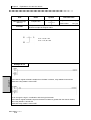
Thank you very much for purchasing TOYO FA Digital Controller ǴGPCsx.
This Programming Manual –Instruction word is to explain the way of thinking in
programming, relays and registers, and each instruction word. Read this Programming
Manual carefully to use the ǴGPCsx properly.
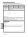
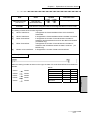
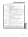
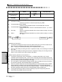
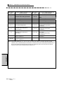
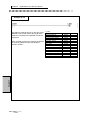
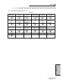
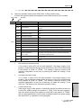
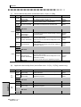
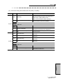
Also, read the relevant manuals given in the following table as well.
Description
Manual Number
Contents
ǴGPCsx Series Programming
Manual (Operation)
IGJ058A
ǴGPCsx Series Programming
Manual (Technique)
IGJ059A
Explanations of the menus, icons, etc. of
the TdsxEditor as well as of all the
operations of the TdsxEditor.
It explains how to configure and prepare
programs.
ǴGPCsx User’s Manual
(Hardware)
IGJ060A
It explains the system configuration,
specifications of hardware of each module,
etc. of the ǴGPCsx Series
Caution
(1)
(2)
(3)
Reprint and reproduction of this manual in part, or in its entirety are
prohibited.
Please note that the contents of this manual are subject to change
without prior notice for improvements.
Regarding the contents of this manual, we have tried to make them as
much complete as possible, but if you have noticed any ambiguities
and/or errors etc., please do not hesitate to contact our sales office
stated at the back of this manual. When you do so, please inform us of
the manual number indicated on the front cover.
1
Safety Notice
Read the “Safety Notice” carefully before using the product, and use it properly.
In this manual, matters that require attention for safety are divided into “Danger”
and “Caution”, which have the following meanings.
Danger
Caution
:
Mishandling may cause death or serious injury.
Mishandling may cause intermediate bodily injury, minor injury or damage
to property.
Note that the matter described with
Caution
may cause serious results
depending on the circumstances.
Each of the above describes important contents, which must strictly be observed.
Matters requiring special attention are given below, which are also indicated by the
above marks in the text of this manual.
Danger
•
Emergency stop circuit, interlock circuit etc. must be configured outside of the PC.
Failure to observe this may result in breakage in machines or accidents caused by a fault of the PC.
Caution
•
Change of a program, forced output, start, stop etc. while in operation must be made after making sure
that safety has been secured.
Failure to observe this may cause breakage in machines or an accident as a result of functioning of
machines by misoperation.
2
Revision History
*
Manual number is indicated at the right side of the
bottom of the cover sheet of this manual.
Printed date
* Manual number
Contents of revision
May, 2001
IGJ060A
Printing of the First Edition
(Temporary Edition)
3
Revision History
4
Table of Contents
Preface
Safety Notice
Revision History
Table of Contents
Chapter 1
Outline ............................................................................................1-1
Chapter 2 Programming Method Using the
Chapter 3
3-1
3-2
3-3
3-4
3-5
3-6
3-7
3-8
Chapter 4
4-1
4-2
4-3
Chapter 5
-GPC Language ..................2-1
Data Type and Range That Can Be Handled ...............................3-1
Kinds of Data .......................................................................................... 3-1
3-1-1
Logic Data................................................................................. 3-1
3-1-2
Numerical Data ......................................................................... 3-1
Kinds of Data Types ............................................................................... 3-2
3-2-1
Types of Logic Data .................................................................. 3-2
3-2-2
Types of Numerical Data........................................................... 3-2
16-bit integer type (i-form)....................................................................... 3-2
16-bit BCD type (u-form)......................................................................... 3-2
32-bit integer type (w-form)..................................................................... 3-3
32-bit BCD type (v-form) ......................................................................... 3-3
32-bit real number type (r-form) .............................................................. 3-4
Relation Between the Logic Data and the 16-Bit Integer Data
(i-Form)................................................................................................... 3-5
Kinds of Relays and Registers.....................................................4-1
Relation Between the Local Variable and Global Variable and the
Subprogram............................................................................................ 4-1
Number of Relays and Registers That Can Be Used .............................. 4-2
Outline of the Special Relay.................................................................... 4-6
Explanations of Instruction Words
Appendix
(Appendix 1)
(Appendix 2)
(Appendix 3)
(Appendix 4)
Symbols and each name ..............................................................A-1
Link data area inside the FL-net module .......................................A-4
System memory area..................................................................A-12
Error status related to the message function ...............................A-37
5
Chapter 1
Chapter 1 Outline
Chapter 1
Outline
Chapter 1
Chapter 1 Outline
Chapter 1 Outline
In the ǴGPCsx series, we have developed a new language for the ǴGPC as a
control language for application programs, without using computer languages (assembly
language, C-language, etc.).
The ǴGPC language employs the ladder network that has been conventionally
used in sequencers, etc. for logic operations, and D-F-S (data-flow-symbol) that has been
used in analog computers, etc. for numerical operations, and is a new programming
technique that enables the visual programming on programming tools that make use of
personal computers.
The ǴGPC language features the following.
(1) It has an optimum language system that has revolutionized the concept of computer
languages.
(It does not describe the processing procedure of a microprocessor, but describes
the processing procedure of data.)
(2) It is a graphic display language and makes a program very easy to understand,
thus enabling a programming with minimum errors.
(It is possible to program both logic operations and data processing on the same
screen.)
(3) Since it automatically converts the types of data handled (integer, BCD type, real
number, etc.), there is no need to use type conversion instructions in a program.
(If a data is used by dividing it, conversion instructions can be used.)
(4) Since abundant time series functions for control such as S-letter operation, etc. can
be utilized, a function that has been realized by means of multiple ladder symbols
can be described with 1 symbol, thus enabling anyone to create programs.
(Because it automatically adjusts the time spent for the execution of a program
while measuring it, you do not need to pay attention to the time at all.
(5) With it, you can make index decorations by means of 3 index registers (X, Y and Z),
and also can create flexible programs typical of computers.
(It also helps decrease the number of steps by means of a program loop using jump
instructions.)
(6) It enables you to prepare structured programs using subprograms with ease.
(It is best suited to the reuse and standardization of application programs.)
(7) With it, you can create 2 multi-task programs, thereby constructing an efficient
system.
(Since the execution cycle time can independently set, the execution cycle can be
divided into 2, a fast one and a slow one.)
(8) Because all the information regarding programs is stored in CPU main body, even if
the personal computer that was used at the time of development has been
damaged, you can maintain it by using another personal computer.
(Since the comments on programs can also be recovered, maintenance can be
carried out as a set of programs, comments and execution data.)
(9) By mean of a programming tool (TDsxEditor) that has a rich supply of convenient
functions, the changing work at the time of a system change can be carried out in a
very short time, with minimized errors and surely.
(For the details of loader, monitor, debugger, trend, trace back functions, etc. while
in the state of being RUN, refer to the TdsxEditor Operation Manual.)
1-1
Chapter 1
Chapter 1 Outline
Chapter 2
Programming Method Using the
-GPC Language
Chapter 2
Chapter 2 Programming Method Using the µ-GPC Language
Chapter 2
Chapter 2 Programming Method Using the µ-GPC Language
Chapter 2 Programming Method Using the µ-GPC Language
Chapter
Programming Method Using the
2
-GPC Language
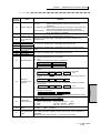
In the ǴGPCsx, programs loaded on 1 CPU is constructed using a concept of
project.
A project is given a name that can be changed freely. (You should determine the
most appropriate name.)
system definition, task 1, task 2 and
(1)
System definition
(2)
This is to define the hardware related conditions of CPU, consisting of 4 parts:
system configuration definition (I/O assignment), system operation definition, CPU
operation definition and redundancy definition.
Task 1, task 2
(3)
A task having higher priority is made to be task 1, which consists of scan time,
memory transfer definition, trace back setting and other multiple programs. Each
subprogram is given a program name (it shall be NoName if no designation is
made), which can be changed to any appropriate processing name, etc. that it
handles within a program.
1 subprogram should be written on a programming sheet comprising 12
horizontal columns and 19 vertical rows. 1 programming sheet is made to be 1
page, and pages can be added successively.
Within a subprogram, local symbols can be used, but a handing over between
subprograms can only be effected by the global memory.
Subroutine
(4)
It is a subroutine commonly used, in the same way as the subprograms in
task 1 and task 2.
The name of a subroutine (in 6 English alphanumeric codes) should be
determined and added.
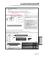
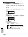
Programming sheet
Of the 12 horizontal columns, each column comprises a symbol insertion part
and a crosspoint part. By placing symbols in these parts and inputting label
names, a program is completed.
(There are not END instruction or compiling operation, with a compilation being
automatically made at the time of quitting the editor.)
In columns 1 - 11, the contact using the ladder symbols and data flow
symbols can be placed.
Column 12 is dedicated to a coil using the ladder symbols, and nothing can
be placed except a coil.
Also, there is no crosspoint in column 11, and therefore no intersection of
addition instructions or ladder symbols can be inserted.
Usually, 2-term operators (addition, subtraction, multiplication, etc) are placed
at a cross point, but as for the C-contact, since its contact name is input, it is to be
placed in the symbol insertion part.
2-1
Chapter 2
1 project can be divided into 4 parts:
subroutine.
Chapter 2 Programming Method Using the µ-GPC Language
Chapter 2
(5)
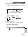
Of the 19 vertical rows, each row (line) comprises a label name part, a symbol
insertion part and a data comment part.
In a program that uses crosspoints, a programming is made over multiple
rows, but a program exceeding 19 lines shall be divided in multiple pages using a
temporary label.
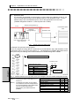
Program comment
In the programming sheet, column 13 can be used for comments as shown in
the programming example in the figure below, and if a coil is placed with a ladder
symbol, it is reflected to the position of comment at the applicable contact point. (It
is automatically displayed, unless it is input at the contact side.)
Note, however, that the maximum characters that can be input are three
2-byte characters (six 1-byte characters), and hence consider a character string
that is best suited to your identification of it.
Also, as in the first line, the position for comments bearing no symbols can be
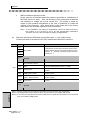
used for comments in its entirety.
This program is an example of solution to an
exercise problem for training.
Problem 1
Operation
Stop
Lamp
When ON
ON time
When OFF
OFF time
When ON When OFF
Problem 2
Problem 3
Problem 4, 5
2-2
Chapter 2 Programming Method Using the µ-GPC Language
Explanations on the sample program
For your reference, explanations are given of the example of programming for
the exercise problem for training mentioned above.
The 1st line is a comment line. As shown in this example, the contents of
the program, etc. should be described beforehand.
The 2nd line is a blank line. It is inserted, where necessary, to make the
program list easier to read.
The 3rd - 4th lines are ladder symbols of a HOLD circuit that uses a typical
2-operation switch.
By turning the input switch I00000 ON, the lamp circuit O00020 is turned on to
light up, and the status is kept on HOLD.
I00001 is a B-contact input switch to release the above HOLD. If it is ON, the
above lamp is turned off.
The 5th line is a blank line.
The 6th - 9th lines are a flash circuit of a lamp in which an on-delay timer and
an off-delay timer are combined.
Each of the on-time and off-time can
independently be changed.
The setting time of each timer should be specified at the lower side of the coil
in column 12 for time setting. In the example above it is set at 1.0 S (second), but
the setting can be made up to 2 hours, representing the hour by H, the minute by M,
and the second by S. The minimum unit is 10 mS, which should be written as 0.01
S.
The 10th line is a blank line.
The 11th - 12th lines are a circuit to read a numerical data from the 16-bit
input module, add a constant 123 to it, divide the added value by 60 to obtain a
remainder, and turn the lamp on if the remainder exceeds 30.
Since the results of operations in the process are stored in registers, when
debugging you can monitor the result while checking these. At the right side of the
comparison instruction symbol comes the logic operation symbol.
The 13th line is a blank line.
The 14th - 19th lines show an example of a pattern generation circuit that
uses a latch relay and a change ratio limitation function (we call it ARC). It
generates triangular waves continuously. The wave height value can be set from
the input module using numerical values of BCD type. The cycle can be changed
indirectly by changing the alteration ratio parameters of the ARC function. In the
18th line and the 19th line, real number operation, integer operation and BCD
operation are mingled, and the patterns are continuously generated by switching
the input value of ARC by means of the C-contact.
The C-contact at B0000F is for test use, and it directly output the input value
by turning it on using a debugger.
2-3
Chapter 2
(6)
Chapter 3 Data Type and Range That Can Be Handled
Chapter 3
Data Type and Range That Can Be
Handled
3-1-1
3-1-2
Logic Data .............................................................................................. 3-1
Numerical Data....................................................................................... 3-1
3-2 Kinds of Data Types .................................................................................3-2
3-2-1
3-2-2
Types of Logic Data................................................................................ 3-2
Types of Numerical Data ........................................................................ 3-2
3-3 16-bit integer type (i-form)........................................................................3-2
3-4 16-bit BCD type (u-form)...........................................................................3-2
3-5 32-bit integer type (w-form)......................................................................3-3
3-6 32-bit BCD type (v-form)...........................................................................3-3
3-7 32-bit real number type (r-form)...............................................................3-4
3-8 Relation Between the Logic Data and the 16-Bit Integer Data
(i-Form) ......................................................................................................3-5
Chapter 3
3-1 Kinds of Data.............................................................................................3-1
Chapter 3
Chapter 3 Data Type and Range That Can Be Handled
Chapter 3 Data Type and Range That Can Be Handled
Chapter 3 Data Type and Range That Can Be Handled
The data handled in the ǴGPCsx is represented by a label name of 2-digit type
plus 4-digit hexadecimal number.
Also, the foremost 1 digit of the hexadecimal number can be replaced by the index
label X, Y, Z.
Examples of a label: IOX123 b0y234 mr02AF
3-1 Kinds of Data
The data handled in the ǴGPCsx can roughly be divided into 2 kinds: “logic
data” and “numerical data”.
•
Logic data is a data that represents logic of 1 bit, namely “1” or “0”.
•
Logic data is processed by logic operations, etc.
•
Logic data is stored in a “relay”, and it can be referred to in a program by
designating a “relay number”.
•
The result of operation of the comparison operation symbol is a logic data.
Points
•
In the ǴGPCsx, that which stores logic data is called a “relay”.
•
“1” in logic data corresponds to the state of “ON” of a relay, and “0” in logic
data corresponds to the state of “OFF” of a relay.
3-1-2Numerical Data
•
Numerical data is a data that represents 16 bits (1 word) or 32 bits (2 words)
as 1 unit.
•
Numerical data is stored in a “register”, and it can be referred to in a program
by designating a “register number”.
•
The input condition of the comparison operation symbol is a logic data.
Point
•
In the ǴGPCsx, that which stores numerical data is called a “register”.
An uppercase character should be used as the initial letter of the relay number of a
logic data.
(e.g)
I00000
A lowercase character should be used as the initial letter of the register number of a
numerical data.
(e.g)
i00000
3-1
Chapter 3
3-1-1Logic Data
Chapter 3 Data Type and Range That Can Be Handled
3-2 Kinds of Data Types
3-2-1Types of Logic Data
There is no particular distinction of types.
The data that can be handled is 1 (ON) or 0 (OFF).
3-2-2Types of Numerical Data
Chapter 3
There are the following 5 kinds, which will be explained in 3-3 and thereafter.
[1]
16-bit integer type (i-form)
[2]
16-bit BCD type (u-form)
[3]
32-bit integer type (w-form)
[4]
32-bit BCD type (v-form)
[5]
32-bit real number type (r-form)
3-3 16-bit integer type (i-form)
It represents a 16-bit integer value signed data as 1 unit (1 word).
The range of data that is handled internally is:
-32,768 - 32,767 (8000H - 7FFFH)
Such a numerical data is called a “16-bit integer data”.
3-4 16-bit BCD type (u-form)
It represents a 16-bit BCD (binary coded decimal) data of 4-digit as 1 unit (1 word).
The range of data that is handled internally is:
0000 - 9999 (0000H - 270FH)
Such a numerical data is called a “16-bit BCD data”.
Note:
3-2
The 16-bit BCD data can only be used with regard to a data exchanged
with an input and output (I/O) unit (I/O data).
Chapter 3 Data Type and Range That Can Be Handled
3-5 32-bit integer type (w-form)
It represents a 32-bit integer value signed data as 1 unit (2 words occupied).
The range of data that is handled internally is:
-2147483648 - 2147483647 (80000000H - 7FFFFFFFH)
Such a numerical data is called a “32-bit integer data”.
Note:
The 32-bit integer data can only be used with regard to a data exchanged
with an input and output (I/O) unit (I/O data).
3-6 32-bit BCD type (v-form)
It represents a 32-bit BCD (binary coded decimal) data of 8-digit as 1 unit
(2 words occupied).
The range of data that is handled internally is:
Chapter 3
00000000 - 99999999 (00000000H - 05F5E0FFH)
Such a numerical data is called a “32-bit BCD data”.
Note:
The 32-bit BCD data can only be used with regard to a data exchanged
with an input and output (I/O) unit (I/O data).
3-3
Chapter 3 Data Type and Range That Can Be Handled
3-7 32-bit real number type (r-form)
It represents a 32-bit floating-point format data as 1 unit (2 words occupied).
The range of data that is handled internally is:
-6.2573187 × 1038 - 6.2573187 × 1038
Such a numerical data is called a “32-bit real number data”.
For reference:
The 32-bit real number data is handled internally as follows.
(There is no need for a user to pay attention to it.)
(-1)S × 2e-127 × 1.f
s: value of the sign part
e: value of the exponent part
Chapter 3
f: value of the mantissa part (normalized to a 23-bit binary number)
31
3-4
30
23
22
0
S
exponent part
mantissa part
1-bit
8-bit
23-bit
Chapter 3 Data Type and Range That Can Be Handled
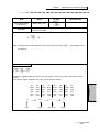
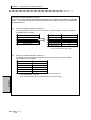
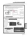
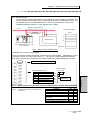
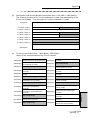
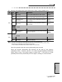
3-8 Relation Between the Logic Data and the 16-Bit Integer Data (i-Form)
The “logic data” handled in the ǴGPCsx can be put together into a group of
16 bits that is put in correspondence with one “16-bit integer (i-form) data”.
In this case, there are the following relations among the logic data and 16-bit
integer data, and the relay and register that store these data, and the relay number
and register number.
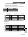
(Example) Continuous relay numbers I00120, I00121, - I0012F are in
correspondence with the input relays that contain 16 pieces of logic
data. Meanwhile, register number i00012 is in correspondence with
the input register that contains 1 piece of 16-bit integer data. The
relation between both of these can be illustrated as Fig. 3.1.
This figure represents how the content of input register i00012: 5AA5
(hexadecimal) is developed in input registers I00120, I00121, - I0012F.
I 00121
0
I 00122
1
I 00123
0
I 00124
0
I 00125
1
I 00126
0
I 00127
1
I 00128
0
I 00129
1
I 0012A
0
I 0012B
1
I 0012C
1
I 0012D
0
I 0012E
1
I 0012F
0
Chapter 3
Input relay
number Value
I 00120
1
Input register bit
number
i00012
F E D C
0 1 0 1
B A 9 8
1 0 1 0
7 6 5 4
1 0 1 0
3 2 1 0
0 1 0 1
Input register
5
A
A
5
h
3-5
Chapter 3 Data Type and Range That Can Be Handled
Likewise, the relation of correspondence between the input relays that are put
into a group of 16 bit and the input register is as follows.
Input relay number
I00000, I00001, -, I0000F
I00010, I00011, -, I0001F
I00020, I00021, -, I0002F
Input register bit number
i00000
i00001
i00002
Aside from these, each kind of relays such as output relays, link relays,
auxiliary relays, etc. can likewise be put in correspondence with the output register,
link register, auxiliary register, etc.
Point:
Relation of correspondence between the relay number and the register
number
Chapter 3
(Example)
Relay number I00123 represents bit number 3 of register number i00012.
Note:
The range of relay numbers and register numbers depends on the kinds of
relays and registers.
Some registers will make no sense when developed in relays, and hence
they cannot be developed (kr, mr, mi, etc.)
3-6
Chapter 4 Kinds of Relays and Registers
Chapter 4
Kinds of Relays and Registers
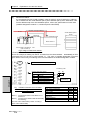
4-1 Relation Between the Local Variable and Global Variable and the
Subprogram...............................................................................................4-1
4-2 Number of Relays and Registers That Can Be Used .............................4-2
Chapter 4
4-3 Outline of the Special Relay.....................................................................4-6
Chapter 4
Chapter 4 Kinds of Relays and Registers
Chapter 4 Kinds of Relays and Registers
Chapter 4 Kinds of Relays and Registers
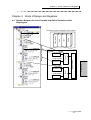
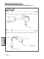
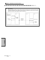
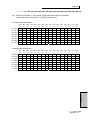
4-1 Relation Between the Local Variable and Global Variable and the
Subprogram
Output
Input
CPU
Power supply
Example of system configuration of the µGPCsx
Local variable
No Name 2
Local variable
Local variable
Task 2
No Name 3
No Name 4
4-1
Chapter 4
Global variable
Local variable
Task 1
No Name 1
Chapter 4 Kinds of Relays and Registers
•
Local variable ---- A variable that can be referred to within 1 subprogram only
(it cannot be referred to from other subprograms).
The number used should be set by the “number of relays
and registers” in each subprogram.
It should be prepared by dividing it depending on the
processing function.
(Example)
•
mi, B0, etc.
Global variable -- A variable that can be referred to from any subprogram
within 1 project.
The number used should be set by the parameters of CPU
in the “system configuration definition”.
(Example) G0, fi, RI, etc.
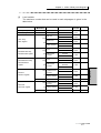
4-2 Number of Relays and Registers That Can Be Used
[1]
Global variable
The maximum number of variables that can be used in any POU (program)
within a project is given in the table below.
Name
Chapter 4
Input relay
Input register
Number used
(Maximum)
8,192
512
Kind
Data number
Contact
Input data
I00000 - I01FFF
i0000 - i01FF
Output relay
(8,192)
Coil, contact
O00000 - O01FFF
Output register
Announcing relay
Announcing register
(512)
32,768
Output data
o0000 - o01FF
Z00000 - Z07FFF
Global relay
Global register
2,048
System
information
131,072
Coil, contact
8,192
4,096
65,536
Retain relay
Retain register
Network relay
Network register
Global data
Coil, contact
4,096
2,048
65,536
4,096
2,048
z00000 - z007FF
G00000 - G1FFFF
g00000 - g01FFF
gr0000 - gr1FFE
Coil, contact
Network data
Load
*1
*3
Store
*1
*3
Load
Load
Store
*2
RI0000 - RIFFFF
ri0000 - ri0FFF
Retain data
Data
Remarks
direction
rr0000 - rr0FFF
FI0000 - FIFFFF
fi0000 - fi0FFF
fr0000 - fr0FFE
Load
Store
Load
Store
*2
*2
*1: The number used should be a total number of inputs and outputs.
*2: No odd number can be used.
*3: In the , u (BCD 4-digit), v (BCD 8-digit) or w (32-bit integer) is to be indicated, which represents
the type of an I/O register.
4-2
Chapter 4 Kinds of Relays and Registers
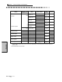
[2]
Local variable
The maximum number that can be used in each subprogram is given in the
table below.
Auxiliary relay
Auxiliary register
Number used
(Maximum)
512
32
Kind
Coil, contact
Auxiliary data
Set coil
Latch relay
Latch register
512
Reset coil
32
Latch contact
ON differential relay
ON differential register
OFF differential relay
OFF differential
register
ON timer
ON timer register
OFF timer
OFF timer register
512
32
512
32
Coil
Differential
contact
Coil
Differential
contact
224
Coil,
instantaneous
contact
14
Timing contact
Data
Remarks
direction
B00000 - B001FF
Load
Store
b00000 - b0001F
Data number
LS0000 - LS01FF
ls0000 - ls001F
LR0000 - LR01FF
lr0000 - lr001F
LC0000 - LC01FF
Load
Store
Load
Store
Load
lc0000 - lc001F
US0000 - US01FF
us0000 - us001F
UC0000 UC01FF
Load
Store
Load
uc0000 - uc001F
DS0000 - DS01FF
ds0000 - ds001F
Load
Store
DC0000 DC01FF
Load
ds0000 - ds001F
TS0000 - TS00DF
ts0000 - ts0009
TD0000 - TD00DF
td0000 - td0009
Load
Store
Load
224
Lapse of time
tn0000 - tn00DF
Load
224
Coil,
instantaneous
contact
TR0000 - TR00DF
Load
Store
14
Timing contact
224
Lapse of time
tr0000 - tr0009
TC0000 - TC00DF
tc0000 - tc0009
tf0000 - tf00DF
Chapter 4
Name
Load
Load
4-3
Chapter 4 Kinds of Relays and Registers
Name
Counter
Number used
(Maximum)
192
Kind
Reset coil
Preset coil
UP coil
DOWN coil
12
Counter register
Operation data
Constant data
Pattern data
Stack register
Chapter 4
Index register
Zero detection
contact
192
Present value
of the count
Data number
NR0000 - NR00BF
nr0000 - nr000B
NP0000 - NP00BF
np0000 - np000B
NU0000 - NU00BF
nu0000 - nu000B
ND0000 - ND00BF
nd0000 - nd000B
NZ0000 - NZ00BF
nz0000 - nz000B
512
Integer
N00000 - n000BF
mi0000 - mi01FF
256
Real number
mr0000 - mr00FF
512
Integer
ki0000 - ki01FF
256
Real number
kr0000 - kr00FF
10
Integer
pi0000 - pi0009
10
Real number
pr0000 - pr0009
Data
Remarks
direction
Load
Store
Load
Store
Load
Store
Load
Store
Load
Load
Load
Store
Load
Load
256
Integer
si0000 - si00FF
128
Real number
sr0000 - sr007F
Load
Store
Integer
indx_x, indx_y,
indx_z
Load
Store
3
*1
*1
*2
*1: The number of patters that can be used varies depending on the setting of the number of points of
pattern data.
*2: No odd number can be used.
4-4
Chapter 4 Kinds of Relays and Registers
Shared structure of registers
The global register and stack register are in the relation of a shared
body to realize the ease of handling.
The relation of a shared body between the relays, integer registers and
real number registers of the global memory is given in the table below.
Among them, sr0000 represents a live line data, and sr0002 represents
the first argument.
Relay name
Integer
register
Real number
register
G00000
Relay name
Integer
register
Real number
register
SI0000
G00001
G00002
g00000
Si0000
G0000F
sr0000
gr0000
G00010
G00011
G00012
g00001
Chapter 4
(3)
G0001F
G00020
SI0020
Si0002
g00002
G0002F
gr0002
g00030
sr0002
g00003
G0003F
Note: Since the relation of a shared body allows an operation from any register, special
attention should be paid when using it.
4-5
Chapter 4 Kinds of Relays and Registers
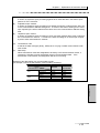
4-3 Outline of the Special Relay
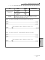
[1]
latch relay/register
B00000
B00001
LS0000
LR0000
LC0000
B00002
Chapter 4
When set coil LS0000 is turned ON, latch contact LC0000 is turned ON, and
000020 is kept turned ON.
When reset coil LR0000 is turned ON, latch contact LC0000 is turned OFF,
and 000020 is kept turned OFF.
The latch contact LC0000 delay for 1 scan from latch coil.
The latch coil is usually turned OFF when power supply is made open.
If you wish to retain the latch coil even when power supply is open, use the
retain memory to transfer by means of the memory transfer definition, or use SET
RESET functions (set the retain relay as a parameter).
(Memory transfer definition: before operation)
(Memory transfer definition: after operation)
RI0000 → LC0000
LC0000 → RI0000
In order to realize the same functions within the subroutine, use SET RESET
functions by means of SI0000 in the subroutine.
4-6
Chapter 4 Kinds of Relays and Registers
ON/OFF differential relay/register
B00010
US0000
UC0000
B00011
B00020
Chapter 4
(2)
DS0000
DC0000
B00021
When coil US0000 is turned ON, after a delay for 1 scan, differential contact
UC0000 is turned ON for 1 scan.
When coil DS0000 is turned OFF, after a delay for 1 scan, differential contact
DC0000 is turned ON for 1 scan.
Aside from these, there are USUC function and DSDC function to realize the
same functions.
4-7
Chapter 4 Kinds of Relays and Registers
[3]
ON/OFF timer relay/register
B00050
TS0000
TD0000
B00051
B00060
TR0000
Chapter 4
TC0000
B00061
When coil TS0000 is turned ON, after the set time has lapsed, timing contact
TD0000 is turned ON. TD0000 is turned OFF within 1 scan after TS0000 has
been turned OFF.
(The timer setting value should be input at the lower side of the TS coil.)
Where, S stands for second, M for minute and H for hour, and the setting can
be made from 0.01 seconds to 2 hours.
When coil TR0000 is turned ON, timing contact TD0000 is turned ON within 1
scan after TR0000 has been turned ON. TD0000 is turned OFF after the set time
has lapsed.
(The timer setting value should be input at the lower side of the TR coil.)
Where, S stands for second, M for minute and H for hour, and the setting can
be made from 0.01 seconds to 2 hours.
4-8
Chapter 4 Kinds of Relays and Registers
Counter relay/register
n00000
Chapter 4
[4]
NR0000
NP0000
NU0000
ND0000
NZ0000
The initial value of the counter is 0. Next, the up coil is turned ON, and the
counter value is increased by 1. Also, the zero detection contact is turned ON at 0
initially, but since 1 has been added, it is not 0, so it is turned OFF.
And in addition, the up coil is turned ON, and the counter value is increased
by 1 to become 2.
The preset coil is turned ON, and the counter value becomes 15.
The preset value should be set at the lower side of the NP coil.
The down coil is turned ON, and the counter value is decreased by 1.
The reset coil is turned ON, and the counter value becomes 0, and the zero
detection contact is turned ON.
4-9
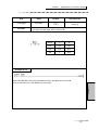
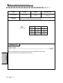
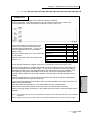
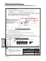
Chapter 5 Explanations of Instruction Words
Chapter 5
Chapter 5
Explanations of Instruction Words
Chapter 5
Chapter 5 Explanations of Instruction Words
Chapter 5 Explanations of Instruction Words
Chapter 5 Explanations of Instruction Words
How to read the table
It shows each
Note)
symbol drawing
It shows the name
of each symbol.
It is classified for
the operation of
each symbol.
Kind
Name
Symbol
Execution
time
Function
It shows the
execution time of
each symbol.
It shows the
function of each
symbol.
Example of
use
It shows an example of use or a trend
graph within the actual circuit.
Relay and Reg that are displayed in the symbol column hereafter are explained herein.
The figure on the left shows a relay. Herein it is represented by the
word RELAY for simplification. All the relays such as G0, I0, B0, etc.
can be set to RELAY.
The figure on the left shows a register. Herein it is represented by
the word REG for simplification. All the registers such as g0, mi, kr,
etc. can be set to REG.
5-1
Chapter 5
Note)
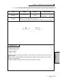
Chapter 5 Explanations of Instruction Words
Kind
Name
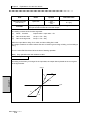
LD language
A-contact
Function
Symbol
Execution time
0.02 [µs]
If RELAY is ON, the input logic value is output.
If it is OFF, the output logic value is turned OFF.
RELAY
A
B
ON
ON
ON
ON
OFF
OFF
OFF
X
OFF
X: don’t care
Example of use
Chapter 5
When both of relay B00000 and relay B00001 are ON, relay B00010 is turned ON.
In other cases than this, relay B00010 is turned OFF.
5-2
Chapter 5 Explanations of Instruction Words
Kind
Name
LD language
B-contact
Function
Symbol
Execution time
0.02 [µs]
If RELAY is OFF, the input logic value is output.
If it is ON, the output logic value is turned OFF.
RELAY
A
B
OFF
ON
ON
OFF
OFF
OFF
ON
X
OFF
X: don’t care
Example of use
Chapter 5
When relay B00000 is ON and relay B00001 is OFF, relay B00010 is turned ON.
In other cases than this, relay B00010 is turned OFF.
5-3
Chapter 5 Explanations of Instruction Words
Kind
Name
LD language
B-contact
Function
Symbol
Execution time
0.02 [µs]
If RELAY is OFF, the input logic value is output.
If it is ON, the output logic value is turned OFF.
RELAY
A
B
OFF
ON
ON
OFF
OFF
OFF
ON
X
OFF
X: don’t care
Example of use
Chapter 5
When relay B00000 is ON and relay B00001 is OFF, relay B00010 is turned ON.
In other cases than this, relay B00010 is turned OFF.
5-4
Chapter 5 Explanations of Instruction Words
Kind
Name
LD language
Coil
Function
Symbol
Execution time
0.10 [µs]
It outputs the input logic value to RELAY.
A
RELAY
ON
ON
OFF
OFF
Example of use
Chapter 5
When relay I00000 is ON, both relay 000020 = 0N and relay B00000 are turned ON.
When relay I00000 is OFF, both relay 000020 and relay B00000 are turned OFF.
5-5
Chapter 5 Explanations of Instruction Words
Kind
Data flow language
(Basics)
Function
Name
Symbol
Execution time
Load
Integer
0.48 [µs]
Store
Real number
0.45 [µs]
Load: The data in REG is made to be the output numerical value.
Store: The input numerical value is output to REG.
D1 = REG
REG = D2
Chapter 5
Example of use
The data in register ki0000 (2) is loaded and stored in register mi0000.
Next, the data in register mi0000 is loaded and stored in register mr0000.
Since register mr0000 is a register of the real number type, type conversion from an integer to a
real number is carried out and a data (2.0) is stored.
5-6
Chapter 5 Explanations of Instruction Words
Kind
Name
Data flow language
(Basics)
Store & load store
Function
Symbol
Execution time
Integer
Real number
0.48 [µs]
0.45 [µs]
The input numerical value is output to REG, and the data of REG is
made to be the output numerical value.
It is used when data in the midst of operation should be retained in REG.
REG = D1
D2 = REG
The data in register mi0000 and the data in register mi0001 are added and the result is stored in
register mi0002.
Next, the data in register mi0003 is subtracted from the data in register mi0002 and the result is
stored in register mi0004.
In register mi0002, the addition data in the midst of operation is stored.
5-7
Chapter 5
Example of use
Chapter 5 Explanations of Instruction Words
Kind
Name
Data flow language
(Basics)
Addition
Function
Symbol
Execution time
Integer
1.15 [µs]
Real number
1.13 [µs]
Two input numerical values are added and the result is output.
The operation can be made even if their types are different. However,
an integer is converted to a real number, which is then subjected to the
real number operation.
D3 = D1 + D2
On type conversion
If the type of the register being used in 1 operation block is the integer type or the 16-bit BCD type,
the data are converted to the 16-bit integer type before subjected to operation, whereas if a
register of the real number type, 32-bit integer type or 32-bit BCD type is used, it is converted to
the real number type before subjected to operation.
(After this, type conversion is also carried out for subtraction, multiplication, division, remainder,
priority given to a higher-level, and priority given to a lower-level.)
Chapter 5
Example of use
The data in register mi0000 and the data in register mr0000 are added and the result is stored in
register mr0001.
Although the data in register mi0000 is an integer, since the data in register mr0000 is a real
number, addition is made after type conversion of integer/real number has been made.
5-8
Chapter 5 Explanations of Instruction Words
Kind
Name
Data flow language
(Basics)
Subtraction
Function
Symbol
Execution time
Integer
Real number
1.27 [µs]
1.25 [µs]
Subtraction is made with two input numerical values and the result is
output.
Operation can be carried out even if the types are different. However,
an integer is converted to a real number, which is then subjected to the
real number operation.
D3 = D1 - D2
The data in register mr0000 is subtracted from the data in register mi0000 and the result is stored
in register mr0001.
Although the data in register mi0000 is an integer, since the data in register mr0000 is a real
number, subtraction is made after type conversion of integer/real number has been made.
5-9
Chapter 5
Example of use
Chapter 5 Explanations of Instruction Words
Kind
Name
Data flow language
(Basics)
Multiplication
Function
Symbol
Execution time
Integer
1.17 [µs]
Real number
1.13 [µs]
Two input numerical values are multiplied and the result is output.
Operation can be carried out even if the types are different. However,
an integer is converted to a real number, which is then subjected to the
real number operation.
D3 = D1 * D2
Chapter 5
Example of use
Multiplication of the data in register mi0000 and the data in register mr0000 is performed and the
result is stored in register mr0001.
Although the data in register mi0000 is an integer, since the data in register mr0000 is a real
number, multiplication is made after type conversion of integer/real number has been made.
5-10
Chapter 5 Explanations of Instruction Words
Kind
Name
Data flow language
(Basics)
Division
Function
Symbol
Execution time
Integer
Real number
2.48 [µs]
2.32 [µs]
Division of two input numerical values is performed and the result is
output.
Operation can be carried out even if the types are different. However,
an integer is converted to a real number, which is then subjected to the
real number operation.
D3 = D1 / D2
Division of the data in register mi0000 and the data in register mr0000 is performed and the result
is stored in register mr0001.
Although the data in register mi0000 is an integer, since the data in register mr0000 is a real
number, division is made after type conversion of integer/real number has been made.
5-11
Chapter 5
Example of use
Chapter 5 Explanations of Instruction Words
Kind
Name
Data flow language
(Basics)
Remainder
Function
Symbol
Execution time
2.48 [µs]
Division of two input numerical values is performed and the result
(remainder) is output.
D3 = D1 % D2
Note) Only operation with integers is valid.
Chapter 5
Example of use
The data in register mi0000 is divided by the data in register mi0001 and the result (remainder) is
stored in register mi0002.
5-12
Chapter 5 Explanations of Instruction Words
Kind
Name
Data flow language
(Basics)
Priority given to a
higher-level
Function
Symbol
Execution time
Integer
Real number
1.52 [µs]
1.45 [µs]
Two input numerical values are compared and a larger numerical value is
output.
Operation can be carried out even if the types are different. However,
an integer is converted to a real number, which is then subjected to the
real number operation.
If D1 > D2, D3 = D1
If D1 ≤ D2, D3 = D2
The data in register mi0000 and the data in register kr0000, 100.0 is compared and a larger data is
stored in register mr0001.
Although the data in register mi0000 is an integer, since the data in register kr0000 is a real
number, comparison is made after type conversion of integer/real number has been made.
It serves as a limiter of which lower limt value is the data in register kr0000 (100.0).
5-13
Chapter 5
Example of use
Chapter 5 Explanations of Instruction Words
Kind
Name
Data flow language
(Basics)
Priority given to a
lower-level
Function
Symbol
Execution time
Integer
1.43 [µs]
Real number
1.64 [µs]
Two input numerical values are compared and a smaller numerical value
is output.
Operation can be carried out even if the types are different. However,
an integer is converted to a real number, which is then subjected to the
real number operation.
If D1 > D2, D3 = D2
If D1 ≤ D2, D3 = D1
Chapter 5
Example of use
The data in register mi0000 and the data in register kr0000, 100.0 is compared and a smaller data
is stored in register mr0001.
Although the data in register mi0000 is an integer, since the data in register kr0000 is a real
number, comparison is made after type conversion of integer/real number has been made.
It serves as a limiter of which upper limit value is the data in register kr0000 (100.0).
5-14
Chapter 5 Explanations of Instruction Words
Kind
Name
Symbol
Data flow language
(Basics)
Product of numerical
values
Execution time
1.15 [µs]
Logical multiplication operation of two input numerical values is
performed and the result is output.
Function
D3 = D1 & D2
Note) Only operation with integers is valid.
Logical multiplication operation of the data in register mi0000 and the data in register ki0001 (3) is
performed and the result is stored in register mi0001.
If the data in register mi0000 is (10), then (2) is stored in register mi0001.
mi0000
ki0000
0000
0000
0000
0000
0000
0000
1010
0011
(10)
(3)
mi0001
0000
0000
0000
0000
(2)
5-15
Chapter 5
Example of use
Chapter 5 Explanations of Instruction Words
Kind
Name
Symbol
Data flow language
(Basics)
Sum of numerical
values
Execution time
1.15 [µs]
Logical sum operation of two input numerical values is performed and the
result is output.
Function
D3 = D1 | D2
Note) Only operation with integers is valid.
Chapter 5
Example of use
Logical sum operation of the data in register mi0000 and the data in register ki0001 (3) is
performed and the result is stored in register mi0001.
If the data in register mi0000 is (10), then (11) is stored in register mi0001.
5-16
mi0000
ki0000
0000
0000
0000
0000
0000
0000
1010
0011
(10)
(3)
mi0001
0000
0000
0000
1011
(11)
Chapter 5 Explanations of Instruction Words
Kind
Name
Symbol
Data flow language
(Basics)
Exclusive OR of
numerical values
Execution time
1.15 [µs]
Exclusive OR operation of two input numerical values is performed and
the result is output.
Function
D3 = D1 ^ D2
Note) Only operation with integers is valid.
Example of use
mi0000
ki0000
0000
0000
0000
0000
0000
0000
1010
0011
(10)
(3)
mi0001
0000
0000
0000
1001
(9)
Chapter 5
Exclusive OR operation of the data in register mi0000 and the data in register ki0001 (3) is
performed and the result is stored in register mi0001.
If the data in register mi0000 is (10), then (9) is stored in register mi0001.
5-17
Chapter 5 Explanations of Instruction Words
Kind
Name
Data flow language
(Basics)
a-contact
Function
Symbol
Execution time
Integer
1.52 [µs]
Real number
1.33 [µs]
If RELAY is ON, the input numerical value is output.
If it is OFF, the output numerical value is made to be 0.
If RELAY = ON, D2 = D1
If RELAY = OFF, D2 = 0
Example of use
Chapter 5
When relay I00000 is ON, the data in register mi0000 is stored in register mi0001.
When relay I00000 is OFF, (0) is stored in register mi0001.
5-18
Chapter 5 Explanations of Instruction Words
Kind
Name
Data flow language
(Basics)
b-contact
Function
Symbol
Execution time
Integer
Real number
1.52 [µs]
1.33 [µs]
If RELAY is OFF, the input numerical value is output.
If it is ON, the output numerical value is made to be 0.
If RELAY = ON, D2 = 0
If RELAY = OFF, D2 = D1
Example of use
Chapter 5
When relay I00000 is OFF, the data in register mi0000 is stored in register mi0001.
When relay I00000 is ON, (0) is stored in register mi0001.
5-19
Chapter 5 Explanations of Instruction Words
Kind
Name
Data flow language
(Basics)
c-contact
Function
Symbol
Execution time
Integer
Real number
1.15 [µs]
Depending on the logical value of RELAY, either of the two input
numerical values is selected and output.
If RELAY = ON, D3 = D1
If RELAY = OFF, D3 = D2
If RELAY = ON, D3 = D2
If RELAY = OFF, D3 = D1
Chapter 5
Example of use
When relay I00000 is OFF, the data in register mi0001 is stored in register mi0002.
When relay I00000 is ON, the data in register mi0000 is stored in register mi0002.
When relay I00000 is OFF, the data in register ki0000 (3) is stored in register mi0003.
When relay I00000 is ON, the data in register ki0001 (6) is stored in register mi0003.
5-20
1.31 [µs]
Chapter 5 Explanations of Instruction Words
Kind
Name
Data flow language
(Basics)
Compare high
Function
Symbol
Execution time
Integer
Real number
1.17 [µs]
1.21 [µs]
Comparison of two input numerical values is performed and the result of
decision is output as a logical value.
If D1 > D2, B = ON
If D1 ≤ D2, B = OFF
If the data in register mi0000 is greater than the data in mi0001, relay 000020 is turned ON.
Otherwise relay 00020 is turned OFF.
It can change the logic in combination with the logical reversal.
If the data in register mi0002 is equal to the data in mi0003 or smaller than the data in mi0003,
then relay 000021 is turned ON.
Otherwise relay 00020 is turned OFF.
5-21
Chapter 5
Example of use
Chapter 5 Explanations of Instruction Words
Kind
Name
Data flow language
(Basics)
Compare low
Function
Symbol
Execution time
Integer
1.17 [µs]
Real number
1.21 [µs]
Comparison of two input numerical values is performed and the result of
decision is output as a logical value.
If D1 < D2, B = ON
If D1 >= D2, B = OFF
Chapter 5
Example of use
If the data in register mi0000 is smaller than the data in mi0001, relay 000020 is turned ON.
Otherwise relay 00020 is turned OFF.
It can change the logic in combination with the logical reversal.
If the data in register mi0002 is equal to the data in mi0003 or greater than the data in mi0003,
then relay 000021 is turned ON.
Otherwise relay 00020 is turned OFF.
5-22
Chapter 5 Explanations of Instruction Words
Kind
Name
Data flow language
(Basics)
Compare equal
Function
Symbol
Execution time
Integer
Real number
1.17 [µs]
1.21 [µs]
Comparison of two input numerical values is performed and the result of
decision is output as a logical value.
If D1 = D2, B = ON
If D1 ≠ D2, B = OFF
Note)
If a real number is in the register used, then in some cases the result may not be turned
ON due to the minute numerical value that is not displayed.
If the data in register mi0000 is equal to the data in mi0001, then relay 000020 is turned ON.
Otherwise relay 00020 is turned OFF.
It can change the logic in combination with the logical reversal.
If the data in register mi0002 is not equal to the data in mi0003, then relay 000021 is turned ON.
Otherwise relay 00021 is turned OFF.
5-23
Chapter 5
Example of use
Chapter 5 Explanations of Instruction Words
Kind
Name
Data flow language
(Basics)
Load local constant
(integer, real number)
Function
Symbol
Execution time
Integer
0.91 [µs]
Real number
0.85 [µs]
It loads a local constant (integer, real number).
The constant is secured within the program (instead of the parameter).
The load local constant (integer) can be used within the operation block of i-form only.
(Integer) and (real number) cannot mingle within 1 operation block.
Chapter 5
Example of use
In register mi0000, the integer value (10) is loaded.
In register mr0000, the real number value (5.0000) is loaded.
5-24
Chapter 5 Explanations of Instruction Words
Kind
Name
Data flow language
(Function 1)
Code conversion
Function
Symbol
Execution time
Integer
Real number
0.38 [µs]
0.15 [µs]
Reversal of the positive/negative sign of input numerical values is
performed and output.
D2 = - (D1)
Example of use
Chapter 5
The sign of the data in register ki0000 (-10) is converted to positive and (10) is stored in register
mi0000.
The sign of the data in register kr0000 (5.0000) is converted to negative and (-5.0000) is stored in
register mr0000.
5-25
Chapter 5 Explanations of Instruction Words
Kind
Name
Data flow language
(Function 1)
Absolute value
conversion
Function
Symbol
Execution time
Integer
0.40 [µs]
Real number
0.15 [µs]
It obtains the absolute value of the input numerical value and output it.
If D1 < 0, D2 = - (D1)
If D1 >= 0, D2 = D1
Example of use
Chapter 5
Absolute value conversion is performed to the data in register ki0000 (10) and (10) is stored in
register mi0000.
Absolute value conversion is performed to the data in register kr0000 (-5.0000) and (5.0000) is
stored in register mr0000.
5-26
Chapter 5 Explanations of Instruction Words
Kind
Name
Data flow language
(Function 1)
1 ‘complement
Function
Symbol
Execution time
0.40 [µs]
Complement operation of the input numerical value is performed and the
result is output.
D2 = NOT (D1)
Note) Only operation with integers is valid.
Example of use
mi0000
mi0001
0000
1111
0000
1111
0000
1111
1010
0101
Chapter 5
Complement operation of the data in register mi0000 is performed and the result is stored in
register mi0001.
If the data in register mi0000 is (10), (-11) is stored in register mi0002.
(10)
(-11)
5-27
Chapter 5 Explanations of Instruction Words
Kind
Name
Data flow language
(Function 1)
Increment
Function
Symbol
Execution time
Integer
0.04 [µs]
Real number
0.17 [µs]
1 is added to the input numerical value and the result is output.
D2 = D1 + 1
(D2 = D1 + +)
Example of use
Chapter 5
(1) is added to the data in register ki0000 (10) and the operation result (11) is stored in register
mi0000.
5-28
Chapter 5 Explanations of Instruction Words
Kind
Name
Data flow language
(Function 1)
Decrement
Function
Symbol
Execution time
Integer
Real number
0.04 [µs]
0.17 [µs]
1 is subtracted from the input numerical value and the result is output.
D2 = D1 - 1
(D2 = D1 - -)
Example of use
Chapter 5
(1) is subtracted from the data in register ki0000 (10) and the result of operation (9) is stored in
register mi0000.
5-29
Chapter 5 Explanations of Instruction Words
Kind
Name
Data flow language
(Function 1)
Half
Function
Symbol
Execution time
0.42 [µs]
The result of multiplying the input numerical value by one half is output.
D2 = D1 / 2
Note) Only operation with integers is valid.
Example of use
Chapter 5
The data in register ki0000 (10) is halved and the result of operation (5) is stored in register
mi0000. This instruction is used when the data in an integer register is to be multiplied by one
half with the sign being retained.
5-30
Chapter 5 Explanations of Instruction Words
Kind
Name
Data flow language
(Function 1)
Two times
Function
Symbol
Execution time
0.08 [µs]
The result of multiplying the input numerical value by two is output.
D2 = D1 * 2
Note) Only operation with integers is valid.
Example of use
Chapter 5
The data in register ki0000 (10) is multiplied by two and the result of operation (20) is stored in
register mi0000. This instruction is used when the data in an integer register is to be multiplied by
two with the sign being retained.
5-31
Chapter 5 Explanations of Instruction Words
Kind
Name
Data flow language
(Function 1)
Second power
Function
Symbol
Execution time
Integer
0.16 [µs]
Real number
0.27 [µs]
The result of obtaining the second power of the input numerical value is
output.
D2 = D1 * * 1
2
(D2 = D1 )
Example of use
Chapter 5
The data in register ki0000 (10) is multiplied by itself and the result of operation (100) is stored in
register mi0000.
5-32
Chapter 5 Explanations of Instruction Words
Kind
Name
Data flow language
(Function 1)
Square root
Function
Symbol
Execution time
Integer
Real number
2.04 [µs]
1.10 [µs]
Square root of the input numerical value is output.
D2 = SQRT (D1)
Note) When the input value is a negative value, the output also takes a negative value.
Example of use
Chapter 5
Square root of the data in register ki0000 (9) is obtained and the result of operation (3) is stored in
register mi0000.
5-33
Chapter 5 Explanations of Instruction Words
Kind
Name
Data flow language
(Function 1)
Exponential function
Function
Symbol
Execution time
3.74 [µs]
Exponential operation of the input numerical value is performed and the
result is output.
D2 = D3 * * D1
D1
(D2 = D3 )
Note) This is valid for a real number operation only.
Example of use
Chapter 5
Exponential operation of the data in register kr0000 (4.0000) is performed with the data in register
kr0001 (3.0000) as its exponent and the result of operation (64) is stored in register mr0000.
5-34
Chapter 5 Explanations of Instruction Words
Kind
Name
Data flow language
(Function 1)
Bit count
Function
Symbol
Execution time
2.99 [µs]
It reads the input numerical value as a 16-bit binary number, and outputs
the number of bits that are ON.
Note) Only operation with integers is valid.
Example of use
ki0000
mi0001
0000
0 +
0001
1 +
1010
2 +
1010
2 =
Chapter 5
The data in register ki0000 (1234) is read as a 16-bit binary number, the number of bits that are
ON (each of them is 1) is calculated, and the result of operation (5) is stored in register mi0000.
(1234)
(5)
5-35
Chapter 5 Explanations of Instruction Words
Kind
Name
Data flow language
(Function 1)
Gray code binary
Symbol
Execution time
15.1 [µs]
The input numerical value (Gray code) is converted and the result is
output in a binary number.
Function
Since in the Gray code, only 1 bit changes as the numerical value changes, it is used in
positioning control, etc.
The bit pattern of 0 - 15 is as follows.
D2
Integer
0000
0001
0010
0011
D1
Gray
0000
0001
0011
0010
D2
Integer
0100
0101
0110
0111
D1
Gray
0110
0111
0101
0100
D2
Integer
1000
1001
1010
1011
D1
Gray
1100
1101
1111
1110
D2
Integer
1100
1101
1110
1111
D1
Gray
1010
1011
1001
1000
Note) Only operation with integers is valid
Example of use
Chapter 5
Gray code conversion of the data in register mi0000 is performed and the result of operation is
stored in mi0001.
If the data in register mi0000 is (10), (12) is stored in register mi0001.
10
Input
5-36
→
1010
Gray code
⇒
1100
Integer
→
12
Output
Chapter 5 Explanations of Instruction Words
Kind
Name
Data flow language
(Function 2)
Insensitive band
Function
Symbol
Execution time
Integer
Real number
7.06 [µs]
6.50 [µs]
If the input numerical value is within the range of the insensitive band, 0
is output.
If the input numerical value is out of the range of the insensitive band,
then the insensitive value (absolute value) is subtracted from it and the
result is output.
If -D3 < D1 <, D2 = 0
+D3
If +D3 ≤ D1, D2 = D1 - D3
If -D3 ≥ D1, D2 = D1 + D3
If the data in register mi0000 is greater than the data obtained by sign conversion from the data in
register ki0000 (-10), and is smaller the positive data (10), then (0) is stored in register mi0001.
If the data in register mi0000 is equal to, or greater than the data in register ki0000 (10), then the
result of subtracting the data in register ki0000 (10) from the data in register mi0000 is stored in
register mi0001.
If the data in register mi0000 is equal to, or smaller than the data obtained by sign conversion from
the data in register ki0000(-10), then the result of adding the data in register ki0000(-10) from the
data in register mi0000 is stored in register mi0001.
5-37
Chapter 5
Example of use
Chapter 5 Explanations of Instruction Words
Kind
Name
Data flow language
(Function 2)
Pattern
Function
Symbol
Execution time
Integer
12.4 [µs]
Real number
15.3 [µs]
Approximation conversion of the input numerical value by line
segmentation with pattern memory is performed and the result is output.
The pattern data should be set beforehand by the pattern data in the tool.
The data for the horizontal axis should be arranged without fail in the order of the value starting
from the smaller data followed by the greater data.
The horizontal axis corresponds to the input value of a function, and even if the data that has
deviated from the pattern data has been input, it is converted by extending the line having the
inclination of the pattern data, being then output.
Graph
If the input is smaller than P1, it is converted to the approximation straight line that has been
obtained by extending straight line P1-P2 and the result is output.
If it is greater than P6, it is likewise converted to the approximation straight line that has been
obtained by extending straight line P5-P6 and the result is output.
Input
Output
P6
Chapter 5
P5
P3
P4
Input
P2
P1
5-38
Output
P1/Q1
-10
-3
P2/Q2
-6
-1
P3/Q3
-4
1
P4/Q4
-1
2
P5/Q5
1
5
P6/Q6
5
6
Chapter 5 Explanations of Instruction Words
Kind
Name
Data flow language
(Function 2)
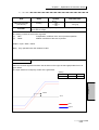
Differential
compensation
Function
Symbol
Execution time
10.2 [µs]
Three times averaging of differentiation values of the input numerical
value is performed and the result is output.
The setting contents of the function argument
(1)
Differential gain:
differential coefficient in the second unit system (when the change in
input is 1.0 per second, 1.0 is output.)
For the sake of safety, averaging is made against a rapid change.
As the operation parameter, mrxxxx can also be used in addition to krxxxx, in which case each
parameter should be set by the user program.
Note) Only operation with real numbers is valid.
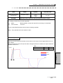
Graph
When the function argument has been set as shown on the right, the trend graph taken from it is
given below.
Differential compensation
Differential gain
kr0000
10.000
In a place where the input value is constant (inclination equaling to 0), the differential value is also
0, and thence the output becomes 0.
The output value changes only in a part where the input value is always changing.
In the trend graph given below, the rapidly changing part is not displayed on the graph.
Chapter 5
Note)
Input
Output
Time
5-39
Chapter 5 Explanations of Instruction Words
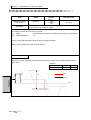
Kind
Name
Data flow language
(Function 2)
Phase compensation
Symbol
Execution time
10.2 [µs]
Phase compensation for the input numerical value is performed and the
result is output.
Function
The setting contents of the function argument
(1)
Reset:
Reset operation of input and output short-circuiting is commanded.
(2)
Phase gain (A):
Depending on whether being greater than 1.0 or not, advanced phase or
lagged phase is set.
(3)
Time gain (T):
Time coefficient in seconds (the time during which the output value
reaches the input value: second)
As the operation parameter, mrxxxx can also be used in addition to krxxxx, in which case each
parameter should be set by the user program.
When the reset is turned ON, short-circuiting between the input and output is performed, whereby
an arbitrary value can be preset.
Note) Only operation with real numbers is valid.
Graph
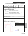
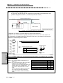
When the function argument has been set as shown on the right, the trend graph taken from it is
given below.
Depending on the time gain, the size of the curve changes that represents the output value that is
coming closer to the input value.
When the gain is small, a small arc is drawn, and when it is large, a large arc is drawn.
Chapter 5
Output 1
Phase compensation
Reset
Phase gain (A1)
Time gain
Phase compensation
Reset
Phase gain (A2)
Time gain
X
Output 1
G00000
kr0000
kr0001
Output 2
kr0002
kr0003
A1
X
X
Time
Output 2
5-40
Input
Output
A2
2.0000
-0.8000
0.6000
1.0000
Chapter 5 Explanations of Instruction Words
Kind
Name
Data flow language
(Function 2)
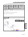
PI compensation
Function
Symbol
Execution time
12.6 [µs]
PI compensation (proportioning, integration) for the input numerical value
is performed and the result is output.
The setting contents of the function argument
(1)
Reset:
Reset operation of input and output short-circuiting is commanded.
(2)
Hold:
Integration hold SW (stopping the integration)
(3)
Proportioning gain:
(4)
Integral gain:
Integral coefficient in the second unit system (the time during which the
output value reaches the input value: second)
(5)
Upper limit value: The upper limit value to be output should be designated.
(6)
Lower limit value: The lower limit value to be output should be designated.
As the operation parameter, mrxxxx can also be used in addition to krxxxx, in which case each
parameter should be set by the user program.
When the reset is turned ON, short-circuiting between the input and output is performed, whereby
an arbitrary value can be preset.
Note) Only operation with real numbers is valid.
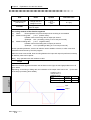
Graph
PI compensation
Reset
Hold
Proportioning gain
Integral gain
Upper limit value
Lower limit value
G00000
G00001
kr0000
kr0001
kr0002
kr0003
0.1000
3.0000
30.000
-30.000
Time
Input
Output
5-41
Chapter 5
When the function argument has been set as shown on the right, the trend graph taken from it is
given below.
Depending on the proportioning gain, the output value at the start changes, and depending on the
integral gain, the inclination of the output value changes.
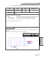
Chapter 5 Explanations of Instruction Words
Kind
Name
Data flow language
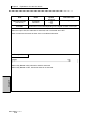
(Function 2)
Limitation on the
change ratio in a
straight line form
Function
Symbol
Execution time
8.4 [µs]
Change ratio limitation on the input numerical value is performed and the
result is output.
The setting contents of the function argument
(1)
Reset:
Reset operation of input and output short-circuiting is commanded.
(2)
Maximum rising ratio:
(> 0.0: positive value):
limitation value of the rising ratio of output per second
(Example: 10.0 = permitting a rising of 10 or less per second)
(3)
Maximum falling ratio:
(< 0.0: negative value):
limitation value of the falling ratio of output per second
(Example: -10.0 = permitting a falling of 10 or less per second)
As the operation parameter, mrxxxx can also be used in addition to krxxxx, in which case each
parameter should be set by the user program.
When the reset is turned ON, short-circuiting between the input and output is performed, whereby
an arbitrary value can be preset.
Note) Only operation with real numbers is valid.
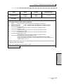
Graph
When the function argument has been set as shown on the right, the trend graph taken from it is
given below.
Depending on the rising or falling ratio, the inclination of the output value can be set. (in the case
of the step input having been added)
Chapter 5
Limitation on the
change ratio in a
straight line form
Reset
Maximum rising rate
Maximum falling rate
G00000
kr0000
kr0001
Input
Output
5-42
0.1000
-0.1000
Chapter 5 Explanations of Instruction Words
Kind
Name
Data flow language
(Function 2)
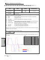
S-form change ratio
limitation
(S-ARC)
Function
Symbol
Execution time
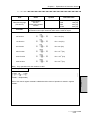
23.4 [µs]
S-form change ratio limitation on the input numerical value is performed
and the result is output.
The setting contents of the function argument
(1)
(2)
(3)
(4)
(5)
(6)
(7)
(8)
Reset:
Reset operation of input and output short-circuiting is commanded.
Maximum rising ratio:
(> 0.0): limitation value of the rising ratio of output per second
Maximum falling ratio:
(< 0.0): limitation value of the falling ratio of output per second
Increasing-rising ratio (> 0.0):
Acceleration increasing value per second when acceleration starts
Decreasing-rising ratio (< 0.0):
Acceleration decreasing value per second when acceleration ceases
Decreasing-decreasing ratio (> 0.0):
Deceleration decreasing value per second when deceleration ceases
Increasing-decreasing ratio (< 0.0):
Deceleration increasing value per second when deceleration starts
S-form acceleration/deceleration ceasing coefficient (>0.0):
Change ratio limitation value when the acceleration/deceleration has ceased
Usually, it should be set at twice the value as obtained by choosing the largest of the
absolute values of (4) - (7).
When the reset is turned ON, short-circuiting between the input and output is performed, whereby
an arbitrary value can be preset.
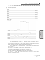
Note) Only operation with real numbers is valid.
Chapter 5
Graph
5-43
Chapter 5 Explanations of Instruction Words
When the function argument has been set as shown on the right, the trend graph taken from it is
given below.
Although the graph is the same as ARC, since the curve right before the straight line (B1 - 4) is
also set, a waveform like an S-form is output.
(Note)
If the input value is changed while accelerating
or decelerating, an overshooting may
S-form limitation on the change ratio
occur.
Reset
Maximum rising rate
Maximum falling rate
Increasing-rising ratio
Decreasing-rising ratio
Decreasing-decreasing ratio
Increasing-decreasing ratio
S-form acceleration/
deceleration ceasing coefficient
Time
Input
Chapter 5
Output
5-44
G00000
kr0000
kr0001
kr0002
kr0003
kr0004
kr0005
10.000
-10.000
0.020
-0.020
0.0020
-0.0020
kr0006
0.0040
Chapter 5 Explanations of Instruction Words
Kind
Name
Data flow language
(Function 3)
Trigonometric
function
Inverse trigonometric
function
Function
Symbol
Execution time
SIN
COS
18.6 [µs]
16.8 [µs]
TAN
30.4 [µs]
ATAN
20.5 [µs]
Trigonometric function (inverse trigonometric function) operation is
performed on the input numerical value and the result is output.
sin function
D2 = sin (D1)
cos function
D2 = cos (D1)
tan function
D2 = tan (D1)
asin function
D2 = sin-1 (D1)
acos function
D2 = cos-1 (D1)
atan function
D2 = tan-1 (D1)
Note) Only operation with real numbers is valid.
Example of use
Sine of the data in register mr0000 is obtained and the result of operation is stored in register
mr0001.
5-45
Chapter 5
mr0001 = SIN(mr0000)
Chapter 5 Explanations of Instruction Words
Kind
Name
Data flow language
(Function 2)
Unconditional
subroutine
Symbol
Execution time
14.0 [µs]
A subroutine is executed unconditionally.
Function
By double clicking on the symbol, a screen for setting an argument appears and the user can set
an argument for the subroutine.
In the subroutine, exchange of data is carried out by means of the stack registers (sr0000, si0000,
SI0000). The setting of stack registers should be made on the screen for setting an argument.
The actual data flow shall be as follows.
Input data
Stack register
Output data
Integer data
→
si0000
→
Integer data
Real number data
→
sr0000
→
Real number data
Relay/coil
→
SI0000
→
Relay/coil
Calling side
Subroutine
Calling side
Chapter 5
Example of use
Subroutine AAAA is executed unconditionally. Registers mi0000, mi0001 are customarily used,
and if you wish to use these data as well, the data in register mi0000 is passed to stack register
si0000 of subroutine AAAA. And when the data that has been calculated in subroutine AAAA is
stored in stack register si0000, the data is stored in register mi0001.
However, if they are not used in subroutine AAAA, the data in mi0000 is stored in mi0001.
5-46
Chapter 5 Explanations of Instruction Words
Kind
Name
Symbol
Execution time
Jump instruction
---
LD language
Label instruction
Jump:
Function
Label:
Jump to the designated circuit or designated label is
performed.
It is used for a label to which a jump is made.
It is regarded as one of the logic circuits.
XXXX stands for the circuit number of label name (4 digits).
Note 1) A jump cannot be performed between subprograms or subroutines.
Note 2) A program that loops at one point can also be created, but it must not be a permanent
loop.
Note 3) On the right side of the label there should be a storing in a register.
When relay B00000 is ON, a jump is made to the line of label ABCD, and the programs between it
and label ABCD are not executed.
When relay B00000 is ON, the data in register kr0000 (10.000) is stored in register mr0000 and 1
is stored in register mi0000.
When relay B00000 is OFF, the data in register kr0000 (10.000) is not stored in register mr0000
and 0 is stored in register mi0000.
5-47
Chapter 5
Example of use
Chapter 5 Explanations of Instruction Words
Kind
Name
Connective
(Store)
Symbol
Execution time
0.10 [µs]
LD language
Connective
(Load)
Function
0.06 [µs]
Storing and loading of the result of logical operation and numerical
operation, to and from the intermediate memory is performed.
It is used when there are 12 or more logical codes or numerical codes arranged in series.
It must be placed between networks without fail.
While 10 sets of symbols can be inserted into 1 circuit, the loading must always be made after the
storing.
Chapter 5
Example of use
5-48
Chapter 5 Explanations of Instruction Words
Kind
Name
LD language
Termination of the
processing of a
subroutine program
Function
Symbol
Execution time
14.0 [µs]
The subroutine program is terminated.
It is used when in a subroutine program you wish to terminate it under a certain condition.
Example of use
Program at the calling side
Subroutine program
Label
Value
si0002
ki0000
5
SI0040
I00000
si0006
Z00009
si0008
mi0000
si000A
mi0001
Chapter 5
When relay I00000 is OFF, the data in register si0002 =
the data in ki0000 (5) is stored in register si0008 and data
(5) is loaded to register mi0000. The data in stack
register si0006 = the data in z0009 is stored in register
si000A and loaded to register mi0001.
Argument
However, when relay I00000 is ON, although the data(5) in stack register si0002 is stored in stack
register si0008 as it is, the data in stack register si0006 at the time of I0000 has been turned ON is
stored in si000A and remains there. (Since z00009 is a 1-mili-counter, if the relay is turned ON
when it is 100, then 100 is stored in si000A. And if I0000 is turned ON, then the data in si0006 is
stored there.)
5-49
Chapter 5 Explanations of Instruction Words
Kind
Name
Data flow language
(Function 2)
(Arithmetic) average
Function
Symbol
Execution time
---
The arithmetic average value of the data corresponding to the input
numerical value that start at the foremost address as has been set by the
argument is obtained and the result is output.
The setting contents of the function argument
(1)
The foremost part of buffer addresses (mrXXXX):
If the input is smaller than 1, then it is regarded as 1, and the value of the first
data is returned.
Chapter 5
Example of use
Argument of arithmetic average
Foremost part of buffer addresses: mr0000
If the setting is made as above, the arithmetic average reads the data in register kr0000 (5.0000)
and the argument, and the result of the operation(12,000):
(mr0000 + mr0001 + mr0002 + mr0003 + mr0004)/5
is stored in register gr0000.
5-50
Chapter 5 Explanations of Instruction Words
Kind
Name
Data flow language
(Function 2)
Filter
Function
Symbol
Execution time
18.8 [µs]
Frequency limitation to the input numerical value is performed and the
result is output.
The setting contents of the function argument
(1)
Reset:
Reset operation of input and output short-circuiting is commanded.
(2)
Lower limit frequency (>0.0 : positive value):
Lower limit frequency of 3 db decrease
(3)
Upper limit frequency (>0.0 : positive value):
Upper limit frequency of 3 db decrease
Note) Only operation with real numbers is valid.
Graph
When the function argument has been set as shown on the right, the trend graph taken from it is
given below.
Filter
G00000
Lower limit frequency
kr0000
0.0001
Upper limit frequency
kr0001
0.0500
Chapter 5
Reset
Time
Input
Output
5-51
Chapter 5 Explanations of Instruction Words
Kind
Name
Data flow language
(Function 2)
PID compensation
Function
Symbol
Execution time
14.8 [µs]
PID compensation for the input numerical value is performed and the
result is output.
The setting contents of the function argument
(1)
Reset:
Reset operation of input and output short-circuiting is commanded.
(2)
Hold:
Integration stop SW
(3)
Zero clear:
A relay is designated that commands the zero reset.
(4)
Proportioning gain:
(5)
Integral gain:
Integral coefficient in the second unit system (the time during which the
output value reaches the input value: second)
(6)
Differential gain: Differential coefficient in the second unit system (when the change in
input is 1.0 per second, 1.0 is output)
(7)
MAX limit:
The upper limit value output is designated.
(8)
MIN limit:
The lower limit value output is designated.
When the reset is turned ON, short-circuiting between the input and output is performed, whereby
an arbitrary value can be preset.
Note) Only operation with real numbers is valid.
Graph
When the function argument has been set as shown on the right, the trend graph taken from it is
given below.
Chapter 5
Filter
Time
Reset
G00000
Hold
G00001
Zero clear
G00002
Proportioning gain
Integral gain
kr0000
kr0001
0.1000
3.0000
Differential gain
kr0002
0.0100
MAX limit
kr0003
30.000
MIN limit
kr0004
-30.000
Input
Output
5-52
Chapter 5 Explanations of Instruction Words
Kind
Name
Data flow language
(Function 2)
Temporary delay
Function
Symbol
Execution time
9.8 [µs]
Temporary delay response to the input numerical value is output.
The setting contents of the function argument
(1)
Reset:
Reset operation of input and output short-circuiting is commanded.
(2)
Time constant:
T second
Turn the reset SW ON without fail at the time of starting operation.
Note) Only operation with real numbers is valid.
Graph
When the function argument has been set as shown on the right, the trend graph taken from it is
given below.
During the period in which the input has been changed by the time constant, the output values are
plotted to draw an arc.
Filter
Output
Reset
G00000
Time constant
kr0000
1.0000
Input
Chapter 5
Output
Time
T
5-53
Chapter 5 Explanations of Instruction Words
Kind
Name
Data flow language
(Function 2)
Delay
(Time delay)
Function
Symbol
Execution time
9.6 [µs]
The delay time that has been set is added to the input numerical value
and the result is output.
The setting contents of the function argument
(1)
Reset:
Reset operation of input and output short-circuiting is commanded.
(2)
Delay time:
T (second)
(3)
Sampling time:
T (second)
The number of samples (T/
T) is valid when it is 1000 or less.
The delay is gone when the reset SW is turned ON.
Note) Only operation with real numbers is valid.
Graph
When the function argument has been set as shown on the right, the trend graph taken from it is
given below.
Depending on the delay time, the input waveform is delayed by T (second) and then output.
Delay
Reset
Chapter 5
Delay time
Sampling time
kr0000
kr0001
Time
T
Input
Output
5-54
5.0000
1.0000
Chapter 5 Explanations of Instruction Words
Kind
Name
Data flow language
(Function 2)
Constant frequency
pulse
Symbol
Execution time
8.0 [µs]
The input numerical value is turned ON/OFF at set intervals and then is
output.
Function
The setting contents of the function argument
(1)
Reset:
Reset operation of input and output short-circuiting is commanded.
(2)
ON time (second):
The time for turning the output ON should be designated.
(3)
OFF time (second):
The time for turning the output OFF should be designated.
Note) Only operation with real numbers is valid.
Graph
When the function argument has been set as shown on the right, the trend graph taken from it is
given below.
Depending on the ON/OFF time, the input waveform is output.
Constant frequency pulse
G00000
ON time
OFF time
kr0000
kr0001
5.0000
3.0000
Chapter 5
Reset
Input
Output
Time
TON
TOFF
5-55
Chapter 5 Explanations of Instruction Words
Kind
Name
Data flow language
(Function 2)
Variable setting
pattern
Function
Symbol
Execution time
12.7 [µs]
Approximation conversion of the input numerical value by line
segmentation with pattern memory is performed and the result is output.
The setting contents of the function argument
(1)
Number of points (> = 2: integer):
Number of input patterns
(2)
Foremost of the pattern buffer (mrXXXX):
the foremost address of the input buffer
While in the pattern, an initial value was set beforehand by means of the pattern data, the real
number value in a circuit can be changed herein.
By accumulating the data that has been obtained in the process control, it can be applied to the
learning control.
Note) Only operation with real numbers is valid.
Graph
Output
P4, Q4
Chapter 5
P3, Q3
P2, Q2
P1, Q1
5-56
Input
P1/Q1
mr0000
mr0001
P2/Q2
mr0002
mr0003
P3/Q3
P4/Q4
mr0004
mr0006
mr0005
mr0007
Chapter 5 Explanations of Instruction Words
Kind
Name
Data flow language
(Function 2)
Upper and lower
limiters
Function
Symbol
Execution time
7.45 [µs]
Upper and lower limiters are added to the input numerical value and it is
then output.
The setting contents of the function argument
(1)
Upper limit:
It designates the upper limit value of the output.
(2)
Lower limit:
It designates the lower limit value of the output.
Note) Only operation with real numbers is valid.
Graph
When the function argument has been set as shown on the right, the trend graph taken from it is
given below.
The input waveform is output by means of the upper and lower limit values.
Upper and lower limiters
kr0000
10.000
Lower limiter value
kr0001
-10.000
Chapter 5
Upper limiter value
Upper limiter value
Time
Lower limiter value
Input
Output
5-57
Chapter 5 Explanations of Instruction Words
Kind
Name
Data flow language
(Function 2)
Hysteresis
Function
Symbol
Execution time
8.4 [µs]
Hysteresis (2-gain amplifier at the time of rising and falling) is added to
the input numerical value and it is then output.
The setting contents of the function argument
(1)
Reset: It makes:
Output value = Input value × G1
(2)
Gain at the low side:
G1 (0.0 < G1 < G2)
(3)
Gain at the high side:
G2 (0.0 < G1 < G2)
When the input data is rising, G1 is valid, and when falling G2 is valid.
The output remains at a certain value at the time of switching from rising to falling, or from falling to
rising.
Turn the reset SW ON without fail at the time of starting operation.
Note) Only operation with real numbers is valid.
Graph
According to the history of changes in the input data, the output data is plotted as the curve given
in the figure below.
Output
)2
Chapter 5
)1
Input
0
)1
)2
5-58
Chapter 5 Explanations of Instruction Words
Kind
Name
Data flow language
(Function 3)
Scaling
Function
Symbol
Execution time
7.27 [µs]
Scaling (sum of product operation) is added to the input numerical value
and it is then output.
The setting contents of the function argument
(1)
Gain:
multiplication coefficient of the sum of product operation
(2)
Offset:
addition coefficient of the sum of product
Output = Input * Gain + Offset
Note) Only operation with real numbers is valid.
Graph
When the function argument has been set as shown on the right, the trend graph taken from it is
given below.
The input waveform is output by means of the gain/offset.
Scaling
kr0000
1.0000
Offset
kr0001
5.0000
Chapter 5
Gain
Offset
Time
Input
Output
5-59
Chapter 5 Explanations of Instruction Words
Kind
Name
Data flow language
(Function 3)
Backlash
Function
Symbol
Execution time
8.8 [µs]
Backlash (a kind of integral compensation) is added to the input
numerical value and it is then output.
The setting contents of the function argument
(1)
Reset:
Reset operation of input and output short-circuiting is commanded.
(2)
Width of backlash:
W
Turn the reset SW ON without fail at the time of starting operation.
Note) Only operation with real numbers is valid.
Graph
When the function argument has been set as shown on the right, the trend graph taken from it is
given below.
Backlash
W
G00001
Width of backlash
kr0000
20.000
Input
Output
W
Chapter 5
Reset
2
Time
5-60
Chapter 5 Explanations of Instruction Words
Kind
Name
Symbol
Data flow language
(Function 3)
Backlash
compensation
Execution time
8.2 [µs]
Backlash compensation (a kind of differential compensation) is
performed to the input numerical value and it is then output.
Function
The setting contents of the function argument
(1)
Reset:
Reset operation of input and output short-circuiting is commanded.
(2)
Width of backlash:
W
Turn the reset SW ON without fail at the time of starting operation.
Note) Only operation with real numbers is valid.
Graph
When the function argument has been set as shown on the right, the trend graph taken from it is
given below.
Backlash compensation
Reset
G00001
Width of backlash
kr0000
20.000
W
2
W
W
W
2
2
Chapter 5
2
Time
W
2
W
2
Input
Output
5-61
Chapter 5 Explanations of Instruction Words
Kind
Name
Data flow language
(Function 2)
Conditional
subroutine
Function
Symbol
Execution time
A subroutine is executed depending on the logical condition of the input.
When the input is ON, the subroutine is executed, and not executed when OFF.
Other contents are the same as those of the unconditional subroutine.
Example of use
Chapter 5
When relay B00000 is ON, subroutine AAAA is executed.
When relay B00000 is OFF, subroutine AAAA is not executed.
5-62
--
Chapter 5 Explanations of Instruction Words
Kind
Name
Data flow language
(Function 3)
Binary Gray code
Symbol
Execution time
--
The input numerical is read as an integer data, converted to a Gray code,
and it is then output.
Function
Note) It performs the reverse operation of the Gray code conversion
. Pay attention not to
mix them up.
Example of use
The data in register mi0000 is read as a 16-bit integer, converted to a Gray code, and it is then
output.
If the data in register mi0000 is (10), then (15) is stored in mi0001.
D2
Gray
0000
0001
0011
0010
D1
Integer
0100
0101
0110
0111
D2
Gray
0110
0111
0101
0100
D1
Integer
1000
1001
1010
1011
D2
Gray
1100
1101
1111
1110
D1
Integer
1100
1101
1110
1111
10
1010
1111
15
Input
Integer
Gray code
Output
D2
Gray
1010
1011
1001
1000
Chapter 5
D1
Integer
0000
0001
0010
0011
5-63
Chapter 5 Explanations of Instruction Words
Kind
Name
Data flow language
(Function 3)
Divisor and remainder
Function
Symbol
Execution time
--
The divisor for the input numerical value and the remainder are output.
The setting contents of the function argument
(1)
(2)
Divisor (integer):
Remainder (integer):
Number to divide the input numerical value
Register to store the remainder
Example of use
If the argument of DIVMOD is set as shown on the
right, the remainder when the data in register
mi0000 is divided by the divisor ki0000 (7) is stored
in register mi0002. Also, the quotient is stored in
register mi0001.
DIVMOD
Argument
Label
Value
Divisor (integer)
ki0000
7
Remainder (integer)
mi0002
Chapter 5
If the data in register mi0000 is (10), then (1) is stored in register mi0001 as the quotient, and (3) is
stored in register mi0002 as the remainder.
5-64
Chapter 5 Explanations of Instruction Words
Kind
Name
Symbol
Execution time
ON timer (TSTD)
Data flow language
(Function 3)
-OFF timer (TRTC)
Function
It has gathered the ON timer relay (TS, TD) and the OFF timer relay (TR,
TC) in one line, and the operation is the same.
TSTD: If the input bit is turned ON, the coil is turned ON after the time set by the argument has
lapsed.
↓ With this, what was written in 2 lines can be written in 1 line.
The setting contents of the function argument
[1]
Timer value (real number): It sets the time for turning the coil ON after the designated time
has lapsed.
Chapter 5
TRTC: If the input bit is turned OFF, the coil is turned OFF after the time set by the argument has
lapsed.
↓ With this, what was written in 2 lines can be written in 1 line.
The setting contents of the function argument
[1]
Timer value (real number): It sets the time for turning the coil OFF after the designated time
has lapsed.
5-65
Chapter 5 Explanations of Instruction Words
Example of use
After relay B00000 is turned ON, upon lapse of the time set by TSTD, relay B00001 is turned ON.
•
B000
•
B000
Set time
Within 1 scan
After relay B00010 is turned OFF, upon lapse of the time set by TRTC, relay B00011 is turned
OFF.
B00010
Chapter 5
B00011
Set time
Within 1 scan
5-66
Chapter 5 Explanations of Instruction Words
Kind
Name
Data flow language
(Function 3)
Function
Symbol
Execution time
ON differential
(USUC)
-OFF differential
(DSDC)
It has gathered the ON differential relay (US, UC) and the OFF
differential relay (DS, DC) in one line, and the operation is the same
except that it is without the 1 scan delay.
USUC: If the input bit is turned ON, 1 scan is turned ON without the 1 scan delay.
↓ With this, what was written in 2 lines can be written in 1 line.
DSDC: If the input bit is turned OFF, 1 scan is turned ON without the 1 scan delay.
Chapter 5
↓ With this, what was written in 2 lines can be written in 1 line.
5-67
Chapter 5 Explanations of Instruction Words
Example of use
When B00000 is turned ON, after a delay for 1 scan, B00001 is turned ON for 1 scan, but B00002
is turned ON for 1 scan immediately after B00000 has been turned ON without the 1 scan delay.
B00000
US0000
UC0000
B00001
B00002
Chapter 5
When B00010 is turned ON, after a delay for 1 scan, B00011 is turned ON for 1 scan, but B00012
is turned ON for 1 scan immediately after B00010 has been turned ON without the 1 scan delay.
B00010
DS0000
DC0000
B00011
B00012
5-68
Chapter 5 Explanations of Instruction Words
Kind
Name
Data flow language
(Function 4)
SET
RESET
SET:
Function
RESET:
Symbol
Execution time
-
When the input bit is turned ON, the designated output bit is
kept to ON.
When the input bit is turned OFF, the designated output bit
is kept to OFF.
SET: Note) While SET is ON, the contact set by the argument is turned OFF, when RESET is
turned ON.
The setting contents of the function argument
[1]
SET coil: It designates the relay to be kept to ON.
RESET: Note) While RESET is ON, the contact set by the argument is not turned ON, even
when SET is turned ON.
The setting contents of the function argument
[1]
RESET coil: It designates the relay to be kept to OFF.
Chapter 5
Example of use
If B00000=ON, then B00010=ON, and the value in mi0001 is stored in mi0002.
If B00001=ON, then B00010=OFF, and the value in mi0000 is stored in mi0002.
B00000 (SET coil)
B00001 (RESET coil)
B00010 (Output)
If B00000=ON, then B00010=ON. (even when B00000=OFF, not that B00010=OFF)
If B00001=ON, then B00010=OFF. (even when B00000=ON, not that B00010=ON)
If B00001=OFF, now that B00000=ON, and so B00010=ON.
5-69
Chapter 5 Explanations of Instruction Words
Kind
Name
Data flow language
(Function 4)
Counter
(UPDOWN)
Symbol
Execution time
--
This has gathered the counters (NR, NP, NU, ND, NZ and n0) in 1 line,
and the operation is the same.
Function
The setting contents of the function argument
[1]
Reset coil:
It sets the relay that makes the present value of count 0.
[2]
Preset coil:
It sets the relay that makes the present value of count become
the value set by the count preset value.
[3]
Upcoil:
It sets the present value of count to be incremental.
[4]
Downcoil:
It sets the present value of count to be decremental.
[5]
Zero detection contact:
It sets the relay that notifies that the present value of count has
become zero.
[6]
Present value of count:
It sets the register to store the present value.
[7]
Count preset value:
It sets the value to be set to the present value of count when
the preset coil has been turned ON.
Chapter 5
Example of use
↓ With this, what was written in 5 lines can be written in 1 line.
5-70
Chapter 5 Explanations of Instruction Words
Kind
Name
Data flow language
(Function 4)
Data transfer
(MOVW/MOVWD)
Symbol
Execution time
--
It transfers the designated data to the designated label in units of words.
Function
The setting contents of the function argument
[1]
Label of transferrer:
It designates the foremost address from which the data is
transmitted.
[2]
Label of transferee:
It designates the foremost address where the data is received.
[3]
Offset of transferrer:
It designates the number of interval between the label of
transferrer and the address from which the data is transmitted.
(for MOVW only)
[4]
Offset of transferee:
It designates the number of interval between the label of
transferee and the address where the data is received. (for
MOVW only)
[5]
Number to be transferred: It designates the number of data to be transferred.
Example of use
When the setting is made as shown on the right, the data of 5 words is transferred from mi000A to
b00004.
Label
Label of transferrer
mi0000
Value
mi000A
b00004
mi000B
b00005
Label of transferee
b00000
mi000C
b00006
Offset of transferrer
ki0000
mi000D
b00007
Offset of transferee
ki0001
4
mi000E
b00008
Number to be
transferred
ki0002
5
10
Chapter 5
MOVW
Argument
5-71
Chapter 5 Explanations of Instruction Words
Kind
Name
Symbol
Execution time
Integer conversion
Data flow language
(Function 3)
Function
-Real number
conversion
The designated data is converted to the designated type and the result is
output.
TODINT (the real number input is converted to a 32-bit integer)
The setting contents of the function argument
[1]
Transferrer (2 points used: even address) It designates the address where the input real
number data is converted to a 32-bit integer and output.
[2]
Transferee (2 points used: even address + 1) It designates the address where the sign is
output when the input real number data is converted to a 32-bit integer.
TOREAL (the 32-bit integer input is converted to a real number)
The setting contents of the function argument
[1]
Transferrer (2 points used:even address) It designates the address where the input 32-bit
integer data is converted to a real number and output.
[2]
Transferee (2 points used:even address + 1) It designates the address where the sign is
output when the input 32-bit integer data is converted to a real number.
Chapter 5
Example of use
In the case of TODINT, if the setting is made as
shown on the right and the data in the input real
number register mr0000 is (-12.5600), then:
mi0010 = -13, mi0011 = -1
In the case of TOREAL, if the setting is made as
shown on the right, then:
mr0011 = 131082
mr0011 = ki0000 + ki0001 * 65536
= 10 + 2 * 65536
= 10 + 131072
= 131082
5-72
TODINT
Argument
Label
Transferrer
(even address)
Transferee
(even address + 1)
mi0010
Value
mi0011
TOREAL
Argument
Label
Transferrer
(even address)
Transferee
(even address + 1)
ki0000
Value
10
ki0001
2
Chapter 5 Explanations of Instruction Words
Kind
Name
Data flow language
(Function 4)
Bank switching
(F_BANK)
Function
Symbol
Execution time
--
It is used to synchronize the data in the broadcast communications area
to be used in the FL-net module.
The setting contents of the function argument
[1]
Post number of the SX bus to be switched (integer):
Post number of the SX bus of the module (FL-net) for which bank
switching is to be made
[2]
Status (integer): If the operation is normal, 0 is input, and if not, the following error code is
input.
64: A post number of the SX bus has been designated that is not the
destination module.
65: Multiple bank switching requests of 1 CPU have been made.
66: While processing bank switching, access errors have occurred in
the processor bus.
[3]
In process flag (bit):
It is turned ON while the bank switching is in process.
[4]
Error flag (bit):
It is turned ON for 1 scan when an error occurs.
Note) When using the bank switching, the correct setting of parameters of the FL-net module
should be made in the system configuration definition. Without the correct setting, normal
operation cannot be guaranteed.
At the 1st scan, the in process flag is turned ON.
At the 2nd scan, the completion flag is turned ON, and immediately thereafter the in process flag is
turned OFF.
Transmittal and receiving of data should be done while the completion flag is ON.
At the 3rd scan, the completion flag is turned OFF.
At the 4th scan, the in process flag is turned ON.
The rest is the repetition of the above.
In the transmittal and receiving of continuous data, the data that is actually passed over is the data
when the completion flag has been turned ON, which occurs once every 3 scans.
Completion flag
In process flag
Within 1 scan
1 scan
5-73
Chapter 5
Internal operation of the F_BANK function
Chapter 5 Explanations of Instruction Words
Example of use
Parameters of each function should be set as
shown on the right.
F_BANK
Since B00020 is a B-contact, at first the F_BANK
function is executed and the in process flag is
turned ON.
At the next scan the completion flag (B00020) is
turned ON, and the transfer of data (MOVWD)
should be made at this timing.
When B00020 is turned ON, since the first one is a
B-contact, B00020 is turned OFF, returning to the
initial state.
Chapter 5
By repeating the above, the data transfer
(MOVWD) is carried out.
5-74
Argument
Label
Value
Post number of the
SX bus to be
switched
Status
ki0000
7
mi0000
In process flag
B00001
Error flag
B00002
MOVWD
Label of transferrer
g00000
Label of transferee
fi0000
Number to be
transferred
ki0001
MOVWD
Label of transferrer
10
fi0100
Label of transferee
g00100
Number to be
transferred
ki0002
10
Chapter 5 Explanations of Instruction Words
Kind
Name
Data flow language
(Function 4)
Remote data read
Function
Symbol
Execution time
--
The data of the equipment that is connected to the network is read out by
designating the address directly, via a communications module.
The setting contents of the function argument
[1]
Post number of the SX bus:
Post number of the SX bus of the communications module by way of
which the reading is made
[2]
Channel number: Channel number of the communications module
[3]
Node number:
Node number of the destination of communications
[4]
Variable designation method:
It should be designated for each object of access of the destination of
communications (see < About the variable designation method >)
[5]
Foremost address of variable designation:
It designates the foremost address by which the type of data to be read
is designated.
(see < Support message list>)
[6]
Read data size:
It designates the word size of the read data.
[7]
Foremost address of the read data:
It designates the foremost address of the read data.
[8]
Error flag:
When the reading has not been done normally, it is turned ON for 1
scan.
[9]
Status:
It displays the contents of the error flag. They are given below.
More detailed contents will be explained in the examples of use.
The following are the values that are input into the status when an error flag has been turned ON.
68
Name
Abnormal memory address
designation
69
Memory size exceeded
160
Abnormal designation of the
destination of communications
171
Internal resources used up
193
Abnormal channel open
195
Abnormal message
transmission
201
No vacant port
206
Transfer size exceeded
Cause
When there is an error in the address designated by [5].
When the address designated by [5] + [6] exceed the effective
range of the address. In this case the value of the read data is not
guaranteed.
When [4] =0 and there is no CPU number of the destination of
communications
When the internal resources to execute R_READ, R_WRIT have
been used up. Or when multiple numbers are started
simultaneously, the internal resources may be used up. In this
case, restart the controller after a while.
When an abnormal value is set in [2].
When an abnormal value is set in [2].
When an abnormal value is set in [3].
When a value other than the type codes is set as the memory type.
When trying to open more ports than the specified number in 1
communications module.
When a value other than “0” has been set as the variable
designation method, and the limitation value of the message data
size of the communications module by way of which the reading is
made has been exceeded.
5-75
Chapter 5
Code
Chapter 5 Explanations of Instruction Words
< About the variable designation method >
The contents to be set at the variable designation method of R_READ and R_WRIT are indicated
herein. The variable designation method is specified for each object of access of the destination
of communications.
[1]
When the variable designation method = 0
It is designated when the memory on CPU of the ǴGPCsx system is used via a network
(not dependent on its type).
F
Name
Memory type code
CPU number
0
Standard memory
1
Memory type
Lower address
Retain memory
User FB memory
3
5
Higher address
System FB memory
9
System memory
10
Note) Do not designate other values than 1, 3, 5, 9
and 10 as the memory type code.
[2]
When the variable designation method = 2
It is designated when using the equipment that is connected to a network of OPEN
specifications such as JPCN1.
F
0
Effective size
-
Address 1
-
.
.
-
Address n
Chapter 5
Note) In this case, effective data should be input in the lower 8 bits of an
array of which width is 16 bits.
This is because 8-bit data cannot be handled in the µGPCsx system.
5-76
Chapter 5 Explanations of Instruction Words
< Support message list >
A support message list for the message transmission to be set in the variable designation address
is indicated below. The value that is actually used in a function is the request part of the
processing code. The number of parameters is set at the foremost address, lower 8 bits of the
request command are set at the second, and higher 8 bits are set at the third.
No.
Type of message
[1]
Byte block readout
[2]
Note 2)
Processing code
(TCD code Note 1)
Request
Response
65003 (FDEB)
65203 (FEB3)
Byte block write Note 2)
65004 (FDEC)
65204 (FEB4)
[3]
Word block readout
65005 (FDED)
65205 (FEB5)
[4]
Word block write
65006 (FDEE)
65206 (FEB6)
[5]
Network parameter readout
65007 (FDEF)
65207 (FEB7)
[6]
Network parameter write
65008 (FDF0)
65208 (FEB8)
Stop
65009 (FDF1)
65209 (FEB9)
Start
65010 (FDF2)
65210 (FEBA)
[8]
Profile readout
65011 (FDF3)
65211 (FEBB)
[9]
Communications log readout
65013 (FDF5)
65213 (FEBD)
[10]
Communications log clear
65014 (FDF6)
65214 (FEBE)
[11]
For use for message return test
65015 (FDF7)
65215 (FEBF)
[7]
[12]
Permeable type message
Address readout
SX
reserved
00000 - 59999
(0000 - EA5F)
100 (64)
150 (96)
Address write
101 (65)
151 (97)
Loader command
200 (C8)
250 (FA)
Message function used
R_READ
(variable designation method = 2)
R_WRIT
(variable designation method = 2)
R_READ
(variable designation method = 2)
R_WRIT
(variable designation method = 2)
R_READ
(variable designation method = 2)
R_WRIT
(variable designation method = 2)
R_WRIT
(variable designation method = 2)
R_WRIT
(variable designation method = 2)
R_READ
(variable designation method = 2)
R_READ
(variable designation method = 2)
R_WRIT
(variable designation method = 2)
R_WRIT
(variable designation method = 2)
M_SEND/M_RECEIVE
R_READ
(variable designation method = 0)
R_WRIT
(variable designation method = 0)
-
Message
data size
Number of
parameters
(Note 5)
476 bytes
6
476 bytes
6
476 bytes
6
476 bytes
6
56 bytes
2
20 bytes
2
-
2
-
2
480 bytes
2
480 bytes
4
-
2
1024 bytes
2
1026 bytes
(Note 3)
-
- (Note 4)
-
- (Note 4)
-
492 bytes
-
(
Note 2)
Since the ǴGPCsx does not support the data type of byte, it cannot accept the “byte block readout”, or “byte
block write” request given by the destination node.
) is a hexadecimal representation.
Note 3)
It is a value containing TCD codes.
Note 4)
The maximum size is the maximum value of the memory area designated by each CPU module.
Note 5)
The number of parameters is the number of parameters set by the variable designation.
Example)
Chapter 5
Note 1)
For instance, when the network parameter read is used, at the foremost address of
the variable designation, the number of parameters (2 in this case) is set at the first,
lower 8 bits (EF) of the value of the request part (FDEF) of the processing code are
set at the second, and higher 8 bits (FD) are set at the third.
5-77
Chapter 5 Explanations of Instruction Words
< Virtual address space >
Memory of the µGPCsx
Virtual address space
Input and output memory
00 h -
Standard memory
02 h -
Retain memory
04 h -
System memory
08 h -
In the case of the memory map (default value) of the high-performance CPU module NP1PS-32,
access to each memory is carried out as in the figure below.
Memory map
15
0
Input and output memory
512 words
(fixed)
00000000 h
.
000001FF h
Standard memory
02000000 h
.
020007FF h
(high-speed 2 k words)
(8 k words)
Retain memory
4 k words
02000800 h
.
02001FFF h
Note 2) The size of each memory varies depending on
the model of CPU used.
04000000 h
.
04000FFF h
Note 3) If the data is written into the system memory
by mistake, it may cause malfunctioning or
stop due to a serious failure. (The system
operation cannot be guaranteed.)
Chapter 5
Instance memory
for user FB
4 k words
Instance memory
for system FB
4 k words
System memory
512 words
(fixed)
5-78
Note 1) The virtual address of input and output varies
depending on the system configuration, and is
complicated. It is recommended that for the
sake of simplification, you should transfer the
desired access area first to the internal
memory such as the standard memory, and
gain access to such internal memory.
10000000 h
.
100001FF h
Chapter 5 Explanations of Instruction Words
< Details of the support message >
[1]
Byte block readout
It is a function to read out data in units of bytes (in units of 8 bits for 1 address) via the
FL-net from the virtual address space (32-bit address space) of the destination node. For
the address map of the virtual address space, refer to the specifications of each node.
(Variable designation method=2, readout request code=FDEB)
Request message FDEB (h)
FL-net
Virtual address space
8 bits
Response
message FDB3 (h)
Destination node
0
1
Node number 2
Post number of the SX bus:
(CPU number: 8)
2
.
.
.
246
FFFFFFFF
Fig.1 Image of byte block readout
< Example of a byte block readout program >
This is an example of reading out data of 12 words from the virtual address: 00000000(h) of CPU
connected to the FL-net unit of node number “2”. The value of variable designation format as
given below is set one by one starting at the foremost address of variable designation: mi0000.
Foremost address of variable designation
Processing code
Fig. 2 Relation between the byte block
readout circuit diagram and the variable
designation format
Note 1)
Note 2)
The channel number of the NP1L-FL1 is
fixed at “0”.
The size of the readout data should satisfy
the following:
FD
EB
FD
00
00
00
00
EB
Virtual address
00000000 (h)
Argument
Post number of the SX bus
Channel number
Node number
Variable designation method
Foremost address of variable
designation
Readout data size
Foremost address of readout data size
Chapter 5
Variable designation format
Effective size = 6 (h)
TCD (L)
TCD (H)
Virtual address (LL)
Virtual address (LH)
Virtual address (HL)
Virtual address (HH)
Label Value
ki0000
246
ki0001
0
ki0002
2
ki0003
2
mi0000
ki0004
b00001
12
(Amount of the readout data (number of words)) ≤
(Size of the received data)
5-79
Chapter 5 Explanations of Instruction Words
[2]
Word block readout
It is a message function to read out data in units of words (in units of 16 bits for 1 address)
via a network from the virtual address space (32-bit address space) of the destination node.
For the address map of the virtual address space, refer to the specifications of each node.
(Variable designation method = 2, readout request code=FDED)
Request message FDED (h)
FL-net
Virtual address space
Response
message FEB5 (h)
16 bits
Destination node
0
1
Node number 2
Post number of the SX bus:
(CPU number: 8)
2
.
.
.
246
Fig.3 Image of word block readout
< Example of a word block readout program >
This is an example of reading out data of 10 words from the virtual address: 00000000(h) of CPU
connected to the FL-net unit of node number “2”. The value of variable designation format as
given below is set one by one starting at the foremost address of variable designation: mi0000.
Foremost address of variable designation
Chapter 5
Processing code
Variable designation format
Effective size = 6 (h)
TCD (L)
TCD (H)
Virtual address (LL)
Virtual address (LH)
Virtual address (HL)
Virtual address (HH)
Fig. 4 Relation between the word block
readout circuit diagram and the variable
designation format
Note 1)
Note 2)
The channel number of the NP1L-FL1 is
fixed at “0”.
The size of the readout data should satisfy
the following:
(Amount of the readout data (number of words)) ≤
(Size of the received data)
5-80
FD
ED
FD
00
00
00
00
ED
Virtual address
00000000 (h)
Argument
Post number of the SX bus
Channel number
Node number
Variable designation method
Foremost address of variable
designation
Readout data size
Foremost address of readout data size
Label Value
ki0000
246
ki0001
0
ki0002
2
ki0003
2
mi0000
ki0004
b00001
10
Chapter 5 Explanations of Instruction Words
[3]
Network parameter readout
It is a message function to read out network parameters of the destination node from
Network.
(Variable designation method=2, readout request code=FDEF)
In the network parameter readout, the following information is read out.
FL-net
Request message FDEF (h)
Response
message FEB7 (h)
0 Node name
Destination
node
Node number 2
Fig. 5 Image of the network parameter data
+4
+5 Not used
+9
+10 Manufacturer’s model
+14
+15
+16
+17
+18
+19
+20
+21
+22
+23
+24
+25
+26
+27
Foremost address of common memory area 1
Size of common memory area 1
Foremost address of common memory area 2
Size of common memory area 2
Time for the timeout of token monitoring
Not used
Not used
Not used
Not used
Minimum allowable frame interval
State of the FA link
Protocol version
State of the upper layer
Setting value of the refresh cycle allowable time: RCT
Measured value of the refresh cycle (present value)
Measured value of the refresh cycle (maximum value)
Measured value of the refresh cycle (minimum value)
< Example of a network parameter readout program >
The network parameters of the FL-net unit of node number “2” are read out.
The parameters of variable designation format are input one by one starting at the foremost
address of variable designation: mi0000.
Foremost address of variable designation
Processing code
Fig. 6 Relation between the network
parameter readout circuit diagram and the
variable designation format
Note 1) The channel number of the NP1L-FL1 is
fixed at “0”.
Note 2) Since there are 28 words in the network
parameters, the readout data size should be
set at 28 or more
FD
EF
EF
FD
Argument
Post number of the SX bus
Channel number
Node number
Variable designation method
Foremost address of variable
designation
Readout data size
Foremost address of readout data size
Chapter 5
Variable designation format
Effective size = 2
TCD (L)
TCD (H)
Label Value
ki0000
246
ki0001
0
ki0002
2
ki0003
2
mi0000
ki0004
b00001
28
5-81
Chapter 5 Explanations of Instruction Words
Fig. 6 Relation between the network
parameter readout circuit diagram and the
variable designation format
Chapter 5
Note 1) The channel number of the NP1L-FL1 is
fixed at “0”.
Note 2) Since there are 28 words in the network
parameters, the readout data size should be
set at 28 or more.
Note 3) Note that the address is different from the
common memory that is referred to by the
FLRAS function.
5-82
Argument
Post number of the SX bus
Channel number
Node number
Variable designation method
Foremost address of variable
designation
Readout data size
Foremost address of readout data size
Label Value
ki0000
246
ki0001
0
ki0002
2
ki0003
2
mi0000
ki0004
b00001
28
Chapter 5 Explanations of Instruction Words
[4]
Profile readout
It reads out from the network the system parameters (inherent information) of the
destination node.
There are 2 parameters as the system parameter.
· Common parameter (indispensable) → Only common parameters are available for the
NP1L-FL1.
· Parameter inherent to the device (arbitrary)
(Variable designation method = 2, readout request code = FDF3)
Request message FDF3 (h)
FL-net
Response
message FEBB (h)
Destination node
Node number 2
Common parameter
Parameter inherent to the device
Fig. 7 Image of the Profile readout
< Example of a network parameter readout program >
The network parameters of the FL-net unit of node number “2” are read out.
The parameters of variable designation format are input one by one starting at the foremost
address of variable designation: mi0000.
Foremost address of variable designation
Processing code
FD
EF
EF
FD
Fig. 8 Relation between the profile readout circuit diagram and the variable designation format
Note 1) The channel number of the NP1L-FL1 is
fixed at “0”.
Note 2) The size of readout data should satisfy the
following.
(Amount of the data to be read out (number
of words)) ≤ (Size of the received data)
Note 3) For the readout data size, refer to the profile
use of the destination node.
In the case of the NP1L-FL1, the size of
profile is 113 bytes.
Therefore, the word size to be read out
should be designated as 57 words.
Argument
Post number of the SX bus
Channel number
Node number
Variable designation method
Foremost address of variable
designation
Readout data size
Foremost address of readout data size
Label Value
ki0000
246
ki0001
0
ki0002
2
ki0003
2
mi0000
ki0004
b00001
28
5-83
Chapter 5
Variable designation format
Effective size = 2
TCD (L)
TCD (H)
Chapter 5 Explanations of Instruction Words
[5]
Communications log data readout
It is a function to read out from the network the log information of the destination node.
(Variable designation method = 2, readout request code = FDF5)
Request message FDF5 (h)
FL-net
Response
message FEBD (h)
Destination node
Node number 2
Communications log data
Fig. 9 Image of the communications log data readout
< Example of a setting of communications log data readout argument >
It reads out the communications log data (512 bytes) of the FL-net unit of node number “2”.
The parameters of variable designation format are input one by one starting at the foremost
address of variable designation: mi0000.
Foremost address of variable designation
Processing code
Chapter 5
Variable designation format
Effective size = 4 (h)
TCD (L)
TCD (H)
Readout address(L)
Readout address(H)
FD
F5
F5
FD
00 fixed
Fig. 10 Relation between the communications log data readout circuit diagram and the variable
designation format
Note 1) The channel number of the NP1L-FL1 is
fixed at “0”.
Note 2) The communications log data is 512 bytes
(fixed) for every node of the FL-net.
However, there are indispensable items and
arbitrary items in the supplied items. For
details, check the specifications of each
node.
Also, the amount of data that can be read
out at 1 time is 239 words (480 bytes).
Hence, the read out needs to be made 2
times.
5-84
Argument
Post number of the SX bus
Channel number
Node number
Variable designation method
Foremost address of variable
designation
Readout data size
Foremost address of readout data size
Label Value
ki0000
246
ki0001
0
ki0002
2
ki0003
2
mi0000
ki0004
b00001
17
Chapter 5 Explanations of Instruction Words
Example of use
The figure blow is an example of the readout of network parameters.
In this configuration, 1 unit each of CPU and FL-net module are mounted on 1 base, and
communications are carried out between 2 bases by means of the FL-net.
Argument
Post number of the SX bus
Channel number
Node number
Variable designation method
Foremost address of variable
designation
Readout data size
Foremost address of readout data
size
Error Flag
Status
Label
ki0000
ki0001
ki0002
ki0003
mi0000
Value
246
0
2
2
ki0004
b00001
17
G00000
mi0010
For the variable designation method, since the FL-net module is used in this case, it is “2”.
For the foremost address of variable designation, the foremost label should be designated from
which the parameters to be set will be read. (In this case, it is mi0000.) Next, the number of
parameters should be set to the designated label, and in this case since it is 2, mi0000=2, and
then referring to the support message list, lower 8 bits: 239 (EF) of the applicable request
command 65007 (FDEF) should be set to mi0001, and upper 8 bits: 253 (FD) should be set to
mi0002.
As for the readout data size, since there are 28 words in the case of the network parameters, a
value not smaller than this figure should be set.
As for the foremost address of the readout data, the foremost address of the label from which the
readout data should be read.
Error flag should be turned ON for 1 scan when there has been a readout failure.
Status should indicate the contents of error when the error flag has been turned ON.
With the foregoing setting, information on the module that is mounted on other base board can be
obtained.
Note 1) Note that the value of the network parameter is similar to that of the FLRAS function, but the address
is different.
Note 2) Note that the contents of data at the time of reading are different from those at the time of writing.
5-85
Chapter 5
For the post number of the SX bus, the post
number of the SX bus of the destination of
communications should be set. (In this case,
since the equipment is the FL-net module,
ki0000 = 246.)
Channel number is fixed at “0” in the case of the
FL-net module.
Node number is the 2nd FL-net module, and
hence it is “2”.
Chapter 5 Explanations of Instruction Words
Kind
Name
Data flow language
(Function 4)
Remote data write
(RWRITE)
Symbol
Execution time
--
It writes data onto the equipment that is connected to the network by
designating the address directly, via a communications module.
The setting contents of the function argument
[1]
Post number of the SX bus:
Post number of the SX bus of the module by way of which the
communications are made
[2]
Channel number: Channel number of the communications module
[3]
Node number:
Node number of the destination of communications
[4]
Variable designation method:
It should be designated for each object of access of the destination of
communications (see the next page)
[5]
Foremost address of variable designation:
It designates the foremost address by which the type of data to be
written is designated.
[6]
Written data size: It designates the word size of the written data.
[7]
Foremost address of the written data:
It designates the foremost address of the written data.
[8]
Error flag:
When the writing has not been done normally, it is turned ON for 1 scan.
[9]
Status:
It displays the contents of the error flag. They are given below.
Function
More detailed contents will be explained in the examples of use.
Chapter 5
Code
Name
35
Abnormal transmission
interlock
68
Abnormal memory address
designation
69
Memory size exceeded
160
Abnormal designation of the
destination of communications
171
Internal resources used up
177
Abnormal parameters
193
Abnormal channel open
201
No vacant port
5-86
Cause
When the module with which communications are made is
interlocked. The transmission interlock is performed when an
instance screen is opened and there is operations such as
downloading, etc. Retry if this error has occurred.
When there is an error in the address designated by [5].
When the address designated by [5] + [6] exceed the effective
range of the address. In this case the value of the read data is not
guaranteed.
When [4] =0 and there is no CPU number of the destination of
communications
When the internal resources to execute R_READ, R_WRIT have
been used up. Or when multiple numbers are started
simultaneously, the internal resources may be used up. In this
case, restart the controller after a while.
When 0 is input in [6].
When a value other than those designated in the variable
designation method has been input.
When a value has been input that exceeds the range of values that
can be used as the post number of the SX bus.
When an abnormal value is set in [2].
When trying to open more ports than the specified number in 1
communications module.
Chapter 5 Explanations of Instruction Words
Transfer size exceeded
When a value other than “0” has been set as the variable
designation method, and the limitation value of the message data
size of the communications module by way of which the reading is
made has been exceeded.
Chapter 5
206
5-87
Chapter 5 Explanations of Instruction Words
[1]
Byte block write
It is a function to write data in units of bytes (in units of 8 bits for 1 address) via the FL-net
onto the virtual address space (32-bit address space) of the destination node. For the
address map of the virtual address space, refer to the specifications of each node.
(Variable designation method = 2, write request code = FDEC)
Request message FDEC (h)
FL-net
Virtual address space
Response
message FEB4 (h)
8 bits
Destination node
0
1
2
Post number of the SX bus:
(CPU number: 8)
.
.
.
246
FFFFFFFF
Fig. 1 Image of the byte block write
< Example of a byte block write program >
This is an example of writing data of 5 words onto the virtual address: 64(h) and thereafter of CPU
connected to the FL-net unit of node number “2”. The parameters of variable designation format
are input one by one starting at the foremost address of variable designation: mi0000.
Foremost address of variable designation
Chapter 5
Processing code
Variable designation format
Effective size = 6 (h)
TCD (L)
TCD (H)
Virtual address (LL)
Virtual address (LH)
Virtual address (HL)
Virtual address (HH)
FD
EC
FD
64
00
00
00
EC
Virtual address
00000064 (h)
Fig. 2 Relation between the byte block write circuit diagram and the variable designation format
Note 1)
Note 2)
5-88
The channel number of the NP1L-FL1 is
fixed at “0”.
The data is input, which is to be written
from b00001 as has been designated as
the foremost address of the readout data,
up to the 5 words that has been
designated by the readout data size
(b00005).
Argument
Post number of the SX bus
Channel number
Node number
Variable designation method
Foremost address of variable
designation
Readout data size
Foremost address of readout data size
Label Value
ki0000
246
ki0001
0
ki0002
2
ki0003
2
mi0000
ki0004
b00001
5
Chapter 5 Explanations of Instruction Words
[2]
Word block write
It is a message function to write data in units of words (in units of 16 bits for 1 address) via a
network onto the virtual address space (32-bit address space) of the destination node. For
the address map of the virtual address space, refer to the specifications of each node.
(Variable designation method = 2, write request code = FDEE)
Request message FDEE (h)
FL-net
Virtual address space
Response
message FEB6 (h)
16 bits
Destination node
0
1
Node number 2
Post number of the SX bus:
(CPU number: 8)
2
.
.
.
246
FFFFFFFF
Fig. 3 Image of the word block write
< Example of a word block write program >
This is an example of reading out data of 5 words from the virtual address: 00000200 (h) of CPU
connected to the FL-net unit of node number “2”. The value of variable designation format as
given below is set one by one starting at the foremost address of variable designation: mi0000.
Foremost address of variable designation
Processing code
FD
EE
FD
00
02
00
00
EE
Virtual address
00000200 (h)
Fig. 4 Relation between the word block write circuit diagram and the variable designation format
Note 1)
The channel number of the NP1L-FL1 is
fixed at “0”.
Argument
Post number of the SX bus
Channel number
Node number
Variable designation method
Foremost address of variable
designation
Readout data size
Foremost address of readout data size
Label Value
ki0000
246
ki0001
0
ki0002
2
ki0003
2
mi0000
ki0004
b00001
5
5-89
Chapter 5
Variable designation format
Effective size = 6 (h)
TCD (L)
TCD (H)
Virtual address (LL)
Virtual address (LH)
Virtual address (HL)
Virtual address (HH)
Chapter 5 Explanations of Instruction Words
[3]
Network parameter write
It is a function to change the network parameter information of the destination node.
The following information can be changed.
· Node name
· Address and size of the common memory
When the address and size of the common memory have been changed, the destination
node is separated from the network once, and then joins it again. If only the node name
has been changed, the destination node will not be separated.
(Variable designation method = 2, readout request code = FDF0)
FL-net
No used
Setting parameter
Request message FDF0 (h)
Note)
Response
message FEB8 (h)
Foremost address of common memory area 1
Size of common memory area 1
Destination
node
Foremost address of common memory area 2
Size of common memory area 2
Node name (Equipment name)
Node number 2
Node name
Fig. 5 Image of the network parameter write
Note) Setting parameter
01 (h): Only the address and size of common memory are written.
02 (h): Only the node name is written.
03 (h): Both the address & size of common memory and the node name are written.
< Example of a network parameter write program >
This is an example to write the network parameters of the FL-net unit of node number “2”.
The parameters of variable designation format are input one by one starting at the foremost
address of variable designation: mi0000.
Foremost address of variable designation
Processing code
Chapter 5
Variable designation format
Effective size = 2
TCD (L)
TCD (H)
FD
F0
F0
FD
Fig. 6 Relation between the network parameter write circuit diagram and the variable designation
format
Note 1) The channel number of the NP1L-FL1 is
fixed at “0”.
Note 2) Note that the address is different from the
common memory that is referred to by the
FLRAS function.
5-90
Argument
Post number of the SX bus
Channel number
Node number
Variable designation method
Foremost address of variable
designation
Readout data size
Label Value
ki0000
246
ki0001
0
ki0002
2
ki0003
2
mi0000
ki0004
10
Chapter 5 Explanations of Instruction Words
b00001
Chapter 5
Foremost address of readout data size
5-91
Chapter 5 Explanations of Instruction Words
[4]
Start/stop command
It is a function to perform the remote start/stop of the destination node from the network.
(Variable designation method = 2, stop request code = FDF1, start request code = FDF2)
FL-net
(Stop:
(Stop:
Request message
FDF1 (h), Start: FDF2 (h))
Response message
FEB9 (h), Start: FEBA (h))
Destination
node
Start/Stop
Node number 2
Fig. 7 Image of the start/stop command
< Example of a stop command program >
The parameters of variable designation format are input one by one starting at the foremost
address of variable designation: mi0000.
They become FD F2 in
the case of the startup
Foremost address of variable designation
Processing code
Variable designation format
Effective size = 2
TCD (L)
TCD (H)
FD
F1
F1
FD
Chapter 5
Fig. 8 Relation between the stop command circuit diagram and the variable designation format
Note 1) The channel number of the NP1L-FL1 is
fixed at “0”.
Note 2) Although there is no actual data to be
written, a setting is required for the foremost
address of readout data.
5-92
Argument
Post number of the SX bus
Channel number
Node number
Variable designation method
Foremost address of variable
designation
Readout data size
Foremost address of readout data size
Label Value
ki0000
246
ki0001
0
ki0002
2
ki0003
2
mi0000
ki0004
b00001
10
Chapter 5 Explanations of Instruction Words
[5]
Communications log data clear
It is a function to clear the log information of the destination node from the network.
(Variable designation method = 2, clear request code = FDF6)
Request message FDF6 (h)
Response
message FEBE (h)
Destination node
Node number 2
Communications log data
Fig. 9 Image of the communications log data clear
< Example of a communications log data clear program >
It clears the communications log data of the FL-net unit of node number “2”.
The parameters of variable designation format are input one by one starting at the foremost
address of variable designation: mi0000.
Foremost address of variable designation
Processing code
FD
F6
F6
FD
Fig. 10 Relation between the communications log data clear circuit diagram and the variable
designation format
Note 1) The channel number of the NP1L-FL1 is
fixed at “0”.
Note 2) The readout data size is fixed at “10”.
Note 3) Although there is no actual data to be
written, a setting is required for the foremost
address of readout data.
Argument
Post number of the SX bus
Channel number
Node number
Variable designation method
Foremost address of variable
designation
Readout data size
Foremost address of readout data size
Label Value
ki0000
246
ki0001
0
ki0002
2
ki0003
2
mi0000
ki0004
b00001
10
5-93
Chapter 5
Variable designation format
Effective size = 2
TCD (L)
TCD (H)
Chapter 5 Explanations of Instruction Words
[6]
Message return
It is a function to make the received message return. The return is automatically carried
out within the FL-net module/unit.
(Variable designation method = 2, return request code = FDF7)
Request message FDF7 (h)
Response
message FDBF (h)
Destination node
Node number 2
Fig. 9 Image of the message return
< Example of a message return program >
It sends out a message return request to the FL-net unit of node number “2”.
The parameters of variable designation format are input one by one starting at the foremost
address of variable designation: mi0000.
Foremost address of variable designation
Processing code
Chapter 5
Variable designation format
Effective size = 2
TCD (L)
TCD (H)
FD
F7
F7
FD
Fig. 12 Relation between the message return circuit diagram and the variable designation format
Note 1) The readout data size is fixed at “10”.
Note 2) Transmittal, receiving and verification of 512
words are automatically performed.
When a verification error is detected, error
status of 05 (h) is sent out.
5-94
Argument
Post number of the SX bus
Channel number
Node number
Variable designation method
Foremost address of variable
designation
Readout data size
Foremost address of readout data size
Label Value
ki0000
246
ki0001
0
ki0002
2
ki0003
2
mi0000
ki0004
b00001
10
Chapter 5 Explanations of Instruction Words
Example of use
The figure blow is an example of the readout of network parameters.
In this configuration, 1 unit each of CPU and FL-net module are mounted on 1 base, and
communications are carried out between 2 bases by means of the FL-net.
Argument
Post number of the SX bus
Channel number
Node number
Variable designation method
Foremost address of variable
designation
Readout data size
Foremost address of readout data
size
Error Flag
Status
Label
ki0000
ki0001
ki0002
ki0003
mi0000
Value
246
0
2
2
ki0004
b00001
17
G00000
mi0010
For the variable designation method, since the FL-net module is used in this case, it is “2”.
For the foremost address of variable designation, the foremost label should be designated from
which the parameters to be set will be read. (In this case, it is mi0000.) Next, the number of
parameters should be set to the designated label, and in this case since it is 2, mi0000 = 2, and
then referring to the support message list, lower 8 bits: 240 (F0) of the applicable request
command 65008 (FDF0) should be set to mi0001, and upper 8 bits: 253 (FD) should be set to
mi0002.
As for the readout data size, since there are 10 words in the case of the network parameters, a
value not smaller than this figure should be set.
Concerning the foremost address of the readout data, the foremost address of the label, from
which the data to be written, should be designated.
Error flag should be turned ON for 1 scan when there has been a readout failure.
Status should indicate the contents of error when the error flag has been turned ON.
With the foregoing setting, information on the module that is mounted on other base board can be
obtained.
Note 1) Note that the value of the network parameter is similar to that of the FLRAS function, but the address
is different.
Note 2) Note that the contents of data at the time of reading are different from those at the time of writing.
5-95
Chapter 5
For the post number of the SX bus, the post
number of the SX bus of the destination of
communications should be set. (In this case,
since the equipment is the FL-net module,
ki0000 = 246.)
Channel number is fixed at “0” in the case of the
FL-net module.
Node number is the 2nd FL-net module, and
hence it is “2”.
Chapter 5 Explanations of Instruction Words
Kind
Name
Data flow language
(Function 4)
Channel open
Chapter 5
Function
5-96
Symbol
Execution time
--
It is a function to set the destination of message communications. This
setting is used in M_SEND (transmitting messages) and M_RECV
(receiving messages) that are explained on the next page and thereafter.
Verification of connection with the destination of communications shall
not be made.
The setting contents of the function argument
[1]
Post number of the SX bus:
Communications outside the configuration
→ Post number of the SX bus of the module by way of which the
communications are made
Communications inside the configuration
→ Post number of the SX bus of the CPU which is the destination of
communications
[2]
Channel number: Channel number inside the communications module
(When there are multiple channels, the object channel should be set, and
when there are none, “0” should be set.)
[3]
Station number (L): Station number on the network, of the destination of communications (lower
16 bits)
[4]
Station number (H): Station number on the network, of the destination of communications (upper
16 bits)
(These do not have any meaning at the time of communications inside the
configuration.) < see details of the arguments >
[5]
Module type number:
0 → Communicating messages with a module inside the configuration
1 → Communicating messages with a module outside the configuration
[6]
Communications mode:
It sets the communications conditions of the connection.
< see details of the arguments >
[7]
Communications submode:
< see details of the arguments >
0 → It sets without delivery confirmation at the destination node.
1 → It sets with delivery confirmation at the destination node.
[8]
Transmitting port number:
It sets the port number of the destination of communications.
Notes 1, 2)
[9]
Receiving port number:
It sets the receiving port number. Notes 1, 2)
[10] Error flag:
When abnormal termination of the open processing occurs, it is turned ON
for 1 scan.
[11] Error status:
It displays the contents of the error. < see details of the arguments >
[12] Connection number:
A connection number is assigned when the channel open processing has
been completed.
Note 1) The port numbers that can be set on the SX bus by this function are 1 - 127.
Note 2) If the communications module by way of which communications outside the configuration are made
is a PC card interface module, then the value that has been designated by the self port standard
number/the port standard number of the destination of communications, in the parameters of PC
card module in the system configuration definition, shall be added to the port number as an offset
value.
5-97
Chapter 5
Chapter 5 Explanations of Instruction Words
Chapter 5 Explanations of Instruction Words
Input relay
Normal flag
< Operations of instruction >
[1]
As a result of the startup (OFF → ON) of the input relay (B00000), the open processing of a
module that has been designated by the post number of communications SX bus is started.
(The open processing is not completed within 1 scan.)
[2]
When the open processing has been completed normally, the normal flag is turned ON, and
the connection number is output to the connection number. With this state, M_SEND and
M_RECV can now be used.
[3]
When the open processing has not been completed normally, the error flag is turned ON for
1 scan, and the error code is output to the status.
[4]
Upon turning the input relay OFF, the close processing is performed (The close processing
is not completed within 1 scan, either.)
[5]
When the close processing has been completed, the normal flag is turned OFF (There is no
abnormal termination in the close processing.)
Chapter 5
< Matters requiring attention in the instruction >
[1]
There are “Passive method” for receiving and “Active method” for transmittal as the open
methods. For communicating, there are open processing for receiving and open
processing for transmittal.
In order to transmit, the equipment to which the transmittal is made needs to be ready for
receiving, and so the open processing of the “Passive method” needs to be completed first.
[2]
If the input relay is turned ON → OFF while in the open state, the close processing is
performed.
[3]
When reopen is made after the close processing is over, it is required that the destination of
communications side should be closed first, followed by the processing of reopen.
5-98
Chapter 5 Explanations of Instruction Words
< Details of the arguments >
1)
Station number (L), (H) - (2 words)
It sets the IP address of the destination of communications. The IP address is set by a
hexadecimal number or a decimal number. Lower 16 bits should be set to station number
(L), and upper 16 bits should be set to station number (H).
Example) When the IP address is 172.16.0.1, the setting should be made as follows.
Station number (L) = 0001 (h) or 1
Station number (H) = AC10 (h) or -21488
Communications mode
The communications mode of the connection, to which channel open is made, should be set
to 1 word data as bit information. The contents of the 1 word shall be as follows.
(d) Transmission
code
Binary
(c) Open method
(Positive)
(Passive)
(Passive)
(a)
(b)
(a) Communications mode
Fixed/shared buffer
Versatile
(b) Communications
protocol
(e) Data swap
nil
there is
Communications mode
It sets the communications mode of the channel to be opened.
Communications protocol
By means of the communications protocol of each connection, it should be set whether
TCP/IP is used, or UDP/IP is used.
5-99
Chapter 5
2)
Chapter 5 Explanations of Instruction Words
(c)
Open method
When the open is made by TCP/IP, after the open processing of the node that performs the
Fullpassive/Unpassive open (passive open) has been completed, the open of the node that
performs the Active open (positive open) is carried out.
[1] Fullpassive/
Unpassive open
Open request
[2] Waiting
for open
request
[5] Open
completed
Open completed
[4] linked by
connection
Open request
[3] Active open
Ethernet
Open completed
Chapter 5
[3] Open
completed
5-100
Chapter 5 Explanations of Instruction Words
[1]
[2]
[3]
(d)
(e)
Active open method
It carries out a positive open processing against other nodes that are in the state of open
passive of TCP connection.
Fullpassive open method
It carries out a passive open processing only against the specific nodes that have been set
in the communications address setting area. It comes to the state of waiting for an Active
open request by the other nodes that have been set in the communications address setting
area.
Unpassive open method
It carries out a passive open processing of TCP connection against all the other nodes that
are connected to the network. It comes to the state of waiting for an Active open request
by all the other nodes within the network.
Transmission node
It selects the data code type (binary, ASCII) when carrying out data communications with
other nodes.
Data swap
When transmission codes are designated to be binary in all communications modes, it
reverses the handling of upper bytes/lower bytes in the transmission data. If the
transmission code is ASCII, this designation will have no meaning.
Communications mode
Communications method
Active
TCP
Fullpasive
Unpasive
Active
UDP
Fullpasive
Unpasive
Versatile
Fixed/
shared buffer
0002h
C002h
8002h
0082h
C082h
8082h
0000h
C000h
8000h
0080h
C080h
8080h
Chapter 5
Example of the data setting of a communications mode
(an example in which the transmission code is made to be binary)
5-101
Chapter 5 Explanations of Instruction Words
3)
Communications submode
0:
It sets without delivery confirmation in the destination node (destination module or
destination node application).
1:
It sets with delivery confirmation in the destination node (destination module or
destination node application).
< About the operation of the communications submode>
[1]
When communications submode = 0
Node to which transmittal is made
(Personal computer, PC card
I/F module, etc.)
PC card I/F module
Input of
M_SEND → ON
Normal flag of
M_SEND → ON
Request for
transmittal
Data transmittal
Transmittal
completed
Ethernet
SX bus
*
[2]
Without waiting for the ACK to be sent by the destination node, the transmittal is completed when the data
has been transmitted onto the Ethernet.
When communications submode = 1
Node to which transmittal is made
(Personal computer, PC card
I/F module, etc.)
PC card I/F module
Input of
M_SEND → ON
Request for
transmittal
Data transmittal
Chapter 5
Normal flag of
M_SEND → ON
Transmittal
completed
SX bus
*
Ethernet
The transmittal is completed upon receipt of the ACK sent by the destination node
5-102
Chapter 5 Explanations of Instruction Words
4)
Error status
Name
Code
Contents
Abnormal parameter
177 (B1h)
Abnormal channel open
193 (C1h)
When there is no module in the post number that has been
designated by the communications bus post number, or the code
designated by the module type number does not match the
network type of the communications module.
When an abnormal value has been set to the station number
When an abnormal value has been set to the communications
mode
When the communications mode has been set to the active side
(transmitting side), and the station number (IP address,
transmittal port number) of the destination of communications
does not exist on the network.
Otherwise when no connection has been established.
Abnormal port designation
200 (C8h)
Connection number,
Client port number
FULL
201 (C9h)
When the code designated by the receiving port number is not
within the range of 1 - 127.
When the same receiving port number has already been
designated within the resource.
When the same transmitting port number and receiving port
number are registered as a combination of these on the same
communications module.
When it has been tried to open 57 ports or more simultaneously
within the resource.
When it has been tried to open the number of ports that exceeds
the specified number within 1 communications module.
Chapter 5
Note 1) For the common status of the message function, refer to (Appendix 4).
Note 2) Concrete examples of use are collectively indicated in the item of M_RECV.
5-103
Chapter 5 Explanations of Instruction Words
Kind
Name
Data flow language
(Function 4)
Message transmittal
Symbol
Execution time
--
It performs the message transmittal to the destination of communications
as set by M_OPEN.
The setting contents of the function argument
[1]
Connection number:
It sets the connection number as opened by M_OPEN.
[2]
Transmittal data storage variable:
It sets the foremost address where the transmittal data is stored.
[3]
Transmittal data storage variable size:
It sets the data size in which the transmittal data is stored. (In units of
words)
[4]
Error flag:
When the message transmittal has not been made normally, it is turned
ON for 1 scan.
[5]
Status:
When the message transmittal has not been made normally, its contents
are output.
Function
Input relay
Normal flag
Chapter 5
< Operations of instruction >
[1]
Transmittal of messages is carried out to the station having the connection number as has
been set to the connection number at the startup of the input relay
(OFF → ON) (The transmittal processing is not completed within 1 scan.)
[2]
When the transmittal processing has been completed normally, the normal flag is turned ON
for 1 scan.
[3]
When the transmittal processing has not been completed normally, the error flag is turned
ON for 1 scan, and the error code is output to the status.
< Matters requiring attention in the instruction >
[1]
The amount of data that can be transmitted in 1 message transmittal is 1017 words.
(Versatile communications mode) As for others, check the amount of data at each mode.
[2]
The input relay is invalid while messages are being transmitted (from the startup of the relay
input to the startup of the normal flag or error flag.)
[3]
Do not change the transmittal data storage variable while messages are being transmitted.
If it has been changed, the transmittal data is not guaranteed.
[4]
When the number of data as has been designated by the transmittal data storage variable
size exceeds the variable size as has been designated by the transmittal data storage
variable, the data in excess of the latter size may be indefinite. Input the variable size that
has been designated without fail as the transmittal data storage variable size.
[5]
The program should be created so that the ON flag is input to the input relay after the
normal flag of M_OPEN has been turned ON.
5-104
Chapter 5 Explanations of Instruction Words
< Matters requiring attention when using M_SEND >
[1]
In the versatile communications mode of UDP/IP, no delivery confirmation or flow control is
carried out. When the processing of receiving cannot keep pace, the receiving buffer
becomes full and the subsequent data will be destroyed. Therefore, the number of
completed transmittal at the transmitting side does not match with the number of completed
receiving at the receiving side. Also, when the receiving buffer has become full, about 10
seconds are required for releasing the buffer, and hence the receiving operations may be
stopped during the time.
[2]
When in Full Passive open, an open request has been received from the destination of
communications, of which IP address and port number do not match, after connection has
been once established, the Full Passive side send a close request to the Active side. As a
result of this, at the Active side, when the open has been normally completed and the data
transmittal has been carried out, there occurs Error Status C7h (compulsory close).
[3]
When the port number of the transmitting side does not match with that at the receiving
side, a transmittal error occurs, and compulsory close is carried out by the transmitting side,
with an occurrence of Error Status “C7h: (compulsory close)”.
[4]
When communications between the ǴGPCsx and another ǴGPCsx are made, in some
cases, after continuous transmittal of 1 word has been made, the receiving side may,
depending on the timing of M_RECV, return to CPU a response combining the 1 word that
has been received first and the 1 word that has been received next. Hence, when the
number of transmitted words is 1 word, the buffer area at the receiving side should have the
size of 2 words. When the number of transmitted words is 2 words or more, the buffer area
at the receiving side should have the same number as the number of transmitted words.
[5]
When data is transmitted after converting it to ASCII codes in the versatile communications
mode of UDP/IP, if the number of data exceeds 1019 bytes, the transmitting side transmits it
by dividing it into 2 times. Therefore, the receiving side needs to make a receiving request
twice. Also, the buffer area at the receiving side needs to be larger than the transmitted
data.
Name
Code
Contents
Abnormal parameter
177 (B1h)
When 0 has been input as the transmitting data storage variable
size
Abnormal message
transmittal
195 (C3h)
Channel close
199 (C7h)
When no message can be transmitted to the communications
module with which communications are made.
When there is no response from the communications module with
which communications are made. (When no ACK is returned
after transmittal has been completed.)
When the destination of communications has been closed.
Note) When this code has been received, close the applicable
channel once, and then make an open request again.
Abnormal port designation
200 (C8h)
When the destination of communications has not been opened.
Buffer overflow
206 (CEh)
Abnormal connection
number
207 (CFh)
When the number of transmitted data has exceeded 1017 words
(versatile communications mode)
When the connection number that has not been opened is used.
When it has been tried to transmit using the connection number
that is being sent (this occurs when 2 M_SENDs are used in
parallel with the same connection number.)
5-105
Chapter 5
< Error status >
Chapter 5 Explanations of Instruction Words
Kind
Name
Data flow language
(Function 4)
Message receiving
Symbol
Execution time
--
It carries out message receiving with the destination of communications,
which has been set in M_OPEN.
The setting contents of the function argument
[1]
Connection number:
It sets the connection number as established by M_OPEN.
[2]
Receiving data storage variable:
It sets the foremost address where the receiving data is stored.
[3]
Receiving data storage variable size:
It sets the data size in which the receiving data is stored. (In units of
words)
[4]
Error flag:
When the message receiving has not been made normally, it is turned
ON for 1 scan.
[5]
Status:
When the message receiving has not been made normally, its contents
are output.
Function
Input relay
Normal flag
Chapter 5
< Operations of instruction >
[1]
Receiving of messages is carried out to the station having the connection number as has
been set to the connection number at the startup of the input relay
(OFF → ON) (The receiving processing is not completed within 1 scan.)
[2]
When the receiving processing has been completed normally, the normal flag is turned ON
for 1 scan.
[3]
When the receiving processing has not been completed normally, the error is turned ON for
1 scan, and the error code is output to the status.
5-106
Chapter 5 Explanations of Instruction Words
< Matters requiring attention in the instruction >
[1]
The amount of data that can be transmitted in 1 message transmittal is 1017 words.
(Versatile communications mode) As for others, check the amount of data at each mode.
[2]
The input relay should be kept ON while receiving messages (from the startup of the input
relay to the startup of the normal flag or error flag.) Turning the input relay OFF means the
temporary suspension of receiving.
[3]
After the temporary suspension of receiving has been made, when the input relay is started
(OFF → ON), the receiving is restarted. At this time, even if the connection number,
receiving data storage variable and receiving data storage variable size are changed, it is
restarted with the input values before the suspension. The changes will not be reflected on
the processing of message receiving.
[4]
After the processing of message receiving is over, if the input relay is kept ON in the next
scan as well, then a new processing of message receiving will be started.
[5]
Keep the receiving data storage variable while processing the message receiving. If it has
been changed, the receiving message data will not be guaranteed.
[6]
When the number of data as has been designated by the receiving data storage variable
size exceeds the variable size as has been designated by the receiving data storage
variable, the other variable area may be changed. Input the variable size that has been
designated without fail as the receiving data storage variable size.
[7]
The program should be created so that any input to the input relay will be made after the
normal flag of M_OPEN has been turned ON.
< Matters requiring attention when using M_RECV >
The same as M_SEND. See < Matters requiring attention when using M_SEND >.
< Error status >
Code
177 (B1h)
Channel close
199 (C7h)
Contents
When 0 has been input as the receiving data storage variable
size
When the destination of communications has been closed.
Note) If this code has been received, then the applicable channel
should be closed first, and a request for opening should be made
once again.
Abnormal port designation
200 (C8h)
When the destination of communications has not been opened.
Buffer overflow
206 (CEh)
If data exceeding the designated receiving data size have been
received, then at this time effective receiving data are stored in
the receiving data storage variable.
Abnormal connection
number
207 (CFh)
When the connection number that has not been opened is used.
When it has been tried to receive using the connection number
that is being received (this occurs when 2 M_RECVs are used in
parallel with the same connection number.)
5-107
Chapter 5
Name
Abnormal parameter
Chapter 5
Chapter 5 Explanations of Instruction Words
5-108
Chapter 5 Explanations of Instruction Words
< Example of use of a program - 1>
An example of a program is presented herein to send data from A → B in a system as given below
by means of the channel open “M_OPEN”, message transmittal “M_SEND”, message receiving
“M_RECV” instructions.
< Illustration on configuration >
Configuration A
(Transmitting side)
PC card I/F module A
Post number of the SX bus:
IP address: 192.0.0.7
Power
supply
PC card I/F module B
Post number of the SX bus:
IP address: 192.0.0.8
1 Configuration B
(Receiving side)
1
Power
supply
10BASE-T cable
Hub
< Program Image >
Variable area
Variable area
Transmittal data
storage variable
Contents of the program
[1]
“M_OPEN” at the receiving side CPU B is executed to open the channel.
[2]
“M_RECEIVE” at the receiving side CPU B is executed to set the standby state for
receiving.
[3]
“M_OPEN” at the transmitting side CPU A is executed to open the channel.
[4]
“M_SEND” at the transmitting side CPU A is executed to transmit the data to CPU B.
Communications mode:
Data swap:
Open method:
Versatile
None
Active (Positive)
Transmission code: Binary
Communications protocol:
TCP/IP
5-109
Chapter 5
Receiving data
storage variable
Chapter 5
Chapter 5 Explanations of Instruction Words
5-110
Chapter 5 Explanations of Instruction Words
Receiving data
M_OPEN
Arguments of M_OPEN
Argument
Post number of the communications SX bus Post number of the SX bus
should be set at “1” of the destination of
Channel number
communications.
Station number (L)
Channel number is fixed at “0”.
Station number (H)
Module type number
For the station number, the IP address
Communication mode
“192.0.0.9” of the destination of
Sub mode
communications should be converted to
Transmitting port number
hexadecimal numbers, setting “C000” to
Receiving port number
(H), and setting “0009” to (L).
Error Flag
Module type number should be set at “0”,
Status
for it is communication outside of the
Connection number
configuration.
Communication mode should be set by
M_RECV
Connection number
referring the preceding page.
Communications submode should be set as Receiving data storage
variable
with delivery confirmation at the destination
Receiving data storage
node.
variable size
Transmitting port number should be set so
Error Flag
that it may not overlap with the receiving
Status
port number.
Error flag B00000 will be turned ON if an
error occurs when the M_OPEN function
has been executed. Its result is output to
the status.
A connection number is assigned when the
channel open processing has been
successfully completed.
Label
ki0000
ki0001
ki0002
ki0003
ki0004
ki0005
ki0006
ki0007
ki0008
B00000
mi0000
mi0001
Value
1
0
0009 (H)
C000 (H)
1
2
1
1
2
mi0001
b00002
ki0010
5
B00010
mi0010
Chapter 5
(1)
5-111
Chapter 5 Explanations of Instruction Words
Arguments of M_RECV
As for the connection number, the connection number that has been obtained in M_OPEN is
used as it is.
In the receiving data storage variable, the foremost address of the label in which receiving is
made should be set, and in the receiving data storage variable size, the number of words of the
data to be received should be set.
Error flag B00010 will be turned ON if an error occurs when the M_RECV has been executed.
Its result is output to the status.
Chapter 5
(2)
5-112
Chapter 5 Explanations of Instruction Words
Transmittal data
M_OPEN
Arguments of M_OPEN
Argument
Post number of the communications SX bus Post number of the SX bus
should be set at “1” of the destination of
Channel number
communications.
Station number (L)
Channel number is fixed at “0”.
Station number (H)
Module type number
For the station number, the IP address
Communication mode
“192.0.0.8” of the destination of
Sub mode
communications should be converted to
Transmitting port number
hexadecimal numbers, setting “C000” to
Receiving port number
(H), and setting “0008” to (L).
Error Flag
Module type number should be set at “0”,
Status
for it is communication outside of the
Connection number
configuration.
Communication mode should be set by
M_SEND
referring the preceding page.
Connection number
Communications submode should be set as Receiving data storage
variable
with delivery confirmation at the destination
Receiving data storage
node.
variable size
Transmitting port number should be set so
Error Flag
that it may not overlap with the receiving
Status
port number.
Error flag B00000 will be turned ON if an
error occurs when the M_OPEN function
has been executed. Its result is output to
the status.
A connection number is assigned when the
channel open processing has been
successfully completed.
Label
ki0000
ki0001
ki0002
ki0003
ki0004
ki0005
ki0006
ki0007
ki0008
B00000
mi0000
mi0001
Value
1
0
0008 (H)
C000 (H)
1
2
1
2
1
mi0001
b00002
ki0010
5
B00010
mi0010
Chapter 5
(3)
5-113
Chapter 5 Explanations of Instruction Words
Arguments of M_SEND
As for the connection number, the connection number that has been obtained in M_OPEN is
used as it is.
In the transmittal data storage variable, the foremost address of the label in which transmitting is
made should be set, and in the transmittal data storage variable size, the number of words of the
data to be transmitted should be set.
Error flag B00010 will be turned ON if an error occurs when the M_SEND has been executed.
Its result is output to the status.
Chapter 5
(4)
5-114
Chapter 5 Explanations of Instruction Words
(5)
If errors are indicated without any problem as in (1) through (4) above, then the data is
passed from CPU A to CPU B.
If no data arrives, it should be considered that there is a mistake in the values of parameters
that have been set by the function argument. Check them once again.
< Example of use of a program - 2 >
·
Permeable type message transmission
If a permeable type message is received by the FL-net module/unit, it notifies the upper
layer of the FL-net of the received message, and the upper layer of the FL-net that received
the notice then notifies the user interface level of the said message as it is. When it has
been notified to the user interface level, a corresponding response may be returned
depending on the application program, etc. In the ǴGPCsx, the M_SEND/M_RECV
functions are used.
Also, services inherent in the permeable type message may be provided by the equipment
used.
Request message
(0 - 59999) Note)
Note)
Preparing a
response
message
Node number 2
User interface
Destination node
Upper layer
of the FL-net
Response message
(0 - 59999) Note)
However, 100, 101, 150, 151,
200 and 250 are excepted.
Chapter 5
Fig. 1 Image of the return of a permeable type message
5-115
Chapter 5 Explanations of Instruction Words
< Example of a program of transmitting a permeable type message >
It sends a message return request to the FL-net unit of node number “2”.
TCD code
Transmitting data storage variable
(M_SEND)
Transmitting data storage variable size
(M_SEND)
User data
(maximum 512 words)
User data size +1 (words)
Chapter 5
Fig. 2 Relation between the program of transmitting a permeable type message and the variable
designation format
Note 1) Usually “3” (open for co-use for
transmittal and receiving) should be
designated. Multiple open requests
cannot be made to the same node.
(Operations cannot be guaranteed.)
However, it is possible to open with 1:
open dedicated to transmittal, and 2:
open dedicated to receiving.
1: open dedicated to transmittal
2: open dedicated to receiving
3: open for co-use for transmittal and
receiving
The others cannot be used.
Note 2) 1 - 127 can be used as the transmittal
port number and receiving port
number. These should not overlap
with the port numbers that are used by
the other M_OPEN functions.
5-116
M_OPEN
Argument
Post number of the SX bus
Channel number
Station number (L)
Station number (H)
Module type number
Communication mode Note
1)
Sub mode
Transmitting port number
Note 2)
Receiving port number Note
2)
Error Flag
Status
Connection number
M_SEND
Connection number
Receiving data storage
variable
Receiving data storage
variable size
Error Flag
Status
Label
ki0000
ki0001
ki0002
ki0003
ki0004
ki0005
Value
246
0
0002 (H)
0000 (H)
1
3
ki0006
ki0007
0
2
ki0008
1
B00000
mi0000
mi0001
mi0001
b00002
ki0010
B00010
mi0010
5
Chapter 5 Explanations of Instruction Words
< Example of a program of receiving a permeable type message >
TCD code
Receiving data storage variable
(M_RECV)
Receiving data storage variable size
(M_RECV)
User data
(maximum 512 words)
User data size +1 (words)
Fig. 3 Relation between the program of receiving a permeable type message and the variable
designation format
Note 2) 1 - 127 can be used as the transmittal
port number and receiving port
number. These should not overlap
with the port numbers that are used by
the other M_OPEN functions.
M_OPEN
Argument
Post number of the SX bus
Channel number
Station number (L)
Station number (H)
Module type number
Communication mode
Sub mode
Transmitting port number
Note 2)
Receiving port number Note
2)
Error Flag
Status
Connection number
M_RECV
Connection number
Receiving data storage
variable
Receiving data storage
variable size
Error Flag
Status
Label
ki0000
ki0001
ki0002
ki0003
ki0004
ki0005
ki0006
ki0007
Value
246
0
0002 (H)
0000 (H)
1
3
0
2
ki0008
1
B00000
mi0000
mi0001
Chapter 5
Note 1) Usually “3” (open for co-use for
transmittal and receiving) should be
designated. Multiple open requests
cannot be made to the same node.
(Operations cannot be guaranteed.)
However, it is possible to open with 1:
open dedicated to transmittal, and 2:
open dedicated to receiving.
1: open dedicated to transmittal
2: open dedicated to receiving
3: open for co-use for transmittal and
receiving
The others cannot be used.
mi0001
b00002
ki0010
5
B00010
mi0010
5-117
Chapter 5 Explanations of Instruction Words
Kind
Name
Data flow language
(Function 4)
MATRIX
Function
Symbol
Execution time
--
It is a function to input a matrix.
The setting contents of the function argument
[1]
Input register:
It connects external equipment of which output data is switched by a
strobe.
[2]
Output register:
Strobe output
(to be connected to the strobe input of external equipment.)
[3]
Name of the foremost matrix input register:
It designates the foremost register name in which the data that has been
input by the strobe output is stored one by one.
Example of use
Input register:
i00000 (register name for data input of 1 word)
Output register:
o00001 (output register name for generating strobe pulses)
Name of the foremost matrix input register: mi0010
i00000 data that has been input by the strobe output of o00001 (000010 00001F) is stored one by one from mi0010 to mi001F.
i00000 = 1 000010 = ON mi0010 = 1
i00000 = 2 000011 = ON mi0010 = 2
i00000 = 3 000012 = ON mi0010 = 3
Chapter 5
↓
i00000 = 16 00001F = ON mi001F = 16
i00000 = 17 000010 = ON mi0010 = 17
i00000 = 18 000011 = ON mi0011 = 18
Scan time of the task in
which the function exists
O00010
O00011
O00012
O0001F
Transfer from
i00000 → mi0010
Transfer from
i00000 → mi0011
Transfer from
i00000 → mi0012
5-118
Transfer from
i00000 → mi001F
Transfer from
i00000→
mi0010
Chapter 5 Explanations of Instruction Words
Kind
Name
Data flow language
(Function 4)
Obtaining RAS
information of the
FL-net
Function
Symbol
Execution time
--
It obtains the RAS information of the FL-net.
FLRAS1 ⇒ It can obtain only 1 bit of information of the word designated by the argument.
The setting contents of the function argument
[1]
Transferrer word offset:
It designates by the number of words the place where the desired
information is.
The default is 0 (For details, see below.)
[2]
Transferrer bit offset:
The default is 0 (For details, see below.)
[3]
CPU flag (8 or 9):
8 → 1st unit of FL-net module
9 → 2nd unit of FL-net module
2)
When 0 is designated as the bit offset, if the store is:
a)
a coil, then the information of the 0th bit (ON, OFF) is output.
b)
a register, then the information of all the bits of the designated word offset is
output.
When other value than 0 is designated as the bit offset, if the store is:
a)
a coil, then the information of the designated bit (ON, OFF) is output.
b)
a register, then the bit value of the designated word offset is output as a
numerical value.
FLRAS8, 9 ⇒ It can obtain information in the designated multiple words.
The setting contents of the function argument
[1]
Transferrer offset: The default is 0 (For details, see below.)
[2]
Transferee address:
It designates the foremost address where the RAS information of the
FL-net is obtained.
[3]
Number to be transferred:
It designates the number of words to be transferred.
Note) When 2 units of FL-net modules are mounted on 1 base board, FLRAS8 obtains the FL-net
module information of the 1st unit, and FLRAS9 obtains that of the 2nd unit.
Refer to the transferrer offset values as given below, to set the number to be transferred.
(For the detailed information of each bit, refer to the manual of the FL-net module.)
Word offset
value
0 - 15
16 - 31
RAS information contents of the
FL-net
Participation flag
Configuration flag
Word offset
value
74 - 79
RAS information contents of the
FL-net
Network control table
80 - 1103
Participation node control #C table
32 - 47
Abnormal flag
1104 - 2896
Participation node control #M table
48 - 73
Own node control table
2897 - 2962
FL-net error log
5-119
Chapter 5
1)
Chapter 5 Explanations of Instruction Words
Example of use
If the 1st FLRAS function is set as shown on the right, the
participation condition of node number 1 on CPU number
8 of the FL-net module is output to B00001.
When B00001=ON, node number 1 participates, and
when B00001=OFF, it does not participate.
FLRAS1
Argument
Transferrer word offset
Transferrer bit offset
CPU flag
1st
Label
ki0000
ki0001
ki0002
Value
0
1
8
If the 2nd FLRAS function is set as shown on the right,
the participation condition of node number 1 on CPU
number 8 of the FL-net module is store to b00003 in a
numerical value. If it participates, then since node
number 1 is the 1st bit, 2 is stored, and if it does not
participate, then 0 is stored. If the transferrer bit offset
value is changed to ki0000=0, then the participation flags
of node numbers 1 through 15 will be stored in b00003 as
a numerical value.
FLRAS1
Transferrer word offset
Transferrer bit offset
CPU flag
2nd
ki0003
ki0004
ki0005
0
1
8
Chapter 5
If the FLRAS8 function is set as shown on the right, then the information of the node number in
which:
node numbers 1 - 15 participate is stored in mi0000.
node numbers 16 - 31 participate is stored in mi0001.
node numbers 32 - 47 participate is stored in mi0002.
node numbers 48 - 63 participate is stored in mi0003.
in a numerical value.
5-120
FLRAS8
Argument
Transferrer offset
Transferrer offset
Number transferred
Label
ki0010
mi0000
ki0011
Value
0
4
Chapter 5 Explanations of Instruction Words
Kind
Name
Symbol
Data flow language
(Function 4)
Obtaining RAS
information of the
system memory
Function
Execution time
--
It obtains the RAS information of the system memory.
SYRAS1 ⇒ It can obtain only 1 bit of information of the word designated by the
argument.
The setting contents of the function argument
[1]
Transferrer word offset:
It designates by the number of words the place where the desired
information is.
The default is 0 (For details, see the next page.)
[2]
Transferrer bit offset:
The default is 0 (For details, see next page.)
1)
When 0 is designated as the bit offset, if the store is:
a)
a coil, then the information of the 0th bit (ON, OFF) is output.
b)
a register, then the information of all the bits of the designated word offset is
output.
2)
When other value than 0 is designated as the bit offset, if the store is:
a)
a coil, then the information of the designated bit (ON, OFF) is output.
b)
a register, then the bit value of the designated word offset is output.
Chapter 5
SYSRAS ⇒ It can obtain information in the designated multiple words.
The setting contents of the function argument
[1]
Transferrer offset:
The default is 0 (For details, see the next page.)
[2]
Transferee address:
It designates the address where the RAS information of the
system memory is obtained.
[3]
Number to be transferred:
It designates the number of words to be transferred.
Refer to the transferrer offset values as given on the next page, to set the number to be
transferred.
(For the detailed information of each bit, refer to Appendix 3.)
5-121
Chapter 5 Explanations of Instruction Words
Word offset
value
Contents of RAS information of the
system memory
Word offset
value
Contents of RAS information of
the system memory
System definition abnormality factor
0
Resource operation start
22 - 29
1
Resource switch setting information
38 - 39
2
Resource serious failure factor
42 - 43
Application program abnormality
factor
Announce relay
4
Resource light failure factor
49
Resource operation information
6
CPU abnormality factor
50
Resource configuration information
8
Memory abnormality factor
51
10 - 11
SX bus abnormality factor
52 - 67
Resource abnormality information
SX bus configuration information
(configuration composition
information)
12
Application abnormality factor
(serious failure)
68 - 83
13
Application abnormality factor
(light failure)
128 - 255
14 - 16
18 - 20
User serious failure
Factor 0 - Factor 47
User light failure
Factor 0 - Factor 47
508 - 511
SX bus abnormality information
(configuration abnormality
information)
Remote IO master (0 - 7)
(I/O module
configuration/abnormality
configuration)
SX bus transmission error rate
information
Chapter 5
Note) Word offset values of 3, 5, 7, 9, 17, 21, 30 - 37, 40, 41, 44 - 48, 84 - 127, 256 - 507 are not used.
However, when it is desired that the information on the 0th word to 8th word should be obtained at one
time, if the number to be transferred is set at 9, then values are given to 3rd, 5th and 7th words as
well, but the user needs not pay particular attention to it.
5-122
Chapter 5 Explanations of Instruction Words
Example of use
If the 1st SYRAS1 function is set as shown on the right,
the light failure information of the CPU module is output to
B00001.
When B00001=ON, a light failure has occurred in the
CPU module, and when B00001=OFF, it has not
occurred.
SYRAS1
Argument
Transferrer word offset
Transferrer bit offset
1st
Label
ki0000
ki0001
Value
0
3
If the 2nd SYRAS1 function is set as shown on the right,
the light failure information of the CPU module is store to
b00003 in a numerical value. If a light failure has
occurred, then since it is the 3rd bit, 8 is stored, and if it
has not occurred, then 0 is stored. If the transferrer bit
offset value is changed to ki0004=0, then the information
of the operation flag of CPU to the master will be stored in
b00003 as a numerical value.
SYRAS1
Transferrer word offset
Transferrer bit offset
2nd
ki0003
ki0004
0
3
If the SYSRAS function is set as shown on the right, then the information on:
SYSRAS
Argument
Transferrer offset
Transferrer address
Number transferred
Label
ki0010
mi0000
ki0011
Value
0
6
in a numerical value.
Note)
Values are given to mi0003 and mi0005, but the user needs not pay particular attention to it.
5-123
Chapter 5
Resource operation start is stored in mi0000.
Resource switch setting information is stored in mi0001.
Resource serious failure factor is stored in mi0002.
Resource light failure factor is stored in mi0004.
CPU abnormality factor is stored in mi0006.
Chapter 5 Explanations of Instruction Words
Kind
Name
Data flow language
(Function 4)
Versatile
communications
Chapter 5
Function
Symbol
Execution time
--
It is a function for versatile communications.
The setting contents of the function argument
[1]
Transmittal request:
It starts the transmittal of data. When the transmittal is over, it needs to
be turned OFF by the application.
[2]
Transmittal data length:
It designates the transmittal data length by the number of bytes.
[3]
Transmittal data address:
It designates the foremost address of the transmittal data.
[4]
Receiving data address:
It designates the foremost address of the receiving data.
[5]
Parameter address:
It designates the foremost address of parameters for port initialization.
[6]
RAS information address:
It designates the foremost address of C_FREE operation information.
[7]
Open status:
It is a code to show the result of port initialization.
[8]
Transmittal completed:
It is turned ON when transmittal has been completed. (1 scan)
[9]
Transmittal abnormality:
It is turned ON when an error has occurred in transmittal.
(1 scan)
[10] Transmittal status:
It is a code to show the result of transmittal.
[11] Receiving completed:
It is turned ON when receiving has been completed. (1 scan)
[12] Receiving abnormality:
It is turned ON when an error has occurred in receiving. (1 scan)
[13] Receiving status: It is a code to show the result of receiving.
[14] Receiving data length:
It stores the received data length.
[15] RS-485 post number:
It stores the post number of the versatile communications module.
•
Note)
When using this function, secure the function instance memory of 3500 words.
•
It can be set in the system configuration definition by choosing property - parameter of CPU module.
•
For the details of this function, refer to the separate manual.
5-124
Chapter 5 Explanations of Instruction Words
Format of the RAS information address
Starting from the foremost address designated by the RAS information foremost address,
parameter are input following the order given below.
RAS
(2)
RAS information
0
Port status
1
Communications module status
2
Number of times of transmittal request
3
4
Number of times of transmittal
completion
Number of times of receiving
5
Number of times of frame detection
6
M_OPEN status
7
M_SEND status
8
M_RECV status
9
10
Number of times of M_SEND error
Number of times of M_RECV error
Format of transmittal data and receiving data
15
0
Number of
words
0
8
Transmittal data
Data 2
1
…
Data 4
511
Data n
Data 1
Data 3
…
Data n-1
n shall include the foremost code, end code BCC, etc.
15
0
8
Number of
words
0
Data 2
Data 1
1
Data 4
Data 3
Receiving data
…
511
Chapter 5
(1)
…
Data n
Data n-1
n shall include the foremost code, end code BCC, etc.
5-125
Chapter 5 Explanations of Instruction Words
(3)
Format of communications parameters
Number
of words
Item
0
Post number of
versatile
communications
module number
1
Port number
2
Message port
number
3
Transmission rate
4
Data bit
5
Parity bit
6
Stop bit
7
DCE designation
8
ER/DR signal
control
Contents
It sets the post number on the SX bus of the versatile communications
module.
It designates the interface port of the versatile communications module.
0: RS-232C port 1: RS-485 port
It designates the message transmittal and receiving port number with the
versatile communications module. (1 - 127)
Note) It should not overlap with other message transmittal and receiving
port number.
It designates the transmission rate.
0:1200 1:2400 2:4800 3:9600 4:19200 5:38400 6:57600 bps
It designates the data bit length. 7 stands for 1 data of 7 bits, and 8
represents 1 data of 8 bits.
0: 7 bits 1: 8 bits
It is a bit for error detection, which is added to the data. It should be
designated according to the setting of the destination equipment.
0: none 1: odd number 2: even number
It is a bit for showing the end of data. It should be designated according
to the setting of the destination equipment.
0: 1 bit 2: 2 bits
When no control is made for signal lines, both modes of DCE/DTE operate
in the same way. Although the RS-232C of the versatile communications
module is of DTE specifications, it can be used as that of DCE
specifications by reading the signal lines as given below.
pin-4 (RS) → CS pin-5 (CS) → RS pin-6 (DR) → ER
pin-20 (ER) → DR
0: DTE 1: DCE 2: modem DTE
0: none 1: exists
Chapter 5
9
Signal flow control
10
XON/XOFF control
11
RS-485 mode
12
Code conversion
5-126
0: none →
1: exists →
RS: always ON Transmittal: unconditional
RS: ON while transmittal
Transmittal: when CS is ON
0: none →
CS: always ON Transmittal: unconditional
DCE mode 1: exists →
CS: when RS ON is ON
Transmittal: when ER is ON
Because the transmittal side and receiving side are connected
asynchronously, flow control may be required in some cases.
The receiving side sends XOFF to inform that it cannot receive data for a
while, and releases it by sending XON. The “XON/XOFF control”
requires that the destination equipment should be equipped with this
function.
0: none 1: exists
When RS-485 is used, it selects 4-line type or 2-line type.
0: 4-line type 1: 2-line type
It converts binary data into character string variables.
0: none 1: ASCII conversion 2: EBCDIC conversion
DTE mode
Chapter 5 Explanations of Instruction Words
Number
of words
13
14
15
16
…
20
21
22
…
26
27
Item
Frame detection
Number of
receiving bytes
Number of bytes
of the foremost
code
Foremost code 1
…
Foremost code 5
Number of bytes
of the end code
End code 1
…
End code 5
BCC designation
Contents
It designates the receiving method of data.
0: none
When the data has been received, the receiving is
completed.
1: variable length When the data enclosed by the foremost code and the end
code has been detected, the receiving is completed.
2: fixed length
When the received data reaches the number of receiving
bytes, the receiving is completed.
At the time of fixed length, it designates the number of receiving bytes. At
the time of variable length, it designates the number as “0”.
At the time of variable length, it designates the number of bytes of the
foremost code.
At the time of variable length, it designates the foremost code.
At the time of variable length, it designates the number of bytes of the end
code.
At the time of variable length, it designates the end code.
It is a setting as to whether a horizontal parity is added or not, which is used
to check the transmission error of text data.
0: none
1: setting to be made in the order of upper/lower
Upper byte of BCC
Lower byte of BCC
2: setting to be made in the order of lower/upper
Lower byte of BCC
Upper byte of BCC
: Range of
It sets the position and range of calculation of BCC.
calculation
0: The text part is calculated and is then put before the end code.
Foremost code
TEXT
BCC
End code
Note)
1: The text part and end code are calculated and are then put after the end
code.
Range of
calculation and
position
Foremost code
TEXT
End code
BCC
2: The foremost code and text part are calculated and are then put before
the end code.
Foremost code
TEXT
BCC
End code
Note)
3: The foremost code, text part and end code are calculated and are then
put after the end code.
Foremost code
29
Calculation
formula of BCC
30
Code mode of
BCC
31
Transmittal timer
value
TEXT
End code
BCC
Note) In this case, the BCC code mode cannot be designated as binary.
It is a calculation method of how the transmission error is checked.
D1
D2
Dn
0: Addition
D1 + D2 + .+Dn
1: Addition and reversal
Reversal of (D1+D2+ … +Dn)
2: EOR
D1 EOR D2 EOR … EOR Dn
16
15
2
3: CRC
CRC-16: X + X + X + 1
It designates the code mode of BCC data
0: binary 1: ASCII 2: EBCDIC
It is a transmittal monitoring timer from the time when the CPU module has
sent a data transmittal request to the RS-232C line up to the completion of
transmittal.
Usually it is set at 100 (1 second). (in units of 0.01 seconds)
5-127
Chapter 5
28
Chapter 5 Explanations of Instruction Words
Example of use
If a setting is made as shown on the right, when
B00000 is turned ON, data of the length set in
mi0010 is transmitted from g00000 to external
equipment.
Chapter 5
Also, the data received from external equipment
is stored in g00200 and the data length is
stored in mi0011.
5-128
C_FREE
Argument
Transmittal request
Transmittal data length
Transmittal data address
Receiving data address
Parameter address
RAS information address
Open status
Transmittal completed
Transmittal abnormality
Transmittal status
Receiving completed
Receiving abnormality
Receiving status
Receiving data length
RS-485 post number
Label
B00000
mi0010
g00000
g00200
ki0000
g00400
mi0000
B00001
B00002
mi0001
B00003
B00004
mi0002
mi0011
mi0012
Value
Chapter 5 Explanations of Instruction Words
Kind
Name
Data flow language
(Function 4)
AIP interface
Function
Symbol
Execution time
--
It uses the versatile communications module, to perform interfacing with
the AIP manufactured by Komatsu.
The setting contents of the function argument
[1]
Communications parameter address:
It designates the foremost address of parameters for port initialization.
[2]
RAS information address:
It designates the foremost address of the K_AIP operation information.
[3]
Communications enabled:
It is turned ON when port initialization has been completed normally,
showing that communications with AIP are enabled.
[4]
Open status:
It is a code to show the result of port initialization.
[5]
Transmittal abnormality:
It is turned ON when an error has occurred in transmittal.
(1 scan)
[6]
Transmittal status: It is a code to show the result of transmittal.
[7]
Receiving abnormality:
It is turned ON when an error has occurred in receiving. (1 scan)
[8]
Receiving status: It is a code to show the result of receiving.
Details of the communications parameters
Number of
words
Item
0
Post number of the
versatile communications
module
It sets the post number on the SX bus of the versatile
communications module.
1
Port number
It designates the interface port of the versatile communications
module.
0: RS-232C port 1: RS-422 port
Note)
Message port number
3
Transmission rate
It designates the message transmittal and receiving port
number with the versatile communications module. (1 - 127)
Note) It should not overlap with other message transmittal and
receiving port number.
It designates the transmission rate bps.
0:1200 1:2400 2:4800 3:9600 4:19200 5:38400
6:57600 bps
When using this function, secure the function instance memory of 3500 words.
It can be set in the system configuration definition by choosing property - parameter of CPU module.
For the details of this function, refer to the separate manual.
5-129
Chapter 5
2
Contents
Chapter 5 Explanations of Instruction Words
Example of use
K_AIP
Argument
Label
Communications
parameter address
ki0000
RAS information address
mi001
Communications enabled
B00000
Open status
Transmittal abnormality
mi0000
B00001
Transmittal status
mi0001
Receiving abnormality
B00002
Receiving status
mi0002
Value
Contents of
communications parameter
ki0000
1
ki0001
0
ki0002
1
ki0003
4
Chapter 5
The above setting is to insert the versatile communications module to SX post number 1, thereby
connecting with AIP by means of the RS-232C at 19200 bps.
5-130
Appendix
Appendix
(Appendix 1)
Symbols and each name ........................................................ A-1
(Appendix 2) Link data area inside the FL-net module............................... A-4
(Appendix 3) System memory area
(512 words) ............................................................................................. A-12
Error status related to the message function ..................... A-37
Appendix
(Appendix 4)
Appendix
Appendix
Appendix
(Appendix 1)
(1)
Symbols and each name
LD language
Table 5.1
A-contact
B-contact
Logic reversal
Label
Jump
Return
(2)
Coil
Coupling element Coupling element
load
store
Data flow language (basics)
Table 5.2
Load
Store & load
Store
a-contact
c-contact
Compare high
Compare low
Compare equal
Logical
multiplication
Logical sum
Exclusive OR
Addition
Division
Remainder
Local constant:
integer
Local constant:
real number
(3)
b-contact
c-contact
Priority given to a Priority given to a
upper-level
lower-level
Subtraction
Multiplication
Data flow language (function 1)
Sign conversion
1 ‘complement
Absolute value
conversion
Increment
Decrement
One half
Times 2
Second power
Exponent
Square root
Bit count
Gray code binary
Appendix -1
Appendix
Table 5.3
Appendix
(4)
Data flow language (function 2)
Table 5.4
Insensitive band
Pattern
Differential
compensation
Phase
compensation
PI compensation
ARC
S-ARC
Arithmetic
average
Filter
PID
compensation
Temporary delay
Delay
Constant cycle
pulse
Variable setting
pattern
Upper and lower
limiter
Hysteresis
Unconditional
subroutine
Conditional
subroutine
(5)
Data flow language (function 3)
Table 5.5
Cosine
Tangent
Cosecant
Secant
Cotangent
ON timer
OFF timer
ON differential
OFF differential
Backlash
Backlash
correction
Scaling
Binary Gray
conversion
Division and
remainder
Integer
conversion
Real number
conversion
Appendix
Sine
Appendix -2
Appendix
(6)
Data flow language (function 4)
Table 5.6
Bank switch
Matrix
Data transfer
Remote data
read
Remote data
write
Obtaining RAS
Obtaining RAS
information of the information of the
FL-net
system memory
Counter
Channel open
Message
transmittal
Message
receiving
Set
Reset
Data transfer
Obtaining RAS
Obtaining RAS
Obtaining RAS
Versatile
information of the information of the information of the
communications
FL-net
FL-net
system memory
Appendix
AIP interface
Appendix -3
Appendix
(Appendix 2) Link data area inside the FL-net module
The participation flag, configuration flag, etc. of the FL-net module are assigned to
the memory inside the FL-net module. These data can be referred to by using the
functions FLRAS1, 8 and 9. The word offset values are of decimal representation.
Inside brackets (
) are of hexadecimal representation.
Appendix
Word offset
0 (0h)
…
15 (Fh)
Participation flag
16 words
16 (10h)
…
31 (1Fh)
Configuration flag
16 words
32 (20h)
…
47 (2Fh)
Abnormal flag
16 words
48 (30h)
…
…
73 (49h)
Own node control table
26 words
74 (4Ah)
…
79 (4Fh)
Network control table
6 words
80 (50h)
…
…
…
…
1103 (44Fh)
Participation node control #C table
1024 words
1104 (450h)
…
…
…
…
2895 (B4Fh)
Participation node control #M table
1792 words
2896 (B50h)
…
…
…
…
2961 (B91h)
FL-net error log
66 words
Appendix -4
Appendix
(1)
Participation flag/configuration flag/abnormal flag (word offset value: 0 (0h) - 47
(2F))
It shows the state of each node connected to the FL-net. The state of each node
is judged by the combination of the participation flag/configuration flag/abnormal
flag and the state of node configuration registration inside the system configuration
definition.
< Change in the flag depending on the state of the node >
Configuration
registration
Participation Configuration
None
Abnormal
OFF
OFF
OFF
No registration, no node being
connected.
ON
OFF
OFF
No registration, node being
connected (participation).
OFF
OFF
ON
OFF
OFF
ON
ON
ON
OFF
No registration, node dropped.
Applicable node not being
connected, or dropped.
Applicable node normally connected
(participation).
Exists
[1]
State of the node
Participation flag (word offset value: 0 (0h) - 15 (Fh)) (readout only)
It is turned ON when the applicable node participates on the FL-net. The
figures in the table represents the node number.
<Participation flag of each node>
0 (0h)
1 (1h)
2 (2h)
3 (3h)
4 (4h)
5 (5h)
6 (6h)
7 (7h)
8 (8h)
9 (9h)
10 (Ah)
11 (Bh)
12 (Ch)
13 (Dh)
14 (Eh)
15 (Fh)
Bit offset
(Fh) (Eh) (Dh) (Ch) (Bh) (Ah) (9h)
15
14
13
12
11
10
9
15
14
13
12
11
10
9
31
30
29
28
27
26
25
47
46
45
44
43
42
41
63
62
61
60
59
58
57
79
78
77
76
75
74
73
95
94
93
92
91
90
89
111 110 109 108 107 106 105
127 126 125 124 123 122 121
143 142 141 140 139 138 137
159 158 157 156 155 154 153
175 174 173 172 171 170 169
191 190 189 188 187 186 185
207 206 205 204 203 202 201
223 222 221 220 219 218 217
239 238 237 236 235 234 233
254 253 252 251 250 249
The part indicated with
(8h)
8
8
24
40
56
72
88
104
120
136
152
168
184
200
216
232
248
(7h)
7
7
23
39
55
71
87
103
119
135
151
167
183
199
215
231
247
(6h)
6
6
22
38
54
70
86
102
118
134
150
166
182
198
214
230
246
(5h)
5
5
21
37
53
69
85
101
117
133
149
165
181
197
213
229
245
(4h)
4
4
20
36
52
68
84
100
116
132
148
164
180
196
212
228
244
(3h)
3
3
19
35
51
67
83
99
115
131
147
163
179
195
211
227
243
(2h)
2
2
18
34
50
66
82
98
114
130
146
162
178
194
210
226
242
(1h)
1
1
17
33
49
65
81
97
113
129
145
161
177
193
209
225
241
(0h)
0
16
32
48
64
80
96
112
128
144
160
176
192
208
224
240
is not used.
Appendix -5
Appendix
Word offset
Appendix
[2]
Configuration flag (word offset value: 16 (10h) - 31 (1Fh)) (readout only)
It is turned ON when the node on the FL-net is registered in the system
configuration and actually participates in the FL-net.
< Configuration flag of each node >
16 (10h)
17 (11h)
18 (12h)
19 (13h)
20 (14h)
21 (15h)
22 (16h)
23 (17h)
24 (18h)
25 (19h)
26 (1Ah)
27 (1Bh)
28 (1Ch)
29 (1Dh)
30 (1Eh)
31 (1Fh)
(Fh) (Eh) (Dh)
15
14
13
15
14
13
31
30
29
47
46
45
63
62
61
79
78
77
95
94
93
111 110 109
127 126 125
143 142 141
159 158 157
175 174 173
191 190 189
207 206 205
223 222 221
239 238 237
254 253
[3]
(Ch)
12
12
28
44
60
76
92
108
124
140
156
172
188
204
220
236
252
(Bh)
11
11
27
43
59
75
91
107
123
139
155
171
187
203
219
235
251
(Ah)
10
10
26
42
58
74
90
106
122
138
154
170
186
202
218
234
250
(9h) (8h)
9
8
9
8
25
24
41
40
57
56
73
72
89
88
105 104
121 120
137 136
153 152
169 168
185 184
201 200
217 216
233 232
249 248
(7h) (6h)
7
6
7
6
23
22
39
38
55
54
71
70
87
86
103 102
119 118
135 134
151 150
167 166
183 182
199 198
215 214
231 230
247 246
(5h) (4h)
5
4
5
4
21
20
37
36
53
52
69
68
85
84
101 100
117 116
133 132
149 148
165 164
181 180
197 196
213 212
229 228
245 244
(3h) (2h) (1h)
3
2
1
3
2
1
19
18
17
35
34
33
51
50
49
67
66
65
83
82
81
99
98
97
115 114 113
131 130 129
147 146 145
163 162 161
179 178 177
195 194 193
211 210 209
227 226 225
243 242 241
(0h)
0
16
32
48
64
80
96
112
128
144
160
176
192
208
224
240
Abnormal flag (word offset value: 32 (20h) - 47 (2Fh)) (readout only)
It is turned ON when the node on the FL-net has dropped or does not
participate in the FL-net.
Appendix
< Abnormal flag of each node >
32 (20h)
33 (21h)
34 (22h)
35 (23h)
36 (24h)
37 (25h)
38 (26h)
39 (27h)
40 (28h)
41 (29h)
42 (2Ah)
43 (2Bh)
44 (2Ch)
45 (2Dh)
46 (2Eh)
47 (2Fh)
(Fh) (Eh) (Dh)
15
14
13
15
14
13
31
30
29
47
46
45
63
62
61
79
78
77
95
94
93
111 110 109
127 126 125
143 142 141
159 158 157
175 174 173
191 190 189
207 206 205
223 222 221
239 238 237
254 253
Appendix -6
(Ch)
12
12
28
44
60
76
92
108
124
140
156
172
188
204
220
236
252
(Bh)
11
11
27
43
59
75
91
107
123
139
155
171
187
203
219
235
251
(Ah)
10
10
26
42
58
74
90
106
122
138
154
170
186
202
218
234
250
(9h) (8h)
9
8
9
8
25
24
41
40
57
56
73
72
89
88
105 104
121 120
137 136
153 152
169 168
185 184
201 200
217 216
233 232
249 248
(7h) (6h)
7
6
7
6
23
22
39
38
55
54
71
70
87
86
103 102
119 118
135 134
151 150
167 166
183 182
199 198
215 214
231 230
247 246
(5h) (4h)
5
4
5
4
21
20
37
36
53
52
69
68
85
84
101 100
117 116
133 132
149 148
165 164
181 180
197 196
213 212
229 228
245 244
(3h) (2h) (1h)
3
2
1
3
2
1
19
18
17
35
34
33
51
50
49
67
66
65
83
82
81
99
98
97
115 114 113
131 130 129
147 146 145
163 162 161
179 178 177
195 194 193
211 210 209
227 226 225
243 242 241
(0h)
0
16
32
48
64
80
96
112
128
144
160
176
192
208
224
240
Appendix
(2)
Own node control table (word offset value: 48 (30h) - 73 (49h))
It controls the data concerning the setting of the own node. Each setting data is
assigned as shown in the figure below.
48 (30h)
Node number (1 byte)
Not used
49 (31h)
50 (32h)
51 (33h)
Node name (10 bytes)
52 (34h)
53 (35h)
54 (36h)
55 (37h)
56 (38h)
Not used
57 (39h)
58 (3Ah)
59 (3Bh)
60
(3Ch)
61
(3Dh)
62 (3Eh)
Manufacturer’s model (10 bytes)
63 (3Fh)
State of the own node (1 byte)
State of the FL-net (1 byte)
Not used
Not used
66 (42h)
State of the upper layer (2 bytes)
67 (43h)
Common memory area 1 Foremost address of transmittal area (2 bytes)
68 (44h)
69 (45h)
Common memory area 1 Transmittal area size (2 bytes)
Common memory area 2 Foremost address of transmittal area (2 bytes)
70 (46h)
Common memory area 2 Transmittal area size (2 bytes)
71 (47h)
72 (48h)
Minimum allowable frame interval (1 byte)
Token monitoring time (1 byte)
Not used
Not used
73 (49h)
Protocol version (1 byte)
Not used
Appendix
64 (40h)
65 (41h)
Appendix -7
Appendix
•
Node number
The number set at the node number setting switch on the front of the
NP1L-FL1 is indicated in a hexadecimal number.
•
Node name
The node name set in the FL-net parameters in the system configuration
definition is indicated.
For instance, if the node name is “TOYO DENKI”, the indication shall be as
follows.
•
49 (31h)
50 (32h)
54 (h) “T”
59 (h) “Y”
4F(h) “O”
4F(h) “O”
51 (33h)
20 (h) “ “
44 (h) “D”
52 (34h)
53 (35h)
45 (h) “E”
4B(h) “K”
4E(h) “N”
49 (h) “I”
Manufacturer’s model
In the case of NP1L-FL1, it is specified as “NP1L-FL1”, and indicated as
shown in the figure below.
•
59 (3Bh)
4E(h) “N”
50 (h) “P”
60
(3Ch)
31 (h) “1”
4C(h) “L”
61
(3Dh)
2D(h) “-“
46 (h) “F”
62 (3Eh)
63 (3Fh)
4C(h) “L”
20 (h) “ ”
31 (h) “1”
20 (h) “ ”
State of the own node
It shows the state of the own node (NP1L-FL1).
(Fh)
15
64 (40h)
(Eh)
14
(Dh)
13
(Ch)
12
(Bh)
11
(Ah)
10
0
(9h)
9
0
(8h)
8
0
(7h)
7
0
……………………
……………………
……………………
Appendix
Not used
Token monitoring time abnormality (1: abnormality detected)
Initial setting abnormality (1: abnormality detected)
Waiting for receiving a frame (1: waiting for receiving)
Own node number duplicated (1: duplication detected)
Own node setting completed (1: setting completed, 0: not completed)
Appendix -8
Appendix
•
State of the FL-net
The information on the state of the FL-net can be divided into the information
shared on the network and the information controlled by each node
independently.
(Fh)
15
(Eh)
14
(Dh)
13
(Ch)
12
65 (41h)
(Bh)
11
(Ah)
10
(9h)
9
0
0
0
(8h)
8
(7h)
7
……………………
……………………
0
……………………
Own node participation/drop
(1: participating, 0: dropped)
Upper layer operation signal abnormality (1: abnormality detected)
Common memory valid (1: valid, 0: invalid)
Common memory setting completed (1: completed, 0: not completed)
Common memory address on the FL-net duplicated (1: duplication detected)
•
State of the upper layer
(Fh)
(Eh)
(Dh)
(Ch)
(Bh)
(Ah)
(9h)
(8h)
(7h)
……………………
15
14
13
12
11
10
9
8
7
……………………
0
0
0
0
0
66 (42h)
……………………
Not used
Abnormal state (00: normal, 01: warning, 1*: alarm)
State of operation (0: stopped, 1: in operation)
•
Minimum allowable frame interval
The time from the receiving of a token from other node to the sending of a
frame by the own node is called a frame interval.
At this time, the minimum time that each node must wait until it sends out a
frame is called a minimum allowable frame interval.
(Fh)
(8h)
(7h)
(0h)
15
8
7
0
67 (43h)
Not used
Appendix
1 - 50 (unit: 100 µs)
Appendix -9
Appendix
•
Token monitoring time
The time from the receiving of a token by the own node (NP1L-FL1) from the
token retaining node to the passing of the token to the next retaining node.
(Fh)
(8h)
(7h)
(0h)
15
8
7
0
68 (44h)
Not used
01 - 255 (unit: ms)
•
Protocol version
The protocol version is fixed at 80 hex.
•
69
(45h)
(Fh)
(8h)
(7h)
(0h)
15
8
7
0
80 (hex)
Not used
(3)
Network control table (word offset value: 74(4Ah) - 79 (4Fh))
74 (4Ah)
Token retaining node number (1 byte)
Not used
75 (4Bh)
Minimum allowable frame interval (1 byte)
Not used
76
(4Ch)
77
(4Dh)
(4)
Refresh cycle allowable time (2 bytes)
Refresh cycle measuring time present value (2 bytes)
78 (4Eh)
Refresh cycle measuring time maximum value (2 bytes)
79 (4Fh)
Refresh cycle measuring time minimum value (2 bytes)
Participation node control #C table (word offset value: 80(50h) - 1103 (44Fh))
The transmittal area of each node participating in the FL-net is indicated. The
information of 1 node is indicated in 4 words.
80 (50h)
…
Appendix
+4 × (
…
Common memory area 1 Foremost address of transmittal area (2 bytes)
+4 × (Node number) +1
Common memory area 1 Transmittal area size (2 bytes)
+4 × (Node number) +2
Common memory area 2 Foremost address of transmittal area (2 bytes)
+4 × (Node number) +3
Common memory area 2 Transmittal area size (2 bytes)
…
•
Appendix -10
1103 (44Fh)
…
•
Appendix
(5)
Participation node control #M table (word offset value: 1104 (450h) - 2895 (B4Fh))
The contents of setting of the FL-net parameters of each node participating in the
FL-net are indicated. The information of 1 node is indicated in 7 words.
1104 (450h)
…
+7(Node number)
…
State of the FL-net (1 byte)
Not used
+7(Node number)+1
State of the upper layer (2 bytes)
+7(Node number)+2
Token monitoring time (1 byte)
Not used
+7(Node number)+3
Minimum allowable frame interval (1 byte)
Not used
+7(Node number)+4
Refresh cycle allowable time (2 bytes)
+7(Node number)+5
Not used
+7(Node number)+6
Not used
…
…
2895 (B4Fh)
(6)
FL-net log (word offset value: 2896 (B50h) - 2961 (B91h)
History on the communications of the FL-net is stored.
Number of times of arrival (2 words)
2898 (B52h)
Number of times of transmittal error of
2932 (B74h)
the socket part (2 words)
2900 (B54h)
Not used (2 words)
2940 (B7Ch)
Number of times of token
multi-recognition (2 words)
2902 (B56h)
Number of times of receiving
(2 words)
2942 (B7Eh)
Number of times of token destruction
(2 words)
2904 (B58h)
Number of times of receiving error (2
words)
2944 (B80h)
Number of times of token reissue
(2 words)
2906 (B5Ah)
Not used (8 words)
2946 (B82h)
Not used (2 words)
2914 (B62h)
Number of times of cyclic
transmission error (2 words)
2948 (B84h)
Number of times of token monitoring
timeout (2 words)
2916 (B64h)
Not used (2 words)
2950 (B86h)
Not used (2 words)
2952 (B88h)
Number of times of frame waiting
state (2 words)
2954 (B8Ah)
Number of times of subscription
(2 words)
2920 (B68h)
Number of times of message
transmission re-transmittal
(2 words)
Number of times of message
transmission re-transmittal over
(2 words)
Not used (8 words)
2922 (B6Ah)
Not used (2 words)
2956 (B8Ch)
Number of times of self-drop
(2 words)
2924 (B6Ch)
Number of times of message
receiving error (2 words)
2958 (B8Eh)
Number of times of drop by skipping
(2 words)
2926 (B6Eh)
Not used (4 words)
2960 (B90h)
Number of times of recognition of the
drop of other node (2 words)
Appendix -11
Appendix
2918 (B66h)
2930 (B72h)
Number of times of ACK error
(2 words)
2896 (B50h)
Appendix
(Appendix 3)
System memory area (512 words)
The system memory is an area of which use is determined, in which flags, etc. to inform
the operating state or abnormal state of the system of the ǴGPCsx series are assigned.
These data can be referred to by means of the SYRAS1, SYSRAS functions. The word
offset value is of decimal representation. Inside brackets (
) are of hexadecimal
representation.
•
0 (0h)
1 (1h)
2 (2h)
3 (3h)
4 (4h)
5 (5h)
6 (6h)
7 (7h)
8 (8h), 9 (9h)
10 (Ah), 11 (Bh)
Word offset
Resource operation status
Resource switch/user ROM state
Resource serious failure factor
Not used
Resource light failure factor
Not used
CPU abnormality factor
Not used
Memory abnormality factor
SX bus abnormality factor
Application abnormality factor
(serious failure)
Application abnormality factor
(light failure)
128 - 135
(80h) - (87h)
Remote I/O master 0
I/O module configuration information
136 - 143
(88h) - (8Fh)
Remote I/O master 0
I/O module abnormality information
144 - 151
(90h) - (97h)
Remote I/O master 1
I/O module configuration information
152 - 159
(98h) - (9Fh)
Remote I/O master 1
I/O module abnormality information
160 - 167
(A0h) - (A7h)
Remote I/O master 2
I/O module configuration information
168 - 175
(A8h) - (AFh)
Remote I/O master 2
I/O module abnormality information
14 (Eh) - 16 (10h)
User serious failure
47
176 - 183
(B0h) - (B7h)
17 (11h)
Not used
18 (12h) - 20
(14h)
User light failure
21 (15h)
Not used
Remote I/O master 3
I/O module configuration information
Remote I/O master 3
I/O module abnormality information
Remote I/O master 4
I/O module configuration information
22 (16h) - 29
(1Dh)
System definition abnormality factor
200 - 207
(C8h) - (CFh)
30 (1Eh) - 37
(25h)
Not used
208 - 215
(D0h) - (D7h)
Remote I/O master 4
I/O module configuration information
Remote I/O master 5
I/O module configuration information
216 - 223
(D8h) - (DFh)
Remote I/O master 5
I/O module abnormality information
224 - 231
(E0h) - (E7h)
Remote I/O master 6
I/O module configuration information
232 - 239
(E8h) - (EFh)
Remote I/O master 6
I/O module abnormality information
240 - 247
(F0h) - (F7h)
Remote I/O master 7
I/O module configuration information
Remote I/O master 7
I/O module abnormality information
12 (Ch)
13 (Dh)
38 (26h), 39
(27h)
40 (28h), 41
(29h)
42 (2Ah), 43
(2Bh)
44 (2Ch), 45
(2Dh)
46 (2Eh)
47 (2Fh)
48 (30h), 49
(31h)
50 (32h), 51
(33h)
Appendix
•
Word offset
Factor 0 - Factor
Factor 0 - Factor 47
Application program abnormality factor
Not used
Announce relay
Not used
Redundancy Announce relay
Redundancy operation mode
Resource running/operation information
Resource configuration/abnormality
information
184 - 191
(B8h) - (BFh)
192 - 199
(C0h) - (C7h)
52 (34h) - 67
(43h)
SX bus configuration information
(configuration composition information)
248 - 255
(F8h) - (FFh)
68 (44h) - 83
(53h)
84 (54h) - 99
(63h)
100 (64h) - 127
(7Fh)
SX bus abnormality information
(configuration composition information)
SX bus directly connected module
degeneration mode information
256 - 507
(100h) - (1FBh)
508 - 511
(1FCh) - (1FFh)
Appendix -12
Not used
Not used
SX bus transmission error rate
information
Appendix
(1)
Resource operation status (word offset value: 0 (0h)) (readout only)
It shows the operating status and operation mode of the resource (CPU module).
Word offset
W
Bit offset
B
0 (0h)
•
Name
Explanation
0 (0h)
In operation
It is turned ON when CPU is in operation.
1 (1h)
Being stopped
It is turned ON when CPU is stopped.
2 (2h)
Serious failure
It is turned ON when a serious failure has occurred in the
resource.
3 (3h)
Light failure
It is turned ON when a light failure has occurred in the
resource.
4 (4h)
Redundancy running
It is turned ON when in redundancy operation and running
CPU.
5 (5h)
Redundancy standby
It is turned ON when in redundancy operation and stand by
CPU.
6 (6h)
1:1
redundancy
It is turned ON when the system is in 1:1 redundancy mode.
7 (7h)
N:1
redundancy
It is turned ON when the system is in N:1 redundancy mode.
8 (8h)
Non-automatic operation mode
It is turned ON when in non-automatic operation mode.
9 (9h)
Automatic operation mode
It is turned ON when in automatic operation mode.
10 (Ah)
Former state mode
It is turned ON when in former state mode.
11 (Bh)
Without batteries operation
mode
It is turned ON when in operation without batteries.
12 (Ch)
Not used
13 (Dh)
SX bus directly connected
module degeneration
mode Note)
It is turned ON when in the degeneration of all the modules that
are directly connected to the SX bus, and in the module that
can handle the individual reset.
14 (Eh)
Processor bus master
It is turned ON when being the CPU module that controls the
processor bus.
15 (Fh)
SX bus master
It is turned ON when being the CPU module that controls the
SX bus.
Non-automatic operation mode
It is a mode in which CPU will not start operation if the power supply of the
system is turned ON with the key switch at the front of the CPU module being
in the position of “RUN” or “TERM”. The setting is made by means of the
operation designation at the time of powering on inside the “setting” of the
resource.
•
Automatic operation mode
•
Former state mode
If the power supply of the system is turned ON with the key switch at the front
of the CPU module being in the position of “RUN”, CPU will start operation,
and if the power supply of the system is turned ON in the position of “TERM”,
then the state becomes the former state immediately before the power supply
was turned OFF (in operation or being stopped).
Appendix -13
Appendix
It is a mode in which CPU will start operation if the power supply of the
system is turned ON with the key switch at the front of the CPU module being
in the position of “RUN” or “TERM”. The setting is made by means of the
operation designation at the time of powering on inside the “setting” of the
resource. (The default is the automatic operation mode.)
Appendix
•
Without batteries operation mode
All the memory is initialized when the system is powered on (substitution of
the initial value or 0 clear). Also, the checking of the connection of batteries
and checking of voltage are not be carried out. The setting is made by
means of the operation designation at the time of powering on inside the
“setting” of the resource. Also, when being in this mode and in the former
state mode, the automatic operation mode is activated.
Note)
(2)
In the TDsxEditor, the setting of degeneration cannot be made and hence,
the module on the SX bus is set to be with degeneration beforehand.
Therefore, the user cannot change the setting of degeneration.
Resource switch/user ROM state (word offset value: 1 (1h)) (readout only)
It shows the state of the switch of the CPU module that controls the resource.
W
B
Name
Explanation
CPU number
It indicates the number that is set at the CPU number
setting switch at the front of the CPU module by using
4 bits (0 - F). However, the setting range of the CPU
module is 0 - 7.
0 (0h)
1 (1h)
2 (2h)
3 (3h)
4 (4h)
5 (5h)
6 (6h)
7 (7h)
1 (1h)
Not used
State of the user ROM card
being mounted Note 1)
User ROM card write protect
Note 1)
8 (8h)
STOP position
9 (9h)
TERM position (lower)
1: mounted, 0: not mounted
1: write prohibited
0: write enabled (effective when 1.6 is ON)
It is turned ON when the key switch is in the STOP
position.
It is turned ON when the key switch is in the TERM
position (lower).
10 (Ah)
TERM position
(upper) Note 2) Note 3)
It is turned ON when the key switch is in the TERM
position (upper).
11 (Bh)
RUN position
It is turned ON when the key switch is in the RUN
position.
-
12
(Ch)
Not used
Appendix
15 (Fh)
Note 1) Only the product that can handle the user ROM card (compact flash card) is applicable.
Note 2) The TERM position flag is turned ON when the key switch is in an unstable state as well.
Note 3) In the case of the high-performance CPU module that can handle the user ROM card, it is turned ON
when in the UR8M_TERM position.
Appendix -14
Appendix
(3)
Resource serious failure factor (word offset value: 2 (2h)) (readout only)
It is a failure factor that causes the stop of operation of the resource (1 CPU
system).
B
Name
Explanation
It is turned ON when a serious failure has occurred in the
own CPU module.
It is turned ON when disconnecting of power supply has
occurred.
It is turned ON when abnormality has occurred in the own
CPU module.
0 (0h)
CPU abnormality
1 (1h)
Power supply abnormality
2 (2h)
Memory abnormality
3 (3h)
SX bus abnormality
It is turned ON when abnormality has occurred, such as
disengagement of cable, return plug detachment, etc.
4 (4h)
Application abnormality
It is turned ON when there is abnormality in the application
program or system definition.
5 (5h)
Not used
6 (6h)
2 (2h)
7 (7h)
Common module
abnormality
Redundancy interlock
switching execution
abnormality
It is turned ON when there is abnormality in the common
module on the SX bus other than the own CPU module.
It is turned ON when in the redundancy operation mode,
the interlock switching operation cannot be executed.
8 (8h)
Not used
12
(Ch)
13
(Dh)
Other hardware abnormality
14 (Eh)
Not used
15 (Fh)
User serious failure
It is turned ON when abnormality has occurred in the CPU
number setting switch.
It is turned ON when in the application program, either of
the bits of the user serious failure flags (word offset: 14 16) has been turned ON.
Appendix
W
Appendix -15
Appendix
(4)
Resource light failure factor (word offset value: 4 (4h)) (readout only)
It is a failure factor that the resource continues operation.
W
B
0 (0h)
1 (1h)
Name
Explanation
Not used
2 (2h)
Memory abnormality
It is turned ON when abnormality has occurred in the own
CPU module.
3 (3h)
SX bus abnormality
It is turned ON when abnormality has occurred in SX bus.
4 (4h)
Application abnormality
It is turned ON when there is abnormality in the application
program or system definition.
5 (5h)
I/O module abnormal
It is turned ON when there is abnormality in the I/O module
under the control of the own CPU module. Note 1)
6 (6h)
Common module
abnormality Note 1)
It is turned ON when there is abnormality in the common
module on the SX bus other than the own CPU module.
-
7 (7h)
11 (Bh)
4 (4h)
User ROM card
CPU verification
inconsistent Note 2)
It is turned ON when the contents of the user ROM card are
different from those in the memory inside the CPU.
The contents to be verified are system definition, project
and password.
13
(Dh)
Other hardware abnormality
It is turned ON when abnormality has occurred in the key
switch, loader/switch for versatile communications
switching.
The CPU module operates as “TERM” when there is
abnormality in the key switch. Also, it operates as the
loader side when there is abnormality in the loader/switch
for versatile communications switching.
14 (Eh)
Battery abnormality
It is turned ON when the voltage of the batteries for data
backup has decreased, or there are no batteries.
15 (Fh)
User light failure
It is turned ON when in the application program, either of
the bits of the user light failure flags (word offset: 18 - 20)
has been turned ON.
12
(Ch)
Note 1)
Note 2)
(5)
6 (6h)
The common module is the SX bus directly connected module that does not occupy the input and
output area. (CPU module, communications module, etc.)
Only the product that can handle the user ROM card (compact flash card) is applicable.
CPU abnormality factor (word offset value: 6 (6h)) (readout only)
B
Name
Explanation
0 (0h)
Operation processor
abnormality
Hardware abnormality of the LSI for operation inside the
CPU module
1 (1h)
OS processor
abnormality
Hardware abnormality of the LSI for OS control inside the
CPU module
2 (2h)
-
Appendix
W
Not used
15 (Fh)
Appendix -16
Not used
Appendix
(6)
W
Memory abnormality factor (word offset value: 8 (8h), 9 (9h)) (readout only)
B
Name
Explanation
Failure level
System ROM
abnormality
System RAM
abnormality
It is turned ON when abnormality has occurred
in the system ROM inside the CPU module.
It is turned ON when abnormality has occurred
in the system RAM inside the CPU module.
Serious
failure
Serious
failure
2 (2h)
Application ROM
abnormality
It is turned ON when abnormality has occurred
in the ROM for storing applications inside the
CPU module.
Serious
failure
Note 1)
3 (3h)
Application RAM
abnormality
It is turned ON when abnormality has occurred
in the RAM for storing applications inside the
CPU module.
Serious
failure
It is turned ON when the power failure retention
data is not retained.
Serious
failure
Note 2)
It is turned ON when the power failure retention
data is not retained.
Light failure
Note 2)
0 (0h)
1 (1h)
8 (8h)
-
4 (4h)
Not used
14 (Eh)
15 (Fh)
Memory backup
abnormality
-
0 (0h)
9 (9h)
Not used
14 (Eh)
15 (Fh)
Memory backup
abnormality
Note 1) It also is turned ON when abnormality has occurred in the user ROM card.
Note 2) The bits to be turned ON of the high-performance CPU at the time of memory backup being
abnormal, vary depending on the version of the module.
V**.25 or older: .8.15 will be ON, V10.30 or newer: .9.15 will be ON.
About the operation after the memory abnormality has occurred
Appendix
When the memory abnormality has occurred, all the area of user memory
undergoes 0 clear. However, up to 8.0 - 8.3, there is a high possibility of hardware
failure, and so even if the power supply is turned OFF → ON, there is a high
possibility that memory abnormality will occur again, resulting in a serious failure.
Appendix -17
Appendix
(7)
SX bus abnormality factor (word offset value: 10 (Ah), 11 (Bh))
W
B
0 (0h)
1 (1h)
2 (2h)
Name
SX bus LSI
abnormality
Post number
duplication
Excessive number
of units connected
Explanation
It is turned ON when abnormality has occurred in
the LSI that controls the SX bus.
It is turned ON when modules having the same SX
bus post number exist in 1 configuration.
It is turned ON when the number of modules
connected to the SX bus has exceeded 254.
Failure level
Serious
failure
Serious
failure
Serious
failure
It is turned ON when there is abnormality in the SX
bus transmission.
Serious
failure
-
3 (3h)
10 (Ah)
12
(Ch)
13
(Dh)
Not used
SX bus
transmission
abnormality
14 (Eh)
Processor bus
access abnormality
15 (Fh)
I/O refresh jam
It is turned ON when there is abnormality in the
processor bus access.
(when there is an access abnormality factor in the
own module)
It is turned ON when the refreshing of input and
output data by the SX bus has not been made for
more than 128 ms.
Serious
failure
Serious
failure
-
0 (0h)
13
(Dh)
Not used
11 (Bh)
(8)
W
14 (Eh)
Processor bus
access abnormality
15 (Fh)
Not used
Serious
failure
Application abnormality factor (word offset value: 12 (Ch), 13 (Dh)) (readout only)
B
0 (0h)
1 (1h)
Name
Explanation
Failure level
System definition
abnormality
Application program
abnormality
It is turned ON when there is abnormality in the
system definition.
It is turned ON when there is abnormality in the
application program.
Serious
failure
Serious
failure
It is turned ON when there is abnormality in the
application program.
Light failure
2 (2h)
-
12
(Ch)
It is turned ON when there is abnormality in the
processor bus access.
(when there is an access abnormality factor in the
destination module)
It can be turned OFF by the application program.
Not used
13
(Dh)
0 (0h)
Not used
1 (1h)
Application program
abnormality
2 (2h)
-
Appendix
15 (Fh)
15 (Fh)
Appendix -18
Not used
Appendix
(9)
User serious failure (word offset value: 14 (Eh)-16 (10h))
W
B
16 (10h)
15 (Fh)
User serious failure factor 15
0 (0h)
User serious failure factor 16
When either of the bits is turned ON by the application
program, CPU stops due to the serious failure.
-
15 (Fh)
User serious failure factor 0
15 (Fh)
User serious failure factor 31
0 (0h)
User serious failure factor 32
-
14 (Eh)
Explanation
-
0 (0h)
Name
15 (Fh)
User serious failure factor 47
(10) User light failure (word offset value: 18 (12h)-20 (14h))
B
20 (14h)
15 (Fh)
User light failure factor 15
0 (0h)
User light failure factor 16
-
19 (13h)
User light failure factor 0
15 (Fh)
User light failure factor 31
0 (0h)
User light failure factor 32
When either of the bits is turned ON by the application
program, CPU generates the light failure. Operation
continues.
When the bit being ON is turned OFF by the application
program, recovery from the light failure state is effected.
-
18 (12h)
Explanation
-
0 (0h)
Name
15 (Fh)
User light failure factor 47
Appendix
W
Appendix -19
Appendix
(11) System definition abnormality factor (word offset value: 22 (16h)-29 (1Dh))
(readout only)
W
22 (16h)
B
Name
0 (0h)
Not used
1 (1h)
System configuration
definition abnormality
2 (2h)
System operation definition
abnormality
3 (3h)
System D0 setting
abnormality
4 (4h)
Redundancy setting
abnormality
5 (5h)
Degeneration startup setting
abnormality
Explanation
It is turned ON when the contents of the
system configuration definition do not match
the actual system configuration.
It is turned ON if the tact cycle is set at 0.5
ms in a system in which multiple common
modules are connected in 1 configuration, or
in a system where a standard CPU is used.
It is turned ON when the SX bus directly
connected module to which the system D0
(output) has been set is not a digital output
module.
It is turned ON when there is an error in the
designation of the range of equivalence in
the system redundancy definition.
It is turned ON when there exists a module
that cannot handle the degeneration function
in the system, and the degeneration startup
setting has been made.
Failure
level
Serious
failure
Serious
failure
Serious
failure
Serious
failure
Serious
failure
-
6 (6h)
Not used
9 (9h)
10 (Ah)
CPU operation definition
abnormality
11 (Bh)
CPU memory boundary
definition abnormality
-
12
(Ch)
It is turned ON when the CPU number that
has been set in the system configuration
definition does not match the setting of
switches in the CPU module.
It is turned ON when the memory used in the
application program exceeds the total
capacity of memory.
Serious
failure
Serious
failure
Not used
15 (Eh)
0 (0h)
1 (1h)
2 (2h)
23 (17h)
Appendix
3 (3h)
4 (4h)
5 (5h)
Appendix -20
CPU I/O group definition
abnormality
for default task
CPU I/O group definition
abnormality
for 0 level task
CPU I/O group definition
abnormality
for 1 level task
CPU I/O group definition
abnormality
for 2 level task
CPU I/O group definition
abnormality
for 3 level task
Directly connected I/O
degeneration definition
abnormality
It is turned on when the input module is set
as the output selection.
Serious
failure
It is turned on when there is abnormality in
the directly connected I/O degeneration
definition.
Serious
failure
Appendix
6 (6h)
7 (7h)
8 (8h)
9 (9h)
23 (17h)
10 (Ah)
11 (Bh)
12
(Ch)
13
(Dh)
14 (Eh)
15 (Fh)
24 (18h)
Remote I/O master 0 degeneration
definition abnormality
Remote I/O master 1 degeneration
definition abnormality
Remote I/O master 2 degeneration
definition abnormality
Remote I/O master 3 degeneration
definition abnormality
Remote I/O master 4 degeneration
definition abnormality
Remote I/O master 5 degeneration
definition abnormality
Remote I/O master 6 degeneration
definition abnormality
Remote I/O master 7 degeneration
definition abnormality
It is turned ON when there is
abnormality in the degeneration
definition.
Serious
failure
Not used
0 (0h)
Directly connected I/O hold
definition abnormality
1 (1h)
Directly connected I/O operation
definition abnormality
It is turned ON when having given a
hold definition to a module other than
the output module, or given a hold
definition to an output module that has
been set to the system D0.
It is turned ON when the SX bus
directly connected module to which
the system D0 (output) has been set
is not a digital output module.
Serious
failure
Serious
failure
-
2 (2h)
Not used
15 (Fh)
0 (0h)
1 (1h)
2 (2h)
3 (3h)
25 (19h)
4 (4h)
5 (5h)
6 (6h)
7 (7h)
Remote I/O master 0
Redundancy setting abnormality
Remote I/O master 1
Redundancy setting abnormality
Remote I/O master 2
Redundancy setting abnormality
Remote I/O master 3
Redundancy setting abnormality
Remote I/O master 4
Redundancy setting abnormality
Remote I/O master 5
Redundancy setting abnormality
Remote I/O master 6
Redundancy setting abnormality
Remote I/O master 7
Redundancy setting abnormality
It is turned ON when there is
abnormality in the operation definition
of the remote I/O master.
Serious
failure
It is turned ON when there is
abnormality in the operation definition
of the P-link/PE-link/FL-net.
Processor link 0 can handle line
number “8”, and processor link 1 can
handle line number “9”.
Serious
failure
-
8 (8h)
Not used
Processor link 0
operation definition abnormality
1 (1h)
Processor link 1
operation definition abnormality
2 (2h)
-
26 (1Ah)
0 (0h)
Not used
15 (Fh)
Appendix -21
Appendix
15 (Fh)
Appendix
(12) Application program abnormality factor (word offset value: 38 (26h), 39 (27h))
W
B
Name
0 (0h)
Application WDT
abnormality
1 (1h)
Application execution
abnormality
Explanation
It is turned ON when the execution time of the
default task exceeds the set value of the
watchdog timer.
It is turned ON when abnormality such as
temporary size over, etc. has occurred while
executing the user program.
Failure
level
Serious
failure
Serious
failure
-
2 (2h)
Not used
10 (Ah)
38 (26h)
39 (27h)
12
(Ch)
FB instance setting
abnormality
Initial value setting
abnormality
It is turned ON when the designated storage
address does not exist, etc.
It is turned ON when the set initial value
exceeds the range of storage area, etc.
Serious
failure
Serious
failure
13
(Dh)
SFM boundary definition
setting abnormality
It is turned ON when the capacity has been set
that exceeds the maximum capacity of
instance memory for the system FB, etc.
Serious
failure
14 (Eh)
POU instruction
abnormality
It is turned ON when there is abnormality in
POU.
Serious
failure
15 (Fh)
Task registration
abnormality
It is turned ON when there is abnormality in
task registration.
Serious
failure
0 (0h)
0 level task drop
1 (1h)
1 level task drop
2 (2h)
2 level task drop
Light
failure
3 (3h)
3 level task drop
It is turned ON when the execution of a task
has been dropped.
It can be turned OFF by the application
program.
4 (4h)
0 level task jam
5 (5h)
1 level task jam
6 (6h)
2 level task jam
Light
failure
7 (7h)
3 level task jam
It is turned ON when the execution of a
program has jammed and the set constant
cycle time cannot be observed.
It can be turned OFF by the application
program.
It is turned ON when the value is different from
the value set by the system definition.
It can be turned OFF by the application
program.
Light
failure
11 (Bh)
-
8 (8h)
Not used
14 (Eh)
Appendix
15 (Fh)
Appendix -22
Tact cycle monitoring
abnormality
Appendix
(13) Announce relay (word offset value: 42 (2Ah), 43 (2Bh))
W
Name
0 (0h)
Initial flag
1 (1h)
Power supply disconnecting flag
Explanation
It is turned ON when the first operation is started
after downloading a program, and at the time of
initial startup (called operation start).
It will not be turned OFF while in operation.
It is turned ON when power supply disconnecting
occurred while in the former operation.
2 (2h)
-
42 (2Ah)
B
Not used
13
(Dh)
Dummy module flag
It is turned ON when 1 unit or more dummy
modules are mounted in the configuration.
15 (Fh)
Processor bus access prohibited
flag
It is turned ON when the processor bus access
cannot be used.
0 (0h)
0 level start flag
1 (1h)
1 level start flag
2 (2h)
2 level start flag
3 (3h)
3 level start flag
It is turned ON when the first 0 level task is being
executed.
It is turned ON when the first 1 level task is being
executed.
It is turned ON when the first 2 level task is being
executed.
It is turned ON when the first 3 level task is being
executed.
4 (4h)
-
Not used
14 (Eh)
15 (Fh)
Default task start flag
It is turned ON when the default task is being
executed for the first time.
Appendix
43 (2Bh)
14 (Eh)
Appendix -23
Appendix
(14) Redundancy announce relay (word offset value: 46 (2Eh))
Redundancy operation mode (word offset value: 47 (2Fh)) (readout only)
W
B
0 (0h)
Explanation
Redundancy
continuation startup flag
It is turned ON when being operated in the redundancy
mode, the state has been changed from standby to running.
(CPU that has been switched from the standby side to the
running)
1 (1h)
-
46 (2Eh)
Name
Not used
15 (Fh)
-
0 (0h)
Redundancy logic CPU
number
3 (3h)
It indicates in 4 bits the logic CPU number when in the
redundancy mode. (0 - 7)
When the default standby CPU has started running, in
particular, it can be recognized which default running CPU is
substituted by the said CPU. It is indefinite in other mode
than redundancy.
-
4 (4h)
Not used
7 (7h)
8 (8h)
Redundancy interlock
switching mode 0
It is turned ON when being operated in 1:1 redundancy
mode, the pair of CPU 0/1 is set to with interlock switching
setting.
9 (9h)
Redundancy interlock
switching mode 1
It is turned ON when being operated in 1:1 redundancy
mode, the pair of CPU 2/3 is set to with interlock switching
setting.
10 (Ah)
Redundancy interlock
switching mode 2
It is turned ON when being operated in 1:1 redundancy
mode, the pair of CPU 4/5 is set to with interlock switching
setting.
11 (Bh)
Redundancy interlock
switching mode 3
It is turned ON when being operated in 1:1 redundancy
mode, the pair of CPU 6/7 is set to with interlock switching
setting.
47 (2Fh)
-
12
(Ch)
Appendix
15 (Fh)
Appendix -24
Not used
Appendix
(15) Resource running/operation information (word offset value: 48 (30h), 49 (31h))
(readout only)
It is used to recognize in the application program the sate of the system (CPU
module) when in redundancy mode or in single mode. The resource running
information is valid only when in redundancy mode.
The state given in the table below is valid when the applicable bit of resource
configuration/abnormality information (word offset value: 50, 51) is ON.
< When in redundancy mode >
Resource running
information
Resource operation
information
OFF
ON
OFF
OFF
Standby CPU being stopped
Running CPU being stopped
ON
ON
Running CPU being stopped
OFF
ON
Standby CPU being stopped
Resource state
< Resource running information >
W
48 (30h)
B
Name
0 (0h)
CPU0 running
1 (1h)
2 (2h)
CPU1 running
CPU2 running
3 (3h)
CPU3 running
4 (4h)
CPU4 running
5 (5h)
6 (6h)
CPU5 running
CPU6 running
7 (7h)
CPU7 running
Explanation
It is turned ON when in redundancy mode, the CPU is the
running CPU. It is indefinite when not in redundancy mode.
-
8 (8h)
Not used
15 (Fh)
< Resource operation information >
Name
0 (0h)
1 (1h)
CPU0 in operation
CPU1 in operation
2 (2h)
CPU2 in operation
3 (3h)
CPU3 in operation
4 (4h)
CPU4 in operation
5 (5h)
CPU5 in operation
6 (6h)
CPU6 in operation
7 (7h)
8 (8h)
CPU7 in operation
Explanation
It is turned ON when a CPU module of the applicable number
exists on the SX bus, and the CPU is in operation.
Appendix
49 (31h)
B
-
W
Not used
15 (Fh)
Appendix -25
Appendix
(16) Resource configuration/abnormality information (word offset value: 50 (32h), 51
(33h)) (readout only)
It is used to recognize in the application program the sate of the resource
(CPU module).
< When in redundancy mode >
Resource running
information
OFF
Resource operation
Resource state
information
OFF
Nonexistent
ON
OFF
Normal (in operation or being stopped)
ON
ON
Light failure (in operation or being stopped)
OFF
ON
Serious failure (being stopped or dropped)
< Resource running information >
W
50 (32h)
B
0 (0h)
Name
Explanation
CPU0 configuration
1 (1h)
CPU1 configuration
2 (2h)
CPU2 configuration
3 (3h)
CPU3 configuration
4 (4h)
CPU4 configuration
5 (5h)
CPU5 configuration
6 (6h)
7 (7h)
CPU6 configuration
CPU7 configuration
It is turned ON when a CPU module of the applicable number
exists on the SX bus, and the resource running status is normal
or in a light failure.
-
8 (8h)
Not used
15 (Fh)
< Resource operation information >
W
Name
CPU0 abnormality
1 (1h)
CPU1 abnormality
2 (2h)
CPU2 abnormality
3 (3h)
CPU3 abnormality
4 (4h)
5 (5h)
CPU4 abnormality
CPU5 abnormality
6 (6h)
CPU6 abnormality
7 (7h)
8 (8h)
CPU7 abnormality
-
Appendix
51 (33h)
B
0 (0h)
15 (Fh)
Appendix -26
Not used
Explanation
It is turned ON when a CPU module of the applicable number
exists on the SX bus, and the resource running status is in a
serious failure or in a light failure.
Appendix
(17) Configuration composition information (word offset value: 52 (34h)-67(43h))
(readout only)
When a module exists on the SX bus, and it is operating normally or in a light failure,
the bit of the SX bus post number of the applicable module is turned ON.
It is distinguished by the combination with the following configuration abnormality
information, as to whether the operation is normal or in a light failure.
Resource running
information
Resource operation
information
Resource state
OFF
OFF
Nonexistent
ON
OFF
Normal
ON
OFF
ON
ON
Light failure
Serious failure
•
•
Word offset
(Fh) (Eh) (Dh) (Ch) (Bh) (Ah) (9h) (8h)
15
14
13
12
11
10
9
8
(7h) (6h)
7
6
(5h) (4h)
5
4
Bit offset
(3h) (2h) (1h)
3
2
1
(0h)
0
52 (34h)
15
14
13
12
11
10
9
8
7
6
5
4
3
2
1
53 (35h)
31
30
29
28
27
26
25
24
23
22
21
20
19
18
17
16
54 (36h)
47
46
45
44
43
42
41
40
39
38
37
36
35
34
33
32
55 (37h)
63
62
61
60
59
58
57
56
55
54
53
52
51
50
49
48
56 (38h)
79
78
77
76
75
74
73
72
71
70
69
68
67
66
65
64
57 (39h)
95
94
93
92
91
90
89
88
87
86
85
84
83
82
81
80
58 (3Ah)
111
110
109
108
107
106
105
104
103
102
101
100
99
98
97
96
59 (3Bh)
127
126
125
124
123
122
121
120
119
118
117
116
115
114
113
112
60 (3Ch) 143
142
141
140
139
138
137
136
135
134
133
132
131
130
129
128
158
157
156
155
154
153
152
151
150
149
148
147
146
145
144
62 (3Eh)
175
174
173
172
171
170
169
168
167
166
165
164
163
162
161
160
63 (3Fh)
191
190
189
188
187
186
185
184
183
182
181
180
179
178
177
176
64 (40h)
207
206
205
204
203
202
201
200
199
198
197
196
195
194
193
192
65 (41h)
223
222
221
220
219
218
217
216
215
214
213
212
211
210
209
208
66 (42h)
239
238
237
236
235
234
233
232
231
230
229
228
227
226
225
224
254
253
252
251
250
249
248
247
246
245
244
243
242
241
240
67 (43h)
Appendix
61 (3Dh) 159
Appendix -27
Appendix
(18) Configuration abnormality information (word offset value: 68 (44h)-83(53h))
(readout only)
When a module exists on the SX bus, and it is in a serious failure or in a light failure,
the bit corresponding to the SX bus post number of the module is turned ON.
68 (44h)
69 (45h)
70 (46h)
71 (47h)
72 (48h)
73 (49h)
74 (4Ah)
75 (4Bh)
76 (4Ch)
77 (4Dh)
78 (4Eh)
79 (4Fh)
80 (50h)
81 (51h)
82 (52h)
83 (53h)
(Fh) (Eh) (Dh)
15
14
13
15
14
13
31
30
29
47
46
45
63
62
61
79
78
77
95
94
93
111 110 109
127 126 125
143 142 141
159 158 157
175 174 173
191 190 189
207 206 205
223 222 221
239 238 237
254 253
(Ch)
12
12
28
44
60
76
92
108
124
140
156
172
188
204
220
236
252
(Bh)
11
11
27
43
59
75
91
107
123
139
155
171
187
203
219
235
251
(Ah)
10
10
26
42
58
74
90
106
122
138
154
170
186
202
218
234
250
(9h) (8h)
9
8
9
8
25
24
41
40
57
56
73
72
89
88
105 104
121 120
137 136
153 152
169 168
185 184
201 200
217 216
233 232
249 248
(7h) (6h)
7
6
7
6
23
22
39
38
55
54
71
70
87
86
103 102
119 118
135 134
151 150
167 166
183 182
199 198
215 214
231 230
247 246
(5h) (4h)
5
4
5
4
21
20
37
36
53
52
69
68
85
84
101 100
117 116
133 132
149 148
165 164
181 180
197 196
213 212
229 228
245 244
(3h) (2h) (1h)
3
2
1
3
2
1
19
18
17
35
34
33
51
50
49
67
66
65
83
82
81
99
98
97
115 114 113
131 130 129
147 146 145
163 162 161
179 178 177
195 194 193
211 210 209
227 226 225
243 242 241
(0h)
0
16
32
48
64
80
96
112
128
144
160
176
192
208
224
240
(19) SX bus directly connected module degeneration mode information
(word offset value: 84 (54h)-99 (63h)) (readout only)
Appendix
When a module exists on the SX bus, which cannot be degenerated or to which
individual reset cannot be made, the bit of the SX bus post number of the module is
turned ON.
84 (54h)
85 (55h)
86 (56h)
87 (57h)
88 (58h)
89 (59h)
90 (5Ah)
91 (5Bh)
92 (5Ch)
93 (5Dh)
94 (5Eh)
95 (5Fh)
96 (60h)
97 (61h)
98 (62h)
99 (63h)
(Fh) (Eh) (Dh)
15
14
13
15
14
13
31
30
29
47
46
45
63
62
61
79
78
77
95
94
93
111 110 109
127 126 125
143 142 141
159 158 157
175 174 173
191 190 189
207 206 205
223 222 221
239 238 237
254 253
Appendix -28
(Ch)
12
12
28
44
60
76
92
108
124
140
156
172
188
204
220
236
252
(Bh)
11
11
27
43
59
75
91
107
123
139
155
171
187
203
219
235
251
(Ah)
10
10
26
42
58
74
90
106
122
138
154
170
186
202
218
234
250
(9h) (8h)
9
8
9
8
25
24
41
40
57
56
73
72
89
88
105 104
121 120
137 136
153 152
169 168
185 184
201 200
217 216
233 232
249 248
(7h) (6h)
7
6
7
6
23
22
39
38
55
54
71
70
87
86
103 102
119 118
135 134
151 150
167 166
183 182
199 198
215 214
231 230
247 246
(5h) (4h)
5
4
5
4
21
20
37
36
53
52
69
68
85
84
101 100
117 116
133 132
149 148
165 164
181 180
197 196
213 212
229 228
245 244
(3h) (2h) (1h)
3
2
1
3
2
1
19
18
17
35
34
33
51
50
49
67
66
65
83
82
81
99
98
97
115 114 113
131 130 129
147 146 145
163 162 161
179 178 177
195 194 193
211 210 209
227 226 225
243 242 241
(0h)
0
16
32
48
64
80
96
112
128
144
160
176
192
208
224
240
Appendix
(20) Remote I/O master 0 - I/O module configuration/abnormality information
(word offset value: 128 (80h)-143 (8Fh)) (readout only)
When a remote I/O module exists under the control of the remote I/O master 0, and
it is normal or in a light failure, the bit of the remote post number of the applicable
module is turned ON.
Resource running Resource operation
information
information
Resource state
OFF
OFF
Nonexistent
ON
ON
OFF
ON
Normal
Light failure
OFF
ON
Serious failure
< Configuration information >
(Fh) (Eh) (Dh) (Ch) (Bh) (Ah) (9h) (8h) (7h) (6h) (5h) (4h) (3h) (2h) (1h) (0h)
15
14
13
12
11
10
9
8
7
6
5
4
3
2
1
0
128 (80h) 15
14
13
12
11
10
9
8
7
6
5
4
3
2
1
0
129 (81h)
31
30
29
28
27
26
25
24
23
22
21
20
19
18
17
16
130 (82h)
131 (83h)
47
63
46
62
45
61
44
60
43
59
42
58
41
57
40
56
39
55
38
54
37
53
36
52
35
51
34
50
33
49
32
48
132 (84h)
79
78
77
76
75
74
73
72
71
70
69
68
67
66
65
64
133 (85h)
95
94
93
92
91
90
89
88
87
86
85
84
83
82
81
80
134 (86h) 111
135 (87h) 127
110
126
109
125
108
124
107
123
106
122
105
121
104
120
103
119
102
118
101
117
100
116
99
115
98
114
97
113
96
112
When a remote I/O module exists under the control of the remote I/O master 0, and it is in
a serious failure or in a light failure, the bit corresponding to the remote post number of
the module is turned ON.
< Abnormality information >
(Fh) (Eh) (Dh) (Ch) (Bh) (Ah) (9h) (8h) (7h) (6h) (5h) (4h) (3h) (2h) (1h) (0h)
15
14
13
12
11
10
9
8
7
6
5
4
3
2
1
0
15
14
13
12
11
10
9
8
7
6
5
4
3
2
1
0
137 (89h)
31
30
29
28
27
26
25
24
23
22
21
20
19
18
17
16
138 (8Ah)
47
46
45
44
43
42
41
40
39
38
37
36
35
34
33
32
139 (8Bh)
63
62
61
60
59
58
57
56
55
54
53
52
51
50
49
48
140 (8Ch)
79
78
77
76
75
74
73
72
71
70
69
68
67
66
65
64
141 (8Dh)
95
94
93
92
91
90
89
88
87
86
85
84
83
82
81
80
142 (8Eh) 111
110
109
108
107
106
105
104
103
102
101
100
99
98
97
96
143 (8Fh) 127
126
125
124
123
122
121
120
119
118
117
116
115
114
113
112
Hereafter, how to read the information in (21) - (27) is the same as that in (20).
Appendix -29
Appendix
136 (88h)
Appendix
(21) Remote I/O master 1 - I/O module configuration/abnormality information
(word offset value: 144 (90h)-159 (9Fh)) (readout only)
< Configuration information >
(Fh) (Eh) (Dh) (Ch) (Bh) (Ah) (9h) (8h) (7h) (6h) (5h) (4h) (3h) (2h) (1h) (0h)
15
14
13
12
11
10
9
8
7
6
5
4
3
2
1
0
144 (90h) 15
14
13
12
11
10
9
8
7
6
5
4
3
2
1
0
145 (91h)
31
30
29
28
27
26
25
24
23
22
21
20
19
18
17
16
146 (92h)
47
46
45
44
43
42
41
40
39
38
37
36
35
34
33
32
147 (93h)
63
62
61
60
59
58
57
56
55
54
53
52
51
50
49
48
148 (94h)
79
78
77
76
75
74
73
72
71
70
69
68
67
66
65
64
149 (95h)
95
94
93
92
91
90
89
88
87
86
85
84
83
82
81
80
150 (96h) 111
110
109
108
107
106
105
104
103
102
101
100
99
98
97
96
151 (97h) 127
126
125
124
123
122
121
120
119
118
117
116
115
114
113
112
< Abnormality information >
(Fh) (Eh) (Dh) (Ch) (Bh) (Ah) (9h) (8h) (7h) (6h) (5h) (4h) (3h) (2h) (1h) (0h)
15
14
13
12
11
10
9
8
7
6
5
4
3
2
1
0
152 (98h) 15
14
13
12
11
10
9
8
7
6
5
4
3
2
1
0
153 (99h)
31
30
29
28
27
26
25
24
23
22
21
20
19
18
17
16
154 (9Ah)
155 (9Bh)
47
63
46
62
45
61
44
60
43
59
42
58
41
57
40
56
39
55
38
54
37
53
36
52
35
51
34
50
33
49
32
48
156 (9Ch)
79
78
77
76
75
74
73
72
71
70
69
68
67
66
65
64
157 (9Dh)
95
94
93
92
91
90
89
88
87
86
85
84
83
82
81
80
110
109
108
107
106
105
104
103
102
101
100
99
98
97
96
159 (9Fh) 127
126
125
124
123
122
121
120
119
118
117
116
115
114
113
112
Appendix
158 (9Eh) 111
Appendix -30
Appendix
(22) Remote I/O master 2 - I/O module configuration/abnormality information
(word offset value: 160 (A0h)-175 (AFh)) (readout only)
< Configuration information >
(Fh) (Eh) (Dh) (Ch) (Bh) (Ah) (9h) (8h) (7h) (6h) (5h) (4h) (3h) (2h) (1h) (0h)
15
14
13
12
11
10
9
8
7
6
5
4
3
2
1
0
160 (A0h) 15
14
13
12
11
10
9
8
7
6
5
4
3
2
1
0
161 (A1h)
31
30
29
28
27
26
25
24
23
22
21
20
19
18
17
16
162 (A2h)
47
46
45
44
43
42
41
40
39
38
37
36
35
34
33
32
163 (A3h)
164 (A4h)
63
79
62
78
61
77
60
76
59
75
58
74
57
73
56
72
55
71
54
70
53
69
52
68
51
67
50
66
49
65
48
64
165 (A5h)
95
94
93
92
91
90
89
88
87
86
85
84
83
82
81
80
166 (A6h) 111
167 (A7h) 127
110
126
109
125
108
124
107
123
106
122
105
121
104
120
103
119
102
118
101
117
100
116
99
115
98
114
97
113
96
112
< Abnormality information >
(Fh) (Eh) (Dh) (Ch) (Bh) (Ah) (9h) (8h) (7h) (6h) (5h) (4h) (3h) (2h) (1h) (0h)
15
14
13
12
11
10
9
8
7
6
5
4
3
2
1
0
15
31
14
30
13
29
12
28
11
27
10
26
9
25
8
24
7
23
6
22
5
21
4
20
3
19
2
18
1
17
0
16
170 (AAh)
47
46
45
44
43
42
41
40
39
38
37
36
35
34
33
32
171 (ABh)
172 (ACh)
63
79
62
78
61
77
60
76
59
75
58
74
57
73
56
72
55
71
54
70
53
69
52
68
51
67
50
66
49
65
48
64
173 (ADh)
95
94
93
92
91
90
89
88
87
86
85
84
83
82
81
80
174 (AEh) 111
175 (AFh) 127
110
126
109
125
108
124
107
123
106
122
105
121
104
120
103
119
102
118
101
117
100
116
99
115
98
114
97
113
96
112
Appendix
168 (A8h)
169 (A9h)
Appendix -31
Appendix
(23) Remote I/O master 3 - I/O module configuration/abnormality information
(word offset value: 176 (B0h)-191 (BFh)) (readout only)
< Configuration information >
(Fh) (Eh) (Dh) (Ch) (Bh) (Ah) (9h) (8h) (7h) (6h) (5h) (4h) (3h) (2h) (1h) (0h)
15
14
13
12
11
10
9
8
7
6
5
4
3
2
1
0
176 (B0h) 15
14
13
12
11
10
9
8
7
6
5
4
3
2
1
0
177 (B1h)
31
30
29
28
27
26
25
24
23
22
21
20
19
18
17
16
178 (B2h)
47
46
45
44
43
42
41
40
39
38
37
36
35
34
33
32
179 (B3h)
63
62
61
60
59
58
57
56
55
54
53
52
51
50
49
48
180 (B4h)
79
78
77
76
75
74
73
72
71
70
69
68
67
66
65
64
181 (B5h)
95
94
93
92
91
90
89
88
87
86
85
84
83
82
81
80
182 (B6h) 111
110
109
108
107
106
105
104
103
102
101
100
99
98
97
96
183 (B7h) 127
126
125
124
123
122
121
120
119
118
117
116
115
114
113
112
< Abnormality information >
(Fh) (Eh) (Dh) (Ch) (Bh) (Ah) (9h) (8h) (7h) (6h) (5h) (4h) (3h) (2h) (1h) (0h)
15
14
13
12
11
10
9
8
7
6
5
4
3
2
1
0
184 (B8h) 15
14
13
12
11
10
9
8
7
6
5
4
3
2
1
0
185 (B9h)
31
30
29
28
27
26
25
24
23
22
21
20
19
18
17
16
186 (BAh)
187 (BBh)
47
63
46
62
45
61
44
60
43
59
42
58
41
57
40
56
39
55
38
54
37
53
36
52
35
51
34
50
33
49
32
48
188 (BCh)
79
78
77
76
75
74
73
72
71
70
69
68
67
66
65
64
189 (BDh)
95
94
93
92
91
90
89
88
87
86
85
84
83
82
81
80
110
109
108
107
106
105
104
103
102
101
100
99
98
97
96
191 (BFh) 127
126
125
124
123
122
121
120
119
118
117
116
115
114
113
112
Appendix
190 (BEh) 111
Appendix -32
Appendix
(24) Remote I/O master 4 - I/O module configuration/abnormality information
(word offset value: 192 (C0h)-207 (CFh)) (readout only)
< Configuration information >
(Fh) (Eh) (Dh) (Ch) (Bh) (Ah) (9h) (8h) (7h) (6h) (5h) (4h) (3h) (2h) (1h) (0h)
15
14
13
12
11
10
9
8
7
6
5
4
3
2
1
0
192 (C0h) 15
14
13
12
11
10
9
8
7
6
5
4
3
2
1
0
193 (C1h)
31
30
29
28
27
26
25
24
23
22
21
20
19
18
17
16
194 (C2h)
47
46
45
44
43
42
41
40
39
38
37
36
35
34
33
32
195 (C3h)
196 (C4h)
63
79
62
78
61
77
60
76
59
75
58
74
57
73
56
72
55
71
54
70
53
69
52
68
51
67
50
66
49
65
48
64
197 (C5h)
95
94
93
92
91
90
89
88
87
86
85
84
83
82
81
80
198 (C6h) 111
199 (C7h) 127
110
126
109
125
108
124
107
123
106
122
105
121
104
120
103
119
102
118
101
117
100
116
99
115
98
114
97
113
96
112
< Abnormality information >
(Fh) (Eh) (Dh) (Ch) (Bh) (Ah) (9h) (8h) (7h) (6h) (5h) (4h) (3h) (2h) (1h) (0h)
15
14
13
12
11
10
9
8
7
6
5
4
3
2
1
0
15
31
14
30
13
29
12
28
11
27
10
26
9
25
8
24
7
23
6
22
5
21
4
20
3
19
2
18
1
17
0
16
202 (CAh)
47
46
45
44
43
42
41
40
39
38
37
36
35
34
33
32
203 (CBh)
204 (CCh)
63
79
62
78
61
77
60
76
59
75
58
74
57
73
56
72
55
71
54
70
53
69
52
68
51
67
50
66
49
65
48
64
205 (CDh)
95
94
93
92
91
90
89
88
87
86
85
84
83
82
81
80
206 (CEh) 111
207 (CFh) 127
110
126
109
125
108
124
107
123
106
122
105
121
104
120
103
119
102
118
101
117
100
116
99
115
98
114
97
113
96
112
Appendix
200 (C8h)
201 (C9h)
Appendix -33
Appendix
(25) Remote I/O master 5 - I/O module configuration/abnormality information
(word offset value: 208 (D0h)- 223 (DFh)) (readout only)
< Configuration information >
(Fh) (Eh) (Dh) (Ch) (Bh) (Ah) (9h) (8h) (7h) (6h) (5h) (4h) (3h) (2h) (1h) (0h)
15
14
13
12
11
10
9
8
7
6
5
4
3
2
1
0
208 (D0h) 15
14
13
12
11
10
9
8
7
6
5
4
3
2
1
0
209 (D1h)
31
30
29
28
27
26
25
24
23
22
21
20
19
18
17
16
210 (D2h)
47
46
45
44
43
42
41
40
39
38
37
36
35
34
33
32
211 (D3h)
63
62
61
60
59
58
57
56
55
54
53
52
51
50
49
48
212 (D4h)
79
78
77
76
75
74
73
72
71
70
69
68
67
66
65
64
213 (D5h)
95
94
93
92
91
90
89
88
87
86
85
84
83
82
81
80
214 (D6h) 111
110
109
108
107
106
105
104
103
102
101
100
99
98
97
96
215 (D7h) 127
126
125
124
123
122
121
120
119
118
117
116
115
114
113
112
< Abnormality information >
(Fh) (Eh) (Dh) (Ch) (Bh) (Ah) (9h) (8h) (7h) (6h) (5h) (4h) (3h) (2h) (1h) (0h)
15
14
13
12
11
10
9
8
7
6
5
4
3
2
1
0
216 (D8h) 15
14
13
12
11
10
9
8
7
6
5
4
3
2
1
0
217 (D9h)
31
30
29
28
27
26
25
24
23
22
21
20
19
18
17
16
218 (DAh)
219 (DBh)
47
63
46
62
45
61
44
60
43
59
42
58
41
57
40
56
39
55
38
54
37
53
36
52
35
51
34
50
33
49
32
48
220 (DCh)
79
78
77
76
75
74
73
72
71
70
69
68
67
66
65
64
221 (DDh)
95
94
93
92
91
90
89
88
87
86
85
84
83
82
81
80
110
109
108
107
106
105
104
103
102
101
100
99
98
97
96
223 (DFh) 127
126
125
124
123
122
121
120
119
118
117
116
115
114
113
112
Appendix
222 (DEh) 111
Appendix -34
Appendix
(26) Remote I/O master 6 - I/O module configuration/abnormality information
(word offset value: 224 (E0h)-239 (EFh)) (readout only)
< Configuration information >
(Fh) (Eh) (Dh) (Ch) (Bh) (Ah) (9h) (8h) (7h) (6h) (5h) (4h) (3h) (2h) (1h) (0h)
15
14
13
12
11
10
9
8
7
6
5
4
3
2
1
0
224 (E0h) 15
14
13
12
11
10
9
8
7
6
5
4
3
2
1
0
225 (E1h)
31
30
29
28
27
26
25
24
23
22
21
20
19
18
17
16
226 (E2h)
47
46
45
44
43
42
41
40
39
38
37
36
35
34
33
32
227 (E3h)
228 (E4h)
63
79
62
78
61
77
60
76
59
75
58
74
57
73
56
72
55
71
54
70
53
69
52
68
51
67
50
66
49
65
48
64
229 (E5h)
95
94
93
92
91
90
89
88
87
86
85
84
83
82
81
80
230 (E6h) 111
231 (E7h) 127
110
126
109
125
108
124
107
123
106
122
105
121
104
120
103
119
102
118
101
117
100
116
99
115
98
114
97
113
96
112
< Abnormality information >
(Fh) (Eh) (Dh) (Ch) (Bh) (Ah) (9h) (8h) (7h) (6h) (5h) (4h) (3h) (2h) (1h) (0h)
15
14
13
12
11
10
9
8
7
6
5
4
3
2
1
0
15
31
14
30
13
29
12
28
11
27
10
26
9
25
8
24
7
23
6
22
5
21
4
20
3
19
2
18
1
17
0
16
234 (EAh)
47
46
45
44
43
42
41
40
39
38
37
36
35
34
33
32
235 (EBh)
236 (ECh)
63
79
62
78
61
77
60
76
59
75
58
74
57
73
56
72
55
71
54
70
53
69
52
68
51
67
50
66
49
65
48
64
237 (EDh)
95
94
93
92
91
90
89
88
87
86
85
84
83
82
81
80
238 (EEh) 111
239 (EFh) 127
110
126
109
125
108
124
107
123
106
122
105
121
104
120
103
119
102
118
101
117
100
116
99
115
98
114
97
113
96
112
Appendix
232 (E8h)
233 (E9h)
Appendix -35
Appendix
(27) Remote I/O master 7 - I/O module configuration/abnormality information
(word offset value: 240 (F0h)-255 (FFh)) (readout only)
< Configuration information >
(Fh) (Eh) (Dh) (Ch) (Bh) (Ah) (9h) (8h) (7h) (6h) (5h) (4h) (3h) (2h) (1h) (0h)
15
14
13
12
11
10
9
8
7
6
5
4
3
2
1
0
240 (F0h) 15
14
13
12
11
10
9
8
7
6
5
4
3
2
1
0
241 (F1h)
31
30
29
28
27
26
25
24
23
22
21
20
19
18
17
16
242 (F2h)
47
46
45
44
43
42
41
40
39
38
37
36
35
34
33
32
243 (F3h)
63
62
61
60
59
58
57
56
55
54
53
52
51
50
49
48
244 (F4h)
79
78
77
76
75
74
73
72
71
70
69
68
67
66
65
64
245 (F5h)
95
94
93
92
91
90
89
88
87
86
85
84
83
82
81
80
246 (F6h) 111
110
109
108
107
106
105
104
103
102
101
100
99
98
97
96
247 (F7h) 127
126
125
124
123
122
121
120
119
118
117
116
115
114
113
112
< Abnormality information >
(Fh) (Eh) (Dh) (Ch) (Bh) (Ah) (9h) (8h) (7h) (6h) (5h) (4h) (3h) (2h) (1h) (0h)
15
14
13
12
11
10
9
8
7
6
5
4
3
2
1
0
248 (F8h) 15
14
13
12
11
10
9
8
7
6
5
4
3
2
1
0
249 (F9h)
31
30
29
28
27
26
25
24
23
22
21
20
19
18
17
16
250 (FAh)
251 (FBh)
47
63
46
62
45
61
44
60
43
59
42
58
41
57
40
56
39
55
38
54
37
53
36
52
35
51
34
50
33
49
32
48
252 (FCh)
79
78
77
76
75
74
73
72
71
70
69
68
67
66
65
64
253 (FDh)
95
94
93
92
91
90
89
88
87
86
85
84
83
82
81
80
254 (FEh) 111
110
109
108
107
106
105
104
103
102
101
100
99
98
97
96
255 (FFh) 127
126
125
124
123
122
121
120
119
118
117
116
115
114
113
112
(28) SX bus transmission error rate information
(word offset value: 508 (1FCh) - 511 (1FF)) (readout only)
The number of times of tact in which the SX bus error has occurred, out of the
100,000 times of tact that have been executed, is indicated by the parts per million
(ppm).
If there is 1 time of error out of the 100,000 times, the value will become “10”. The
refresh of the value is made every 100,000 times of execution.
Appendix
Address
508 (1FCh)
509 (1FDh)
510 (1FEh)
511 (1FFh)
Name
Maximum value (lower word)
Maximum value (higher word)
The present value (lower word)
The present value (higher word)
Explanation
The maximum value, of the transmission error rate of the SX
bus that has been detected by the own CPU module, is set.
The present value, of the transmission error rate of the SX
bus that has been detected by the own CPU module, is set.
Note 1) Each type of system flag information of the system memory area can be referred to from the
application program, but it should not be used for the “event variable” that starts up the event task of
the application program. (There are some variables whereby the task is not started up.)
Appendix -36
Appendix
(Appendix 4)
Error status related to the message function
Status code
Name
164 (A4h)
Destination of
message
transmittal
designation
abnormality
Factor
Countermeasures
No module exists in the
designated SX post
number.
Recheck the input
terminal that sets the
destination of
communications.
{
{
{
{
{
165 (A5h)
Message
receiving
BUSY
Start the function
On the SX bus, the
after a while.
destination of
Reduce the message
communications is BUSY.
load.
{
{
{
{
{
170 (AAh)
Message
transmittal
BUSY
The message transmittal
resource is BUSY in the
CPU module.
Start the function
after a while.
Reduce the load of
the own CPU module.
{
{
{
{
{
197 (C5h)
Network
transmittal
BUSY
The destination of
communications is BUSY
between the
communications
modules.
Start the function
after a while.
Reduce the load of
the own CPU module.
-
{
-
{
{
177 (B1h)
Parameter
abnormality
The input exceeded the
specified range of input.
{
{
{
{
{
{
-
-
-
-
-
{
-
{
{
-
{
{
-
-
{
{
{
{
{
The station number is
incorrect.
193 (C1h)
Channel open
abnormality
The communications
mode is incorrect.
The channel number is
incorrect.
The message transmittal
cannot be effected.
195 (C3h)
Message
transmittal
abnormality
No response sent by the
destination of
communications has
been received.
The station number is
incorrect.
A response with
abnormality code has
been received.
The destination of
communications has not
supported it.
199 (C7h)
Channel close
The communications are
outside the configuration,
and the destination of
communications is
closed.
The receiving port
number is out of the
range of 1 - 127.
Port
designation
abnormality
The port has already
been designated within
the resource.
The destination of
communications has not
been opened yet.
Appendix
200 (C8h)
Appendix -37
Appendix
Status code
Name
Factor
Countermeasures
The client port numbers
are FULL.
201 (C9h)
Connection
number, client
port number
FULL
Within the resource, 57
or more numbers are
opened simultaneously.
{
-
-
{
{
-
{
{
{
{
The number of ports
opened has exceeded
the specified number.
The number of data
transmitted exceeds
4096 bytes.
The receiving data
exceeds the storage
variable size.
206 (CEh)
Buffer
overflow
When a value other than
0 has been designated
as the module type
number, the limitation on
the communications
module has been
exceeded.
In the RWRITE function,
the destination of
transmittal has detected
abnormality.
Connection
number
abnormality
A connection number
that has not been
opened is used.
-
{
{
-
-
05 (05h)
Verification
error
A verification error has
been detected in the
return of the message.
-
-
-
-
{
68 (44h)
Memory
address
designation
abnormality
The designated address
has exceeded the
effective range.
-
-
-
{
{
69 (45h)
Memory size
exceeded
The number of words for
the reading out and
writing of addresses has
exceeded the effective
range.
-
-
-
{
{
Appendix
207 (CFh)
Appendix -38