1
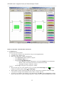
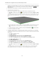
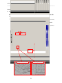
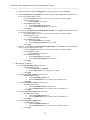
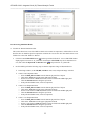
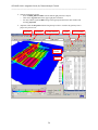
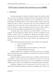
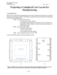
CFD-ACE+ 2003 : Integrated Circuit (IC) Thermal Analysis Tutorial
____________________________________________________________________________________
CFD-ACE+
Version 2003
Micromesh/Heat Tutorial
10-03
Integrated Circuit (IC)
Thermal Analysis
• Building a 3D simulation model of an integrated circuit (IC) from a layout
using CFD-Micromesh
• Setting up a Heat Transfer simulation in CFD-ACE+
• Steady-state simulation with surface heat sources
• Post-processing using CFD-VIEW
CFD Research Corporation
Cummings Research Park
215 Wynn Drive, Suite 501, Huntsville, AL 35805
Phone: (256) 726- 4800, Fax: (256) 726- 4806
Software Support: [email protected], Phone: (256) 726- 4900
Sales: [email protected], www.cfdrc.com
© 2003 by CFD Research Corporation
All rights reserved.
1
CFD-ACE+ 2003 : Integrated Circuit (IC) Thermal Analysis Tutorial
____________________________________________________________________________________
Tutorial:
Integrated Circuit (IC) Thermal Analysis
PAGE
GENERAL INFORMATION
Problem Description and Objectvies .
.
.
.
.
.
3
Importing Layout and Defining Technology .
.
.
Set Model Gometry Dimensions and Grid Step
.
.
Generate/Edit Process Sequence
.
.
.
.
Edit Layer Operation, Vertical Position, and Layout .
.
Save Micromesh Project and Technology Files
.
.
Generating and Viewing 3D Solid Model .
.
.
Automatic Generation of 3D Computational Mesh .
.
Viewing the Generated 3D Computational Mesh (DTF file) .
Setting Up A Thermal Simulation in CFD-ACE+ .
.
Post-Processing Simulation Results .
.
.
.
.
.
.
.
.
.
.
.
.
.
.
.
.
.
.
.
.
.
.
.
4
5
5
5
5
5
5
6
6
6
.
.
.
.
.
.
.
.
.
.
.
.
.
.
.
.
.
.
.
.
7
9
10
13
17
17
19
21
22
25
CONDENSED TUTORIAL
DETAILED TUTORIAL
Importing Layout and Defining Technology .
.
.
Set Model Gometry Dimensions and Grid Step
.
.
Generate/Edit Process Sequence
.
.
.
.
Edit Layer Operation, Vertical Position, and Layout .
.
Save Micromesh Project and Technology Files
.
.
Generating and Viewing 3D Solid Model .
.
.
Automatic Generation of 3D Computational Mesh .
.
Viewing the Generated 3D Computational Mesh (DTF file) .
Setting Up A Thermal Simulation in CFD-ACE+ .
.
Post-Processing Simulation Results .
.
.
.
2
CFD-ACE+ 2003 : Integrated Circuit (IC) Thermal Analysis Tutorial
____________________________________________________________________________________
PROBLEM DESCRIPTION AND OBJECTIVES
Perform thermal analysis of integrated circuit (IC), starting from original electronic layout and process information.
Electronic integrated circuit (IC) designs are very often stored in the form of layout (top view) of all the layers
composing the design. Similar method is used to store and transfer designs of electronic printed-circuit boards
(PCBs), multi-chip modules (MCMs), and micro-electro-mechanical systems (MEMS). To perform a physical
simulation of such structures we need to create a 3D computational mesh from the layout, using additional
information about particular layer properties (position, thickness, material). The latter information is also called
process data, and may be stored as a technology file.
In this tutorial we show how to:
- import a layout from a CIF file
- define the process data (properties of layers), and save as a Technology File
(which can be used for subsequent fast and automatic building of models from different layouts of the same
technological process)
- create and view interactively a 3D model
- generate three-dimensional (3D) mesh
- setup and perform thermal simulation
- visualize thermal results of simulation
As an example, we use an IC device as illustrated in Figure 1. Heat sources present in the silicon device layer of the
3D model are modeled as 2D surface heat sources located exactly at the top surface of the silicon, which
corresponds to the location of CMOS transistor channels. The heat sources are located in four groups (inverter
clusters), as illustrated in Figure 2. Sample calculated temperature distributions are can also be seen in Figure 2.
Figure 1. IC layout in CFD-Micromesh (left) and a three-dimensional solid model built automatically in CFDMicromesh (right).
Figure 2. Location of inverter-clusters used as separate heat sources in the IC thermal model (left) and calculated
temperature distribution when all heat source groups (A–D) active (right).
3
CFD-ACE+ 2003 : Integrated Circuit (IC) Thermal Analysis Tutorial
____________________________________________________________________________________
CONDENSED TUTORIAL
The following is a summary of the steps in this tutorial. Detailed explanations of each step follows the summary.
This summary can be useful for users who are somewhat familiar with the software and the overall process of setting
up and running an IC thermal simulation. The summary shown below matches the detailed description which
follows, hence allowing the user to use the summary description below and detailed explanations for steps which
may be unfamiliar to the user.
Importing Layout and Defining Technology
1.
Import the IC CIF layout file: “IC_Heat.cif” with no technology file
a.
Obtain layer names from CIF file in text editor:
Layer
Layer
Layer
Layer
Layer
Layer
b.
nwell = CIF Layer CWN
Layer
nselect = CIF Layer CSN
Layer
pselect = CIF Layer CSP
Layer
active = CIF Layer CAA
Layer
active contact = CIF Layer CCA Layer
poly = CIF Layer CPG
Layer
polycontact = CIF Layer CCP
m1m2 contact = CIF Layer CVA
pad = CIF Layer CMP
metal1 = CIF Layer CMF
metal2 = CIF Layer CMS
glass = CIF Layer CFI
Obtain vertical dimensions and material composition.
2.
Explore and understand CFD-Micromesh environment
3.
Convert CIF layer names into physical layer names (using information from step 1a).
CWN
Rename to: “nwell”,
CSN
Rename to: “nselect”,
CSP
Rename to: “pselect”,
etc. ... (Note that physical layers “pad” and “glass” are not present in the layout)
4
CFD-ACE+ 2003 : Integrated Circuit (IC) Thermal Analysis Tutorial
____________________________________________________________________________________
Set Model Gometry Dimensions and Grid Step
4.
Set model geometry boundary dimensions (min, max, voxel size) [um]:
X(0, 100, 0.16), Y(0, 100, 0.16), Z(-1, 5, 0.01)
5.
Set size of grid step used in Micromesh for drawing layouts to 1.0 um.
Generate/Edit Process Sequence
6.
Removal of unnecessary process layers. The following layers may be removed: active, poly contact, poly,
nselect, pselect, and nwell
7.
Ordering of remaining process layers. For the remaining 4 layers, active contact should be on the bottom, with
metal1 above, then m1m2 above, and finally metal2 on top.
8.
Generate missing process layers. The following layers (and hence, material names) must be added to the
process: Bottom, Bulk_Silicon, Oxide, HeatA, HeatB, HeatC, HeatD, Semi_Device
9.
Ordering of process layers. The final ordering should be as follows, from bottom to top: Bottom
Bulk_Silicon Oxide Semi_Device HeatA HeatB HeatC HeatD Active_Contact
M1M2 Metal2
Metal1
Edit Layer Operation, Vertical Position, and Layout (all units in micrometers)
10.
11.
12.
13.
14.
15.
16.
17.
18.
19.
20.
21.
layer: Bottom
deposit (no mesh)1.0 thick
layer: Bulk_Silicon deposit
0.5 thick
layer: Oxide
deposit
4.5 thick
layer: Semi_Device insert
position 0.7, 0.05 thick
layer: HeatA
insert
position 0.75, 0.15 thick
layer: HeatB
insert
position 0.75, 0.15 thick
layer: HeatC
insert
position 0.75, 0.15 thick
layer: HeatD
insert
position 0.75, 0.15 thick
(22.56, 44.0) to (42.56, 63.0) : (44.0, 44.0) to (64.0, 63.0)
layer: Active_Contact insert
position 0.75, 0.8 thick
layer: Metal1
insert
position 1.55, 0.65 thick
layer: M1M2
insert
position 2.2, 1.0 thick
layer: Metal2
insert
position 3.2, 0.65 thick
rectangle: (0, 0) to (100, 100)
rectangle: (0, 0) to (100 ,100)
rectangle: (0, 0) to (100, 100)
rectangle: (22.24, 22.4) to (85.92, 64.0)
rectangle: (70.56, 23.36) to (85.76, 42.4)
rectangle: (65.76, 23.36) to (70.4, 42.4)
rectangle: (44.0, 23.36) to (64.0, 42.4)
rectangles: (22.56, 23.52) to (42.56, 42.52) :
: (65.4, 44.0) to (85.4, 63.0)
remove rectangles present in four corners
remove rectangles present in four corners
remove rectangles present in four corners
remove rectangles present in four corners
Save Micromesh Project and Technology Files
22. Save Micromesh Technology file
23. Save Micromesh project file
: File
: File
Save Technology … “IC_Heat.umt”
Save Project As … “IC_Heat.ump”
Generating and Viewing 3D Solid Model
24. Viewing model with 3D quick view. View entire structure or internal components by making layers Oxide and
Bulk_Silicon non-meshed.
Automatic Generation of 3D Computational Mesh
25. Add mesh cell size layer to process. Set Mesh Cells Size to 10. Draw rectangles with coordinates:
(0, 0) to (20.6, 100) ; (87.7, 0) to (100, 100) ; (0, 0) to (100.0, 22) ; (0, 65) to (100, 100)
26. Build 3D Prism-Hexa unstructured computational grid. Select “Old prisms-hexahedra mesh (before version
2002)” and set to 25,000 triangles, 1000000 initial z size cell, 6E-6 Z direction threshold, 1 smoothness
5
CFD-ACE+ 2003 : Integrated Circuit (IC) Thermal Analysis Tutorial
____________________________________________________________________________________
tolerance, no Z mesh, “default” mesh
Results in ~145,000 prism and ~41,000 hexa cells are generated, hence
~186,000 total computational cells for the geometry.
Viewing the Generated 3D Computational Mesh (DTF file)
27. View 3D computational mesh in CFD-VIEW.
Setting Up A Thermal Simulation in CFD-ACE+
28. Open DTF file in CFD-GUI
29. Setup steady simulation for the IC geometry.
PT: Heat
MO: Steady
VC: Properties
Bulk_Silicon, Semi_Device
Density 2300, Specific Heat 700, Therm Conductivity 155
Oxide, HeatA, HeatB, HeatC, HeatD
Density 2150, Specific Heat 740, Therm Conductivity 1.3
Active_Contact, Metal1, M1M2, Metal2
Density 2700, Specific Heat 938, Therm Conductivity 230
BC: Bottom_Bulk_Silicon Isothermal 300K
Semi_Device_HeatA Wall Heat Source at 39045 W/m^2
Semi_Device_HeatB Wall Heat Source at 513865 W/m^2
Semi_Device_HeatC Wall Heat Source at 477895 W/m^2
Semi_Device_HeatD Wall Heat Source at 740131.6 W/m^2
IC: default
SC: Max Iterations 30, Enthalpy AMG Solver, Enthalpy Relaxation 1E-13
OUT: Static Temperature and Wall Heat Flux
File Save (saves file “IC_Heat.DTF”)
30. Run the IC thermal simulation.
Post-Processing Simulation Results
31. Visualize IC thermal simulation results
6
CFD-ACE+ 2003 : Integrated Circuit (IC) Thermal Analysis Tutorial
____________________________________________________________________________________
DETAILED TUTORIAL
In the following lesson these definitions apply:
LB = Left mouse button, MB = Middle mouse button, RB = Right mouse button
Importing Layout and Defining Technology
1.
Import the IC CIF layout. From the File pull down menu, select: Import
CIF file ...
A window appears with the question: "Do you want to select technology file?” At this point, we don’t yet have
a technology file defined for this project, thus answer No to the question.
In the "Import CIF Project" window, select the file you want (for this tutorial “IC_Heat.cif”), and click OK.
A layout of the device appears in the "Layout" editing window (shown above), with the layer names coming
from the original CIF file. Typically, the layers defined in a CIF file can not be used directly for automatic
building of 3D computational models within CFD-Micromesh. Therefore, a special technology file is needed for
mapping the layers from a CIF file into physical layers, and a special sequence of operations performed by
CFD-Micromesh needs to be defined. A Micromesh Technology File (with extension .umt) can be used for
subsequent fast and automatic building of models from different layouts of the same technological process.
In this tutorial we will create such a technology file manually from information provided along with the CIF
layout file. In this IC case, we have the following additional technology information available:
Layer names:
As was seen from the imported CIF file in Micromesh, the coded CIF layer names available are non-descriptive
and of little use. Knowledge of what each layer is in the process is required for proper model development.
Hence, the coded CIF layer names need to be converted into physical layer names.
The easiest way to determine the layer name conversion information is to open the CIF file in a text editor.
Near the beginning of the file, comments might be present mapping the layer names with the CIF layer names.
Whether this information is present or not depends on the layout tool used to generate the CIF file. If this
information is not available in the CIF file, direct knowledge of the layer name mapping must be obtained from
the CIF layout author.
7
CFD-ACE+ 2003 : Integrated Circuit (IC) Thermal Analysis Tutorial
____________________________________________________________________________________
For this tutorial case, the following information was present in the CIF file, mapping the layer names as shown
below:
Layer
Layer
Layer
Layer
Layer
Layer
Layer
Layer
Layer
Layer
Layer
Layer
nwell = CIF Layer CWN
nselect = CIF Layer CSN
pselect = CIF Layer CSP
active = CIF Layer CAA
active contact = CIF Layer CCA
poly = CIF Layer CPG
polycontact = CIF Layer CCP
m1m2 contact = CIF Layer CVA
pad = CIF Layer CMP
metal1 = CIF Layer CMF
metal2 = CIF Layer CMS
glass = CIF Layer CFI
Vertical Dimensions and Material Composition:
To build a 3D model from layout, we need also an information about the “3rd dimension” of the structure, that is
vertical dimensions of particular layers in the layout, and their material composition. This information must be
obtained from some source. For this IC case, this information is illustrated in Figure 3 below.
Figure 3. Vertical dimensions of layers in the chip structure, and their material composition.
8
CFD-ACE+ 2003 : Integrated Circuit (IC) Thermal Analysis Tutorial
____________________________________________________________________________________
2.
If the user is unfamiliar with the Micromesh environment, explore the layout editing window.
•
•
•
•
•
•
•
•
•
•
3.
The mouse buttons work as in the other CFDRC software: LB is used to select an object, MB - to zoom in
and out the view, RB - to shift (pan) the view. A context-sensitive help is in the lower-left corner of the
main window.
Note also the current coordinates (X, Y) of the cursor on the screen, appearing in the lower-right corner of
the main window. Initially, the units are set automatically according to the size of the imported file
(micrometers in this case), but you can change them (menu: View -> Display Units).
On the right side of the main window, examine all layers constituting your project.
Starting from the most bottom layer (GDS_31 in this example), keep clicking LB on subsequent higher
layers, to see them appearing sequentially in the layout.
Objects belonging to the selected layer are highlighted in the layout.
Note that by default only the layers below the currently active layer are displayed.
By clicking RB on the highlighted layer name (in the right window), you can view and/or change properties
of this layer. The change will affect all the objects belonging to this layer.
By clicking LB on an element of layout of the highlighted layer (left part of the window), you can select
the specific element in this layer, then move it, stretch, copy, delete, etc.
By clicking RB on the selected element of layout, you can view and/or change properties of the particular
element. The change will affect only this object.
Explore the icon buttons at the top of main window, and their description, by hovering the mouse cursor
(without clicking) for a while on each button. A longer explanation of the button function appears also in
the bottom-left corner of the main window.
Convert CIF layer names into physical layer names, using the technology information presented previously (as
obtained from the CIF file as viewed in a text editor).
•
•
•
•
•
•
Select (by clicking LB) the first layer at the bottom of the list (in this case: CAA).
Click RB on the selected layer name
- the “Layer Properties” dialog window opens.
Select Edit Material button - the “Materials” dialog window opens
Change the CIF “material” names into new (physical) names, by clicking on Rename button in the
"Materials" window. For example:
CWN
Rename to: “nwell”,
CSN
Rename to: “nselect”,
CSP
Rename to: “pselect”,
etc. ...
Note that physical layers “pad” and “glass” are not present in the layout.
Click Close in the "Materials" window.
Click Accept in the "Layer Properties" window.
Set Model Geometry Dimensions and Grid Step
4.
On the basis of the technology (process) description presented in Figure 3 (vertical information), we can now
set up the project vertical boundaries at Zmin = -1.0 µm, Zmax = 5.0 µm, and a voxel size to 0.01 µm. At this
time, the X and Y range will also be adjusted slightly as shown in the image below.
•
From the toolbar, click the Change Boundary button [
].
The "Dimensions and Resolutions" dialog window opens. Change the values of the fields to match the
values shown below. Note that voxel size is expressed in voxels, or three-dimensional blocks, analogous to
two-dimensional pixels in 2D images. The largest voxel size should be chosen that can still capture the
dimensions of the elements (or smallest grid element you would like to have). Hence, noting the smallest
element resolution in your geometry, including any overlaping elements, is key to allow for the largest
voxel size but reduce the required memory allocation for grid generation. For this tutorial, voxel sizes of
9
CFD-ACE+ 2003 : Integrated Circuit (IC) Thermal Analysis Tutorial
____________________________________________________________________________________
0.16 um for the X and Y direction are appropriate. In the Z direction, a voxel size of 0.1 um is chosen to
allow for multiple grid cells in the smaller layers if desired (smallest layer thickness is 0.5 um).
•
5.
Click the Accept button.
Change size of grid used in Micromesh for drawing layouts.
The size of grid step may be changed in Micromesh. This grid is useful in snap-to-grid drawing of 2D layouts.
While the grid may not allow for the exact desired dimensions, this smaller grid step will allow for near-exact
drawing of layouts. By then editing the drawn layout element, final exact location/dimensions of the elements
may be accomplished (RB click on drawn element and edit).
•
•
•
From the toolbar, click the Change Grid button [ ].
The "Grid" dialog window opens. Change the value of the field Grid Step [um]: to 1.0
Click the Accept button.
Generate/Edit Process Sequence
6.
Removal of Unnecessary Process Layers
The layout information imported from the CIF layout file contains much detailed information that is not going
to be used in this simulation. Specifically, information regarding the manufacturing of the semiconductor
devices. For the simulation, a single block layer will be used to represent the silicon semiconductor device
layer instead of the multiple layers present in the CIF file. This single layer will be added later, therefore, we
may now remove these unnecessary layers from the layout.
The layers which may be removed from the layout include: active, poly contact, poly, nselect, pselect, and
nwell.
7.
•
To remove a layer, click LB on the layer name displayed in the Layer List. Next click on the Delete Layer
•
button [ ]. The layer has now been deleted.
Delete the 6 layers as listed above (active, poly contact, poly, nselect, pselect, and nwell)
Ordering of Remaining Process Layers
Model building operations in CFD-Micromesh are performed in the order in which they are displayed in the
Layer List on the right-hand side of the main window. The layer displayed at the bottom of the list is inserted
into the model first; the others follow in order from the bottom to the top of the list. This is similar to the layers
that are processed (deposited, diffused, etched, etc.) one after another, as in the microelectronics manufacturing
process.
On the basis of Figure 3 (vertical description), rearrange the remaining layers into the correct sequence in
the layer list. For the remaining 4 layers, active contact should be on the bottom, with metal1 above, then
m1m2 above, and finally metal2 on top. The order currently is nearly correct, with only the m1m2 layer
needing to be lowered one position in the Layer List. To rearrange:
• select “m1m2” layer in the list,
10
CFD-ACE+ 2003 : Integrated Circuit (IC) Thermal Analysis Tutorial
____________________________________________________________________________________
•
while holding LB, drag the “m1m2” layer name down so that it is between the metal2 and metal1
layers, then releasing the LB
The four layers should now be arranged correctly.
8.
Generate Missing Process Layers
If you compare the current layer now with Figure 3, you notice that there are several process layers missing in
the layout (Bottom, Bulk_Silicon, Oxide, HeatA, HeatB, HeatC, HeatD, Semi_Device). To build a complete
model, we need to add manually those missing layers to our process description in CFD-Micromesh.
Before adding the new layers though, let us add the desired layer name materials to the material list. This
can be done by clicking the pull-down menu Tools Edit Materials…
• Since we want to create new layers with different names, click the Add button in the "Materials"
window.
• In the "New Material" window, type the name “Bottom" and click Accept
• Again click the Add button in the "Materials" window
• In the "New Material" window, type the name “Bulk_Silicon" and click Accept
• Repeat this process to add the remaining desired materials: Oxide, HeatA, HeatB, HeatC, HeatD, and
Semi_Device
• Click Close in the "Materials" window.
To add a new “Bottom” layer:
• click LB on the top Layer metal2 in the Layer List
•
•
•
•
button in the top toolbar. In the list of layers on the right-hand side,
click LB the New Layer
you should see a new layer with the name "NEW: metal2 (deposit)" (creating a new layer makes a
copy of the currently active layer with all its properties).
In the list of layers, click RB on the "NEW: metal2 (deposit)" layer.
In the "Layer Properties" window which appears, change the Material pull-down selection to
“Bottom”
click Accept
To add a new “Bulk_Silicon” layer:
•
•
•
•
button in the top toolbar. In the list of layers on the right-hand side,
click LB the New Layer
you should see a new layer with the name "NEW: Bottom (deposit)"
In the list of layers, click RB on the "NEW: Bottom (deposit)" layer.
In the "Layer Properties" window which appears, change the Material pull-down selection to
“Bulk_Silicon”
click Accept
To add a new “Oxide” layer:
•
•
•
•
button in the top toolbar. In the list of layers on the right-hand side,
click LB the New Layer
you should see a new layer with the name "NEW: Bulk_Silicon (deposit)"
In the list of layers, click RB on the "NEW: Bulk_Silicon (deposit)" layer.
In the "Layer Properties" window which appears, change the Material pull-down selection to “Oxide”
click Accept
To add a new “HeatA” layer:
•
•
•
button in the top toolbar. In the list of layers on the right-hand side,
click LB the New Layer
you should see a new layer with the name "NEW: Oxide (deposit)"
In the list of layers, click RB on the "NEW: Oxide (deposit)" layer.
In the "Layer Properties" window which appears, change the Material pull-down selection to “HeatA”
11
CFD-ACE+ 2003 : Integrated Circuit (IC) Thermal Analysis Tutorial
____________________________________________________________________________________
•
click Accept
To add a new “HeatB” layer:
•
•
•
•
click LB the New Layer
button in the top toolbar. In the list of layers on the right-hand side,
you should see a new layer with the name "NEW: HeatA (deposit)"
In the list of layers, click RB on the "NEW: HeatA (deposit)" layer.
In the "Layer Properties" window which appears, change the Material pull-down selection to “HeatB”
click Accept
To add a new “HeatC” layer:
•
•
•
•
button in the top toolbar. In the list of layers on the right-hand side,
click LB the New Layer
you should see a new layer with the name "NEW: HeatB (deposit)"
In the list of layers, click RB on the "NEW: HeatB (deposit)" layer.
In the "Layer Properties" window which appears, change the Material pull-down selection to “HeatC”
click Accept
To add a new “HeatD” layer:
•
•
•
•
button in the top toolbar. In the list of layers on the right-hand side,
click LB the New Layer
you should see a new layer with the name "NEW: HeatC (deposit)"
In the list of layers, click RB on the "NEW: HeatC (deposit)" layer.
In the "Layer Properties" window which appears, change the Material pull-down selection to “HeatD”
click Accept
To add a new “Semi_Device” layer:
•
•
•
•
9.
button in the top toolbar. In the list of layers on the right-hand side,
click LB the New Layer
you should see a new layer with the name "NEW: HeatD (deposit)"
In the list of layers, click RB on the "NEW: HeatD (deposit)" layer.
In the "Layer Properties" window which appears, change the Material pull-down selection to
“Semi_Device”
click Accept
Ordering of Process Layers
All the required process layers are now present in the layout, but the newly added layers need to be moved to
appropriate positions in the list. Therefore, based on Figure 3, the process layers should be reorganized. Figure
4 illustrates the order of the layers before and after re-ordering. The left image illustrates the ordering before
rearranging, and the right image illustrates the final ordering required. The final ordering should be as follows,
from bottom to top: Bottom Bulk_Silicon Oxide Semi_Device HeatA HeatB HeatC HeatD
Active_Contact Metal1 M1M2 Metal2
12
CFD-ACE+ 2003 : Integrated Circuit (IC) Thermal Analysis Tutorial
____________________________________________________________________________________
Figure 4. Layer process order before (left) and after (right) re-ordering.
Edit Layer Operation, Vertical Position, and Layout
10. Edit Bottom layer:
Operation and vertical position:
• Click LB on the “Bottom” layer from the list of layers on the right-hand side
• Click RB on the “Bottom” layer
• In the “Layer Properties” window which appears:
o set the Operation: pull-down menu to “deposit”
o set the Thickness [um]: to 1.0
o click LB on the Edit Material button
in the “Materials” window which appears, un-check the Mesh It box for the material
“Bottom” (hence, this material will not be be meshed in the model)
click Close, closing the “Materials” window
o click Accept, closing the “Layer Properties” window
Layout:
• Draw a layout (top view) of the “Bottom” layer, by selecting the New Rectangle button [ ] from the
toolbar (or from the top menu: Tools New Rectangle).
• While holding left mouse button down and observing the current cursor coordinates in the lower-right
corner, draw a rectangle with coordinates (0 um, 0 um) to (100 um, 100 um).
• To check if your “Bottom” layout has the correct dimensions, click RB on the red (highlighted) rectangle
that you have just drawn. In the “Rectangle Properties” window check if position and dimensions of your
13
CFD-ACE+ 2003 : Integrated Circuit (IC) Thermal Analysis Tutorial
____________________________________________________________________________________
rectangle are appropriate. If not, correct them by typing the accurate number (Pos.X = 0, Pos.Y = 0, Size X
= 100, Size Y = 100), and click Accept.
11. Edit Bulk_Silicon layer:
Operation and vertical position:
• Click LB on the “Bulk_Silicon” layer from the list of layers on the right-hand side
• Click RB on the “Bulk_Silicon” layer
• In the “Layer Properties” window which appears:
o set the Operation: pull-down menu to “deposit”
o set the Thickness [um]: to 0.5
o click Accept
Layout:
• Draw a layout (top view) of the “Bulk_Silicon” layer, by selecting the New Rectangle button [ ]
• Draw a rectangle with coordinates (0 um, 0 um) to (100 um, 100 um).
• To check dimensions, click RB on the red (highlighted) rectangle: correct values should be (Pos.X = 0,
Pos.Y = 0, Size X = 100, Size Y = 100)
12. Edit Oxide layer:
Operation and vertical position:
• Click LB on the “Oxide” layer from the list of layers on the right-hand side
• Click RB on the “Oxide” layer
• In the “Layer Properties” window which appears:
o set the Operation: pull-down menu to “deposit”
o set the Thickness [um]: to 4.5
o click Accept, closing the “Layer Properties” window
Layout:
• Draw a layout (top view) of the “Oxide” layer, by selecting the New Rectangle button [ ]
• Draw a rectangle with coordinates (0 um, 0 um) to (100 um, 100 um).
• To check dimensions, click RB on the red (highlighted) rectangle: correct values should be (Pos.X = 0,
Pos.Y = 0, Size X = 100, Size Y = 100)
13. Edit Semi_Device layer:
Operation and vertical position:
• Click LB on the “Semi_Device” layer from the list of layers on the right-hand side
• Click RB on the “Semi_Device” layer
• In the “Layer Properties” window which appears:
o set the Operation: pull-down menu to “insert”
o set the Position [um]: to 0.7
o set the Thickness [um]: to 0.05
o click Accept, closing the “Layer Properties” window
Layout:
• Draw a layout (top view) of the “Semi_Device” layer, by selecting the New Rectangle button [ ]
• Draw a rectangle with coordinates (22.24 um, 22.4 um) to (85.92 um, 64 um).
• To check dimensions, click RB on the red (highlighted) rectangle: correct values should be (Pos.X =
22.24, Pos.Y = 22.4, Size X = 63.68, Size Y = 41.6)
14. Edit HeatA layer:
Operation and vertical position:
• Click LB on the “HeatA” layer from the list of layers on the right-hand side
• Click RB on the “HeatA” layer
• In the “Layer Properties” window which appears:
o set the Operation: pull-down menu to “insert”
o set the Position [um]: to 0.75
o set the Thickness [um]: to 0.15
14
CFD-ACE+ 2003 : Integrated Circuit (IC) Thermal Analysis Tutorial
____________________________________________________________________________________
o click Accept, closing the “Layer Properties” window
Layout:
• Draw a layout (top view) of the “HeatA” layer, by selecting the New Rectangle button [ ]
• Draw a rectangle with coordinates (70.56 um, 23.36 um) to (85.76 um, 42.4 um).
• To check dimensions, click RB on the red (highlighted) rectangle: correct values should be (Pos.X =
70.56, Pos.Y = 23.36, Size X = 15.2, Size Y = 19.04)
15. Edit HeatB layer:
Operation and vertical position:
• Click LB on the “HeatB” layer from the list of layers on the right-hand side
• Click RB on the “HeatB” layer
• In the “Layer Properties” window which appears:
o set the Operation: pull-down menu to “insert”
o set the Position [um]: to 0.75
o set the Thickness [um]: to 0.15
o click Accept, closing the “Layer Properties” window
Layout:
• Draw a layout (top view) of the “HeatB” layer, by selecting the New Rectangle button [ ]
• Draw a rectangle with coordinates (65.76 um, 23.36 um) to (70.4 um, 42.4 um).
• To check dimensions, click RB on the red (highlighted) rectangle: correct values should be (Pos.X =
65.76, Pos.Y = 23.36, Size X = 4.64, Size Y = 19.04)
16. Edit HeatC layer:
Operation and vertical position:
• Click LB on the “HeatC” layer from the list of layers on the right-hand side
• Click RB on the “HeatC” layer
• In the “Layer Properties” window which appears:
o set the Operation: pull-down menu to “insert”
o set the Position [um]: to 0.75
o set the Thickness [um]: to 0.15
o click Accept, closing the “Layer Properties” window
Layout:
• Draw a layout (top view) of the “HeatC” layer, by selecting the New Rectangle button [ ]
• Draw a rectangle with coordinates (44.0 um, 23.36 um) to (64.0 um, 42.4 um).
• To check dimensions, click RB on the red (highlighted) rectangle: correct values should be (Pos.X = 44.0,
Pos.Y = 23.36, Size X = 20.0, Size Y = 19.04)
17. Edit HeatD layer:
Operation and vertical position:
• Click LB on the “HeatD” layer from the list of layers on the right-hand side
• Click RB on the “HeatD” layer
• In the “Layer Properties” window which appears:
o set the Operation: pull-down menu to “insert”
o set the Position [um]: to 0.75
o set the Thickness [um]: to 0.15
o click Accept, closing the “Layer Properties” window
Layout:
• Draw a layout (top view) of the “HeatD” layer, which includes four rectangles
• Draw first rectangle by selecting the New Rectangle button [ ]
o Draw a rectangle with coordinates (22.56 um, 23.52 um) to (42.56 um, 42.52 um).
o To check dimensions, click RB on the red (highlighted) rectangle: correct values should be
(Pos.X = 22.56, Pos.Y = 23.52, Size X = 20.0, Size Y = 19.0)
• Draw second rectangle by selecting the New Rectangle button [ ]
o Draw a rectangle with coordinates (22.56 um, 44.0 um) to (42.56 um, 63.0 um).
15
CFD-ACE+ 2003 : Integrated Circuit (IC) Thermal Analysis Tutorial
____________________________________________________________________________________
To check dimensions, click RB on the red (highlighted) rectangle: correct values should be
(Pos.X = 22.56, Pos.Y = 44.0, Size X = 20.0, Size Y = 19.0)
Draw third rectangle by selecting the New Rectangle button [ ]
o Draw a rectangle with coordinates (44.0 um, 44.0 um) to (64.0 um, 63.0 um).
o To check dimensions, click RB on the red (highlighted) rectangle: correct values should be
(Pos.X = 44.0, Pos.Y = 44.0, Size X = 20.0, Size Y = 19.0)
Draw fourth rectangle by selecting the New Rectangle button [ ]
o Draw a rectangle with coordinates (65.4 um, 44.0 um) to (85.4 um, 63.0 um).
o To check dimensions, click RB on the red (highlighted) rectangle: correct values should be
(Pos.X = 65.4, Pos.Y = 44.0, Size X = 20.0, Size Y = 19.0)
o
•
•
18. Edit Active_Contact layer:
Operation and vertical position:
• Click LB on the “Active_Contact” layer from the list of layers on the right-hand side
• Click RB on the “Active_Contact” layer
• In the “Layer Properties” window which appears:
o set the Operation: pull-down menu to “insert”
o set the Position [um]: to 0.75
o set the Thickness [um]: to 0.8
o click Accept, closing the “Layer Properties” window
Layout:
• The layout for this layer already exists, though some clean-up is of use. Specifically, there are elements of
the contacts in the four corners of the model which are not needed.
• These elements may be deleted by highlighting them and hitting the delete button on your keyboard
• To highlight these elements, simply click LB near the elements and drag and hold the mouse to create a
square enclosing the elements. The highlighted elements will appear in red. Simply hit delete to remove
these elements.
19. Edit Metal1 layer:
Operation and vertical position:
• Click LB on the “Metal1” layer from the list of layers on the right-hand side
• Click RB on the “Metal1” layer
• In the “Layer Properties” window which appears:
o set the Operation: pull-down menu to “insert”
o set the Position [um]: to 1.55
o set the Thickness [um]: to 0.65
o click Accept, closing the “Layer Properties” window
Layout:
• The layout for this layer already exists, though some clean-up is of use. Specifically, there are elements of
the contacts in the four corners of the model which are not needed.
• These elements may be deleted by highlighting them and hitting the delete button on your keyboard
20. Edit M1M2 layer:
Operation and vertical position:
• Click LB on the “M1M2” layer from the list of layers on the right-hand side
• Click RB on the “M1M2” layer
• In the “Layer Properties” window which appears:
o set the Operation: pull-down menu to “insert”
o set the Position [um]: to 2.2
o set the Thickness [um]: to 1.0
o click Accept, closing the “Layer Properties” window
Layout:
• The layout for this layer already exists, though some clean-up is of use. Specifically, there are elements of
the contacts in the four corners of the model which are not needed.
• These elements may be deleted by highlighting them and hitting the delete button on your keyboard
16
CFD-ACE+ 2003 : Integrated Circuit (IC) Thermal Analysis Tutorial
____________________________________________________________________________________
21. Edit Metal2 layer:
Operation and vertical position:
• Click LB on the “Metal2” layer from the list of layers on the right-hand side
• Click RB on the “Metal2” layer
• In the “Layer Properties” window which appears:
o set the Operation: pull-down menu to “insert”
o set the Position [um]: to 3.2
o set the Thickness [um]: to 0.65
o click Accept, closing the “Layer Properties” window
Layout:
• The layout for this layer already exists, though some clean-up is of use. Specifically, there are elements of
the contacts in the four corners of the model which are not needed.
• These elements may be deleted by highlighting them and hitting the delete button on your keyboard
Save Micromesh Project and Technology Files
22. Save your current settings as a Micromesh Technology File:
• Click File Save Technology from the top menu.
The Save Technology window opens up.
• In File name, type “IC_Heat.umt” as the name of the file, and click OK.
Micromesh Technology File is saved with extension .umt (for µMesh Technology).This file can be used later for
fast and automatic building of 3D models and meshes from different layouts imported from GDSII or CIF files,
associated with the same technological process.
In such a case, click Yes in the Technology File window appearing during importing GDSII or CIF layout, and
select the saved Micromesh Technology File (.umt)
23. At this point, you may save your existing Micromesh project to a disk file, to secure the work you have done so
far. Projects in CFD-Micromesh are saved to disk in a special format, containing all model data as well as setup
parameters for the 3D model and mesh generation for the current project. All these data are saved to a binary
disk file with extension .ump (for µMesh Project).
• From the toolbar, click Save . The “Save Project As” dialog opens.
• In File name, type “IC_Heat.ump” as the name of the file, and click OK.
Generating and Viewing 3D Solid Model
24. There are three methods of generating and viewing a 3D model in CFD-Micromesh:
•
•
•
3D Quick View – Very fast building of a 3D model from planar elements of defined position and
thickness, and viewing the 3D model with zooming and rotation. This option is limited to layouts including
rectangular shapes only. Non-rectangular shapes will appear as rectangular in any 3D quick view
representation. Typical model building time: 1-2 seconds (700 MHz Pentium PC).
3D Solid View – Generating a solid model by geometrical deposition/etching simulation, using voxel
(volumetric pixel) technology – this technique allows to generate models of arbitrary shapes, including
rounded and oblique side-walls, non-planar conformal layers, etc. Viewing the 3D model allows for
zooming and rotation. Typical model building time: 1-5 minutes (700 MHz Pentium PC).
3D Photo - Generating a solid model by geometrical deposition/etching simulation, using voxel technology
(the same as in method 2) – this technique allows to generate models of arbitrary shapes, like rounded side
walls, non-planar layers, etc. Visualization procedure uses the ray tracing technique that produces up to
four different static views (stored as GIF files) of the generated 3D model. Though these are only static
17
CFD-ACE+ 2003 : Integrated Circuit (IC) Thermal Analysis Tutorial
____________________________________________________________________________________
•
•
snapshots of the 3D model, thanks to ray tracing, they give the highest quality of rendering, with controlled
light, shadows, reflections, and anti-aliasing. Typical model and pictures building time: 3-10 minutes (700
MHz Pentium PC).
Each of the above three methods is activated by a separate button in the top toolbar:
Using the first option “3D Quick View”:
We will use the “3D Quick View” option since our model consists of rectangular sections only.
Click LB on "3D Quick View" button [ ] in the top toolbar (or from top menu: Compute -> Quick
View).
A new window appears, and it shows the quick view model, similar to below. Note that all that can be seen
is the deposited Oxide and Bulk_Silicon. The other layers are internal to the geometry and are not visible
here.
In the “3D Quick View” window, use LB - to rotate the model, MB - to zoom in and out the view and
RB - to shift (pan) the view. Hover the cursor over different layers in the structure to see the layer
name.
Scaling of the model, if desired, is available by clicking the Scale Solid button [
Close the “3D Quick View” window.
•
] in the top toolbar
Viewing the “internal” structure, i.e. interconnects (metal1, metal2), vias, heat sources, etc. This will be
accomplished by making the Oxide and Bulk_Silicon layers non-visible by temporarily turning off meshing
of these layers.
Click LB on the Oxide layer name.
Click RB on Oxide layer
In the Layer Properties window which opens, click on Edit Material button
In the Materials window which opens, uncheck the Mesh It box for Oxide
Click Close, in the Materials window and click Accept in the Layer Properties window
Click LB on the Bulk_Silicon layer name.
Click RB on Bulk_Silicon layer
In the Layer Properties window which opens, click on Edit Material button
In the Materials window which opens, uncheck the Mesh It box for Bulk_Silicon
Click Close, in the Materials window and click Accept in the Layer Properties window
Click LB on "3D Quick View" button [ ] in the top toolbar (or from top menu: Compute Quick
View).
A new window appears, and it shows the quick view model, similar to below. Note that the deposited
Oxide and Bulk_Silicon layers are no longer seen. Now, the remaining internal layers are visible.
18
CFD-ACE+ 2003 : Integrated Circuit (IC) Thermal Analysis Tutorial
____________________________________________________________________________________
Close the “3D Quick View” window.
Re-check the Mesh It box for the Oxide and Bulk_Silicon layers layer, and save the Micromesh
Project file.
Automatic Generation of 3D Computational Mesh
25. Add layer to enable control of mesh cell size.
Add mesh cell size layer.
• Click LB on the top-most layer in the right side panel, which should be metal2
button in the top toolbar. In the list of layers on the right-hand side, you
• click LB the New Layer
should see a new layer with the name "NEW: metal2 (deposit)"
• In the list of layers, click RB on the "NEW: metal2 (deposit)" layer.
• In the "Layer Properties" window which appears, change the Operation pull-down selection to “mesh
cells size”
• In the Mesh Cells Size: field enter 10
• click Accept
Add mesh cell size layer layout, consisting of four rectangles surrounding the IC component layout.
• Draw a layout (top view) of the “mesh cell size” layer, by selecting the New Rectangle button [ ]
• Draw a rectangle with coordinates (0.0 um, 0.0 um) to (20.6 um, 100.0 um).
• To check dimensions, click RB on the red (highlighted) rectangle: correct values should be (Pos.X =
0.0, Pos.Y = 0.0, Size X = 20.6, Size Y = 100.0)
• Repeat this process for the following three additional layout rectangles:
o coordinates (87.7 um, 0.0 um) to (100.0 um, 100.0 um) verified with values be (Pos.X = 87.7,
Pos.Y = 0.0, Size X = 12.3, Size Y = 100.0)
19
CFD-ACE+ 2003 : Integrated Circuit (IC) Thermal Analysis Tutorial
____________________________________________________________________________________
o
o
coordinates (0.0 um, 0.0 um) to (100.0 um, 22.0 um) verified with values be (Pos.X = 0.0, Pos.Y =
0.0, Size X = 100.0, Size Y = 22.0)
coordinates (0.0 um, 65.0 um) to (100.0 um, 100.0 um) verified with values be (Pos.X = 0.0,
Pos.Y = 65.0, Size X = 100.0, Size Y = 35.0)
26. Build 3D unstructured computational grid.
• Select the “Prism-Hex Mesh” button [ ] from the top toolbar (or from the top menu: Compute
Hex Mesh).
• A Prisms-Hexahedra Mesh window will open (as below)
• Check the “Old prisms-hexahedra mesh (before version 2002)” circle
• Set the field values as shown in the image below.
Prism-
In this tutorial, leave the Copy BCs, VCs, and Simulation Data box unchecked. In the first run, boundary
conditions (BCs), volume conditions (VCs) and other simulation parameters have to be manually assigned in
the DTF file, through the Graphical User Interface (GUI). However, if a change in the device structure or
meshing scheme is desired at a later stage, you may copy the simulation parameters (including BCs, VCs) from
an existing DTF file by checking the box and specifying the name of the source DTF file.
•
Click Accept to build the 3D computational grid. Before generation of the model, the user is asked to save
the project under a chosen name. Answer Yes to the “Save file now?” question.
The progress of the grid generation process is displayed in the "Status" window. The message
"COMPUTATION COMPLETED" appears at the bottom when the 3D mesh is ready and has been saved in a
DTF file. Note that the DTF file has exactly the same name as the Micromesh Project file we saved earlier
(microstrip.DTF in this case).
•
In the “Status” window just before the “Computation Completed” statement, the number of grid cells
generated is provided. Specifically, both prism and hex cell counts are given. For this tutorial, ~145,000
prism and ~41,000 hexa cells are generated, hence ~186,000 total computational cells for the geometry.
20
CFD-ACE+ 2003 : Integrated Circuit (IC) Thermal Analysis Tutorial
____________________________________________________________________________________
Viewing the Generated 3D Computational Mesh (DTF file)
27. Select the CFD-VIEW button [
] from the toolbar.
This button invokes the CFD-VIEW program installed on your machine as part of the CFDRC software. The
DTF file just generated by CFD-Micromesh is opened automatically in CFD-VIEW. Please refer to the CFDVIEW Manual from CFDRC for all the details of operation of this program.
•
In CFD-VIEW (as shown in image below):
In the bottom right panel, select all the interfaces (holding shift or ctrl key enables multiple selections)
Along the top toolbar, check the Grid On [ ] and Surface On [ ] buttons.
The grid is visible on all interfaces in the geometry. Note that interfaces were selected so that the
internal geometry could be visualized with relative ease.
The grid may be inspected in detail by rotating (LB), zooming (MB), and panning (RB) the geometry.
Grid On
Surface On
Select All
Interfaces
Rotate and Zoomed 3D View
Zoomed Top-Down View
21
CFD-ACE+ 2003 : Integrated Circuit (IC) Thermal Analysis Tutorial
____________________________________________________________________________________
Setting Up A Thermal Simulation in CFD-ACE+
28. Open CFD-ACE-GUI with the generated 3D computational mesh (DTF file).
•
Select the CFD-GUI button [
] from the toolbar in CFD-Micromesh.
This button invokes the CFD-ACE-GUI program installed on your machine in the CFDRC package.
Within CFD-ACE-GUI you can apply boundary and volume conditions appropriate to your problem, set up
analysis parameters, and start simulations. Please refer to the CFD-ACE(U) User Manual from CFDRC for
all the details of operation of CFD-ACE-GUI.
•
When started from Micromesh, CFD-ACE-GUI should automatically open the DTF file you just created
(IC_Heat.DTF). If it does not open the DTF file automatically, open the DTF file using the menu
command: File Open ... IC_Heat.DTF.
The image below illustrates the IC_Heat.DTF opened in CFD-ACE-GUI.
29. Setup steady simulation for the IC geometry.
•
PT (Problem Type)
Check the Heat Transfer (Heat) module.
•
MO (Model Options)
In Shared panel, verify that Transient Conditions is set to Steady
•
VC (Volume Conditions)
Check the list of volumes (in lower left window) to make sure that all volumes have the VC Type
Solid. If for some reason this is not the case, click Ctrl-A to select all the Volumes. In the Properties
drop-down list at right, select Solid, and click Apply.
22
CFD-ACE+ 2003 : Integrated Circuit (IC) Thermal Analysis Tutorial
____________________________________________________________________________________
In upper right panel in the VC Setting Mode, set the top pull-down menu to Properties
Select the Bulk_Silicon and Semi_Device volume names by clicking LB on them (hold shift or ctrl
key to select multiple names at once)
o Click the Group button in the lower left corner to group these volumes together.
o In the Phys panel at right:
Set the Density to 2300 kg/m^3
o In the Therm panel at right:
Set the Specific Heat to 700 J/kg-K
Set the Thermal Conductivity to 155 W/m-K
o Click Apply
Select the volumes Oxide, HeatA, HeatB, HeatC, HeatD by clicking LB on them (hold shift or ctrl
key to select multiple names at once).
o Click the Group button in the lower left corner to group these volumes together.
o In the Phys panel at right:
Set the Density to 2150 kg/m^3
o In the Therm panel at right:
Set the Specific Heat to 740 J/kg-K
Set the Thermal Conductivity to 1.3 W/m-K
o Click Apply
Select the volumes Active_Contact, Metal1, M1M2, Metal2 by clicking LB on them (hold shift or
ctrl key to select multiple names at once).
o Click the Group button in the lower left corner to group these volumes together.
o In the Phys panel at right:
Set the Density to 2700 kg/m^3
o In the Therm panel at right:
Set the Specific Heat to 938 J/kg-K
Set the Thermal Conductivity to 230 W/m-K
o Click Apply
•
BC (Boundary Conditions)
Select the Bottom_Bulk_Silicon (wall) name.
o In the Heat panel at right
Set the Sub Type to Isothermal
Set the Temperature to a Constant value of 300 K
o Click Apply
Select the Semi_Device_HeatA (interface) name.
o In the Heat panel at right
Check the Wall Heat Source box
Set the Wall Heat Source to a Constant value of 39045 W/m^2
o Click Apply
Select the Semi_Device_HeatB (interface) name.
o In the Heat panel at right
Check the Wall Heat Source (interface) box
Set the Wall Heat Source to a Constant value of 513865 W/m^2
o Click Apply
Select the Semi_Device_HeatC (interface) name.
o In the Heat panel at right
Check the Wall Heat Source box
Set the Wall Heat Source to a Constant value of 477895 W/m^2
o Click Apply
Select the Semi_Device_HeatD name.
o In the Heat panel at right
Check the Wall Heat Source box
Set the Wall Heat Source to a Constant value of 740131.6 W/m^2
o Click Apply
23
CFD-ACE+ 2003 : Integrated Circuit (IC) Thermal Analysis Tutorial
____________________________________________________________________________________
•
IC (Initial Conditions)
Leave all parameters at their default values.
•
SC (Solver Control)
In the Iter panel, set Max. Iterations to 30
In the Solvers panel, change the Enthalpy pull-down menu to AMG
In the Relax panel, set the Enthalpy value to 1E-13
•
Out (Output Parameters)
Under the Print sub-panel, check the Heat Flux Summary Box.
Under the Graphic sub-panel, set the output variables you want to see in CFD-VIEW. You may turn
off the variables that you do not need.
For example, for this tutorial simulation, you may turn on: Static Temperature and Wall Heat Flux
•
Save the simulation file from the top menu by: File
Save (saves file “IC_Heat.DTF”)
30. Run the IC thermal simulation.
•
From the Run panel:
Click Submit to Solver.
(If any changes are made to the file after opening, a new window will open up asking you whether you
want to submit the simulation under the same name or a different name. If you have made any
changes, click the Submit Job Under Current Name button.)
Click View Residual.
If the values of the residuals eventually go down by 3 or more orders of magnitude, it typically means
the calculations converge properly, as illustrated below.
NOTE: There is a colored dot in the upper right corner of the residual window. This dot is an
indicator of whether the simulation is running (green) or has stopped (red). Also, you might have to
wait for a few seconds after clicking the Submit button, for the variable names and residual curves to
appear in the window. This is because variable initialization, memory allocation, and even the solution
itself can sometimes take a while (e.g. 3D cases with a large number of cells).
Click View Output
The output file contains various information with regard to the simulation and the state of the
simulation. In addition, the “Elapsed Time” value at the bottom of the Output file shows the CPU time
for the completed simulation, in seconds.
24
CFD-ACE+ 2003 : Integrated Circuit (IC) Thermal Analysis Tutorial
____________________________________________________________________________________
Post-Processing Simulation Results
31. Visualize IC thermal simulation results.
This section shows how to use CFD-VIEW to obtain color contours for temperature, wall heat flux etc. It also
describes how to obtain line plots for temperature variations in a cross-section. For more details on how to use
VIEW refer to the CFD-VIEW User Manual.
•
Click the Launch CFD-VIEW button [ ] in the top toolbar of CFD-GUI. A new CFD-VIEW window
displaying the IC structure of “IC_Heat.DTF” should open. CFD-VIEW may also be launched on it’s
own, then Click the Import DTF or Plot 3D button [ ] and open the file “IC_Heat.DTF”
•
In CFD-VIEW, perform the following steps to obtain a temperature image as illustrated below:
In the image window, use the LB, MB, and RB to rotate, zoom, and pan the image as desired.
Create Z-Cut Temperature Plane:
o Select the Bulk_Silicon volume from the bottom right panel list of objects
o Click on the Z-Cut button in the upper right panel of buttons
o Set the Z-Cut location to 0.75e-6 (in meters) in the text-field in the middle right panel
o Click the Flooded On button along the top tool bar
o In the pull-down Color: menu, select T (temperature)
Create X-Cut Temperature Plane:
o Select the Bulk_Silicon volume from the bottom right panel list of objects
o Click on the X-Cut button in the upper right panel of buttons
o Set the X-Cut location to 75.0e-6 (in meters) in the text-field in the middle right panel
o Click the Flooded On button along the top tool bar
o In the pull-down Color: menu, select T (temperature)
Create Y-Cut Temperature Plane:
o Select the Bulk_Silicon volume from the bottom right panel list of objects
o Click on the Y-Cut button in the upper right panel of buttons
o Set the Y-Cut location to 55.0e-6 (in meters) in the text-field in the middle right panel
o Click the Flooded On button along the top tool bar
o In the pull-down Color: menu, select T (temperature)
25
CFD-ACE+ 2003 : Integrated Circuit (IC) Thermal Analysis Tutorial
____________________________________________________________________________________
Generate temperature legend:
o Select the Bulk_Silicon volume from the bottom right panel list of objects
o Click on the Legend button in the upper right panel of buttons
o You may edit the legend by RB clicking on the legend generated in the main window and
selecting properties
(Optional) Click the Perspective button along the top tool bar to visualize the geometry from a
perspective point of view
Perspective
Flooded On
Variable Selection
Cut Plane
Location
Volume
26
Legend
X,Y,Z Cut Planes