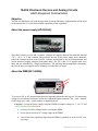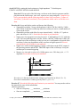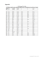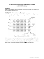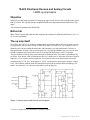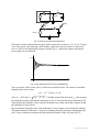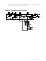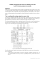
1
Laboratory Assignments These have been used as laboratory assignments along with the books Semiconductor Devices and Technology and Circuit Analysis and Applications. These labs have been carefully coordinated with the material in the texts. This material is copyright D.W. Greve. You can use this material in an academic environment provided the copyright notice is preserved. Reproduction or sale for profit is not permitted. -D.W. Greve Disclaimer This material is provided without warranty or other representation of its suitability for any purpose. The mention of specific part numbers and/ or manufacturers does not represent an endorsement either by the author or Carnegie Mellon University. Even today it is possible to be injured in a laboratory and proper training and safe practices should be followed. Copyright D.W. Greve, 2012 1 18-220 Electronic Devices and Analog Circuits Lab#1-Equipment Familiarization Objective This lab will familiarize you with the operation of various laboratory equipment that will be used in subsequent labs. You will also learn the capabilities of the equipment. About the power supply [HP E3630A]: Note there is both a ground and a common. Voltages are supplied between the terminals marked -20 V, +20 V, +6 V and common. The ground is the case of the power supply and is normally tied to the common for best noise rejection. Voltages are adjusted by the two potentiometers and can be measured roughly using the front panel meter. The -20 V and +20 V supplies track each other and are controlled by a single potentiometer. The tracking ratio potentiometer determines the ratio of these two supplies and is normally set so that they are equal. About the DMM [HP 34405A]: To set up for DC or AC measurements press the appropriate button in the top row. For measuring voltage or two-terminal resistance use the two right-hand upper terminals. The and buttons set the range and < and > set the number of digits displayed. Exercise 1. Set up the power supply using the DMM for output voltages of +/- 18.5 V and +4.5 V. Record in your notebook accuracy to which voltages can be set using the DMM lowest (most sensitive) DC voltage range on the DMM value of the least significant digit when the DMM is operated on its lowest DC voltage range. Copyright D.W. Greve, 2012 1 Resistance measurements are sometimes performed to check continuity or to verify the values of components. Exercise 2. Attach two leads with alligator clips to the two upper right hand terminals and set the DMM to measure two-terminal resistance. Measure the resistance of five 1 k and five 100 k resistors from the parts bin. Record these resistances (to at least three significant figures) in your notebook. Determine the average resistance and the maximum deviation from the average resistance. Are these resistors within a 5% tolerance of the nominal value? Record your conclusions in your notebook. About the oscilloscope [Agilent DSO 7012B]: The user manual for the oscilloscope is located at http://cp.literature.agilent.com/litweb/pdf/54695-97025.pdf. See pg. 35 for an explanation of the front panel controls. Note that the AUTOSCALE button is often a good way to quickly set up a measurement. Not all measurements can be set up using the AUTOSCALE button, however, and it is necessary that you become familiar with other controls on the oscilloscope. Modern oscilloscopes are feature-rich. To learn how to do a particular measurement we recommend one or more of the following: Use the autoscale function and then adjust sweep rate, vertical scale, etc. to obtain the display you need. Refer to the manual. Use the oscilloscope’s built-in help function. Explore the various menus and sub-menus on the oscilloscope. Ask for help from your TA.1 1 While we expect you may need help with a new or unfamilar measurement, we expect you to learn, and remember, how to perform basic functions with the oscilloscope. Copyright D.W. Greve, 2012 2 Exercise #3. Before using the oscilloscope to do measurements you should compensate the probes. The procedure for probe compensation is described on pg. 56 of the user manual. Sketch in your notebook the displayed waveforms for the built-in square wave for both properly compensated and improperly compensated probes. About oscilloscope probes. The figure below shows the 10:1 attenuating oscilloscope probe (left). Attenuating probes are used to minimize the oscilloscope loading on sensitive circuits. The compensation is adjusted using the screw visible on the side of the BNC connector end. The figure on the right shows the other probe parts: a probe head (1); a screwdriver for adjusting the compensation (5) and a clip-on ground connector (6). The head and ground connector can be removed but should always be re-attached before putting the probe away. adjusting screw on side Do not confuse the oscilloscope probe with the BNC to grabbers cable (below). This cable is used to connect the signal generator to circuits and/ or for oscilloscope measurements when loading of the circuit is not expected to be significant. Exercise #4. With the probe properly compensated determine the rise time (defined as the time required to get from 10% of the final value to 90% of the final value) of the built-in square wave. Enter the result in your notebook. Copyright D.W. Greve, 2012 3 Some advice on using the oscilloscope Dear students, there's a matter That I feel I must address. Oscilloscopes have SEVERAL TYPES Of buttons you must press. Why, some of them zoom in or out, Or specify axes; If your waveform is invisible, Try firstly checking these. Your circuity is fine! you say, But nothing's on the scope? Fear not, it's there, just out of sight. Recalibrate, don't mope! You see, you've got to understand That when you auto-scale, The chance that it will zoom correct Approaches 'epic fail'. We TAs love to help you, so, we're teaching you the keys; trust not the power of auto-scale, and lab will be a breeze. -Reuben Mikes, 2008 About the function generator[Agilent 33220A]: There are four standard waveforms accessible using the middle row of buttons. Each of these standard waveforms has several parameters which can be set (at minimum these include frequency and amplitude). The manual (found at http://cp.literature.agilent.com/litweb/pdf/3322090002.pdf) contains a quick-start guide for this instrument. The instrument can be set to display on its front panel the signal amplitudes into either a 50 ohm load OR into an open circuit.2 In this course you will generally use high-impedance loads so you 2 The significance of output impedance will be more clear when we discuss Thevenin and Norton equivalent circuits in class. Copyright D.W. Greve, 2012 4 should BEGIN by setting the load resistance to “high impedance.” To do this press UTILITY>OUTPUT SETUP>LOAD>HIGH Z. Exercise #5. Set up each of the following waveforms on the function generator and display them on the oscilloscope: sine wave; square wave; ramp; and pulse. Complete a table in your notebook with the following entries for these four waveforms: (1) name of waveform, (2) sketch of waveform (3) list of parameters which can be set for this waveform. Exercise #6. Set up and display on the oscilloscope the following: Sinusoidal waveforms. Set up with frequencies 100 Hz, 500 Hz, 1000 Hz, 5 MHz and 15 MHz. Adjust the oscilloscope time base so that you can see a small number of cycles on the screen. Sinusoidal waveform with offset. Set up a sinusoid with f = 100 Hz, 6.5 V peak-topeak and offset of +1.0 V. Sketch this waveform in your notebook. Square wave. Set up square waves low level of -1 V and high level of +5 V with duty cycle3 80% and with frequencies 100 Hz, 500 Hz, 1000 Hz, 5 MHz and 15 MHz. Set the time base of the oscilloscope so that you can see a small number of periods of the waveform. Is there any degradation of the waveform at high frequencies? Record your qualitative observations in your notebook. Square wave with external triggering. Connect a cable between the SYNC output of the function generator and the EXT TRIGGER input of the oscilloscope. Set up the oscilloscope for external triggering. Measure rise time and overshoot of a 1 MHz square wave, 50% duty cycle, +/- 5 V amplitude. Record the results in your notebook. tr v (t ) VH 90% t VL 10% 0% Rise time (tr) is the time it takes for the voltage to go from 10% to 90% of |VH - VL|. Overshoot is measured in % and is given by 100% /(VH - VL). Exercise #7. Record the following specifications in your notebook. You may need to refer to the manuals for some of this information. (function generator) Sine wave frequency: ___ maximum ____minimum Sine wave amplitude: ___ maximum ____ minimum 3 A duty cycle of 80% means that 80% of the period is at the high value and 20% is at the low value. Copyright D.W. Greve, 2012 5 DC offset of sine wave: ___ maximum ____ minimum output impedance: ____ (oscilloscope) Sweep time/ division: ___ maximum ____ minimum Sample rate: ____ maximum Bandwidth: ____ input impedance: ____ Computer/ oscilloscope Log in using to your user account. (Click through the Windows annoyances so you won’t have to do it next time). Use the oscilloscope interface application 220Scope2011.exe to acquire a snapshot of a 1 MHz square wave. Email the image to your email account. (You do not need to submit it but you will need to do this in later labs). To run 220Scope2011.exe: Launch the application from the programs list. You will need to choose the oscilloscope from the list of instruments if other instruments are connected. If no instruments appear in the list then check with your TA. Locate the Ledit program. This program will be used in the next lab. To run Ledit, double click the Ledit icon to run the program. Ledit should run in the correct 256 color compatibility mode. If it does not, consult your TA. 1. Click File > open, select ledit start.tdb from the directory. 2. Explore the menu and get familiar with the graphic user interface. Turn off the equipment, clean up the work bench and log off Windows. Lab Test You must successfully complete the lab test in order to get full credit for the lab. Your TA will give you a description (text or equation) of a common waveform. You must set up this waveform on the function generator and display it on the oscilloscope in 2 minutes. Examples of possible waveforms are: a sine wave with offset with a particular frequency; a symmetric square wave with a given frequency and amplitude, a triangle wave with particular frequency and amplitude, etc. Copyright D.W. Greve, 2012 6 18-220 Electronic Devices and Analog Circuits Lab#2-Hall and pn junction devices Objective This lab will measure the carrier mobility and carrier concentration of a Hall element. In addition the current-voltage characteristic of a pn junction (light emitting diode) will be measured. Circuit board You will perform experiments using a circuit board that illustrates many of the devices and analysis techniques developed in lecture. The circuit diagram is shown below. The circuit board is powered by a 1.5 V battery. The Hall element H1 produces a differential voltage between probes PRB and PRA that is proportional to the magnetic field. The voltage drop across the resistor R1 allows measurement of the current flowing through the Hall element. The differential voltage is connected to an op amp comparator and optionally to an inverting op amp stage (U1). These stages produce an output that swings between approximately ground and approximately 1.5 V. When the output is high it enables a DC to DC converter (PC1) which produces a nominal output voltage of 3.3 V. This high voltage is applied to a switched resistor string R5-R9 in series with a green LED D1 and a current-sensing resistor R10. Test circuit for this lab. The top switch is labeled SW6 on the circuit board and the bottom one SW1. When a switch is in the ON position it is closed. The following figure shows the design of the printed circuit board. Note that components and probes are labeled in this figure but not on the printed circuit board. Copyright D.W. Greve, 2012 Circuit board layout for this lab. Electromagnet design and construction You have available enameled copper wire, AWG 24. The table in the appendix lists the properties of this type of wire. Design an air-core electromagnet coil that will produce a magnetic flux density at the Hall element of approximately 10 gauss. You will have available coil forms with diameters of 6 cm and 4.8 cm. (You can also bring your own form if you wish. The top of a spray can works particularly well). FINISH YOUR DESIGN BEFORE LAB, TA will check your design before you start!! The magnetic flux density produced by a loop of n turns, of radius a, and a distance z from the loop plane is given by n 0 I coil a 2 . B 2( a 2 z 2 )3 / 2 where 0 = 1.26 x 10⁻⁶ H/m.1 Use z = 1 cm for your design.Your completed coil should look similar to the photograph below. You should choose the radius and number of turns. Record your design dimensions and your calculations in your lab notebook before arriving at lab. Also calculate the total length of the wire so you can cut the correct amount from the spool. 1 You can use the conversion 1 H/m = 106 gauss-cm/A. Copyright D.W. Greve, 2012 Photograph of a coil. As general guidance: a large number of turns produces a larger field which will enable more accurate measurements. However winding many turns is tedious and it becomes difficult to keep the coil together when done. Also keep in mind that there is a maximum voltage and current available from your power supply. Finally, high power dissipation in the coil causes it to heat up and in extreme cases the copper wire can melt. When you are done winding the coil remove the enamel from the wire ends using sandpaper. Measure the resistance using your DMM and record it. Be sure to keep the coil after this lab as we will use it again in a later lab. Hall measurement The figure below (adapted from the text) defines dimensions and voltages relevant to this experiment. V z y x VH Bz I t w l Locate your coil with its center directly underneath the Hall element. Measure the distance between the Hall element and the coil plane. Insert the 1.5 V battery (OBSERVE POLARITY!) and attach the coil to your power supply. If the LED lights up move SW6 to the opposite position to turn the LED off. If neither position turns off the LED you should set SW1- SW5 to the open position and then proceed with the laboratory. In the following, limit the coil current to about 1 amp. Record the actual coil current Icoil in your notebook. Copyright D.W. Greve, 2012 With zero coil current measure the voltage drop across resistor R1 and the actual battery voltage. Use a table like the one below to record your data and analyze it to determine V and I for the Hall element. VR1 (volts) Vbattery (volts) V (voltage across Hall element) = Vbattery-VR1 I (current through Hall element) = VR1/(100 ) Now connect the DMM to the sensing terminals PRA and PRB. Using the most sensitive range available measure the DC voltage between the two sensing terminals (This will not be exactly zero because the Hall element is never precisely symmetric). Record the voltage between the sensing terminals PRA and PRB (a) with zero coil current and (b) with current flowing clockwise (viewed from above) through the coil. Repeat the measurements and enter the measurements in your notebook in a table like the one below. Check the battery voltage to see if it has changed significantly (If it has, repeat the measurements with a fresh battery. A “significant” change is a decrease of more than 5%). Finally, compute VH as the average of the differences between zero coil current and coil current on. VPRAVPRB (coil current off) VPRAVPRB (coil current on) VH measurement #1 measurement #2 measurement #3 measurement #4 average Make a careful sketch of the apparatus in your notebook. Analyze your data to determine the carrier mobility and carrier concentration.2 (This analysis can be done after lab). Assume that the Hall element is 0.2 10-4 cm thick and w/l = 2 (definitions as in the lecture notes). We suggest you proceed in the following order: 1. Determine the carrier concentration. Use the equation I VH Bz qct where c is the total carrier concentration (can be either the electron concentration or the hole concentration.) 2. Find the conductivity of the material making up the Hall element. For the resistance we have V 1 l R I wt 2 1 gauss = 10-8 Vsec/cm2. Copyright D.W. Greve, 2012 3. Determine the carrier mobility. You can assume that the charge carriers are predominantly either electrons OR holes. We have qc c where c is the concentration of the predominant carrier and c is the carrier mobility. Since you know c from step 1, you can calculate the mobility c. Record these steps and the final results for carrier concentration and mobility in your notebook. Diode I(V) measurement Begin by identifying the actuators corresponding to switches SW1- SW6. Note that switches are closed when in the ON position. Set all actuators to the closed position. Begin by setting switch SW6 to the position that turns on the LED.3 Using your DMM measure the voltage between probe PR8 and ground and PR7 and ground. Record these voltages along with the switch positions. Now open one of the switches SW1-SW5. Note that the brightness of the LED changes. Opening a switch puts a resistor in series with the LED reducing the current. So if we measure the voltage at PR7 and PR8 we can measure the new value of the diode current (from the voltage across R10) and the new value of the diode voltage (difference between the voltage at PR7 and PR8). Record these values also along with the number of the switch opened. Repeat for all the other switches. Analyze this data to determine the I(V) characteristic of the LED. This analysis can be completed after lab. Plot the data to show the measured I(V) characteristic of the diode on two graphs: (1) linear current as a function of linear voltage and (2) current on a log scale as a function of linear voltage. In your notebook, comment on whether the measurements agree with the diode characteristic derived in lecture. Hints: (1) minimize the time the LED is at full brightness to keep the battery from getting run down. (2) record and analyze the data using a table similar to the one shown below. 3 If both positions turn on the LED then you can use either. If neither position turns on the LED this means that the imbalance in your Hall sensor is too large and you should ask your TA for a bias magnet. This behavior was not anticipated and is a result of non-ideal behavior of the op amps. There is an important lesson here. Copyright D.W. Greve, 2012 switch opened series R V(PR7) V(PR8) I=V(PR7)/22 Vdiode=V(PR8)-V(PR7) SW1 SW2 SW3 SW4 SW5 Before leaving, clean up the lab bench, put away probes, cables, etc. HAVE YOUR LAB NOTEBOOK SIGNED AND DATED BY THE TA BEFORE LEAVING. Lab notebook Include in your lab notebook (1) your design for the electromagnet; (2) a complete description of the experimental setup for the Hall effect measurement together with the collected data; (3) calculations of the carrier concentration and carrier mobility; (4) data from the diode I(V) measurement; and (4) the requested plots of the diode I(V) characteristic. Submit the notebook at the beginning of the next lab section for grading. Extra credit If you are careful with your notes you will be able to determine whether the carriers in the Hall element are electrons or holes. If you can, clearly explain your reasoning and your conclusion. Copyright D.W. Greve, 2012 Appendix Copyright D.W. Greve, 2012 18-220 Electronic Devices and Analog Circuits Lab#3-Transistor layout Objective This lab will (1) provide an introduction to the use of L-edit and (2) to illustrate the design and layout of n-channel and p-channel transistors. SOI-CMOS process In class we have outlined an eight-mask process for fabrication of silicon-on-insulator MOSFETs. Figure 1 shows a CMOS inverter fabricated in this process. (One additional mask level, not shown in class, has been added to provide an opening for wire bonding to the second-level metal.) Figure 1. SOI-CMOS process and mask levels. L-edit student version is a program for the layout of integrated circuits. We will use this program to gain experience with layout and to learn about the different structures that can be fabricated with these nine mask levels. L-edit has one particularly useful feature- a cross-section function that draws a cross section of the result of a mask design. We will use this feature extensively as a learning tool. Design rules A circuit must obey the design rules in order to guarantee successful fabrication. There are several types of design rules. Features drawn in the layers have minimum sizes which are determined by the capability of the fabrication process. Different polygons drawn in the same layer also have a minimum separation which is required in order to guarantee that the objects remain separate during fabrication. Other rules are more complex, and concern the required overlaps between certain layers or the extension of one layer outside another. A list of the design rules is presented in the appendix to this lab. The design rules in this process are intended to be simple to use; they are all expressed as small integer multiples of a parameter Copyright D.W. Greve, 2012 lambda. For example, all contacts must be squares exactly two lambda in size. (A process might have a lambda of a fraction of a micrometer). The grid has been set up with a spacing of exactly lambda between each grid point. Roughly speaking, the value of lambda depends on the sophistication of the process, with more advanced processes having smaller values of lambda. It is necessary to know some or all of the design rules in order to design efficiently. However, it is not practical to rely on a designer to check manually to see that all the rules are satisified. (Keep in mind that advanced circuits might contain many millions of transistors!). Consequently layout applications include a design rule check function which performs this check automatically. Using L-edit Start L-edit by clicking on the L-edit icon on the desktop. Select File> open... and navigate to the file ledit start.tdb in the directory indicated by your TA. You will see a screen similar to Figure 2. Figure 2. Startup screen for L-edit (after opening the file ledit start.tdb). This screen is a color-coded top view of all of the mask levels. The color-coding is as shown in Figure 1 with two important comments: - the Via mask level is white and is therefore only visible when on top of another colored level. - there are two distinct contact levels, one for contact to sources and drains (called the active contact level) and the other for contacts to polysilicon (poly contact). Both are shown as black but they are not interchangeable. Copyright D.W. Greve, 2012 Views and navigating With no other keys pressed, the arrow keys navigate around the drawing. Other useful commands for viewing are View>Zoom>in and View>Zoom>out. If you become lost then Edit>select all followed by View>Zoom>to selections will help. Drawing polygons To draw polygons, begin by selecting the mask level you wish to draw. This is done using the drop-down menu at the left (Figure 3). Then select the rectangle button (or other button for different shapes) and then draw a rectangle with the mouse. Note that there are more than nine levels in the drop-down list. Most of these are derived layers, that is, they are composites of the drawn mask levels. They cannot be drawn directly but are used during the design rule check. The mask levels needed for this lab are in a single vertical row beginning with a red layer (Poly). Figure 3. Detail showing menu for selection of mask level to be drawn and button to select the draw rectangle option. Note the arrow just to the left of the draw rectangle button for selecting polygons. Moving polygons To move a polygon click the arrow button in Figure 3. Then click on the polygon you want to move, press the ALT key, and use the mouse to move the layer. You can also click on an object, press CTRL, and use the arrow keys to nudge the object. You can also stretch an edge by clicking on the edge, pressing the ALT key, and using the mouse. Design rule check To perform the design rule check make the menu selection Tools>DRC... as shown in Figure 4. The existence of errors is indicated by a large X and by some fairly subtle black lines at the location of the error. If there are many errors and/ or if you don’t know what they mean then you can use the mouse to select only the black lines indicating errors in one region. Then zoom out to read the error explanation. Copyright D.W. Greve, 2012 Figure 4. Initiating the DRC check. Figure 5 shows one error indicated. The two red arrows show the black lines L-edit uses to mark the location of an error. If the error location is selected the explanation is shown as in Figure 6. The error was an insufficient extension of polysilicon outside of the transistor active area. Figure 5. Result of a DRC check (one error present). Arrows show the solid lines indicating the error location. Copyright D.W. Greve, 2012 Figure 6. After selecting the error location the description of the error appears. Cross section function To activate the cross section function use the menu selections Tools>Cross section... You will get the pop-up window shown in Figure 7. You may need to browse for the soifet.xst file which contains the process information needed to draw the cross section. Clicking the button Pick... allows you to choose the line along which the cross section is drawn. Finally, it is recommended that you check Auto-fit in window for easiest viewing of the result. Figure 7. Pop-up window for selection of options for cross section command. Figure 8 shows the result of the cross section command. Copyright D.W. Greve, 2012 Figure 8. A cross section drawn by L-edit along the line selected. Files needed: (Download these files as L-edit files.zip from Blackboard. We recommend deleting files already on the lab computer as they may have been modified). ledit start.tdb soifet.tdb T1.tdb-T7.tdb circuit.tdb soifet.xst Lab Assignment Parts 2-4 should be completed in your notebook. Submit a file for part 5. A copy of the .tdb file for this part must be submitted by email to the lead lab TA for your section with filename <first student last name> <space> <second student last name>.tdb. Also make a printout of the layout and attach it in your laboratory notebook. Open the file ledit start.tdb. This file contains one n-channel MOSFET. 1. Explore the L-edit interface. Move and draw polygons; zoom in and out; save files with a different name. Learn the location of the Cross section and DRC commands and use them. Satisfy yourself that the original transistor satisfies the design rules. 2. Open the files T1.tdb-T7.tdb. Examine the transistors and complete a table in your notebook with the following 6 columns: Copyright D.W. Greve, 2012 file name, NMOS/ PMOS/ not transistor, passes DRC?, design error description, Z (if valid transistor), L (if valid transistor). 3. Determine the minimum size transistor for NMOS and PMOS transistors. For each transistor type determine: the minimum Z, minimum L, and area of n select or p select mask for the minimum size transistor. Enter this information in your notebook along with a sketch or image of the minimum size transistor. 4. Open the file circuit.tdb. Note that gnd and VDD are labeled and two terminals are labeled A and X). Draw the circuit and label all terminals on the circuit. Also label all transistors with the Z/L ratio. 5. Design a CMOS inverter with minimum channel length for both transistors, 20 m NMOS width, and 60 m PMOS width. Assume that lambda for the process is 0.5 m. Submit the design with labeled input, output, ground, and VDD. Include on the design the total area (n select area + p select area). Appendix The following figure and table illustrate some of the essential design rules for laying out transistors. You may encounter additional design rules if you make a design very different from example transistors. The design rule description will help with troubleshooting in these cases. Design Rules: 2.1 Active Minimum Width 3.1 Poly Minimum Width 3.2 Poly to Poly Spacing 3.3 Gate Extension out of Active 3.5 Poly to Active Spacing 4.2a/2.5 Active to N-Select Edge 4.2b/2.5 Active to P-Select Edge 5.1A Poly Contact Exact Size Type: Minimum Width, Distance: 3.000 Lambda Type: Minimum Width, Distance: 2.000 Lambda Type: Spacing, Distance: 2.000 Lambda Type: Extension, Distance: 2.000 Lambda Type: Spacing:I:E, Distance: 1.000 Lambda Type: Surround:I:O, Distance: 2.000 Lambda Type: Surround:I:O, Distance: 2.000 Lambda Type: Exact Width, Distance: 2.000 Lambda Copyright D.W. Greve, 2012 6.1A Active Contact Exact Size 6.2A Active Overlap of ActiveContact 6.4A Active Contact to Gate Spacing 7.1 Metal1 Minimum Width 7.2 Metal1 to Metal1 Spacing 7.3 Metal1 Overlap of PolyContact 7.4 Metal1 Overlap of ActiveContact Type: Exact Width, Distance: 2.000 Lambda Type: Surround:I:O, Distance: 1.000 Lambda Type: Spacing, Distance: 2.000 Lambda Type: Minimum Width, Distance: 3.000 Lambda Type: Spacing, Distance: 3.000 Lambda Type: Surround, Distance: 1.000 Lambda Type: Surround, Distance: 1.000 Lambda Copyright D.W. Greve, 2012 18-220 Electronic Devices and Analog Circuits Lab#4-SRAM design Objective In this lab you will design unit cells of an SRAM. You will gain experience with minimizing the area occupied by a particular circuit. SRAM (Static Random- Access Memory) An SRAM is a regular array of cells, each of which stores one bit of information. Figure 1 shows how the array is organized. In this diagram wires running vertically are known as bit lines and wires running horizontally are word lines. Figure 1. Schematic layout of an SRAM. Each cell consists of two cross-coupled inverters and two access transistors (Figure 2). Note that there are also horizontal lines for the positive power supply and ground. In operation one particular row of cells is accessed by raising the corresponding word line high while all other word lines are held low. To read information the voltages appearing on BL and B L lines are detected by the output circuitry. Information is written by forcing BL and B L to particular values. Copyright D.W. Greve, 2012 VDD WLi GND BLi B Li BLi 1 B Li 1 Figure 2. Detailed circuit diagram of two SRAM storage cells. SRAM cell design In this lab you are to design cells which will be repeated in order to form the memory array. Your objective is to design a functional circuit while minimizing the area occupied by each cell. Review the design rules for metallization and vias (appendix to this lab). Then lay out one cell with BL and B L running vertically using Metal2 and WL , GND, and VDD running horizontally in Metal1. When you have a single cell designed, copy it and assemble into an array (say, a 4 4 array). When you have completed the design you must demonstrate to the lab TA that your design satisfies the design rules. If your design passes the design rule check you can proceed to collect information for the lab report. Design optimization (optional) Your first design is undoubtedly not optimized. If you wish can attempt to improve the design. For this class we will focus only on the area occupied by the cell which should be minimized. In order to optimize your cell things to consider include: choice of interconnect level to be used for VDD, WL, BL and B L (choices are Metal1, Metal2, poly, and source/ drain regions); merging transistors with common source or drain contacts; sharing contacts between cells; transistor orientation; non- rectangular cells; etc. etc. Lab report contents In your lab notebook include: introduction/ objective; snapshot of design;1 description of design including Z/L of transistors and interconnect levels used; the area of the repeated cell in units of lambda; and the total area in cm2 of cells in a 1 Mb (= 1,048,576 cells) memory if lambda = 0.25 m. A copy of the .tdb file must be submitted by email to the lead lab TA for your section with filename <first student last name> <space> <second student last name>.tdb. 1 To obtain an image of a particular active window: Alt-Prnt Scrn. Paste into a document and save while still in 256color mode. Copyright D.W. Greve, 2012 Appendix The figures below summarize the different types of interconnections between layers and the more important design rules for the metallization layers. Various connections between layers. Left to right: Metal1 to Metal2 Metal1 to Metal2 on top of poly, no contact to poly Metal1-Metal2-poly connection Metal1 to poly, Metal2 on top but not connected; and Metal1 to poly. Direct contact between Metal2 and poly is not permitted. Copyright D.W. Greve, 2012 Summary of important design rules. Design Rules: 3.1 Poly Minimum Width 3.2 Poly to Poly Spacing 5.1A Poly Contact Exact Size 7.1 Metal1 Minimum Width 7.2 Metal1 to Metal1 Spacing 7.3 Metal1 Overlap of PolyContact 7.4 Metal1 Overlap of ActiveContact 8.1 Via Exact Size 8.3 Metal1 Overlap of Via 9.1 Metal2 Minimum Width 9.2 Metal2 to Metal2 Spacing 9.3 Metal2 Overlap of Via1 Type: Minimum Width, Distance: 2.000 Lambda Type: Spacing, Distance: 2.000 Lambda Type: Exact Width, Distance: 2.000 Lambda Type: Minimum Width, Distance: 3.000 Lambda Type: Spacing, Distance: 3.000 Lambda Type: Surround, Distance: 1.000 Lambda Type: Surround, Distance: 1.000 Lambda Type: Exact Width, Distance: 2.000 Lambda Type: Surround, Distance: 1.000 Lambda Type: Minimum Width, Distance: 3.000 Lambda Type: Spacing, Distance: 4.000 Lambda Type: Surround, Distance: 1.000 Lambda Copyright D.W. Greve, 2012 18-220 Electronic Devices and Analog Circuits Lab#5-op amp basics Objective In this lab we gain some experience wiring up op amp circuits and we will verify the basic operation of circuits. We will also become acquainted with some important non-ideal behavior of op amps. You will need a protoboard to do this lab. Before lab Make Table I in your lab notebook and complete the columns for G(ideal) and G(exact). Use A = 105 in your calculation. The op amp itself We will use the LM741, an old design with moderate performance that is still used in many noncritical applications. An enormous variety of different op amps is available (see, for example, ti.com or national.com) with specialized characteristics and sometimes very high performance. However a high-performance op amp is like an exotic sports car- very high performance, but very easy to wrap around a telephone pole. In this lab we will be working with the Toyota Corolla1 of op amps. The specifications of this op amp can be obtained from national.com. The pinout is presented in figure below. Also shown is the circuit diagram (We won’t need to use it. Note that it has lots of bipolar transistors, a few resistors, and one capacitor. If you want to know more about analog electronics, consider taking 18-320, etc.). In the pinout V+ and V are the positive and negative supplies, respectively. The terminals marked offset null should not be used (do not connect them to anything). (NC means “no connection” so it doesn’t matter what you do to that pin.) Figure 1. Op amp pinout and internal circuit diagram. 1 As usual, no endorsement of a manufacturer or product is implied. Copyright D.W. Greve, 2012 The inverting configuration Build the circuit of Fig. 2 on your protoboard. Note that the power supplies are not shown- you must connect the + and power supplies to the appropriate pins. Use power supplies of +15 V and 15 V. Don’t forget to wire the power supply common to the protoboard as it needs to be connected to the ground in the circuit. (It may be beneficial to connect the G terminal on the power supply to common also. However this will probably not be necessary). Use R1 = 1 k and R2 = 1 k. R2 R1 vI vO Figure 2. Inverting configuration. Begin with the signal generator set to supply a 20 V peak-to-peak sinusoid at 100 Hz. Use the oscilloscope to measure the peak-to-peak amplitudes of the input and output signals as accurately as you can. Make a table like the one below in your notebook and enter the measured closed-loop voltage gain. R2 vI (p-p) 1 k 20 V 10 k 2V 100 k 0.2 V 1 M 0.02 V G(ideal) G(exact) G(measured) Table I (sample). Now change the value of R2 to 10 k, decrease the amplitude of the sine wave to 2 V peak-to-peak, and repeat the measurement. Continue with R2 = 100 k and 1 M. Enter in the table the ideal closed-loop voltage gain (calculated using the virtual short method) and the exact voltage gain (calculated using the specified voltage gain A = 105). Comment on whether you have obtained good agreement with measured and calculated gains. Finally, estimate the output resistance of this circuit. Using R2 = 100 k and an input voltage of 0.2 V peak-to-peak, connect resistors of 10 k, 1 k, and 100 at the output. Do you see any change in the output voltage as the load resistance is varied? Use your result to either calculate a value for the output resistance OR place an upper limit on its value. HINT: The output voltage is vO ( RL /( RL RO ))vO ,OC , where RO is the output resistance, RL is the load resistance, and vO,OC is the output voltage with RL = . Copyright D.W. Greve, 2012 Summing amplifier Here we will build a circuit to obtain a sinusoidal voltage with a DC offset. Figure 3 shows a summing amplifier. Use R2 = 10 k and design a circuit (that is, choose values for Ra and Rb) that will produce a 3 V peak-to-peak sinusoid with a DC offset of 2 V. Use the 0 to 6 V supply of your power supply for vI2 and use the function generator for vI1. Verify operation using your oscilloscope. Include in your notebook (1) a complete circuit diagram with all components labeled and (2) sketches or screen captures showing the output waveform. Ra vI1 R2 Rb vI 2 vO Fig. 3. A summing amplifier. Offset voltage- nonideality #1 Ideally the output voltage will be zero if v+v is zero. Try this- connect the two inputs to ground and measure the output voltage (Fig. 4). Record the result in your notebook. vO Fig. 4. Op amp with zero differential voltage input. Unless you are very very lucky, you will see an output voltage either close to +15 V or 15 V (that is, the op amp will be saturated at one or the other of the two power supply voltages). This happens because there is always a small imbalance between the two inputs. This imbalance varies from one unit to another and may be either positive or negative. This imbalance can be modeled by a voltage source in series with one of the inputs of value VOS (Fig. 5). In this figure the dotted line is the “real” op amp which is modeled by an ideal op amp and an attached voltage source VOS. R2 R1 VOS vO Fig. 5. Real op amp with an additional voltage source to model the offset voltage. Copyright D.W. Greve, 2012 To measure the offset voltage, set up the circuit of Fig. 5 with R1 = 1 k and R2 = 1 M. The output voltage is given by R vO 1 2 VOS R1 Measure the offset voltage for five op amps. Put the result in a table and calculate the average offset voltage magnitude |VOS|. This average offset voltage magnitude (which is incidentally a parameter on the op amp data sheet) is one source of DC error in op amp circuits. Output voltage limitations- nonideality #2 The ideal op amp transfer characteristic (Fig. 6) saturates at VDD. In real op amps the output voltage may not reach these ideal limits. VDD vO v O A ( v v ) v v VDD Figure 6. Ideal op amp transfer characteristic. Set up the circuit of Fig. 2 with R1 = 1 k and R2 = 10 k. Using a sinusoidal input at 100 Hz, gradually increase the input voltage until saturation begins to occur. This may not occur at precisely the same voltage for positive and negative limits. Record your observations in your notebook. Also accurately sketch or (better) attach a screen capture showing (1) output waveform just before saturation; (2) showing the beginning of saturation on one polarity and (3) showing saturation for both polarities. Now set the input voltage to give an output swing from -10 V to +10 V. Increase the frequency and observe what happens. Make accurate sketches or (better) attach screen captures showing your results. (Increase the frequency to at least 100 kHz.) Copyright D.W. Greve, 2012 18-220 Electronic Devices and Analog Circuits Lab#6-op amp applications Objective In this lab we explore some op amp applications. These applications use more than one op amp and possibly some other devices in order to perform a useful function. You will need a protoboard to do this lab. These are multi-op amp circuits and as a result there are many opportunities for errors. The appendix contains recommendations for wiring and troubleshooting. Before lab Calculate the resistor values required for the peak detector portion of the lab (below). Draw a circuit in your lab notebook labeled with the resistor values you have chosen. Your TA will check your design at the beginning of lab. Peak detector Figure 1 shows the circuit diagram of a peak detector. The purpose of this circuit is to indicate when the input signal exceeds a particular maximum value in either the positive or negative direction. Such a circuit might be used when doing audio recording, to determine when the input signal is large enough to saturate the electronics. The first two op amps are used as comparators, where the comparison voltage is derived from a voltage divider. Note that the output of the upper comparator becomes +15 V when the input signal exceeds the voltage at the junction of R1 and R2. The lower comparator output becomes +15 V when the input is less than the voltage at the R2-R3 junction. We can call these two switching voltages the upper and lower thresholds Vth+ and Vth-. Copyright D.W. Greve, 2012 15 V 15 V 15 V R6 R1 R4 R7 Vth vI 1 R2 Vth Vb R5 Va R3 15 V Figure 1. Peak detector circuit. Before lab you need to choose the resistor values required for this circuit. Design to satisfy the following requirements: 1. The upper and lower threshold voltages Vth+ and Vth- are +1.5 V and -1.5 V, respectively. 2. The voltage Va is greater than 0 V if vI1 > Vth+ OR vI1 < Vth-. If vI1 is between these two values then Va < 0. (The Thevenin theorem may help here). 3. The current through the LED is 5 mA when Vb = +15 V. Note that resistors are available only in discrete values.1 As a result you will not be able to set precise values; you should aim to get within 10% or so. Build the circuit with the values you have chosen. Begin testing your circuit by applying a variable DC voltage at the input (obtained, for example, using the DC offset on your function generator). Using your oscilloscope verify that the circuit works as expected. We suggest that you work your way from input to output, checking voltages along the way. In your notebook, draw the complete circuit including all component values. Include a table with the measured voltages at nodes Va and Vb for vI1 = +5 V, vI1 = 0 V, and vI1 = 5 V. (Note: we mean measured values not the theoretical values that you expect!). (There are two ways to generate 5 V. The first way is to use voltage division with resistors between -15V and ground, the second way is to use the function generator by setting the amplitude to a very small value and offsetting the output by 5 V). Analog to digital converter In a great many applications analog signals are converted to digital signals for storage, signal processing, display, etc. etc. For example, in a recording studio the signals from microphones are amplified, converting it to digital form, and stored on a hard disc. Mixing takes place in the digital domain and the final recording is recorded on a CD as a sequence of digital samples. The conversion of the analog signal to digital form is performed by an analog to digital converter (A/D for short). This is illustrated in Figure 2. At a particular time ts we assign a digital code depending on the analog signal amplitude (sometimes this is called quantization). Of course we can only approximate an analog level in this way because there are only a finite number of digital codes available. High-quality signal acquisition may use digital 12 or 16 bits (corresponding to 1 See http://www.elexp.com/t_eia.htm, or do a search on the web for “standard resistor values.” Copyright D.W. Greve, 2012 212 = 4096 or 216 = 65536 distinct levels). In this section we examine the operation of a two-bit analog to digital converter. v (t ) 001 111 110 101 100 011 010 001 ts 2t s 4t s 3t s t Figure 2. Analog to digital conversion of a signal. The particular design we will examine is shown in Figure 3. This is a flash A/D, so called because its speed of acquisition is limited only by the response time of a comparator.2 Note that in this case we are using the op amp with a single +10 V power supply. 10 V 10 k v04 10 k vO 3 10 k vI1 vO 2 10 k 10 V v 01 10 k Figure 3. A flash A/D converter. Wire up the circuit as indicated. The grayed portion of the circuit is optional and uses four LEDs that can be to visualize the operation of the circuit. If you do this (optional) portion of the lab, set up the function generator to produce a 0 V to 10 V ramp with a frequency of 1 Hz. Use 1 k resistors in series with the LEDs. Attach this signal as the input, sit back, and watch the lights. Now set up your function generator to produce a 0 V to 10 V ramp with a frequency of 1 kHz and use your oscilloscope to monitor the input signal and one of the outputs. Use the NORM trigger mode with an external trigger derived from the function generator to obtain a stable display.3 Examine and acquire a snapshot of each of the outputs in turn. Paste each of these plots in your notebook and carefully label them. 2 Flash A/D converters are practical only for small numbers of bits. Sometimes they are used as part of a higherresolution A/D. There are several different designs of A/D converter that differ in complexity, speed of response, and resolution. Your DVM is at the other extreme; it has a fairly slow A/D with very high resolution. 3 If you use AUTO instead of NORM the various outputs will not have the same time reference. Copyright D.W. Greve, 2012 Note that there are 22 = 4 distinct levels and 4 digital outputs. Include in your notebook the truth table of a combinatorial digital circuit that converts these four outputs into a two-bit digital word. In your truth table, assume that an input voltage less than 2 V should output a digital code of 00. Ramp generator (oscillator) Figure 4 shows an oscillator circuit using two op amps. In this circuit use +15 V and 15 V supplies. This circuit uses two circuit configurations we have not discussed in class. i C 0. 1 F 22 k 10 k 10 k vO 2 vO 1 Figure 4. Ramp generator circuit. We will first explain briefly the operation of two op amps in Fig. 4. The first op amp circuit is an integrator. Let’s calculate the output voltage vO2 as a function of vO1. By the virtual short method, iC = vO1/R = C(dvC/dt) = C(dvO2/dt). Solving for vO2 we get t vO 2 (t ) vO 2 (0) 1 vO1 (t )dt RC 0 where R and C are the resistor and capacitor values, (here 10 k and 0.1 F, respectively). The second op amp is a Schmitt trigger. Note that the feedback is to the + input; this is not an inverting amplifier! The transfer characteristic vO2(vO1) of the Schmitt trigger has hysteresis; that is, the output voltage depends on the previous history. A brief explanation is as follows: Suppose vO1 is +15 V and vO2 = 0 V. By voltage division, the voltage at the + input of the Schmitt trigger is positive so this is consistent with an output voltage of +15 V. Since vO1 is +15 the integrator output vO2 starts to ramp to negative values. As vO2 decreases the + input of the Schmitt trigger becomes more negative. Eventually the voltage at this input will become less than 0 V. When this happens the output vO2 will switch to -15 V because the sign of v+ v will reverse. Now the input to the integrator stage is negative, so the voltage vO1 will ramp up. Eventually the Schmitt trigger will switch in the other direction. (The transfer characteristic of the Schmitt trigger is shown in Fig. 5.) So we expect to see a linear ramp generated at vO2 and vO1 will switch between the two limits +15 V and 15 V. Copyright D.W. Greve, 2012 vO 2 15 V vO1 15 V Figure 5. Transfer characteristic of Schmitt trigger in Fig. 4. Build the circuit of Figure 4 and verify its operation by using the oscilloscope to examine the waveforms at vO1 and vO2. Measure the frequency of the waveforms. Now redesign the circuit to produce outputs at a frequency of 400 Hz. Record the waveforms and attach them to your notebook along with a complete sketch (with all component values) of your design. Appendix on troubleshooting The ability to systematically and efficiently troubleshoot a complex system is a valuable skill which you will need many times in your career. The approaches suggested here will be helpful not only in circuits and other experimental courses; similar approaches will be useful in programming or computer modeling. 1. Make it less likely that you will have problems. Work neatly and systematically. Good analog layout requires short, direct leads. Use rails for positive and negative power supplies and ground. Arrange the circuit logically. Make solid connections to power supplies, input sources, and measuring instruments. Try to keep all signal lines away from power lines, and in general keep all lines a short as possible. Long signal paths and power supply lines running near signal paths are susceptible to noise pickup and coupling. Clip component leads and wires, and try to get components flush with the surface of your protoboard. A great many faults are due to poor connections. An old protoboard may have damaged clips . If you have doubts about your protoboard, get a new one and treat it kindly. Make sure you have a solid ground reference. (Think about all the instruments: power supply, signal source, and oscilloscope.) 2. Build a complex system in pieces and test each part. 3. Proceed logically. Make a hypothesis as to why the circuit doesn't work and test the hypothesis. For example: one hypothesis is that there is no power applied to the circuit. Use your oscilloscope to check the protoboard for power. If there is power make another hypothesis. Your second hypothesis could be that the op amps are operating in the saturation region or are damaged. Measure the DC voltages at inputs and outputs of the op amps. If you find a problem make hypotheses about its cause (in- Copyright D.W. Greve, 2012 correct wiring, bad connection, failed chip, etc.) Next, follow signals from input to the output, checking amplitudes along the way, etc. etc. 4. Keep the probabilities in mind. Connectors (to components or other equipment) are highly likely to cause problems. Wiring mistakes are likely especially if you are not neat. Chips sometimes burn out (especially in lab where they may have been incorrectly connected). Resistors burn out very rarely (and usually smoke beforehand) and capacitors also rarely fail. Instruments do fail (although seldom) and in any case you can test them (connect your oscilloscope to the function generator!) 5. Be self-reliant. Your TA is not there to find your wiring mistakes. He (she) will make suggestions and give hints, however. Portion of a carefully- organized protoboard. Copyright D.W. Greve, 2012 18-220 Electronic Devices and Analog Circuits Lab#7-Transients Objective In this week’s lab, we will examine the transient response of RC and RLC circuits. This lab will use the coil from Lab #2. Be sure to bring it to lab. Also bring a protoboard. Oscilloscope and function generator operation (advanced) Advanced oscilloscope triggering You can set the trigger source, the trigger conditions, and the trigger mode. Trigger mode (press MODE/ COUPLING) AUTO trigger mode triggers when the trigger amplitude and slope condition are satisfied; but if no trigger occurs in a particular time the oscilloscope triggers anyway. The time before automatic triggering is a few ms. AUTO mode is good when setting up the oscilloscope because you will see a display and some sort of signal even if the trigger is not set properly. NORM mode means the oscilloscope does not trigger unless the trigger condition is met. No trigger, no trace. HOLDOFF is a wait time before the next trigger occurs. This will be useful later when we want to trigger on a sinusoidal burst, because otherwise there are many different times during a burst when the trigger condition is satisfied. Set the holdoff by pressing the HOLDOFF menu button, then turn softknob ( ) trigger conditions and source To set these push the TRIGGER button. The leftmost soft button should be set to TRIGGER EDGE. Use the other soft buttons on the screen to select: source (Channel 1, Channel 2, or External) and trigger slope (slope at which the signal must cross the trigger level). The trigger level itself is set using the TRIGGER control. s Advanced oscilloscope channel settings We will need to set both channels on. To do this activate both the 1 and 2 buttons. After each is pushed you can select the BW LIMIT button. This decreases the bandwidth of the oscilloscope which has the effect of reducing the displayed noise. Use this button if you are looking at low level signals. Advanced function generator settings We will need to set up a sinusoidal burst signal (several cycles of a sinusoid separated by a gap). To set up a sinusoidal burst FIRST set the sinusoid frequency and amplitude (press SINE, set up frequency and amplitude as usual) THEN set up the burst (press BURST select N CYCLE, (this activates the mode) select # CYCLES, set number of cycles select START PHASE, set start phase in degrees select BURST PERIOD, set length of burst plus gap) D.W. Greve, 2012 Exercise. Set up the following waveform and obtain a stable display on the oscilloscope. 5 cycles of a 1 kHz sinusoid with 5 V amplitude followed by a 20 ms gap. Signal to start at 0 degrees. Show the display to your TA before proceeding with the rest of the lab. RC circuit Set up the RC circuit in Fig. 1 where R = 3.3 k and C = 0.1 F. The source is the function generator and CH1 and CH2 indicate where the oscilloscope probes for the channel 1 and channel 2 are to be attached. CH1 CH2 R vS C Fig. 1. RC circuit. We will first examine the response of the circuit to a step. Set up the function generator to produce a square wave of 5 ms period with low value of 0 V and high value of 5 V. The duration of 5 ms has been chosen so that the capacitor completely discharges or completely charges between transitions. As a result we can assume to an excellent approximation that the capacitor voltage is zero just before the the generator voltages rises from 0 to 5 V. Set up the oscilloscope to obtain stable triggering of the waveform so that the rising edge of the transition is visible on the oscilloscope screen. You should see something rather like Fig. 2. vC (t ) 5V t1 / 2 2 .5 V t Fig. 2. Waveform resulting from step excitation of RC circuit. Measure the time required to reach ½ of the final value of 5 V. Record that value in your notebook and extract the value of the time constant using the equation =t1/2/ln(1/2). Compare this with the calculated value of for this circuit. We now look at the response of the circuit to a more complex waveform. Set up the function generator to produce a waveform consisting of a gated sine wave, that is, 20 periods at f = 10 kHz followed by zero output for the same length of time (Fig. 3). (In this section we want to study the response of the network when a sinusoid is turned on, that is, to the waveform vs(t) = 5sin(t)u(t) volts. We use a gated sinusoid so we can have a repeating signal and also allow enough time for all transients to die away). D.W. Greve, 2012 v S (t ) t Fig. 3. Burst waveform. Use the oscilloscope to observe the exciting signal and the voltage across the capacitor vC(t). Use a slow enough time base to see the entire 20 periods of the sinusoid. You will see something similar to Fig. 4. Note that we can clearly see that the waveform is the sum of the forced response (a sinusoid with a frequency of 10 kHz) and the natural response (an exponential decay). From your captured transient, determine the time constant of the exponential decay. Is this the same as the time constant observed for the step response? Does this make sense? (Report your measured value, and your answers, in your lab notebook). vC (t ) t Fig. 4. RC circuit response to a gated sinusoid. Now let’s consider the amplitude of the sinusoidal component- the forced response. Measure the peak-to-peak amplitude of the sinusoidal component. This will be easiest at larger values of t where the exponential has decayed. Repeat the measurement of peak-to-peak amplitude for frequencies between 1 kHz and 100 kHz. You will need to adjust both the frequency and the burst period to maintain a gap between bursts. Take approximately 10 data points with roughly equal spacing on a log scale (for example, in a 1,2,5 sequence: 1 kHz, 2 kHz, 5 kHz, etc.). Record your data in your notebook in a table. Make a plot of peak-to-peak amplitude on a linear scale as a function of frequency on a log scale. Is this plot consistent with expectations? RLC circuit- underdamped response Now let’s turn to the RLC circuit. For the inductor we will use the electromagnet coil from experiment #2. Figure 5 (top) shows the experimental circuit we will use, where the capacitor C = 0.1 F. In order to see the full range of possible behaviors in an RLC circuit we will need to do some measurements with a small value of R. If we use the function generator alone, the smallest resistor value we can have is the generator internal impedance of 50 ohms. Instead we will attach an external 4.7 ohm resistor (Figure 4, top). The Thevenin equivalent resistance of the source is then 4.7||50 ohms. Note however that the open circuit voltage is also decreased by more than an order of magnitude (Fig. 5, bottom). D.W. Greve, 2012 L vS 50 4. 7 C CH1 4. 3 0.086 v S CH2 L C Fig. 4. Circuit for an RLC circuit with low R. Wire up the circuit as indicated and set up the function generator to produce a +10 V to -10 V square wave, 2 ms period. After obtaining a stable display, capture the capacitor voltage as a function of time. You will see an underdamped response similar to Fig. 6. Capture this response and attach a screen capture in your notebook. vC (t ) t Fig. 6. Step response of RLC circuit (underdamped). The step response of this circuit will be (or has been) calculated in class. The solution for an underdamped system can be written vC ( t ) Ae t cos(t ) B where = R/2L and = 1 / LC R 2 / 4 L2 . Carefully measure the decay time t1/2 (the envelope enclosing the decaying sinusoid, the dotted line in Fig. 6). From this decay time determine R/2L. Then measure the frequency of the sinusoid. From these two results extract the resistance R and the inductance L in the circuit. In your notebook report the value of the inductance L. Also compare your measured R with the Thevenin resistance of the source. Can you say anything about the resistance contributed by the coil? Is your conclusion consistent with the predicted resistance of the coil (from Lab 2)? D.W. Greve, 2012 RLC circuit- critically damped response Recall that critical damping is obtained when Q = 0L/R = ½. Calculate the value of R that would give a critical damping for your inductor, and add a resistor to the circuit to give critical damping. In your notebook, insert screen captures of the measured step response for critical damping and also for R somewhat larger and somewhat smaller (± 25-50%) than the value required to give critical damping. Starting the oscilloscope program 220oscilloscope You need to select the interface bus in order to use this program. Follow the procedure below to use this program: 1. Turn on the oscilloscope. 2. Launch 220oscilloscope from the Programs list in Windows. 3. Push the STOP button on the 220oscilloscope front panel. 4. Click on RESOURCE and select the item that begins with USB. 5. Click the arrow at the upper left-hand corner to start the program. You should now be able to control the oscilloscope from the computer and capture waveforms. If this did NOT work the oscilloscope is either not connected or is not set to use the USB bus. Check with your TA for help. Note that AUTO trigger produces a display even if trigger conditions are not satisfied. In NORM the trace appears only if the trigger condition is satisfied. D.W. Greve, 2012 Appendix- Triggering The figure below illustrates the effect of triggering settings. Graph (a) shows the periodic waveform connected to the oscilloscope and the dashed line represents the trigger level. The signal crosses the trigger level with negative slope at all of the points indicated. Triggering may occur on any of these points so a single trace displayed on the oscilloscope looks as shown in (b). [The red rectangle represents the oscilloscope screen. Portions of the waveform shown in gray are not visible on the screen]. However the signal is periodic and many traces superimposed on each other will give the display shown in (c). By increasing the value of the holdoff we guarantee that successive triggers are separated by at least the holdoff time. Suppose we set the holdoff time to be one half of the period of the waveform. The first trigger can occur anytime the signal satisfies the trigger condition. However the next trigger will occur at the first sinusoidal cycle. As a result, if a trigger occurs in the middle of the burst, the next one will occur at the beginning of the next burst. Subsequent triggers will always occur at the beginning of the burst, resulting in the stable display of (d). (a) vS (t ) trigger condition for value and slope satisfied trigger level t (b) (c) (d) D.W. Greve, 2012 18-220 Electronic Devices and Analog Circuits Lab#8-Switching power converters Objective In this lab we investigate the operation of the step-up DC-to-DC converter. A DC-to-DC converter circuit The lab circuit board uses the MAX 1724 DC-to-DC converter. This chip provides a fixed output voltage of about 3.3 volts for input voltages as low as 0.8 V. Figure 1 shows a schematic diagram of the chip. Note there are five terminals and note the location of the n-channel and p-channel switching transistors (labeled P and N). Figure 1. Block diagram of the MAX 1724 chip. The circuit for this chip is shown in Figure 2; there are three required external components. The input SHDN enables the chip when it is low. The DC source (battery) is connected to the BATT terminal and an inductor is connected to a terminal LX. The capacitors are connected across the battery and between the output terminal and ground. Copyright D.W. Greve, 2012 Figure 2. Connections to the MAX 1724 chip. In order to understand the operation of this circuit we will make several simplifications. We will neglect the input capacitor C1, which is connected directly across the battery and is included mainly to provide surge current. We will assume the FETs are ideal switches. We will assume that the circuit is in steady-state operation with a vo(0) = 3.3 V, that the initial inductor current is zero and that both switches are open. This leads to the simplified circuit of Figure 3, where the resistor R represents the load. v PR 6 S 2 iL v PR 5 L C 1.5 V S1 R vo Figure 3. Simplified circuit diagram of the voltage converter circuit. Since S1 and S2 are open, the resistor causes the capacitor voltage to decay exponentially, eventually approaching zero. We will see how we can cycle the switches S1 and S2 in order to provide a small increment in the capacitor voltage with each cycle. At t = 0 we close switch S1. The inductor voltage is now +1.5 V so we have di v L 1.5 V L L dt so at a time t1 1.5 V iL t1 L Now suppose we open S1 and close S2 at t = t1. Now iL will flow into the capacitor, tending to charge it up. We have di 1.5 L L vC (t ) 0 dt Copyright D.W. Greve, 2012 If vC is roughly constant (and it needs to be if the circuit works well!) we have di L L 3.3 V 1.5 V 1.8 V dt so 1.8 V iL (t ) iL (t1 ) (t t1 ) L and the inductor current reaches zero at t2: L t 2 t1 i L (t1 ) 1.8 V At t2 all of the energy stored in the inductor has been transferred to the capacitor. At this point we open S2. Since all the energy in inductor has been transferred to the capacitor the final energy stored in the capacitor must be equal to the initial energy in the capacitor plus the energy initially stored in the inductor. So we have 1 1 1 2 2 CvC Li L (t1 ) C ( vC vC ) 2 2 2 2 Assuming vC is small and doing a little algebra we can show 1 1 2 vC Li L (t1 ) 2 CvC So with each switch cycle we increment the capacitor voltage by vC. We can maintain a nearly constant capacitor voltage by controlling the inductor charging time t1 or the time between charging pulses. The MAX1724 groups charging pulses and varies both the number of pulses in a group and the time between groups. Figure 4 shows the idealized waveforms for iL, vo, and the node vPR6. i L (t ) t v PR 6 (t ) t vo (t ) t1 t2 vC t Figure 4. Waveforms in the voltage converter circuit. Copyright D.W. Greve, 2012 Hall sensing circuit Begin by setting switches SW2-5 open and SW1 and SW6 closed (The circuit diagram and board layout are attached at the end of this writeup. With no deliberately applied magnetic field: measure the voltage PRA-PRB using the DMM. Determine which is higher. Note that these are applied to the comparator stage. What output do you expect at PR3? What output do you measure? (Note that the switching point of the comparator will not be exactly zero but may correspond to a small positive or small negative v+ v-. This is known as the comparator input offset voltage). Now measure the voltage at PR4. The LED will be on if that voltage is high. Observe the state of the LED and the voltage at PR4 when switching SW6. Explain in your notebook. Take a small magnet and move it near the Hall sensor. Observe that the LED changes state in response to the magnetic field. When you are done set SW6 to the position which turns on the LED with no magnetic field. DC-DC converter operation Set up the oscilloscope to measure the voltages at PR5 (output) and PR6 (inductor terminal in figure above). Measure the battery voltage with the DMM and record it. Then attach the DMM to measure the voltage between PR6 and ground. You may not get a perfectly stable display because the pulse train is not perfectly periodic- the converter chip adjusts the pulse train to maintain a constant output voltage. To obtain a perfectly stable display you can capture one trace using either the run/stop button on the oscilloscope or the 220 oscilloscope application. (Note that these traces are roughly similar to the figure above although there are some extra spikes and the traces are in general less ideal. Make sure you are using the 10:1 probes. If you chose to use the oscilloscope application follow the steps below: To run 220 Oscilloscope.exe: Turn on Agilent 6012A oscilloscope FIRST. Then click the 220 oscilloscope icon in the program list to run the program. If the oscilloscope cannot be found on the popped up menu then you need to go to the oscilloscope press the utility soft key and select the USB instead of the LAN setting. Restart the program and the oscilloscope can now be selected from the pop-up menu. Click the arrow on the top to run the program.) Identify the inductor charging time and measure this time carefully. Record this result in your notebook. This is a fixed time during operation; the output voltage is maintained by varying the number of charging pulses and the time between pulse trains. You should collect snapshots of various waveforms using the 220 oscilloscope application. Insert these snapshots in your notebook along with the switch positions during the measurement. Copyright D.W. Greve, 2012 Using your oscilloscope and the DMM record values for the following: PR7 voltage (which is proportional to the diode current); PR5 (DC output voltage); number of pulses in each pulse train; and time between the starting pulse of each pulse train.1 Note that by opening and closing switches we can change the series resistance and consequently the current drawn from the converter. Repeat the measurements in the paragraph above for several values of the output current, and record the results in a table in your notebook. Note that as the current drawn decreases, the number of pulses in a group decreases and the spacing between groups increases. We recommend you start with large currents and proceed to smaller currents. At the lowest currents it may be necessary to decrease the sweep speed (to see the time between groups) and to take several snapshots and average the results. (Avoid drawing the maximum current for a long time, as this will run down the battery). You will analyze this data later before handing in your notebook. When you have finished your lab please return the magnet and the boards in their plastic containers back into the cabinet. Optional measurements 1. Repeat the measurements of output voltage as a function of output current using a battery that is almost worn out. 2. Set the oscilloscope to AC coupling on the channel connected to PR5. Use the MATH button to measure the RMS voltage. This is known as the output ripple and for a good power supply it is very small. Data analysis Your notebook should briefly describe the operation of the DC to DC converter, using your recorded screen snapshot or a plot of recorded data as an illustration. In addition include: - Calculation of the maximum inductor current - Plot of output voltage as a function of output current - Plot of the average power transferred to the output as a function of load current. The average power is given by 2 n pulses i L max L Pavg 2 T where npulses is the number of pulses per pulse train; iLmax is the maximum inductor current; L is the inductance, and T is the time between pulse trains. Also comment on the following: how well does the converter regulate the output voltage? can you measure vC at the output? (An estimate of the magnitude of vC will help answer this). Optional 1 There are several ways to do this. You can: read directly from the oscilloscope screen; use built-in cursors; or store data for later analysis. Your choice. The oscilloscope manual describes how to use the cursors. Copyright D.W. Greve, 2012 what do you think is the maximum current that can be drawn with these component values, assuming that the battery voltage remains constant? Appendix- board circuit diagram and layout Copyright D.W. Greve, 2012 Copyright D.W. Greve, 2012 18-220 Electronic Devices and Analog Circuits Lab#9-Active and passive filters Objective In this lab we will measure and plot the frequency response of active and passive filter circuits. The transfer function and Bode plots This section provides a brief summary of the transfer function concept and the Bode plot, which is widely used to show the frequency response of a circuit. More detail can be found in the text. Figure 1 shows a network with an input and an output (a two-port network). The input and output phasors are related by Vˆo H ( j ) Vˆi where H(j) is known as the transfer function. Vˆi Vˆo v (t ) vi (t ) t vo (t ) Figure 1. Input and output voltages of a two-port network. For example, consider the low-pass filter in Figure 2. R Vˆi C Vˆo Figure 2. A passive low-pass filter. By voltage division we have Vˆo 1 Vˆi 1 jRC or Copyright D.W. Greve, 2012 H ( j ) 1 1 jRC It is easy to show that the magnitude and phase of H(j) are the ratio of the magnitudes and the phase difference between input and output. In particular for the ratio of the output voltage magnitude to the input voltage magnitude we have Vˆo H ( j ) Vˆi and for the phase of the output relative to the input phase Vˆo Vˆi H ( j ) A Bode plot is a plot of 20·log10|H(j)| as a function of log frequency and a plot of the phase of H(j) as a function of log frequency. The first plot gives the ratio of the magnitudes of output and input signals in decibels. The second is the phase difference between output and input signal in degrees or radians. Figure 3 shows a approximate Bode plot for the low-pass filter of Figure 2 for the particular case of 1/RC = 100 rad/sec. In this figure the exact shape of the curves has been approximated by straight lines. In your experiments you will see something similar to this but with a smooth curve that approaches the straight-line segments at high and low frequencies. Figure 3. Approximate Bode plot. Copyright D.W. Greve, 2012 0. Before lab Refer to the circuit of Figure 4. Using voltage division, obtain an expression for H(j) for this circuit. (Use for the impedances ZR = R, ZC = 1/jC, and ZL = jL, and apply voltage division for these complex impedances in the same way as you would use voltage division for resistors). Evaluate the magnitude |H(j)| at = 1/(LC)1/2, << 1/(LC)1/2, and >> 1/(LC)1/2. Is this a low-pass, band-pass, high-pass, or notch filter? R L Vˆi C Vˆo Figure 4. A filter circuit. 1. A Resonant passive filter Build the circuit of Figure 4 using R = 100 , C = 0.1 F, and L = 33 mH. Using a 5 V peak-topeak sine wave, measure the output voltage magnitude and the phase of the output voltage with respect to the input voltage. Start at 10 Hz and measure up to 2 MHz, placing the data in a table in your notebook. We recommend several (2-4) data points per decade except close to 1/(LC)1/2 where the magnitude and phase change rapidly and where more data points are advisable. Plot your data points carefully1 in order to make a Bode plot of magnitude and phase. 2. Active filters Active filters- filters incorporating amplifiers- have several advantages. First, they allow us to reduce the effect of loads on the filter response. (If we had a lower-impedance load in Figure 4say about 1 k- the filter response would have been quite different). In addition active filters allow us to implement more complex transfer functions. We can make filters that have steeper rolloffs and better attenuation in the stop-band, along with a more desirable frequency response in the passband. The design of many active filters employs the operational amplifier, which also has inherent nonideal behavior. All real op-amps have a finite internal gain and finite frequency range (referred to as the operational amplifier bandwidth), so the designer must choose the op amp type and circuit design carefully. The effect of the op amp bandwidth will be examined in more advanced courses; for now, we will note that for good results the op amp needs to have useful gain at frequencies somewhat higher than those relevant in the application. For our lab we will continue to work with the inexpensive and time proven LM741, but restrict our circuits to frequencies well below operational amplifier bandwidth of about 0.5 MHz. In this way we avoid using frequencies where the gain of the operational amplifier is small and where the phase angle shift for a signal passing through the operational amplifier becomes significant. As a general rule the operational amplifier should have a small signal bandwidth of at least 10-20 times the useful frequency of the filter. 1 Your options for plotting are: print and use the grids at the end of this writeup; use MATLAB; use Excel; or carefully hand-draw your graphs using the grids in your lab notebook. Copyright D.W. Greve, 2012 We determine the transfer function of the active filter system by replacing the feedback components with their equivalent complex impedances and solving the circuit like any other op-amp circuit. In the following cases, each circuit is similar to the common inverting amplifier we have studied previously. The beauty of these simple active filters is that due to the operational amplifier the output impedance is low. This means that we can drive a load, or that we can cascade filters without problems with the second filter stage loading the first filter stage and changing the frequency response. In other words if we connect in series several filters with transfer functions Hi(j), with good accuracy we can write H ( j ) H 1 ( j ) H 2 ( j ) H 3 ( j ) For the circuit designer this is a very powerful advantage of the active filter over the passive filters. Active low-pass filter Build the active low-pass filter of Figure 5 using a LM741 op-amp. (The pinout is attached at the end of this writeup.) Use VCC and VCC values of ±15 V. Use component values of RF = 47 kΩ, RIN = 10 kΩ, and CF of about 0.01 μF. CF RF RIN vI vO Figure 5. An active filter. Using the function generator, and a sine wave of about peak-to-peak 0.10 volt as the input, measure the circuit output on the scope (If you experience excessive noise in your measurements you may wish to increase this signal level a little. Watch out for saturation and/ or slew-rate limiting however). Measure the magnitude of the voltage gain and the phase of the output with respect to the input as a function of frequency. Measure for frequencies from 100 Hz to 10 kHz (higher if possible). Include enough data points (3-5 per decade, more if something “interesting” is happening). Make a table of the data in your notebook and use the results to make Bode plots (magnitude and phase). From your plots, determine the 3 dB frequency and the circuit gain at low frequencies. Does the circuit gain remain constant down to DC? Active high-pass filter Figure 6 shows a high-pass filter. Build this filter using the component values RIN = 4.7 k, RF = 22 k, and C = 0.33 F. Copyright D.W. Greve, 2012 RF C RIN vI vO Figure 6. An active high-pass filter. Repeat the measurements performed on the low-pass filter, including a table of data in your notebook and Bode plots. Include in your notebook the measured -3 dB frequency of the filter. After lab Use the virtual short method to predict H(j) for the high-pass and low-pass amplifiers. On your Bode plots include the straight-line theoretical plots. (Be sure to use dotted lines, etc. to distinguish from your experimental data.) Comment on any discrepancies. Finally, predict the overall H(j) if the two filters are placed in series (output of the low-pass filter connected to the input of the high-pass filter). How would you describe the resulting overall transfer function? Does it change if you reverse the order of the two stages? Appendix LM741 pinout. Copyright D.W. Greve, 2012 Copyright D.W. Greve, 2012 18-220 Electronic Devices and Analog Circuits Lab#10-Analog signal processing Objective In this lab we gain an introduction into the Anadigm reconfigurable analog signal processor. This is a single chip that contains multiple op amps and feedback components that can be connected electronically in order to implement a range of analog functions. Consequently we can explore a range of analog signal processing techniques without individually wiring up circuits on a protoboard. The reconfigurable analog signal processor chip The chip is the Anadigm AN231E04. We will be using a demo board for this chip that contains power supplies, clock circuits, and control circuits. The chip is configured using a software application that runs on the lab PC and that communicates using an RS-232 serial port. The software application includes a simulation function. If you wish you can download the application from the Anadigm website (after registration) and install it on your own computer. Figure 1 shows a block diagram of the Anadigm AN231E04 chip. Figure 1. Block diagram of the analog signal processor chip. We will not discuss the details of the operation of this chip. However there are a few general aspect to understand: 1. The chip has a limited number of resources (amplifiers, feedback components, etc.). If you cannot assemble the circuit you want, it is probably because you have run out of resources. Copyright D.W. Greve, 2012 2. The chip uses switched-capacitor techniques to implement analog functions. (While not a part of this course, switched-capacitor techniques are widely used in integrated analog systems. You can find out more in advanced courses). These techniques use a clock and for accurate results there must be several clock cycles per cycle of the signal being processed. We will be looking at low frequency signals so we will use a basic clock frequency of 250 kHz. Some functions also require a second clock at a particular multiple of the basic clock frequency. The clock source can be configured when you add a function to the circuit. 3. Clock frequencies must match when several functions are interconnected. If this is not correct, this will be indicated during configuration. 4. Parameter values are not arbitrary. For example, there may be a restricted range of gain values for an amplifier. The allowable values are indicated during configuration. 5. Inputs and output are through a small number of ports. Some of these ports can be used either as inputs OR outputs. Right-click the port to configure it. License If this is the first time you have used the Anadigm software you will need to enter license information. You can type it in, copy it from this document or copy it from the text file on Blackboard. License ID: [email protected] License key: M78P1M1PM81M81M5 An example- configuring a low-pass filter Open the Anadigm configuration application. You will see something similar to Figure 2. Begin by selecting the menu item Settings-> Preferences. Make sure the AN231E04 chip is selected; if not choose it from the drop-down list. Fig. 2. An unprogrammed analog signal processing chip. Copyright D.W. Greve, 2012 Inputs and outputs are on the left and right edges and the circuit is designed and configured in the center (blank) region. To start right-click on the blank center region and choose Insert New CAM.1 You will see the window in Figure 3. Fig. 3. List of available CAMs. Now select a function by double-clicking and drop it on the open area. You will see something like Figure 4. In the example a biquadratic filter2 has been selected. It has been configured as low-pass, corner frequency 1 kHz, gain 10, and Q = 0.707. The clock frequency has been chosen as 250 kHz. (Detailed information is accessible under Documentation). 1 CAM = Configurable Analog Module. A biquadratic low-pass filter is a filter with the transfer function V G 2 ) H ( j) out 2 Vin 0 2 j0 / Q Depending on the values of G, 0, and Q we will have different cutoff frequency and different behavior at 0. We will study similar transfer functions in class. We will also find that similar transfer functions yield high-pass and band-pass transfer functions. 2 Copyright D.W. Greve, 2012 Fig. 4. Configuration screen for biquadratic filter CAM. Now we configure inputs and outputs. Click on one of the boxes on the left to bring up a configuration box. The window in Figure 5 shows configuration as an input. Figure 5. Configuration screen for inputs and outputs. Copyright D.W. Greve, 2012 After configuring an output then we can wire up3 the function to the input and output terminals yielding Figure 6. Figure 6. A filter module wired up to inputs and outputs. Simulation To do simulation we attach a source and an oscilloscope probe to provide input and output signals. To do this right-click on terminals. The function generator can be configured for different frequencies and waveforms. Figure 8 shows the attached signal generator and probe and the configuration of the function generator to output a 1 kHz square wave. 3 The wiring tool appears automatically when your cursor is in the center region. To delete a wire, select by clicking on it and using CTRL-X. Copyright D.W. Greve, 2012 Figure 8. Configuring the signal generator for modeling the circuit performance. To simulate operation of the circuit set the simulation options and initiate the simulation under the Simulate menu. You should see something like Figure 9 after running the simulation. Figure 9. Simulation of square wave response. Board programming Power must be connected to the board. The voltage must be between +4 and +12 V. Use hookup wire to connect from the screw terminals to the power supply. Observe polarity. When correctly powered the green LED near the power connector will light up. Copyright D.W. Greve, 2012 Use an RS-232 cable to attach the board to the PC. To configure go to the Configure menu and select Configure -> Write configuration data to serial port. The green LED near the crystal should go out and then light again. Board measurement One complication in using this chip is that the inputs and outputs are differential and have a DC level of approximately half of VDD. We will deal with this by using either (1) capacitive coupling or (2) loads that are not connected to ground. The coupling capacitors are already on the board and are attached to IOCell3 and IOCell4. IOCell 5 is attached to a phono plug for the headphones. Fig. 10. Coupling arrangements for the input and output. IOCell3-5 are along the left edge. Figure 11 shows a photograph of the board identifying the terminals. IOCell5 is already connected to the headphone jack. IOCell3 and IOCell4 can be accessed by clips to the probe points. This version of the board can be operated either using USB or a serial cable. This is determined by the position of the jumpers (see Figure 12 for a detailed view). When the jumpers are placed closer to the reset button USB is enabled. When farther from the reset button the serial port is enabled. Do not disturb the position of any of the other jumpers! Copyright D.W. Greve, 2012 Figure 11. Photograph of the board showing terminals. Figure 12. The USB/ serial port selection jumpers. This experiment Use the Anadigm software to set up a single biquadratic filter with a clock frequency of 250 kHz. Measure gain amplitude and phase shift as a function of frequency between 100 Hz and 50 kHz. Take at least 3-5 data points per decade with more data points if the results vary rapidly with frequency. (Hint: for Q = 5 there will be rapid variation in gain and phase near the corner frequency). Copyright D.W. Greve, 2012 Do this for the two sets of filter parameters shown below: filter design # 1 2 corner frequency 2 kHz 2 kHz gain 5 5 Q 0.5 5 Be careful to keep the input voltage low enough to avoid saturation (500 mV peak-to-peak should be fine). Make Bode plots4 of your results. For the two amplifier designs, measure the response to a 500 mV peak-to-peak square wave at 100 Hz. Attach in your notebook screen captures showing the input and output signals for the two amplifier designs. Also attach the results of simulations of the square wave response computed by the design simulator. Optional experiments You are welcome to explore the behavior of the other functions available. Note that some of these are nonlinear functions. After lab 1. The transfer function of the biquadratic filter is 0 G 2 2 j0 / Q 0 2 H ( j ) Use this expression to make the theoretical Bode plot for the two amplifier designs. Comment on any discrepancies with your measurements. 2. In your notebook, describe qualitatively the difference between the two square wave responses. Based on your experiments, what do you expect for a much larger value for Q? A Bode plot consists of a plot of H dB ( j) 20 log10 Vˆo / Vˆi as a function of frequency on a log scale and a plot of the phase difference H ( j) Vˆo Vˆi as a function of frequency on a log scale. Bode plots are defined on page 157 of the text and an example can be found on page 161. 4 Copyright D.W. Greve, 2012 18-220 Electronic Devices and Analog Circuits Lab#11-Modulation and detection Objective In this lab we use the Anadigm reconfigurable analog signal processor to implement several signal processing tasks. We will investigate the spectrum of modulated signals and we will also implement detection of AM, DSB and SSB signals. Amplitude modulation Transmission media include coaxial cables, the electromagnetic spectrum, or even optical fibers. Usually multiple streams of information are carried by a transmission medium. In order to increase the number of streams of information that can be carried one commonly defines channels, that is, regions of the transmitted frequency spectrum that are assigned to particular users or services. In order to use these channels, it is necessary to translate the original low-frequency signal (commonly referred to as the baseband signal) to the channel frequency. This process is referred to as modulation and is intrinsically a non-linear process. At the receiving end the signal needs to be demodulated (sometimes referred to as detection, also a non-linear process). In the case of amplitude modulation, we take a sinusoidal signal at the carrier frequency C and we vary its amplitude according to the value of the time-dependent baseband signal f(t). That is, the modulated signal e(t) is given by e(t ) f (t ) cos(C t ) cos(C t ) Note that forming this modulated signal requires a multiplication and an addition. The modulated signal has Fourier components at C and also at frequencies near C. In particular if f(t) = A·cos(mt), we have e( t ) A cos(C m )t cos(C m )t cos(C t ) 2 and there will be Fourier components at C, C + m, and C m. If the modulating signal is non-sinusoidal then sums and differences of all its Fourier components will be present in e(t). In terms of block diagram functions, amplitude modulation is performed by the arrangement in Figure 1. We add a low-pass filter to eliminate noise/or signals that are located outside of the band of interest (for intelligible speech, frequencies outside the 300- 3000 Hz region are not needed). f (t ) C e(t ) low-pass filter multiplier Figure 1. Block diagram showing system for amplitude modulation. The low-pass filter is not necessary if the input signal is already band-limited. This laboratory From the Anadigm application open the file AM GENERATE SINE MOD.ad2. You will see something like Figure 2. Observe that this file implements analog modulation using sinusoidal sources internal to the chip. The upper source provides the carrier signal and the lower source Copyright D.W. Greve, 2012 provides the modulating signal. The amplitude of the modulating signal can be adjusted by changing the gain of the amplifier G. Figure 2. System for producing an amplitude-modulated signal. Simulation Simulate the circuit in the downloaded file. The downloaded file is set up for 100% modulation; that is, the gain of amplifier G is set so that the minimum amplitude is zero. Decrease the gain of amplifier G by a factor of ½ and simulate again. What do you see? Now repeat for ¼ of the original gain. Describe what happens and insert a snapshot of the simulation results in your notebook. (Increasing the gain above the starting value results in a distorted signal not useful for signal transmission). Experiment Connect power and RS-232 connections to the FPAA board. Load the downloaded configuration to the chip1 and observe the output waveform with the oscilloscope. When you see the waveform set the time base to include several cycles of the modulating waveform. Then use the FFT2 function of the 220 oscilloscope application to measure the frequency spectrum of the modulated signal. Do you see what you expect? Decrease the amplitude of the modulating signal by decreasing the gain of the amplifier CAM and repeat. Capture FFTs of the two cases and insert the printouts (with appropriate labels) in your notebook. 1 Use the menu item Configure -> Write configuration data to serial port. FFT stands for Fast Fourier Transform. It is a transform appropriate for signals that are known at particular time intervals (sampled-data signals). 2 Copyright D.W. Greve, 2012 Optional: the setup AM GENERATE EXT MOD.ad2 allows you to connect a function generator as an input to the FPAA. You can try modulation with different frequencies and different waveforms available from your function generator. Signals of about 2 V amplitude will work best. Demodulation (detection) We consider three different kinds of modulated signals. Amplitude modulation has been described above. Suppressed-carrier modulation is achieved by omitting the carrier signal; this is illustrated in Figure 3. Note that if the carrier is omitted in (1) the signals remaining will be above and below the carrier frequency (hence this is called double-sideband suppressed carrier, DSB). Single-sideband suppressed carrier modulation is accomplished by removing one of the sidebands; thus we can have both upper sideband and lower sideband signals. These spectra (for modulation with a single sinusoid) are shown in Figure 4. e(t ) f (t ) C Figure 3. Generation of a suppressed carrier signal. e(t ) C C h C h e(t ) C C h C h e(t ) C C h C h Figure 4. Spectra from modulation with a single frequency sinusoid: (top) double-sideband suppressed carrier; (middle) upper sideband and (bottom) lower sideband. The dashed line indicates the the carrier frequency, which is not present in the modulated output. This laboratory The course website contains .WAV files of AM, DSB, USB, and LSB signals. In all cases the carrier frequency is 10 kHz. First configure the FPAA to detect AM signals. Use the phono-plug Copyright D.W. Greve, 2012 cables to connect signals from the PC sound card output3 to the FPAA input (Use the same input terminals you used in the previous lab, I/O cell 3, and configure the input as required.) Use the headphones to hear the detected output signal from I/O cell 5. For trouble shooting, you may want to configure I/O cell 4 to have identical output as I/O cell 5, and attach the oscilloscope probe to observe the output. Next set up the FPAA to demodulate suppressed carrier signals. Verify (by listening) that you have successfully demodulated the signal. Demonstrate to your TA that you have one of these configurations working (either AM or suppressed carrier, your choice). Include snapshots of your designs of both of the configurations in your notebook. Block diagrams for detection of these modulated signals are shown in Figure 5. Note that DSB, USB, and LSB can be demodulated by the same arrangement. e(t ) f (t ) e(t ) f (t ) C Figure 5. Block diagrams for detection of AM (top) and DSB, USB, and LSB signals (bottom). The first block in the AM detector is a rectifier. Hints: 1. Use a common clock frequency of 250 kHz, except for modules that require two clocks; in those cases use 250 kHz as the lower clock frequency. 2. For the output low-pass filters use a cutoff at 2.5-3 kHz (the f(t) are voice signals that contain little energy above this frequency). 3. To obtain a repeating signal: right-click the menu bar on windows media player; then select REPEAT. 4. For AM detection: one design that will work consists of an inverting amplifier (GainInv); a full-wave rectifier (RectHalf configured as a full-wave rectifier); and one or two stages of lowpass filter (FilterBilinear). Other configurations will work also and you are encouraged to experiment. 5. For DSB/LSB/USB detection: one design that will work consists of a multiplier (Multiplier); one or two stages of low-pass filter (FilterBilinear); and a sine wave oscillator to provide C’ (OscillatorSine). Once again, there are other ways to do this. Optional: 1. There is a subtle difference between the detected DSB and LSB or USB signals. What is it? Can you explain why this happens? 3 Use the output on the BACK of the computer; the one on the front has insufficient amplitude. Copyright D.W. Greve, 2012 2. Change the demodulator carrier frequency slightly from 10 kHz. What is the effect on the DSB signal? The USB signal? The LSB signal? 3. On the website there are also .WAV files containing 2 and 3 independent signals. How are these signals modulated? (The 220 oscilloscope application can help with this, especially if you compare with the FFT display for the signals of known modulation type). Can you identify the sources? Copyright D.W. Greve, 2012